CN108474764B - Acoustic resonator device and manufacturing method providing gas tightness and surface functionalization - Google Patents
Acoustic resonator device and manufacturing method providing gas tightness and surface functionalization Download PDFInfo
- Publication number
- CN108474764B CN108474764B CN201680078230.7A CN201680078230A CN108474764B CN 108474764 B CN108474764 B CN 108474764B CN 201680078230 A CN201680078230 A CN 201680078230A CN 108474764 B CN108474764 B CN 108474764B
- Authority
- CN
- China
- Prior art keywords
- layer
- resonator device
- side electrode
- acoustic wave
- bulk acoustic
- Prior art date
- Legal status (The legal status is an assumption and is not a legal conclusion. Google has not performed a legal analysis and makes no representation as to the accuracy of the status listed.)
- Active
Links
- 238000004519 manufacturing process Methods 0.000 title description 6
- 238000006557 surface reaction Methods 0.000 title description 2
- 239000010410 layer Substances 0.000 claims abstract description 191
- 239000000463 material Substances 0.000 claims abstract description 181
- 239000013545 self-assembled monolayer Substances 0.000 claims abstract description 73
- 239000002094 self assembled monolayer Substances 0.000 claims abstract description 66
- 238000000151 deposition Methods 0.000 claims abstract description 36
- 239000007788 liquid Substances 0.000 claims abstract description 19
- 238000000231 atomic layer deposition Methods 0.000 claims abstract description 14
- XLYOFNOQVPJJNP-UHFFFAOYSA-N water Substances O XLYOFNOQVPJJNP-UHFFFAOYSA-N 0.000 claims abstract description 10
- PCHJSUWPFVWCPO-UHFFFAOYSA-N gold Chemical compound [Au] PCHJSUWPFVWCPO-UHFFFAOYSA-N 0.000 claims abstract description 9
- 229910052737 gold Inorganic materials 0.000 claims abstract description 9
- 239000010931 gold Substances 0.000 claims abstract description 9
- 239000000126 substance Substances 0.000 claims abstract description 9
- 239000000758 substrate Substances 0.000 claims description 42
- 238000000034 method Methods 0.000 claims description 30
- 230000004888 barrier function Effects 0.000 claims description 24
- VYPSYNLAJGMNEJ-UHFFFAOYSA-N Silicium dioxide Chemical compound O=[Si]=O VYPSYNLAJGMNEJ-UHFFFAOYSA-N 0.000 claims description 17
- 239000012530 fluid Substances 0.000 claims description 16
- 150000001282 organosilanes Chemical class 0.000 claims description 15
- 239000013076 target substance Substances 0.000 claims description 13
- 229910000510 noble metal Inorganic materials 0.000 claims description 10
- GWEVSGVZZGPLCZ-UHFFFAOYSA-N Titan oxide Chemical compound O=[Ti]=O GWEVSGVZZGPLCZ-UHFFFAOYSA-N 0.000 claims description 9
- 239000000377 silicon dioxide Substances 0.000 claims description 9
- 230000005540 biological transmission Effects 0.000 claims description 8
- 239000013078 crystal Substances 0.000 claims description 8
- PBCFLUZVCVVTBY-UHFFFAOYSA-N tantalum pentoxide Inorganic materials O=[Ta](=O)O[Ta](=O)=O PBCFLUZVCVVTBY-UHFFFAOYSA-N 0.000 claims description 8
- PNEYBMLMFCGWSK-UHFFFAOYSA-N aluminium oxide Inorganic materials [O-2].[O-2].[O-2].[Al+3].[Al+3] PNEYBMLMFCGWSK-UHFFFAOYSA-N 0.000 claims description 7
- 230000008859 change Effects 0.000 claims description 7
- 239000003989 dielectric material Substances 0.000 claims description 6
- 238000009826 distribution Methods 0.000 claims description 6
- 238000007306 functionalization reaction Methods 0.000 claims description 6
- 238000005229 chemical vapour deposition Methods 0.000 claims description 5
- 229910052681 coesite Inorganic materials 0.000 claims description 4
- 229910052593 corundum Inorganic materials 0.000 claims description 4
- 229910052906 cristobalite Inorganic materials 0.000 claims description 4
- 150000004767 nitrides Chemical class 0.000 claims description 4
- 238000005240 physical vapour deposition Methods 0.000 claims description 4
- 229910052682 stishovite Inorganic materials 0.000 claims description 4
- 229910052905 tridymite Inorganic materials 0.000 claims description 4
- 229910001845 yogo sapphire Inorganic materials 0.000 claims description 4
- CJNBYAVZURUTKZ-UHFFFAOYSA-N hafnium(IV) oxide Inorganic materials O=[Hf]=O CJNBYAVZURUTKZ-UHFFFAOYSA-N 0.000 claims description 2
- 230000001939 inductive effect Effects 0.000 claims description 2
- 238000004377 microelectronic Methods 0.000 claims 1
- 125000003396 thiol group Chemical class [H]S* 0.000 claims 1
- 230000009870 specific binding Effects 0.000 abstract description 25
- 230000008021 deposition Effects 0.000 abstract description 7
- 239000007772 electrode material Substances 0.000 abstract description 4
- 230000000694 effects Effects 0.000 abstract description 2
- 230000035699 permeability Effects 0.000 abstract 1
- 150000003573 thiols Chemical class 0.000 description 10
- XLOMVQKBTHCTTD-UHFFFAOYSA-N Zinc monoxide Chemical compound [Zn]=O XLOMVQKBTHCTTD-UHFFFAOYSA-N 0.000 description 9
- 230000009871 nonspecific binding Effects 0.000 description 8
- 239000007789 gas Substances 0.000 description 7
- 239000010408 film Substances 0.000 description 6
- 238000002493 microarray Methods 0.000 description 5
- 229920001223 polyethylene glycol Polymers 0.000 description 5
- 238000000682 scanning probe acoustic microscopy Methods 0.000 description 5
- 235000012239 silicon dioxide Nutrition 0.000 description 5
- 229910000838 Al alloy Inorganic materials 0.000 description 4
- 108091003079 Bovine Serum Albumin Proteins 0.000 description 4
- 229920001486 SU-8 photoresist Polymers 0.000 description 4
- 229910052782 aluminium Inorganic materials 0.000 description 4
- XAGFODPZIPBFFR-UHFFFAOYSA-N aluminium Chemical compound [Al] XAGFODPZIPBFFR-UHFFFAOYSA-N 0.000 description 4
- 229940098773 bovine serum albumin Drugs 0.000 description 4
- PMHQVHHXPFUNSP-UHFFFAOYSA-M copper(1+);methylsulfanylmethane;bromide Chemical compound Br[Cu].CSC PMHQVHHXPFUNSP-UHFFFAOYSA-M 0.000 description 4
- 238000003780 insertion Methods 0.000 description 4
- 230000037431 insertion Effects 0.000 description 4
- 229920002120 photoresistant polymer Polymers 0.000 description 4
- 239000011787 zinc oxide Substances 0.000 description 4
- GWOLZNVIRIHJHB-UHFFFAOYSA-N 11-mercaptoundecanoic acid Chemical compound OC(=O)CCCCCCCCCCS GWOLZNVIRIHJHB-UHFFFAOYSA-N 0.000 description 3
- SJECZPVISLOESU-UHFFFAOYSA-N 3-trimethoxysilylpropan-1-amine Chemical compound CO[Si](OC)(OC)CCCN SJECZPVISLOESU-UHFFFAOYSA-N 0.000 description 3
- UUEWCQRISZBELL-UHFFFAOYSA-N 3-trimethoxysilylpropane-1-thiol Chemical compound CO[Si](OC)(OC)CCCS UUEWCQRISZBELL-UHFFFAOYSA-N 0.000 description 3
- 239000004593 Epoxy Substances 0.000 description 3
- XUIMIQQOPSSXEZ-UHFFFAOYSA-N Silicon Chemical compound [Si] XUIMIQQOPSSXEZ-UHFFFAOYSA-N 0.000 description 3
- 230000027455 binding Effects 0.000 description 3
- 238000004891 communication Methods 0.000 description 3
- WNAHIZMDSQCWRP-UHFFFAOYSA-N dodecane-1-thiol Chemical compound CCCCCCCCCCCCS WNAHIZMDSQCWRP-UHFFFAOYSA-N 0.000 description 3
- 230000001747 exhibiting effect Effects 0.000 description 3
- 229910000449 hafnium oxide Inorganic materials 0.000 description 3
- 229910052751 metal Inorganic materials 0.000 description 3
- 239000002184 metal Substances 0.000 description 3
- SLYCYWCVSGPDFR-UHFFFAOYSA-N octadecyltrimethoxysilane Chemical compound CCCCCCCCCCCCCCCCCC[Si](OC)(OC)OC SLYCYWCVSGPDFR-UHFFFAOYSA-N 0.000 description 3
- 230000002093 peripheral effect Effects 0.000 description 3
- 230000008569 process Effects 0.000 description 3
- 108090000623 proteins and genes Proteins 0.000 description 3
- 102000004169 proteins and genes Human genes 0.000 description 3
- 229910052710 silicon Inorganic materials 0.000 description 3
- 239000010703 silicon Substances 0.000 description 3
- 241000894007 species Species 0.000 description 3
- 238000010897 surface acoustic wave method Methods 0.000 description 3
- 239000004408 titanium dioxide Substances 0.000 description 3
- OGIDPMRJRNCKJF-UHFFFAOYSA-N titanium oxide Inorganic materials [Ti]=O OGIDPMRJRNCKJF-UHFFFAOYSA-N 0.000 description 3
- 230000026683 transduction Effects 0.000 description 3
- 238000010361 transduction Methods 0.000 description 3
- BPSIOYPQMFLKFR-UHFFFAOYSA-N trimethoxy-[3-(oxiran-2-ylmethoxy)propyl]silane Chemical compound CO[Si](OC)(OC)CCCOCC1CO1 BPSIOYPQMFLKFR-UHFFFAOYSA-N 0.000 description 3
- PIGFYZPCRLYGLF-UHFFFAOYSA-N Aluminum nitride Chemical compound [Al]#N PIGFYZPCRLYGLF-UHFFFAOYSA-N 0.000 description 2
- 241000894006 Bacteria Species 0.000 description 2
- 229910052581 Si3N4 Inorganic materials 0.000 description 2
- 241000700605 Viruses Species 0.000 description 2
- 239000000853 adhesive Substances 0.000 description 2
- 230000015572 biosynthetic process Effects 0.000 description 2
- 125000003178 carboxy group Chemical group [H]OC(*)=O 0.000 description 2
- 230000015556 catabolic process Effects 0.000 description 2
- 230000000875 corresponding effect Effects 0.000 description 2
- 238000005260 corrosion Methods 0.000 description 2
- 230000007797 corrosion Effects 0.000 description 2
- 238000006731 degradation reaction Methods 0.000 description 2
- 238000006073 displacement reaction Methods 0.000 description 2
- IIRDTKBZINWQAW-UHFFFAOYSA-N hexaethylene glycol Chemical compound OCCOCCOCCOCCOCCOCCO IIRDTKBZINWQAW-UHFFFAOYSA-N 0.000 description 2
- 239000003446 ligand Substances 0.000 description 2
- 150000002739 metals Chemical class 0.000 description 2
- 239000000203 mixture Substances 0.000 description 2
- 238000012986 modification Methods 0.000 description 2
- 230000004048 modification Effects 0.000 description 2
- 239000002245 particle Substances 0.000 description 2
- 230000010287 polarization Effects 0.000 description 2
- 239000002861 polymer material Substances 0.000 description 2
- -1 polypropylene Polymers 0.000 description 2
- 230000001902 propagating effect Effects 0.000 description 2
- 238000012552 review Methods 0.000 description 2
- 239000000523 sample Substances 0.000 description 2
- 239000004065 semiconductor Substances 0.000 description 2
- HQVNEWCFYHHQES-UHFFFAOYSA-N silicon nitride Chemical compound N12[Si]34N5[Si]62N3[Si]51N64 HQVNEWCFYHHQES-UHFFFAOYSA-N 0.000 description 2
- 239000007787 solid Substances 0.000 description 2
- 238000004544 sputter deposition Methods 0.000 description 2
- 239000010409 thin film Substances 0.000 description 2
- LFQSCWFLJHTTHZ-UHFFFAOYSA-N Ethanol Chemical compound CCO LFQSCWFLJHTTHZ-UHFFFAOYSA-N 0.000 description 1
- ZOKXTWBITQBERF-UHFFFAOYSA-N Molybdenum Chemical compound [Mo] ZOKXTWBITQBERF-UHFFFAOYSA-N 0.000 description 1
- 239000004698 Polyethylene Substances 0.000 description 1
- 239000004642 Polyimide Substances 0.000 description 1
- 239000004743 Polypropylene Substances 0.000 description 1
- NINIDFKCEFEMDL-UHFFFAOYSA-N Sulfur Chemical compound [S] NINIDFKCEFEMDL-UHFFFAOYSA-N 0.000 description 1
- OBNDGIHQAIXEAO-UHFFFAOYSA-N [O].[Si] Chemical compound [O].[Si] OBNDGIHQAIXEAO-UHFFFAOYSA-N 0.000 description 1
- 230000002411 adverse Effects 0.000 description 1
- 125000000217 alkyl group Chemical group 0.000 description 1
- 230000009286 beneficial effect Effects 0.000 description 1
- 230000000975 bioactive effect Effects 0.000 description 1
- 238000005842 biochemical reaction Methods 0.000 description 1
- 239000006177 biological buffer Substances 0.000 description 1
- 230000008512 biological response Effects 0.000 description 1
- 239000000919 ceramic Substances 0.000 description 1
- 125000003636 chemical group Chemical group 0.000 description 1
- 238000006243 chemical reaction Methods 0.000 description 1
- 239000003153 chemical reaction reagent Substances 0.000 description 1
- 238000000576 coating method Methods 0.000 description 1
- 230000006835 compression Effects 0.000 description 1
- 238000007906 compression Methods 0.000 description 1
- 230000002596 correlated effect Effects 0.000 description 1
- 238000013016 damping Methods 0.000 description 1
- 238000005137 deposition process Methods 0.000 description 1
- 230000003628 erosive effect Effects 0.000 description 1
- 239000011521 glass Substances 0.000 description 1
- 230000007062 hydrolysis Effects 0.000 description 1
- 238000006460 hydrolysis reaction Methods 0.000 description 1
- 125000002887 hydroxy group Chemical group [H]O* 0.000 description 1
- 229910010272 inorganic material Inorganic materials 0.000 description 1
- 239000011147 inorganic material Substances 0.000 description 1
- 239000007769 metal material Substances 0.000 description 1
- 125000002496 methyl group Chemical group [H]C([H])([H])* 0.000 description 1
- 229910052750 molybdenum Inorganic materials 0.000 description 1
- 239000011733 molybdenum Substances 0.000 description 1
- 229910052755 nonmetal Inorganic materials 0.000 description 1
- 230000003287 optical effect Effects 0.000 description 1
- 125000000962 organic group Chemical group 0.000 description 1
- 239000011368 organic material Substances 0.000 description 1
- 229920000620 organic polymer Polymers 0.000 description 1
- 230000035515 penetration Effects 0.000 description 1
- 229920000052 poly(p-xylylene) Polymers 0.000 description 1
- 229920000515 polycarbonate Polymers 0.000 description 1
- 239000004417 polycarbonate Substances 0.000 description 1
- 229920000573 polyethylene Polymers 0.000 description 1
- 229920001721 polyimide Polymers 0.000 description 1
- 229920001155 polypropylene Polymers 0.000 description 1
- 229910001848 post-transition metal Inorganic materials 0.000 description 1
- 230000004044 response Effects 0.000 description 1
- 238000007789 sealing Methods 0.000 description 1
- 230000035945 sensitivity Effects 0.000 description 1
- 150000004756 silanes Chemical class 0.000 description 1
- 125000005372 silanol group Chemical group 0.000 description 1
- HBMJWWWQQXIZIP-UHFFFAOYSA-N silicon carbide Chemical compound [Si+]#[C-] HBMJWWWQQXIZIP-UHFFFAOYSA-N 0.000 description 1
- 239000000243 solution Substances 0.000 description 1
- 239000002904 solvent Substances 0.000 description 1
- 229910052717 sulfur Inorganic materials 0.000 description 1
- 239000011593 sulfur Substances 0.000 description 1
- 229910052723 transition metal Inorganic materials 0.000 description 1
- 150000003624 transition metals Chemical class 0.000 description 1
- 229910052721 tungsten Inorganic materials 0.000 description 1
- WFKWXMTUELFFGS-UHFFFAOYSA-N tungsten Chemical compound [W] WFKWXMTUELFFGS-UHFFFAOYSA-N 0.000 description 1
- 239000010937 tungsten Substances 0.000 description 1
- CCIDWXHLGNEQSL-UHFFFAOYSA-N undecane-1-thiol Chemical compound CCCCCCCCCCCS CCIDWXHLGNEQSL-UHFFFAOYSA-N 0.000 description 1
Images
Classifications
-
- G—PHYSICS
- G01—MEASURING; TESTING
- G01N—INVESTIGATING OR ANALYSING MATERIALS BY DETERMINING THEIR CHEMICAL OR PHYSICAL PROPERTIES
- G01N29/00—Investigating or analysing materials by the use of ultrasonic, sonic or infrasonic waves; Visualisation of the interior of objects by transmitting ultrasonic or sonic waves through the object
- G01N29/02—Analysing fluids
- G01N29/022—Fluid sensors based on microsensors, e.g. quartz crystal-microbalance [QCM], surface acoustic wave [SAW] devices, tuning forks, cantilevers, flexural plate wave [FPW] devices
-
- G—PHYSICS
- G01—MEASURING; TESTING
- G01N—INVESTIGATING OR ANALYSING MATERIALS BY DETERMINING THEIR CHEMICAL OR PHYSICAL PROPERTIES
- G01N29/00—Investigating or analysing materials by the use of ultrasonic, sonic or infrasonic waves; Visualisation of the interior of objects by transmitting ultrasonic or sonic waves through the object
- G01N29/22—Details, e.g. general constructional or apparatus details
- G01N29/222—Constructional or flow details for analysing fluids
-
- G—PHYSICS
- G01—MEASURING; TESTING
- G01N—INVESTIGATING OR ANALYSING MATERIALS BY DETERMINING THEIR CHEMICAL OR PHYSICAL PROPERTIES
- G01N29/00—Investigating or analysing materials by the use of ultrasonic, sonic or infrasonic waves; Visualisation of the interior of objects by transmitting ultrasonic or sonic waves through the object
- G01N29/22—Details, e.g. general constructional or apparatus details
- G01N29/24—Probes
- G01N29/2437—Piezoelectric probes
-
- G—PHYSICS
- G01—MEASURING; TESTING
- G01N—INVESTIGATING OR ANALYSING MATERIALS BY DETERMINING THEIR CHEMICAL OR PHYSICAL PROPERTIES
- G01N2291/00—Indexing codes associated with group G01N29/00
- G01N2291/01—Indexing codes associated with the measuring variable
- G01N2291/012—Phase angle
-
- G—PHYSICS
- G01—MEASURING; TESTING
- G01N—INVESTIGATING OR ANALYSING MATERIALS BY DETERMINING THEIR CHEMICAL OR PHYSICAL PROPERTIES
- G01N2291/00—Indexing codes associated with group G01N29/00
- G01N2291/01—Indexing codes associated with the measuring variable
- G01N2291/014—Resonance or resonant frequency
-
- G—PHYSICS
- G01—MEASURING; TESTING
- G01N—INVESTIGATING OR ANALYSING MATERIALS BY DETERMINING THEIR CHEMICAL OR PHYSICAL PROPERTIES
- G01N2291/00—Indexing codes associated with group G01N29/00
- G01N2291/01—Indexing codes associated with the measuring variable
- G01N2291/015—Attenuation, scattering
-
- G—PHYSICS
- G01—MEASURING; TESTING
- G01N—INVESTIGATING OR ANALYSING MATERIALS BY DETERMINING THEIR CHEMICAL OR PHYSICAL PROPERTIES
- G01N2291/00—Indexing codes associated with group G01N29/00
- G01N2291/02—Indexing codes associated with the analysed material
- G01N2291/025—Change of phase or condition
- G01N2291/0255—(Bio)chemical reactions, e.g. on biosensors
-
- G—PHYSICS
- G01—MEASURING; TESTING
- G01N—INVESTIGATING OR ANALYSING MATERIALS BY DETERMINING THEIR CHEMICAL OR PHYSICAL PROPERTIES
- G01N2291/00—Indexing codes associated with group G01N29/00
- G01N2291/02—Indexing codes associated with the analysed material
- G01N2291/025—Change of phase or condition
- G01N2291/0256—Adsorption, desorption, surface mass change, e.g. on biosensors
-
- G—PHYSICS
- G01—MEASURING; TESTING
- G01N—INVESTIGATING OR ANALYSING MATERIALS BY DETERMINING THEIR CHEMICAL OR PHYSICAL PROPERTIES
- G01N2291/00—Indexing codes associated with group G01N29/00
- G01N2291/04—Wave modes and trajectories
- G01N2291/042—Wave modes
- G01N2291/0426—Bulk waves, e.g. quartz crystal microbalance, torsional waves
-
- H—ELECTRICITY
- H03—ELECTRONIC CIRCUITRY
- H03H—IMPEDANCE NETWORKS, e.g. RESONANT CIRCUITS; RESONATORS
- H03H9/00—Networks comprising electromechanical or electro-acoustic devices; Electromechanical resonators
- H03H9/15—Constructional features of resonators consisting of piezoelectric or electrostrictive material
- H03H9/17—Constructional features of resonators consisting of piezoelectric or electrostrictive material having a single resonator
- H03H9/171—Constructional features of resonators consisting of piezoelectric or electrostrictive material having a single resonator implemented with thin-film techniques, i.e. of the film bulk acoustic resonator [FBAR] type
- H03H9/172—Means for mounting on a substrate, i.e. means constituting the material interface confining the waves to a volume
- H03H9/175—Acoustic mirrors
Landscapes
- Physics & Mathematics (AREA)
- Biochemistry (AREA)
- Health & Medical Sciences (AREA)
- Life Sciences & Earth Sciences (AREA)
- Chemical & Material Sciences (AREA)
- Analytical Chemistry (AREA)
- General Health & Medical Sciences (AREA)
- General Physics & Mathematics (AREA)
- Immunology (AREA)
- Pathology (AREA)
- Acoustics & Sound (AREA)
- Piezo-Electric Or Mechanical Vibrators, Or Delay Or Filter Circuits (AREA)
- Engineering & Computer Science (AREA)
- Manufacturing & Machinery (AREA)
Abstract
A microelectromechanical system (MEMS) resonator device includes a topside electrode hermetically laminated with low water permeability and an interface layer comprising a material (e.g., gold or hydroxylated oxide surface) suitable for receiving a self-assembled monolayer (SAM) that can be functionalized with a functionalizing (e.g., specific binding) material, the aforementioned layers being designed to have an insubstantial effect on sensor performance. Atomic layer deposition can be used for deposition of the hermetic layer and/or the interfacial layer. The gas-tight layer protects the electrode material from the corrosive liquid environment and the interfacial layer facilitates proper chemical bonding of the SAM. Sensors and microfluidic devices incorporating the MEMS resonator devices are also provided.
Description
Statement of related application
This application claims priority to U.S. provisional patent application serial No. 62/252,402, filed 11/6/2015, the disclosure of which is incorporated herein by reference in its entirety. The subject matter disclosed herein also relates to the following three U.S. patent applications, each filed or to be filed on day 26/10/2016: (1) U.S. patent application No. ___ entitled "Acoustic resource Devices and Methods Providing Patterned functioning Areas"; (2) U.S. patent application No. ___ entitled "Acoustic resource Devices and Methods with A non Metal Layer for functionality"; and (3) U.S. patent application No. ___ entitled "Acoustic Responator Device with Controlled plan of function Material"; the contents of the three aforementioned U.S. patent applications are hereby incorporated by reference as if fully set forth herein.
Technical Field
The present disclosure relates to acoustic resonator devices, including acoustic wave sensors and microfluidic devices suitable for biosensing or biochemical sensing applications.
Background
Biosensors (or biosensors) are analytical devices that include a biological element and a transducer that converts the biological response into an electrical signal. Certain biosensors involve selective biochemical reactions between a specific binding material (e.g., antibodies, receptors, ligands, etc.) and a target substance (e.g., molecules, proteins, DNA, viruses, bacteria, etc.), and the products of such highly specific reactions are converted into measurable quantities by a transducer. Other sensors may utilize non-specific binding materials that are capable of binding multiple types or species of molecules or other moieties that may be present in a sample, such as may be useful in chemical sensing applications. The term "functionalizing material" may be used herein to refer generally to both specific and non-specific binding materials. The transduction method may be based on various principles, such as electrochemical, optical, electrical, acoustic, etc. Among other things, acoustic transduction offers many potential advantages, such as real-time, no tags, and low cost, as well as exhibiting high sensitivity.
Acoustic wave devices employ acoustic waves that propagate through or on the surface of a piezoelectric material, whereby any change in the characteristics of the propagation path affects the velocity and/or amplitude of the wave. The presence of the functionalized material present as a specific binding material along the active region of the acoustic wave device allows specific analytes to bind to the specific binding material, thereby altering the substance vibrated by the acoustic wave and altering the wave propagation characteristics (e.g., velocity, thereby altering the resonant frequency). The change in velocity may be monitored by measuring a frequency, amplitude or phase characteristic of the sensor and may be correlated to the physical quantity being measured.
In the case of a piezoelectric crystal resonator, the acoustic wave may be embodied as a Bulk Acoustic Wave (BAW) propagating through the inside of the substrate or a Surface Acoustic Wave (SAW) propagating on the surface of the substrate. SAW devices involve the transduction of acoustic waves (typically including two-dimensional rayleigh waves) with interdigital transducers along the surface of a piezoelectric material, where the waves are limited to a penetration depth of about one wavelength. In BAW devices, three wave modes can propagate, namely one longitudinal mode (embodied as a longitudinal wave, also called compressional/extensional wave) and two shear modes (embodied as shear waves, also called transverse waves), which respectively identify vibrations in which the particle motion is parallel or perpendicular to the wave propagation direction. Longitudinal modes are characterized by compression and elongation in the direction of propagation, while shear modes consist of motion perpendicular to the direction of propagation with no local volume change. Longitudinal and shear modes propagate at different velocities. In practice, these modes are not necessarily pure modes, since the particle vibration or polarization is neither purely parallel nor purely perpendicular to the direction of propagation. The propagation characteristics of the individual modes depend on the material properties and the propagation direction with respect to the crystal axis orientation. The ability to generate shear displacements is beneficial for the operation of acoustic wave devices with fluids (e.g., liquids) because shear waves do not impart significant energy to the fluid.
Certain piezoelectric thin films are capable of exciting both longitudinal and shear mode resonances, such as hexagonal crystal structure piezoelectric materials including (but not limited to) aluminum nitride (AlN) and zinc oxide (ZnO). In order to excite waves including shear modes using a layer of piezoelectric material disposed between electrodes, the polarization axis in the piezoelectric thin film must generally not be perpendicular to the film plane (e.g., tilted with respect to the film plane). In biosensing applications involving liquid media, the shear component of the resonator is used. In such applications, the piezoelectric material may be grown in a c-axis orientation profile that is non-perpendicular relative to the face of the underlying substrate, so that the BAW resonator structure is capable of exhibiting a dominant shear response when an alternating signal is applied in its electrodes.
Generally, BAW devices are fabricated by micro-electro-mechanical systems (MEMS) fabrication techniques due to the need to provide micro-scale features suitable for facilitating high frequency operation. In the case of biosensors, a functionalizing material (e.g., a specific binding material; also referred to as a bioactive probe or reagent) can be deposited on the sensor surface by microarray spotting (also referred to as microarray blotting) using a microarray spotting pin. Functionalized materials that provide non-specific binding utility (e.g., allow binding of multiple types or species of molecules) may also be used in certain situations, such as chemical sensing. Unfortunately, the ability to stably operate BAW resonators in the presence of liquids is limited. BAW resonators often utilize electrodes composed of reactive metals (e.g., aluminum or aluminum alloys) that are susceptible to corrosion when in contact with liquids. The hypothetical application of materials to these electrodes must be carefully considered to avoid excessive thickness that can suppress acoustic vibrations and cause performance degradation. Surface compatibility of the functionalized material in the vicinity of such electrodes is also an issue because of cost-effective and reproducible manufacturing.
Accordingly, there is a need for an acoustic resonator device that is suitable for stable operation in the presence of liquids for biosensing or biochemical sensing applications without adversely affecting the performance of the device.
SUMMARY
The present disclosure provides a micro-electro-mechanical system (MEMS) resonator apparatus comprising a top side electrode disposed above a bulk acoustic wave resonator structure and adapted to receive a functionalized material (e.g., including but not limited to)Limited to specific binding materials for biofunctionalization). The passive structure includes (i) a structure having a low water vapor transmission rate (e.g., no greater than 0.1 (g/m)2A/day) a hermetic layer of dielectric material, and (ii) an interfacial layer (e.g., a material having a hydroxylated oxide surface, or including gold or another noble metal). The interface layer is preferably configured to receive a self-assembled monolayer (SAM) upon which at least one functionalizing material may be disposed. The interfacial layer comprising a hydroxylated oxide surface may receive a SAM comprising an organosilane material, or the interfacial layer comprising gold or another noble metal may receive a SAM comprising a thiol material, the SAM provided between the interfacial layer and the functionalized material. One or more layers of the passive structure may be advantageously deposited by atomic layer deposition. The passive structure advantageously protects the electrode material from erosion in corrosive liquid environments while being suitable for proper chemical bonding of the SAM, which enables functionalization with suitable (e.g., specific binding) materials. Methods for manufacturing the MEMS resonator apparatus are also provided.
In one aspect, a micro-electro-mechanical system (MEMS) resonator device includes a substrate, a bulk acoustic wave resonator structure disposed over at least a portion of the substrate and including at least one top-side electrode, and a plurality of layers disposed over the at least one top-side electrode. In particular, the hermetic layer is arranged over at least a portion of the at least one top-side electrode; an interface layer disposed over at least a portion of the air barrier; and at least one functionalization material disposed over at least a portion of the interface layer, wherein the bulk acoustic wave resonator structure includes at least one active area under at least one top-side electrode (e.g., corresponding to a portion of the piezoelectric material disposed between overlapping portions of the at least one top-side electrode and the corresponding bottom-side electrode), and at least a portion of each of the gas barrier, the interface layer, and the at least one functionalization material is disposed over the at least one active area. The air barrier preferably comprises a composition comprising not more than 0.1 (g/m)2A day) water vapor transmission rate. In certain embodiments, the MEMS resonator device further comprises at least one functionalizing material disposed between the interfacial layer and the at least one functionalizing materialA self-assembled monolayer in between. In certain embodiments, the interfacial layer comprises a hydroxylated oxide surface and the self-assembled monolayer comprises an organosilane material. In certain embodiments, the interfacial layer comprises gold or another noble metal, and the self-assembled monolayer comprises a thiol material.
In certain embodiments, the hermetic layer comprises an oxide, nitride, or oxynitride material (e.g., including, but not limited to, Al)2O3Or SiN). In certain embodiments, the interfacial layer comprises silicon dioxide [ SiO ]2]Titanium dioxide [ TiO ]2]Tantalum pentoxide [ Ta ]2O5]Hafnium oxide [ HfO ]2]Or alumina [ Al ]2O3]At least one of (1). In certain embodiments, the air barrier layer comprises a thickness ranging from about 5nm to about 150nm, from about 5nm to about 50nm, or from about 10nm to about 25nm, and the interface layer comprises a thickness ranging from about 1nm to about 50nm, from about 2nm to about 20nm, or from about 5nm to about 15 nm. In certain embodiments, the at least one topside electrode comprises a non-noble metal.
In certain embodiments, the bulk acoustic wave resonator structure includes a hexagonal crystal structure piezoelectric material (e.g., aluminum nitride or zinc oxide) that includes a c-axis having an orientation distribution that is substantially non-parallel (and may also be non-perpendicular) to a normal to a face of the substrate. In certain embodiments, an acoustic reflector structure is disposed between the substrate and the bulk acoustic wave resonator structure, wherein the bulk acoustic wave resonator structure comprises a fixedly mounted bulk acoustic wave resonator structure. In certain implementations, the substrate defines a recess, and the MEMS resonator device further includes a support layer disposed between the bulk acoustic wave resonator structure and the recess, wherein the at least one active region is disposed over at least a portion of the support layer and at least a portion of the recess (e.g., to form a film bulk acoustic wave resonator (FBAR) structure).
Certain embodiments relate to sensors comprising the MEMS resonator devices disclosed herein, and/or to fluidic (e.g., microfluidic) devices comprising the MEMS resonator devices disclosed herein and comprising fluidic channels arranged to direct a liquid to contact at least one functionalizing material.
In another aspect, a method for biological or chemical sensing comprises supplying a fluid comprising a target substance into a fluidic channel of a fluidic device (e.g., a microfluidic device) as disclosed herein, wherein the supplying is configured such that at least some of the target substance binds to at least one functionalized material; inducing bulk acoustic waves in the at least one active region; and sensing a change in at least one of a frequency property, an amplitude property, or a phase property of the bulk acoustic wave resonator structure to indicate at least one of a presence or an amount of a target substance bound to the at least one functionalizing material.
In another aspect, a method for fabricating a micro-electro-mechanical system (MEMS) resonator device includes a plurality of steps. These steps include: forming at least one top-side electrode over at least a portion of a piezoelectric material disposed over at least a portion of a substrate; depositing a hermetic layer over at least a portion of the at least one top side electrode; depositing an interfacial layer over at least a portion of the hermetic layer; and depositing at least one functionalizing material over at least a portion of the interfacial layer; wherein the resonator device includes at least one active area below the at least one top-side electrode, and at least a portion of each of the hermetic layer, the interface layer, and the at least one functionalizing material is disposed above the at least one active area. Preferably, the air barrier layer comprises a material having a thickness of not more than 0.1 (g/m)2A day) water vapor transmission rate.
In certain embodiments, the hermetic layer is deposited by atomic layer deposition. In certain embodiments, the interfacial layer is deposited by one or more of chemical vapor deposition, atomic layer deposition, or physical vapor deposition. In certain embodiments, atomic layer deposition may be used to deposit both the hermetic layer and the interfacial layer. In certain embodiments, the deposition of the interfacial layers is performed sequentially in a vacuum environment after the deposition of the hermetic layer.
In certain embodiments, the method further comprises forming a self-assembled monolayer over at least a portion of the interfacial layer prior to depositing the at least one functionalizing material. Preferably, the at least one functionalizing material is aligned with at least a portion of the at least one top-side electrode. In certain embodiments, the method further comprises depositing a barrier material over a portion of the self-assembled monolayer that is not coincident with the at least one functionalizing material. In certain embodiments, the method further comprises depositing an acoustic reflector structure over the substrate, and depositing a piezoelectric material over the acoustic reflector structure. In certain embodiments, the method further comprises forming at least one wall over a portion of the interface layer and defining a fluid channel. Preferably, the fluid channel may be covered with a cover or cap layer.
In another aspect, any of the foregoing aspects and/or various individual aspects and features described herein may be combined to obtain additional advantages. Any of the various features and elements disclosed herein may be combined with one or more other disclosed features and elements, unless indicated to the contrary herein.
Those skilled in the art will appreciate the scope of the present disclosure and realize additional aspects thereof after reading the following detailed description of the preferred embodiments in association with the accompanying drawing figures.
Brief Description of Drawings
The accompanying drawings incorporated in and forming a part of the specification illustrate several aspects of the present disclosure, and together with the description serve to explain the principles of the disclosure. Unless indicated to the contrary herein, none of the figures are drawn to scale.
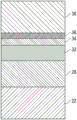
Fig. 1 is a schematic cross-sectional view of an upper portion of a MEMS resonator device including a top-side electrode overlaid with a hermetic layer, an interface layer, a self-assembled monolayer, and a functionalized layer (e.g., a specific binding material), according to one embodiment.
Fig. 2A is a schematic cross-sectional view of a portion of a MEMS resonator device including an active region having a piezoelectric material disposed between overlapping portions of a top side electrode and a bottom side electrode, according to another embodiment.
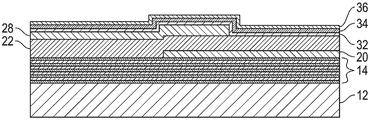
Fig. 2B is a schematic cross-sectional view of the MEMS resonator apparatus of fig. 2A after depositing a hermetic layer over the top-side electrode and the piezoelectric material.
Fig. 2C is a schematic cross-sectional view of the MEMS resonator device of fig. 2B after depositing an interfacial layer over the hermetic layer.
Fig. 2D is a schematic cross-sectional view of the MEMS resonator apparatus of fig. 2C after forming a self-assembled monolayer over the interfacial layer.
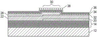
Fig. 2E is a schematic cross-sectional view of the MEMS resonator device of fig. 2D after applying a functionalizing material to a portion of the self-assembled monolayer to overlap an active area of the MEMS resonator device.
Fig. 3A is a schematic cross-sectional view of the MEMS resonator device of fig. 2D after forming walls to define lateral boundaries of a microfluidic channel containing an active area of the MEMS resonator device.
Fig. 3B is a schematic cross-sectional view of the device of fig. 3A after applying a functionalizing material to a portion of the self-assembled monolayer to overlap the active area of the MEMS resonator device.
Fig. 3C is a schematic cross-sectional view of the apparatus of fig. 3B after applying a barrier material on portions of the self-assembled monolayer that are not coincident with the active region.
Fig. 3D is a schematic cross-sectional view of the device of fig. 3C after applying a cover or cap layer over the walls to enclose the microfluidic channel containing the active area of the MEMS resonator device.
Fig. 4 is a top plan view photograph of a bulk acoustic wave MEMS resonator device suitable for receiving a hermetic layer, an interfacial layer, a self-assembled monolayer, and a functionalized (e.g., specific binding) material as disclosed herein.
Figure 5 is a perspective assembly view of a microfluidic device incorporating a substrate with a multiple bulk acoustic wave MEMS resonator device, an intermediate layer defining a channel containing an active area of the MEMS resonator device, and a cover layer.
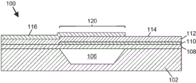
Fig. 6 is a schematic cross-sectional view of a Film Bulk Acoustic Resonator (FBAR) structure that may be used in devices according to certain embodiments, wherein the FBAR structure includes a tilted c-axis hexagonal crystal structure piezoelectric material, a base defining a cavity covered by a support layer, and an active region aligned with the cavity, wherein a portion of the piezoelectric material is disposed between overlapping portions of a top-side electrode and a bottom-side electrode.
Detailed description of the invention
The embodiments set forth below represent the necessary information to enable those skilled in the art to practice the invention and illustrate the best mode of practicing the invention. Upon reading the following description in light of the accompanying drawing figures, those skilled in the art will understand the concepts of the invention and will recognize applications of these concepts not particularly addressed herein. It should be understood that these concepts and applications fall within the scope of the disclosure and the accompanying claims.
It will be understood that, although the terms first, second, etc. may be used herein to describe various elements, these elements should not be limited by these terms. These terms are only used to distinguish one element from another. For example, a first element could be termed a second element, and, similarly, a second element could be termed a first element, without departing from the scope of the present disclosure. As used herein, the term "and/or" includes any and all combinations of one or more of the associated listed terms.
Relative terms, such as "below" or "above" or "upper" or "lower" or "horizontal" or "vertical," may be used herein to describe one element, layer or region's relationship to another element, layer or region as illustrated. It will be understood that these terms and those discussed above are intended to encompass different orientations of the device in addition to the orientation depicted in the figures.
The terminology used herein is for the purpose of describing particular embodiments only and is not intended to be limiting of the disclosure. As used herein, the singular forms "a", "an" and "the" are intended to include the plural forms as well, unless the context clearly indicates otherwise. It will be further understood that the terms "comprises," "comprising," "includes" and/or "including," when used herein, specify the presence of stated features, integers, steps, operations, elements, and/or components, but do not preclude the presence or addition of one or more other features, integers, steps, operations, elements, components, and/or groups thereof. As used herein, the terms "proximate" and "adjacent," when applied to a specified layer or element, refer to a state of being proximate or near another layer or element and encompass the possible presence of one or more intervening layers or elements, without necessarily requiring that the specified layer or element be directly on or directly in contact with the other layer or element, unless the context dictates otherwise.
Unless otherwise defined, all terms (including technical and scientific terms) used herein have the same meaning as commonly understood by one of ordinary skill in the art to which this disclosure belongs. It will be further understood that terms used herein should be interpreted as having a meaning that is consistent with their meaning in the context of this specification and the relevant art and will not be interpreted in an idealized or overly formal sense unless expressly so defined herein.
The present invention relates in one aspect to a micro-electro-mechanical system (MEMS) resonator device comprising a passive structure disposed over a topside electrode of a bulk acoustic wave resonator structure and adapted to receive a functionalized material, such as including but not limited to a specific binding material for biofunctionalization. The passive structure includes (i) a structure having a low water vapor transmission rate (e.g., no greater than 0.1 (g/m)2A/day) a hermetic layer of dielectric material, and (ii) an interfacial layer (e.g., comprising a material having a hydroxylated oxide surface, or comprising gold or another noble metal). In combination, the above-described hermetic and interfacial layers may be considered as a double layer. After deposition of these layers, a SAM may be formed over the interfacial layer, depending on the composition of the interfacial layer, wherein the SAM preferably comprises an organosilane material or a thiol material, the SAM being provided between the interfacial layer and the functionalized material. The gas-tight layer protects the reactive electrode material (e.g., aluminum or aluminum alloy) from the corrosive liquid environment, and the interfacial layer facilitates proper chemical bonding of the SAM.
In certain embodiments, a bulk acoustic wave resonator structure disposed over at least a portion of a substrate includes a piezoelectric material, a top side electrode disposed over a portion of the piezoelectric material, and a bottom side electrode disposed between the piezoelectric material and the substrate, wherein a portion of the piezoelectric material is disposed between the top side electrode and the bottom side electrode to form an active region. In certain implementations, the piezoelectric material comprises a hexagonal crystal structure piezoelectric material (e.g., aluminum nitride or zinc oxide) that includes a c-axis having an orientation distribution that is substantially non-parallel (and may also be non-perpendicular) to a normal to a face of the substrate. A method for forming a hexagonal-crystal-structure piezoelectric material including a c-axis having an orientation distribution that is substantially non-parallel to a normal to a face of a substrate is disclosed in U.S. patent application No. 15/293,063 filed on 10/13/2016, which is hereby incorporated by reference. Other methods for forming piezoelectric materials having an inclined c-axis orientation are disclosed in U.S. patent No. 4,640,756 issued 2/3 1987, the foregoing patents being incorporated herein by reference.
In certain embodiments, the hermetic layer and the interfacial layer can be applied via one or more deposition processes such as Atomic Layer Deposition (ALD), Chemical Vapor Deposition (CVD), or Physical Vapor Deposition (PVD). Of the above processes, ALD is preferred for depositing at least the hermetic layer (and may also be preferred for depositing the interfacial layer) to provide a pinhole free layer structure due to its ability to provide excellent conformal coatings and good step coverage over device features. In addition, ALD is capable of forming a thin, uniform layer that provides relatively little damping of acoustic vibrations that would otherwise result in device performance degradation. The adequacy of coverage is important for the hermetic layer to avoid corrosion of the underlying electrode. If ALD is used to deposit the hermetic layer, in certain embodiments, the hermetic layer may include a thickness in a range from about 5nm to about 100nm, from about 5nm to about 50nm, or from about 10nm to about 25 nm. In certain embodiments, the hermetic layer is about 15nm thick, or about 12nm to about 18nm thick. Conversely, if another process is used, such as CVD, the hermetic layer may include a thickness in the range of about 80nm to about 150nm or more, or in the range of about 80nm to about 120 nm. In view of the above two processes, the thickness of the inner liner may range from about 5nm to about 150 nm. If ALD is used to deposit the interfacial layer, the interfacial layer may include a thickness in a range from about 5nm to about 15 nm. In certain embodiments, the interfacial layer may comprise a thickness in the range of about 10nm or about 8nm to about 12 nm. Other interfacial layer thickness ranges and/or deposition techniques besides ALD may be used in certain embodiments.
In certain embodiments, the hermetic layer and the interfacial layer can be applied sequentially in a vacuum environment, thereby facilitating a high quality interface between the two layers.
In certain embodiments, the hermetic layer includes a material that functions as a dielectric material and has a low water vapor transmission rate (e.g., no greater than 0.1 (g/m)2A/day)) oxide, nitride or oxynitride material. In certain embodiments, the hermetic layer comprises Al2O3Or SiN. In certain embodiments, the interfacial layer comprises SiO2、TiO2Or Ta2O5、HfO2Or Al2O3At least one of (1). In certain embodiments, multiple materials may be combined in a single innerliner, and/or the innerliner may include multiple sub-layers of different materials. Preferably, the hermetic layer is further selected to promote compatibility with the underlying reactive metal (e.g., aluminum or aluminum alloy) electrode structure of the acoustic resonator structure. Although aluminum or an aluminum alloy is often used as an electrode material in the bulk acoustic wave resonator, various transition metals and post-transition metals can be used for such an electrode.
In certain embodiments, the interfacial layer comprises a hydroxylated oxide surface adapted to receive an organosilane based SAM. A preferred interfacial layer material comprising a hydroxylated oxide surface is silicon dioxide SiO2]. Alternative materials for bonding to hydroxylated oxide surfaces include titanium dioxide [ TiO ]2]Tantalum pentoxide [ Ta ]2O5]Hafnium oxide [ HfO ]2]Or alumina [ Al ]2O3]. Other alternatives to incorporate hydroxylated oxide surfaces are known to those skilled in the art and such alternatives are considered to be within the scope of the present disclosure.
In other embodiments, the interfacial layer comprises gold or a noble metal suitable for receiving a thiol-based SAM.
After the interfacial layer is deposited, a SAM is preferably formed thereon. SAMs are typically formed by exposing a solid surface to amphiphilic molecules having chemical groups that exhibit strong affinity for the solid surface. When an interfacial layer comprising a hydroxylated oxide surface is used, then the organosilane SAM layer is particularly preferred for attachment to the hydroxylated oxide surface. The organosilane SAM promotes surface bonding through silicon-oxygen (Si-O) bonds. More specifically, organosilane molecules include hydrolysis-sensitive groups and organic groups, and thus can be used to couple inorganic materials to organic polymers. Organosilane SAMs can be formed by exposing a hydroxylated surface to an organosilane material in the presence of trace amounts of water to form intermediate silanol groups. These groups then react with free hydroxyl groups on the hydroxylated oxide surface to covalently immobilize the organosilane. Examples of possible organosilane based SAMs that are compatible with the interfacial layer that binds the hydroxylated oxide surface include 3-Glycidoxypropyltrimethoxysilane (GPTMS), 3-mercaptopropyltrimethoxysilane (MPTMS), 3-Aminopropyltrimethoxysilane (APTMS), and Octadecyltrimethoxysilane (OTMS), including ethoxy-and chloro-variants thereof. Additional silanes that can be used for the SAM include poly (ethylene glycol) (PEG) conjugated variants. Those skilled in the art will recognize that other alternatives exist and are considered to be within the scope of the present disclosure. Exemplary SAMs may include a thickness in the range of at least 0.5nm or greater.
When using an interfacial layer comprising gold or another noble metal, then a thiol-based (e.g. alkanethiol-based) SAM layer may be used. Alkanethiols are molecules with an alkyl chain as backbone, a tail group and an S-H head group. Thiols can be used for the noble metal interfacial layer due to the strong affinity of sulfur for these metals. Examples of thiol-based SAMs that may be used include, but are not limited to, 1-dodecanethiol (DDT), 11-mercaptoundecanoic acid (MUA), and hydroxyl-terminated (hexaethyleneglycol) undecanethiol (1-UDT). These thiols contain the same backbone but different end groups-i.e., methyl (CH) for DDT, MUA and 1-UDT, respectively3) Carboxyl (COOH) and hydroxyl-terminated hexaethylene glycol (HO- (CH)2CH2O)6). In certain embodiments, the SAM may be formed by incubating the gold surface in a thiol solution using a suitable solvent, such as absolute ethanol.
After the SAM is formed, a functionalized (e.g., specific binding or non-specific binding) material may be applied thereto. In certain embodiments, the functionalizing material may be applied on or over the SAM using microarray spotting pins or other suitable methods. Examples of specific binding materials include, but are not limited to, antibodies, receptors, ligands, and the like. The specific binding material is preferably configured to receive a predetermined target substance (e.g., a molecule, protein, DNA, virus, bacteria, etc.). The functionalized layer comprising the specific binding material may comprise a thickness in the range of about 5nm to 1000nm or about 5nm to about 500 nm. In certain embodiments, an array of different functionalizing materials may be provided over different active regions of a plurality of resonator devices, optionally in combination with one or more active regions that do not contain a functionalizing material to serve as a comparison (or "reference") region. In certain embodiments, the functionalizing material may provide a non-specific binding effect.
Certain embodiments relate to fluidic devices comprising one or more baw MEMS resonator structures as disclosed herein and comprising a fluidic channel (e.g., channel, chamber, etc.) arranged to direct a liquid to contact at least one functionalized (e.g., specifically binding) material arranged on at least one active area of the resonator structure. Such devices may be microfluidic scale and include at least one microfluidic channel (e.g., having at least one dimension, such as a height and/or width of no greater than about 500 microns, or about 250 microns, or about 100 microns). For example, after fabricating a bulk acoustic wave MEMS resonator structure and depositing a gas barrier and an interface layer (optionally followed by deposition of a SAM and at least one functionalizing material) on portions thereof, the microfluidic device may be fabricated by: one or more walls defining lateral boundaries of a microfluidic channel on the first bulk acoustic wave MEMS resonator structure are formed, with an active area thereof disposed along a bottom surface of the microfluidic channel, and then the microfluidic channel is closed using a cover or cap layer that may define a fluidic interface (e.g., an opening) enabling fluid communication with the microfluidic channel. In certain embodiments, the SAM and/or functionalizing (e.g., specific binding) material may be pre-applied to the active region of the bulk acoustic wave MEMS resonator structure prior to forming the microfluidic channel; in other embodiments, the SAM and/or the functionalizing material may be applied on the active region of the bulk acoustic wave resonator structure after the formation of the microfluidic channel.
An example of a MEMS resonator device with multiple stacked lids for providing biosensing utility is provided in fig. 1, according to one embodiment. Fig. 1 is a schematic cross-sectional view of an upper portion of a MEMS resonator device including a piezoelectric material 22 and a top-side electrode 28, wherein at least the top-side electrode 28 is overlaid with a hermetic layer 32, an interface layer 34, a self-assembled monolayer 36, and a functionalized layer (e.g., a specific binding material) 38. In certain embodiments, the MEMS resonator device comprises a bulk acoustic wave resonator device and the piezoelectric material 22 comprises an aluminum nitride or zinc oxide material comprising a c-axis having a distribution of orientations that are substantially non-parallel (and may also be non-perpendicular) to a normal to a face of the substrate. Such orientation distribution enables shear displacement, which advantageously enables the MEMS resonator device to be operated with a liquid, for example in a sensor and/or a microfluidic device. In certain embodiments, the piezoelectric material comprises a c-axis having a longitudinal orientation.
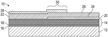
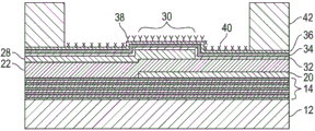
A representative bulk acoustic wave MEMS resonator device 10 suitable for receiving a passive structure, a SAM and at least one functionalizing material (e.g., a specific binding material) is shown in fig. 2A. The device 10 includes a substrate 12 (e.g., typically silicon or another semiconductor material), an acoustic reflector 14 disposed on the substrate 12, a layer of piezoelectric material 22, and bottom and top side electrodes 20, 28. The bottom side electrode 20 is disposed along a portion of the lower surface 24 of the piezoelectric material 22 (between the acoustic reflector 14 and the piezoelectric material 22), and the top side electrode 28 is disposed along a portion of the upper surface 26 of the piezoelectric material 22. The area where the piezoelectric material 22 is disposed between the overlapping portions of the top side electrode 28 and the bottom side electrode 20 is considered to be the active area 30 of the resonator device 10. At least a portion of each of the hermetic layer, the interface layer, and the SAM is disposed on the at least one active area. The acoustic reflector 14 serves to reflect the sound waves and thus reduce or avoid their dissipation in the substrate 12. In certain embodiments, the acoustic reflector 14 comprises a different material (e.g., silicon oxycarbide [ SiOC ]]Silicon nitride [ Si ]3N4]Silicon dioxide [ SiO ]2]Aluminum nitride [ AlN ]]Tungsten [ W ]]And molybdenum [ Mo ]]) Optionally in the form of a quarter-wave bragg mirror, is deposited on the substrate12, respectively. In certain embodiments, other types of acoustic reflectors may be used. The steps for forming the resonator device 10 may include depositing the acoustic reflector 14 on the substrate 12, then depositing the bottom side electrode 20, then growing (e.g., via sputtering or other suitable method) the piezoelectric material 22, then depositing the top side electrode 28.
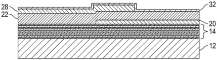
Fig. 2B is a schematic cross-sectional view of MEMS resonator device 10 of fig. 2A after deposition of hermetic layer 32 over top-side electrode 28 and portions of piezoelectric material 22. The air barrier 32 preferably includes a material having a low water vapor transmission rate (e.g., no greater than 0.1 (g/m)2Day) of the dielectric material. In certain embodiments, the hermetic layer 32 comprises an oxide, nitride, or oxynitride material, such as (but not limited to) Al2O3Or SiO2One or more of (a).
Fig. 2C is a schematic cross-sectional view of the coated MEMS resonator device of fig. 2B after depositing an interface layer 34 over the hermetic layer 32. Interfacial layer 34 comprises a hydroxylated oxide surface and may comprise silicon dioxide SiO in certain embodiments2]Titanium dioxide [ TiO ]2]Tantalum pentoxide [ Ta ]2O5]Hafnium oxide [ HfO ]2]Or alumina [ Al ]2O3]One or more of (a).
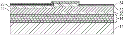
Fig. 2D is a schematic cross-sectional view of the coated MEMS resonator device of fig. 2C after forming a self-assembled monolayer (SAM)36 on the interfacial layer 34. In certain embodiments, the SAM comprises an organosilane material. Examples of suitable SAM materials include GPTMS, MPTMS, APTMS, OTMS, and PEG organosilanes. Other examples of organosilane SAM materials and methods of forming the same are well known to those skilled in the art. In other embodiments, the SAM comprises a thiol material.
Fig. 2E is a schematic cross-sectional view of the MEMS resonator device of fig. 2D after applying a functionalizing material 38 to a portion of the self-assembled monolayer 36 to overlap the active area 30 of the resonator device. As shown, the functionalizing material 38 overlaps the active region 30 of the device. The device of fig. 2E can be used as a sensor to detect the presence of a target substance in an environment. When an acoustic wave is induced in the active region 30 and the functionalized material 38 is exposed to a target substance bound to the functionalized material 38, a change in one or more wave propagation properties (e.g., frequency, amplitude, and/or phase characteristics) of the device may be detected to indicate the presence and/or amount of the target substance in the environment.
In certain embodiments, a barrier layer can be disposed (e.g., patterned) over a SAM region where no functionalized (e.g., specific binding) material is present or desired, wherein the barrier layer can be used to prevent non-specific binding of non-target species to the SAM. Examples of barrier materials that can be used include non-oxide films such as silicon nitride [ SiN ] or silicon carbide [ SiC ]; organic materials such as SU8, photoresist, polyimide, parylene or poly (ethylene glycol) [ PEG ]; or a chemical or biological buffer or protein (e.g., Bovine Serum Albumin (BSA)).
Certain embodiments relate to a microfluidic device comprising a MEMS resonator device as disclosed herein and comprising a fluid channel arranged to direct a liquid to contact at least one functionalizing material. For example, after fabrication of the MEMS resonator device and application of the passive structures (e.g., the gas barrier and interface layer) and SAM thereon, the fluidic device may be fabricated by forming one or more walls defining the lateral boundaries of the microfluidic channel, preferably containing the active area of at least one acoustic resonator, followed by application of a cover or capping layer to close the microfluidic channel. In certain embodiments, the functionalizing (e.g., specific binding) material may be applied after the walls of the microfluidic channel are formed but before the cover or cap layer is applied.
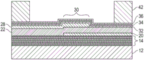
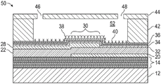
Figures 3A-3D illustrate the formation of a fluidic device including a bulk acoustic wave MEMS resonator device. Fig. 3A is a schematic cross-sectional view of the MEMS resonator device of fig. 2D after forming walls 42 to define lateral boundaries of a microfluidic channel containing an active area of the MEMS resonator device. The MEMS resonator device comprises a substrate 12, an acoustic reflector 14 arranged above the substrate 12, a layer of piezoelectric material 22, and a bottom side electrode 20 and a top side electrode 28 arranged below and above an area of the piezoelectric material 22, respectively. The region of the piezoelectric material 22 disposed between the overlapping portions of the top side electrode 28 and the bottom side electrode 20 defines an active region 30. A gas barrier 32 is provided over the top side electrode 28 and the piezoelectric material 22, an interface layer 34 is disposed over the gas barrier 32, and a SAM 36 is provided over the interface layer 34. A wall 42 laterally offset from active region 30 extends upwardly from SAM 36 to define the lateral boundaries of the microfluidic channel comprising active region 30. Such walls may be formed of any suitable material, such as a laser cut "stencil" layer of SU-8 negative epoxy resist, other photoresist material, or a thin polymer material, optionally including one or more self-adhesive surfaces (e.g., tape). Optionally, such walls 42 may be formed prior to deposition of the SAM and the functionalization and barrier layers with SU-8 negative epoxy resist or other photoresist material.
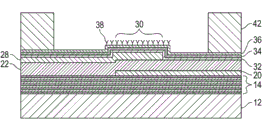
Fig. 3B is a schematic cross-sectional view of the device of fig. 3A after applying a functionalizing (e.g., specific binding) material 38 to a portion of the SAM 36 to overlap the active region 30 of the resonator device. In certain embodiments, the functionalizing material 38 may be applied on or over the SAM 36 using a microarray pin or other suitable method, wherein the functionalizing material 38 preferably overlaps the active region 30.
Fig. 3C is a schematic cross-sectional view of the apparatus of fig. 3B after applying a barrier material 40 over portions of the SAM 36 that are not coincident with the active region 30. Examples of suitable barrier materials may include Bovine Serum Albumin (BSA).
Fig. 3D is a schematic cross-sectional view of the device of fig. 3C after applying a cover or capping layer 44 on the wall 42 to create a microfluidic device 50, the microfluidic device 50 including an enclosed microfluidic channel 52, the enclosed microfluidic channel 52 containing the active region 30 overlaid with the functionalizing material 38. The cover or cap layer 44 includes ports 46, 48 that can be used to supply fluids (e.g., liquids) into the microfluidic channel 52. The cover or cap layer 44 may be present as any suitable material that is compatible with the fluid, and in certain embodiments the cover or cap layer 44 may be optically transmissive. Examples of desirable materials for the cover or cap layer 44 include, but are not limited to, polymeric materials such as polypropylene, polyethylene, polycarbonate, and the like or inorganic non-metallic materials such as ceramics or glass. In use of the microfluidic device 50, liquid may be supplied through one of the ports 46, 48 into the microfluidic channel 52 to contact the functionalizing material 38. When an acoustic wave is induced in the active region 30 and a target substance contained in the liquid supplied to the microfluidic channel 52 binds with the functionalizing material 38, a change in one or more wave propagation properties (e.g., frequency, amplitude, and/or phase characteristics) of the MEMS resonator device may be detected to indicate the presence and/or amount of the target substance in the liquid. The presence of the gas barrier 32 prevents the liquid from corroding the top-side electrode 28, while the interface layer 34 facilitates the connection of the SAM 36, enabling the application of the functionalizing material 38.
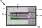
Fig. 4 is a top plan view of a bulk acoustic wave MEMS resonator device 10 (consistent with device 10 shown in fig. 2A) adapted to receive a hermetic layer, an interfacial layer, a self-assembled monolayer, and a functionalized (e.g., specifically bonded) material as disclosed herein. The MEMS resonator device 10 includes a piezoelectric material (not shown) disposed over a substrate 12, a bottom side electrode 20 disposed under a portion of the piezoelectric material, and a top side electrode 28 disposed over a portion of the piezoelectric material, including an active region 30, wherein the piezoelectric material is disposed between overlapping portions of the top side electrode 28 and the bottom side electrode 20. Externally accessible contacts 20A, 28A are in electrical communication with the bottom side electrode 20 and the top side electrode 28, respectively. After the MEMS resonator device 10 is overlaid with the interface layers, self-assembled monolayers, and functionalized (e.g., specific binding) materials disclosed herein, the device 10 can be used as a sensor and/or bound to a microfluidic device. If desired, a plurality of MEMS resonator devices 10 may be provided in an array on a single substrate 12.
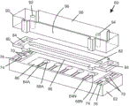
Fig. 5 is a perspective assembly view of a microfluidic device 60 incorporating a substrate 62 having a plurality of bulk acoustic wave MEMS resonator devices, an intermediate layer 80 defining a central microfluidic channel 82 aligned with the active areas 68A-68N of the MEMS resonator devices, and a cover or cap layer 90 disposed to cover the intermediate layer 80. The top central portion of the substrate 62, which includes an acoustic reflector (not shown) and piezoelectric material (not shown), includes a top side electrode 66 and bottom side electrodes 64A-64N. The regions where the electrodes overlap each other and include piezoelectric material are represented as active regions 68A-68N. Any suitable number of active regions 68A-68N may be provided and fluidly arranged in series or parallel, although five are shown in fig. 5. The top peripheral (or top) portion of substrate 62 further includes a reference top side electrode 76 and a reference bottom side electrode 74 in communication with reference overlap region 70. Such reference overlap regions 70 are not exposed to fluid and are present to provide a basis for comparing signals obtained from the active regions 68A-68N exposed to fluid within the central microfluidic channel 82. The substrate 62 is overlaid with an intermediate layer 80, wherein a central microfluidic channel 82 is intended to receive a fluid and defines a peripheral chamber 84, which peripheral chamber 84 is arranged to cover the reference overlap region 70 in a sealing manner. The intermediate layer 80 may be formed of any suitable material, such as a SU-8 negative epoxy resist, other photoresist material, or a laser cut "stencil" layer of thin polymer material, optionally including one or more self-adhesive surfaces (e.g., tape), or the like. The intermediate layer 80 further includes lateral insertion regions 86, the lateral insertion regions 86 enabling access to lateral portions of the top side electrodes 66 and the bottom side electrodes 64A-64N after assembly of the microfluidic device 60. The cover or overlay 90 includes a lateral insertion region 96 aligned with the lateral insertion region 86 of the intermediate layer 80, and includes microfluidic ports 92, 94 accessible along a top surface 98 and aligned with ends of the central microfluidic channel 82 defined in the intermediate layer 80 to allow fluid (e.g., liquid) to be supplied to the central microfluidic channel 82 over the active regions 68A-68N. Preferably, at least the electrodes 64A-64N, 66 are overlaid with the hermetic layers, interfacial layers, self-assembled monolayers, and functionalized (e.g., specific binding) materials disclosed herein. As will be appreciated by those skilled in the art upon review of the present disclosure, microfluidic devices according to other configurations may be provided.
Fig. 6 is a schematic cross-sectional view of a Film Bulk Acoustic Resonator (FBAR) structure 100 including an active region, wherein at least a portion of FBAR structure 100 is subject to overlap with an interface layer and a self-assembled monolayer (SAM) adapted to receive a functionalized material (e.g., a specific binding or non-specific binding material), according to an embodiment. FBAR structure 100 includes a substrate 102 (e.g., silicon or another semiconductor material) that defines a cavity 106 covered by a handle layer 108 (e.g., silicon dioxide). Bottom side electrode 110 is disposed over a portion of support layer 108, a layer of piezoelectric material 112, preferably exhibiting a tilted c-axis hexagonal crystal structure piezoelectric material (e.g., AlN or ZnO), is disposed over bottom side electrode 110 and support layer 108, and a top side electrode 116 is disposed over at least a portion of a top surface 114 of piezoelectric material layer 112. A portion of the piezoelectric material layer 112 disposed between the top side electrode 116 and the bottom side electrode 110 is present as an active region 120 of the FBAR structure 100. Active region 120 is disposed over and aligned with cavity 106, and cavity 106 is disposed under handle layer 108. The cavity 106 serves to confine acoustic waves induced in the active region 120 by preventing acoustic energy from dissipating into the substrate 102, since the acoustic waves do not propagate efficiently through the cavity 106. In this regard, the cavity 106 provides an alternative to the acoustic reflector 14 shown in fig. 2A-3D. Although the cavity 106 shown in fig. 6 is defined by a thinned portion of the substrate 102 from below, in alternative embodiments, at least a portion of the cavity 106 may extend through the entire thickness of the substrate 102. The steps for forming FBAR structure 100 may include defining a cavity 106 in substrate 102, filling cavity 106 with a sacrificial material (not shown), optionally followed by planarization of the sacrificial material, depositing handle layer 108 over substrate 102 and the sacrificial material, removing the sacrificial material (e.g., by flowing an etchant through vertical openings defined in either substrate 102 or handle layer 108 or lateral edges of substrate 102), depositing bottom side electrode 110 over handle layer 108, growing (e.g., via sputtering or other suitable methods) piezoelectric material layer 112, and depositing top side electrode 116.
As will be recognized by those skilled in the art upon review of the present disclosure, in certain embodiments, the FBAR structure of fig. 6 may be replaced with a fixedly mounted BAW structure as disclosed in fig. 2A-3D, wherein at least a portion of the bulk acoustic wave structure is overlaid with an interface layer and a self-assembled monolayer suitable for receiving a functionalized material (e.g., a specific binding or non-specific binding material).
Those skilled in the art will recognize improvements and modifications to the preferred embodiments of the present disclosure. All such improvements and modifications are considered within the scope of the concepts disclosed herein and the claims that follow.
Claims (20)
1. A microelectromechanical systems resonator device, comprising:
a substrate;
a bulk acoustic wave resonator structure disposed over at least a portion of the substrate, the bulk acoustic wave resonator structure comprising at least one top side electrode;
an air barrier disposed over at least a portion of the at least one top-side electrode, the air barrier comprising a dielectric material comprising no greater than 0.1g/m2Water vapor transmission rate per day;
an interface layer disposed over at least a portion of the air barrier; and
at least one functionalizing material disposed over at least a portion of the interfacial layer;
wherein the bulk acoustic wave resonator structure includes at least one active area below the at least one top side electrode, and at least a portion of each of the gas barrier, the interfacial layer, and the at least one functionalization material is disposed over the at least one active area.
2. The mems resonator device of claim 1, further comprising a self-assembled monolayer disposed between the interface layer and the at least one functionalizing material.
3. The microelectromechanical systems resonator apparatus of claim 2, wherein the interfacial layer comprises a hydroxylated oxide surface and the self-assembled monolayer comprises an organosilane material.
4. The mems resonator apparatus of claim 2, wherein the interface layer comprises gold or another noble metal, and the self-assembled monolayer comprises a thiol material.
5. The mems resonator device of claim 1, wherein the hermetic layer comprises an oxide, nitride, or oxynitride material.
6. The microelectronic machine of claim 1Mechanical system resonator device, wherein said interfacial layer comprises SiO2,TiO2,Ta2O5,HfO2Or Al2O3At least one of (1).
7. The mems resonator device of claim 1, wherein the at least one top side electrode comprises a non-noble metal.
8. The mems resonator device of claim 1, wherein the hermetic layer comprises a thickness in a range from about 5nm to about 150nm and the interfacial layer comprises a thickness in a range from about 5nm to about 15 nm.
9. The mems resonator device of claim 1, wherein the bulk acoustic wave resonator structure comprises a hexagonal-crystal structure piezoelectric material comprising a c-axis having a distribution of orientations that are substantially non-parallel to a normal to a face of the substrate.
10. The mems resonator device of claim 1, further comprising an acoustic reflector structure disposed between the substrate and the bulk acoustic wave resonator structure, wherein the bulk acoustic wave resonator structure comprises a fixedly mounted bulk acoustic wave resonator structure.
11. The mems resonator device of claim 1, wherein the substrate defines a recess, a support layer is provided between the bulk acoustic wave resonator structure and the recess, and the at least one active region is disposed over at least a portion of the support layer and at least a portion of the recess.
12. A sensor comprising the mems resonator device of claim 1.
13. A fluidic device comprising the microelectromechanical system resonator device of claim 1 and a fluidic channel arranged to direct a liquid to contact the at least one functionalization material.
14. A method for biological or chemical sensing, the method comprising:
supplying a fluid comprising a target substance into a fluid channel of a fluidic device according to claim 13, wherein the supplying is configured to bind at least some of the target substance to at least one functionalized material;
inducing bulk acoustic waves in the at least one active region; and
sensing a change in at least one of a frequency property, an amplitude property, or a phase property of the bulk acoustic wave resonator structure to indicate at least one of a presence or an amount of a target substance bound to the at least one functionalizing material.
15. A method for fabricating a microelectromechanical systems resonator device, the method comprising:
forming at least one top-side electrode over at least a portion of a piezoelectric material disposed over at least a portion of a substrate;
depositing a hermetic layer over at least a portion of the at least one top-side electrode, the hermetic layer comprising a dielectric material comprising no more than 0.1g/m2Water vapor transmission rate per day;
depositing an interfacial layer over at least a portion of the hermetic layer; and
depositing at least one functionalizing material on at least a portion of the interfacial layer;
wherein the resonator device includes at least one active area below the at least one top-side electrode, and at least a portion of each of the hermetic layer, the interface layer, and the at least one functionalizing material is disposed above the at least one active area.
16. The method of claim 15, wherein the depositing of the hermetic layer comprises atomic layer deposition and the depositing of the interfacial layer comprises at least one of chemical vapor deposition, atomic layer deposition, or physical vapor deposition.
17. The method of claim 15, wherein the depositing of the interfacial layers is performed sequentially in a vacuum environment after the depositing of the hermetic layer.
18. The method of claim 15, further comprising forming a self-assembled monolayer on at least a portion of the interfacial layer prior to depositing the at least one functionalizing material.
19. The method of claim 18, further comprising depositing a barrier material over a portion of the self-assembled monolayer that is not coincident with the at least one functionalizing material.
20. The method of claim 15, further comprising forming at least one wall over a portion of the interface layer and defining a fluid channel.
Applications Claiming Priority (3)
| Application Number | Priority Date | Filing Date | Title |
|---|---|---|---|
| US201562252402P | 2015-11-06 | 2015-11-06 | |
| US62/252402 | 2015-11-06 | ||
| PCT/US2016/058745 WO2017078992A1 (en) | 2015-11-06 | 2016-10-26 | Acoustic resonator devices and fabrication methods providing hermeticity and surface functionalization |
Publications (2)
| Publication Number | Publication Date |
|---|---|
| CN108474764A CN108474764A (en) | 2018-08-31 |
| CN108474764B true CN108474764B (en) | 2021-12-10 |
Family
ID=57256432
Family Applications (1)
| Application Number | Title | Priority Date | Filing Date |
|---|---|---|---|
| CN201680078230.7A Active CN108474764B (en) | 2015-11-06 | 2016-10-26 | Acoustic resonator device and manufacturing method providing gas tightness and surface functionalization |
Country Status (5)
| Country | Link |
|---|---|
| US (1) | US10302595B2 (en) |
| EP (1) | EP3371583A1 (en) |
| JP (1) | JP6882280B2 (en) |
| CN (1) | CN108474764B (en) |
| WO (1) | WO2017078992A1 (en) |
Families Citing this family (8)
| Publication number | Priority date | Publication date | Assignee | Title |
|---|---|---|---|---|
| US10352904B2 (en) | 2015-10-26 | 2019-07-16 | Qorvo Us, Inc. | Acoustic resonator devices and methods providing patterned functionalization areas |
| US10371667B2 (en) * | 2015-11-16 | 2019-08-06 | Qorvo Us, Inc. | BAW sensor with passive mixing structures |
| US10267770B2 (en) | 2016-07-27 | 2019-04-23 | Qorvo Us, Inc. | Acoustic resonator devices and methods with noble metal layer for functionalization |
| WO2018031055A1 (en) | 2016-08-11 | 2018-02-15 | Qorvo Us, Inc. | Acoustic resonator device with controlled placement of functionalization material |
| WO2021021739A1 (en) | 2019-07-31 | 2021-02-04 | QXONIX Inc. | Mass loaded bulk acoustic wave (baw) resonator structures, devices and systems |
| JP7378723B2 (en) * | 2019-09-30 | 2023-11-14 | 国立大学法人東北大学 | elastic wave device |
| CN111351848B (en) * | 2020-03-19 | 2020-10-16 | 山东科技大学 | Preparation method of sensor, sensor and detection method of sensor |
| CN114900147B (en) * | 2022-07-08 | 2022-11-01 | 深圳新声半导体有限公司 | Bulk acoustic wave resonator and method for manufacturing the same |
Citations (18)
| Publication number | Priority date | Publication date | Assignee | Title |
|---|---|---|---|---|
| SU490006A1 (en) * | 1974-05-15 | 1975-10-30 | Ленинградский электротехнический институт | Ultrasonic transducer |
| CN85105865A (en) * | 1985-05-23 | 1986-11-19 | 住友电木株式会社 | gas concentration measurement instrument |
| JPH0946793A (en) * | 1995-07-31 | 1997-02-14 | Taiyo Yuden Co Ltd | Piezoelectric element and piezoelectric audio equipment |
| JP2001251159A (en) * | 2000-03-08 | 2001-09-14 | Mitsubishi Electric Corp | Thin film piezoelectric element and its manufacturing method |
| JP2003037469A (en) * | 2001-07-26 | 2003-02-07 | Matsushita Electric Ind Co Ltd | Piezoelectric thin-film oscillator and frequency adjusting method therefor |
| CN1419895A (en) * | 2001-11-16 | 2003-05-28 | 精工电子有限公司 | Piezoelectric sensor, method for mfg. same, and pulse wave detector |
| KR20060007397A (en) * | 2003-04-26 | 2006-01-24 | 카네쇼 쏘일 트리트먼트 비브이비에이 | Method and device for detecting volatile analytes in air samples |
| CN1864063A (en) * | 2003-10-08 | 2006-11-15 | 皇家飞利浦电子股份有限公司 | Bulk acoustic wave sensor |
| CN101246162A (en) * | 2008-03-12 | 2008-08-20 | 浙江大学 | Immune body detecting biochip using piezo-electricity thin film acoustic wave device |
| JP2008236460A (en) * | 2007-03-22 | 2008-10-02 | Seiko Epson Corp | Piezoelectric oscillator, sensor and multisensor |
| JP2009207075A (en) * | 2008-02-29 | 2009-09-10 | Tdk Corp | Method of manufacturing resonator filter |
| US7656070B2 (en) * | 2005-04-06 | 2010-02-02 | Murata Manufacturing Co., Ltd. | Surface wave sensor apparatus |
| CN102608172A (en) * | 2012-03-12 | 2012-07-25 | 山东科技大学 | Film bulk acoustic galloping resonance biochemistry sensor with direct-current electrodes |
| CN102778509A (en) * | 2012-08-17 | 2012-11-14 | 天津理工大学 | SAW (surface acoustic wave) gas sensor substrate |
| CN103454345A (en) * | 2013-08-20 | 2013-12-18 | 西安交通大学 | Marine biochemical substance monitoring sensor based on CMUT (Capacitive Micromachined Ultrasonic Transducer) as well as manufacturing method and measuring method of marine biochemical substance monitoring sensor |
| CN104034798A (en) * | 2013-03-07 | 2014-09-10 | 浙江工商大学 | Cell suspension concentration detection system and its detection method |
| CN104330470A (en) * | 2014-09-30 | 2015-02-04 | 成都柏森松传感技术有限公司 | SAW sensor-based detection apparatus |
| CN105157935A (en) * | 2015-08-09 | 2015-12-16 | 安徽普为智能科技有限责任公司 | Method for detecting airtight uniformity of lithium battery |
Family Cites Families (21)
| Publication number | Priority date | Publication date | Assignee | Title |
|---|---|---|---|---|
| US4640756A (en) | 1983-10-25 | 1987-02-03 | The United States Of America As Represented By The United States Department Of Energy | Method of making a piezoelectric shear wave resonator |
| US6320295B1 (en) * | 1998-11-18 | 2001-11-20 | Mcgill Robert Andrew | Diamond or diamond like carbon coated chemical sensors and a method of making same |
| US7989851B2 (en) * | 2002-06-06 | 2011-08-02 | Rutgers, The State University Of New Jersey | Multifunctional biosensor based on ZnO nanostructures |
| US7468608B2 (en) | 2002-07-19 | 2008-12-23 | Siemens Aktiengesellschaft | Device and method for detecting a substance of a liquid |
| US20050148065A1 (en) * | 2003-12-30 | 2005-07-07 | Intel Corporation | Biosensor utilizing a resonator having a functionalized surface |
| US7134319B2 (en) * | 2004-08-12 | 2006-11-14 | Honeywell International Inc. | Acoustic wave sensor with reduced condensation and recovery time |
| WO2006063437A1 (en) * | 2004-12-15 | 2006-06-22 | University Of Guelph | Prion sensors for diagnosis of transmissible spongiform encephalopathy or for detection of prions, and use thereof |
| FI118829B (en) * | 2005-07-08 | 2008-03-31 | Valtion Teknillinen | Micromechanical sensor, sensor array and method, and new use of longitudinal acoustic waves |
| CN101180532A (en) * | 2006-04-20 | 2008-05-14 | 多弗电子股份有限公司 | Coating for hostile environment and sensor using the coating |
| US8448494B2 (en) | 2008-12-30 | 2013-05-28 | Stmicroelectronics S.R.L. | Integrated electronic microbalance plus chemical sensor |
| FI20096201A0 (en) * | 2009-11-19 | 2009-11-19 | Valtion Teknillinen | Mass wave resonator and method for its manufacture |
| US20110121916A1 (en) * | 2009-11-24 | 2011-05-26 | Avago Technologies Wireless Ip (Singapore) Pte. Ltd. | Hybrid bulk acoustic wave resonator |
| ES2804799T3 (en) | 2010-10-20 | 2021-02-09 | Qorvo Us Inc | Apparatus and method for measuring binding and concentration kinetics with a resonator sensor |
| JP5075296B2 (en) * | 2011-02-21 | 2012-11-21 | パナソニック株式会社 | MEMS resonator |
| US8896395B2 (en) * | 2011-09-14 | 2014-11-25 | Avago Technologies General Ip (Singapore) Pte. Ltd. | Accoustic resonator having multiple lateral features |
| JP6284076B2 (en) * | 2013-11-22 | 2018-02-28 | 国立大学法人豊橋技術科学大学 | Physical / chemical sensors and methods for measuring specific substances |
| US9910015B2 (en) * | 2014-04-14 | 2018-03-06 | Texas Instruments Incorporated | Sensor array chip with piezoelectric transducer including inkjet forming method |
| US9922809B2 (en) | 2015-10-14 | 2018-03-20 | Qorvo Us, Inc. | Deposition system for growth of inclined c-axis piezoelectric material structures |
| US10352904B2 (en) | 2015-10-26 | 2019-07-16 | Qorvo Us, Inc. | Acoustic resonator devices and methods providing patterned functionalization areas |
| US10267770B2 (en) | 2016-07-27 | 2019-04-23 | Qorvo Us, Inc. | Acoustic resonator devices and methods with noble metal layer for functionalization |
| WO2018031055A1 (en) | 2016-08-11 | 2018-02-15 | Qorvo Us, Inc. | Acoustic resonator device with controlled placement of functionalization material |
-
2016
- 2016-10-26 US US15/334,528 patent/US10302595B2/en active Active
- 2016-10-26 EP EP16794124.4A patent/EP3371583A1/en active Pending
- 2016-10-26 CN CN201680078230.7A patent/CN108474764B/en active Active
- 2016-10-26 JP JP2018522723A patent/JP6882280B2/en active Active
- 2016-10-26 WO PCT/US2016/058745 patent/WO2017078992A1/en active Application Filing
Patent Citations (18)
| Publication number | Priority date | Publication date | Assignee | Title |
|---|---|---|---|---|
| SU490006A1 (en) * | 1974-05-15 | 1975-10-30 | Ленинградский электротехнический институт | Ultrasonic transducer |
| CN85105865A (en) * | 1985-05-23 | 1986-11-19 | 住友电木株式会社 | gas concentration measurement instrument |
| JPH0946793A (en) * | 1995-07-31 | 1997-02-14 | Taiyo Yuden Co Ltd | Piezoelectric element and piezoelectric audio equipment |
| JP2001251159A (en) * | 2000-03-08 | 2001-09-14 | Mitsubishi Electric Corp | Thin film piezoelectric element and its manufacturing method |
| JP2003037469A (en) * | 2001-07-26 | 2003-02-07 | Matsushita Electric Ind Co Ltd | Piezoelectric thin-film oscillator and frequency adjusting method therefor |
| CN1419895A (en) * | 2001-11-16 | 2003-05-28 | 精工电子有限公司 | Piezoelectric sensor, method for mfg. same, and pulse wave detector |
| KR20060007397A (en) * | 2003-04-26 | 2006-01-24 | 카네쇼 쏘일 트리트먼트 비브이비에이 | Method and device for detecting volatile analytes in air samples |
| CN1864063A (en) * | 2003-10-08 | 2006-11-15 | 皇家飞利浦电子股份有限公司 | Bulk acoustic wave sensor |
| US7656070B2 (en) * | 2005-04-06 | 2010-02-02 | Murata Manufacturing Co., Ltd. | Surface wave sensor apparatus |
| JP2008236460A (en) * | 2007-03-22 | 2008-10-02 | Seiko Epson Corp | Piezoelectric oscillator, sensor and multisensor |
| JP2009207075A (en) * | 2008-02-29 | 2009-09-10 | Tdk Corp | Method of manufacturing resonator filter |
| CN101246162A (en) * | 2008-03-12 | 2008-08-20 | 浙江大学 | Immune body detecting biochip using piezo-electricity thin film acoustic wave device |
| CN102608172A (en) * | 2012-03-12 | 2012-07-25 | 山东科技大学 | Film bulk acoustic galloping resonance biochemistry sensor with direct-current electrodes |
| CN102778509A (en) * | 2012-08-17 | 2012-11-14 | 天津理工大学 | SAW (surface acoustic wave) gas sensor substrate |
| CN104034798A (en) * | 2013-03-07 | 2014-09-10 | 浙江工商大学 | Cell suspension concentration detection system and its detection method |
| CN103454345A (en) * | 2013-08-20 | 2013-12-18 | 西安交通大学 | Marine biochemical substance monitoring sensor based on CMUT (Capacitive Micromachined Ultrasonic Transducer) as well as manufacturing method and measuring method of marine biochemical substance monitoring sensor |
| CN104330470A (en) * | 2014-09-30 | 2015-02-04 | 成都柏森松传感技术有限公司 | SAW sensor-based detection apparatus |
| CN105157935A (en) * | 2015-08-09 | 2015-12-16 | 安徽普为智能科技有限责任公司 | Method for detecting airtight uniformity of lithium battery |
Non-Patent Citations (2)
| Title |
|---|
| SAW and BAW technologies for RF filter applications: A review of the relative strengths and weaknesses;Robert Aigner 等;《2008 IEEE Ultrasonics Symposium》;20081105;第582-589页 * |
| 小型化光声光谱气体传感器研究进展;姜萌 等;《激光与光电子学进展》;20150113;第52卷(第2期);第020006-1至020006-11页 * |
Also Published As
| Publication number | Publication date |
|---|---|
| JP6882280B2 (en) | 2021-06-02 |
| WO2017078992A1 (en) | 2017-05-11 |
| EP3371583A1 (en) | 2018-09-12 |
| CN108474764A (en) | 2018-08-31 |
| JP2018533310A (en) | 2018-11-08 |
| US10302595B2 (en) | 2019-05-28 |
| US20170134001A1 (en) | 2017-05-11 |
Similar Documents
| Publication | Publication Date | Title |
|---|---|---|
| CN108474764B (en) | Acoustic resonator device and manufacturing method providing gas tightness and surface functionalization | |
| US11695384B2 (en) | Acoustic resonator device with controlled placement of functionalization material | |
| US10618045B2 (en) | Sensor device with BAW resonator and through-substrate fluidic vias | |
| US10352904B2 (en) | Acoustic resonator devices and methods providing patterned functionalization areas | |
| CN108463720B (en) | Resonator structure with enhanced reflection of shear and longitudinal modes of acoustic vibration | |
| CN109073601B (en) | BAW sensor fluidic device with increased dynamic measurement range | |
| US10326425B2 (en) | Acoustic resonator with reduced mechanical clamping of an active region for enhanced shear mode response | |
| US10371667B2 (en) | BAW sensor with passive mixing structures | |
| US10458982B2 (en) | Fluidic device including BAW resonators along opposing channel surfaces | |
| US10812045B2 (en) | BAW sensor with enhanced surface area active region | |
| US11940415B2 (en) | Fluidic device with fluid port orthogonal to functionalized active region | |
| US11353428B2 (en) | BAW sensor device with peel-resistant wall structure |
Legal Events
| Date | Code | Title | Description |
|---|---|---|---|
| PB01 | Publication | ||
| PB01 | Publication | ||
| SE01 | Entry into force of request for substantive examination | ||
| SE01 | Entry into force of request for substantive examination | ||
| REG | Reference to a national code |
Ref country code: HK Ref legal event code: DE Ref document number: 1260247 Country of ref document: HK |
|
| GR01 | Patent grant | ||
| GR01 | Patent grant |