CN107851081B - Low speed bus time stamping method and circuit - Google Patents
Low speed bus time stamping method and circuit Download PDFInfo
- Publication number
- CN107851081B CN107851081B CN201680043146.1A CN201680043146A CN107851081B CN 107851081 B CN107851081 B CN 107851081B CN 201680043146 A CN201680043146 A CN 201680043146A CN 107851081 B CN107851081 B CN 107851081B
- Authority
- CN
- China
- Prior art keywords
- clock signal
- slave device
- time
- communication link
- master device
- Prior art date
- Legal status (The legal status is an assumption and is not a legal conclusion. Google has not performed a legal analysis and makes no representation as to the accuracy of the status listed.)
- Active
Links
- 238000000034 method Methods 0.000 title claims abstract description 36
- 230000007704 transition Effects 0.000 claims abstract description 146
- 238000004891 communication Methods 0.000 claims abstract description 87
- 230000004044 response Effects 0.000 claims abstract description 27
- 230000008859 change Effects 0.000 claims description 34
- 238000012806 monitoring device Methods 0.000 claims description 24
- 238000001514 detection method Methods 0.000 claims description 22
- 230000001360 synchronised effect Effects 0.000 claims description 16
- 238000004364 calculation method Methods 0.000 claims description 11
- 230000008878 coupling Effects 0.000 claims description 5
- 238000010168 coupling process Methods 0.000 claims description 5
- 238000005859 coupling reaction Methods 0.000 claims description 5
- 238000010586 diagram Methods 0.000 description 27
- 239000003550 marker Substances 0.000 description 27
- 238000005259 measurement Methods 0.000 description 15
- 230000003111 delayed effect Effects 0.000 description 13
- 230000002093 peripheral effect Effects 0.000 description 9
- 238000004590 computer program Methods 0.000 description 6
- 230000000977 initiatory effect Effects 0.000 description 6
- 230000000630 rising effect Effects 0.000 description 5
- 230000000737 periodic effect Effects 0.000 description 4
- 230000002596 correlated effect Effects 0.000 description 3
- 230000000875 corresponding effect Effects 0.000 description 3
- 230000008569 process Effects 0.000 description 3
- 238000012545 processing Methods 0.000 description 3
- 101100328518 Caenorhabditis elegans cnt-1 gene Proteins 0.000 description 2
- 238000013459 approach Methods 0.000 description 2
- 230000001276 controlling effect Effects 0.000 description 2
- 238000012544 monitoring process Methods 0.000 description 2
- 238000003325 tomography Methods 0.000 description 2
- 230000001960 triggered effect Effects 0.000 description 2
- -1 ... Proteins 0.000 description 1
- 101100328519 Caenorhabditis elegans cnt-2 gene Proteins 0.000 description 1
- XUIMIQQOPSSXEZ-UHFFFAOYSA-N Silicon Chemical compound [Si] XUIMIQQOPSSXEZ-UHFFFAOYSA-N 0.000 description 1
- 210000001015 abdomen Anatomy 0.000 description 1
- 230000009471 action Effects 0.000 description 1
- 230000004913 activation Effects 0.000 description 1
- 230000001413 cellular effect Effects 0.000 description 1
- 230000001934 delay Effects 0.000 description 1
- 230000007613 environmental effect Effects 0.000 description 1
- 239000002184 metal Substances 0.000 description 1
- 229910052751 metal Inorganic materials 0.000 description 1
- 238000012986 modification Methods 0.000 description 1
- 230000004048 modification Effects 0.000 description 1
- 229910052710 silicon Inorganic materials 0.000 description 1
- 239000010703 silicon Substances 0.000 description 1
- 239000000126 substance Substances 0.000 description 1
- 210000001835 viscera Anatomy 0.000 description 1
Images


Classifications
-
- G—PHYSICS
- G06—COMPUTING; CALCULATING OR COUNTING
- G06F—ELECTRIC DIGITAL DATA PROCESSING
- G06F1/00—Details not covered by groups G06F3/00 - G06F13/00 and G06F21/00
- G06F1/04—Generating or distributing clock signals or signals derived directly therefrom
- G06F1/12—Synchronisation of different clock signals provided by a plurality of clock generators
-
- G—PHYSICS
- G06—COMPUTING; CALCULATING OR COUNTING
- G06F—ELECTRIC DIGITAL DATA PROCESSING
- G06F1/00—Details not covered by groups G06F3/00 - G06F13/00 and G06F21/00
- G06F1/04—Generating or distributing clock signals or signals derived directly therefrom
- G06F1/14—Time supervision arrangements, e.g. real time clock
-
- G—PHYSICS
- G06—COMPUTING; CALCULATING OR COUNTING
- G06F—ELECTRIC DIGITAL DATA PROCESSING
- G06F13/00—Interconnection of, or transfer of information or other signals between, memories, input/output devices or central processing units
- G06F13/38—Information transfer, e.g. on bus
- G06F13/42—Bus transfer protocol, e.g. handshake; Synchronisation
- G06F13/4282—Bus transfer protocol, e.g. handshake; Synchronisation on a serial bus, e.g. I2C bus, SPI bus
- G06F13/4291—Bus transfer protocol, e.g. handshake; Synchronisation on a serial bus, e.g. I2C bus, SPI bus using a clocked protocol
-
- H—ELECTRICITY
- H04—ELECTRIC COMMUNICATION TECHNIQUE
- H04J—MULTIPLEX COMMUNICATION
- H04J3/00—Time-division multiplex systems
- H04J3/02—Details
- H04J3/06—Synchronising arrangements
- H04J3/0635—Clock or time synchronisation in a network
- H04J3/0638—Clock or time synchronisation among nodes; Internode synchronisation
- H04J3/0658—Clock or time synchronisation among packet nodes
- H04J3/0661—Clock or time synchronisation among packet nodes using timestamps
-
- H—ELECTRICITY
- H04—ELECTRIC COMMUNICATION TECHNIQUE
- H04L—TRANSMISSION OF DIGITAL INFORMATION, e.g. TELEGRAPHIC COMMUNICATION
- H04L7/00—Arrangements for synchronising receiver with transmitter
- H04L7/04—Speed or phase control by synchronisation signals
-
- G—PHYSICS
- G06—COMPUTING; CALCULATING OR COUNTING
- G06F—ELECTRIC DIGITAL DATA PROCESSING
- G06F2213/00—Indexing scheme relating to interconnection of, or transfer of information or other signals between, memories, input/output devices or central processing units
- G06F2213/0016—Inter-integrated circuit (I2C)
Landscapes
- Engineering & Computer Science (AREA)
- Theoretical Computer Science (AREA)
- Physics & Mathematics (AREA)
- General Engineering & Computer Science (AREA)
- General Physics & Mathematics (AREA)
- Computer Networks & Wireless Communication (AREA)
- Signal Processing (AREA)
- Synchronisation In Digital Transmission Systems (AREA)
- Information Transfer Systems (AREA)
- Bus Control (AREA)
Abstract
Methods and circuits for low speed bus time stamping and triggering are presented in this disclosure. The master device and the slave device may be interfaced via a communication link that includes a data line and a clock line. The master device generates and controls a clock signal on a clock line and sends a synchronization command to the slave device on a data line. In response to the synchronization command, the master device receives time stamp information of the event detected at each slave device. The master device tracks transitions and frequencies of the clock signal and determines a time of the event based on the timestamp information, the tracked transitions, and the frequencies. The master device may also send delay setting information to each slave device for generating a trigger signal at the slave device based on the transitions of the clock signal, the synchronization command, and the delay setting information.
Description
Technical Field
The present disclosure relates generally to low speed bus message protocols and, more particularly, to methods and circuits for low speed bus time stamping and triggering.
Background
An internal integrated circuit (I2C) interface is commonly used to attach lower speed peripheral Integrated Circuits (ICs) to higher speed processors and microcontrollers. The lower speed peripheral ICs are often referred to as slaves, while the higher speed processors or microcontrollers are often referred to as masters. In general, the slave device may be coupled to a peripheral device such as a sensor, gyroscope, compass, microphone, and the like. The slave device may be configured to monitor and/or control operation of a peripheral device coupled to the slave device.
In the I2C message protocol, simultaneous operation by two or more slave devices may utilize a common trigger signal (e.g., generated by a master device) that is independent of the I2C low speed serial bus. Similarly, to determine when an event occurs (e.g., measurements performed by a peripheral device coupled to the slave device), each slave device uses a dedicated line fed back to the master device to signal the master device of the time when the event occurred. For each slave device, the master device may capture the state of the actual time clock (i.e., the time of the event or the time stamp of the event) when the master device receives the event marker signal from the slave device. The disadvantage of this approach is the many additional communication lines (i.e., board traces) between the master and slave devices and the additional signal pins required.
Disclosure of Invention
Certain embodiments of the present disclosure provide a system. The system generally comprises: a master device coupled to the communication link, the master device transmitting the clock signal and the synchronization command via the communication link; and one or more slave devices coupled to the communication link, each slave device to: tracking a number of selected transitions of the clock signal between the synchronization command and the event detected at the slave device, and generating information about an elapsed time between the synchronization command and the event detected at the slave device, the information being based on the number of selected transitions of the clock signal tracked at the slave device, and wherein the master device is for obtaining the information about the elapsed time and for deriving the time at which the event was detected at the slave device.
Certain embodiments of the present disclosure provide an apparatus. The apparatus generally comprises: an interface circuit for coupling to a communication link, the interface circuit for: transmitting a clock signal and a synchronization command via a communication link, and receiving timestamp information via the communication link, the timestamp information indicating a number of selected transitions of the clock signal that elapsed between the synchronization command and a time of day when the event was detected at the slave device; a time tracking circuit for tracking a count of selected transitions of the clock signal between the synchronous command and a change in frequency of the clock signal that occurs after the synchronous command; and a time calculation circuit for determining a time of the event detected at the slave device based on the time stamp information and the count of selected transitions of the clock signal.
Certain embodiments of the present disclosure provide an apparatus. The apparatus generally comprises: an interface circuit for coupling to a communication link, the communication link carrying a clock signal; and a control circuit for tracking a number of selected transitions of the clock signal on the communication link between the received synchronization command and the detected event via the communication link, the interface circuit for transmitting information about an elapsed time between the synchronization command and the detected event via the communication link, the information based on the number of selected transitions of the clock signal.
Certain embodiments of the present disclosure provide a method. The method generally comprises: generating a clock signal and a synchronization command; transmitting a clock signal and a synchronization command via a communication link; receiving timestamp information via the communication link, the timestamp information indicating a number of select transitions of the clock signal that elapsed between the synchronization command and a time of day when the event was detected at the slave device; tracking a count of selected transitions of the clock signal between the synchronous command and a change in frequency of the clock signal that occurs after the synchronous command; and determining a time of the event detected at the slave device based on the timestamp information and the count of selected transitions of the clock signal.
Certain embodiments of the present disclosure provide an apparatus. The apparatus generally comprises: an interface for coupling to a communication link carrying a clock signal, the interface for receiving a synchronization command and first delay setting information via the communication link; and a control circuit to track a number of select transitions of the clock signal after the synchronization command, and to generate the trigger signal in response to the number of select transitions reaching the delay setting indicated by the first delay setting information.
Certain embodiments of the present disclosure provide a method. The method generally comprises: receiving a synchronization command and first delay setting information via a communication link carrying a clock signal; tracking a number of select transitions of the clock signal after the synchronization command; and generating a trigger signal in response to the number of selection transitions reaching the delay setting indicated by the first delay setting information.
Certain embodiments of the present disclosure provide an apparatus. The apparatus generally comprises: an interface circuit to couple to a communication link, the interface circuit to transmit a clock signal and a synchronization command via the communication link, and to transmit delay setting information via the communication link, the delay setting information indicating a number of selected transitions of the clock signal to occur between the synchronization command and generation of a trigger signal at one or more slave devices coupled to the communication link.
Certain embodiments of the present disclosure provide a method. The method generally comprises: transmitting a clock signal and a synchronization command from a master device via a communication link; and transmitting delay setting information via the communication link, the delay setting information indicating a number of selected transitions of the clock signal to occur between the synchronization command and generation of the trigger signal at the one or more slave devices coupled to the communication link.
Drawings
Fig. 1 is a schematic diagram illustrating an I3C master device interfacing with multiple slave devices via an I3C-based communication link, according to an embodiment of the present disclosure.
Fig. 2 is a schematic diagram of a system including a master device interfacing with a slave device via an I3C-based communication link for implementing time stamping and delay triggering in accordance with an embodiment of the present disclosure.
Fig. 3 illustrates waveforms of an example timestamp sync command and signals driving an I3C serial bus with respect to the timestamp sync command according to embodiments of the present disclosure.
Fig. 4 is an example schematic diagram of a circuit for achieving time synchronization at a slave device in accordance with an embodiment of the present disclosure.
Fig. 5 is an example schematic diagram of an oscillator circuit for improving resolution of time synchronization that may be implemented at a slave device in accordance with an embodiment of the present disclosure.
Fig. 6 is an example schematic diagram of a circuit for implementing time stamping that may be implemented at a slave device according to an embodiment of the present disclosure.
Fig. 7 is an exemplary diagram of times at which events are captured and read by a master device from multiple slave devices according to an embodiment of the disclosure.
Fig. 8 is an exemplary diagram of times at which events are captured and read from multiple slave devices by a master device and/or a monitoring device in accordance with an embodiment of the present disclosure.
Fig. 9 is an example schematic diagram of a circuit for implementing time stamping at a slave device without an oscillator circuit (e.g., from fig. 5) in accordance with an embodiment of the present disclosure.
Fig. 10 is an example schematic diagram of a circuit for implementing delay triggering at a slave device in accordance with an embodiment of the present disclosure.
Fig. 11 is an exemplary diagram of controlling the time of events at multiple slaves by a master, according to an embodiment of the disclosure.
Fig. 12 is an example schematic diagram of a circuit for supporting time stamping that may be implemented at a master device according to an embodiment of the present disclosure.
Fig. 13 is a diagram illustrating a method performed at a master device for time stamping changes in a reference clock signal according to an embodiment of the present disclosure.
Fig. 14 is a flow chart illustrating a method for time stamping that may be performed at a master device in accordance with an embodiment of the present disclosure.
Fig. 15 is a flow diagram illustrating a method for delayed triggering that may be performed at a slave device in accordance with an embodiment of the present disclosure.
Fig. 16 is a flow diagram illustrating a method for delayed triggering that may be performed at a master device in accordance with an embodiment of the present disclosure.
The figures depict embodiments of the present disclosure for purposes of illustration only. One skilled in the art will readily recognize from the following description that alternative embodiments of the structures and methods illustrated herein may be employed without departing from the principles or claimed benefits of the disclosure described herein.
Detailed Description
Embodiments of the present disclosure relate to synchronizing multiple slaves operating in conjunction with a master according to a messaging protocol, such as the I3C messaging protocol, which is an enhanced version of the inter-integrated circuit (I2C) messaging protocol. Synchronization of multiple slave devices as presented herein can provide accurate time stamping of events detected at the slave devices, as well as efficient initiation of delayed trigger events at the multiple slave devices.
Certain embodiments of the present disclosure support initiating simultaneous read/operations to peripheral devices coupled to a slave device. For example, the methods and circuits presented herein may synchronize measurements between a gyroscope and a magnetic compass (coupled to a pair of slave devices) while both the gyroscope and the magnetic compass are positioned on a rotating object. The methods and circuits presented in this disclosure may also initiate delayed trigger events on multiple slave devices, which may be useful for tomography.
According to embodiments of the present disclosure, multiple slave devices may initiate simultaneous operations (e.g., measurements) via I3C time-synchronized triggers, as discussed in more detail below. In this way, the need for a side channel to synchronize events may be eliminated. No time unit or local clock signal is of interest because all slaves can be triggered simultaneously. More generally, embodiments of the present disclosure support the use of a time synchronization command that starts a timer at each slave device that triggers an event at the end of a predetermined time period. The time delay for triggering an event at each slave device may be set by a steering command, which may precede the time synchronization command.
In an illustrative embodiment of the present disclosure, cell phone based tomography may be considered. Each slave device may drive one transducer of an array of transducers (e.g., located on the back of a cellular telephone), where the transducer generates an acoustic pulse (e.g., to control the phase for beamforming) at the end of the respective time delay interval (e.g., based on a trigger signal from the slave device). Shortly thereafter, each transducer may receive a reflected waveform, wherein each characteristic of the reflected waveform (e.g., as defined by an earlier command, which is within a preset time aperture and within the current amplitude/derivative/second derivative limit) may be time-stamped, which is recorded in a register at the slave device. The master device may then poll each slave device and read back the stored time-stamped data. For example, after a certain number of trigger/time stamping operations, there are sufficient operations to make an image of the interior of the abdomen (or some other internal organ).
According to embodiments of the present disclosure, independent clock signals and counter circuits in different slaves may be synchronized for time stamping their readings. In this way, events from different sensors can be correlated in time accurately. For example, multiple measurements produced by an I3C microphone array may be correlated to determine the direction from which sound (e.g., "applause") originates, where each microphone in the array may have its own clock signal.
Embodiments of the present disclosure support utilizing a new Common Command Code (CCC) serial bus command, i.e., a "Time Sync" command for Time synchronization. In some embodiments, the master device may issue a time sync CCC to synchronize all slave devices to a particular selected transition (e.g., a falling edge) of a clock signal driving a Serial Clock Line (SCL) bus. Each slave device may be configured to count all select transitions of the SCL signal after detecting the time sync CCC and may use the select transitions of the SCL clock signal as a timestamp for time stamping the event. The master device may count all selected transitions of the SCL clock signal after detecting the time synchronization CCC while also monitoring the period of the transitions of the SCL clock signal for a (stable) time basis. The master device may also monitor bus traffic for time-stamped data, collect the time-stamped data, and perform calculations to determine the timing of events (e.g., sensor measurements) detected at the slave device on a time basis. In other embodiments, a monitoring device separate from the master device may perform the collection of the SCL transition's count and time-stamped data.
Embodiments of the present disclosure facilitate accurate time stamping and triggering. In one or more embodiments, for time stamping, the slave device may monitor the sensors and record the time (count) at which the sensed event occurred. In one or more other embodiments, for triggering, the master device may issue a command for all slave devices in a group to initiate certain operations at precise times (counts). It should be noted that this may be the initiation of a time delay after which the action occurs, wherein the time delay may be preset to different delay values on a per slave basis.
Fig. 1 is a schematic diagram 100 illustrating a master device 102 interfacing with a plurality of slave devices 104, according to an embodiment of the present disclosure. In one or more embodiments, each slave device 104 may be a lower speed peripheral Integrated Circuit (IC), while master device 102 may be a higher speed processor or microcontroller. In one embodiment, the master device 102 may be coupled to a real-time clock source 106 that generates a clock signal 108 for the master device 102. In another embodiment, master device 102 may include an internal clock signal source for generating a clock signal.
As shown in fig. 1, master device 102 may interface with slave device 104 via communication link 110. In some embodiments, the communication link 110 is a two-wire communication link that includes a serial data line (SDA) bus 112 and an SCL bus 114. The SDA bus 112 is a single-wire bus that may be used to carry commands and/or data between the master device 102 and the slave device 104 using single-ended signals according to a communication protocol such as I3C. The SCL bus 114 is a single-wired bus that may be used to carry a single-ended clock signal (e.g., clock signal 108) that may be generated and/or controlled by the master device 102. The clock signal 108 is used as a timing reference for sending and receiving commands and/or data on the SDA bus 112. Each slave device 104 may be coupled to a peripheral device (e.g., transducer, microphone, sensor, etc.) controlled by the slave device 104.
For some embodiments, as discussed in more detail below, the master device 102 may issue a time synchronization command via the SDA bus 112 to synchronize local counts of selected transitions of the clock signal (e.g., falling edges of the clock signal) in different slave devices 104 in order to accurately time stamp readings (events) from devices (e.g., sensors) coupled to the slave devices 104. The time-stamped events stored locally at each slave device 104 may be provided to the master device 102 (e.g., via the SDA bus 112) to calculate an actual time of occurrence for each event, where the global actual time may be accurately tracked by the master device 102 based on transitions of the clock signal 108 (e.g., the signal carried by the SCL bus 114). In this manner, events (e.g., measurements) from different sensors coupled to different slave devices 104 may be accurately correlated in time at the master device 102.
For some other embodiments, as discussed in more detail below, the multiple slave devices 104 may initiate a synchronization operation (e.g., measurement) via a time synchronization trigger controlled by the master device 102 (e.g., by sending an appropriate command via the SDA bus 112). Thus, the need for an edge communication channel between master device 102 and slave device 104 for synchronization of operations (events) may be eliminated.
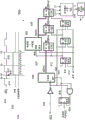
Fig. 2 is a schematic diagram of a system 200 including a master device 202 interfacing with a slave device 204 via a communication link 205 that can implement time stamping and delay triggering in accordance with an embodiment of the present disclosure. For some embodiments, master device 202 may correspond to master device 102 shown in fig. 1, and slave device 204 may correspond to any of slave devices 104 shown in fig. 1. Although one slave device 204 is illustrated in fig. 2, embodiments of the present disclosure support interfacing multiple slave devices 204 to the master device 202. As shown in fig. 2, the communication link 205 may include an SDA bus 206 and an SCL bus 208. As further shown in fig. 2, the master device 202 and the slave device 204 may both drive the SDA bus 206, while only the master device 202 may provide and control a clock signal that may be carried by the SCL bus 208 (hereinafter referred to as SCL clock signal 208). The slave device 204 may communicate with the master device 202 via the SDA bus 206, and the slave device 204 may utilize the SCL clock signal 208 for time stamping and/or synchronization delay triggering of events detected by the slave device 204 (as discussed in more detail below).
In some embodiments, master device 204 may broadcast a Single Data Rate (SDR) command 210 to slave device 204 via SDA bus 206. In one or more embodiments, the SDR command 210 may comprise a time synchronization CCC. After the SDR command 210 is decoded (e.g., by decoding logic 212), slave device 204 may operate in accordance with the decoded SDR command 210. In one embodiment, the time synchronization CCC may be detected at the time tracking/trigger control circuit 214. Based on the detected time sync CCC, a time sync marker (not shown) may be generated by the time tracking/trigger control circuit 214 to begin time synchronization and time tracking until an event occurs and is detected (as discussed in more detail below). As shown in fig. 2, the slave device 204 may be coupled to a sensor 216, the sensor 216 generating a sensor output signal 218 indicative of a measurement of an environmental characteristic. The event detector circuit 220 detects the occurrence of an event from the sensor output signal 218 and generates an event detection signal 222 that switches from a low logic level to a high logic level upon detecting the event.
In some embodiments, the time tracking/trigger control circuit 214 may be configured to time stamp the occurrence of the event (e.g., sensor measurement) 222 with reference to the start of time synchronization, which may be indicated by a time synchronization stamp (not shown). As discussed in more detail below, the time tracking/trigger control circuit 214 may perform time-stamping of the event 222 based at least in part on selected transitions of the SCL clock signal 208 (i.e., the reference clock signal) that may be generated and controlled by the master device 202. The time tracking/trigger control circuit 214 may store a time stamp 224 of the event 222. As shown in fig. 2 and discussed in more detail below, communication logic 226 may read the value of timestamp 224 and provide timestamp value 224 to SDA bus 206 (e.g., when SDA bus 206 has no other traffic). As further shown in fig. 2, communication logic 226 and decoding logic 212 represent an interface 228 that couples slave device 204 to SDA bus 206.
In some embodiments, prior to broadcasting the SDR command 210 with the time-synchronized CCC, the master device 202 may communicate other SDR commands (e.g., via SDA bus 206) to the slave device 204 with delay setting information that determines the time delay for generating a trigger signal by the slave device 204. As shown in fig. 2, the trigger delay setting circuit 230 generates delay setting information 232 that indicates a trigger delay in the form of an SCL clock signal 208 of a number of select transitions to occur between the SDR command 210 with time synchronization CCC and generating a trigger signal at the slave device 204. In one embodiment, the trigger delay setting circuit 230 generates the delay setting information 232 based on an expected frequency change of the SCL clock signal 208 to occur after the SDR command 210 with time synchronization CCC. Information about the expected frequency change of the SCL clock signal 208 is known at the master device 202. The encoder 234 of the master device communication interface 236 encodes the delay setting information 232 within the SDR command 210. An SDR command 210 with encoded delay setting information 232 is then broadcast to one or more slave devices 204 via SDA bus 206 to initiate the delay trigger. As further shown in fig. 2, once the decode logic 212 of the slave device 204 decodes the delay setting information (e.g., coarse delay setting and fine delay setting) provided by the master device 202 within the SDR command 210, and thereafter detects the time synchronization CCC encoded in another SDR command 210, the time tracking/trigger control circuit 214 may be configured to generate the delay trigger signal 238 at a time delay determined based on the provided delay setting information (as discussed in more detail below). In one embodiment, the delayed trigger signal 238 may initiate operation (e.g., measurement) of a peripheral device coupled to the slave device 204, such as operation of an output transducer 240 coupled to the slave device 204.
In some embodiments, the time tracking circuit 242 of the master device 202 illustrated in fig. 2 may be configured to track the actual time from the time synchronization mark generated after the synchronization signal 244. The encoder 234 encodes the synchronization signal 244 to generate an SDR command 210 having a time synchronization CCC, which SDR command 210 may then be broadcast to one or more slave devices 204 via SDA bus 206 to initiate time synchronization. The synchronous CCC broadcast 246 (i.e., the time synchronous CCC) may also be detected within the time tracking circuit 242, and the time tracking circuit 242 may then generate a time synchronization marker indicating the start of tracking the system reference time at the master device 202 based on tracking the number of selected transitions of the SLC clock signal 208.
In some embodiments, counter circuit 248 within time tracking circuit 242 may be configured to keep track of the number of selected transitions (e.g., falling edges) of SCL clock signal 208. For each frequency of the SCL clock signal 208, the number of selected transitions of the SCL signal 208 (e.g., represented as SCL count C0 in fig. 2) may be saved into a latch 250, which latch 250 may be controlled by a frequency Change (COF) signal 252. As discussed in more detail below, SCL count C0 may represent the number of select transitions of SCL clock signal 208 between the time synchronization marker and the last select transition (e.g., falling edge) of SCL clock signal 208 prior to a change in the frequency of SCL clock signal 208. After each frequency change of the SCL clock signal 208, the updated SCL count C0 may be stored in a latch 250 controlled by the COF signal 252. The updated SCL count C0 may indicate the number of select transitions of SCL clock signal 208 between the time synchronization flag and the last select transition of SCL clock signal 208 prior to the change in frequency of SCL clock signal 208. The previous (old) value of SCL count C0 may also be saved in a register file (e.g., a look-up table) 254 after each frequency change of SCL clock signal 208 and based on the corresponding COF signal 252. Accordingly, register file 254 may include different values (e.g., values CNT _1, CNT _2, …, CNT _ N) of SCL count C0 corresponding to N different frequencies of SCL clock signal 208. Each value CNT _ i stored in register file 254 may also be associated with a value Ti encoding a period of each frequency of SCL clock signal 208. Thus, the values of CNT _ i and Ti (i ═ 1, …, N) stored in register file 254 may provide information about the system reference time stamped from the time synchronization.
In some embodiments, the master device 202 may receive information about the timestamp 224 of the event 222 detected at the slave device 204 via the SDA bus 206. The master device 202 may use the information stored in the register file 254 regarding the system reference time tracked from the start of the time synchronization marker to correlate it with the timestamp 224 (e.g., at the actual time calculation circuit 256) to determine the exact global (system) time 258 at which the event 222 occurred. The calculated time 258 represents a global time measured based on a selected transition of the SCL clock signal 208 from the start of the time synchronization mark at the master device 202. In one embodiment, SCL clock signal 208 may be generated at master device 202 by an adjustable clock generator 260, and adjustable clock generator 260 may provide the frequency of SCL clock signal 208 based on an indication 262 (e.g., indication Ti) of the desired period of SCL clock signal 208.
As discussed above, embodiments of the present disclosure support the addition of a new timestamp sync CCC broadcast command to the message protocol. The master device 202 may issue a timestamp synchronization command via the SDA bus 206 to synchronize one or more slave devices 204 coupled to the SDA bus 206 to a particular selected transition (e.g., falling edge) of the clock signal driving the SCL bus. Fig. 3 illustrates waveforms of an example timestamp sync command 300 and signals driving the SDA and SCL buses in relation to the timestamp sync command 300, according to an embodiment of the present disclosure. The timestamp sync command 300 may be initiated by the master device 202 and broadcast to one or more slave devices 204 via SDA bus 206. As shown in fig. 3, the start portion 302 of the timestamp synchronization command 300 may be followed by a broadcast portion 304 indicated with a value of 0x 7E. Toward the end of the broadcast portion 304, the master device may send a write operation ('W') signal to the slave devices, where at least one of the slave devices may respond to the write operation ('W') with an Acknowledgement (ACK) on the SDA bus to acknowledge receipt of the broadcast portion 304 of the time stamp synchronization command 300.
As shown in fig. 3, the SDR command CCC portion 306 of the timestamp synchronization command 300 may follow the broadcast portion 304. The command code 0x28 corresponds to a time stamp synchronization command. A portion 308 (e.g., a 'T' bit) may be associated with a particular signal waveform 310 on the SDA bus. During the time stamping of the 'T' bit of the synchronization command 300, the slave device 204 may detect the time synchronization CCC 312 after a first selected transition (e.g., rising edge) of the SCL clock signal. The next selected transition (e.g., falling edge) of the SCL clock signal may represent the time synchronization mark 314, the time synchronization mark 314 also being detected at the slave device 204. As discussed in more detail below, the time synchronization marker 314 may represent a time when synchronization of one or more slave devices 204 with a system reference time base generated by the master device 202 begins. As further shown in fig. 3, the timestamp sync command 300 may end at the portion 316 that initiates reading of data from the slave device 204 via the SDA bus.
In some embodiments, as discussed in more detail below, the time sync mark 314 provides a way for multiple slave devices to synchronize to time stamp events. The time synchronization marker 314 also allows multiple slave devices to initiate simultaneous operations (e.g., measurements) via a time synchronization trigger. As a result, the need for a side channel between the master and slave devices for synchronizing events may be eliminated. It should be noted that in the case of triggering, no time unit or local clock is of interest, since all slaves are triggered simultaneously.
In some other embodiments, time stamping of events detected at the slave device may be supported based on the time synchronization mark 314. As discussed in more detail below, control circuitry within the slave device may be initialized based on the time synchronization marker 314 and may be configured to track the number of selected transitions of the SCL clock signal. Upon detecting an event, the number of selected transitions of the SCL clock signal in the following may be saved in the local memory of the slave device to be read back by the master device at a later time. The master device generating and controlling the SCL clock signal may also keep track of the number of selected transitions of the SCL clock signal and may correlate its count with the saved timestamp count read back from the slave device in order to determine the global system time at which the event occurred.
Fig. 4 is an example schematic diagram of a circuit 400 for implementing time synchronization at a slave device, such as slave device 204, in accordance with an embodiment of the present disclosure. In some embodiments, the circuit 400 may be part of the time tracking/trigger control circuit 214 illustrated in fig. 2. The flip-flop 420 outputs the sync pulse 402 onto the reset line 404 upon detection of the (time) sync CCC (i.e., upon detection of the rising edge of the pulse 406). Referring back to fig. 2, the pulse 406 detected by the sync CCC may be generated by the decode logic 212 of the slave device 204 upon detection of the time sync command 210. The select transition of the sync pulse 402, which is a falling edge 408 as shown in fig. 4, may represent a time sync mark. Referring back to fig. 3, the time synchronization mark 314 may be aligned with a selected transition of the SCL clock signal during the 'T' bit of the time stamp synchronization command 300 after the time synchronization CCC is detected. Thus, as shown in fig. 4, the time synchronization mark may be aligned with a select transition 410 of the SCL clock signal 412 following the detection of the rising edge of the pulse 406 indicating the synchronized CCC.
In some embodiments, the presence of the synchronization pulse 402 at the reset line 404 may reset the counter 414 to all zeros, as illustrated by the waveform 416 at the output of the counter 414. Counter 414 increments after each selection transition of SCL clock signal 412 (e.g., after each falling edge) after being reset to all zeros. It may be noted that the method presented herein and illustrated in fig. 4 provides a uniform time reference across all slaves including the circuit 400 shown in fig. 4, which is based on the synchronization pulse 402 and a time synchronization mark aligned with a selected transition of the SCL clock signal (which may be controlled by the master).
In some embodiments, a burst oscillator may be employed at the slave device to improve the resolution of the time stamping and delay triggering. Fig. 5 is an example schematic diagram of an oscillator circuit 500 that may be implemented at the slave device 204 for improving resolution of time synchronization in accordance with an embodiment of the present disclosure. In one or more embodiments, oscillator circuit 500 may be part of time tracking/trigger control circuit 214 of slave device 204 shown in fig. 2.
As shown in fig. 5, oscillator circuit 500 may include a burst oscillator 502 and a counter 504. The burst oscillator 502 includes a number of series-connected inverters that generate a high-speed clock signal 506 when an enable signal 508 is at a high logic level. The frequency of the high speed clock signal 506 is higher than the frequency of the SCL clock signal. Upon initiation by the reset signal 510, the counter 504 begins counting select transitions of the high speed clock signal 506. The output F (0) of the burst oscillator 502 and the m-bit output F (1: m) of the counter 504 form the output 512 of the oscillator circuit 500. In one or more embodiments, the burst oscillator 502 may be configured to operate for a limited amount of time sufficient to make a certain number of measurements (e.g., one or two measurements) after an event is detected. Thus, the burst oscillator 502 consumes a limited amount of power.
In one embodiment, some type of sensor (e.g., accelerometer, gyroscope) coupled to the slave device inherently has a relatively stable time base, and may use that time base to provide a clock signal that may be used to improve resolution of time stamping and delay triggering. Other sensors may not have a stable time base and need to employ a local oscillator for generating a local clock signal. In one embodiment, the local oscillator at the slave device may be based on a Phase Locked Loop (PLL) device that uses the SCL clock signal as a reference clock to generate a synchronous and stable local clock having a higher frequency than the SCL clock signal. However, this method has the disadvantage of consuming continuous power and large silicon area.
Fig. 6 is an example schematic diagram of a circuit 600 for implementing time stamping at a slave device 204 according to an embodiment of the present disclosure. The circuit 600 may be part of the time tracking/trigger control circuit 214 of the slave device 204 shown in fig. 2. As shown in fig. 6, circuit 600 may include circuit 400 from fig. 4 and oscillator circuit 500 from fig. 5. In some embodiments, the circuit 600 may be configured to implement time stamping at the slave device 204, and the oscillator circuit 500 is used to increase the resolution of the time stamping when compared to time stamping using only a count of selected transitions of the SCL clock signal.
As discussed above with reference to the circuit 400 illustrated in fig. 4, the synchronization pulse present at the reset line 602 (e.g., the synchronization pulse 402 shown in fig. 4) may be generated upon detection of the (time) synchronization CCC, i.e., upon detection of the rising edge of the pulse 406 shown in fig. 4 at the input 604. The falling edge of the synchronization pulse (e.g., synchronization pulse 402 shown in fig. 4) may represent a time synchronization mark aligned with a selected transition of SCL clock signal 606 (e.g., falling edge 410 shown in fig. 4) during the 'T' bit of a time stamp synchronization command (e.g., SDR time synchronization command 210 broadcast from master device 202 shown in fig. 2, time stamp synchronization command 300 shown in fig. 3) after the synchronization CCC is detected at input 604. The sync pulse present at reset line 602 may reset counter 608 to all zeros. In one embodiment, counter 608 may be the same counter 414 of circuit 400 shown in FIG. 4. The counter 608 may be configured to increment at each selection transition (e.g., falling edge) of the SCL clock signal 606, which may be generated and controlled by a master device (e.g., the master device 102 illustrated in fig. 1, the master device 202 illustrated in fig. 2), and may provide a uniform time reference across all slave devices (e.g., the slave device 104 illustrated in fig. 1, the plurality of slave devices 204 illustrated in fig. 2).
In some embodiments, event 610 may be time stamped based at least in part on value 612 of counter 608. Upon detecting the occurrence of event 610, a value 612 representing the number of select transitions of SCL clock signal 606 between the time synchronization marker and the last select transition 614 of SCL clock signal 606 prior to detecting event 610 may be stored in latch 616 (e.g., value C0 shown in fig. 6 may be stored in latch 616).
In some embodiments, as discussed, oscillator circuit 500 may be used in conjunction with counter 608 to provide finer resolution for time stamping. The oscillator circuit 500, including the burst oscillator 502 from fig. 5, may be configured to generate a periodic oscillator signal having a frequency higher than the frequency of the SCL clock signal 606. As shown in fig. 6, upon detecting an event 610, the flip-flop 618 generates an enable signal 620 that activates the burst oscillator 502 within the oscillator circuit 500. Upon activation based on the enable signal 620, the burst oscillator 502 of the oscillator circuit 500 may generate a high-speed clock signal (oscillator signal) 506, and the counter 504 of the oscillator circuit 500 may keep track of the number of selected transitions (e.g., falling edges) of the oscillator signal 506.
In one or more embodiments, the first selected transition 622 of SCL clock signal 606 following detection of event 610 causes the output of flip-flop 624 to go high, thereby initiating storage of value 626 at the output of oscillator & counter circuit 500 in latch 628. This value is shown as C1. The value of C1 represents a delay in the form of the number of selected transitions of oscillator signal 506 between the detection of event 610 and the first selected transition 622 of SCL clock signal 606 following the detection of event 610.
The next select transition 630 of SCL clock signal 606 after first select transition 622 causes the output of flip-flop 632 to go high. As a result, this initiates the storage of a new value 626 at the output of the oscillator & counter circuit 500 in latch 634. This value is shown as C2. The value of C2 represents a delay in the form of the number of select transitions of oscillator signal 506 between the detection of event 610 and a second select transition 630 of SCL clock signal 606 following the first select transition 622.
In some embodiments, the information regarding the elapsed time between the time sync marker and the detection of the event 610 (i.e., the timestamp of the event 610) may be based on the stored values C0, C1, and C2. In one or more embodiments, the timestamp 224 from fig. 2 may be calculated at the slave device 204 by the timestamp calculation circuit 636 shown in fig. 6 as:

in equation (1), T0 represents the time stamp 224. Information regarding the timestamp of the event 610 may be communicated to the master device 202 via the interface 228 of the slave device 204 when the SDA bus 206 is available. In one embodiment, as shown in fig. 6, the timestamp value T0 defined by equation (1) may also be stored in the delay register 638 before being communicated to the master 202. Delay register 638 may hold timestamp value T0 until SDA bus 206 becomes available.
Fig. 7 is an example diagram 700 of times at which events are captured and read by a master device 702 from multiple slave devices 704 and 706, according to an embodiment of the disclosure. Master device 702 may correspond to master device 202 shown in fig. 2, and each of slave devices 704 and 706 may correspond to slave device 204 shown in fig. 2. As shown in fig. 7, the master device 702 may broadcast a time synchronization CCC 708 to the slave devices 704, 706. The slave devices 704, 706 may track the time delay 710, 712 between the time synchronization marker (not shown in fig. 7) generated when the sync CCC 708 is detected at the slave devices 704, 706 and the detection of an event at each slave device. When event 714 is detected at slave device 704 and event 716 is detected at slave device 706, a time delay, represented as the number of select transitions (not shown in fig. 7) of the SCL clock signal tracked at each slave device, is latched, i.e., the event is time stamped in each slave device and stored in a delay register. As shown in fig. 7, the slave device 704 may store the tracked delay 710 as a timestamp of the event 714 into a delay register 718; slave device 706 may store tracked delay 712 as a timestamp of event 716 into delay register 720. In one or more embodiments, the delay register 718 of the slave device 704 and the delay register 720 of the slave device 706 may correspond to the delay register 638 illustrated in fig. 6.
In some embodiments, the slave device 204 shown in fig. 2 may need to wait for a bus idle condition on the SDA bus 206 before the slave device can initiate an interrupt to the master device 202 shown in fig. 2. As shown in fig. 7, the slave devices 704, 706 may need to wait until the traffic 722 on the SDA bus completes. The slave device 706 may then initiate an in-band interrupt (IBI)724 that signals the master device 702 that the timestamp 712 of the event 716 is available for reading by the master device 702. Upon receiving the IBI 724, the master device 702 may send a request 726 to the slave device 706 via the SDA bus, the request 726 requesting to read information about the timestamp 712 of the event 716 stored in the delay register 720 of the slave device 706. Upon receiving the request 726, the slave device 706 may read 728 the timestamp 712 from the delay register 720 and provide information regarding the timestamp 712 of the event 716 to the master device 702 via the SDA bus. After that, the master device 702 may initiate another read 730 of the delay register 720 of the slave device 704, the delay register 720 storing information about the timestamp 710 of the event 714. Information regarding the timestamp 710 of the event 714 may then be provided to the master device 702 via the SDA bus.
In the illustrative embodiment shown in fig. 7, slave device 706 may have a higher priority than slave device 704. Although the slave device 704 may also initiate an IBI, in this case the slave device 704 does not have an opportunity to do so because the master device 702 decides to automatically read the timestamp 710 of the event 714 in response to the IBI 724 received from the slave device 706. It should also be noted that due to traffic 722 after synchronizing CCC 708, the SCL clock signal (not shown in fig. 7) may be continuously switched before and after the detected events 714, 716, thereby providing a continuous time basis for reference by the slave devices 704, 706.
Fig. 8 is an exemplary graph 800 of times at which events are captured and read from multiple slave devices 804 and 806 by a master device 802 and a monitoring device 808, according to an embodiment of the disclosure. In some embodiments, the monitoring device 808 may interface with the slave devices 804 and 806 via the SDA bus and the SCL bus. Unlike the master device 802, the monitoring device 808 neither issues any commands nor generates/controls any clock signals. Instead, the monitoring device 808 may simply monitor traffic on the SDA bus and collect corresponding information communicated by the master device 802 and/or slave devices 804, 806 on the SDA bus. The master device 802 may correspond to the master device 202 from fig. 2, and each slave device 804, 806 may correspond to the slave device 204 from fig. 2.
As shown in fig. 8, the master device 802 may broadcast a time sync CCC 810 to the slave devices 804, 806, and the slave devices 804, 806 may track time delays 812 and 814 between a time sync marker (not shown in fig. 8) generated when the sync CCC 810 is detected at the slave devices 804, 806 and the detection of an event at each slave device. The synchronous CCC 810 may also be detected by the monitoring device 808. When an event 816 is detected at the slave device 804 and an event 818 is detected at the slave device 806, the time delay tracked at each slave device is latched, i.e., the event is time stamped in each slave device and stored in a delay register. As shown in fig. 8, the slave device 804 may store the tracked delay 812 between the time synchronization marker and the detected event 816 in a delay register 820; the slave device 806 may store the tracked delay 814 between the time synchronization marker and the event 818 in the delay register 822. In one or more embodiments, the delay register 820 of the slave device 804 and the delay register 822 of the slave device 806 may correspond to the delay register 638 illustrated in fig. 6.
As further shown in fig. 8, other traffic 824 may be provided by the master device 802 on the SDA bus. The same traffic 824 may also be monitored by the monitoring device 808. In some embodiments, each slave device may need to wait for a bus idle condition on the SDA bus before the slave device can initiate an interrupt to the master device. As shown in fig. 8, the slave devices 804, 806 may need to wait until the traffic 824 of the SDA bus is complete. The slave device 806 may then initiate an IBI, which signals 826 the timestamp 814 of the event 818 available to be read via the SDA bus. The same interrupt 826 sent via the SDA bus may be received by both the master device 802 and the monitoring device 808. Upon receiving the interrupt 826, the master device 802 may provide a request 828 to the slave device 806 with an address of the slave device 806, the request 828 requesting to read information about the timestamp 814 of the event 818 stored in the delay register 822 of the slave device 806. The request 828 including the address of the slave device 806 may also be received by the monitoring device 808.
Upon receiving the request 828, the slave device 806 may read 830 the timestamp 814 from the delay register 822 and provide information about the timestamp 814 of the event 818 to the master device 802 via the SDA bus. Meanwhile, since information about the timestamp 814 of the event 818 is available at the SDA bus, the monitoring device 808 may also obtain the timestamp 814 of the event 818. After that, the master device 802 may initiate another read 834 of the slave delay register 820 by sending a request 832 with the address of the slave device 804, the delay register 820 storing information about the timestamp 812 of the event 816. The address 832 of the slave device 804 may also be received by the monitoring device 808 monitoring all traffic on the SDA bus. Information regarding the timestamp 812 of the event 816 may then be provided to the master device 802 and the monitoring device 808 via the SDA bus. As discussed in more detail herein with respect to fig. 2 and 12, upon receiving the timestamp data 812 and 814 from the slave devices 804 and 806, respectively, the master device 802 calculates the times of the events 816 and 818 with reference to a global system reference clock signal (i.e., SCL clock signal) (not shown in fig. 8) generated and controlled by the master device 802.
In some embodiments, the master device 802 is not capable of processing the timestamp data 812, 814, i.e., the master device 802 does not support converting the timestamp data 812, 814 to the actual time of the event referencing the global system reference clock signal. In this case, the monitoring device 808 may be configured to process the processing of the timestamp data 812, 814 received from the slave devices 804, 806, thereby allowing the use of master devices that do not support timestamp. In this configuration, the master device 802 may still control the SDA bus and SCL bus, as well as handle read/write/interrupts from/to the slave devices 804, 806, as discussed above. However, the master device 802 does not deal with the complexity of the time stamp. Instead, the monitoring device 808 is configured to convert the received timestamp data 812, 814 into a time of an event 816, 818 referenced to the global system reference clock signal. As discussed in more detail with respect to fig. 2 and 12, the monitoring device 808 is configured to keep track of and time transitions of the SCL clock signal relative to its own accurate time base in the same manner that the master device 802 will do.
When the slave device 806 initiates the IBI 826 by pulling down the SDA bus during a bus idle state after the traffic 824 is complete, the master device 802 responds by toggling the SCL clock signal and initiates a read back of the slave device to the timestamp information 814 by sending a request 828. However, the master device 802 may ignore the received timestamp information 814. Instead, the master device 802 may rely on the monitoring device 808, the monitoring device 808 being configured to also read the same timestamp data 814 and use the timestamp 814 to calculate the actual time of the event 818 detected at the slave device 806. Similarly, the monitoring device 808 utilizes the timestamp 812 received from the slave device 804 and calculates the time of the event 816 detected at the slave device 804. At a later time, the monitoring device 808 may send information regarding the time of the event 816, 818 to the master device 802.
In the illustrative embodiment shown in fig. 8, slave device 806 may have a higher priority than slave device 804. Although the slave device 804 may also initiate an IBI, the slave device 804 does not have an opportunity to do so in this case because the master device 802 decides to automatically read the timestamp 812 of the event 816 in response to the IBI 826 received from the slave device 806. It should be noted that due to the traffic 824 after synchronizing the CCC 810, the SCL clock signal (not shown in fig. 8) may be continuously switched before and after the detected events 816, 818, thereby providing a continuous time basis for reference by the slave devices 804, 806.
Fig. 9 is an example schematic diagram of a circuit 900 for implementing time stamping at a slave device (e.g., slave device 204 shown in fig. 2) that does not have oscillator circuit 500 from fig. 5 shown as part of time stamping circuit 600 in fig. 6, according to an embodiment of the present disclosure. The circuit 900 may be part of the time tracking/trigger control circuit 214 of the slave device 204 shown in fig. 2.
As discussed above with reference to the circuit 400 illustrated in fig. 4, the synchronization pulse 402 present at the reset line 902 may be generated upon detection of the (time) synchronization CCC, i.e., upon detection of the rising edge of the pulse 406 shown in fig. 4 at the input 904. The falling edge of the synchronization pulse 402 may represent a time synchronization mark that is aligned with a select transition 410 of the SCL clock signal 906 during the 'T' bit of a time stamp synchronization command (e.g., the SDR time synchronization command 210 broadcast from the master device 202 shown in fig. 2, the time stamp synchronization command 300 shown in fig. 3) after the synchronization CCC is detected at the input 904. The sync pulse present at the reset line 902 may reset the counter 908 to all zeros. Counter 908 may correspond to counter 414 of circuit 400 shown in fig. 4. Counter 908 may be configured to increment at each selection transition of SCL clock signal 906 and may provide a uniform time reference across all slaves while SCL clock signal 906 may be generated and controlled by the master.
In some embodiments, the event 910 may be time stamped based at least in part on the value 912 of the counter 908. Upon detection of event 910, a value 912 may be stored in latch 914, the value 912 representing the number of select transitions of SCL clock signal 906 between the time synchronization marker and the last select transition of SCL clock signal 906 before detection of event 910. As shown in fig. 9, a value C0 representing the number of selected transitions of SCL clock signal 906 between the time synchronization marker and the detection of event 910 is stored in latch 914.
Since the oscillator circuit 500 from fig. 5 including the burst oscillator 502 is not included in the circuit 900 illustrated in fig. 9, the values of C1 and C2 associated with the finer resolution of the time stamps are placeholders and are set to zero. After reading the time stamp data 224 associated with the time of the event 910 given by the value of C0 stored in the latch 914, the master device 202 illustrated in fig. 2 may convert the value of C0+1 and the value of C0+2 into system reference times for each value, i.e., into actual times T1 and T2, respectively, through the actual time calculation unit 256. In some embodiments, the value of C0+1 represents the number of select transitions of SCL clock signal 906 between the time synchronization mark and the first select transition of SCL clock signal 906 after event 910, and the value of C0+2 represents the number of select transitions of SCL clock signal 906 between the time synchronization mark and the second select transition of SCL clock signal 906 after event 910. The master device 202 may then determine the system reference (actual) time T of the event 910 along with T1 and T2. Therefore, the temperature of the molten metal is controlled,

in the illustrative embodiment shown in fig. 9, the values of C1 and C2 are both set to zero, and the actual time T of the event 910 may be determined based solely on the value of C0+1, i.e., the actual time T of the event 910 may be equal to T1.
According to embodiments of the present disclosure, as discussed above, multiple slave devices may initiate simultaneous operations (e.g., measurements) based on time-synchronized triggers controlled by the master device via the SDA bus. Based on this approach, the extra communication channel between the master and slave devices can be eliminated. Embodiments of the present disclosure support the use of time synchronization commands broadcast by a master device that can start a timer at each slave device that triggers an event (e.g., a measurement) at the end of a predetermined time period. In one or more embodiments, the time delay for triggering an event at each slave device may be set by a command communicated by the master device via the SDA bus, which may precede the time synchronization command.
Fig. 10 is an example schematic diagram of a circuit 1000 for implementing delay triggering at the slave device 204 illustrated in fig. 2, in accordance with an embodiment of the present disclosure. The circuit 1000 may be part of the time tracking/trigger control circuit 214 of the slave device 204 shown in fig. 2. In some embodiments, the master device 202 illustrated in fig. 2 may control the exact time of the trigger generated at each slave device 204.
When the (time) sync CCC is detected at input 1004 (i.e., when a time sync command is detected), the flip-flop 1040 generates a sync pulse on the reset line 1002. The falling edge of the synchronization pulse may represent a time synchronization mark 1006, the time synchronization mark 1006 aligned with a selected transition of the SCL clock signal 1008 during the 'T' bit of a time synchronization command (e.g., the SDR time synchronization command 210 broadcast from the master device 202 shown in fig. 2) after the time synchronization command is detected at the input 1004. The sync pulse present at the reset line 1002 may reset the counter 1010 to all zeros. In one embodiment, the counter 1010 may correspond to the counter 414 of the circuit 400 shown in fig. 4. Counter 1010 increments at each selected transition of SCL clock signal 1010, and may provide a uniform time reference across all slave devices 204, where SCL clock signal 1008 may be generated and controlled by master device 202.
The circuit 1000 illustrated in fig. 10 may be generally configured to track a number of select transitions of the SCL clock signal 1008 after detecting the time synchronization command, and to generate the trigger signal in response to the number of select transitions of the SCL clock signal 1008 reaching a delay setting, indicated by delay setting information 1012, which delay setting information 1012 may be provided by the master device 202 into the delay register 1014. In some embodiments, the delay setting information 1012 may include coarse delay setting information 1016 and fine delay setting information 1018, which may be set by the master device 202 in a command communicated prior to broadcasting the time synchronization command via the SDA bus. The coarse delay setting information 1016 indicates a trigger delay in the form of a number of selected transitions of the SCL clock signal 1008 to occur between the time synchronization marker 1006 and the generation of the trigger signal. As shown in fig. 10, comparator 1020 may be configured to compare coarse delay setting information 1016 to a value 1022 of counter 1010, value 1022 representing a number of selected transitions of SCL clock signal 1008 that occur after time synchronization marker 1006. When the value 1022 of counter 1010 equals the coarse delay setting information 1016 and the number of tracked selected transitions of SCL clock signal 1008 reaches the coarse delay setting information 1016, the output of comparator 1024 becomes a logic '1'. As a result, the flip-flop 1050 causes the enable signal 1026 to become a logic '1' and enables the oscillator and counter circuit 1028 to operate. Oscillator and counter circuit 1028 can be used in conjunction with counter 1010 and comparator 1024 to provide finer resolution for delayed triggering.
For some embodiments, the oscillator and counter circuit 1028 may correspond to the oscillator circuit 500 illustrated in fig. 5, including the burst oscillator 502 and the counter 504. When enabled by the enable signal 1026, the oscillator and counter circuit 1028 internally generates a burst oscillator signal 1030 having a frequency higher than the frequency of the SCL clock signal 1008. As shown in fig. 10, after the oscillator and counter circuit 1028 is activated by the enable signal 1026, a burst oscillator within the oscillator and counter circuit 1028 may generate the burst oscillator signal 1030, while a counter within the oscillator and counter circuit 1028 may keep track of the number of selected transitions of the burst oscillator signal 1030. The fine delay setting information 1018 indicates a trigger delay in the form of a number of selected transitions of the burst oscillator signal 1030 to occur between the enable signal 1026 and the generation of the trigger signal. Once the number of selected transitions of the burst oscillator signal 1030, represented by the signal 1032 at the output of the oscillator and counter circuit 1028, reaches the fine delay setting 1018, the comparator 1034 causes the logic level of the trigger signal 1036 to become a logic "1". The trigger signal 1036 switches logic states at the exact time controlled by the master device 202 based on the coarse and fine delay setting information. The trigger signal 1036 generated by the circuit 1000 illustrated in fig. 10 may correspond to the delayed trigger signal 238 generated by the time tracking/trigger control circuit 214 of the slave device 204 shown in fig. 2. At the exact moment controlled by the master device 202, the delayed trigger signal 238 may initiate operation of a transducer 240 coupled to the slave device 204.
Fig. 11 is an example diagram 1100 of the time of events at multiple slave devices controlled by a master device according to an embodiment of the disclosure. As shown in fig. 11, master device 1102 may provide delay setting information to slave devices 1104 and 1106, i.e., delay setting information 1108 may be stored at delay register 1110 of slave device 1104 and delay setting information 1112 may be stored at delay register 1114 of slave device 1106. Delay register 1110 of slave device 1104 and delay register 1114 of slave device 1106 may correspond to delay register 1014 shown in fig. 10. In some embodiments, as discussed, the delay setting information 1108 and 1112 may be communicated to the slave devices 1104 and 1106 via SDR commands sent from the master device 1102 via the SDA bus. The master device 1102 may correspond to the master device 202 from fig. 2, and each slave device 1104, 1106 may correspond to the slave device 204 from fig. 2.
As further shown in fig. 11, after communicating the delay setting information 1108 and 1112, the master device 1102 may broadcast a time synchronization command (sync CCC 1116) via the SDA bus. Upon detection of the sync CCC 1116 at the slave devices 1104 and 1106, a time sync marker (not shown in fig. 11) may be generated at each slave device, i.e., the slave devices 1104 and 1106 may be synchronized by clearing their respective counters. Starting from the time synchronization mark, the slaves 1104 and 1106 may track a reference time, which may be provided by the master 1102 via an SCL clock signal. When the time tracked at the slave device 1104 reaches the delay setting information 1108, the slave device 1104 may generate a trigger in the form of a trigger event 1118, which trigger event 1118 may be delayed from the time synchronization marker by a particular reference time 1120. Similarly, when the time tracked at the slave device 1106 reaches the delay setting information 1112, the slave device 1106 may generate a trigger in the form of a trigger event 1122, which trigger event 1122 may be delayed from the time synchronization marker by a particular reference time 1124.
In some embodiments, as discussed, the master device 202 illustrated in fig. 2 may track the system reference time from the time synchronization marker indicated by the time synchronization command in order to convert the time stamp of the event detected at the slave device 204 to a system (actual) time that references the global clock signal generated and controlled by the master device 202. Fig. 12 is an example schematic diagram of a circuit 1200 implemented at the master device 202 for supporting time stamping according to an embodiment of the present disclosure. The circuit 1200 illustrated in fig. 12 may correspond to the time tracking circuit 234 of the master device 202 shown in fig. 2.
The flip-flop 1202 generates a sync pulse on the reset line 1204 when the synchronous CCC broadcast is indicated by a signal at the input 1206 having a high logic level. The falling edge of the synchronization pulse may represent a time synchronization mark that is aligned with a selected transition of SCL clock signal 1208 during the 'T' bit of the time synchronization command detected at input 1206. The sync pulse present at reset line 1204 may reset counter 1210 to all zeros. The counter 1210 may correspond to the counter circuit 248 of the master device 202 shown in fig. 2. Counter 1210 increments at each selected transition of SCL clock signal 1208 and may provide a uniform time reference between the master device and all slave devices. In one embodiment, when the master device controls the SCL bus (e.g., as in SDR and Double Data Rate (DDR) modes), SCL clock signal 1208 may be derived from the reference clock by clock generator 260 from fig. 2 and controlled by master device 202.
In some embodiments, the change in frequency of SCL clock signal 1208 may be stamped using the value 1212 of counter 1210. Once a frequency Change (COF) signal 1214, indicating a change in the frequency of the SCL clock signal 1208, becomes a logic '1', the value 1212 of the counter 1210 may be stored into the latch 1216, indicated as value C0 in fig. 12. In one embodiment, the value of C0 represents the number of select transitions of SCL clock signal 1208 between the time synchronization mark and the last select transition of SCL clock signal 1208 before the first frequency change of SCL clock signal 1208. Referring back to fig. 2, the value C0 stored into latch 1216 in fig. 12 may correspond to the SCL count C0 stored in latch 250 of master 202 when the COF signal 252 goes high.
In some embodiments, the register or lookup table 1218 may store information related to different periods associated with different frequencies of the SCL clock signal 1208. For example, as shown in fig. 12, bit T (1,0) may encode the duration of a period when the frequency of SCL clock signal 1208 is 12 MHz; bit T (0,1) may encode the duration of a period when the frequency of SCL clock signal 1208 is 1 MHz; and bit T (0,0) may encode the duration of a cycle when SCL clock signal 1208 has a frequency of 400 KHz. The value 1220 encoded by bits T (0: m) at the output of register 1218 may be used in conjunction with the value of C0 stored in latch 1216 to provide a relationship between the number of selected transitions of SCL clock signal 1208 and the actual time reference. Once the COF signal 1214, which indicates a change in the frequency of the SCL clock signal 1208, becomes a logical '1', the value 1220 encoded by the bits T (0: m) at the output of the register 1218 may be stored into the latch 1222, indicated as the value C1. Thus, the value of C1 may represent the period of SCL clock signal 1208 prior to a change in the frequency of SCL clock signal 1208. The latched values of C0 and C1 may provide information about the system time reference between the time sync mark and the COF.
In some embodiments, as shown in fig. 12, when a value 1212 indicating the number of selected transitions of SCL clock signal 1208 between the time synchronization flag and the change in frequency of SCL clock signal 1208 and a value 1220 representing the encoded period of the frequency of SCL clock signal 1208 prior to the change in frequency are stored as values C0 and C1, respectively, the next selected transition of SCL clock signal 1208 may cause flip-flop 1224 to generate an Interrupt (INT) signal 1226, initiating storage of values C0 and C1 into a buffer or register file. After that, a clear signal 1228 may be pulsed, which may reset latches 1216 and 1222, i.e., the latched values C0 and C1 are cleared after being stored into a buffer or register file based on INT signal 1226. Referring back to fig. 2, the values of C0 and C1 stored into the cache or register file may correspond to the CNT _1 and T1 values stored in the register file 254 of the master 202 shown in fig. 2 when the COF signal 252 goes high.
Referring back to fig. 12, after the latches 1216, 1222 are reset, the circuit 1200 may continue to track the number of selected transitions of the SCL clock signal 1208 after the first frequency change of the SCL clock signal 1208 until the next frequency change of the SCL clock signal 1208. The latched values C0 and C1 in fig. 12 may provide information about the reference time between the time synchronization mark and this next frequency change of the SCL clock signal 1208 indicated by the COF signal 1214. In this manner, the master device 202 in fig. 2 may track the reference time based on the SCL clock signal 1208 generated and controlled by the master device 202 starting at the time synchronization marker and correlate it with the timestamp of the event detected at the slave device 204 using this reference time information to calculate the actual time of the reference SCL clock signal 1208 for the occurrence of the event detected at the slave device 204.
From the time of synchronization represented by the time synchronization mark, master device 202 stores the time of the time synchronization mark and counts each selected transition of SCL clock signal 1208 through counter 1210. The master device 202 stores in latches 1222 and 1216 a metric 1220 (i.e., value C1) representative of the frequency of the SCL clock signal 1208 and a count 1212 (i.e., value C0) of selected transitions of the SCL clock signal 1208 occurring at changes in the frequency of the SCL clock signal 1208 indicated by the COF signal 1214. After INT1226 is enabled by COF signal 1214, the stored values of C0 and C1 may be transferred from latches 1216, 1222 into a cache or register file. Referring back to fig. 2, the values of C0 and C1 transferred into the cache or register file may correspond to CNT _ i and Ti values, respectively, which are stored in the register file 254 of the master 202 whenever the COF signal 252 goes high, providing reference time information. In some embodiments, as discussed, the master device 202 may receive a timestamp 224 of the event 222 detected at the slave device 204 via the SDA bus 206. Master device 202 may use the reference time information, i.e., CNT _ i and Ti values, stored in register file 254 to reconstruct the time of any selected transition of the SCL clock signal without actually storing the time of each such transition. When the master device 202 receives the SCL clock signal count or the timestamp 224 of the event 222 detected at the slave device 204, the master device 202 correlates the timestamp 224 with the reference time information of the register file 254 at the actual time calculation unit 256 to determine the exact time 258 of the event 222 relative to the system reference clock.
Fig. 13 is a diagram 1300 illustrating a method performed at the master device 202 illustrated in fig. 2 for time stamping changes in an SCL clock signal, which may be performed by the circuit 1200 in fig. 12, in accordance with an embodiment of the present disclosure. As shown in fig. 13, the SCL clock signal 1302 driving the SCL bus may change its frequency, which may be controlled by the master device 202. Additionally, SCL clock signal 1302 may have no transitions for a certain period of time, which corresponds to a bus idle condition. Thus, as shown in fig. 13, SCL clock signal 1302 is not periodic for a certain period of time during a bus idle condition, and SCL clock signal 1302 may become periodic again. As discussed above with respect to the circuit 1200 illustrated in fig. 12, the master device 202 may time stamp the last selected transition of the SCL clock signal 1302 prior to the change in frequency of the SCL clock signal 1302. As shown in fig. 13, the selected last transition 1304 associated with the previous clock frequency 1306 of SCL clock signal 1302 may be time stamped relative to a time synchronization mark (not shown). After that, the last selected transition of SCL clock signal 1302 for the next clock frequency 1308 is also time stamped, i.e., the last high-to-low transition 1310 of SCL clock signal 1302 prior to bus idle condition 1312 is time stamped. Time stamp 1310 together with time stamp 1304 indicates the time between two successive frequency changes of SCL clock signal 1302. It should be noted that bus free condition 1312 when SCL clock signal 1302 is not periodic may also be considered a change in frequency of SCL clock signal 1302 because the frequency of SCL clock signal 1302 actually changes from non-zero frequency 1308 to zero. Thus, the high-to-low transition 1314 of SCL clock signal 1302 when transitioning from bus idle condition 1312 to new clock frequency 1316 is also time stamped. The time stamp 1314, along with the time stamp 1310, indicates the duration of the bus idle condition 1312.
In some embodiments, as discussed, the master device 202 illustrated in fig. 2 may use select transitions of the time stamps of SCL clock signal 1302 (e.g., time-stamped transitions 1304, 1310, 1314, etc.) to determine a system reference time for any time-stamped event that the slave device 204 has detected. The time stamps 1304, 1310, 1314 may correspond to the values CNT _ i stored in the register file 254 of the master device 202. The master device 204 may correlate the timestamp 224 of the event 222 detected at the slave device 204 with the transitions 1304, 1310, 1314 of the timestamps of the SCL clock signal including information about the period Ti of the SCL clock signal and determine the system reference time 258 of the event by the actual time calculation circuit 256.
Embodiments of the present disclosure relate to a method for translating a system time base at a master device to a local time base at a slave device for time stamping and delayed triggering. Referring back to fig. 2, the master device 202 may be configured to generate a reference SCL clock signal 208, the reference SCL clock signal 208 also being available at one or more slave devices 204. In one or more embodiments, the reference SCL clock signal 208 may have a particular resolution and may be translatable to a system time. Master device 202 may then provide a synchronization indication on SDA bus 206 in the form of time synchronization commands 210 and 300 shown in fig. 2 and 3. By providing a synchronization indication, the master device 202 may also set a reference point on the SDA bus 206, which may correspond to a selected transition of the reference SCL clock signal 208 during the time synchronization command. A reference point provided by the master device 202 may be received at each slave device 204 as a time synchronization marker aligned with a selected transition of the reference SCL clock signal 208. In some embodiments, as discussed, each slave device 204 may track the amount of time that has elapsed in a local time reference in response to receiving the reference point. In response to detecting an event at the slave device 204, an indication of the amount of local time that has elapsed when the event was detected may be loaded into a register and/or may be sent to SDA bus 206. In addition, based on the reference point provided by the master device 202 and the reference SCL clock signal 208, each slave device 204 may generate a trigger signal at a time instant that is directly controlled by the master device 202 and referenced based on a system time base.
Embodiments of the present disclosure also relate to a method for translating a local time base at a slave device to a system time base at a master device for time stamping. One or more slave devices 204 may monitor for the occurrence of an event. As discussed, at each slave device 204, the occurrence of an event may be tagged on a local time basis, and the timestamp of the event may be latched at the slave device 204. Before beginning to monitor for the occurrence of an event, each slave device 204 may receive a reference point signal in the form of a time sync marker from the master device 202 via SDA bus 206. The time synchronization marker may be based on a reference clock (such as SCL clock signal 208) generated and controlled at the master device 202, and may thus be translatable to a system-wide time base. At each slave device 204, a delay between the time when the time synchronization marker is received at that slave device 204 and the time when the occurrence of the event is detected on a local time basis may be determined. The delay corresponds to the time of the event in the local time base and may be reported to the master device 202. In some embodiments, as discussed, the master device 202 may determine a respective time of occurrence of each of the events at the slave device 204 in a system-wide time base.
Fig. 14 is a flow chart illustrating a method 1400 for time stamping that may be performed at the master device 202 illustrated in fig. 2 in accordance with an embodiment of the present disclosure.
The operations of the method 1400 may begin with the master device 202 generating 1402 a clock signal (e.g., the SCL clock signal 208) and a synchronization command (such as the time synchronization command 210).
The master device 202 transmits 1404 a clock signal and a synchronization command via a communication link, such as the communication link 205 illustrated in fig. 2 that includes the SCL line 208 and the SDA line 206.
The master device 202 receives 1406 timestamp information (e.g., timestamp 224) via the communication link, the timestamp information indicating a number of selected transitions of the clock signal that elapse between the synchronization command and a time when the event was detected at the slave device (e.g., event 222 was detected at slave device 204).
The time tracking circuit 234 of the master device 202, shown in greater detail as circuit 1200 in fig. 12, tracks 1408 a count of selected transitions of the clock signal between the synchronous command and a change in frequency of the clock signal that occurs after the synchronous command.
The actual time calculation unit 256 of the master device 202 determines 1410 a time of the event detected at the slave device based on the timestamp information and the count of selected transitions of the clock signal.
Fig. 15 is a flow diagram illustrating a method 1500 for delayed triggering that may be performed at the slave device 204 illustrated in fig. 2 in accordance with an embodiment of the present disclosure.
The operations of method 1500 may begin with: via a communication link carrying a clock signal (e.g., SCL clock signal 208), the slave device 204 receives 1502 a synchronization command (e.g., time synchronization command 210) and delay setting information, which may be provided by the SDR command 210 generated by the master device 202 prior to the time synchronization command. In some embodiments, as discussed, the communication link may correspond to the communication link 205 including the SDA line 206 and the SCL line 208.
The time tracking/trigger control circuit 214 of the slave device 202, shown in greater detail as circuit 1000 in fig. 10, tracks 1504 the number of selected transitions of the clock signal (e.g., falling edges of the SCL clock signal 208) following the synchronization command.
In response to the number of selection transitions reaching the delay setting indicated by the delay setting information, the slave device 204 generates 1506 a trigger signal (such as the delay trigger 238).
Fig. 16 is a flow diagram illustrating a method 1600 for delayed triggering that may be performed at the master device 202 illustrated in fig. 2, in accordance with an embodiment of the present disclosure.
The operations of the method 1600 may begin with the master device 202 transmitting 1602 a clock signal (e.g., SCL clock signal 208) and a synchronization command (e.g., time synchronization command 210) via a communication link. In some embodiments, as discussed, the communication link may correspond to the communication link 205 including the SDA line 206 and the SCL line 208.
The master device 202 transmits 1604 delay setting information indicating a number of selective transitions of the clock signal to occur between the synchronization command and generation of a trigger signal (e.g., delay trigger 238) at one or more slave devices 204 coupled to the communication link. In some embodiments, as discussed, the delay setting information may include coarse delay setting information and fine delay setting information that are located in the SDR command 210 generated by the master device 202 prior to the synchronization command.
The foregoing description of embodiments of the present disclosure has been presented for purposes of illustration; it is not intended to be exhaustive or to limit the disclosure to the precise form disclosed. One skilled in the relevant art will recognize, in view of the above disclosure, that many modifications and variations are possible.
Portions of the present specification describe embodiments of the disclosure in terms of algorithms and symbolic representations of operations on information. These algorithmic descriptions and representations are the means used by those skilled in the data processing arts to convey the substance of their work effectively to others skilled in the art. When described functionally, computationally, or logically, these operations are understood to be implemented by computer programs or equivalent circuits, microcode, or the like. In addition, it has also proven convenient at times, to refer to these arrangements of operations as modules, without loss of generality. The described operations and their associated modules may be implemented in software, firmware, hardware, or any combination thereof.
Any of the steps, operations, or processes described herein may be performed or implemented using one or more hardware or software modules, alone or in combination with other devices. In one embodiment, the software modules are implemented using a computer program product comprising a computer readable medium having computer program code embodied therewith, the computer program code executable by a computer processor to perform any or all of the steps, operations, or processes described.
Embodiments of the present disclosure may also relate to an apparatus for performing the operations herein. This apparatus may be specially constructed for the required purposes, and/or it may comprise a general purpose computing device selectively activated or reconfigured by a computer program stored in the computer. Such a computer program may be stored in a non-transitory tangible computer readable storage medium or any type of medium suitable for storing electronic instructions, which may be coupled to a computer system bus. In addition, any computing system referenced in this specification may include a single processor or, alternatively, may be an architecture that employs multiple processor designs for increased computing power.
Finally, the language used in the specification has been principally selected for readability and instructional purposes, and may not have been selected to delineate or circumscribe the inventive subject matter. Therefore, it is intended that the scope of the disclosure be limited not by this detailed description, but rather by any claims that issue on an application-based basis. Accordingly, the disclosure of the embodiments is intended to be illustrative, but not limiting, of the scope of the disclosure, which is set forth in the following claims.
Claims (26)
1. A system for low speed bus time stamping, the system comprising:
a master device coupled to a communication link, the master device to transmit a clock signal and a synchronization command via the communication link; and
one or more slave devices coupled to the communication link, each slave device to:
tracking a number of selected transitions of the clock signal between the synchronization command and an event detected at the slave device, and
generating information on an elapsed time between the synchronization command and the event detected at the slave device, the information based on the number of selected transitions of the clock signal tracked at the slave device,
the master device is to obtain the information about the elapsed time and to derive a time at which the event was detected at the slave device based on the information.
2. The system of claim 1, wherein the master device is to receive the information regarding the elapsed time and to determine the time at which the event was detected at the slave device based on the received information regarding the elapsed time and a number of selected transitions of the clock signal that occur between changes in frequency of the clock signal tracked at the master device.
3. The system of claim 1, wherein the communication link comprises a single clock line carrying the clock signal and a single data line carrying the synchronization command.
4. The system of claim 1, wherein:
the one or more slave devices include a plurality of slave devices, and
each slave device of the plurality of slave devices is coupled to a corresponding sensor, and the event detected at a slave device corresponds to a detection of a physical phenomenon by the corresponding sensor.
5. The system of claim 1, wherein:
each slave device includes an oscillator circuit for generating an oscillator signal having a frequency higher than that of the clock signal, and
each slave device is to count a number of select transitions of the oscillator signal that occur after the event is detected at the slave device, and to generate the information about the elapsed time based on the number of select transitions of the oscillator signal.
6. The system of claim 1, wherein:
the slave device to generate an interrupt in response to detecting the event at the slave device;
the master device to generate a request to read the information about the elapsed time from a register of the slave device in response to the interrupt;
the slave device to generate the information regarding the elapsed time for the master device in response to the request; and is
The master device is to store the information regarding the elapsed time obtained from the slave device via the communication link in a register of the master device.
7. The system of claim 1, wherein:
the slave device to generate an interrupt in response to detecting the event at the slave device;
the master device to generate, in response to the interrupt, a request to read the information about the elapsed time from a register of the slave device and to generate another request to read timestamp information from a register of another slave device of the one or more slave devices;
the slave device to generate the information regarding the elapsed time for the master device in response to the request;
the further slave device is to generate the timestamp information for the master device in response to the further request;
the master device to store the information regarding the elapsed time obtained from the slave device via the communication link in a register of the master device; and is
The master device is to store the timestamp information obtained from the other slave device via the communication link in another register of the master device.
8. The system of claim 7, further comprising:
a monitoring device coupled to the communication link, the monitoring device to:
receiving the information regarding the elapsed time and storing the information regarding the elapsed time in a register of the monitoring device;
receiving the time stamp information and storing the time stamp information in another register of the monitoring device; and is
Transmitting the information on the elapsed time and the timestamp information to the master device.
9. A master device, comprising:
an interface circuit for coupling to a communication link, the interface circuit to:
transmitting a clock signal and a synchronization command via the communication link; and
receiving first timestamp information via the communication link, the first timestamp information indicating a number of selected transitions of the clock signal that elapsed between the synchronization command and a time of day when an event was detected at a slave device;
a time tracking circuit to track a count of selected transitions of the clock signal between the synchronous command and a change in frequency of the clock signal that occurs after the synchronous command; and
a time calculation circuit to determine a time of the event detected at the slave device based on the first timestamp information and the count of the selected transitions of the clock signal.
10. The master device of claim 9, wherein:
the time tracking circuit is to count a first number of selected transitions of the clock signal between the synchronization command and a first frequency change of the clock signal and to count a second number of selected transitions of the clock signal between the synchronization command and a second frequency change of the clock signal, and
the time calculation circuit is to determine the time of the event based on a first count of selected transitions of the clock signal and a second count of selected transitions of the clock signal.
11. The master device of claim 10, wherein:
the time tracking circuit is to store information about a first period of the clock signal prior to the first frequency change of the clock signal and to store information about a second period of the clock signal prior to the second frequency change of the clock signal, and
the time calculation circuit is to determine the time of the event further based on the first period of the clock signal and the second period of the clock signal.
12. The master device of claim 9, wherein the communication link comprises a single-wire clock line carrying the clock signal and a single-wire data line carrying the synchronization command, and the interface circuit is configured to be coupled to the single-wire clock line and the single-wire data line.
13. The master device of claim 9, wherein the interface circuit is to:
receiving an interrupt from the slave device via the communication link;
transmitting, via the communication link, a request to read the first timestamp information from a register of the slave device in response to the received interrupt; and is
Storing the first timestamp information obtained via the communication link in a register of the master device.
14. The master device of claim 9, wherein the interface circuit is to:
receiving an interrupt from the slave device via the communication link;
transmitting, via the communication link, a request to read the first timestamp information from a register of the slave device and another request to read second timestamp information from a register of another slave device in response to the received interrupt;
receiving, via the communication link, the first timestamp information from the slave device in response to the request and the second timestamp information from the other slave device in response to the other request;
storing the first timestamp information obtained via the communication link in a register of the master device; and is
Storing the second timestamp information obtained via the communication link in another register of the master device.
15. A slave device, comprising:
an interface circuit for coupling to a communication link, the communication link carrying a clock signal; and
a control circuit to track a number of selected transitions of the clock signal on the communication link between a synchronization command received via the communication link and a detected event,
the interface circuit is to transmit information regarding elapsed time between the synchronization command and detection of the event via the communication link, the information based on the number of selected transitions of the clock signal.
16. The slave device of claim 15, wherein the control circuit further comprises:
a synchronization pulse circuit to generate a synchronization pulse based on the synchronization command, the synchronization pulse having a select transition aligned with a select transition of the clock signal;
a counter circuit for incrementing a value of the counter circuit at each selected transition of the clock signal after initialization by the synchronization pulse; and
a latch circuit to store the value of the counter circuit in response to the event, wherein the information regarding the elapsed time is based at least in part on the value of the counter circuit.
17. The slave device of claim 15, wherein the control circuit further comprises:
an oscillator circuit for generating an oscillator signal having a frequency higher than a frequency of the clock signal; and is
The control circuit tracks a first number of selected transitions of the oscillator signal that occur after the event, and
wherein the information regarding the elapsed time is further based on the first number of selection transitions.
18. The slave device of claim 15, wherein the control circuit further comprises:
an oscillator circuit for generating an oscillator signal having a frequency higher than a frequency of the clock signal; and is
The control circuit to track a first number of selected transitions of the oscillator signal between detecting the event and a first selected transition of the clock signal subsequent to the event,
the control circuit is to track a second number of selected transitions of the oscillator signal between detecting the event and a second selected transition of the clock signal subsequent to the first selected transition of the clock signal, and
wherein the information regarding the elapsed time is further based on the first number of selection transitions and the second number of selection transitions.
19. The slave device of claim 15, further comprising an event detector to detect the event from a sensor input associated with the slave device.
20. The slave device of claim 15, wherein the communication link comprises a single-wire clock line carrying the clock signal and a single-wire data line carrying the synchronization command, and the interface circuit is configured to be coupled to the single-wire clock line and the single-wire data line.
21. The slave device of claim 15, wherein the interface circuit is to:
sending an interrupt upon detecting the event via the communication link;
receiving, via the communication link, a request transmitted in response to the interruption to read the information regarding the elapsed time; and is
Transmitting the information regarding the elapsed time via the communication link in response to the request.
22. A method for low speed bus time stamping, comprising:
generating a clock signal and a synchronization command;
transmitting the clock signal and the synchronization command via a communication link;
receiving first timestamp information via the communication link, the first timestamp information indicating a number of selected transitions of the clock signal that elapsed between the synchronization command and a time of day when an event was detected at a slave device;
tracking a count of selected transitions of the clock signal between the synchronization command and a change in frequency of the clock signal that occurs after the synchronization command; and
determining a time of the event detected at the slave device based on the first timestamp information and the count of the selected transitions of the clock signal.
23. The method of claim 22, further comprising:
counting a first number of selected transitions of the clock signal between the synchronization command and a first frequency change of the clock signal;
counting a second number of selected transitions of the clock signal between the synchronization command and a second frequency change of the clock signal; and
determining the time of the event based on a first count of select transitions of the clock signal and a second count of select transitions of the clock signal.
24. The method of claim 23, further comprising:
storing information about a first period of the clock signal prior to the first frequency change of the clock signal;
storing information about a second period of the clock signal prior to the second frequency change of the clock signal; and
determining the time of the event further based on the first period of the clock signal and the second period of the clock signal.
25. The method of claim 22, further comprising:
receiving, at a master device, an interrupt from the slave device via the communication link;
transmitting, via the communication link, a request to read the first timestamp information from a register of the slave device in response to the received interrupt; and is
Storing the first timestamp information obtained via the communication link in a register of the master device.
26. The method of claim 22, further comprising:
receiving an interrupt from the slave device via the communication link;
transmitting, via the communication link, a request to read the first timestamp information from a register of the slave device and another request to read second timestamp information from a register of another slave device in response to the received interrupt;
receiving, via the communication link, the first timestamp information from the slave device in response to the request and the second timestamp information from the another slave device in response to the another request;
storing the first timestamp information obtained via the communication link in a register of a master device; and is
Storing the second timestamp information obtained via the communication link in another register of the master device.
Priority Applications (1)
| Application Number | Priority Date | Filing Date | Title |
|---|---|---|---|
| CN202011556392.1A CN112650355A (en) | 2015-07-20 | 2016-07-18 | Low speed bus time stamping method and circuit |
Applications Claiming Priority (9)
| Application Number | Priority Date | Filing Date | Title |
|---|---|---|---|
| US201562194733P | 2015-07-20 | 2015-07-20 | |
| US62/194,733 | 2015-07-20 | ||
| US201562208041P | 2015-08-21 | 2015-08-21 | |
| US62/208,041 | 2015-08-21 | ||
| US201562209999P | 2015-08-26 | 2015-08-26 | |
| US62/209,999 | 2015-08-26 | ||
| US201562217180P | 2015-09-11 | 2015-09-11 | |
| US62/217,180 | 2015-09-11 | ||
| PCT/US2016/042827 WO2017015222A1 (en) | 2015-07-20 | 2016-07-18 | Low-speed bus time stamp methods and circuitry |
Related Child Applications (1)
| Application Number | Title | Priority Date | Filing Date |
|---|---|---|---|
| CN202011556392.1A Division CN112650355A (en) | 2015-07-20 | 2016-07-18 | Low speed bus time stamping method and circuit |
Publications (2)
| Publication Number | Publication Date |
|---|---|
| CN107851081A CN107851081A (en) | 2018-03-27 |
| CN107851081B true CN107851081B (en) | 2021-01-15 |
Family
ID=57834566
Family Applications (2)
| Application Number | Title | Priority Date | Filing Date |
|---|---|---|---|
| CN201680043146.1A Active CN107851081B (en) | 2015-07-20 | 2016-07-18 | Low speed bus time stamping method and circuit |
| CN202011556392.1A Pending CN112650355A (en) | 2015-07-20 | 2016-07-18 | Low speed bus time stamping method and circuit |
Family Applications After (1)
| Application Number | Title | Priority Date | Filing Date |
|---|---|---|---|
| CN202011556392.1A Pending CN112650355A (en) | 2015-07-20 | 2016-07-18 | Low speed bus time stamping method and circuit |
Country Status (6)
| Country | Link |
|---|---|
| US (2) | US10466738B2 (en) |
| EP (2) | EP3657344B1 (en) |
| JP (2) | JP6449518B2 (en) |
| KR (1) | KR101912135B1 (en) |
| CN (2) | CN107851081B (en) |
| WO (1) | WO2017015222A1 (en) |
Families Citing this family (22)
| Publication number | Priority date | Publication date | Assignee | Title |
|---|---|---|---|---|
| JP6846111B2 (en) * | 2016-02-26 | 2021-03-24 | オムロン株式会社 | Master device, slave device, information processing device, event log collection system, master device control method, slave device control method, and control program |
| US10872055B2 (en) * | 2016-08-02 | 2020-12-22 | Qualcomm Incorporated | Triple-data-rate technique for a synchronous link |
| US20180224887A1 (en) * | 2017-02-06 | 2018-08-09 | Qualcomm Incorporated | Apparatus and method for asynchronous event timestamping |
| US20180285292A1 (en) * | 2017-03-28 | 2018-10-04 | Qualcomm Incorporated | System and method of sending data via additional secondary data lines on a bus |
| DE102017209132A1 (en) * | 2017-05-31 | 2018-12-06 | Robert Bosch Gmbh | Sensor data processing means |
| US10863469B2 (en) * | 2017-10-11 | 2020-12-08 | Google Llc | System and method for accurate timestamping of virtual reality controller data |
| TWI654521B (en) * | 2018-04-26 | 2019-03-21 | 技嘉科技股份有限公司 | Lighting fake card module |
| US10969821B2 (en) * | 2018-05-29 | 2021-04-06 | Xilinx, Inc. | Latency synchronization across clock domains |
| CA3103373A1 (en) * | 2018-06-28 | 2020-01-02 | Synaptec Limited | Methods and apparatus for making a time-synchronised phasor measurement |
| US10824188B2 (en) * | 2019-01-14 | 2020-11-03 | Groq, Inc. | Multichip timing synchronization circuits and methods |
| JP6707209B1 (en) * | 2019-04-22 | 2020-06-10 | 三菱電機株式会社 | Time synchronization system, master device, slave device and program |
| AT522764B1 (en) | 2019-08-29 | 2021-01-15 | Plasser & Theurer Export Von Bahnbaumaschinen Gmbh | Method and measuring vehicle for determining the actual position of a track |
| EP3839695A1 (en) | 2019-12-19 | 2021-06-23 | Microsoft Technology Licensing, LLC | Method and apparatus for synchronizing two systems |
| US11405173B2 (en) | 2020-01-30 | 2022-08-02 | Roku, Inc. | Receiver for high precision synchronization in a shared medium |
| US10999176B1 (en) * | 2020-02-16 | 2021-05-04 | Mellanox Technologies Tlv Ltd. | Burst score |
| US11513994B2 (en) * | 2021-01-14 | 2022-11-29 | Qualcomm Incorporated | Timed-trigger synchronization enhancement |
| CN113009248A (en) * | 2021-02-08 | 2021-06-22 | 天津云遥宇航科技有限公司 | Test method, test equipment and test system |
| TWI748892B (en) * | 2021-03-08 | 2021-12-01 | 瑞昱半導體股份有限公司 | Clock synchronization system and method for operating a clock synchronization system |
| JP2022144019A (en) * | 2021-03-18 | 2022-10-03 | ローム株式会社 | Power supply system |
| CN114114210B (en) * | 2021-11-25 | 2022-08-26 | 武汉市聚芯微电子有限责任公司 | Timestamp data read-write circuit and ranging system |
| EP4258124A1 (en) * | 2022-04-08 | 2023-10-11 | Melexis Technologies SA | Synchronous electronic circuit devices |
| US11929750B2 (en) * | 2022-08-05 | 2024-03-12 | Ams-Osram Ag | Device with clock terminal and method for operating a device |
Citations (5)
| Publication number | Priority date | Publication date | Assignee | Title |
|---|---|---|---|---|
| CN1862701A (en) * | 2005-05-04 | 2006-11-15 | 英飞凌科技股份公司 | Integrated semiconductor memory device for synchronizing a signal with a clock signal |
| CN1969262A (en) * | 2004-06-14 | 2007-05-23 | 皇家飞利浦电子股份有限公司 | Interface device for debugging and/or tracing a computer system comprising one or multiple masters and one or multiple slaves working together |
| CN101305354A (en) * | 2005-08-11 | 2008-11-12 | P.A.Semi公司 | Non-blocking address switch with shallow per agent queues |
| CN104155640A (en) * | 2014-08-15 | 2014-11-19 | 中国科学院上海技术物理研究所 | Laser radar echo full-waveform acquisition device with sampling point time location |
| WO2014188157A1 (en) * | 2013-05-24 | 2014-11-27 | Arm Limited | A data processing apparatus and method for communicating between a master device and an asynchronous slave device via an interface |
Family Cites Families (26)
| Publication number | Priority date | Publication date | Assignee | Title |
|---|---|---|---|---|
| US4986183A (en) * | 1989-10-24 | 1991-01-22 | Atlas Powder Company | Method and apparatus for calibration of electronic delay detonation circuits |
| US6512990B1 (en) * | 2000-01-05 | 2003-01-28 | Agilent Technologies, Inc. | Distributed trigger node |
| JP2001267890A (en) | 2000-03-22 | 2001-09-28 | Hitachi Ltd | Clock generation device, bus interface controller and information processor |
| US20030084360A1 (en) * | 2001-08-21 | 2003-05-01 | Grant David Alexander | Method of synchronizing and phase staggering two or more sampled data systems |
| DE10333934A1 (en) * | 2003-07-25 | 2005-02-17 | Robert Bosch Gmbh | Synchronization of data processing units |
| GB2424093B (en) * | 2005-03-08 | 2007-01-17 | Elan Digital Systems Ltd | Instrument and communications controller for instrument |
| US7558156B2 (en) * | 2006-01-06 | 2009-07-07 | Agilent Technologies, Inc. | Acoustic location and enhancement |
| DE102008062865B4 (en) * | 2008-05-30 | 2016-09-22 | Continental Teves Ag & Co. Ohg | Serial peripheral interface interface with reduced number of connection lines |
| JP5166203B2 (en) | 2008-10-24 | 2013-03-21 | 株式会社日立製作所 | Sensor network system, sensor node, and base station |
| US8224602B2 (en) * | 2008-11-11 | 2012-07-17 | Nxp B.V. | Automatic on-demand prescale calibration across multiple devices with independent oscillators over an I2C Bus interface |
| JP5458719B2 (en) * | 2009-07-24 | 2014-04-02 | 日本電気株式会社 | Clock synchronization system, communication apparatus, method and program |
| CN102035639B (en) * | 2009-09-30 | 2014-09-17 | 华为技术有限公司 | Time synchronization method, device and system |
| US8205017B2 (en) * | 2009-11-17 | 2012-06-19 | Aptina Imaging Corporation | Systems and methods for addressing and synchronizing multiple devices |
| JP5430469B2 (en) | 2010-03-31 | 2014-02-26 | 三菱電機株式会社 | Master device, slave device, time synchronization method, and program |
| US8868960B2 (en) * | 2010-07-02 | 2014-10-21 | International Business Machines Corporation | Synchronous clock stop in a multi nodal computer system |
| US8731002B2 (en) | 2011-03-25 | 2014-05-20 | Invensense, Inc. | Synchronization, re-synchronization, addressing, and serialized signal processing for daisy-chained communication devices |
| WO2013049897A1 (en) * | 2011-10-07 | 2013-04-11 | Audinate Pty Limited | Systems, methods and devices for networking over high impedance cabling |
| DE102012207138A1 (en) * | 2012-04-27 | 2013-10-31 | Robert Bosch Gmbh | Sensor time synchronization |
| US20140003564A1 (en) * | 2012-06-27 | 2014-01-02 | Broadcom Corporation | Multichip synchronization system |
| CN105706383B (en) * | 2013-02-22 | 2019-03-08 | 瑞典爱立信有限公司 | The pluggable transceiver and its synchronous method of time synchronization |
| US9436214B2 (en) | 2013-11-12 | 2016-09-06 | Qualcomm Incorporated | System and methods of reducing energy consumption by synchronizing sensors |
| US20170041688A1 (en) * | 2013-11-12 | 2017-02-09 | Qualcomm Incorporated | Apparatus and methods for timestamping in a system synchronizing controller and sensors |
| JP6018040B2 (en) | 2013-12-26 | 2016-11-02 | Necプラットフォームズ株式会社 | Clock supply system, clock buffer group and control method |
| US10764026B2 (en) * | 2015-07-20 | 2020-09-01 | Lattice Semiconductor Corporation | Acoustic gesture recognition systems and methods |
| US10326627B2 (en) * | 2016-09-08 | 2019-06-18 | Lattice Semiconductor Corporation | Clock recovery and data recovery for programmable logic devices |
| US20180224887A1 (en) * | 2017-02-06 | 2018-08-09 | Qualcomm Incorporated | Apparatus and method for asynchronous event timestamping |
-
2016
- 2016-07-18 CN CN201680043146.1A patent/CN107851081B/en active Active
- 2016-07-18 EP EP20150677.1A patent/EP3657344B1/en active Active
- 2016-07-18 EP EP16828374.5A patent/EP3326073B1/en active Active
- 2016-07-18 KR KR1020187005002A patent/KR101912135B1/en active IP Right Grant
- 2016-07-18 JP JP2018502805A patent/JP6449518B2/en active Active
- 2016-07-18 WO PCT/US2016/042827 patent/WO2017015222A1/en active Application Filing
- 2016-07-18 US US15/742,850 patent/US10466738B2/en active Active
- 2016-07-18 CN CN202011556392.1A patent/CN112650355A/en active Pending
-
2018
- 2018-12-05 JP JP2018227937A patent/JP6731996B2/en active Active
-
2019
- 2019-09-24 US US16/581,715 patent/US10884452B2/en active Active
Patent Citations (5)
| Publication number | Priority date | Publication date | Assignee | Title |
|---|---|---|---|---|
| CN1969262A (en) * | 2004-06-14 | 2007-05-23 | 皇家飞利浦电子股份有限公司 | Interface device for debugging and/or tracing a computer system comprising one or multiple masters and one or multiple slaves working together |
| CN1862701A (en) * | 2005-05-04 | 2006-11-15 | 英飞凌科技股份公司 | Integrated semiconductor memory device for synchronizing a signal with a clock signal |
| CN101305354A (en) * | 2005-08-11 | 2008-11-12 | P.A.Semi公司 | Non-blocking address switch with shallow per agent queues |
| WO2014188157A1 (en) * | 2013-05-24 | 2014-11-27 | Arm Limited | A data processing apparatus and method for communicating between a master device and an asynchronous slave device via an interface |
| CN104155640A (en) * | 2014-08-15 | 2014-11-19 | 中国科学院上海技术物理研究所 | Laser radar echo full-waveform acquisition device with sampling point time location |
Also Published As
| Publication number | Publication date |
|---|---|
| WO2017015222A1 (en) | 2017-01-26 |
| EP3657344B1 (en) | 2024-04-10 |
| EP3657344A1 (en) | 2020-05-27 |
| KR101912135B1 (en) | 2018-10-26 |
| EP3326073A4 (en) | 2019-03-20 |
| US10466738B2 (en) | 2019-11-05 |
| US10884452B2 (en) | 2021-01-05 |
| JP2019061709A (en) | 2019-04-18 |
| JP2018523236A (en) | 2018-08-16 |
| EP3326073A1 (en) | 2018-05-30 |
| US20200019209A1 (en) | 2020-01-16 |
| JP6731996B2 (en) | 2020-07-29 |
| EP3326073B1 (en) | 2020-04-08 |
| JP6449518B2 (en) | 2019-01-09 |
| CN107851081A (en) | 2018-03-27 |
| KR20180023024A (en) | 2018-03-06 |
| CN112650355A (en) | 2021-04-13 |
| US20180196465A1 (en) | 2018-07-12 |
Similar Documents
| Publication | Publication Date | Title |
|---|---|---|
| CN107851081B (en) | Low speed bus time stamping method and circuit | |
| US10764026B2 (en) | Acoustic gesture recognition systems and methods | |
| JP2018523236A5 (en) | ||
| US10863469B2 (en) | System and method for accurate timestamping of virtual reality controller data | |
| US7880721B2 (en) | Wave receiving device and method of determining wave reception | |
| JP2008525761A5 (en) | ||
| JP2006520169A (en) | Clock and data recovery method and circuit | |
| JP2005055439A5 (en) | ||
| TWI488047B (en) | One wire signal transmission apparatus and method | |
| US20130346022A1 (en) | Physical quantity measuring apparatus and physical quantity measuring method | |
| JP2017175309A (en) | Communication system | |
| JP2000138588A (en) | Pulse width signal converting circuit | |
| JP5383856B2 (en) | Transmitter circuit | |
| TWI779921B (en) | Method for correcting 1 pulse per second signal and timing receiver | |
| JP2008236178A (en) | Serial data receiving circuit | |
| JP2006266788A (en) | Radio altimeter | |
| US20130246833A1 (en) | Clock generator and information processing apparatus | |
| JP2021158608A (en) | Measurement system and control method of the same | |
| KR101313273B1 (en) | Time stamping apparatus and method for network timing synchronization | |
| JP4000699B2 (en) | Horizontal frequency measurement method and apparatus | |
| JP2005278088A5 (en) | ||
| JP2006311326A (en) | Data transmitting circuit and method, data transmitter and data receiver | |
| JP5195759B2 (en) | Object detection device | |
| JP5549833B2 (en) | Ultrasonic flow meter and flow measurement method | |
| JP2009118315A (en) | Communication system, transmitting device, receiving device, communication apparatus, semiconductor device, and communication scheme |
Legal Events
| Date | Code | Title | Description |
|---|---|---|---|
| PB01 | Publication | ||
| PB01 | Publication | ||
| SE01 | Entry into force of request for substantive examination | ||
| SE01 | Entry into force of request for substantive examination | ||
| GR01 | Patent grant | ||
| GR01 | Patent grant |