CN107430674B - Card reader - Google Patents
Card reader Download PDFInfo
- Publication number
- CN107430674B CN107430674B CN201680019128.XA CN201680019128A CN107430674B CN 107430674 B CN107430674 B CN 107430674B CN 201680019128 A CN201680019128 A CN 201680019128A CN 107430674 B CN107430674 B CN 107430674B
- Authority
- CN
- China
- Prior art keywords
- resistor
- magnetic
- card
- recorded
- data
- Prior art date
- Legal status (The legal status is an assumption and is not a legal conclusion. Google has not performed a legal analysis and makes no representation as to the accuracy of the status listed.)
- Active
Links
Images


Classifications
-
- G—PHYSICS
- G06—COMPUTING; CALCULATING OR COUNTING
- G06K—GRAPHICAL DATA READING; PRESENTATION OF DATA; RECORD CARRIERS; HANDLING RECORD CARRIERS
- G06K7/00—Methods or arrangements for sensing record carriers, e.g. for reading patterns
- G06K7/08—Methods or arrangements for sensing record carriers, e.g. for reading patterns by means detecting the change of an electrostatic or magnetic field, e.g. by detecting change of capacitance between electrodes
- G06K7/082—Methods or arrangements for sensing record carriers, e.g. for reading patterns by means detecting the change of an electrostatic or magnetic field, e.g. by detecting change of capacitance between electrodes using inductive or magnetic sensors
- G06K7/087—Methods or arrangements for sensing record carriers, e.g. for reading patterns by means detecting the change of an electrostatic or magnetic field, e.g. by detecting change of capacitance between electrodes using inductive or magnetic sensors flux-sensitive, e.g. magnetic, detectors
-
- G—PHYSICS
- G06—COMPUTING; CALCULATING OR COUNTING
- G06K—GRAPHICAL DATA READING; PRESENTATION OF DATA; RECORD CARRIERS; HANDLING RECORD CARRIERS
- G06K19/00—Record carriers for use with machines and with at least a part designed to carry digital markings
- G06K19/06—Record carriers for use with machines and with at least a part designed to carry digital markings characterised by the kind of the digital marking, e.g. shape, nature, code
- G06K19/067—Record carriers with conductive marks, printed circuits or semiconductor circuit elements, e.g. credit or identity cards also with resonating or responding marks without active components
- G06K19/07—Record carriers with conductive marks, printed circuits or semiconductor circuit elements, e.g. credit or identity cards also with resonating or responding marks without active components with integrated circuit chips
- G06K19/073—Special arrangements for circuits, e.g. for protecting identification code in memory
-
- G—PHYSICS
- G06—COMPUTING; CALCULATING OR COUNTING
- G06K—GRAPHICAL DATA READING; PRESENTATION OF DATA; RECORD CARRIERS; HANDLING RECORD CARRIERS
- G06K7/00—Methods or arrangements for sensing record carriers, e.g. for reading patterns
- G06K7/10—Methods or arrangements for sensing record carriers, e.g. for reading patterns by electromagnetic radiation, e.g. optical sensing; by corpuscular radiation
Landscapes
- Engineering & Computer Science (AREA)
- Physics & Mathematics (AREA)
- Theoretical Computer Science (AREA)
- General Physics & Mathematics (AREA)
- Artificial Intelligence (AREA)
- Computer Vision & Pattern Recognition (AREA)
- Computer Hardware Design (AREA)
- Toxicology (AREA)
- General Health & Medical Sciences (AREA)
- Electromagnetism (AREA)
- Health & Medical Sciences (AREA)
- Computer Security & Cryptography (AREA)
- General Engineering & Computer Science (AREA)
- Microelectronics & Electronic Packaging (AREA)
- Recording Or Reproducing By Magnetic Means (AREA)
Abstract
Provided is a card reader capable of appropriately detecting whether or not magnetic data is recorded in a magnetic stripe of a card inserted from a card insertion port even in a state where an interference magnetic field is generated. A card reader (1) is provided with: an MR sensor (10) for detecting whether or not magnetic data is recorded in a magnetic stripe of a card (2) inserted from a card insertion port (3); and an interference magnetic field generating mechanism (11) for generating an interference magnetic field for interfering with the improper reading of the magnetic data recorded in the magnetic stripe, wherein the magnetic data aligned in the moving direction of the card (2) inserted from the card insertion opening (3) is recorded in the magnetic stripe of the card (2). The MR sensor (10) has a first resistor and a second resistor, which are arranged in a state of being separated by a distance smaller than the bit interval of magnetic data when 0 data is recorded on a magnetic stripe in the moving direction of the card (2).
Description
Technical Field
The present invention relates to a card reader for reading magnetic data recorded on a card and recording the magnetic data on the card.
Background
Conventionally, a card reader that reads magnetic data recorded on a card and records the magnetic data on the card has been widely used. In the field of financial institutions and the like that utilize card readers, there have been the following major problems of so-called skimming: a criminal mounts a magnetic head to a card insertion portion of a card reader, and uses the magnetic head to improperly acquire magnetic data on a card. Therefore, the following card readers are proposed: the card reader generates an interference magnetic field for preventing reading of magnetic data by a skimming magnetic head (hereinafter referred to as "skimming magnetic head") (see, for example, patent document 1).
The card reader described in patent document 1 includes: an interference magnetic field generator for generating an interference magnetic field; a carrying roller for carrying the card inserted from the card insertion opening; and a motor for driving the conveying roller. The card reader includes a magnetic head (pre-reading head) for detecting whether or not magnetic data is recorded on a magnetic stripe of a card inserted from a card insertion slot. In this card reader, if the magnetic data recorded on the magnetic stripe of the card inserted from the card insertion slot is detected by the pre-reading head, the motor is activated and the transport roller takes the card into the card reader. In this card reader, the disturbing magnetic field generator generates a disturbing magnetic field while the rear end side of the card protrudes from the card insertion port after the motor is started.
Documents of the prior art
Patent document
Patent document 1: japanese patent No. 3936496
Disclosure of Invention
Technical problem to be solved by the invention
In the card reader described in patent document 1, in order to reliably prevent the skimming by the skimming magnetic head, it is preferable that the disturbing magnetic field generator generates a disturbing magnetic field before the magnetic stripe of the card inserted from the card insertion port reaches the pre-reading head, and the disturbing magnetic field generator generates a disturbing magnetic field for a predetermined time after the magnetic stripe reaches the pre-reading head. That is, in the card reader described in patent document 1, in order to reliably prevent the magnetic head from being stolen, it is preferable that the disturbing magnetic field is generated also when the pre-reading head reads the magnetic data.
However, the following is made clear from the research of the inventors of the present application: in the card reader described in patent document 1, if an interference magnetic field is generated when the magnetic data is read by the pre-reading head, the output signal of the pre-reading head fluctuates due to the interference magnetic field, and therefore it is difficult to appropriately detect whether or not the magnetic data is recorded on the magnetic stripe by the pre-reading head. That is, according to the study of the inventors of the present application, the following is clarified: in the card reader described in patent document 1, it is difficult to appropriately detect whether or not magnetic data is recorded on the magnetic stripe of a card inserted from the card insertion slot by the pre-reading head in a state where an interfering magnetic field is generated.
The technical problem underlying the present invention is therefore to provide such a card reader: even in a state where a disturbance magnetic field is generated, it is possible to appropriately detect whether or not magnetic data is recorded on a magnetic stripe of a card inserted from a card insertion port.
Technical solution for solving technical problem
In order to solve the above-described problems, a card reader according to the present invention includes: a card insertion opening into which a card having a magnetic stripe is inserted; an MR sensor for detecting whether magnetic data is recorded on the magnetic strip; and a disturbing magnetic field generating mechanism for generating a disturbing magnetic field for disturbing improper reading of magnetic data recorded in the magnetic stripe, wherein magnetic data aligned in a moving direction of a card inserted from the card insertion opening is recorded in the magnetic stripe, and the MR sensor has a first resistor and a second resistor arranged in the moving direction of the card with a distance smaller than a bit interval of the magnetic data when 0 data is recorded in the magnetic stripe.
In the card reader of the present invention, the MR sensor for detecting whether or not magnetic data is recorded on the magnetic stripe includes the first resistor and the second resistor. In the present invention, the first resistor and the second resistor are arranged so as to be separated by a distance smaller than a bit interval of magnetic data when 0 data is recorded on the magnetic stripe in a moving direction of the card in accordance with an array direction of the magnetic data, and the distance between the first resistor and the second resistor in the moving direction of the card is extremely short. Therefore, in the present invention, the difference between the amount of resistance change of the first resistor and the amount of resistance change of the second resistor caused by the disturbing magnetic field generated by the disturbing magnetic field generating means can be suppressed to be small. Further, in the present invention, since the first resistor and the second resistor are disposed apart by a distance smaller than the bit interval of the magnetic data when the magnetic data is recorded in the magnetic stripe in the moving direction of the card in accordance with the array direction of the magnetic data, the difference between the amount of resistance change of the first resistor and the amount of resistance change of the second resistor due to the magnetic data recorded in the magnetic stripe can be increased. Therefore, in the present invention, even in a state where the disturbance magnetic field is generated, whether or not the magnetic data is recorded on the magnetic stripe of the card inserted from the card insertion opening can be appropriately detected from the difference between the amount of resistance change of the first resistor and the amount of resistance change of the second resistor.
In the present invention, it is preferable that the first resistor and the second resistor are disposed apart from each other in the moving direction of the card by a distance corresponding to half of the bit interval of the magnetic data when the magnetic stripe records 0 data. Since it is specified in the international standard or JIS standard that 0 data is recorded in the preamble on the end side of the magnetic stripe, if the card is configured in this way, when magnetic data is recorded in the magnetic stripe of a card conforming to the international standard or JIS standard, the difference between the amount of change in resistance of the first resistor and the amount of change in resistance of the second resistor due to the magnetic data can be further increased. Therefore, it is possible to more appropriately detect whether or not magnetic data is recorded in the magnetic stripe, based on the difference between the amount of resistance change of the first resistor and the amount of resistance change of the second resistor.
In the present invention, it is preferable that the first resistor and the second resistor are connected in series, one of the first resistor and the second resistor is connected to a power supply, the other of the first resistor and the second resistor is grounded, and a potential at a midpoint between the first resistor and the second resistor is an output of the MR sensor. With such a configuration, since the difference between the amount of resistance change of the first resistor and the amount of resistance change of the second resistor is directly used as the output of the MR sensor, the output signal of the MR sensor can be easily processed, for example, compared to a case where the first resistor and the second resistor are connected in parallel.
In the present invention, it is preferable that the MR sensor has a plurality of sets of the first resistive element and the second resistive element, and the MR sensor detects whether or not magnetic data is recorded on each of a plurality of tracks provided on the magnetic stripe. With such a configuration, it is possible to more appropriately detect whether or not magnetic data of a plurality of tracks is recorded on the magnetic stripe.
Effects of the invention
As described above, in the card reader of the present invention, even in a state where the disturbing magnetic field is generated, it is possible to appropriately detect whether or not magnetic data is recorded in the magnetic stripe of the card inserted from the card insertion port.
Drawings
Fig. 1 is a schematic diagram of a card reader according to an embodiment of the present invention.
Fig. 2 is a diagram illustrating the back side of the card shown in fig. 1.
Fig. 3 is a diagram for explaining the structure of the MR sensor shown in fig. 1.
Fig. 4 is a graph showing an example of an output signal of the MR sensor shown in fig. 3.
Detailed Description
Hereinafter, embodiments of the present invention will be described with reference to the drawings.
(Structure of card reader)
Fig. 1 is a schematic diagram of a card reader 1 according to an embodiment of the present invention. Fig. 2 is a view showing the back surface of the card 2 shown in fig. 1.
The card reader 1 according to the present embodiment is a device for reading magnetic data recorded on the card 2 and recording the magnetic data on the card 2, and is mounted on a predetermined host device such as an ATM, for example. The card reader 1 includes: a card insertion portion 4 having a card insertion opening 3 into which the card 2 is inserted; and a body portion 5. A card passage 6 is formed inside the card reader 1, and the card passage 6 allows the card 2 inserted from the card insertion port 3 to pass therethrough.
In the present embodiment, the card 2 inserted from the card insertion port 3 moves in the X direction shown in fig. 1. That is, the X direction is the moving direction of the card 2. The Z direction in fig. 1 orthogonal to the X direction is a thickness direction of the card 2 received in the card reader 1, and the Y direction in fig. 1 orthogonal to the X direction and the Z direction is a width direction of the card 2 received in the card reader 1.
The card 2 is a vinyl chloride card having a substantially rectangular shape and a thickness of about 0.7 to 0.8 mm. A magnetic stripe 2a for recording magnetic data is formed on the back surface of the card 2. The magnetic stripe 2a is formed along the longitudinal direction of the card 2 formed in a substantially rectangular shape. Magnetic data is recorded in the magnetic stripe 2a, and the magnetic data is arranged in the long side direction of the magnetic stripe 2a (i.e., the long side direction of the card 2). The card 2 of the present embodiment is a card conforming to international standard, JIS standard, and "0" data is recorded in the preamble on the front end side of the magnetic stripe 2 a.
The card 2 is inserted into the card reader 1 with its back surface facing downward and with the longitudinal direction of the card 2 substantially aligned with the X direction (the moving direction of the card 2), and moves within the card reader 1. That is, the magnetic data recorded on the magnetic stripe 2a is arranged in the moving direction of the card 2. Further, an IC chip and a communication antenna may be incorporated in the card 2. The card 2 may be a PET (polyethylene terephthalate) card having a thickness of about 0.18 to 0.36mm, or a paper card having a predetermined thickness.
The card reader 1 further includes: a magnetic head 7 for reading magnetic data recorded on the magnetic stripe 2a of the card 2 and recording the magnetic data on the magnetic stripe 2 a; a driving roller 8 and a pad roller 9 for conveying the card 2 on the card passage 6; an MR sensor 10 for detecting whether or not magnetic data is recorded in the magnetic stripe 2 a; and an interfering magnetic field generating mechanism 11 that generates a magnetic field (interfering magnetic field) for preventing the magnetic data recorded in the magnetic stripe 2a from being improperly read.
The magnetic head 7, the driving roller 8, and the backup roller 9 are disposed on the main body 5. The MR sensor 10 and the disturbing magnetic field generating mechanism 11 are disposed in the card insertion portion 4. The magnetic head 7 is disposed so as to face the card passage 6 from below. The magnetic head 7 is disposed at a position where the magnetic stripe 2a passes in the Y direction. The driving roller 8 and the backup roller 9 are disposed so as to face each other in the vertical direction. The backup roller 9 is urged toward the drive roller 8. The MR sensor 10 is disposed so as to face the card passage 6 from below. The specific structure of the MR sensor 10 will be described later.
The disturbing magnetic field generating mechanism 11 includes: a core formed of a magnetic material; and an excitation coil wound around the core. The core and the coil are disposed, for example, above the card passage 6. The coil is connected to an ac power supply circuit that supplies current to the coil, and if current is supplied to the coil, an interfering magnetic field is generated toward the front of the card reader 1 and toward the position where the magnetic stripe 2a passes. The core and the coil may be disposed below the card passage 6.
In the card reader 1, if it is detected by a card insertion detection mechanism, not shown, that the card 2 has been inserted into the card insertion port 3, the interference magnetic field generation mechanism 11 generates an interference magnetic field and supplies power to the MR sensor 10.
(Structure of MR sensor)
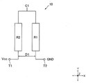
Fig. 3 is a diagram for explaining the structure of the MR sensor 10 shown in fig. 1.
As shown in fig. 3, the MR sensor 10 includes, as an MR element (magnetoresistance effect element), a first resistor R1 (hereinafter referred to as a resistor R1) and a second resistor R2 (hereinafter referred to as a resistor R2) connected in series with each other. The resistors R1 and R2 are formed of a nickel-iron alloy thin film, for example. The resistors R1 and R2 are formed by being folded a plurality of times in the Y direction (the short side direction of the card 2). For example, the resistors R1 and R2 are formed by being folded twice in the Y direction. Alternatively, the resistors R1 and R2 are formed in a straight line parallel to the Y direction. The resistors R1 and R2 may be made of a material other than a nickel-iron alloy.
Resistor R2 is connected to power supply Vcc. Specifically, one end of the resistor R2 not connected to the resistor R1 is connected to a connection terminal T1 connected to the power supply Vcc, and the connection terminal T1 is connected to the power supply Vcc. Resistor R1 is grounded. Specifically, one end of the resistor R1 not connected to the resistor R2 is connected to the ground terminal T2, and the ground terminal T2 is grounded. The potential of the midpoint C1 between the resistor R1 and the resistor R2 connected in series (the connection point between the resistor R1 and the resistor R2) is the output of the MR sensor 10.
The resistance value of the resistor R1 is equal to the resistance value of the resistor R2. In the present embodiment, the length of the resistor R1 in the Y direction is equal to the length of the resistor R2 in the Y direction. The length is narrower than the width of the magnetic data recorded on the magnetic stripe 2a in the Y direction. For example, the length is 2 mm. The width of the resistor R1 in the X direction is equal to the width of the resistor R2 in the X direction. For example, the width is 60 μm. The thickness of the resistor R1 is equal to the thickness of the resistor R2. For example, the film thickness is 45 nm.
The resistor R1 is disposed at the same position as the resistor R2 in the Y direction. Specifically, the resistor R1 and the resistor R2 are disposed at positions in the Y direction where the magnetic stripe 2a passes. The resistor R1 and the resistor R2 are arranged at a distance D1 in the X direction. The distance D1 is a distance smaller than the maximum bit interval of the magnetic data recorded on the magnetic stripe 2 a. That is, the distance D1 is a distance smaller than the bit interval of the magnetic data when the magnetic stripe 2a records "0" data.
In the present embodiment, the distance D1 is half the bit interval of the magnetic data when the magnetic stripe 2a records "0" data. That is, the distance D1 is formed to be the same as the bit interval of the magnetic data when the magnetic stripe 2a records the "1" data. For example, when the recording density of the magnetic data recorded in the magnetic stripe 2a is 75bpi, the distance D1 is 0.17mm (═ 25.4/(75 × 2)), and when the recording density of the magnetic data recorded in the magnetic stripe 2a is 210bpi, the distance D1 is 0.18mm (═ 25.4 × 3/(210 × 2)). When the resistors R1 and R2 are formed by being folded in the Y direction a plurality of times, the distance D1 is the distance between the portion of the resistor R1 closest to the resistor R2 and the portion of the resistor R2 closest to the resistor R1.
(main effect of the present embodiment)
As described above, in the present embodiment, the resistor R1 and the resistor R2 are arranged at the distance D1 in the X direction, and the distance D1 is half the bit interval of the magnetic data when the magnetic stripe 2a records "0" data. That is, in the present embodiment, the distance between the resistor R1 and the resistor R2 in the X direction is very short. Therefore, in the present embodiment, the difference between the amount of resistance change of the resistor R1 and the amount of resistance change of the resistor R2 due to the disturbing magnetic field generated by the disturbing magnetic field generating means 11 can be suppressed to be small. In the present embodiment, the distance D1 in the X direction between the resistor R1 and the resistor R2 is half the bit interval of the magnetic data when the magnetic stripe 2a records "0" data, and therefore the difference between the amount of change in resistance of the resistor R1 and the amount of change in resistance of the resistor R2 due to the "0" data recorded on the magnetic stripe 2a can be increased.
In the present embodiment, the resistance value of the resistor R1 is equal to the resistance value of the resistor R2, and the potential of the midpoint C1 between the resistor R1 and the resistor R2 is the output of the MR sensor 10. In the present embodiment, if it is detected by a card insertion detection mechanism, not shown, that the card 2 has been inserted into the card insertion slot 3, the interference magnetic field generation mechanism 11 generates an interference magnetic field and supplies power to the MR sensor 10. Therefore, in the present embodiment, when magnetic data is recorded in the magnetic stripe 2a of the card 2 inserted into the card insertion port 3, if the card 2 moves to the rear side of the card reader 1, the output signal SG1 of the MR sensor 10 changes as shown in fig. 4.
That is, as shown in fig. 4, the amplitude of output signal SG1 before the recording region of the magnetic data of magnetic stripe 2a reaches MR sensor 10 (before the preamble of magnetic stripe 2a reaches MR sensor 10) is very small, but if the preamble of magnetic stripe 2a reaches MR sensor 10, the amplitude of output signal SG1 becomes large. Therefore, in the present embodiment, even in a state where the disturbing magnetic field is generated, it can be appropriately detected by the MR sensor 10 whether or not the magnetic data is recorded in the magnetic stripe 2a of the card 2 inserted from the card insertion port 3.
(other embodiments)
The above embodiment is an example of a preferred embodiment of the present invention, but the present invention is not limited thereto, and various modifications can be made within a scope not changing the gist of the present invention.
In the above embodiment, the resistor R1 and the resistor R2 are connected in series, but the resistor R1 and the resistor R2 may be connected in parallel. In this case, the difference between the amount of change in resistance of the resistor R1 and the amount of change in resistance of the resistor R2 may be calculated by a predetermined circuit, and whether or not magnetic data is recorded in the magnetic stripe 2a may be detected. However, as in the above-described embodiment, if the resistor R1 is connected in series with the resistor R2, the difference between the amount of change in resistance of the resistor R1 and the amount of change in resistance of the resistor R2 can be directly used as the output of the MR sensor 10, and therefore, the output signal of the MR sensor 10 can be more easily processed than when the resistor R1 and the resistor R2 are connected in parallel.
In the above embodiment, the distance D1 between the resistor R1 and the resistor R2 is half the bit interval of the magnetic data when the magnetic stripe 2a records "0" data. In addition, for example, as long as the distance D1 is a distance smaller than the bit interval of the magnetic data when the magnetic stripe 2a records "0" data, the distance may be a distance other than half of the bit interval of the magnetic data when the magnetic data records "0" data.
In the above embodiment, magnetic data of a plurality of tracks may be recorded on the magnetic stripe 2 a. In this case, the MR sensor 10 has a plurality of sets of first resistive elements and second resistive elements for detecting whether or not magnetic data is recorded on each track. For example, the magnetic data of two tracks, that is, the magnetic data of the first track and the magnetic data of the second track, may be recorded on the magnetic stripe 2 a. In this case, the MR sensor 10 has: a first resistor and a second resistor for detecting whether or not magnetic data is recorded on a first track; and a first resistor and a second resistor for detecting whether or not magnetic data is recorded on the second track. In this case, the first and second resistors for detecting whether or not magnetic data is recorded on the first track are configured similarly to the resistors R1 and R2 of the above-described embodiment, and the first and second resistors for detecting whether or not magnetic data is recorded on the second track are also configured similarly to the resistors R1 and R2 of the above-described embodiment. The distance in the X direction between the first resistor and the second resistor for detecting whether or not magnetic data is recorded on the first track is, for example, half of the bit interval of magnetic data when "0" data is recorded on the first track, and the distance in the X direction between the first resistor and the second resistor for detecting whether or not magnetic data is recorded on the second track is, for example, half of the bit interval of magnetic data when "0" data is recorded on the second track.
In the above embodiment, the card reader 1 is a card-carrying type card reader having the driving roller 8 and the pad roller 9, but the card reader 1 may be a manual type card reader that is manually operated by a user.
Description of the reference numerals
1 card reader
2 card
2a magnetic strip
3 card insertion opening
10 MR sensor
11 disturbing magnetic field generating mechanism
Midpoint of C1
R1 resistor (first resistor)
R2 resistor (second resistor)
X direction of movement of the card.
Claims (5)
1. A card reader, comprising:
a card insertion opening into which a card having a magnetic stripe is inserted;
an MR sensor for detecting whether magnetic data is recorded on the magnetic stripe; and
an interference magnetic field generating mechanism that generates an interference magnetic field for interfering with improper reading of magnetic data recorded in the magnetic stripe,
magnetic data is recorded in the magnetic stripe, the magnetic data being aligned in a moving direction of the card inserted from the card insertion port,
the MR sensor includes a first resistor and a second resistor, and the first resistor and the second resistor are arranged in a state of being separated by a distance smaller than a bit interval of magnetic data when 0 data is recorded on the magnetic stripe in a moving direction of the card.
2. The card reader of claim 1,
the first resistor and the second resistor are arranged apart from each other in the moving direction of the card by a distance corresponding to half of a bit interval of magnetic data when 0 data is recorded in the magnetic stripe.
3. The card reader according to claim 1 or 2,
the first resistor and the second resistor are connected in series,
one of the first resistor and the second resistor is connected to a power supply,
the other of the first resistor and the second resistor is grounded,
the potential of the midpoint between the first resistor and the second resistor is an output of the MR sensor.
4. The card reader according to claim 1 or 2,
the MR sensor has a plurality of sets of the first resistor body and the second resistor body,
the MR sensor detects whether magnetic data is recorded in each of a plurality of magnetic tracks provided to the magnetic stripe.
5. The card reader of claim 3,
the MR sensor has a plurality of sets of the first resistor body and the second resistor body,
the MR sensor detects whether magnetic data is recorded in each of a plurality of magnetic tracks provided to the magnetic stripe.
Applications Claiming Priority (3)
| Application Number | Priority Date | Filing Date | Title |
|---|---|---|---|
| JP2015067983A JP2016189055A (en) | 2015-03-30 | 2015-03-30 | Card reader |
| JP2015-067983 | 2015-03-30 | ||
| PCT/JP2016/060130 WO2016158952A1 (en) | 2015-03-30 | 2016-03-29 | Card reader |
Publications (2)
| Publication Number | Publication Date |
|---|---|
| CN107430674A CN107430674A (en) | 2017-12-01 |
| CN107430674B true CN107430674B (en) | 2020-03-27 |
Family
ID=57005951
Family Applications (1)
| Application Number | Title | Priority Date | Filing Date |
|---|---|---|---|
| CN201680019128.XA Active CN107430674B (en) | 2015-03-30 | 2016-03-29 | Card reader |
Country Status (5)
| Country | Link |
|---|---|
| US (1) | US10055615B2 (en) |
| EP (1) | EP3279828B1 (en) |
| JP (1) | JP2016189055A (en) |
| CN (1) | CN107430674B (en) |
| WO (1) | WO2016158952A1 (en) |
Families Citing this family (4)
| Publication number | Priority date | Publication date | Assignee | Title |
|---|---|---|---|---|
| JP7085814B2 (en) * | 2017-08-31 | 2022-06-17 | 日本電産サンキョー株式会社 | Card reader |
| US10496914B2 (en) * | 2017-10-31 | 2019-12-03 | University Of Florida Research Foundation, Incorporated | Payment card overlay skimmer detection |
| JP2020113357A (en) * | 2019-01-17 | 2020-07-27 | 日本電産サンキョー株式会社 | Magnetic recording medium processor and control method |
| CN112085905B (en) * | 2019-06-14 | 2022-03-01 | 中电金融设备系统(深圳)有限公司 | Magnetic stripe card reader, magnetic stripe data processing device and magnetic stripe data processing method |
Citations (6)
| Publication number | Priority date | Publication date | Assignee | Title |
|---|---|---|---|---|
| CN102341854A (en) * | 2009-03-05 | 2012-02-01 | 日本电产三协株式会社 | Card reader and method of controlling card reader |
| CN103210402A (en) * | 2010-12-22 | 2013-07-17 | 日立欧姆龙金融系统有限公司 | Apparatus for reading magnetic recording medium |
| CN103403740A (en) * | 2011-06-29 | 2013-11-20 | 日本电产三协株式会社 | Card insertion unit and card reader |
| CN103718219A (en) * | 2011-08-30 | 2014-04-09 | 日立欧姆龙金融系统有限公司 | Device for reading magnetic recording medium |
| EP2752825A1 (en) * | 2011-08-30 | 2014-07-09 | Hitachi-Omron Terminal Solutions, Corporation | Device for reading magnetic recording medium |
| CN104471591A (en) * | 2012-07-10 | 2015-03-25 | 日本电产三协株式会社 | Card reader |
Family Cites Families (10)
| Publication number | Priority date | Publication date | Assignee | Title |
|---|---|---|---|---|
| JPS58129585A (en) * | 1982-01-27 | 1983-08-02 | Denki Onkyo Co Ltd | Pattern recognizing device using magnetoresistance element |
| US5266786A (en) * | 1991-10-01 | 1993-11-30 | Ncr Corporation | Magnetoresistive head for reading magnetic ink characters |
| JPH08145718A (en) * | 1994-11-17 | 1996-06-07 | Canon Electron Inc | Magneto-resistive sensor |
| JPH097119A (en) * | 1995-06-19 | 1997-01-10 | Oki Electric Ind Co Ltd | Magnetic head array and its production |
| US5650606A (en) * | 1995-08-07 | 1997-07-22 | Magnetic Products International, Corp | Accurate read/write head for preventing credit card alteration and counterfeiting of debit cards |
| JP3936496B2 (en) * | 1999-08-31 | 2007-06-27 | 日本電産サンキョー株式会社 | Magnetic card transaction device |
| US20080290167A1 (en) * | 2007-05-24 | 2008-11-27 | Clay Von Mueller | Multi dimensional read head array |
| WO2013118183A1 (en) * | 2012-02-09 | 2013-08-15 | 日立オムロンターミナルソリューションズ株式会社 | Magnetic card reader and magnetic card reading method |
| JP6039070B2 (en) * | 2013-06-04 | 2016-12-07 | 日立オムロンターミナルソリューションズ株式会社 | Magnetic recording medium reader |
| DE102014119663A1 (en) * | 2014-12-29 | 2016-06-30 | Infineon Technologies Ag | smart card |
-
2015
- 2015-03-30 JP JP2015067983A patent/JP2016189055A/en active Pending
-
2016
- 2016-03-29 EP EP16772833.6A patent/EP3279828B1/en active Active
- 2016-03-29 CN CN201680019128.XA patent/CN107430674B/en active Active
- 2016-03-29 WO PCT/JP2016/060130 patent/WO2016158952A1/en active Application Filing
- 2016-03-29 US US15/563,091 patent/US10055615B2/en active Active
Patent Citations (6)
| Publication number | Priority date | Publication date | Assignee | Title |
|---|---|---|---|---|
| CN102341854A (en) * | 2009-03-05 | 2012-02-01 | 日本电产三协株式会社 | Card reader and method of controlling card reader |
| CN103210402A (en) * | 2010-12-22 | 2013-07-17 | 日立欧姆龙金融系统有限公司 | Apparatus for reading magnetic recording medium |
| CN103403740A (en) * | 2011-06-29 | 2013-11-20 | 日本电产三协株式会社 | Card insertion unit and card reader |
| CN103718219A (en) * | 2011-08-30 | 2014-04-09 | 日立欧姆龙金融系统有限公司 | Device for reading magnetic recording medium |
| EP2752825A1 (en) * | 2011-08-30 | 2014-07-09 | Hitachi-Omron Terminal Solutions, Corporation | Device for reading magnetic recording medium |
| CN104471591A (en) * | 2012-07-10 | 2015-03-25 | 日本电产三协株式会社 | Card reader |
Also Published As
| Publication number | Publication date |
|---|---|
| EP3279828A4 (en) | 2018-11-07 |
| US20180075263A1 (en) | 2018-03-15 |
| EP3279828B1 (en) | 2019-10-30 |
| JP2016189055A (en) | 2016-11-04 |
| US10055615B2 (en) | 2018-08-21 |
| WO2016158952A1 (en) | 2016-10-06 |
| CN107430674A (en) | 2017-12-01 |
| EP3279828A1 (en) | 2018-02-07 |
Similar Documents
| Publication | Publication Date | Title |
|---|---|---|
| US8985450B2 (en) | Card insertion part and card reader | |
| CN107430674B (en) | Card reader | |
| US9734363B2 (en) | Card reader | |
| US7364092B2 (en) | Electronic stripe cards | |
| JP6461670B2 (en) | Card reader and card reader control method | |
| JP2011070746A (en) | Card reader, and method of controlling card reader | |
| JP4075754B2 (en) | Non-contact communication medium insertion slot module | |
| EP3168773A1 (en) | Card reader | |
| US20170185811A1 (en) | Card reader and control method for card reader | |
| US10902225B2 (en) | Card reader | |
| JP6125439B2 (en) | Card reader | |
| US9858449B2 (en) | MR sensor and card reader | |
| KR101555772B1 (en) | Method for determining coercivity of magnetic recording medium | |
| JP7085932B2 (en) | Card reader | |
| JP2008293377A (en) | Magnetic recorder | |
| JP2019149215A (en) | Card reader | |
| JP2004070538A (en) | Card reader | |
| JP2019102107A (en) | Card reader and control method for card reader | |
| JP3663314B2 (en) | Recording medium detection apparatus and recording medium detection method | |
| JP2019100730A (en) | Card reader and control method for card reader | |
| JP2019061398A (en) | Magnetic sensor unit and card reader | |
| KR20130097321A (en) | Combined bankbook printer | |
| JP2006260674A (en) | Magnetic recording data reader |
Legal Events
| Date | Code | Title | Description |
|---|---|---|---|
| PB01 | Publication | ||
| PB01 | Publication | ||
| SE01 | Entry into force of request for substantive examination | ||
| GR01 | Patent grant | ||
| GR01 | Patent grant |