CN107302350B - Method and apparatus for tuning a voltage - Google Patents
Method and apparatus for tuning a voltage Download PDFInfo
- Publication number
- CN107302350B CN107302350B CN201710515078.0A CN201710515078A CN107302350B CN 107302350 B CN107302350 B CN 107302350B CN 201710515078 A CN201710515078 A CN 201710515078A CN 107302350 B CN107302350 B CN 107302350B
- Authority
- CN
- China
- Prior art keywords
- voltage
- flip
- flop
- clock
- clock signal
- Prior art date
- Legal status (The legal status is an assumption and is not a legal conclusion. Google has not performed a legal analysis and makes no representation as to the accuracy of the status listed.)
- Active
Links
Images


Classifications
-
- H—ELECTRICITY
- H03—ELECTRONIC CIRCUITRY
- H03K—PULSE TECHNIQUE
- H03K3/00—Circuits for generating electric pulses; Monostable, bistable or multistable circuits
- H03K3/01—Details
- H03K3/012—Modifications of generator to improve response time or to decrease power consumption
-
- H—ELECTRICITY
- H03—ELECTRONIC CIRCUITRY
- H03K—PULSE TECHNIQUE
- H03K3/00—Circuits for generating electric pulses; Monostable, bistable or multistable circuits
- H03K3/02—Generators characterised by the type of circuit or by the means used for producing pulses
- H03K3/027—Generators characterised by the type of circuit or by the means used for producing pulses by the use of logic circuits, with internal or external positive feedback
- H03K3/037—Bistable circuits
- H03K3/0375—Bistable circuits provided with means for increasing reliability; for protection; for ensuring a predetermined initial state when the supply voltage has been applied; for storing the actual state when the supply voltage fails
-
- H—ELECTRICITY
- H03—ELECTRONIC CIRCUITRY
- H03K—PULSE TECHNIQUE
- H03K3/00—Circuits for generating electric pulses; Monostable, bistable or multistable circuits
- H03K3/02—Generators characterised by the type of circuit or by the means used for producing pulses
- H03K3/353—Generators characterised by the type of circuit or by the means used for producing pulses by the use, as active elements, of field-effect transistors with internal or external positive feedback
- H03K3/356—Bistable circuits
- H03K3/356104—Bistable circuits using complementary field-effect transistors
-
- H—ELECTRICITY
- H03—ELECTRONIC CIRCUITRY
- H03K—PULSE TECHNIQUE
- H03K3/00—Circuits for generating electric pulses; Monostable, bistable or multistable circuits
- H03K3/02—Generators characterised by the type of circuit or by the means used for producing pulses
- H03K3/353—Generators characterised by the type of circuit or by the means used for producing pulses by the use, as active elements, of field-effect transistors with internal or external positive feedback
- H03K3/356—Bistable circuits
Landscapes
- Logic Circuits (AREA)
- Manipulation Of Pulses (AREA)
- Semiconductor Integrated Circuits (AREA)
Abstract
Systems and methods for operating transistors near or in a sub-threshold region to reduce power consumption are described herein. In one embodiment, a method for low power operation includes sending a clock signal (Ck) to a flip-flop (150) via a clock path (225) including a plurality of transistors, wherein the clock signal has a high state corresponding to a high Voltage (VH) that is higher than a threshold voltage of the transistors in the clock path (225). The method also includes sending a data signal (D) to the flip-flop (150) via a data path (135) including a plurality of transistors, wherein the data signal has a high state corresponding to a low Voltage (VL) that is lower than a threshold voltage of the transistors in the data path (135). The method also includes latching the data signal (D) at the flip-flop (150) using the clock signal (Ck).
Description
The application is a divisional application of a Chinese patent application with the application number of 201480013290.1, 3-14-2014, entitled "low power architecture".
RELATED APPLICATIONS
This application claims priority from U.S. provisional application No.61/800,116 filed 3/15/2013, in accordance with 35u.s.c. § 119(e), the entire specification of which is incorporated herein by reference.
Background
FIELD
Aspects of the present disclosure relate generally to low power devices, and more particularly to low power devices in which transistors operate near or in sub-threshold regions to reduce power consumption.
Background
Transistors in the device may be operated near or in the sub-threshold region to significantly reduce the power consumption of the device. For example, subthreshold operation minimizes energy consumption per cycle.
SUMMARY
The following presents a simplified summary of one or more embodiments in order to provide a basic understanding of such embodiments. This summary is not an extensive overview of all contemplated embodiments, and is intended to neither identify key or critical elements of all embodiments nor delineate the scope of any or all embodiments. Its sole purpose is to present some concepts of one or more embodiments in a simplified form as a prelude to the more detailed description that is presented later.
According to an aspect, a low power device is described herein. The low power device includes: a clock path for propagating a clock signal, wherein the clock path comprises a plurality of transistors; and a clock source configured to generate a clock signal having a high state corresponding to a high voltage above a threshold voltage of the transistors in the clock path. The low power device further comprises: a data path for propagating a data signal, wherein the data path includes a plurality of transistors; and a data source configured to generate a data signal having a high state corresponding to a low voltage that is lower than a threshold voltage of a transistor in the data path. The apparatus also includes a flip-flop configured to receive the clock signal from the clock path, receive the data signal from the data path, and latch the data signal using the clock signal.
A second aspect relates to a method for low power operation. The method includes sending a clock signal to a flip-flop via a clock path including a plurality of transistors, wherein the clock signal has a high state corresponding to a high voltage that is higher than a threshold voltage of the transistors in the clock path. The method also includes sending a data signal to the flip-flop via a data path including a plurality of transistors, wherein the data signal has a high state corresponding to a low voltage that is lower than a threshold voltage of a transistor in the data path. The method also includes latching the data signal at the flip-flop using the clock signal.
A third aspect relates to an apparatus for tuning a voltage. The apparatus comprises: a data path for propagating a data signal; a first flip-flop configured to receive a data signal from the data path, receive a clock signal, and latch the data signal using the clock signal; and a second flip-flop configured to receive the data signal from the data path, receive a delayed version of the clock signal, and latch the data signal using the delayed version of the clock signal. The apparatus further comprises: a circuit configured to detect a mismatch between the outputs of the first and second flip-flops; and a voltage regulator that adjusts the voltage based on the detected mismatch.
A fourth aspect relates to a method for tuning a voltage. The method comprises the following steps: transmitting a data signal to the first and second flip-flops via the data path; latching a data signal using a clock signal at a first flip-flop; and latching the data signal at the second flip-flop using the delayed version of the clock signal. The method further comprises the following steps: detecting a mismatch between the outputs of the first and second flip-flops; and adjusting the voltage based on the detected mismatch.
To the accomplishment of the foregoing and related ends, the one or more embodiments comprise the features hereinafter fully described and particularly pointed out in the claims. The following description and the annexed drawings set forth in detail certain illustrative aspects of the one or more embodiments. These aspects are indicative, however, of but a few of the various ways in which the principles of various embodiments may be employed and the described embodiments are intended to include all such aspects and their equivalents.
Brief Description of Drawings
Fig. 1A illustrates a high voltage clock signal according to an embodiment of the present disclosure.
Fig. 1B illustrates a clock tree according to an embodiment of the present disclosure.
Fig. 2A illustrates a high voltage clock signal according to another embodiment of the present disclosure.
Fig. 2B illustrates a clock tree according to another embodiment of the present disclosure.
Fig. 3 shows an example of a CMOS transmission gate.
Fig. 4 shows an example of a single NFET pass gate.
Fig. 5 shows an example of a flip-flop with CMOS transmission gates.
Fig. 6 shows an example of a flip-flop with a single NFET pass gate.
Fig. 7 illustrates an example of a clock tree with a voltage converter at the end of the clock tree according to an embodiment of the present disclosure.
Fig. 8A shows an example of a clock signal input to a converter according to an embodiment of the present disclosure.
Fig. 8B illustrates an example of a converted clock signal output from a conversion according to an embodiment of the present disclosure.
Fig. 9 illustrates an exemplary implementation of a converter according to an embodiment of the disclosure.
Fig. 10 shows an example of a Low Dropout (LDO) regulator.
Fig. 11 illustrates a switched capacitor DC-DC converter according to an embodiment of the disclosure.
Figure 12 illustrates a tuning circuit for adjusting a low power supply voltage according to an embodiment of the present disclosure.
Fig. 13 shows an exemplary implementation of an inverter.
Fig. 14 shows another exemplary implementation of an inverter.
Fig. 15 is a flow diagram illustrating a method 1500 for low power operation according to an embodiment of the disclosure.
Fig. 16 is a flow diagram illustrating a method 1600 for tuning a voltage according to an embodiment of the present disclosure.
Detailed Description
The detailed description set forth below in connection with the appended drawings is intended as a description of various configurations and is not intended to represent the only configurations in which the concepts described herein may be practiced. The detailed description includes specific details in order to provide a thorough understanding of the various concepts. It will be apparent, however, to one skilled in the art that these concepts may be practiced without these specific details. In some instances, well-known structures and components are shown in block diagram form in order to avoid obscuring such concepts.
In a system, a clock signal may be generated at a clock source and distributed to different devices (e.g., flip-flops) in the system via a clock tree. The clock tree may branch to multiple clock paths for distributing the clock signal to different devices. The clock tree may include one or more buffers (e.g., inverters) along each clock path.
A data signal may originate from a data source in the system and propagate down a data path to devices (e.g., flip-flops) in the system. The system may include one or more buffers (e.g., inverters) and/or other types of logic along the data path. For the example of a flip-flop, the flip-flop may receive a data signal from the data path and a clock signal from the clock tree. The flip-flop may use a clock signal to time the latching of the data signal at the flip-flop. For example, the flip-flop may latch the logic value of the data signal at each rising or falling edge of the clock signal. In order for the flip-flop to properly latch the logic value of the data signal, the logic value should stabilize (not change) for a period of time (called the dwell time) after the rising or falling edge of the clock. Failure to meet this timing condition results in a retention violation that may cause the flip-flop to enter a meta-stable state. In conventional systems, the propagation delays in the clock tree and data path are adjusted (e.g., using buffers) to ensure that this timing condition is met.
However, controlling the timing of data and clock propagation delays is very difficult for systems in which the transistor is intentionally operated in the subthreshold region (i.e., systems in which the maximum gate voltage provided to the transistor intended to turn on the transistor is less than the threshold voltage of the transistor). This is because the current of a transistor is exponentially related to the gate voltage when the transistor is operating in the sub-threshold region, thereby making the current of the transistor exponentially sensitive to the threshold voltage (Vt) and/or the supply voltage of the transistor. Thus, even very small variations in threshold voltage and/or supply voltage between transistors operating in the sub-threshold region may result in large variations in their currents. This in turn leads to large variations in delay between buffers and/or other logic implemented with transistors and thus to large variations in propagation delay in clock trees and data paths. The large variation in propagation delay makes it very difficult to control the timing of the clock signal relative to the data signal at the flip-flop to meet the set-aside condition. For example, two paths with the same number of buffers may have very different delays due to Vt and/or supply voltage variations.
Embodiments of the present disclosure use a high voltage clock signal to address the above issues while still using a low voltage data signal to reduce power consumption (e.g., the data signal has a high state corresponding to a sub-threshold voltage). In this regard, FIG. 1A illustrates a voltage-time diagram of a high voltage clock signal 110 according to one embodiment. The voltage of the high voltage clock signal 110 may swing between a high Voltage (VH) and ground, where VH may be greater than the threshold voltage of the transistors in the clock tree. For example, VH may be several hundred millivolts above the threshold voltage and may be the voltage of a battery used to power the portable device in which the high voltage clock signal 110 is used.
Fig. 1B shows an example of a corresponding clock source 120 and clock tree 125. Clock source 120 generates a high voltage clock signal 110 that is distributed to devices via clock tree 125. The clock tree 125 may include buffers powered by VH, which may be higher than the threshold voltage of the transistors in the buffers. When VH is higher than the threshold voltage of the transistors in the clock tree 125, these transistors operate in the strong inversion region and are therefore much faster than transistors operating in the subthreshold region. As a result, the propagation delay of the high voltage clock signal 110 is much shorter than the propagation delay of the data signal, as discussed further below.
FIG. 1B also shows an example of a data source 130 and a data path 135. The data source 130 initiates a data signal. The voltage of the data signal may have a swing between a low Voltage (VL) and ground, where VL is about or below the threshold voltage of the transistors in the data path 135. For example, VL may be about 300 mV. Fig. 1A shows an example of VL versus VH. The data path 135 may include a plurality of buffers, computational logic, and/or other types of logic devices that are powered by the VL. This causes the transistors in the data path 135 to operate in the subthreshold region and thus much slower than the transistors in the clock tree 125 (which may operate in the strong inversion region). As a result, the propagation delay of the high voltage clock signal is much shorter than the propagation delay of the data signal.
Because the transistors in the data path 135 operate in the sub-threshold region, the propagation delay of the data signal can vary over a wide range, depending on the threshold voltage of the transistors and/or other factors. However, the propagation delay of the high voltage clock signal is much shorter than even the shortest propagation delay in this range. Thus, when the high voltage clock signal and the data signal are input to the flip-flop 150 (an example of which is shown in fig. 1B), the high voltage clock signal is actually guaranteed to propagate to the flip-flop 150 at least a set time ahead of the data signal. Thus, the high voltage clock signal prevents a retention violation.
Fig. 2A shows a voltage-time diagram of a high voltage clock signal 210 according to another embodiment. The voltage of the high voltage clock signal 210 may swing between VH and VL. As discussed further below, this allows charge from the clock tree to be dumped into the low power supply used to power logic operating in the subthreshold region. The voltage difference VH-VL may be at or above the threshold voltage of the transistors in the clock tree. Fig. 2A also shows an example of a data signal 212 having a voltage swing between VL and ground, where VL may correspond to a logic 1 and ground may correspond to a logic 0. It will be appreciated that the relative positions of the data edges and clock edges shown in fig. 2A are merely exemplary and may vary (e.g., depending on the relative propagation delays).
Fig. 2B shows an example of a corresponding clock source 220 and clock tree 225. Clock source 220 generates a high voltage clock signal 210 that is distributed to devices via a clock tree 225. The clock tree 125 may include buffers that are powered between VH and VL, as shown in fig. 2B. Because the voltage difference VH-VL is at or above the threshold voltage of the transistors in the clock tree 225, these transistors are much faster than transistors operating in the subthreshold region. As a result, the propagation delay of the high voltage clock signal 210 is much shorter than the propagation delay of the data signal in the data path 135, thereby preventing a retention violation.
The clock frequency of the high voltage clock signal 110/210 may also be adjusted to prevent setup violations. A setup violation may occur when the data signal does not propagate to the flip-flop fast enough for the data signal to settle to a stable value at the flip-flop before the flip-flop admits (clock in) the clock edge of the data signal. When this occurs, the clock frequency may be slowed down to provide more time for the data signal to settle before the clock edge. The clock edge transitions very fast compared to the data because the clock edge transition slope is determined by VH instead of VL.
Using VL to operate data and/or logic significantly reduces power consumption compared to VH. This significantly extends the battery life of very low power devices, such as battery powered medical devices, tracking devices, and "always on" devices that can be on for extended periods of time (e.g., years) but are powered by batteries because of the low power consumption of the device.
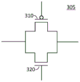
The high voltage clock signal 110/210 may be used to reduce the gate count (number of transistors) in the flip-flop by replacing at least one CMOS pass gate in the flip-flop with a single NFET. In this regard, fig. 3 shows an example of a CMOS transmission gate 305 that is typically used in a flip-flop to transmit the logic value of a data signal within the flip-flop. The CMOS pass gate includes a PFET 310 and an NFET 320 coupled in parallel. The gates of PFET 310 and NFET 320 are driven by complementary signals. For example, the gate of NFET 320 may be driven by a clock signal and the gate of PFET 310 may be driven by the inverse of the clock signal, or vice versa. PFET 310 is used to transmit a high logic value and NFET 320 is used to transmit a low logic value.
FIG. 4 shows an example of a pass gate 405 including a single NFET 420 without a PFET. When the high state of the clock signal driving the gate of NFET 420 corresponds to a voltage that is about the same as the high logic value, a single NFET 420 may not be able to transmit the high logic value. This is because the voltage at the gate of the NFET 420 reduces the gate-to-source voltage of the NFET 420 (e.g., about Vt when the NFET 420 is turned on) at the output 440 of the pass gate 420. If the high logic value corresponds to a voltage below Vt, the voltage at output 440 may drop to zero.
The high voltage clock signal 110/210 according to embodiments of the present disclosure allows a single NFET 420 to transmit a high logic value. This is because the high state of the high voltage clock signal 110/210 corresponds to a Voltage (VH) that is higher than the high logic Value (VL) of the data signal. As a result, even when the voltage at the gate (VH) of NFET 420 decreases the gate-to-source voltage of NFET 420 at output 440, the voltage at output 440 can still be about VL. This assumes that the voltage difference VH-VL is large enough (e.g., at least as large as the threshold voltage Vt of NFET 420) to sink the gate-to-source voltage of NFET 420 when NFET 420 is turned on.
In this regard, fig. 5 and 6 illustrate an example of gate count reduction using a high voltage clock signal 110/210 according to various embodiments of the present disclosure. Fig. 5 shows an example of a flip-flop 505 comprising a CMOS transmission gate 510, a tri-state inverter 520, and an inverter 530. The tristate inverter 520 and inverter 530 form a switchable latch and the CMOS transmission gate 510 is used to transmit a logical data value to the latch.
Fig. 6 shows an example of a flip-flop 605 in which the CMOS pass gate 510 is replaced by a first single NFET pass gate 610 and the tristate inverter 520 is replaced by a second single NFET pass gate 620 and an inverter 630. This reduces the gate count of flip-flop 605 by at least two compared to flip-flop 505 of fig. 5. Back-to- back inverters 630 and 640 form a latch that is switched by second single NFET pass gate 620. In this example, the data signal may have a voltage swing between VL and ground to reduce power consumption, as discussed above. One or more of the inverters in flip-flop 605 may be powered by VL to operate the corresponding transistor in the subthreshold region to save power. The single NFET pass gates 610 and 620 are clocked by a high voltage clock signal or its inverse. As discussed above, the high voltage clock signal enables the use of single NFET pass gates to reduce gate counts.
The gate count in the scan multiplexer may also be reduced. Conventional scan multiplexers include PFETs and NFETs for switching the multiplexer between a scan path to test the functionality of one or more flip-flops and a data path for normal operation. Because the data operates at VL, the gate count of the multiplexer can be reduced by replacing the PFET and NFET pairs in the multiplexer with a single NFET and coupling the gate of the single NFET to either VH or ground (depending on whether the single NFET is turned on or off). In normal operation, a single NFET is either always on or always off, because in normal operation the multiplexer is always switched to the data path. Thus, a single NFET does not consume the dynamic power associated with a flip NFET, and the gate of the NFET may be hardwired to VH or ground.
As discussed above (e.g., with respect to fig. 2A and 2B), the voltage of the high voltage clock signal 210 swings between VH and VL. Thus, the high voltage clock signal 210 has a low state corresponding to the voltage of VL. In some applications VL may not be low enough to completely turn off the transmission gate, resulting in that leakage current may be too high. Thus, in one embodiment, the voltage converter may be placed at the end of the clock tree before the high voltage clock signal 210 is input to the corresponding device (e.g., flip-flop). Fig. 7 shows an example of a voltage converter 710 at the end of the clock tree 225 corresponding to the flip-flop 150. The converter 710 converts the high voltage clock signal 210 into a converted high voltage clock signal having a lower low state voltage. Fig. 8A shows an example of a high voltage clock signal 210 having a voltage swing between VH and VL. Fig. 8B shows the converted high voltage clock signal 810 output from the voltage converter 810. The converted high-voltage clock signal 810 may be slightly delayed compared to the high-voltage clock signal 210 due to internal delays in the converter 710. In this example, the converted high voltage clock signal 810 has a voltage swing (full voltage swing) between VH and ground. The converted high voltage clock signal 810 is input to the flip-flop 150 such that logic in the flip-flop is clocked using the converted clock signal. For example, the converted clock signal 810 may be used to clock a transmission gate, where the lower low state voltage of the converted clock signal 810 reduces leakage current of the transmission gate in the off state.
Fig. 9 illustrates an exemplary implementation of a voltage converter 910 according to an embodiment of the present disclosure. Voltage converter 910 may be used to implement converter 710 shown in fig. 7 to provide a converted clock signal having a full voltage swing. Converter 910 includes a first inverter 915, a second inverter 920, a first PFET 925, a second PFET 930, and a first NFET 935 and a second NFET 940. First and second inverters 915 and 920 are coupled in series and are powered between VH and VL. The sources of the first PFET 925 and the second PFET 930 are coupled to VH, the drain of the first NFET 935 is coupled to the drain of the first PFET 925, the drain of the second NFET 940 is coupled to the drain of the second PFET 930, and the sources of the first NFET 935 and the second NFET 940 are coupled to ground. The gate of the first PFET 925 is driven by the output of the second inverter 920 and the gate of the second PFET 930 is driven by the output of the first inverter 915. The gate of first NFET 935 is cross-coupled to the drains of second PFET 930 and second NFET 940. The gate of second NFET 940 is cross-coupled to the drains of first PFET 925 and first NFET 935. The output of transistor 950 is taken from node 945.
The high voltage clock signal 210 may be input to the first inverter 915. When the input clock signal is in a high state, the gate of first PFET 925 is driven high with voltage VH and the gate of second PFET 930 is driven low with voltage VL. This turns off the first PFET 925 and turns on the second PFET 930 (assuming VH-VL is sufficient to turn on the second PFET 930). This causes the second PFET 930 to pull up the voltage at node 945 to approximately VH.
When the input clock signal is in a low state, the gate of first PFET 925 is driven low with voltage VL and the gate of second PFET 930 is driven high with voltage VH. This turns on the first PFET 925 and turns off the second PFET 930. As a result, first PFET 925 pulls up the voltage at the drain of first PFET 925 to about VH. This voltage is coupled to the gate of second NFET 940, which turns on second NFET 940. This causes the second NFET 940 to pull the voltage at node 945 down to about ground.
Thus, the converted clock signal at the output of converter 910 has about a full voltage swing (between VH and ground). An additional inverter may be added to the output of the converter 910 to invert the converted clock signal. The additional inverter may be powered between VH and ground. It will be appreciated that the circuit shown in fig. 9 is merely exemplary, and that the converter may be implemented using other circuit designs.
The low voltage VL may be provided by a Low Dropout (LDO) regulator. Fig. 10 shows an example of an LDO including an amplifier 1010 and a FET 1020 (e.g., PFET). The reference voltage Vref and the voltage at node 1025 are input to amplifier 1010. Using negative feedback, amplifier 1010 drives the gate of FET 1020 in a direction that minimizes the difference between Vref and the voltage at node 1025, and thereby adjusts the voltage at node 1025 to about Vref. Vref may be set to provide a desired low voltage VL (e.g., using a bandgap reference) to operate logic in the sub-threshold region. Although LDOs may be suitable for providing a stable VL, LDOs may be inefficient. This is because the current to the load 1030 of the logic must pass through the FET 1020. This causes an IR drop across the power dissipating FET 1020 and thus wastes energy.
Thus, in some embodiments, the low voltage VL is provided by a switched capacitor DC-DC converter. Fig. 11 shows a DC-DC converter 1105 according to an embodiment of the disclosure. The converter 1105 includes a first switch 1110, a second switch 1120, a third switch 1125, a fourth switch 1130, and a capacitor C. Capacitor C may include capacitance from the clock tree. For example, the capacitor C may comprise one or more capacitors in a clock tree. This allows the charge for propagating the clock signal in the clock tree to be dumped into the low power supply to operate the logic at VL, providing improved power efficiency.
In fig. 11, phase Φ 1 may correspond to a high state of the clock signal and phase Φ 2 may correspond to a low state of the clock signal. In phase Φ 1, the first and fourth switches 1110 and 1130 are closed and the second and third switches 1120 and 1125 are open. As a result, capacitor C is coupled to VH, and the top of capacitor C is charged to VH. The voltage across capacitor C is charged to about VH-VL.
In phase Φ 2, the first and fourth switches 1110 and 1130 are open and the second and third switches 1120 and 1125 are closed. As a result, capacitor C is coupled between the low power supply and ground. Let VH-VL > VL, which causes charge from capacitor C to be dumped into the storage capacitor CS of the low power supply. This charge provides energy to the load 1140 of the logic operating at VL. Load 1140 may comprise a load (e.g., a buffer) of logic in the data path and/or a load (e.g., an inverter) of logic in a flip-flop operating at VL.
Thus, the voltage at the top end of the capacitor C in the DC-DC converter 1105 switches between about VH and VL. This allows the capacitor C to comprise a capacitor from the clock tree, as the capacitors in the clock tree are also switched between VH and VL to operate the high voltage clock signal 210. Thus, the charge used to propagate the clock in the clock tree can be reused to charge the low voltage power supply. The capacitor in the clock tree may include the capacitance of the output node of each inverter of the clock tree, where each inverter is used as a buffer. Each inverter may charge and discharge a respective output node between VH and VL to propagate a clock signal. When the output node is discharged to VL, charge may be dumped into the low power supply.
In some embodiments, the capacitance from the clock tree may be effectively in parallel with capacitor C. For a true signal of the clock, the PFET drivers in the clock tree may act like switch 1110 on phase Φ 1, and the NFET drivers in the clock tree may act like switch 1120 on phase Φ 2. For glitches of the clock, the switches may effectively operate on opposite phases. The capacitance of the clock tree may share the same top connection as capacitor C, but the bottom plate of the clock tree capacitance may be distributed between VL, ground, and other signals.
In the above example, each inverter in the clock tree may be implemented using a PFET and an NFET (an example of which is shown in fig. 13), where each inverter turns on the respective PFET to charge the respective clock tree capacitance and turns on the respective NFET to discharge the respective clock tree capacitance. Some or all of the PFET drivers discussed in the above examples may correspond to PFETs of inverters, and some or all of the NFET drivers discussed in the above examples may correspond to NFETs of inverters. Thus, a PFET of an inverter may act as a switch charging a respective capacitance (e.g., to VH), and an NFET of the inverter may act as a switch discharging a respective capacitance (e.g., to VL).
The capacitance of the capacitor C may be adjusted so that the amount of charge discharged to the storage capacitor CS of the low power supply per clock cycle approximately complements the amount of charge consumed by the load 1140 per clock cycle. To this end, the capacitor C may comprise a variable capacitor (not shown) coupled in parallel with the capacitor from the clock tree. The capacitance of the variable capacitor may be adjusted so that the amount of charge discharged to the storage capacitor CS of the low power supply per clock cycle approximately supplements the amount of charge consumed by the load 1140 per clock cycle to maintain the desired low voltage. If the capacitance of the clock tree cannot provide sufficient charge to the low power supply, one or more additional capacitors may be added to capacitor C. It will be appreciated that the DC-DC converter shown in fig. 11 is merely exemplary, and that the DC-DC converter may be implemented using other configurations.
Operating the data path/logic at the sub-threshold voltage saves a significant amount of power compared to operating above the threshold voltage. However, as discussed above, the clock is unreliable. Embodiments of the present disclosure use a high voltage clock in conjunction with subthreshold data paths/logic to address timing issues as discussed above. However, running the clock at high voltage consumes more power. Some of the additional power consumed by the high voltage clock is recovered and used to provide the sub-threshold voltage to the data path/logic as illustrated in fig. 11 and discussed above. The result is a very power efficient solution without the timing problems discussed above.
Power consumption can be reduced by reducing the low power supply voltage VL. However, if VL is reduced too much, the system stops working properly. For example, in order for a flip-flop to properly latch the logic value of a data signal, the data signal needs to settle for a period of time before the clock edge (referred to as the setup time) used by the flip-flop to admit (clock in) the data signal. However, as VL decreases, the propagation delay in the corresponding data path increases. This is because the speed of logic (e.g., buffers) in the data path slows down as VL decreases. Eventually, the propagation delay increases to the point where the data signal cannot settle to a stable value in time at the flip-flop to meet the setup time condition. As a result, a setup violation occurs and the flip-flop may enter a meta-stable state. Thus, power consumption can be minimized by reducing the low power supply voltage VL to the minimum voltage required for the system to function properly (the lowest operating voltage).
Figure 12 illustrates a tuning circuit 1205 for tuning the low power supply voltage VL to a voltage near or at the minimum voltage required by the system to prevent setup violations at a given clock frequency, according to one embodiment. Tuning circuit 1205 includes a first test unit 1208-1. Test unit 1208-1 includes normal flip-flop 1210, test flip-flop 1220, and exclusive-or (XOR) gate 1250. The normal flip-flop 1210 is a flip-flop used to latch a data signal in the system and output the latched data to a calculation logic in the system. Test flip-flop 1220 (shadow flip-flop) may be used to approximate the minimum VL required for normal flip-flop 1210 to prevent setup violations, as discussed further below. The test flip-flop 1220 and the normal flip-flop 1210 may be implemented using the same circuitry such that the test flip-flop 1220 mimics the normal flip-flop 1210.
The test flip-flop 1220 and the normal flip-flop 1210 are coupled to the end of the same data path 1235. As a result, the timing of the data signals at the test flip-flop 1220 and the normal flip-flop 1210 are approximately the same. The clock inputs of the test flip-flop 1220 and the normal flip-flop 1210 are coupled to different points along the clock path 1225, where the clock signal on the clock path 1225 must propagate through the delay element 1227 before reaching the normal flip-flop 1210, as compared to the test flip-flop 1220. As a result, the test flip-flop 1220 receives an earlier version of the clock signal received by the normal flip-flop 1210. The earlier version of the clock signal advances by an amount approximately equal to the time delay of delay element 1227.
The output of normal flip-flop 1210 is coupled to a first input of exclusive-or gate 1250, and the output of test flip-flop 1220 is coupled to a second input of exclusive-or gate 1250. The output of normal flip-flop 1210 is also coupled to computational logic. When the outputs of the normal flip-flop 1210 and the test flip-flop 1220 match, the exclusive or gate 1250 outputs a logic 0. This may indicate that both flip- flops 1210 and 1220 are functioning properly. When the outputs of the normal flip-flop 1210 and the test flip-flop 1220 do not match, the exclusive or gate 1250 outputs a logic 0. This may indicate that a setup violation has occurred at test trigger 1220, as discussed further below.
To determine the minimum VL at which normal flip-flop 1210 is operating properly, the output of xor gate 1250 may be monitored as VL decreases. Initially, the output of exclusive or gate 1250 may be a logic 0, indicating that both flip- flops 1210 and 1220 are functioning properly. As VL decreases, the propagation delay of data path 1235 increases. At some point, a setup violation will begin to occur at test flip-flop 1220 but not at normal flip-flop 1210. This is because the test flip-flop 1220 clocks the data signal using an earlier version of the clock signal used by the normal flip-flop 1210. Thus, while the test flip-flop 1220 may begin to experience setup violations, the normal flip-flop 1210 may still function correctly. However, this may indicate that if VL is lowered again, then normal trigger 1210 will also start experiencing setup violations. Thus, the voltage at which the test flip-flop 1220 begins to experience a setup violation may be used as an approximation of the minimum low power supply voltage VL required by the normal flip-flop 1210 to prevent setup violations.
When the test flip-flop 1220 begins to experience a setup violation, the outputs of the test flip-flop 1220 and the normal flip-flop 1210 stop matching and the exclusive-or gate 1250 outputs a logic 1. Thus, the voltage at which xor gate 1250 begins to output a logic 1 may be used as an approximation of the minimum low power supply voltage VL required for normal flip-flop 1210 to prevent setup violations.
As shown in FIG. 12, the tuning circuit 1205 may include a plurality of test cells 1208-1 through 1208-N, where each test cell includes a test flip-flop that is paired with a normal flip-flop in the system and an XOR gate coupled to the outputs of the respective test flip-flop and normal flip-flop. Each of the test units 1208-1 through 1208-N may be implemented using the circuitry shown in FIG. 12 for test unit 1208-1. For ease of illustration, only the exclusive OR gates of test cells 1208-2 and 1208-N are shown in FIG. 12. In operation, each test cell 1208-1 through 1208-N may output a 0 when the outputs of the corresponding test flip-flop and the normal flip-flop match and a 1 when the outputs of the corresponding test flip-flop and the normal flip-flop do not match.
The test units 1208-1 and 1208-N may be distributed across the chip to test different areas of the chip, which may experience different propagation delays due to process-voltage-temperature (PVT) variations across the chip. Test units 1208-1 and 1208-N may have different data paths and/or different numbers of clock buffers.
The tuning circuit 1205 may also include an encoder 1260 and a voltage regulator 1270. The outputs of test units 1208-1 through 1208-N are coupled to encoder 1260. The encoder 1260 may be configured to count the number of test units 1208-1 through 1208-N that output logic 1 and output the count value to the voltage regulator 1270. The voltage regulator 1270 may use the count value to determine the minimum low power supply voltage VL. For example, the voltage regulator 1270 may gradually decrease VL while monitoring the count value. The voltage regulator 1270 may stop decreasing VL when the count value reaches a threshold value. The voltage regulator 1270 may then continue to monitor the count value. If the count value rises above the threshold (e.g., for a certain period of time), the voltage regulator 1270 may increase VL until the count value falls back to the threshold. In this context, the threshold corresponds to some error rate (e.g., due to setup violations) and should not be confused with the threshold voltage of the transistor.
The voltage regulator 1270 may use various techniques to regulate the low power supply voltage VL. For example, where VL is provided by an LDO regulator, the voltage regulator 1270 may adjust VL by adjusting a reference voltage Vref input to the LDO. When VL is provided by a DC-DC converter (e.g., DC-DC converter 1105), voltage regulator 1270 may adjust VL by adjusting the capacitance of a DC-DC converter capacitor (e.g., capacitor C). for example, voltage regulator 1270 may decrease VL by decreasing the capacitance and increase VL by increasing the capacitance. In this example, the DC-DC converter capacitor may include a variable capacitor for adjusting the capacitance. The DC-DC converter capacitor may also include one or more fixed capacitors (e.g., coupled in parallel with the variable capacitor).
In one embodiment, the variable capacitor may include a plurality of individual capacitors and a plurality of switches for independently switching each individual capacitor in or out of a capacitor bank that sets the capacitance of the variable capacitor. In this embodiment, the voltage regulator 1270 may adjust the capacitance of the variable capacitor by using switches to switch one or more of the individual capacitors into the capacitor bank to achieve the desired capacitance. The individual capacitors switched into the capacitor bank by the respective switches contribute to the capacitance of the variable capacitor, while the individual capacitors switched out of the capacitor bank by the respective switches do not contribute.
A method for tuning the low power supply voltage VL according to an embodiment of the present disclosure will now be described. First, the clock frequency may be set to meet the required workload. The workload may depend on the particular application of the corresponding system. For example, for a system in a medical device, the workload may depend on the frequency with which the medical device (e.g., a pacemaker) monitors the patient's heart rate. For systems configured to wake up a computing device upon detection of user input on a user interface (e.g., a keypad or a touch screen), the workload may depend on the frequency with which the system checks the user interface for user input.
After the clock frequency is set, the low power supply voltage VL may be adjusted to the lowest operating voltage corresponding to the clock frequency. This may be done, for example, using a tuning circuit 1205. In this example, the voltage regulator 1270 may gradually decrease the low power supply voltage VL while monitoring the count value from the encoder 1260 and stop decreasing the low power supply voltage when the count value reaches a threshold value.
In one embodiment, the memory (e.g., SRAM and/or DRAM) may be powered between the voltage difference of the high voltage clock signal 210 (between VH and VL). The voltage difference may be higher than the threshold voltage of the transistors in the memory, thereby enabling the memory to operate at a faster speed. In such an embodiment, one or more of the NFETs in the memory may be reverse biased to reduce leakage current. For example, the NFET may be reverse biased by tying the body of the NFET to ground. This creates a source-body bias VL that reduces the leakage current of the NFET.
Although in the examples discussed above the low voltage VL is described as being below the threshold voltage, it will be appreciated that the low voltage VL may also be about the threshold voltage, in which case the transistor operates near the sub-threshold region. This may still provide power savings, although not as much as that achieved by operating the transistor in the subthreshold region. As used herein, the threshold voltage of a transistor may refer to the gate voltage that brings the transistor into a strong inversion region.
Fig. 13 illustrates an exemplary complementary pair of inverters 1300 that can be used as buffers in a clock path and/or a data path. Complementary pair inverter 1300 includes PFET 1310 and NFET 1320. The source of PFET 1310 is coupled to a power supply (e.g., VH or VL), the source of NFET 1320 is coupled to ground or VL, the drains of PFET 1310 and NFET 1320 are coupled to the output of inverter 1300, and the gates of PFET 1310 and NFET 1320 are coupled to the input of inverter 1300.
When inverter 1300 is used as a clock tree inverter, the source of PFET 1310 may be coupled to VH and the source of NFET 1320 may be coupled to a low power supply. When inverter 1300 is driven high, PFET 1310 turns on and charges the corresponding capacitance to VH, and when inverter is driven low, NFET 1320 turns on and discharges the corresponding capacitance to the low power supply, dumping the charge into the low power supply. In this example, PFET 1310 may act as switch 1110 and NFET 1320 may act as switch 1120.
Fig. 14 shows another exemplary inverter 1400 that may be used as a buffer. The inverter 1400 is similar to the complementary pair inverter 1300 of FIG. 13, and further includes a common-gate PFET 1410 coupled between the drain of PFET 1310 and the output of the inverter, and a common-gate NFET 1420 coupled between the output of the inverter and the drain of NFET 1320. The gate of common-gate PFET 1410 is biased by DC voltage Vb1, and the gate of common-gate NFET 1420 is biased by DC voltage Vb 2.
Fig. 15 is a flow diagram illustrating a method 1500 for low power operation according to an embodiment of the disclosure.
At step 1510, a clock signal is sent to the flip-flop via a clock path comprising a plurality of transistors, wherein the clock signal has a high state corresponding to a high voltage that is higher than a threshold voltage of the transistors in the clock path. For example, a clock signal (e.g., clock signal 110/210) may be generated by a clock source (e.g., clock source 120/220). The clock path (e.g., clock path 125/225) may include a buffer (e.g., an inverter) including transistors (e.g., transistors 1310 and 1320), where a high state of the clock signal corresponds to a high voltage (e.g., VH) that is higher than a threshold voltage of the transistors in the clock path.
At step 1520, a data signal is sent to the flip-flop via a data path comprising a plurality of transistors, wherein the data signal has a high state corresponding to a low voltage that is lower than a threshold voltage of the transistors in the data path. For example, a data signal (e.g., data signal 212) may be generated by a data source (e.g., data source 130). The data path (e.g., data path 135) may include a buffer (e.g., an inverter) including transistors (e.g., transistors 1310 and 1320), where a high state of the data signal corresponds to a low voltage (e.g., VL) that is lower than a threshold voltage of the transistors in the data path. This allows the transistors in the data path to operate in the subthreshold region to reduce power consumption. It will be appreciated that the plurality of transistors in step 1520 need not be all of the transistors in the data path.
At step 1530, the data signal is latched at the flip-flop using the clock signal. For example, a flip-flop (e.g., flip-flop 150) may latch a data value from a data signal on a rising edge and/or a falling edge of a clock signal.
Fig. 16 is a flow diagram illustrating a method 1600 for tuning a voltage according to an embodiment of the present disclosure.
At step 1610, a data signal is sent to the first and second flip-flops via the data path. For example, a data signal (e.g., data signal 212) may be transmitted via a data path (e.g., data path 1235) that includes a buffer (e.g., inverter) powered by the tuned voltage.
At step 1620, the data signal is latched at the first flip-flop using the clock signal. At step 1630, the data signal is latched at the second flip-flop using the delayed version of the clock signal. For example, the clock signal at the second flip-flop (e.g., flip-flop 1210) may be delayed relative to the clock signal at the first flip-flop (e.g., flip-flop 1220) by a delay element (e.g., delay element 1227). Likewise, the clock signal at the first flip-flop (e.g., 1220) may be referred to as an early version of the clock signal at the second flip-flop (e.g., 1210).
At step 1640, a mismatch between the outputs of the first and second flip-flops is detected. For example, a mismatch between the outputs of the first and second flip-flops (e.g., flip-flops 1210 and 1220) may be detected by coupling the outputs of the first and second flip-flops to an exclusive or gate (e.g., exclusive or gate 1250). The xor gate outputs a logic 0 when the outputs match and a logic 1 when the outputs do not match. Thus, in this example, a mismatch is detected when a logic 1 is output from the exclusive or gate.
At step 1650, the voltage is adjusted based on the detected mismatch. In one embodiment, the chip may include a plurality of flip-flop pairs including first and second flip-flops, wherein step 1610 and 1640 may be performed at each flip-flop pair. In this embodiment, the number of mismatches detected in the pair of flip-flops may be counted to generate a count value, and the voltage may be adjusted based on the count value. For example, the voltage may be decreased if the count value is below a threshold value.
The previous description of the disclosure is provided to enable any person skilled in the art to make or use the disclosure. Various modifications to the disclosure will be readily apparent to those skilled in the art, and the generic principles defined herein may be applied to other variations without departing from the spirit or scope of the disclosure. Thus, the disclosure is not intended to be limited to the examples described herein but is to be accorded the widest scope consistent with the principles and novel features disclosed herein.
Claims (8)
1. An apparatus for tuning a voltage, comprising:
a data path for propagating a data signal, wherein the data path includes a plurality of transistors and the voltage is used to power the transistors in the data path;
a first flip-flop configured to receive the data signal from the data path, receive a clock signal, and latch the data signal using the clock signal;
a second flip-flop configured to receive the data signal from the data path, receive a delayed version of the clock signal, and latch the data signal using the delayed version of the clock signal;
circuitry configured to detect a mismatch between the outputs of the first and second flip-flops; and
a voltage regulator to adjust the voltage based on the detected mismatch.
2. The device of claim 1, wherein the voltage is below a threshold voltage of a transistor in the data path.
3. The device of claim 1, wherein the circuit is configured to receive detected mismatches of a plurality of flip-flop pairs including the first and second flip-flops and to count a number of received mismatches to generate a count value, and the voltage adjuster is configured to adjust the voltage based on the count value.
4. The device of claim 3, wherein the voltage regulator is configured to decrease the voltage if the count value is below a threshold.
5. A method for tuning a voltage, comprising:
sending a data signal to first and second flip-flops via a data path, wherein the data path includes a plurality of transistors and the voltage is used to power the transistors in the data path;
latching the data signal at the first flip-flop using a clock signal;
latching the data signal at the second flip-flop using the delayed version of the clock signal;
detecting a mismatch between the outputs of the first and second flip-flops; and
adjusting the voltage based on the detected mismatch.
6. The method of claim 5, wherein the voltage is below a threshold voltage of a transistor in the data path.
7. The method of claim 5, further comprising:
receiving a mismatch of a plurality of flip-flop pairs including the first and second flip-flops; and
counting a number of received mismatches to generate a count value, wherein adjusting the voltage comprises adjusting the voltage based on the count value.
8. The method of claim 7, wherein adjusting the voltage comprises decreasing the voltage if the count value is below a threshold.
Applications Claiming Priority (3)
| Application Number | Priority Date | Filing Date | Title |
|---|---|---|---|
| US201361800116P | 2013-03-15 | 2013-03-15 | |
| US61/800,116 | 2013-03-15 | ||
| CN201480013290.1A CN105144579B (en) | 2013-03-15 | 2014-03-14 | Low power architecture |
Related Parent Applications (1)
| Application Number | Title | Priority Date | Filing Date |
|---|---|---|---|
| CN201480013290.1A Division CN105144579B (en) | 2013-03-15 | 2014-03-14 | Low power architecture |
Publications (2)
| Publication Number | Publication Date |
|---|---|
| CN107302350A CN107302350A (en) | 2017-10-27 |
| CN107302350B true CN107302350B (en) | 2020-11-27 |
Family
ID=51524865
Family Applications (2)
| Application Number | Title | Priority Date | Filing Date |
|---|---|---|---|
| CN201710515078.0A Active CN107302350B (en) | 2013-03-15 | 2014-03-14 | Method and apparatus for tuning a voltage |
| CN201480013290.1A Active CN105144579B (en) | 2013-03-15 | 2014-03-14 | Low power architecture |
Family Applications After (1)
| Application Number | Title | Priority Date | Filing Date |
|---|---|---|---|
| CN201480013290.1A Active CN105144579B (en) | 2013-03-15 | 2014-03-14 | Low power architecture |
Country Status (8)
| Country | Link |
|---|---|
| US (2) | US9184733B2 (en) |
| EP (1) | EP2974018B1 (en) |
| JP (2) | JP6262330B2 (en) |
| KR (2) | KR101970612B1 (en) |
| CN (2) | CN107302350B (en) |
| ES (1) | ES2706477T3 (en) |
| HU (1) | HUE042764T2 (en) |
| WO (1) | WO2014145066A2 (en) |
Families Citing this family (10)
| Publication number | Priority date | Publication date | Assignee | Title |
|---|---|---|---|---|
| HUE042764T2 (en) | 2013-03-15 | 2019-07-29 | Qualcomm Inc | Low power architectures |
| US10120967B2 (en) * | 2014-07-25 | 2018-11-06 | Plsense Ltd. | Methods and apparatuses for SW programmable adaptive bias control for speed and yield improvement in the near/sub-threshold domain |
| US9768775B2 (en) * | 2014-10-30 | 2017-09-19 | Plsense Ltd. | Methods and apparatuses for sub-threhold clock tree design for optimal power |
| US9355696B1 (en) * | 2014-11-06 | 2016-05-31 | Xilinx, Inc. | Calibration in a control device receiving from a source synchronous interface |
| US9712141B2 (en) * | 2015-12-03 | 2017-07-18 | Apple Inc. | Modulation of power supply voltage for varying propagation delay |
| KR102491690B1 (en) * | 2016-08-17 | 2023-01-26 | 에스케이하이닉스 주식회사 | Clock detector and clock detecting method |
| US10411910B2 (en) * | 2016-11-23 | 2019-09-10 | DeGirum Corporation | Distributed control synchronized ring network architecture |
| US10352997B2 (en) * | 2017-08-03 | 2019-07-16 | Samsung Electronics Co., Ltd. | Method of measuring clock jitter, clock jitter measurement circuit, and semiconductor device including the same |
| CN107733402B (en) * | 2017-10-18 | 2020-10-30 | 东南大学 | Time sequence monitoring unit and monitoring system for near-threshold low voltage |
| CN115328255A (en) * | 2022-09-11 | 2022-11-11 | 北京工业大学 | Low-power-consumption light-heavy load conversion LDO circuit based on voltage comparator |
Citations (8)
| Publication number | Priority date | Publication date | Assignee | Title |
|---|---|---|---|---|
| US6594331B1 (en) * | 1999-05-11 | 2003-07-15 | Nec Electronics Corporation | Two phase digital phase locked loop circuit |
| CN2684433Y (en) * | 2003-05-05 | 2005-03-09 | X-L新纳基有限责任公司 | A conductor creepage detection and circuit breaking apparatus in distribution system |
| CN1694356A (en) * | 2004-04-29 | 2005-11-09 | 三星电子株式会社 | MTCMOS flip-flop, circuit including the MTCMOS flip-flop, and method of forming the MTCMOS flip-flop |
| CN101098116A (en) * | 2006-06-30 | 2008-01-02 | 比亚迪股份有限公司 | Method for simulating continuous speed regulation of DC brushless motor |
| CN101212213A (en) * | 2006-12-27 | 2008-07-02 | 松下电器产业株式会社 | Clock signal generating device and analog-digital conversion device |
| CN101692596A (en) * | 2008-11-20 | 2010-04-07 | 杭州矽力杰半导体技术有限公司 | Control circuit and control method of synchronous rectifier |
| CN101841901A (en) * | 2009-12-30 | 2010-09-22 | 中国科学院电子学研究所 | Closed-loop automatic gain automatic control device and method for radio-frequency channel |
| CN102044966A (en) * | 2009-10-26 | 2011-05-04 | 立锜科技股份有限公司 | Control circuit and control method for power converter with adaptive voltage position control |
Family Cites Families (36)
| Publication number | Priority date | Publication date | Assignee | Title |
|---|---|---|---|---|
| JP2863453B2 (en) * | 1994-01-19 | 1999-03-03 | 松下電器産業株式会社 | Semiconductor integrated circuit design method and logic synthesis method |
| US5568429A (en) * | 1995-07-05 | 1996-10-22 | Sun Microsystems, Inc. | Low power data latch with overdriven clock signals |
| US5646557A (en) * | 1995-07-31 | 1997-07-08 | International Business Machines Corporation | Data processing system and method for improving performance of domino-type logic using multiphase clocks |
| JP3562060B2 (en) * | 1995-09-29 | 2004-09-08 | 株式会社デンソー | Semiconductor integrated circuit device |
| US6252418B1 (en) * | 1999-03-31 | 2001-06-26 | International Business Machines Corporation | Reduced area active above-supply and below-ground noise suppression circuits |
| US6570227B2 (en) * | 1999-06-23 | 2003-05-27 | Bae Systems Information And Electronics Systems Integration, Inc. | High-performance high-density CMOS SRAM cell |
| US6587907B1 (en) * | 2000-05-01 | 2003-07-01 | Hewlett-Packard Development Company, L.P. | System and method for generating a clock delay within an interconnect cable assembly |
| JP3632151B2 (en) * | 2000-06-06 | 2005-03-23 | 日本電信電話株式会社 | Adiabatic charging register circuit |
| JP3418712B2 (en) * | 2000-09-29 | 2003-06-23 | 富士通カンタムデバイス株式会社 | Phase comparison circuit |
| JP3630092B2 (en) * | 2000-10-19 | 2005-03-16 | 日本電気株式会社 | Phase frequency comparison circuit |
| JP3614125B2 (en) | 2000-10-23 | 2005-01-26 | 三星電子株式会社 | CP flip-flop |
| KR100400042B1 (en) * | 2000-10-23 | 2003-09-29 | 삼성전자주식회사 | Complementary Pass transistor based Flip Flop |
| JP4754159B2 (en) * | 2001-02-16 | 2011-08-24 | 富士通株式会社 | Timing extraction circuit of optical receiver using half frequency clock of data transmission rate and duty deviation countermeasure circuit of optical transceiver |
| JP4137528B2 (en) * | 2002-06-13 | 2008-08-20 | セイコーインスツル株式会社 | Power conversion circuit |
| JP3776895B2 (en) * | 2003-05-14 | 2006-05-17 | 沖電気工業株式会社 | Phase adjustment circuit |
| US7486702B1 (en) * | 2003-08-11 | 2009-02-03 | Cisco Technology, Inc | DDR interface for reducing SSO/SSI noise |
| JP2006074631A (en) * | 2004-09-03 | 2006-03-16 | Koninkl Philips Electronics Nv | Level shifter and voltage conversion device |
| US7173494B2 (en) * | 2005-01-20 | 2007-02-06 | Avago Technologies General Ip (Singapore) Pte. Ltd. | Method and system for operating a feedback system for a voltage controlled oscillator that involves correcting for offset related to the feedback system |
| KR100670682B1 (en) | 2005-02-04 | 2007-01-17 | 주식회사 하이닉스반도체 | Data output circuit in semiconductor memory device and its method |
| US7420403B2 (en) * | 2005-12-08 | 2008-09-02 | Electronics And Telecommunications Research Institute | Latch circuit and flip-flop |
| US20080258790A1 (en) * | 2007-04-17 | 2008-10-23 | Texas Instruments Incorporated | Systems and Devices for Sub-threshold Data Capture |
| GB0708324D0 (en) | 2007-04-30 | 2007-06-06 | Univ Catholique Louvain | Ultra-low-power circuit |
| KR100896188B1 (en) * | 2007-05-25 | 2009-05-12 | 삼성전자주식회사 | Level converting flip-flop, and method of operating level converting flip-flop |
| JP2009070980A (en) * | 2007-09-12 | 2009-04-02 | Sony Corp | Semiconductor integrated circuit |
| US8103898B2 (en) * | 2008-01-04 | 2012-01-24 | Micron Technology, Inc. | Explicit skew interface for mitigating crosstalk and simultaneous switching noise |
| US8212541B2 (en) * | 2008-05-08 | 2012-07-03 | Massachusetts Institute Of Technology | Power converter with capacitive energy transfer and fast dynamic response |
| US7671654B2 (en) * | 2008-06-27 | 2010-03-02 | Freescale Semiconductor, Inc. | Device having clock generating capabilities and a method for generating a clock signal |
| WO2010080175A1 (en) * | 2009-01-12 | 2010-07-15 | Rambus Inc. | Signaling system with asymmetrically-managed timing calibration |
| WO2010087817A1 (en) * | 2009-01-27 | 2010-08-05 | Agere Systems Inc. | Critical-path circuit for performance monitoring |
| JP4791581B2 (en) * | 2009-08-01 | 2011-10-12 | 株式会社半導体理工学研究センター | Power supply voltage control circuit and control method for subthreshold digital CMOS circuit |
| JP2011135297A (en) * | 2009-12-24 | 2011-07-07 | Panasonic Corp | Flip-flop circuit and frequency divider circuit |
| JP2012165606A (en) * | 2011-02-09 | 2012-08-30 | Handotai Rikougaku Kenkyu Center:Kk | Power supply device |
| JP5724775B2 (en) * | 2011-09-12 | 2015-05-27 | ソニー株式会社 | Integrated circuit |
| US8633753B2 (en) * | 2012-02-09 | 2014-01-21 | Analog Devices, Inc. | Clock distribution system and method for a multi-bit latch |
| JP2014140100A (en) * | 2013-01-21 | 2014-07-31 | Sony Corp | Phase comparison circuit and data reception device |
| HUE042764T2 (en) | 2013-03-15 | 2019-07-29 | Qualcomm Inc | Low power architectures |
-
2014
- 2014-03-14 HU HUE14723581A patent/HUE042764T2/en unknown
- 2014-03-14 KR KR1020197008612A patent/KR101970612B1/en active IP Right Grant
- 2014-03-14 JP JP2016503205A patent/JP6262330B2/en active Active
- 2014-03-14 CN CN201710515078.0A patent/CN107302350B/en active Active
- 2014-03-14 KR KR1020157027799A patent/KR101965375B1/en active IP Right Grant
- 2014-03-14 WO PCT/US2014/029721 patent/WO2014145066A2/en active Application Filing
- 2014-03-14 CN CN201480013290.1A patent/CN105144579B/en active Active
- 2014-03-14 ES ES14723581T patent/ES2706477T3/en active Active
- 2014-03-14 EP EP14723581.6A patent/EP2974018B1/en active Active
- 2014-03-14 US US14/213,907 patent/US9184733B2/en active Active
-
2015
- 2015-09-18 US US14/858,966 patent/US9595944B2/en active Active
-
2017
- 2017-12-13 JP JP2017238415A patent/JP6517312B2/en active Active
Patent Citations (8)
| Publication number | Priority date | Publication date | Assignee | Title |
|---|---|---|---|---|
| US6594331B1 (en) * | 1999-05-11 | 2003-07-15 | Nec Electronics Corporation | Two phase digital phase locked loop circuit |
| CN2684433Y (en) * | 2003-05-05 | 2005-03-09 | X-L新纳基有限责任公司 | A conductor creepage detection and circuit breaking apparatus in distribution system |
| CN1694356A (en) * | 2004-04-29 | 2005-11-09 | 三星电子株式会社 | MTCMOS flip-flop, circuit including the MTCMOS flip-flop, and method of forming the MTCMOS flip-flop |
| CN101098116A (en) * | 2006-06-30 | 2008-01-02 | 比亚迪股份有限公司 | Method for simulating continuous speed regulation of DC brushless motor |
| CN101212213A (en) * | 2006-12-27 | 2008-07-02 | 松下电器产业株式会社 | Clock signal generating device and analog-digital conversion device |
| CN101692596A (en) * | 2008-11-20 | 2010-04-07 | 杭州矽力杰半导体技术有限公司 | Control circuit and control method of synchronous rectifier |
| CN102044966A (en) * | 2009-10-26 | 2011-05-04 | 立锜科技股份有限公司 | Control circuit and control method for power converter with adaptive voltage position control |
| CN101841901A (en) * | 2009-12-30 | 2010-09-22 | 中国科学院电子学研究所 | Closed-loop automatic gain automatic control device and method for radio-frequency channel |
Also Published As
| Publication number | Publication date |
|---|---|
| JP2016521400A (en) | 2016-07-21 |
| CN105144579B (en) | 2018-06-01 |
| KR20190033665A (en) | 2019-03-29 |
| KR101965375B1 (en) | 2019-04-03 |
| EP2974018B1 (en) | 2018-11-21 |
| US9184733B2 (en) | 2015-11-10 |
| ES2706477T3 (en) | 2019-03-29 |
| JP6262330B2 (en) | 2018-01-17 |
| US9595944B2 (en) | 2017-03-14 |
| JP2018077871A (en) | 2018-05-17 |
| KR101970612B1 (en) | 2019-08-13 |
| CN105144579A (en) | 2015-12-09 |
| EP2974018A2 (en) | 2016-01-20 |
| WO2014145066A3 (en) | 2014-11-06 |
| JP6517312B2 (en) | 2019-05-22 |
| CN107302350A (en) | 2017-10-27 |
| WO2014145066A2 (en) | 2014-09-18 |
| US20140266369A1 (en) | 2014-09-18 |
| US20160013775A1 (en) | 2016-01-14 |
| KR20150129789A (en) | 2015-11-20 |
| HUE042764T2 (en) | 2019-07-29 |
Similar Documents
| Publication | Publication Date | Title |
|---|---|---|
| CN107302350B (en) | Method and apparatus for tuning a voltage | |
| US5781062A (en) | Semiconductor integrated circuit | |
| US20100176892A1 (en) | Ultra Low Power Oscillator | |
| KR20070026441A (en) | State retention within a data processing system | |
| US8791717B2 (en) | Asynchronous-logic circuit for full dynamic voltage control | |
| US9876486B2 (en) | Clock gated flip-flop | |
| US20110199159A1 (en) | Method and apparatus for generating a clock signal | |
| US20100034030A1 (en) | Double edge triggered flip-flop circuit | |
| US20180167058A1 (en) | Clock gating cell for low setup time for high frequency designs | |
| CN109219926B (en) | Low power receiver with wide input voltage range | |
| US7280000B2 (en) | Apparatus and method for reducing power consumption within an oscillator | |
| US8593193B1 (en) | Complementary semi-dynamic D-type flip-flop | |
| US8816720B2 (en) | Single power supply logic level shifter circuit | |
| US8854086B1 (en) | Clock distribution systems for low power applications | |
| US10181848B2 (en) | Digital forward body biasing in CMOS circuits | |
| US10855257B2 (en) | Pulsed latch system with state retention and method of operation | |
| JP3033719B2 (en) | Low power semiconductor integrated circuit | |
| CN106160726B (en) | Voltage level shifter |
Legal Events
| Date | Code | Title | Description |
|---|---|---|---|
| PB01 | Publication | ||
| PB01 | Publication | ||
| SE01 | Entry into force of request for substantive examination | ||
| SE01 | Entry into force of request for substantive examination | ||
| GR01 | Patent grant | ||
| GR01 | Patent grant |