CN107005023B - Laser sensor module - Google Patents
Laser sensor module Download PDFInfo
- Publication number
- CN107005023B CN107005023B CN201580069482.9A CN201580069482A CN107005023B CN 107005023 B CN107005023 B CN 107005023B CN 201580069482 A CN201580069482 A CN 201580069482A CN 107005023 B CN107005023 B CN 107005023B
- Authority
- CN
- China
- Prior art keywords
- laser
- pulse
- surface emitting
- cavity surface
- current
- Prior art date
- Legal status (The legal status is an assumption and is not a legal conclusion. Google has not performed a legal analysis and makes no representation as to the accuracy of the status listed.)
- Active
Links
- 230000036278 prepulse Effects 0.000 claims abstract description 44
- 238000001514 detection method Methods 0.000 claims abstract description 22
- 230000003287 optical effect Effects 0.000 claims abstract description 19
- 238000000034 method Methods 0.000 claims abstract description 14
- 238000005259 measurement Methods 0.000 claims description 15
- 239000000758 substrate Substances 0.000 description 16
- JBRZTFJDHDCESZ-UHFFFAOYSA-N AsGa Chemical compound [As]#[Ga] JBRZTFJDHDCESZ-UHFFFAOYSA-N 0.000 description 8
- 229910001218 Gallium arsenide Inorganic materials 0.000 description 7
- 238000013461 design Methods 0.000 description 6
- 239000000463 material Substances 0.000 description 5
- 230000017525 heat dissipation Effects 0.000 description 4
- 239000002184 metal Substances 0.000 description 4
- 229910052751 metal Inorganic materials 0.000 description 4
- 238000012545 processing Methods 0.000 description 4
- 238000002310 reflectometry Methods 0.000 description 4
- 230000001934 delay Effects 0.000 description 3
- 230000001419 dependent effect Effects 0.000 description 3
- 230000000694 effects Effects 0.000 description 3
- 239000004065 semiconductor Substances 0.000 description 3
- 238000010521 absorption reaction Methods 0.000 description 2
- 238000003491 array Methods 0.000 description 2
- 230000008901 benefit Effects 0.000 description 2
- 230000008859 change Effects 0.000 description 2
- 238000004590 computer program Methods 0.000 description 2
- 238000002474 experimental method Methods 0.000 description 2
- 238000010438 heat treatment Methods 0.000 description 2
- 238000012986 modification Methods 0.000 description 2
- 230000004048 modification Effects 0.000 description 2
- 238000004088 simulation Methods 0.000 description 2
- 229910000980 Aluminium gallium arsenide Inorganic materials 0.000 description 1
- 238000013459 approach Methods 0.000 description 1
- 230000015572 biosynthetic process Effects 0.000 description 1
- 238000004364 calculation method Methods 0.000 description 1
- 239000002800 charge carrier Substances 0.000 description 1
- 150000001875 compounds Chemical class 0.000 description 1
- 230000003750 conditioning effect Effects 0.000 description 1
- 238000010586 diagram Methods 0.000 description 1
- 238000009792 diffusion process Methods 0.000 description 1
- 238000005516 engineering process Methods 0.000 description 1
- 238000005530 etching Methods 0.000 description 1
- 238000011156 evaluation Methods 0.000 description 1
- 230000002349 favourable effect Effects 0.000 description 1
- 230000005484 gravity Effects 0.000 description 1
- 230000006872 improvement Effects 0.000 description 1
- 238000005468 ion implantation Methods 0.000 description 1
- 230000003647 oxidation Effects 0.000 description 1
- 238000007254 oxidation reaction Methods 0.000 description 1
- 230000009467 reduction Effects 0.000 description 1
- 230000000630 rising effect Effects 0.000 description 1
- 239000007787 solid Substances 0.000 description 1
- 238000002207 thermal evaporation Methods 0.000 description 1
- 238000002366 time-of-flight method Methods 0.000 description 1
Images

Classifications
-
- H—ELECTRICITY
- H01—ELECTRIC ELEMENTS
- H01S—DEVICES USING THE PROCESS OF LIGHT AMPLIFICATION BY STIMULATED EMISSION OF RADIATION [LASER] TO AMPLIFY OR GENERATE LIGHT; DEVICES USING STIMULATED EMISSION OF ELECTROMAGNETIC RADIATION IN WAVE RANGES OTHER THAN OPTICAL
- H01S5/00—Semiconductor lasers
- H01S5/10—Construction or shape of the optical resonator, e.g. extended or external cavity, coupled cavities, bent-guide, varying width, thickness or composition of the active region
- H01S5/18—Surface-emitting [SE] lasers, e.g. having both horizontal and vertical cavities
- H01S5/183—Surface-emitting [SE] lasers, e.g. having both horizontal and vertical cavities having only vertical cavities, e.g. vertical cavity surface-emitting lasers [VCSEL]
- H01S5/18361—Structure of the reflectors, e.g. hybrid mirrors
-
- H—ELECTRICITY
- H01—ELECTRIC ELEMENTS
- H01S—DEVICES USING THE PROCESS OF LIGHT AMPLIFICATION BY STIMULATED EMISSION OF RADIATION [LASER] TO AMPLIFY OR GENERATE LIGHT; DEVICES USING STIMULATED EMISSION OF ELECTROMAGNETIC RADIATION IN WAVE RANGES OTHER THAN OPTICAL
- H01S5/00—Semiconductor lasers
- H01S5/06—Arrangements for controlling the laser output parameters, e.g. by operating on the active medium
- H01S5/062—Arrangements for controlling the laser output parameters, e.g. by operating on the active medium by varying the potential of the electrodes
- H01S5/06209—Arrangements for controlling the laser output parameters, e.g. by operating on the active medium by varying the potential of the electrodes in single-section lasers
- H01S5/06216—Pulse modulation or generation
-
- G—PHYSICS
- G01—MEASURING; TESTING
- G01S—RADIO DIRECTION-FINDING; RADIO NAVIGATION; DETERMINING DISTANCE OR VELOCITY BY USE OF RADIO WAVES; LOCATING OR PRESENCE-DETECTING BY USE OF THE REFLECTION OR RERADIATION OF RADIO WAVES; ANALOGOUS ARRANGEMENTS USING OTHER WAVES
- G01S17/00—Systems using the reflection or reradiation of electromagnetic waves other than radio waves, e.g. lidar systems
- G01S17/02—Systems using the reflection of electromagnetic waves other than radio waves
- G01S17/06—Systems determining position data of a target
- G01S17/08—Systems determining position data of a target for measuring distance only
- G01S17/10—Systems determining position data of a target for measuring distance only using transmission of interrupted, pulse-modulated waves
-
- G—PHYSICS
- G01—MEASURING; TESTING
- G01S—RADIO DIRECTION-FINDING; RADIO NAVIGATION; DETERMINING DISTANCE OR VELOCITY BY USE OF RADIO WAVES; LOCATING OR PRESENCE-DETECTING BY USE OF THE REFLECTION OR RERADIATION OF RADIO WAVES; ANALOGOUS ARRANGEMENTS USING OTHER WAVES
- G01S7/00—Details of systems according to groups G01S13/00, G01S15/00, G01S17/00
- G01S7/48—Details of systems according to groups G01S13/00, G01S15/00, G01S17/00 of systems according to group G01S17/00
- G01S7/483—Details of pulse systems
- G01S7/486—Receivers
- G01S7/4865—Time delay measurement, e.g. time-of-flight measurement, time of arrival measurement or determining the exact position of a peak
-
- H—ELECTRICITY
- H01—ELECTRIC ELEMENTS
- H01S—DEVICES USING THE PROCESS OF LIGHT AMPLIFICATION BY STIMULATED EMISSION OF RADIATION [LASER] TO AMPLIFY OR GENERATE LIGHT; DEVICES USING STIMULATED EMISSION OF ELECTROMAGNETIC RADIATION IN WAVE RANGES OTHER THAN OPTICAL
- H01S5/00—Semiconductor lasers
- H01S5/02—Structural details or components not essential to laser action
- H01S5/024—Arrangements for thermal management
- H01S5/02469—Passive cooling, e.g. where heat is removed by the housing as a whole or by a heat pipe without any active cooling element like a TEC
-
- H—ELECTRICITY
- H01—ELECTRIC ELEMENTS
- H01S—DEVICES USING THE PROCESS OF LIGHT AMPLIFICATION BY STIMULATED EMISSION OF RADIATION [LASER] TO AMPLIFY OR GENERATE LIGHT; DEVICES USING STIMULATED EMISSION OF ELECTROMAGNETIC RADIATION IN WAVE RANGES OTHER THAN OPTICAL
- H01S5/00—Semiconductor lasers
- H01S5/10—Construction or shape of the optical resonator, e.g. extended or external cavity, coupled cavities, bent-guide, varying width, thickness or composition of the active region
- H01S5/18—Surface-emitting [SE] lasers, e.g. having both horizontal and vertical cavities
- H01S5/183—Surface-emitting [SE] lasers, e.g. having both horizontal and vertical cavities having only vertical cavities, e.g. vertical cavity surface-emitting lasers [VCSEL]
- H01S5/18305—Surface-emitting [SE] lasers, e.g. having both horizontal and vertical cavities having only vertical cavities, e.g. vertical cavity surface-emitting lasers [VCSEL] with emission through the substrate, i.e. bottom emission
-
- H—ELECTRICITY
- H01—ELECTRIC ELEMENTS
- H01S—DEVICES USING THE PROCESS OF LIGHT AMPLIFICATION BY STIMULATED EMISSION OF RADIATION [LASER] TO AMPLIFY OR GENERATE LIGHT; DEVICES USING STIMULATED EMISSION OF ELECTROMAGNETIC RADIATION IN WAVE RANGES OTHER THAN OPTICAL
- H01S5/00—Semiconductor lasers
- H01S5/40—Arrangement of two or more semiconductor lasers, not provided for in groups H01S5/02 - H01S5/30
- H01S5/42—Arrays of surface emitting lasers
- H01S5/423—Arrays of surface emitting lasers having a vertical cavity
-
- H—ELECTRICITY
- H01—ELECTRIC ELEMENTS
- H01S—DEVICES USING THE PROCESS OF LIGHT AMPLIFICATION BY STIMULATED EMISSION OF RADIATION [LASER] TO AMPLIFY OR GENERATE LIGHT; DEVICES USING STIMULATED EMISSION OF ELECTROMAGNETIC RADIATION IN WAVE RANGES OTHER THAN OPTICAL
- H01S5/00—Semiconductor lasers
- H01S5/04—Processes or apparatus for excitation, e.g. pumping, e.g. by electron beams
- H01S5/042—Electrical excitation ; Circuits therefor
- H01S5/0428—Electrical excitation ; Circuits therefor for applying pulses to the laser
-
- H—ELECTRICITY
- H01—ELECTRIC ELEMENTS
- H01S—DEVICES USING THE PROCESS OF LIGHT AMPLIFICATION BY STIMULATED EMISSION OF RADIATION [LASER] TO AMPLIFY OR GENERATE LIGHT; DEVICES USING STIMULATED EMISSION OF ELECTROMAGNETIC RADIATION IN WAVE RANGES OTHER THAN OPTICAL
- H01S5/00—Semiconductor lasers
- H01S5/10—Construction or shape of the optical resonator, e.g. extended or external cavity, coupled cavities, bent-guide, varying width, thickness or composition of the active region
- H01S5/14—External cavity lasers
- H01S5/141—External cavity lasers using a wavelength selective device, e.g. a grating or etalon
-
- H—ELECTRICITY
- H01—ELECTRIC ELEMENTS
- H01S—DEVICES USING THE PROCESS OF LIGHT AMPLIFICATION BY STIMULATED EMISSION OF RADIATION [LASER] TO AMPLIFY OR GENERATE LIGHT; DEVICES USING STIMULATED EMISSION OF ELECTROMAGNETIC RADIATION IN WAVE RANGES OTHER THAN OPTICAL
- H01S5/00—Semiconductor lasers
- H01S5/10—Construction or shape of the optical resonator, e.g. extended or external cavity, coupled cavities, bent-guide, varying width, thickness or composition of the active region
- H01S5/18—Surface-emitting [SE] lasers, e.g. having both horizontal and vertical cavities
- H01S5/183—Surface-emitting [SE] lasers, e.g. having both horizontal and vertical cavities having only vertical cavities, e.g. vertical cavity surface-emitting lasers [VCSEL]
- H01S5/18386—Details of the emission surface for influencing the near- or far-field, e.g. a grating on the surface
Landscapes
- Physics & Mathematics (AREA)
- General Physics & Mathematics (AREA)
- Electromagnetism (AREA)
- Condensed Matter Physics & Semiconductors (AREA)
- Optics & Photonics (AREA)
- Engineering & Computer Science (AREA)
- Computer Networks & Wireless Communication (AREA)
- Radar, Positioning & Navigation (AREA)
- Remote Sensing (AREA)
- Optical Radar Systems And Details Thereof (AREA)
- Semiconductor Lasers (AREA)
- Measurement Of Optical Distance (AREA)
Abstract
A laser sensor module is described, comprising at least one vertical cavity surface emitting laser (100) and at least one driving circuit (120). The drive circuit (120) is adapted to supply electrical energy to the vertical cavity surface emitting laser (100) such that the vertical cavity surface emitting laser (100) emits laser pulses (345) having a pulse length (356) of less than 100ns and a duty cycle of less than 5% compared to continuous laser emission. The drive circuit (120) is further adapted to provide additional energy to the vertical cavity surface emitting laser (100) at least 100ns before at least the portion of the laser pulse (345) such that the portion of the laser pulse (345) is emitted under defined optical conditions. The invention further describes a distance detection device comprising a laser sensor module and a method of driving a laser sensor module. The additional energy is preferably provided by means of a current pre-pulse (335) applied to the v (e) CSEL before preferably each laser pulse (345). The current pre-pulse is preferably arranged such that no laser light is emitted by means of the v (e) CSEL. Under defined optical conditions, the v (e) CSEL is allowed to emit laser pulses (345) such that the emission time and pulse shape of the laser pulses (345) are well defined. The well-defined emission time and pulse shape of the laser pulses (345) allow for a reliable detection of the reflected laser light (117), which corresponds to the emission of the corresponding laser pulses (345).
Description
Technical Field
The present invention relates to a laser sensor module, a distance detection apparatus including the laser sensor module, and a method of driving the laser sensor module.
Background
The time-of-flight method is a established way of measuring distances in 3D space; especially over longer distances, this technique is often referred to as LIDAR (equivalent to RADAR). A short pulse (1-10 ns) or pulse train (burst) of light is emitted and the time until the reflected light returns is measured. The repetition rate is relatively low in order to limit the total power, but must be high enough to allow for a sufficient scan/frame rate for the safety-related functions. In combination with the scanning mirror, a very good angular resolution can be achieved. The use of bursts is intended to simplify the identification of the detected laser light by comparing the pattern of the transmitted bursts with the pattern of the received bursts. The required brightness can only be achieved by dedicated solid state or edge emitting lasers.
Disclosure of Invention
It is therefore an object of the present invention to provide an improved laser sensor module.
In accordance with a first aspect, a laser sensor module for time-of-flight measurements is provided, comprising at least one Vertical Cavity Surface Emitting Laser (VCSEL) or Vertical Extended Cavity Surface Emitting Laser (VECSEL) and at least one driving circuit. The driving circuit is adapted to supply electrical energy to the vertical cavity surface emitting laser or the vertical extended cavity surface emitting laser such that the vertical cavity surface emitting laser or the vertical extended cavity surface emitting laser emits laser pulses having a pulse length of less than 100ns and a duty cycle of less than 5% compared to continuous laser emission. The drive circuit is further adapted to provide additional energy to the vertical cavity surface emitting laser or the vertical extended cavity surface emitting laser at least 100ns before at least the portion of the laser pulse such that the portion of the laser pulse is emitted under defined optical conditions.
Time-of-flight measurements that can be performed with the laser sensor module require high beam quality. The laser must be fired at precise times. Long or even varying delays between the electrical pulses provided by the drive circuit and the corresponding laser pulses must be avoided. Variations in the laser pulses, such as jitter, etc., should be minimized. The power output during the laser pulse must be relatively stable. During the laser pulse, the VCSEL or VECSEL (v (e) CSEL) has to operate in a stable mode, preferably in a fundamental mode. Beam quality is required in order to allow reliable detection of reflected light of a particular laser pulse. Due to the beam quality and the importance of the stable lasing mode, v (e) CSEL should preferably be a top emitter or a bottom emission v (e) CSEL with a relatively small diameter and single mode emission, i.e. with an extended cavity implementing almost fundamental mode emission over a large range of diameters, e.g. 20-500 μm. The laser pulses may be single pulses or a sequence of pulses (pulse train), which may be used to identify the emitted laser light by means of the pattern of the pulse train.
Experimental results of VCSELs operating at low duty cycles of less than 5% or repetition frequencies below 5MHz in combination with short pulse lengths of less than 100ns indicate that VCSELs do not provide the beam quality required for reliable time-of-flight measurements. Even the combination of VCSELs and an external feedback element like a plane mirror to provide a Vertical Extended Cavity Surface Emitting Laser (VECSEL) does not provide the required beam quality. It has been clarified that a VCSEL combined with external feedback is not necessarily allowed to emit laser light without feedback of external feedback. It can be experimentally demonstrated that the application of additional energy by the drive circuit, characterized by a specific current shape, before a nominal laser pulse, can allow laser light to be emitted within a portion of said laser pulse, thereby improving the time-of-flight measurement of the distance to the object allowed by means of said portion of the laser pulse. The additional energy appears to allow single mode operation of the VCSEL with substantially no jitter, especially at the beginning of the laser pulse. The power ramp-up of the laser pulses follows the shape of the current provided by the drive circuit, so that the delay between the electrical pulse and the laser pulse is avoided or at least minimized to an acceptable level. The additional energy may be provided by means of optical energy or preferably by means of electrical energy, since additional technical measures and losses like mirrors etc. providing optical energy in the emission path of the VCSEL, in particular in the vicinity of the laser cavity of the VCSEL, may be too high. The additional energy may be provided before each laser pulse or part of a laser pulse emitted by the VCSEL.
The drive circuitry may comprise any circuit arrangement comprising one or more processors or microprocessors and one or more memory devices, provided either with the at least one v (e) CSEL in an integrated arrangement or in a distributed arrangement in which v (e) CSEL is electrically driven by means of another device comprising the functionality of the drive circuitry.
The laser pulses may have a pulse length of less than 100ns, preferably less than 20ns and more preferably less than 10 ns. The repetition rate or frequency of the laser pulses is adapted to the pulse length (or vice versa) such that the condition for a duty cycle of less than 5% is fulfilled. The repetition frequency is preferably below 1MHz or even below 100 kHz. The duty cycle may preferably be less than 1% or 0.2% of continuous wave (cw) operation of the VCSEL.
The drive circuit is adapted to provide a pre-current to the vertical cavity surface emitting laser, wherein no laser light is emitted before a portion of said laser light pulse.
The pre-current provided via the electrodes of the VCSEL provides additional energy to the VCSEL in order to allow steady state operation during laser pulse emission. Experimental studies have shown that, especially for short laser pulses of less than 20ns, there is a substantial delay between the start of the electrical pulse and the start of the laser pulse. Experiments with various sub-threshold pre-current or current ramping schemes in the ns or tens of ns domain did not solve this problem. The pre-current starting at least 100ns, preferably at least 0.5 μ s, most preferably at least 1 μ s before the electrical pulse for generating the laser pulse shows an improvement of the laser stability and a reduction of the delay. The pre-current is adapted such that no laser light is generated shortly before the start of the laser pulse in order to avoid ambiguity in the detection of the rising laser slope of the laser pulse that has to be detected.
The start time of the pre-current and the amount of energy provided during the pre-current affect the beam quality and delay of subsequent laser pulses. It is therefore believed that the pre-current, provided in a well-adapted manner, provides a smooth temperature profile or more precisely a smooth radial temperature gradient across the laser aperture of the vertical cavity surface emitting laser, forming a thermal lens at the laser aperture.
The laser aperture is defined by the area of the active region of the VCSEL where charge carriers are injected between the bottom and top mirrors. The laser aperture may be defined by means of an oxide aperture for current confinement or other means for current confinement, such as the shape and position of the electrodes and/or ion implantation or heterostructures. The pre-current provides heating of the region where the current flows due to ohmic losses and absorption of the generated photons. The heat generated by means of the pre-current is dissipated after the pre-current has started. The temperature profile after some microseconds depends on the relative power loss integrated over time. The temperature profile strongly depends on the layer structure of the VCSEL, the size of the laser aperture, the thickness of the layers, the material of the layers, the thickness of the substrate, the electrode configuration and measures for heat dissipation like for example heat sinks. The energy required to provide a smooth temperature profile or more precisely a smooth radial temperature gradient may depend on the repetition frequency, pulse length and pulse height of the laser pulses or, more generally, the thermal history of the VCSEL. The more thermal energy is provided by means of ohmic and also optical losses caused by the electrical pulses generating the laser pulses, the less energy has to be provided by the pre-current. At high repetition rates, it may even be sufficient to provide only a pre-current in every two or three intervals between laser pulses.
Experiments in combination with thermal simulations show that a smooth temperature profile or more precisely a smooth radial temperature gradient across the laser aperture of a building thermal lens can be characterized by a temperature difference between the center of the laser aperture and the edge of the laser aperture of at least 2K, preferably at least 5K, most preferably at least 10K at the start of the emission of a portion of said laser pulse. The center and edges of the aperture may be defined by the current aperture provided by oxidation of one or more layers of the VCSEL or other means as described above.
The pre-current may comprise a constant offset or bias current provided between two laser pulses. The offset current must be below the lasing threshold in order to avoid lasing prior to a subsequent laser pulse. Throughout this application, the laser threshold is defined as the current required to start lasing with v (e) CSEL optimally prepared in subsequent laser pulses by means of a pre-current. The offset current is preferably below 50% of the laser threshold current, more preferably below 30% of the laser threshold current, most preferably below 20% of the laser threshold current. A constant offset current can be easily achieved, but more energy may be required in order to generate the required temperature profile. A constant offset current may be advantageous at relatively high duty cycles between 1% and 5%, where less energy may be required in order to generate a smooth temperature profile or more precisely a smooth radial temperature gradient, and where the time period between subsequent laser pulses is shorter. The offset current is also advantageous if the need for more energy and the associated higher heat losses are not considered a disadvantage, for example at ambient temperatures below the optimum operating range of the laser. In this case, the extra energy helps to stabilize the laser at its preferred temperature.
In an alternative approach, the pre-current may comprise at least one current pre-pulse between two subsequent laser pulses. The current pre-pulse is characterized by a pulse length that is shorter than the time period between two subsequent laser pulses. At least a certain gap exists between the first laser pulse of the two subsequent laser pulses and the current pre-pulse, wherein no current is supplied to the VCSEL by means of the drive circuit. The pulse shape of the current pre-pulse may have any shape that may be suitable to allow a stable laser emission during the laser pulse as discussed above. The pre-current may comprise one, two, three or more current pre-pulses (pulse trains). The current pre-pulse may have the advantage that: the energy may be provided in a very controlled manner such that the energy required to allow stable and reliable laser pulses is minimized. The timing, number, pulse shape and length of the current pre-pulse may be adapted to the physical boundary conditions of the corresponding VCSEL, such as the layer structure of the VCSEL, the size of the laser aperture, the thickness of the layers, the material of the layers, the thickness of the substrate, the electrode configuration and measures for heat dissipation like e.g. heat sinks, etc. It is also possible to combine the offset current with the current pre-pulse.
Experimental results in connection with simulations show that the current pre-pulse must start at least 0.1 μ s before the subsequent laser pulse in order to allow a smooth temperature profile or more precisely a smooth radial temperature gradient across the current aperture. This relatively short period of time may be suitable for situations when the laser aperture is small and the active region or zone is close to a thermally conductive structure acting as a heat sink (submount). The distance between the active region and the heat sink may in this case be in the range of 5 μ s, so that the local temperature rise will be rapidly reduced. In addition, the details also depend on heat losses. If, for example, the losses have followed a gaussian shape, a smooth temperature profile or more precisely a smooth radial temperature gradient and thus a thermal lens can be established very quickly. In other cases, it may be advantageous to start the current pre-pulse 0.5 μ s, 2 μ s, or even 10 μ s before the subsequent laser pulse.
The drive circuit may further be adapted to provide a time gap of at least 10ns, more preferably at least 50ns, between the current pre-pulse and the laser pulse emitted after the current pre-pulse is provided to the vertical cavity surface emitting laser, wherein the peak current is less than 50% of the laser threshold current of the vertical cavity surface emitting laser. The power supplied by the pre-pulse is reduced during this time gap. It may even be preferred not to supply current to the VCSEL by means of the driving circuit within said time gap. The time gap may even comprise periods of 100ns and more, where no current is provided to the VCSEL. This time gap may be advantageous, in particular in case of large differences in temperature profiles caused by the current pre-pulse, in order to obtain a smooth temperature profile or more precisely a smooth radial temperature gradient across the laser aperture forming the thermal lens.
The current pre-pulse may comprise a maximum current amplitude below a laser threshold current of the vertical cavity surface emitting laser. In this case, no laser is emitted independent of the length of the current pre-pulse.
Alternatively, if the thermal lens has been formed in an optimal manner, the current pre-pulse may comprise a maximum current amplitude above the laser threshold current of the vertical cavity surface emitting laser. Experimental results show that it is possible to provide short and relatively high current pulses without any lasing of the VCSEL. In certain cases it is even possible that the pre-pulse resembles a laser pulse, but does not allow any laser operation due to the lack of thermal conditioning. A current pre-pulse comprising a maximum current amplitude above the laser threshold current of a vertical cavity surface emitting laser may allow a large amount of energy to be provided in a short period of time and may help to minimize the energy required to allow lasing under defined optical conditions.
The vertical cavity surface emitting laser may comprise at least one thermal management structure. The thermal management structure may be adapted to support establishing a smooth temperature or more precisely a smooth radial temperature gradient across the laser aperture of the vertical cavity surface emitting laser between two subsequent laser pulses. For VCSELs, especially high power VCSELs, it is desirable to select the composition of the DBR and the geometry of all component materials and metal contacts in order to maximize thermal conductivity. For operation with short pulses and relatively low duty cycles, it has been demonstrated that the need for ideal heat removal can be sacrificed in order to create the desired temperature profile with the minimum power that must be provided by means of the pre-current. In device design, which means that ternary AlGaAs compounds can be used instead of binary, thicker layers may be advantageous, and defined temperature profiles can be achieved towards a target design device geometry with minimal heat to build a thermal lens. The thickness of the substrate may be particularly important because in the case of a bottom emitter the thermal lens is built into the volume, i.e. the general rule "thinner as better" does not hold and the desired substrate thickness has to be selected based on the absorption, pulse length and repetition rate and the desired properties of the laser cavity, i.e. the strength of the thermal lens.
It may be particularly advantageous not to machine the VCSEL in the shape of a free standing and exposed mesa as is usually done, but to allow better heat conduction from the rim of the aperture, since the temperature profile is established by thermal deposition in the center of the laser aperture and good heat removal around the edge or rim of the laser aperture. Local heat removal at the laser aperture edge can be increased, for example, by "hole etching" or by good thermal contact of the mesa flanks to, for example, the surrounding metal layer. While it may be advantageous to make the electrical contact diameter smaller than the aperture, it may help to have a thermal contact that is the same size or even larger than the aperture. This can be achieved, for example, by making a large metal contact on the GaAs surface, which has good electrical contact only in the central portion. In a typical VCSEL design, the last GaAs layer is highly doped to allow such good contact to the metal. A practical measure to have good electrical conductivity only in the center but good thermal conductivity across a large contact may be to etch away the outer parts of the highly doped GaAs layer (which is very thin, i.e. 20-80 nm).
The vertical cavity surface emitting laser may be a vertical extended cavity surface emitting laser comprising an optical feedback element. The optical feedback element may for example be a flat mirror or a curved mirror. A curved mirror for focusing the laser light to the laser cavity may have the following disadvantages: precise alignment with respect to the laser cavity may be required.
The laser sensor module may include a vertical cavity surface emitting laser array. The drive circuit may in this case be adapted to provide a pre-current to at least a part of the vertical cavity surface emitting lasers of the array, wherein the pre-current may be adapted to the relative position within the array of the vertical cavity surface emitting lasers to which the pre-current is provided such that different pre-currents are provided to at least a first and a second vertical cavity surface emitting laser of the array. The pre-current may be an offset current or a current pre-pulse. As discussed below, different pre-currents may be particularly helpful with respect to VCSELs placed at the edge or rim of the array and VCSELs placed within the array.
Alternatively, the laser sensor may comprise an array of vertical cavity surface emitting lasers, wherein the drive circuit is adapted to provide a current pre-pulse to at least a part of the vertical cavity surface emitting lasers of the array, and wherein the current pre-pulse is adapted to cause vertical cavity surface emitting lasers controlled by the drive circuit to simultaneously emit laser pulses to start lasing within a predefined time period related to thermal cross talk between neighboring vertical cavity surface emitting lasers controlled to simultaneously emit laser pulses.
The array design may have a significant impact with respect to the conditions under which the laser is emitted. The close proximity of the nearest neighboring VCSELs or VECSELs in the array reduces the build-up of gradients in the temperature profile. In applications where VCSEL or VECSEL arrays are used as one single light source for time-of-flight measurements (LIDAR) in three-dimensional environments, it may be particularly critical that some VCSELs or VECSELs start lasing earlier than others because their thermal lenses are supported by a larger temperature profile (e.g., at the edges of the array). It may be advantageous to adapt the current pre-pulse with a certain duration to be just long enough to establish a smooth temperature profile or more precisely a smooth radial temperature gradient across the aperture, but short enough (and not separated too much in time) to minimize thermal cross-talk especially between adjacent mesas. This "clipping" can only be achieved by current pre-pulsing, since any offset current or residual heat from history will result in a long diffusion equilibrium at the edges of the array that is favorable to the thermal lens.
In accordance with another aspect, an improved distance detection device is provided. The distance detection device comprises at least one laser sensor module as described above and at least one light detector. The light detector is adapted to receive reflected laser light of the at least one laser light pulse. The distance detection device further comprises an evaluator. The evaluator is adapted to identify reflected laser light of the respective laser pulse, and the evaluator is further adapted to determine a time of flight between a time of reception of the reflected laser light and a time of emission of the respective laser pulse.
The distance detection device may further comprise optical means adapted to direct the laser pulses to the desired target area, such as for example a lens, a mirror or one or more scanning units (e.g. a MEMS mirror array), etc. The laser sensor module may comprise a single VCSEL or VECSEL, a linear array or a two-dimensional array emitting for example one laser pulse.
In accordance with another aspect, an improved method of driving a laser sensor module for time-of-flight measurements is provided, the laser sensor module comprising at least one vertical cavity surface emitting laser. The method comprises the following steps:
-providing electrical energy to the vertical cavity surface emitting laser such that the vertical cavity surface emitting laser emits laser pulses having a pulse length of less than 100ns and a repetition rate of less than 5% compared to continuous laser emission;
-providing additional energy to the vertical cavity surface emitting laser by means of the pre-current such that at least part of the laser pulse is emitted under defined optical conditions;
adapting the pre-current such that a smooth temperature profile is established across a laser aperture of the vertical cavity surface emitting laser such that a thermal lens is formed at the laser aperture such that laser light emitted within a portion of the laser pulse is characterized by a current shape provided by a drive circuit, thereby allowing time-of-flight measurement of a distance to an object by means of the portion of the laser pulse.
The method may further comprise the additional step of:
-determining a first thermal energy generated in the vertical cavity surface emitting laser during emission of the laser pulse;
-determining additional energy to be provided;
-determining a pulse shape of the pre-current based on the determined additional energy.
The additional energy is the thermal energy required for allowing defined optical conditions at the emission time of the laser pulses emitted after the pre-current according to the first thermal energy and the repetition rate. The additional energy may further be determined based on ambient conditions such as ambient temperature, heat sink temperature of a heat sink adapted to cool the corresponding VCSEL or possibly related additional parameters like e.g. the position of the VCSEL or VECSEL in the array.
The additional energy and thus the pre-current can be used to compensate for a wide range of radiator temperatures (i.e. ambient temperature), which is particularly important for applications in automobiles. In this case, the VCSEL or VECSEL should be designed in an optimal way for operation in the higher temperature (e.g. 80 ℃) region. The means for detecting the temperature or temperatures may be, for example, a thermocouple connected to the driver or by analyzing the electrical series resistance of the VCSEL or VECSEL. If the ambient temperature is low, the pre-current may be adapted in a way so as to increase the overall temperature of the VCSEL or VECSEL component, in addition to allowing a smooth temperature profile as described above. For this purpose, more heat must be provided and on a longer time scale. The longer timescale must be sufficient to allow heat conduction across the entire VECSEL structure, i.e. >1-10 μ s. Furthermore, the pulse shape of the pre-current may be more complex. The total heating may be provided, for example, by means of an offset current having a relatively low current amplitude. The heat for the thermal lens may be provided by means of a relatively short pre-pulse of current as described above.
It shall be understood that the laser sensor module according to claims 1-12 and the methods of claims 14 and 15 have similar and/or identical embodiments, in particular as defined in the dependent claims.
In accordance with another aspect, a computer program product is provided. The computer program product comprising code means storable on at least one memory device (RAM, etc.) of a driver circuit of a laser sensor module according to any of the claims 1-12, wherein the code means are arranged such that the method according to any of the claims 14 or 15 can be performed by means of one or more processing devices like an image processor or a microprocessor of the driver circuit.
It shall be understood that preferred embodiments of the invention may also be any combination of the dependent claims with the corresponding independent claims.
Further advantageous embodiments are defined below.
Drawings
These and other aspects of the invention will be apparent from and elucidated with reference to the embodiments described hereinafter.
The invention will now be described by way of example on the basis of an embodiment with reference to the accompanying drawings.
In the drawings:
figure 1 shows a main schematic view of a first embodiment of a laser sensor module,
figure 2 shows a main schematic of the layer structure of a VCSEL,
figure 3 shows a main schematic view of a second embodiment of a laser sensor module,
figure 4 shows a main schematic view of a first embodiment of the distance detection device,
figure 5 shows a main schematic of a first embodiment of the pulse scheme,
figure 6 shows a main schematic of a second embodiment of the pulse scheme,
figure 7 shows a main schematic of a third embodiment of the pulse scheme,
figure 8 shows a main schematic view of a second embodiment of the distance detection device,
FIG. 9 illustrates a main schematic of one embodiment of a method of driving a laser sensor module.
In the drawings, like reference numerals refer to like elements throughout. The objects in the figures are not necessarily to scale.
Detailed Description
Various embodiments of the invention will now be described with the aid of the accompanying drawings.
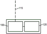
Fig. 1 shows a main schematic view of a first embodiment of a laser sensor module. The laser sensor module comprises a VCSEL100 and a driving circuit 120 for electrically driving the VCSEL 100. The driver circuit 120 is electrically connected to the VCSEL100 to provide electrical power to the VCSEL100 in a defined manner. The driver circuit 120 includes a memory device for storing data and instructions for operating the driver circuit 120 and a processing unit for executing data and instructions for operating the driver circuit 120. The driving circuit 120 includes a data interface for submitting and receiving data to and from an external device. The external device may be an evaluation unit for receiving information about the emitted laser light 115 or control parameters for driving the VCSEL. The external device may be a sensor, such as a thermocouple, which provides information about the ambient temperature that may be used to adapt the control parameters for driving the VCSEL. The driver circuit 120 may further be adapted to determine the state of the VCSEL by performing, for example, a resistance measurement in order to determine the temperature of the VCSEL during operation. The driving circuit 120 may further be adapted to measure, receive and analyze any information that may be relevant in order to determine a driving or pulsing scheme for operating the VCSEL100 in relation to the state of the VCSEL prior to or during operation.
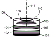
Fig. 2 shows a main schematic diagram of the layer structure of the VCSEL 100. The emitted laser light 115 is emitted via the substrate 105, which may be a gallium arsenide (GaAs) substrate. The VCSEL100 is thus a so-called bottom emitter. The VCSEL includes a first electrode 101 and a first Distributed Bragg Reflector (DBR) 102 mechanically coupled to the first electrode 101. The VCSEL further comprises an active layer 103, which is a semiconductor layer arrangement arranged between the first DBR102 and the second DBR 104. The first DBR102, the active region 103 and the second DBR define a laser cavity of the VCSEL100 in which laser light is generated. The second DBR104 is mechanically coupled to the substrate 105 of the VCSEL. A ring-shaped second electrode 106 is mechanically coupled to the top side of the substrate 105. It is also possible to provide, instead of the annular second electrode 106, an electrode layer in which holes are provided through which the laser light is emitted. Additional layers, not shown, may be present between the first electrode 101 and the first DBR102, between the first DBR102 and the active region 103, between the active region 103 and the second DBR104, between the second DBR104 and the substrate, and between the substrate 105 and the second electrode 106. Such a layer may be one or more oxide apertures, which may preferably be provided close to the active region 103 in order to confine the current. The oxide aperture may be, for example, circular, such that the diameter of the oxide aperture defines the laser aperture of the VCSEL. Ohmic losses of the current from the first electrode 101 to the second electrode 106 and optical losses caused by the emitted light directly heat the volume through which the current flows and the laser light is emitted. The surrounding volume of the VCSEL is indirectly heated by means of heat dissipation. The heat caused by losses and heat dissipation leads after a certain time to a smooth temperature profile or more precisely a smooth radial temperature gradient across the laser aperture, with the maximum temperature in the middle or center of the laser aperture and to a certain extent lower temperatures at the edges of the laser aperture. This temperature profile results in a variation of the refractive index within the material such that the thermal lens 140 is constructed. A basic description of the background of VCSELs and VECSELs and design choices, including the concept of thermal lenses, can be found in chapter 7 of "Semiconductor Disk Lasers" (o.ohkotnikov, Wiley press, 2010), which is incorporated herein by reference. The major portion of the thermal lens 140 is located in the substrate 105 of the bottom emitting VCSEL or VECSEL (v (e) CSEL). In case of top emission v (e) CSEL, the thermal lens will be located within the first DBR102 and the intermediate layer, which will be located between the first DBR102 and the first electrode 101. It is believed that the thermal lens 140 is necessary to define the choice of stable resonator and thus stable laser mode in order to allow accurate time of flight measurements. The change of the lens and thus the resonator due to the temperature change makes it more difficult to identify the emitted laser light 115, which is emitted by the VCSEL. In the case of a VECSEL, the situation is even worse, wherein the thermal lens 140 affects the optical feedback provided by the feedback element 130 (see fig. 3) and thus the time at which the VECSEL starts lasing.
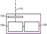
Fig. 3 shows a main schematic view of a second embodiment of a laser sensor module. The laser sensor module comprises a VCSEL100, a feedback element 130, which may be a mirror with a reflectivity of about 95%, and a driving circuit 120 for electrically driving the VCSEL 100. The VCSEL100 and the facet mirror constitute a VECSEL in which the laser cavity and the facet mirror constitute an extended cavity. The reflectivity of the second DBR104 is designed such that there is no lasing without feedback provided by the mirrors. The reflectivity of the mirrors required for lasing depends on the reflectivity of the second DBR and can vary over a wide range. VECSELs are mainly used for high power applications. The function of the driver circuit 120 is the same as discussed in relation to the first embodiment shown in fig. 1.
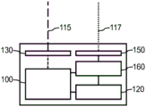
Fig. 4 shows a main schematic view of a first embodiment of the distance detection device. The distance detection device comprises a laser sensor module similar to the second embodiment discussed in relation to fig. 3. The distance detection device further comprises a light detector 150 and an evaluator 160. The light detector 150 is in this case a photodiode, but may preferably be any semiconductor device that can be used to detect the laser light emitted by the VECSEL. The light detector should be as sensitive as possible to the photons emitted by the laser and should have a fast measurement time. A preferred technology is e.g. avalanche photodiodes or even more so-called SPADs (single photon avalanche diodes) and arrays thereof. The evaluator 160 comprises at least one memory device like a memory chip and at least one processing device like a microprocessor. The processing device is adapted to receive data from the drive circuit 120 and optionally from the VCSEL100 in order to determine a time t at which the emitted laser light 115 leaves the extended cavity in the form of laser pulses 345 (see e.g. fig. 5) having a pulse length 356 (see e.g. fig. 5) of 5ns1. The evaluator 160 further bases the time t1And determining whether the photodiode detected reflected laser light 117 originates from the time t by means of the repetition rate provided by the drive circuit 1201To the emitted laser pulses. Recording the time t if the reflected laser light 117 originates from the laser pulse2And by means of the time of flight Δ t = t2-t1And the speed c of the laser pulse, the distance to the object reflecting the laser pulse is calculated. Taking into account the speed of the light, t1And t2Must be very accurate in order to allow accurate calculation of the distance to the object. Delays, in particular varying delays, between current pulses triggering the laser pulses must be avoided in order to allow an accurate determination of t1And is combined withAnd the laser pulses must be well defined in order to allow accurate determination of t2. In further embodiments, a pulse train, i.e. several laser pulses of different lengths and or different off-times, may be used.
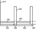
Fig. 5 shows a main schematic of a first embodiment of the pulse scheme. The pulse scheme is not drawn to scale. The pulse scheme comprises a pre-current 335 having a pulse length 352 such that, for the entire time between two laser pulses 345, a current is provided having a current amplitude below the laser threshold current 350 of the v (e) CSEL to which the pre-current 335 is provided. The laser threshold strongly depends on the design of the v (e) CSEL. The pre-current 335 is provided as an offset or bias current between the laser pulses 345 and therefore must be below the laser threshold in order to avoid lasing. The laser pulse 345 has a pulse length 356 of 20ns and is provided with a period of 10 μ s (100 kHz repetition frequency). It should be mentioned that in the discussion of fig. 5 and in the discussion of fig. 6 and 7, the current pulse triggering the laser pulse 345 and the laser pulse 345 are used synonymously. In fact, there are slight differences between the two, wherein it is an object of the present invention to minimize or even avoid these differences. The pre-current 335 is adapted such that a thermal lens 140 is formed at the beginning of each laser pulse 345.
The effect of the pre-current can be described approximately as follows. The temperature distribution as a function of space and time follows the solution of the differential equation of thermal conduction. One-dimensional solutions can be written as

It is substantially A spatial gaussian distribution of (a). Constant number
 Referred to as the temperature conductivity of the medium and is equal to the thermal conductivity lambda divided by the specific gravity and the heat capacity. In the case of GaAs, for example,a= 2.4E-5 m²/s。
this means that a temperature distribution in mobile GaAs costs about 10 μm for 1 μ s. In the case where the radius of V (E) CSEL is 50-100 [ mu ] m and the thickness of GaAs substrate is a similar value, it can be inferred that
The pulse length, e.g. 10-100 ns, is short compared to the temperature conduction, i.e. the heat deposited during the pulse defines the temperature distribution at t = 0.
Approximately 10 μ s is required to establish a smooth temperature distribution across the center of the maximum of the diameter of the laser aperture. (strictly speaking, after 10 μ s, σ is only about 20 μm, but this should be possible to get a smooth distribution from the top-hat temperature distribution at t = 0).
On a similar time scale, such a temperature profile is also established in the closer part of the substrate. The effective thermal lens 140 is related to the integral along the laser beam through all materials. A higher temperature in the center corresponds to a higher refractive index in the center.
Over time, such a smooth temperature distribution and thermal lens 140 is also established deeper in the substrate (but obviously, the absolute temperature difference or the lens is weaker). Larger volumes can be more compensated by reduced temperature differences and since the heat conduction is three-dimensional, these differences will decrease rapidly (in the n-dimensional case, the square root in the above equation is replaced by the exponent n/2). Therefore, the thermal lens 140 is expected to be largest after 1-10 μ s and to reach the average later.
Since the mesa of the v (e) CSEL is soldered to a heat sink at a typical distance of 5 μm from the active area 103, the heat loss of the heat sink to the substrate will significantly reduce all temperatures starting from 1 μ s after the pulse (the thermal and temperature conductivity in the heat sink is higher than in GaAs). This again emphasizes that after a few mus the thermal lens effect passes its maximum value.
After approximately 100 μ s, the effect of the thermal lens is expected to be small.
The details also depend on the heat loss and hence T (x, T = 0). If, for example, the losses have followed a gaussian shape, the thermal lens 140 may be established faster and the maximum value is reached at about 1 μ s. Furthermore, the diameter of the laser aperture of 50-100 μm may be smaller, so that the thermal lens may be established even within 100ns or hundreds of nanoseconds.
Returning to the pulse shape discussed with respect to fig. 5, this means that the thermal energy provided by means of the laser pulse 345 provides a major contribution to the formation of the thermal lens 140 in subsequent laser pulses. In case the time between two consecutive pulses is >1-10 μ s, this contribution is not sufficient, since the thermal energy is already spread over a large volume, requiring additional thermal energy. This additional energy is provided locally within the laser aperture by means of the offset current of the pre-current 335.
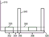
Fig. 6 shows a main schematic of a second embodiment of the pulse scheme. The pulse scheme is not drawn to scale. The pulse scheme includes a pre-current 335 provided as a current pre-pulse having a pulse length 352 that is shorter than the time between two laser pulses 345. There is a period of time after the laser pulse 345 and a time gap 354 before the subsequent laser pulse in which no current is supplied to the v (e) CSEL. The current pre-pulse has a current amplitude of 95% (1 amp current at 3 volts) of the laser threshold current 350 of the v (e) CSEL to which the pre-current 335 is supplied. The laser pulse 345 has a pulse length 356 of 2ns and is provided with a period (50 kHz repetition frequency) of 20 μ s. The pulse length 352 of the current pre-pulse is 3 μ s and the time gap is 50 ns. The total thermal energy provided by means of the current pre-pulse is 9 μ J, which is sufficient to heat an isolated table top of V (E) CSEL of, for example, 210 μm in diameter and a laser aperture of approximately 150 μm by approximately 60 Kelvin. The length and timing of the current pre-pulse is adapted to the physical structure of the v (e) CSEL and the length and repetition rate of the laser pulses 345.
A typical range of current amplitudes of the laser pulses is between 1A and 30A, preferably between 3A and 20A. A typical range of the current amplitude of the pre-current is between 0.01A and 5A, preferably between 0.1A and 2A. The ratio between the current amplitude of the laser pulses and the current amplitude of the pre-current should be larger than 2, preferably larger than 5. The pulse length 352 of the laser pulse 345 is between 1ns and 100ns, preferably between 2ns and 10 ns. The pulse length 356 of the pre-current 335 is between 10ns and 10000ns, preferably between 100ns and 5000 ns. The time gap 355 is between 0ns and 1000 ns. The time period between laser pulses is preferably between 1 and 20 mus, more preferably between 2 and 10 mus. For a VECSEL of relatively large diameter (> 100 μm), the thermal energy required to create the thermal lens is preferably >1 μ J, more preferably >3 μ J.
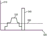
Fig. 7 shows a main schematic of a third embodiment of the pulse scheme supplied to the VECSEL. The pre-current 335 is provided as a complex current pre-pulse in which the current amplitude is quickly above the laser threshold. The time period above the laser threshold is so short that there is no time to establish the thermal lens 140. Thus, laser emission of the VECSEL is avoided during this period.
Fig. 8 shows a main schematic view of a second embodiment of the distance detection device. The general configuration of the distance detection device is similar to that of the distance detection device as discussed in relation to fig. 4. The distance detection device comprises an evaluator 160 and a drive circuit 120 operating in a similar manner as described above. The driver circuitry 120 and the evaluator 160 are integrated into a mounting structure 200 on which a two-dimensional array of v (e) CSELs 100 and light detectors 150 is arranged. V (e) CSEL provides emitted laser light 115 via mirror 210 and scan mirror 220. The reflected laser light is received by means of the light detector 150 via the scanning mirror 220 and the mirror 210. The scanning mirror 210 is a MEMS mirror so that the emitted laser light 115 of different v (e) CSELs can all be emitted to different areas to provide 3D information about the distance to an object in the context of a distance detection device that can be mounted on a vehicle such as an automobile. The drive circuit 120 provides a pre-current 335 to the v (e) CSELs that is adapted to the relative position of the individual v (e) CSELs (e.g., the center or edge of the array 200). The pre-current 335 or current pre-pulse is further adapted to cause the v (e) CSELs of the array 200 controlled by the driver circuit 120 to emit laser light 345 simultaneously to start the laser emission within a predefined time period. The predefined time period is related to thermal cross-talk between adjacent v (e) CSELs that are controlled to emit laser pulses simultaneously. The current pre-pulse is adapted to have a duration that is just long enough to establish a smooth temperature gradient across the laser aperture, but short enough (and not separated in time) to minimize thermal cross-talk between adjacent mesas, especially of the v (e) CSEL.
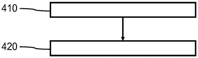
FIG. 9 illustrates a main schematic of one embodiment of a method of driving a laser sensor module. In step 410, electrical energy is provided to the vertical cavity surface emitting laser such that the vertical cavity surface emitting laser emits laser pulses having a pulse length of less than 100ns and a repetition rate of less than 5% compared to continuous laser emission. In step 420, additional energy is provided to the vertical cavity surface emitting laser at least 100ns before at least the portion of the laser pulse such that the portion of the laser pulse is emitted under defined optical conditions.
It is an object of the present invention to allow reliable time-of-flight distance measurement by means of v (e) CSEL100 or v (e) CSEL array 200. A thermal lens 140 is provided near the laser aperture by means of the additional energy. This additional energy is preferably provided by means of a current pre-pulse 335 applied to the v (e) CSEL prior to preferably each laser pulse 345. The current pre-pulse is preferably arranged such that no laser light is emitted by means of the v (e) CSEL. Under defined optical conditions, the v (e) CSEL is allowed to emit the laser pulse 345 such that the emission time and pulse shape of the laser pulse 345 are well defined. The well-defined emission time and the well-defined pulse shape of the laser pulses 345 allow for a reliable detection of the reflected laser light 117, which corresponds to the emission of the corresponding laser pulses 345.
While the invention has been illustrated and described in detail in the drawings and foregoing description, such illustration and description are to be considered illustrative or exemplary and not restrictive.
Other modifications will be apparent to persons skilled in the art upon reading this disclosure. Such modifications may involve other features which are already known in the art and which may be used instead of or in addition to features already described herein.
Variations to the disclosed embodiments can be understood and effected by those skilled in the art, from a study of the drawings, the disclosure, and the appended claims. In the claims, the word "comprising" does not exclude other elements or steps, and the indefinite article "a" or "an" does not exclude a plurality of elements or steps. The mere fact that certain measures are recited in mutually different dependent claims does not indicate that a combination of these measures cannot be used to advantage.
Any reference signs in the claims shall not be construed as limiting the scope.
List of reference numerals
100 VCSEL
101 first electrode
102 first DBR
103 active region
104 second DBR
105 substrate
106 second electrode
115 emitted laser light
117 reflected laser light
120 drive circuit
130 feedback element
140 thermal lens
150 photo detector
160 estimator
200 array
210 mirror
220 scanning mirror
230 mounting structure
310 strength
320 hours
335 pre-current
345 laser pulses
350 laser threshold current
Pulse length of 352 current pre-pulse
354 time gap
356 pulse length of laser pulse
358 time period between two laser pulses
410 providing laser pulses
420 provide a current pre-pulse
Claims (17)
1. A laser sensor module for time-of-flight measurements, comprising at least one vertical cavity surface emitting laser (100) and at least one driving circuit (120), the driving circuit (120) being adapted to supply electrical energy to the vertical cavity surface emitting laser (100) such that the vertical cavity surface emitting laser (100) emits laser pulses (345) having a pulse length (356) of less than 100ns and a duty cycle of less than 5% compared to continuous laser emission, wherein the driving circuit (120) is adapted to supply additional energy to the vertical cavity surface emitting laser (100) at least 100ns before at least a part of said laser pulses (345) such that the part of said laser pulses (345) are emitted under defined optical conditions, wherein the driving circuit (120) is adapted to supply a pre-current (335) to the vertical cavity surface emitting laser (100), wherein no laser emission precedes the part of said laser pulses (345), wherein the pre-current (335) is adapted such that a smooth temperature profile is established across the laser aperture of the vertical cavity surface emitting laser (100) such that the thermal lens (140) is formed at the laser aperture.
2. The laser sensor module according to claim 1, wherein the vertical cavity surface emitting laser (100) is arranged to operate in a stable mode during time-of-flight measurements.
3. The laser sensor module according to claim 2, wherein the vertical cavity surface emitting laser (100) is arranged to operate in a fundamental mode during time-of-flight measurements.
4. The laser sensor module according to claim 1, wherein the temperature difference between the center of the laser aperture and the edge of the laser aperture at the beginning of the emission of the portion of the laser pulse (345) is at least 2K.
5. The laser sensor module according to claim 1, wherein the temperature difference between the center of the laser aperture and the edge of the laser aperture at the beginning of the emission of the portion of the laser pulse (345) is at least 5K.
6. The laser sensor module according to claim 1, wherein the temperature difference between the center of the laser aperture and the edge of the laser aperture at the beginning of the emission of the portion of the laser pulse (345) is at least 10K.
7. The laser sensor module according to claim 1, wherein the pre-current (335) comprises a constant offset current provided between two laser pulses (345).
8. The laser sensor module according to claim 1, wherein the pre-current (335) comprises at least one current pre-pulse between two subsequent laser pulses (345).
9. The laser sensor module according to claim 8, wherein the drive circuit (120) is adapted to provide a time gap (354) of at least 10ns between the current pre-pulse and a laser pulse (345) emitted after the current pre-pulse is provided to the vertical cavity surface emitting laser (100), wherein the peak current is less than 50% of a laser threshold current of the vertical cavity surface emitting laser (100).
10. The laser sensor module according to claim 8, wherein the current pre-pulse comprises a maximum current amplitude above a laser threshold current of the vertical cavity surface emitting laser (100).
11. The laser sensor module according to any of the claims 4 to 10, wherein the vertical cavity surface emitting laser (100) comprises at least one thermal management structure adapted to establish a smooth temperature profile across the laser aperture of the vertical cavity surface emitting laser (100) between two subsequent laser pulses (345), wherein the thermal management structure is arranged to increase heat removal at the edges of the laser aperture compared to the center of the laser aperture.
12. The laser sensor module according to claim 1, wherein the vertical cavity surface emitting laser (100) is a vertical extended cavity surface emitting laser comprising an optical feedback element.
13. The laser sensor module according to claim 1, comprising an array of vertical cavity surface emitting lasers (100), wherein the driving circuit (120) is adapted to provide a pre-current (335) to at least a part of the vertical cavity surface emitting lasers (100) of the array, and wherein the pre-current (335) is adapted to the relative position within the array of the vertical cavity surface emitting lasers (100) to which the pre-current (335) is provided, such that different pre-currents (335) are provided to at least a first and a second vertical cavity surface emitting laser (100) of the array.
14. The laser sensor module according to claim 8, comprising an array of vertical cavity surface emitting lasers (100), wherein the driving circuit (120) is adapted to provide a current pre-pulse to at least a part of the vertical cavity surface emitting lasers (100) of the array, and wherein the current pre-pulse is adapted to cause a vertical cavity surface emitting laser (100) controlled by the driving circuit (120) to emit laser pulses (345) simultaneously to start lasing within a predefined time period related to thermal cross talk between neighboring vertical cavity surface emitting lasers (100) controlled to emit laser pulses (345) simultaneously.
15. A distance detection device comprising at least one laser sensor module according to any one of claims 1 to 14, at least one light detector (150) adapted to receive reflected laser light of at least one laser pulse (345), the distance detection device further comprising an evaluator (160), the evaluator (160) being adapted to identify reflected laser light of a respective laser pulse (345), and the evaluator (160) being further adapted to determine a time of flight between a time of reception of the reflected laser light and a time of emission of the respective laser pulse (345).
16. A method of driving a laser sensor module for time-of-flight measurements, the laser sensor module comprising at least one vertical cavity surface emitting laser (100), the method comprising the steps of:
-providing electrical energy to the vertical cavity surface emitting laser (100) such that the vertical cavity surface emitting laser (100) emits laser pulses (345) having a pulse length (356) of less than 100ns and a repetition rate of less than 5% compared to continuous laser emission;
-providing additional energy to a vertical cavity surface emitting laser (100) by means of a pre-current (335) at least 100ns before at least a part of the laser pulse (345), wherein no laser emission precedes the part of the laser pulse such that the part of the laser pulse (345) is emitted under defined optical conditions;
-adapting the pre-current (335) such that a smooth temperature profile is established across the laser aperture of the vertical cavity surface emitting laser (100) such that the thermal lens (140) is formed at the laser aperture.
17. The method according to claim 16, wherein the method comprises the additional step of:
-determining a first thermal energy generated in the vertical cavity surface emitting laser (100) during emission of the laser pulse (345);
-determining additional energy to be provided;
-determining a pulse shape of the pre-current (335) based on the determined additional energy.
Applications Claiming Priority (3)
| Application Number | Priority Date | Filing Date | Title |
|---|---|---|---|
| EP14199083 | 2014-12-19 | ||
| EP14199083.8 | 2014-12-19 | ||
| PCT/EP2015/079396 WO2016096647A1 (en) | 2014-12-19 | 2015-12-11 | Laser sensor module |
Publications (2)
| Publication Number | Publication Date |
|---|---|
| CN107005023A CN107005023A (en) | 2017-08-01 |
| CN107005023B true CN107005023B (en) | 2020-03-24 |
Family
ID=52144466
Family Applications (1)
| Application Number | Title | Priority Date | Filing Date |
|---|---|---|---|
| CN201580069482.9A Active CN107005023B (en) | 2014-12-19 | 2015-12-11 | Laser sensor module |
Country Status (7)
| Country | Link |
|---|---|
| US (1) | US10680411B2 (en) |
| EP (1) | EP3235078B1 (en) |
| JP (1) | JP6849593B2 (en) |
| CN (1) | CN107005023B (en) |
| BR (1) | BR112017012605A2 (en) |
| RU (1) | RU2696335C2 (en) |
| WO (1) | WO2016096647A1 (en) |
Families Citing this family (16)
| Publication number | Priority date | Publication date | Assignee | Title |
|---|---|---|---|---|
| EP3493339B1 (en) | 2017-12-04 | 2022-11-09 | ams AG | Semiconductor device and method for time-of-flight and proximity measurements |
| EP3517998B1 (en) * | 2018-01-24 | 2023-12-06 | Leica Geosystems AG | Airborne lidar pulse rate modulation |
| EP3540879A1 (en) * | 2018-03-15 | 2019-09-18 | Koninklijke Philips N.V. | Vertical cavity surface emitting laser device with integrated tunnel junction |
| WO2019227975A1 (en) | 2018-05-30 | 2019-12-05 | Oppo广东移动通信有限公司 | Control system of laser projector, terminal and control method of laser projector |
| CN108963750B (en) * | 2018-07-18 | 2023-08-29 | 度亘激光技术(苏州)有限公司 | VCSEL and APD integrated chip and preparation method thereof |
| WO2021158176A1 (en) * | 2020-02-07 | 2021-08-12 | Ams Sensors Asia Pte. Ltd. | Sensing method and sensor system |
| US11594852B2 (en) * | 2020-05-08 | 2023-02-28 | Microsoft Technology Licensing, Llc | Pulse shaping to reduce pulse history effects in pulsed lasers |
| US11500093B2 (en) | 2021-03-26 | 2022-11-15 | Aeye, Inc. | Hyper temporal lidar using multiple matched filters to determine target obliquity |
| US11474214B1 (en) | 2021-03-26 | 2022-10-18 | Aeye, Inc. | Hyper temporal lidar with controllable pulse bursts to resolve angle to target |
| US20220308184A1 (en) | 2021-03-26 | 2022-09-29 | Aeye, Inc. | Hyper Temporal Lidar with Controllable Detection Intervals |
| US11635495B1 (en) | 2021-03-26 | 2023-04-25 | Aeye, Inc. | Hyper temporal lidar with controllable tilt amplitude for a variable amplitude scan mirror |
| US11474213B1 (en) | 2021-03-26 | 2022-10-18 | Aeye, Inc. | Hyper temporal lidar with dynamic laser control using marker shots |
| US11630188B1 (en) * | 2021-03-26 | 2023-04-18 | Aeye, Inc. | Hyper temporal lidar with dynamic laser control using safety models |
| US11604264B2 (en) | 2021-03-26 | 2023-03-14 | Aeye, Inc. | Switchable multi-lens Lidar receiver |
| JP2023116281A (en) * | 2022-02-09 | 2023-08-22 | 株式会社小糸製作所 | Floodlight and measurement apparatus |
| DE102022103899A1 (en) | 2022-02-18 | 2023-08-24 | Schwind Eye-Tech-Solutions Gmbh | Treatment device for eye treatment, method, computer program and computer-readable medium |
Citations (1)
| Publication number | Priority date | Publication date | Assignee | Title |
|---|---|---|---|---|
| CN102208907A (en) * | 2010-03-31 | 2011-10-05 | 索尼公司 | Correction circuit, drive circuit, light-emitting device and correction method of current pulse waveform |
Family Cites Families (20)
| Publication number | Priority date | Publication date | Assignee | Title |
|---|---|---|---|---|
| US6243407B1 (en) * | 1997-03-21 | 2001-06-05 | Novalux, Inc. | High power laser devices |
| US6751245B1 (en) | 1999-06-02 | 2004-06-15 | Optical Communication Products, Inc. | Single mode vertical cavity surface emitting laser |
| JP2001315381A (en) * | 2000-05-11 | 2001-11-13 | Fuji Photo Film Co Ltd | Method and apparatus for recording image on photosensitive thermal recording material |
| DE10038235A1 (en) * | 2000-08-04 | 2002-02-21 | Osram Opto Semiconductors Gmbh | Surface emitting laser with side current injection |
| US6636539B2 (en) | 2001-05-25 | 2003-10-21 | Novalux, Inc. | Method and apparatus for controlling thermal variations in an optical device |
| US6834065B2 (en) | 2002-05-21 | 2004-12-21 | Carrier Access Corporation | Methods and apparatuses for direct digital drive of a laser in a passive optical network |
| EP1517415A1 (en) * | 2003-09-18 | 2005-03-23 | Leica Geosystems AG | Geodetic apparatus with laser source |
| JP4432459B2 (en) | 2003-10-30 | 2010-03-17 | 日亜化学工業株式会社 | Semiconductor laser diode driving method and light emitting device |
| JP2008535263A (en) * | 2005-03-30 | 2008-08-28 | ノバラックス,インコーポレイティド | Vertically stabilized cavity surface emitting laser with frequency stabilization |
| JP2007311616A (en) * | 2006-05-19 | 2007-11-29 | Seiko Epson Corp | Surface-emitting light source and manufacturing method thereof |
| CN101517520B (en) | 2006-10-03 | 2014-11-19 | 皇家飞利浦电子股份有限公司 | Laser controller |
| EP2189806B1 (en) | 2008-11-20 | 2011-05-18 | Sick Ag | Optoelectronic sensor |
| JP5257053B2 (en) * | 2008-12-24 | 2013-08-07 | 株式会社豊田中央研究所 | Optical scanning device and laser radar device |
| US8995485B2 (en) * | 2009-02-17 | 2015-03-31 | Trilumina Corp. | High brightness pulsed VCSEL sources |
| JP2011216843A (en) | 2010-03-16 | 2011-10-27 | Ricoh Co Ltd | Semiconductor laser driving unit, and image forming apparatus including the same |
| JP2012209501A (en) * | 2011-03-30 | 2012-10-25 | Sony Corp | Correction circuit, driving circuit, light emitting apparatus, and method of correcting electric current pulse waveform |
| US20150288145A1 (en) * | 2012-01-25 | 2015-10-08 | Hewlett-Packard Development Company, L.P. | Vertical-cavity surface-emitting lasers with non-periodic gratings |
| JP5949411B2 (en) * | 2012-10-04 | 2016-07-06 | ソニー株式会社 | Correction circuit, drive circuit, light-emitting device, and current pulse waveform correction method |
| US9413137B2 (en) | 2013-03-15 | 2016-08-09 | Nlight, Inc. | Pulsed line beam device processing systems using laser diodes |
| US9069080B2 (en) | 2013-05-24 | 2015-06-30 | Advanced Scientific Concepts, Inc. | Automotive auxiliary ladar sensor |
-
2015
- 2015-12-11 RU RU2017125504A patent/RU2696335C2/en not_active IP Right Cessation
- 2015-12-11 CN CN201580069482.9A patent/CN107005023B/en active Active
- 2015-12-11 EP EP15808581.1A patent/EP3235078B1/en active Active
- 2015-12-11 BR BR112017012605-2A patent/BR112017012605A2/en not_active Application Discontinuation
- 2015-12-11 JP JP2017532026A patent/JP6849593B2/en active Active
- 2015-12-11 US US15/536,905 patent/US10680411B2/en active Active
- 2015-12-11 WO PCT/EP2015/079396 patent/WO2016096647A1/en active Application Filing
Patent Citations (1)
| Publication number | Priority date | Publication date | Assignee | Title |
|---|---|---|---|---|
| CN102208907A (en) * | 2010-03-31 | 2011-10-05 | 索尼公司 | Correction circuit, drive circuit, light-emitting device and correction method of current pulse waveform |
Non-Patent Citations (2)
| Title |
|---|
| Spatial decoherence of pulsed broad-area vertical-cavity surface-emitting lasers;Michael Peeters et al;《Optics Express》;20051114;第13卷(第23期);第9337-9344页,图5 * |
| Thermally controlled onset of spatially incoherent emission in a broad-area vertical-cavity surface-emitting laser;Gordon Craggs, et al.;《IEEE Journal of Selected Optics in Quantum Electronics》;20090605;第15卷(第3期);第555-562页 * |
Also Published As
| Publication number | Publication date |
|---|---|
| WO2016096647A1 (en) | 2016-06-23 |
| RU2017125504A (en) | 2019-01-21 |
| JP6849593B2 (en) | 2021-03-24 |
| US10680411B2 (en) | 2020-06-09 |
| JP2018505548A (en) | 2018-02-22 |
| RU2696335C2 (en) | 2019-08-01 |
| CN107005023A (en) | 2017-08-01 |
| RU2017125504A3 (en) | 2019-05-22 |
| EP3235078B1 (en) | 2022-02-02 |
| US20190097393A1 (en) | 2019-03-28 |
| BR112017012605A2 (en) | 2018-01-16 |
| EP3235078A1 (en) | 2017-10-25 |
Similar Documents
| Publication | Publication Date | Title |
|---|---|---|
| CN107005023B (en) | Laser sensor module | |
| EP3443383B1 (en) | Distance measuring device and method thereof | |
| CN110892596B (en) | Vertical Cavity Surface Emitting Laser (VCSEL) with improved gain switching characteristics | |
| JP6340852B2 (en) | Distance measuring device, moving body, and distance measuring method | |
| CN111742238A (en) | Laser arrangement with a filter | |
| EP3496216A1 (en) | Segmented vertical cavity surface emitting laser | |
| EP1173907A1 (en) | Semiconductor diode lasers with thermal sensor control of the active region temperature | |
| Slipchenko et al. | High-Power and Repetion Rate Nanosecond Pulse Generation in “Diode Laser—Thyristor” Stacks | |
| EP3176888A1 (en) | Sensor chip | |
| Ammouri et al. | Wavelength‐stabilized ns‐pulsed 2.2 kW diode laser bar with multiple active regions and tunnel junctions | |
| JP2016014577A (en) | Distance measurement device, mobile entity, and distance measurement method | |
| US20220115836A1 (en) | Light-emitting device, optical device, and information processing device | |
| US20210302540A1 (en) | Light-emitting device, optical device, measurement device, and information processing apparatus | |
| Crump et al. | Joule-class 940-nm diode laser bars for millisecond pulse applications | |
| Herper et al. | VECSEL for 3D LiDAR applications | |
| US20240136793A1 (en) | Surface-emitting laser, laser device, detection device, mobile object, and method for driving surface-emitting laser | |
| US20240085534A1 (en) | Light emitting device, ranging device and movable object | |
| EP4358326A1 (en) | Surface-emitting laser, laser device, detection device, mobile object, and method for driving surface-emitting laser | |
| US10535976B1 (en) | Optical device and system having thermal buffers | |
| Grabherr et al. | New markets for VCSELS: pulsed operation of high-power devices | |
| US20230307886A1 (en) | Wavelength stabilization of pulsed lasers | |
| CN117321868A (en) | Light emitting device, distance measuring device, and moving object | |
| CN117795793A (en) | Surface-emitting laser, laser device, detection device, moving body, and surface-emitting laser driving method | |
| Zaitsev et al. | Superradiance in semiconductors |
Legal Events
| Date | Code | Title | Description |
|---|---|---|---|
| PB01 | Publication | ||
| PB01 | Publication | ||
| SE01 | Entry into force of request for substantive examination | ||
| SE01 | Entry into force of request for substantive examination | ||
| GR01 | Patent grant | ||
| GR01 | Patent grant | ||
| TR01 | Transfer of patent right |
Effective date of registration: 20200624 Address after: Ulm Patentee after: Tongkuai optoelectronic device Co.,Ltd. Address before: Eindhoven, Netherlands Patentee before: KONINKLIJKE PHILIPS N.V. |
|
| TR01 | Transfer of patent right |