CN106054588B - Communication system, electronic timepiece, and communication device - Google Patents
Communication system, electronic timepiece, and communication device Download PDFInfo
- Publication number
- CN106054588B CN106054588B CN201610185038.XA CN201610185038A CN106054588B CN 106054588 B CN106054588 B CN 106054588B CN 201610185038 A CN201610185038 A CN 201610185038A CN 106054588 B CN106054588 B CN 106054588B
- Authority
- CN
- China
- Prior art keywords
- electronic timepiece
- communication
- coil
- signal
- unit
- Prior art date
- Legal status (The legal status is an assumption and is not a legal conclusion. Google has not performed a legal analysis and makes no representation as to the accuracy of the status listed.)
- Active
Links
- 230000006854 communication Effects 0.000 title claims abstract description 380
- 238000004891 communication Methods 0.000 title claims abstract description 362
- 230000005540 biological transmission Effects 0.000 claims abstract description 105
- 238000001514 detection method Methods 0.000 claims abstract description 45
- 230000008878 coupling Effects 0.000 claims abstract description 24
- 238000010168 coupling process Methods 0.000 claims abstract description 24
- 238000005859 coupling reaction Methods 0.000 claims abstract description 24
- 230000003287 optical effect Effects 0.000 claims abstract description 9
- 238000012545 processing Methods 0.000 claims description 90
- 239000011521 glass Substances 0.000 claims description 24
- 230000015654 memory Effects 0.000 claims description 20
- 230000005611 electricity Effects 0.000 claims 1
- 238000010586 diagram Methods 0.000 description 32
- 238000000034 method Methods 0.000 description 29
- 238000003860 storage Methods 0.000 description 27
- 230000007246 mechanism Effects 0.000 description 25
- 230000008054 signal transmission Effects 0.000 description 24
- 230000008569 process Effects 0.000 description 21
- 230000008859 change Effects 0.000 description 17
- 239000000758 substrate Substances 0.000 description 11
- 230000006870 function Effects 0.000 description 10
- 230000004048 modification Effects 0.000 description 10
- 238000012986 modification Methods 0.000 description 10
- NJPPVKZQTLUDBO-UHFFFAOYSA-N novaluron Chemical compound C1=C(Cl)C(OC(F)(F)C(OC(F)(F)F)F)=CC=C1NC(=O)NC(=O)C1=C(F)C=CC=C1F NJPPVKZQTLUDBO-UHFFFAOYSA-N 0.000 description 9
- RYGMFSIKBFXOCR-UHFFFAOYSA-N Copper Chemical compound [Cu] RYGMFSIKBFXOCR-UHFFFAOYSA-N 0.000 description 7
- 230000017525 heat dissipation Effects 0.000 description 6
- 230000002093 peripheral effect Effects 0.000 description 5
- 238000013500 data storage Methods 0.000 description 4
- 238000005286 illumination Methods 0.000 description 4
- 229910000859 α-Fe Inorganic materials 0.000 description 4
- 239000000919 ceramic Substances 0.000 description 3
- 239000004973 liquid crystal related substance Substances 0.000 description 3
- 238000004519 manufacturing process Methods 0.000 description 3
- 239000002184 metal Substances 0.000 description 3
- 229910052751 metal Inorganic materials 0.000 description 3
- 238000003825 pressing Methods 0.000 description 3
- 238000012790 confirmation Methods 0.000 description 2
- 238000012937 correction Methods 0.000 description 2
- 230000000694 effects Effects 0.000 description 2
- 238000005401 electroluminescence Methods 0.000 description 2
- 230000001678 irradiating effect Effects 0.000 description 2
- 239000000463 material Substances 0.000 description 2
- 238000010248 power generation Methods 0.000 description 2
- 239000010453 quartz Substances 0.000 description 2
- VYPSYNLAJGMNEJ-UHFFFAOYSA-N silicon dioxide Inorganic materials O=[Si]=O VYPSYNLAJGMNEJ-UHFFFAOYSA-N 0.000 description 2
- 230000001360 synchronised effect Effects 0.000 description 2
- HBBGRARXTFLTSG-UHFFFAOYSA-N Lithium ion Chemical compound [Li+] HBBGRARXTFLTSG-UHFFFAOYSA-N 0.000 description 1
- 230000002457 bidirectional effect Effects 0.000 description 1
- 230000000903 blocking effect Effects 0.000 description 1
- 239000006059 cover glass Substances 0.000 description 1
- 238000005520 cutting process Methods 0.000 description 1
- 235000012489 doughnuts Nutrition 0.000 description 1
- 239000000428 dust Substances 0.000 description 1
- 230000005674 electromagnetic induction Effects 0.000 description 1
- 230000005669 field effect Effects 0.000 description 1
- 238000003780 insertion Methods 0.000 description 1
- 230000037431 insertion Effects 0.000 description 1
- 229910001416 lithium ion Inorganic materials 0.000 description 1
- 238000005259 measurement Methods 0.000 description 1
- 239000004570 mortar (masonry) Substances 0.000 description 1
- 230000010355 oscillation Effects 0.000 description 1
- 230000004044 response Effects 0.000 description 1
Images


Classifications
-
- H04B5/26—
-
- H—ELECTRICITY
- H04—ELECTRIC COMMUNICATION TECHNIQUE
- H04B—TRANSMISSION
- H04B10/00—Transmission systems employing electromagnetic waves other than radio-waves, e.g. infrared, visible or ultraviolet light, or employing corpuscular radiation, e.g. quantum communication
- H04B10/80—Optical aspects relating to the use of optical transmission for specific applications, not provided for in groups H04B10/03 - H04B10/70, e.g. optical power feeding or optical transmission through water
-
- G—PHYSICS
- G04—HOROLOGY
- G04G—ELECTRONIC TIME-PIECES
- G04G21/00—Input or output devices integrated in time-pieces
- G04G21/04—Input or output devices integrated in time-pieces using radio waves
-
- G—PHYSICS
- G04—HOROLOGY
- G04G—ELECTRONIC TIME-PIECES
- G04G3/00—Producing timing pulses
- G04G3/02—Circuits for deriving low frequency timing pulses from pulses of higher frequency
-
- G—PHYSICS
- G04—HOROLOGY
- G04R—RADIO-CONTROLLED TIME-PIECES
- G04R20/00—Setting the time according to the time information carried or implied by the radio signal
- G04R20/02—Setting the time according to the time information carried or implied by the radio signal the radio signal being sent by a satellite, e.g. GPS
-
- G—PHYSICS
- G04—HOROLOGY
- G04R—RADIO-CONTROLLED TIME-PIECES
- G04R20/00—Setting the time according to the time information carried or implied by the radio signal
- G04R20/26—Setting the time according to the time information carried or implied by the radio signal the radio signal being a near-field communication signal
- G04R20/28—Tuning or receiving; Circuits therefor
-
- G—PHYSICS
- G04—HOROLOGY
- G04R—RADIO-CONTROLLED TIME-PIECES
- G04R20/00—Setting the time according to the time information carried or implied by the radio signal
- G04R20/26—Setting the time according to the time information carried or implied by the radio signal the radio signal being a near-field communication signal
- G04R20/30—Decoding time data; Circuits therefor
-
- G—PHYSICS
- G08—SIGNALLING
- G08C—TRANSMISSION SYSTEMS FOR MEASURED VALUES, CONTROL OR SIMILAR SIGNALS
- G08C19/00—Electric signal transmission systems
- G08C19/16—Electric signal transmission systems in which transmission is by pulses
Landscapes
- Physics & Mathematics (AREA)
- General Physics & Mathematics (AREA)
- Engineering & Computer Science (AREA)
- Computer Networks & Wireless Communication (AREA)
- Signal Processing (AREA)
- Electromagnetism (AREA)
- Radar, Positioning & Navigation (AREA)
- Remote Sensing (AREA)
- Electric Clocks (AREA)
- Power Engineering (AREA)
- Electromechanical Clocks (AREA)
Abstract
The invention provides a communication system, an electronic timepiece, and a communication device. One of an electronic timepiece and a communication device included in a communication system includes a 1 st communication unit, and the other includes a 2 nd communication unit. The 1 st communication unit includes: a coil transmission unit that includes a transmission coil and a drive circuit for driving the transmission coil, and transmits a signal by electromagnetic coupling-based communication using the transmission coil; and a light receiving unit which is provided with a light receiving element and a detection circuit for detecting an output value of the light receiving element, and receives a signal by optical communication using the light receiving element. The 2 nd communication unit includes: a light transmission unit that includes a light emitting element and a drive circuit for driving the light emitting element, and transmits a signal by light-based communication using the light emitting element; and a coil receiving unit which is provided with a receiving coil and a detection circuit for detecting an output value of the receiving coil, and receives a signal by communication based on electromagnetic coupling using the receiving coil.
Description
Technical Field
The present invention relates to a communication system, an electronic timepiece, and a communication device that process data.
Background
Conventionally, there is an electronic timepiece configured as follows: in order to update stored control data and the like, non-contact communication with an external device is possible (see, for example, patent document 1).
The analog electronic timepiece of patent document 1 includes a motor coil, and transmits a confirmation signal to an external adjustment device via the motor coil. The external adjustment device receives the confirmation signal via the coil, and then transmits correction data for adjusting the rate of change (step) of the analog electronic timepiece to the analog electronic timepiece via the coil. The analog electronic timepiece receives the correction data via the motor coil.
Patent document 1: japanese patent laid-open publication No. 2000-321378
Disclosure of Invention
The analog electronic timepiece of patent document 1 can transmit and receive signals to and from an external adjustment device, but only has one communication path by electromagnetic coupling using a coil with the external adjustment device, and therefore, it is necessary to switch between transmission and reception. Therefore, when the transmission and reception of the signal are repeated, there is a problem that the communication time becomes long.
The invention aims to provide a communication system, an electronic timepiece and a communication device, which can transmit and receive signals between the electronic timepiece and an external device and can accelerate communication processing.
The present invention is a communication system including an electronic timepiece and a communication device, one of the electronic timepiece and the communication device including a 1 st communication unit, the other of the electronic timepiece and the communication device including a 2 nd communication unit capable of communicating with the 1 st communication unit, the 1 st communication unit including: a coil transmission unit that includes a transmission coil and a drive circuit that drives the transmission coil, and that transmits a signal by electromagnetic coupling-based communication using the transmission coil; and a light receiving unit which includes a light receiving element and a detection circuit for detecting an output value of the light receiving element, and receives a signal by optical communication using the light receiving element, wherein the 2 nd communication unit includes: a light transmission unit that includes a light emitting element and a drive circuit that drives the light emitting element, and transmits a signal by light-based communication using the light emitting element; and a coil receiving unit that includes a receiving coil and a detection circuit that detects an output value of the receiving coil, and receives a signal by communication based on electromagnetic coupling using the receiving coil.
According to the present invention, for example, when the electronic timepiece includes the 1 st communication unit and the communication device includes the 2 nd communication unit, the signal transmitted by the coil transmission unit of the electronic timepiece is received by the coil reception unit of the communication device. In addition, the light receiving unit of the electronic timepiece receives the signal transmitted by the light transmitting unit of the communication device.
In addition, when the electronic timepiece includes the 2 nd communication unit and the communication device includes the 1 st communication unit, the signal transmitted by the light transmission unit of the electronic timepiece is received by the light reception unit of the communication device. In addition, the coil receiving unit of the electronic timepiece receives the signal transmitted by the coil transmitting unit of the communication device.
According to the present invention, since the communication path for transmitting a signal from the electronic timepiece to the communication device and the communication path for transmitting a signal from the communication device to the electronic timepiece are constituted by 2 paths having different communication methods from each other, the signal transmitted from the electronic timepiece to the communication device and the signal transmitted from the communication device to the electronic timepiece do not interfere with each other. Further, since it is not necessary to perform switching processing as in the case of switching the transmission direction of the signal and using 1 communication path, it is possible to speed up the communication processing between the electronic timepiece and the communication device.
An electronic timepiece according to the present invention includes: a coil transmission unit that includes a transmission coil and a drive circuit that drives the transmission coil, and that transmits a signal by electromagnetic coupling-based communication using the transmission coil; and a light receiving unit which is provided with a light receiving element and a detection circuit for detecting an output value of the light receiving element, and receives a signal by optical communication using the light receiving element.
According to the present invention, since the communication path for transmitting signals and the communication path for receiving signals are constituted by 2 paths having different communication methods, the transmitted signals and the received signals do not interfere with each other even in a small-sized timepiece such as a wristwatch in which the coil transmitting unit and the light receiving unit are disposed close to each other. Further, since it is not necessary to perform switching processing as in the case of switching 1 communication path for use in transmission and reception, it is possible to speed up the communication processing with the communication device.
Since the transmission unit is formed of a transmission coil, for example, a motor coil or the like provided in an electronic timepiece can be used as the transmission coil. In this case, it is not necessary to additionally provide a transmission coil, and an increase in the number of components can be suppressed.
In the electronic timepiece according to the present invention, it is preferable that the electronic timepiece includes a solar cell that receives light and generates electric power, and the light receiving element is constituted by the solar cell.
According to the present invention, it is not necessary to provide a light receiving element, and the number of components can be reduced.
In the electronic timepiece according to the present invention, it is preferable that the electronic timepiece includes a motor that drives a driven member, and the transmission coil is formed of a motor coil provided in the motor.
According to the present invention, it is not necessary to additionally provide a transmission coil, and an increase in the number of components can be suppressed.
In the electronic timepiece according to the present invention, it is preferable that the electronic timepiece further includes a buzzer for notification, and the transmission coil is constituted by a buzzer coil provided in the buzzer.
According to the present invention, it is not necessary to additionally provide a transmission coil, and an increase in the number of components can be suppressed.
In the electronic timepiece according to the present invention, it is preferable that the timepiece-side communication processing unit controls the coil transmission unit and the light receiving unit to perform communication processing, and that the timepiece-side communication processing unit restricts output of a pulse different from a pulse for transmitting a signal to the transmission coil when performing communication processing.
For example, when the electronic timepiece includes a hand indicating time and the transmission coil is formed of a motor coil of a motor driving the hand, the timepiece-side communication processing unit restricts the output of a hand movement pulse indicating time to the transmission coil when performing communication processing.
According to the present invention, it is possible to suppress the transmission of a signal that is not related to the communication process from the electronic timepiece at the time of the communication process, and therefore, it is possible to perform the communication process more reliably.
An electronic timepiece according to the present invention includes: a light transmission unit that includes a light emitting element and a drive circuit that drives the light emitting element, and transmits a signal by light-based communication using the light emitting element; and a coil receiving unit that includes a receiving coil and a detection circuit that detects an output value of the receiving coil, and receives a signal by communication based on electromagnetic coupling using the receiving coil.
According to the present invention, since the communication path for transmitting signals and the communication path for receiving signals are constituted by 2 paths having different communication methods, the transmitted signals and the received signals do not interfere with each other even in a small-sized timepiece such as a wristwatch in which the light transmitting unit and the coil receiving unit are disposed close to each other. Further, since it is not necessary to perform switching processing as in the case of switching 1 communication path for use in transmission and reception, it is possible to speed up the communication processing with the communication device.
Since the receiving unit is formed of a receiving coil, for example, a motor coil or the like provided in an electronic timepiece can be used as the receiving coil. In this case, it is not necessary to provide an additional receiving coil, and an increase in the number of components can be suppressed.
The electronic timepiece of the present invention preferably includes: a clock-side transmission control unit that controls the coil transmission unit or the optical transmission unit and performs transmission processing of a data request signal for requesting a communication device to acquire a data signal; and a timepiece-side reception control unit that controls the light receiving unit or the coil receiving unit and performs a reception process of the data signal transmitted from the communication device.
According to the present invention, the timepiece-side transmission control unit transmits a data request signal to the communication device. The communication device transmits a data signal to the electronic timepiece after receiving the data request signal. The timepiece-side reception control unit receives the data signal.
Thus, the transmission/reception timing of the data signal can be reliably synchronized between the communication device and the electronic timepiece. Therefore, the electronic timepiece can reliably receive the data signal transmitted from the communication device. Further, since the communication path for transmitting the data request signal and the communication path for receiving the data signal are configured by 2 paths having different communication methods, it is not necessary to perform switching processing such as the case of switching the use of 1 communication path for transmission and reception, and thus the communication speed can be improved.
In the electronic timepiece according to the present invention, it is preferable that a nonvolatile memory for storing a signal is provided, and the signal received by the light receiving unit or the coil receiving unit is stored in the nonvolatile memory.
According to the present invention, even when the electronic timepiece is reset, the signal stored in the nonvolatile memory does not disappear, and therefore, it is not necessary to transmit the same signal again from the communication device to the electronic timepiece.
In the electronic timepiece according to the present invention, it is preferable that the signal received by the light receiving unit or the coil receiving unit includes a signal of a parameter for controlling an operation of the electronic timepiece.
The parameter is, for example, speed difference rate information or drive setting information of the stepping motor.
According to the present invention, the electronic timepiece is updated using the received parameters, and control of the movement of the electronic timepiece and the like can be optimized.
In the electronic timepiece according to the present invention, it is preferable that the signal received by the light receiving unit or the coil receiving unit includes a signal of a program for controlling an operation of the electronic timepiece.
According to the present invention, the function of the electronic timepiece can be modified or added by updating the electronic timepiece with the received program.
In the electronic timepiece according to the present invention, it is preferable that the signal received by the light receiving unit or the coil receiving unit includes time zone information or information related to daylight saving time.
According to the present invention, the electronic timepiece is updated with the received time zone information or information related to daylight saving time, whereby the time can be displayed based on the latest time zone or daylight saving time.
The communication device of the present invention is characterized by comprising: a light transmission unit that includes a light emitting element and a drive circuit that drives the light emitting element, and transmits a signal by light-based communication using the light emitting element; and a coil receiving unit that includes a receiving coil and a detection circuit that detects an output value of the receiving coil, and receives a signal by communication based on electromagnetic coupling using the receiving coil.
According to the present invention, the communication path for transmitting signals and the communication path for receiving signals are constituted by 2 paths different from each other in communication method, and therefore, the transmitted signals and the received signals do not interfere with each other. Further, since it is not necessary to perform switching processing as in the case of switching 1 communication path for use in transmission and reception, it is possible to speed up the communication processing with the electronic timepiece.
In the communication device according to the present invention, it is preferable that the communication device further includes a mounting portion on which an electronic timepiece is mounted, the reception coil is provided on a back cover side of the electronic timepiece mounted on the mounting portion, and the light emitting element is provided on a glass cover side of the electronic timepiece mounted on the mounting portion.
Here, an electronic timepiece mounted on a communication device includes: a coil transmission unit provided with a transmission coil; and a light receiving section provided with a light receiving element. The electronic timepiece is mounted on the mounting portion such that the back cover faces the mounting portion, for example.
In the present invention, the light emitting element is provided on the glass cover side of the electronic timepiece, and therefore, light emitted from the light emitting element can be made to enter the light receiving element of the electronic timepiece via the glass cover.
In an electronic timepiece, a transmission coil such as a motor coil is provided on the back cover side of the glass cover side. Therefore, by providing the receiving coil on the back cover side of the electronic timepiece, the receiving coil can be brought closer to the transmitting coil than in the case of providing the receiving coil on the glass cover side, and a signal can be transmitted from the electronic timepiece to the communication device more reliably.
In the communication device according to the present invention, it is preferable that the communication device further includes a placement portion for placing an electronic timepiece, and the reception coil and the light emitting element are provided on a glass cover side of the electronic timepiece placed on the placement portion.
The electronic timepiece is mounted on the mounting portion such that the glass cover faces the mounting portion, for example.
In the present invention, the light emitting element is provided on the glass cover side of the electronic timepiece, and therefore, light emitted from the light emitting element can be made to enter the light receiving element of the electronic timepiece via the glass cover.
In the present invention, the receiving coil is provided on the glass cover side of the electronic timepiece, similarly to the light emitting element. Accordingly, the receiving coil and the light emitting element can be disposed on the mounting portion, and the communication device can be configured more compactly than in the case where the receiving coil is disposed on the mounting portion and the light emitting element is disposed on an arm portion extending from the mounting portion, for example.
The communication device of the present invention is characterized by comprising: a coil transmission unit that includes a transmission coil and a drive circuit that drives the transmission coil, and that transmits a signal by electromagnetic coupling-based communication using the transmission coil; and a light receiving unit which is provided with a light receiving element and a detection circuit for detecting an output value of the light receiving element, and receives a signal by optical communication using the light receiving element.
According to the present invention, the communication path for transmitting signals and the communication path for receiving signals are constituted by 2 paths different from each other in communication method, and therefore, the transmitted signals and the received signals do not interfere with each other. Further, since it is not necessary to perform switching processing as in the case of switching 1 communication path for use in transmission and reception, it is possible to speed up the communication processing with the electronic timepiece.
Drawings
Fig. 1 is an external view showing an electronic timepiece and a communication device constituting a communication system according to embodiment 1 of the present invention.
Fig. 2 is a schematic diagram showing an electronic timepiece and a communication device constituting the communication system according to embodiment 1.
Fig. 3 is a diagram showing an outline of the operation of the communication system in embodiment 1.
Fig. 4 is a front view of the electronic timepiece in embodiment 1.
Fig. 5 is a sectional view of the electronic timepiece according to embodiment 1.
Fig. 6 is a perspective view of the solar cell according to embodiment 1.
Fig. 7 is a circuit diagram of an electronic timepiece according to embodiment 1.
Fig. 8 is a control block diagram of the electronic timepiece in embodiment 1.
Fig. 9 is a diagram showing a data structure of the RAM in embodiment 1.
Fig. 10 is a diagram showing a data structure of the EEPROM in embodiment 1.
Fig. 11 is a diagram showing a data structure of local time information in embodiment 1.
Fig. 12 is a diagram showing an example of the change history of the time difference information.
Fig. 13 is a diagram showing a coil of the communication device in embodiment 1.
Fig. 14 is a diagram showing the magnetic field of the coil in embodiment 1.
Fig. 15 is a diagram showing a light emitting element of the communication device in embodiment 1.
Fig. 16 is a circuit diagram of the communication device in embodiment 1.
Fig. 17 is a control block diagram of the communication device according to embodiment 1.
Fig. 18 is a flowchart showing a communication process of the electronic timepiece according to embodiment 1.
Fig. 19 is a flowchart showing a communication process of the communication apparatus in embodiment 1.
Fig. 20 is a timing chart showing output timings of respective signals at the time of data transmission in embodiment 1.
Fig. 21 is a flowchart showing a communication process of an electronic timepiece according to embodiment 2 of the invention.
Fig. 22 is a front view of an electronic timepiece according to embodiment 3 of the invention.
Fig. 23 is a sectional view of the electronic timepiece in embodiment 3.
Fig. 24 is a circuit diagram of an electronic timepiece according to embodiment 3.
Fig. 25 is an external view showing a communication device according to a modification of the present invention.
Fig. 26 is a diagram showing a coil and a light emitting element incorporated in a communication device according to a modification of the present invention.
Fig. 27 is a diagram showing a state in which an electronic timepiece is mounted on a communication device according to a modification of the present invention.
Fig. 28 is an external view showing a communication device according to a modification of the present invention.
Fig. 29 is a partially enlarged view of fig. 28.
Fig. 30 is a diagram showing the magnetic field of the coil according to the modification of the present invention.
Fig. 31 is a schematic diagram showing an electronic timepiece and a communication device constituting a communication system according to a modification of the present invention.
Fig. 32 is a front view of an electronic timepiece illustrating a modification of the present invention.
Description of the reference symbols
1. 1A, 1C, 1D: an electronic timepiece; 10: a communication system; 133. 133A, 67: a voltage detection circuit; 135. 135A: a solar cell; 136. 56, 56A, 56B: a light emitting element; 142. 142A: a drive circuit; 143. 143A: a motor coil; 144: a buzzer coil; 170: a clock-side receiving unit; 180: a clock-side transmitting unit; 2. 2A, 2B, 2C: a communication device; 340: a timepiece-side communication processing unit; 341: a data request signal transmission control unit; 342: a data signal reception control unit; 53. 58: a stand section; 55. 55A, 55B: a coil; 59: a light receiving element; 640: a device-side communication processing unit; 641: a data request signal reception control unit; 642: a data signal transmission control unit; 66: a light emitting element drive circuit; 68: a device-side receiving unit; 69: and a device side transmitting unit.
Detailed Description
[ embodiment 1 ]
[ Structure of communication System ]
Fig. 1 is an external view showing an electronic timepiece 1 and a communication device 2 constituting a communication system 10 according to the present embodiment. Fig. 2 is a schematic diagram showing the electronic timepiece 1 and the communication device 2 constituting the communication system 10.
As shown in fig. 1 and 2, the communication system 10 includes an electronic timepiece 1 and a communication device 2 capable of transmitting and receiving signals to and from the electronic timepiece 1.
The electronic timepiece 1 is an analog wristwatch provided with hands. The electronic timepiece 1 includes a solar cell 135 as a light receiving element and a motor coil 143, which will be described in detail later.
The communication device 2 includes a base portion 51, a main body portion 52 extending upward from the base portion 51, and a pedestal portion 53 extending horizontally from the main body portion 52. The base portion 53 is an example of the mount portion of the present invention. Further, the arm portion 54 is provided on the upper surface 521 of the body portion 52, and the illumination portion 541 is provided at the tip of the arm portion 54.
The base portion 53 incorporates a coil 55 constituting a device-side receiving portion. The lighting unit 541 incorporates a light emitting element 56. The Light Emitting element 56 is configured to include an LED (Light Emitting Diode).
Here, the electronic timepiece 1 is placed (placed) on the pedestal portion 53 such that the back cover side faces the front surface of the pedestal portion 53. At this time, since the base 53 is supported by the body 52 in a cantilever manner, even if the band of the electronic timepiece 1 is of a type that cannot be separated, such as a three-fold buckle type, the back cover of the electronic timepiece 1 can be placed on the front surface of the base 53. Therefore, the motor coil 143 of the electronic timepiece 1 and the coil 55 built in the pedestal portion 53 are disposed at close positions, and communication by electromagnetic coupling is possible.
The illumination unit 541 is provided so that light emitted from the light emitting element 56 is incident on the front surface of the electronic timepiece 1 mounted on the stand unit 53, and is received by the solar cell 135.
An a button 571 for causing the communication device 2 to communicate with the electronic timepiece 1 and a B button 572 for causing the light emitting element 56 to light are provided on the upper surface 521 of the body portion 52.
When the a button 571 is pressed, the communication device 2 and the electronic timepiece start a communication process.
When the B button 572 is pressed, the communication device 2 causes the light emitting element 56 to be continuously turned on. This causes the solar cell 135 of the electronic timepiece 1 placed in the communication device 2 to be continuously irradiated with light, thereby charging the secondary battery provided in the electronic timepiece 1. When the electronic timepiece with a solar cell is used by a user, the electronic timepiece is charged by sunlight, light of a fluorescent lamp, or the like, but when the user stays on a shelf or the like of a desk without using the electronic timepiece for a long time, the electronic timepiece is not charged without irradiating light to the electronic timepiece, and thus the capacity of the battery of the electronic timepiece is reduced. When a user uses the electronic timepiece with a low capacity, the electronic timepiece needs to be charged by irradiating the electronic timepiece with light. However, when the user is located indoors or on cloudy or rainy days, the user cannot immediately charge the electronic timepiece. In such a case, when the operator of the communication device 2 places the electronic timepiece 1 on the communication device 2 and starts charging, the charging is immediately performed, which is convenient.
The operator of the communication device 2 may be a provider of services related to the electronic timepiece including a seller and a repairer, a user of the electronic timepiece, or the like.
Although not shown, the main body 52 of the communication device 2 is provided with an insertion port into which a storage medium such as a USB (Universal serial bus) memory, an SD memory card, a CD (Compact Disc), or a DVD (digital versatile Disc) is inserted. The main body 52 is also provided with a connector that can be connected to the internet or a PC (Personal Computer) via a cable.
[ outline of operation of communication System ]
As shown in fig. 3, in the communication system 10, when the electronic timepiece 1 outputs a pulse to the motor coil 143, a magnetic field is generated in the motor coil 143 to electromagnetically couple with the coil 55 of the communication device 2, and a current flows through the coil 55 according to a change in the magnetic field, thereby generating an induced electromotive force. By this electromagnetic coupling, the electronic timepiece 1 transmits a "1" signal indicating "1" of "1, 0 (2-ary number)" or a "0" signal indicating "0" of "1, 0", depending on whether or not a pulse is output to the motor coil 143. On the other hand, the communication device 2 receives a "1" signal or a "0" signal by detecting whether or not a voltage is generated in the coil 55. In this way, communication by electromagnetic coupling is performed between the communication device 2 and the electronic timepiece 1.
When the communication device 2 drives and turns on the light emitting element 56, light enters the solar cell 135 of the electronic timepiece 1. With this light, the communication device 2 transmits a "1" signal or a "0" signal depending on whether or not the light emitting element 56 is turned on. On the other hand, since the generated voltage changes depending on whether or not light of a predetermined intensity is incident on the solar cell 135, the electronic timepiece 1 can receive a "1" signal or a "0" signal by detecting the generated voltage. In this way, communication by light is performed between the communication device 2 and the electronic timepiece 1.
Therefore, when light other than the light from the light emitting element 56 is irradiated to the electronic timepiece 1, the electronic timepiece 1 cannot receive the signal correctly, and therefore, it is preferable to use the communication system 10 by housing it in a dark box that blocks light.
[ Structure of electronic timepiece ]
The electronic timepiece 1 is configured to: the time information is acquired by receiving a satellite signal from at least one of a plurality of GPS satellites orbiting the earth on a predetermined orbit, and the position information is calculated and acquired by receiving satellite signals from at least 3 GPS satellites.
[ schematic Structure of electronic timepiece ]
Fig. 4 is a front view of the electronic timepiece 1, and fig. 5 is a schematic cross-sectional view of the electronic timepiece 1.
As shown in fig. 4 and 5, the electronic timepiece 1 includes an outer case 30, a glass cover 33, and a back cover 34. The outer case 30 is configured by fitting a bezel 32 made of ceramic to a cylindrical case 31 made of metal. A disc-shaped dial 11 is disposed on the inner peripheral side of the bezel 32 via an annular dial ring (dial ring)35 made of plastic.
An a button 41, a B button 42, and a crown 43 are provided on the side surface of the outer case 30.
As shown in fig. 5, of the 2 openings of the case 31 of the electronic timepiece 1, the opening on the front side is closed by a glass cover 33 via a bezel 32, and the opening on the back side is closed by a back cover 34 formed of metal.
The outer case 30 includes: a dial ring 35 attached to the inner periphery of the bezel 32; a light-transmitting dial 11; pointers 21, 22, 23, 24, 25, 26, 27, 28; and a drive mechanism 140 for driving the hands and the calendar wheel 20.
The dial ring 35 has a ring shape in plan view and a mortar shape in cross section. A doughnut (doughmut) shaped housing space is formed by the dial ring 35 and the inner peripheral surface of the bezel 32, and the annular antenna body 110 is housed in the housing space.
The dial 11 is a circular plate material that displays time inside the case 30, is formed of a translucent material such as plastic, has pointers between itself and the glass cover 33, and is disposed inside the dial ring 35.
A solar cell 135 for performing photovoltaic power generation is provided between the dial 11 and the bottom plate 125 on which the drive mechanism 140 is mounted.
Fig. 6 is a perspective view of the solar cell 135 viewed from the front side. The solar cell 135 is a circular flat plate in which 8 solar cells (photovoltaic elements) 135A that convert light energy into electric energy (power) are connected in series. The solar cell 135 is formed to have substantially the same size as the dial 11.
In the dial 11, the solar cell 135, and the bottom plate 125, holes through which the pointer shafts 29 of the pointers 21, 22, and 23 and the pointer shafts, not shown, of the pointers 24, 25, 26, 27, and 28 are inserted are formed, and an opening of the calendar small window 15 is formed.
The driving mechanism 140 is attached to the base plate 125 and covered with the circuit board 120 from the back side. The drive mechanism 140 has a gear train such as a stepping motor and a gear, and the stepping motor drives each pointer by rotating the pointer shaft via the gear train.
Specifically, the driving mechanism 140 includes the 1 st to 6 th driving mechanisms. The 1 st drive mechanism drives the hands 22 and 23, the 2 nd drive mechanism drives the hands 21, the 3 rd drive mechanism drives the hands 24, the 4 th drive mechanism drives the hands 25, the 5 th drive mechanism drives the hands 26, 27, 28, and the 6 th drive mechanism drives the calendar wheel 20.
The circuit board 120 includes a GPS receiver 400, a control device 100, and a storage device 200. The circuit board 120 and the antenna body 110 are connected by an antenna connection pin 115. A circuit board 122 for covering these circuit components is provided on the back cover 34 side (back side) of the circuit board 120 on which the GPS receiver device 400, the controller 100, and the memory device 200 are provided. Further, a secondary battery 130 such as a lithium ion battery is provided between the base plate 125 and the back cover 34. The secondary battery 130 is charged with the electric power generated by the solar cell 135.
[ display mechanism of electronic timepiece ]
The hands 21, 22, and 23 are attached to a hand shaft 29 provided along the front and back directions of the dial 11 at the center of the dial 11 in a plan view. The pointer shaft 29 is constituted by 3 pointer shafts (rotation shafts) to which the pointers 21, 22, and 23 are attached.
As shown in fig. 4, the dial ring 35 surrounding the outer periphery of the dial 11 has a scale formed by dividing the inner periphery into 60 parts. Using the scale, the pointer 21 displays "second" of the 1 st time (local time: local time in the case of, for example, abroad), the pointer 22 displays "minute" of the 1 st time, and the pointer 23 displays "hour" of the 1 st time. Since "seconds" at time 1 is the same as "seconds" at time 2, which will be described later, the user can grasp "seconds" at time 2 by checking the pointer 21.
In the dial ring 35, the letter "Y" is marked at the 12-point position, and the letter "N" is marked at the 18-point position. The pointer 21 indicates one of "Y" and "N" and displays the reception result of the satellite signal.
The hands 24 are attached to a hand shaft provided at a position in the direction of 2 from the center of the top view of the dial 11, and display the day of the week.
The pointer 25 is attached to a pointer shaft provided at a position in the direction of 10 from the center of the top view of the dial 11.
At the outer periphery of the rotation region of the pointer 25, english marked "DST" and a sign of "○". DST (daylight saving time: daylight saving time) is daylight saving time. the pointer 25 displays the setting of daylight saving time (DST: daylight saving ON, ○: daylight saving OFF) by indicating these english and sign.
In addition, a crescent-shaped mark 12 is marked circumferentially on the outer periphery of the rotation region of the pointer 25. The sign 12 is a power indicator of the secondary battery 130 (see fig. 5), and indicates the remaining battery level by indicating a position corresponding to the remaining battery level with the pointer 25.
Further, an airplane-shaped mark 13 is marked on the outer periphery of the rotation region of the pointer 25. The notation indicates the built-in mode. The pointer 25 is used to indicate the mark 13 to set the internal mode, and the display is not received.
Further, the number "1" and the symbol "4 +" are marked on the outer periphery of the rotation region of the pointer 25. These numbers and symbols represent the reception pattern of the satellite signal. "1" means that the GPS time information is received and the internal time is corrected (time measurement mode), "4 +" means that the internal time and time zone data (positioning mode) described later are corrected by receiving the GPS time information and the orbit information and calculating the position information of the current position.
The hands 26 and 27 are attached to hand shafts provided at the same positions in the direction of 6 from the center of the top view of the dial 11. The pointer 26 displays "point" of time 2 (hometown time: japanese time in the case of foreign countries, for example), and the pointer 27 displays "time" of time 2.
The pointer 28 is attached to a pointer shaft provided at a position in the direction of 4 from the center of the top view of the dial 11. The pointer 28 displays the morning and afternoon of time 2.
The calendar window 15 is provided in an opening portion that opens the dial 11 in a rectangular shape, and allows the numbers printed on the calendar wheel 20 to be visually recognized through the opening portion. By visually recognizing the numerals from the opening, the calendar wheel 20 displays "day" of the year, month and day corresponding to the 1 st time.
The dial ring 35 is marked with time difference information 37 indicating a time difference with coordinated Universal Time (UTC) by numerals and symbols other than numerals along the inner circumference.
[ Circuit Structure of electronic timepiece ]
Fig. 7 is a circuit diagram of the electronic timepiece 1.
As shown in fig. 7, the electronic timepiece 1 includes a control circuit 300 including a CPU (Central Processing Unit), a GPS receiver 400, a storage device 200, a rechargeable secondary battery 130 as a power source, a solar cell 135, a diode 131, a charge control switch 132, a voltage detection circuit 133, a motor coil 143, and a drive circuit 142. The secondary battery 130 is charged with the current supplied from the solar cell 135.
The GPS receiver 400, the storage device 200, the charge control switch 132, the voltage detection circuit 133, and the drive circuit 142 are connected to the control circuit 300.
Here, the control circuit 300, the diode 131, the charge control switch 132, the voltage detection circuit 133, and the drive circuit 142 constitute the control device 100.
[ diode ]
The diode 131 is provided in a path electrically connecting the solar cell 135 and the secondary cell 130, and cuts off a current (a reverse current) from the secondary cell 130 to the solar cell 135 without cutting off a current (a forward current) from the solar cell 135 to the secondary cell 130. The case where the forward current flows is limited to the case where the voltage of the secondary battery 130 is higher than the voltage of the solar battery 135, that is, the case of charging. When the voltage of the solar cell 135 is lower than that of the secondary cell 130, the diode 131 prevents current from flowing from the secondary cell 130 to the solar cell 135. In addition, a Field Effect Transistor (FET) may be used instead of the diode 131.
[ switch for controlling charging ]
The charge control switch 132 connects and disconnects a path of current from the solar cell 135 to the secondary battery 130, and includes a switching element provided in the path that electrically connects the solar cell 135 and the secondary battery 130. The switching element is connected when it is turned from the off state to the on state, and is disconnected when it is turned from the on state to the off state.
[ Voltage detection Circuit ]
The voltage detection circuit 133 operates in response to a control signal that specifies the timing of detecting the voltage, and detects the terminal voltage PVIN of the solar cell 135, that is, the output voltage of the solar cell 135, while the charge control switch 132 is turned off. Then, the detection voltage is compared with a preset voltage threshold, and when the detection voltage is higher than the voltage threshold, a "1" signal is received, and when the detection voltage is equal to or lower than the voltage threshold, a "0" signal is received. Then, the received signal is output to the control circuit 300.
[ drive Circuit ]
The drive circuit 142 is connected to terminals M1 and M2 of the motor coil 143 of the stepping motor provided in the drive mechanism 140. Then, the control circuit 300 outputs a pulse to the motor coil 143, and drives the driving mechanism 140 to move the hands. When a communication mode, which will be described later, is set, the drive circuit 142 controls the pulse output to the motor coil 143, and transmits a signal using the magnetic field generated by the motor coil 143.
[ function of electronic timepiece ]
Fig. 8 is a control block diagram of the electronic timepiece 1.
As shown in fig. 8, the control circuit 300 is connected to the GPS receiver 400, the storage device 200, the timekeeping device 150, the input device 160, the timepiece-side receiver 170, and the timepiece-side transmitter 180. Here, the timepiece-side receiving unit 170 includes a voltage detection circuit 133 and a solar cell 135 as a light receiving element, and the timepiece-side transmitting unit 180 includes a drive circuit 142 and a motor coil 143 (an example of a transmitting coil of the present invention). Here, the timepiece-side receiving unit 170 is an example of the light receiving unit of the present invention, and the timepiece-side transmitting unit 180 is an example of the coil transmitting unit of the present invention. The clock side receiving unit 170 and the clock side transmitting unit 180 are examples of the 1 st communication unit according to the present invention.
[ GPS receiving device ]
The GPS receiving device 400 is connected to the antenna body 110, and processes satellite signals received via the antenna body 110 to acquire GPS time information and position information. The antenna body 110 receives radio waves of satellite signals transmitted from GPS satellites and passed through the cover glass 33 and the dial ring 35 shown in fig. 5.
Although not shown, the GPS receiver 400 includes, in the same manner as a normal GPS device: an RF (Radio Frequency) unit which receives a satellite signal transmitted from a GPS satellite and converts the satellite signal into a digital signal; a BB unit (baseband unit) that demodulates the navigation message by performing correlation determination of the received signal; and an information acquisition unit that acquires and outputs GPS time information and position information (positioning information) from the navigation message (satellite signal) demodulated by the BB unit.
[ input device ]
The input device 160 is configured to include the crown 43, the a button 41, and the B button 42 shown in fig. 4, detect operations instructing execution of various processes based on the press release of the respective buttons 41 and 42 and the pull-out and push-in of the crown 43, and output an operation signal corresponding to the detected operation to the control circuit 300.
[ time-measuring device ]
The timer device 150 includes a quartz resonator or the like driven by the electric power stored in the secondary battery 130, and updates the time data using a reference signal based on an oscillation signal of the quartz resonator.
[ storage device ]
The Memory device 200 includes a RAM (Random Access Memory) 210 and an EEPROM (electrically Erasable and Programmable Read only Memory) 220 as a nonvolatile Memory. Other types of flash memories may be used as long as they are nonvolatile memories.
[ data of RAM ]
As shown in fig. 9, the RAM210 stores reception time data 211, leap second update data 212, internal time data 213, 1 st display time data 214, 2 nd display time data 215, 1 st time zone data 216, and 2 nd time zone data 217.
The reception time data 211 stores time information (GPS time) acquired from the satellite signal. The reception time data 211 is updated at intervals of 1 second by the timer device 150, and the acquired time information is stored when the satellite signal is received.
The leap second update data 212 stores the current leap second data.
The internal time data 213 stores internal time information. The internal time information is updated by the GPS time stored in the reception time data 211 and the "current leap second" stored in the leap second update data 212. That is, UTC (coordinated universal time) is stored in the internal time data 213. When the reception time data 211 is updated by the timer device 150, the internal time information is also updated.
The 1 st display time data 214 stores time information obtained by adding the time difference information of the 1 st time zone data 216 to the internal time information of the internal time data 213. The 1 st time difference data 216 is set using the time difference information obtained when the user manually selects the time difference data or when the time difference data is received in the positioning mode. Here, the time information of the 1 st display time data 214 corresponds to the 1 st time displayed by the pointers 21, 22, and 23.
The 2 nd display time data 215 stores time information obtained by adding the time difference information of the 2 nd time difference data 217 to the internal time information of the internal time data 213. The 2 nd time difference data 217 is set using the time difference information obtained when the user manually selects the time difference data. Here, the time information of the 2 nd display time data 215 corresponds to the 2 nd time displayed by the pointers 26, 27, and 28.
[ data of EEPROM ]
Fig. 10 is a diagram showing an example of a structure of data stored in the EEPROM 220.
The EEPROM220 stores programs executed by the control circuit 300 and data used in the execution of the programs. More specifically, as shown in fig. 10, the EEPROM220 stores local time information 230 and version information 223 indicating the version (version) of the local time information 230, which will be described later, in predetermined addresses in addition to system setting information 221 and reception setting information 222 for driving the electronic timepiece 1.
Since the EEPROM220 can be rewritten, the system setting information 221, the reception setting information 222, the local time information 230, and the version information 223 can be updated.
The system setting information 221 is a program executed by the control circuit 300, and includes parameters such as speed/speed difference rate information and drive setting information of the stepping motor, leap second information including at least the current leap second, and the like.
The reception setting information 222 is a parameter such as an automatic reception interval of a satellite signal during reception processing by the GPS receiving device 400, or a timeout period until reception processing is ended when a satellite signal cannot be captured.
[ local time information ]
Fig. 11 is a diagram showing an example of the data structure of the local time information 230.
The local time information 230 stored in the EEPROM220 corresponds to area information 231 and time difference information 232, which are position information. Therefore, when the position information is acquired in the positioning mode, the control circuit 300 can acquire the time difference information from the position information (latitude and longitude).
The time zone information 232 is information for acquiring a time zone for UTC in each area stored as the area information 231, and includes time zone information 2321, time zone change information 2322, DST offset information 2323, DST start information 2324, DST end information 2325, and DST change information 2326.
The area information 231 is information indicating each area when the geographical information is divided into a plurality of areas. Each region is, for example, a rectangular region having a length of about 1000km to 2000km in the east-west direction and the north-south direction. Further, the geographical information is map information having a time zone. As the area information 231, coordinate data for specifying each area is stored. That is, if the area is a rectangular area, the area can be specified by, for example, the upper left coordinates (longitude and latitude) and the lower right coordinates (longitude and latitude) of the area, and therefore the coordinates of these 2 points are stored.
The time zone information 2321 indicates a time zone relative to UTC in each area.
The time zone change information 2322 is information indicating a schedule for changing the time zone, and indicates the date and time of the time zone changed in each area and the time difference to UTC after the time zone change. As shown in fig. 11, for example, the following is shown in the area 2: after 2 am on 26 days 10 and 10 in 2014, the time difference with respect to UTC was changed from +8 hours to +9 hours.
DST offset information 2323 indicates an offset value of daylight saving time (summer time) in each area.
DST start information 2324 indicates the start timing of the daylight savings time in each area, and DST end information 2325 indicates the end timing of the daylight savings time in each area.
For example, as shown in fig. 11, the following is shown in the area 3: during the period from the last sunday of 3 months to the last sunday of 10 months, the offset value of DST is set to +1, and after 2015, the offset value of DST is set to 0.
Here, fig. 12 is a diagram showing an example of the change history of the time zone information.
As shown in fig. 12, when time zone information or information relating to daylight saving time is changed as time difference information, new local time information is generated in accordance with the change. Then, new version information is given to the generated local time information. The version information is information for displaying the version of the local time information in association with a numerical value, a character, a symbol, or the like, for example. The local time information may be generated anew every time the time zone or daylight savings time is changed, or may be generated anew in accordance with a predetermined convention such as when a predetermined period elapses or when a change in the predetermined time zone occurs.
In this way, by appropriately updating the local time information in accordance with the change of the time zone or daylight saving time, the time difference with respect to UTC can be acquired more accurately in each area.
Further, by referring to the version information 223 given to the local time information 230 stored in the EEPROM220, it is possible to easily determine whether or not the local time information 230 is the same version as the latest local time information, that is, the latest version.
Further, from the version information 223, the final update timing, the update content, and the like can be known.
Such system setting information 221, reception setting information 222, local time information 230, and version information 223 are stored in EEPROM220 at the time of manufacture or shipment. These pieces of information can be updated to the latest data by data communication processing described later. When data is updated, all data included in the EEPROM220 may be replaced, or part of the data including the changed portion may be replaced.
[ control Circuit ]
The control circuit 300 functions as a time unit 310, a positioning unit 320, and a timepiece-side communication processing unit 340 as shown in fig. 8 by executing various programs stored in the storage device 200.
[ time measuring part ]
When the automatic reception timing set at a predetermined interval is satisfied, or when the amount of light irradiated to the electronic timepiece 1 becomes equal to or more than a predetermined amount of light and it can be determined that the electronic timepiece 1 is irradiated with sunlight outdoors, the time unit 310 determines that the automatic reception condition is satisfied, and operates the GPS receiver device 400 to perform the reception processing in the time mode. When the forced reception operation in the time mode is performed by pressing the a button 41 for 3 seconds or more and less than 6 seconds, the time unit 310 operates the GPS receiver device 400 to perform the reception process in the time mode. When the reception process in the time mode is performed, the GPS receiver 400 captures at least one GPS satellite, receives a satellite signal transmitted from the GPS satellite, and acquires time information.
[ positioning part ]
When the a button 41 is pressed for 6 seconds or more and the forced reception operation in the positioning mode is performed, the positioning unit 320 operates the GPS receiving device 400 to perform the reception process in the positioning mode. When the reception process in the positioning mode is performed, the GPS receiver 400 captures at least 3 (preferably 4 or more) GPS satellites, receives satellite signals transmitted from the GPS satellites, and calculates and acquires position information. The GPS receiving device 400 can also acquire time information at the same time when receiving satellite signals.
In the present embodiment, when the automatic reception condition is satisfied, the reception process in the time mode is performed, but the reception process in the positioning mode may be selected to be performed.
[ clock-side communication processing section ]
The clock-side communication processing unit 340 executes processing for receiving data (update data) from the communication device 2 to the electronic timepiece 1. The clock-side communication processing unit 340 includes a data request signal transmission control unit 341 and a data signal reception control unit 342.
The data request signal transmission control unit 341 performs a transmission process of a data request signal to the communication device 2. The data signal reception control unit 342 performs a reception process of the data signal transmitted from the communication device 2. The data signal is a signal of 1 bit per data (update data) transmitted from the communication device 2.
Here, the data request signal transmission control unit 341 is an example of the clock-side transmission control unit of the present invention. The data signal reception control unit 342 is an example of the timepiece-side reception control unit of the present invention.
The details of the functional units of the control circuit 300 are described in detail in the following description of the communication process of the electronic timepiece 1.
[ Structure of communication device ]
As described above, the communication device 2 includes the pedestal portion 53, and the coil 55 shown in fig. 13 is incorporated in the pedestal portion 53.
[ coil ]
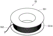
Fig. 13 is a diagram showing the coil 55 built in the communication device 2.
The coil 55 is formed in a cylindrical shape, and includes a ferrite core 551 having a groove 551A formed on an outer peripheral surface thereof and a copper wire 552 wound around the groove 551A.
When the magnetic field of the inner circumferential side of the wound copper wire 552 changes, an induced electromotive force is generated in proportion to the change, and an induced current flows through the copper wire 552 in a direction blocking the change of the magnetic field according to lenz's law.
Fig. 14 is a diagram showing magnetic fields in a case where the electronic timepiece 1 is set in the communication device 2.
As shown in fig. 14, when a pulse is output from the drive circuit 142 of the electronic timepiece 1 to the motor coil 143, a magnetic force is generated and the magnetic lines of force ML pass through the coil 55 built in the communication device 2. Thereby, the magnetic field in the coil 55 changes and an induced current flows through the copper wire 552.
[ light-emitting element ]
Fig. 15 is a diagram showing a structure of the light emitting element 56 incorporated in the lighting unit 541 of the communication device 2.
The light emitting element 56 includes a heat dissipation substrate 561 made of metal, ceramic, or the like, and 1 or more LEDs 562 provided on the heat dissipation substrate 561.
Fig. 15 (a) shows an example in which 1 LED 562 is provided, and 1 LED 562 is provided at the center of the heat dissipation substrate 561 as viewed from the front surface side (irradiation side).
Fig. 15(B) shows an example in which 3 LEDs 562 are provided, and 3 LEDs 562 are provided such that a line connecting the LEDs 562 forms a regular triangle when the heat dissipation substrate 561 is viewed from the front side.
Fig. 15(C) shows an example in which a plurality of LEDs 562 are provided, and when the heat dissipation substrate 561 is viewed from the front side, the plurality of LEDs 562 are provided in a radial pattern from the center of the heat dissipation substrate 561. In this case, light can be irradiated over a wide range.
Fig. 16 is a circuit diagram of the communication device 2, and fig. 17 is a control block diagram of the communication device 2.
As shown in fig. 16 and 17, the communication device 2 includes a control circuit 61 including a CPU, a storage device 62 including a nonvolatile memory such as a RAM or an EEPROM, a communication interface 63, an input device 64, a storage medium reading unit 65, a light-emitting element drive circuit 66, a voltage detection circuit 67, a coil 55 (receiving coil), and a light-emitting element 56.
[ Voltage detection Circuit ]
The voltage detection circuit 67 compares the induced electromotive force of the coil 55 with a predetermined threshold value to detect whether or not a current (pulse) is generated in the coil 55 by electromagnetic induction. That is, when the voltage equal to or higher than the threshold value is detected, the voltage detection circuit 67 determines that the signal has been received and outputs the determination result to the control circuit 61. Thus, as shown in fig. 17, the coil 55 and the voltage detection circuit 67 constitute an apparatus-side receiving unit 68. Here, the apparatus-side receiving unit 68 is an example of the coil receiving unit of the present invention.
[ light-emitting element drive circuit ]
The light-emitting element drive circuit 66 controls the driving of the light-emitting element 56 under the control of the control circuit 61, and transmits a "1" signal by turning on the light-emitting element 56, and transmits a "0" signal by turning off the light-emitting element 56. Accordingly, as shown in fig. 17, the light-emitting element drive circuit 66 and the light-emitting element 56 are an example of the apparatus-side transmission unit 69. Here, the device side transmission unit 69 is an example of the light transmission unit of the present invention.
The device-side transmitting unit 69 and the device-side receiving unit 68 are examples of the 2 nd communication unit according to the present invention.
[ communication interface ]
The communication interface 63 is configured to be connectable to a network such as the internet, and receives update data from the network by being connected to the network under the control of the control circuit 61. The received update data is stored in the storage device 62 by the control circuit 61.
The communication interface 63 is also connectable to an electronic device such as a PC, and is connected to the electronic device under the control of the control circuit 61 to receive update data from the electronic device. The received update data is stored in the storage device 62 by the control circuit 61.
[ input device ]
The input device 64 includes an a button 571 and a B button 572, and outputs an operation signal corresponding to the pressing operation of each button 571, 572 to the control circuit 61.
[ storage Medium reading section ]
The storage medium reading unit 65 is configured to be able to read data stored in a storage medium such as a USB (Universal Serial Bus) memory, an SD card, a CD (Compact Disc), or a DVD (Digital Versatile Disc). The storage medium reading section 65 is connected to the storage medium under the control of the control circuit 61 to read the update data from the storage data. The read update data is stored in the storage device 62 by the control circuit 61.
[ storage device ]
As shown in fig. 17, the storage device 62 includes an update data storage unit 622.
The update data storage unit 622 stores update data to be transmitted to the electronic timepiece 1. The update data may be part of or all of the system setting information 221, the reception setting information 222, the local time information 230, and the version information 223 stored in the EEPROM220 of the electronic timepiece 1.
[ control Circuit ]
The control circuit 61 functions as a device-side communication processing unit 640 by executing various programs stored in the storage device 62.
The device-side communication processing unit 640 executes a process of transmitting data (update data) from the communication device 2 to the electronic timepiece 1. The apparatus-side communication processing unit 640 includes a data request signal reception control unit 641 and a data signal transmission control unit 642.
The data request signal reception control unit 641 performs reception processing of a data request signal transmitted from the electronic timepiece 1. The data signal transmission control unit 642 performs a data signal transmission process for the electronic timepiece 1. The data signal is a signal of every 1 bit of data (update data) to be transmitted.
The details of the functional units of the control circuit 61 are described in detail in the following description of the communication process of the communication device 2.
[ communication processing of electronic timepiece ]
Fig. 18 is a flowchart showing a communication process performed by the electronic timepiece 1.
When the communication mode setting operation of the input device 160 is detected (S11), the control circuit 300 operates the timepiece-side communication processing unit 340 to set the electronic timepiece 1 to the communication mode (S12).
The clock-side communication processing unit 340 controls the drive circuit 142 of the clock-side transmission unit 180 to restrict output of a pulse different from a pulse for transmitting a signal to the motor coil 143, when operating. Specifically, the output of the needle movement pulse for instructing the time to the motor coil 143 is restricted. In addition, the timepiece-side communication processing unit 340 maintains the off state of the charge control switch 132 during operation.
First, the timepiece-side communication processing unit 340 operates the data request signal transmission control unit 341. The data request signal transmission control unit 341 controls the drive circuit 142 of the clock side transmission unit 180 to output 1 pulse, i.e., an output voltage, to the motor coil 143 and transmit a data request signal requesting acquisition of a data signal (S13).
After the data request signal transmission control unit 341 transmits the data request signal, the timepiece-side communication processing unit 340 operates the data signal reception control unit 342. The data signal reception control unit 342 controls the voltage detection circuit 133 of the clock-side reception unit 170 to detect the output voltage of the solar cell 135, and receives 1-bit data (S14).
The data signal reception control unit 342 determines whether or not the voltage detection circuit 133 has detected a voltage higher than the threshold value (S15), and when the voltage detection circuit 133 has detected a voltage higher than the threshold value (yes in S15), determines that a "1" signal has been received (S16), and outputs the reception result to the timepiece-side communication processing unit 340. On the other hand, when the voltage detection circuit 133 detects a voltage equal to or lower than the threshold value (no in S15), the data signal reception control unit 342 determines that the "0" signal is received (S17), and outputs the reception result to the timepiece-side communication processing unit 340. The data signal reception control unit 342 stores the received signal in the RAM 210.
After the data signal reception control unit 342 receives the data, the timepiece-side communication processing unit 340 determines whether or not all the update data transmitted from the communication device 2 has been received (S18). In the present embodiment, the data size, that is, the number of bits of the update data is determined in advance, and therefore, the clock-side communication processing unit 340 can determine whether or not all the update data has been received by calculating the data size (number of bits) of all the received data. The clock-side communication processing unit 340 then outputs the determination result to the control circuit 300.
If the clock-side communication processing unit 340 determines that all the update data has not been received (no in S18), the control circuit 300 determines whether or not the operation time of the clock-side communication processing unit 340 exceeds a preset data communication processing duration, that is, whether or not the operation time is a timeout (S19).
If yes is determined in S19, it can be determined that the data communication processing cannot be successfully performed, and therefore, the control circuit 300 ends the operation of the clock-side communication processing unit 340 and ends (releases) the communication mode so as not to further consume power (S20).
On the other hand, if it is determined as no in S19, the control circuit 300 returns the process to S13. Thus, the processing from S13 to S19 is repeatedly executed except when the determination at S18 is yes or the determination at S19 is yes.
If the clock-side communication processing unit 340 determines that all the update data have been received (yes in S18), the control circuit 300 writes the received data in the EEPROM220 (S21). Then, in S20, the clock-side communication processing unit 340 ends its operation, and the communication mode ends.
[ communication processing of communication apparatus ]
Fig. 19 is a flowchart showing a communication process performed by the communication apparatus 2.
Before communicating with the electronic timepiece 1, the control circuit 61 of the communication device 2 reads data to be updated from the outside using the communication interface 63 or the storage medium reading unit 65, and transmits and stores the data in the storage device 62.
When the a button 571 is pressed and a communication operation instructing the start of communication with the electronic timepiece 1 is detected, the control circuit 61 causes the device-side communication processing unit 640 to operate.
First, the device-side communication processing unit 640 operates the data request signal reception control unit 641, and the data request signal reception control unit 641 controls the voltage detection circuit 67 to detect whether or not the induced electromotive force generated in the coil 55 is equal to or greater than a threshold value, and determines whether or not the device-side reception unit 68 has received the data request signal (S31).
The data request signal reception control unit 641 continues the reception determination process S31 of the data request signal until it is determined as yes in S31.
When the data request signal reception control unit 641 determines yes in S31, the apparatus communication processing unit 640 operates the data signal transmission control unit 642, and the data signal transmission control unit 642 reads 1-bit data from the update data stored in the update data storage unit 622 (S32).
Then, the data signal transmission control unit 642 determines whether or not the read signal is a "1" signal (S33).
If it is determined as yes in S33, the data signal transmission control unit 642 controls the light-emitting element drive circuit 66 of the device-side transmission unit 69 to turn on the LED of the light-emitting element 56 and transmit a "1" signal (S34).
On the other hand, if it is determined as no in S33, the data signal transmission control unit 642 controls the light-emitting element drive circuit 66 to turn off the LED of the light-emitting element 56 and transmits a "0" signal (S35).
Next, the device-side communication processing unit 640 determines whether or not all update data has been transmitted (S36). If it is determined as no in S36, the device-side communication processing unit 640 returns the process to S31. Then, the device-side communication processing unit 640 repeatedly executes the processing from S31 to S36 until the determination in S36 is yes.
If yes is determined in S36, the control circuit 61 returns to the normal needle travel mode.
Next, the output timing of each signal when the update data is transmitted will be described.
In the timing chart of fig. 20, when the electronic timepiece 1 outputs a pulse to the motor coil 143 at time T1 and transmits a data request signal, the pulse is generated in the coil 55 of the communication device 2 by electromagnetic coupling, and the communication device 2 receives the data request signal. By receiving the data request signal, the communication device 2 controls the light emitting element driving circuit 66 to transmit the update data in units of 1 bit. In the example of fig. 20, in order to output a "1" signal as a data signal, the data signal transmission control unit 642 controls the light-emitting element drive circuit 66 to turn on the light-emitting element 56 and transmit a "1" signal.
When the light emitting element 56 is turned on, the solar cell 135 of the electronic timepiece 1 receives the light emitted from the light emitting element 56, and the output voltage of the solar cell 135 increases.
The data signal reception control unit 342 controls the voltage detection circuit 133 to detect the output voltage of the solar cell 135. The data signal reception control unit 342 transmits an operation pulse to the voltage detection circuit 133 at voltage detection timings at constant intervals, the voltage detection circuit 133 operates by the operation pulse input at the voltage detection timing of time T2, and when the output voltage of the solar cell 135 is higher than a threshold value (for example, 10,000Lx), the voltage detection circuit 133 outputs a "1" signal. In the example of fig. 20, the output voltage of the solar cell 135 exceeds the threshold value at time T2, and therefore the voltage detection circuit 133 outputs a "1" signal. Further, the determination of the received signal is determined at the falling timing of the operation pulse of the voltage detection circuit 133.
Next, when time T3, which is the transmission interval of the data request signal, arrives, the data request signal transmission control unit 341 of the electronic timepiece 1 causes the motor coil 143 to output a pulse and transmits the data request signal.
In this manner, every time a data request signal is transmitted from electronic timepiece 1 to communication device 2, the update data is transmitted from communication device 2 to electronic timepiece 1 in units of 1 bit.
After the communication process is completed, the control circuit 300 of the electronic timepiece 1 outputs a needle advance pulse to the motor coil 143, and quickly moves the hand whose driving has been stopped during the communication process to indicate the current time.
[ Effect of embodiment 1 ]
Since the communication path for transmitting a signal from electronic timepiece 1 to communication device 2 and the communication path for transmitting a signal from communication device 2 to electronic timepiece 1 are configured by 2 paths having different communication methods from each other, that is, bidirectional (full-duplex) communication is possible, the signal transmitted from electronic timepiece 1 to communication device 2 and the signal transmitted from communication device 2 to electronic timepiece 1 do not interfere with each other. Further, it is not necessary to perform switching processing such as the case of using 1 communication path by switching the transmission direction of the signal (half duplex communication), and it is also possible to simultaneously perform transmission of the signal from the electronic timepiece 1 to the communication device 2 and transmission of the signal from the communication device 2 to the electronic timepiece 1, and thus it is possible to speed up the communication processing between the electronic timepiece 1 and the communication device 2.
Further, since the communication methods of the respective communication paths are different from each other, even if the timepiece-side transmission unit 180 and the timepiece-side reception unit 170 are disposed close to each other in the electronic timepiece 1, the transmitted signal and the received signal do not interfere with each other.
In addition, since the electronic timepiece 1 transmits a signal according to whether or not a pulse is output to the motor coil 143, power consumption can be reduced compared to a case where a signal is transmitted by turning on or off a light emitting element, for example.
Since the timepiece-side receiving unit 170 is configured using the solar cell 135 for power generation provided in the electronic timepiece 1, it is not necessary to provide an additional light receiving element, and an increase in the number of components and an increase in cost can be suppressed.
Since the timepiece-side transmission unit 180 can be configured using the motor coil 143 that drives the drive mechanism provided in the electronic timepiece 1, it is not necessary to provide an additional coil, and an increase in the number of components and an increase in cost can be suppressed.
The clock-side communication processing unit 340 restricts output of a pulse different from a pulse (transmission pulse) for transmitting a signal to the motor coil 143, for example, a hand movement pulse for instructing a hand to time during operation, and therefore can suppress transmission of a signal unrelated to communication processing from the electronic timepiece 1 during communication processing. Therefore, the communication process can be performed more reliably.
Since the energy of the transmission pulse is smaller than that of the needle running pulse, the pulse width of the transmission pulse is narrower than that of the needle running pulse. In addition, when moving the hand, a plurality of needle movement pulses are required. Therefore, even if a transmission pulse is output to the motor coil 143, the hand does not move.
Since the electronic timepiece 1 receives the data signal from the communication device 2 every time the data request signal is transmitted to the communication device 2, the transmission/reception timing of the data signal can be reliably synchronized between the communication device 2 and the electronic timepiece 1. Therefore, the electronic timepiece 1 can reliably receive the data signal transmitted from the communication device 2.
When the electronic timepiece 1 is performing processing such as time counting and cannot perform signal reception processing, it is possible to control not to transmit the data signal from the communication device 2 without transmitting the data request signal. Therefore, the loss of the data signal can be prevented.
Since the data signal reception control unit 342 stores the signal received in the reception process in the EEPROM220, which is a nonvolatile memory, the signal stored in the EEPROM220 does not disappear even when the electronic timepiece 1 is reset, and it is not necessary to transmit the same signal again from the communication device 2 to the electronic timepiece 1.
For example, when a motor mounted on a timepiece is changed, it is necessary to change the waveform of a motor drive pulse for driving the motor. Therefore, it is assumed that such changed parameters and the like are generally stored in a rewritable nonvolatile memory.
The communication system 10 transmits parameters such as the speed difference rate information, the drive setting information of the stepping motor, the automatic reception interval of the satellite signal in the reception process, and the timeout time as update data from the communication device 2 to the electronic timepiece 1. This allows rewriting of various parameters stored in the EEPROM220 as a nonvolatile memory.
In addition, in recent years, the storage capacity of a nonvolatile memory has increased, and a program for operating a timepiece can be stored.
The communication system 10 transmits a program for controlling the operation of the electronic timepiece 1 as update data from the communication device 2 to the electronic timepiece 1. This allows the program stored in EEPROM220 to be rewritten.
In addition, in GPS timepieces, there is an increasing demand for updating local time information, which stores time zone information or information relating to daylight saving time, to the latest data. Therefore, the local time information is also stored in the rewritable nonvolatile memory.
When the time zone or daylight saving time is changed, the communication system 10 transmits time zone information or information related to daylight saving time as update data from the communication device 2 to the electronic timepiece 1. This allows rewriting of the local time information stored in EEPROM 220.
Since the light emitting element 56 and the coil 55 are provided in a set in the communication device 2, signals can be transmitted and received between the communication device 2 and the electronic timepiece 1 simply by placing the electronic timepiece 1 on the pedestal portion 53 of the communication device 2.
Since the light emitting element 56 of the communication device 2 is provided on the glass cover 33 side of the electronic timepiece 1 placed on the communication device 2, light emitted from the light emitting element 56 can be made incident on the solar cell 135 of the electronic timepiece 1 through the glass cover 33.
Further, since the coil 55 of the communication device 2 is provided on the back cover 34 side of the electronic timepiece 1, the coil 55 can be brought closer to the motor coil 143 of the electronic timepiece 1 than in the case where the coil is provided on the glass cover 33 side, and a signal can be transmitted from the electronic timepiece 1 to the communication device 2 more reliably.
Further, since the light emitting element 56 is continuously turned on by pressing the B button of the communication device 2, the secondary battery 130 of the electronic timepiece 1 can be charged. That is, the communication device 2 may be used as a device for charging the electronic timepiece 1.
Since the communication device 2 and the electronic timepiece 1 perform non-contact communication, when rewriting data of the EEPROM220, the operator does not need to detach the back cover of the timepiece and remove the substrate on which the nonvolatile memory is mounted from the case of the timepiece. Therefore, the operator does not need to spend the man-hour of taking out the substrate from the housing. Further, the operator does not need to remove dust or fluff that enters the case during the work, and does not need to perform a waterproof check after the back cover is closed.
Since data communication between the electronic timepiece 1 and the communication device 2 is performed according to whether or not the motor coil 143 is pulsed or whether or not the light emitting element 56 is turned on, the communication process can be simplified as compared with a case where data communication is performed by a modulated signal, for example. Therefore, the electronic timepiece 1 can reduce power consumption in the communication process.
[ 2 nd embodiment ]
The electronic timepiece of embodiment 2 is different from the electronic timepiece 1 of embodiment 1 in that the timing of writing the received data to the EEPROM220 in the communication process is different. The other structure is the same as the electronic timepiece 1.
Fig. 21 is a flowchart showing a communication process performed by the electronic timepiece of embodiment 2.
The electronic timepiece executes the processing of S11 to S20, S22, S23. The processing of S11 to S20 is the same as that of embodiment 1, and therefore, the description thereof is omitted.
In the communication processing of embodiment 2, after receiving the data signal at S16 or S17 and storing it in the RAM210, the clock-side communication processing unit 340 determines whether or not the 1 block (block) of update data transmitted from the communication device 2 has been received (S22). The 1 block is a unit of writing data to the EEPROM220, and is predetermined in accordance with the specification of the EEPROM 220. For example, 1 byte or 128 bytes, etc. may be instantiated.
If the determination at S22 is "no," the control circuit 300 returns the process to S13.
On the other hand, if yes is determined in S22, the control circuit 300 writes the received data of 1 block into the EEPROM220 (S23). Then, in S18, the timepiece-side communication processing unit 340 determines whether or not all the update data has been received. If it is determined as yes in S18, the control circuit 300 ends the operation of the clock-side communication processing unit 340 and ends the communication mode in S20.
[ Effect of embodiment 2 ]
The clock-side communication processing unit 340 writes the data stored in the RAM210 into the EEPROM220 every time it receives a data signal of 1 block which is a unit of writing into the EEPROM 220. For example, when all update data is received and stored in the RAM210 and then written into the EEPROM220, 1 block of data must be sequentially read from the update data stored in the RAM210 and written into the EEPROM220, but according to the present embodiment, such a reading process is not required and the data stored in the RAM210 may be directly written into the EEPROM220, so that the writing time for writing data into the EEPROM220 can be shortened and the power consumption of the writing process can be reduced.
[ embodiment 3 ]
The electronic timepiece 1A according to embodiment 3 is a solar-cell watch that does not have a function of receiving satellite signals from GPS satellites.
Fig. 22 is a front view of the electronic timepiece 1A, and fig. 23 is a schematic sectional view showing the electronic timepiece 1A.
As shown in fig. 22 and 23, the electronic timepiece 1A includes a case 31A to which a band 39A is attached, a glass cover 33A, and a back cover 34A. A crown 43A is provided on a side surface of the case 31A.
As shown in fig. 23, a dial ring 35A, a dial 11A, hands 21A (second hand), 22A (minute hand), 23A (hour hand), a drive mechanism 140A for driving the hands and the calendar wheel 20A, and the like are provided inside the case 31A.
A solar cell 135A is provided between the dial 11A and the bottom plate 125A to which the drive mechanism 140A is attached. In the dial 11A, the solar cell 135A, and the bottom plate 125A, holes through which the pointer shafts 29A of the pointers 21A, 22A, and 23A pass are formed, and an opening of the calendar window 15A is formed.
The driving mechanism 140A is attached to the bottom plate 125A and covered with the circuit board 120A from the back side. The drive mechanism 140A has a gear train such as a stepping motor and a gear, and the stepping motor drives each pointer and the like by rotating the pointer shaft via the gear train.
Specifically, the driving mechanism 140A includes the 1 st to 3 rd driving mechanisms. The 1 st drive mechanism drives the hands 22A and 23A, the 2 nd drive mechanism drives the hands 21A, and the 3 rd drive mechanism drives the calendar wheel 20A.
The circuit board 120A includes a control device 100A and a memory device 200A. The secondary battery 130A is provided between the bottom plate 125A and the back cover 34A.
Fig. 24 is a circuit diagram of the electronic timepiece 1A.
The electronic timepiece 1A includes a control circuit 300A, a storage device 200A, a rechargeable secondary battery 130A as a power source, a solar battery 135A, a diode 131A, a charge control switch 132A, a voltage detection circuit 133A, a motor coil 143A, and a drive circuit 142A, as in the electronic timepiece 1 of embodiment 1.
Here, the control circuit 300A, the diode 131A, the charge control switch 132A, the voltage detection circuit 133A, and the drive circuit 142A constitute the control device 100A.
The control circuit 300A does not have a function of receiving a satellite signal from a GPS satellite and a function of correcting an internal time based on position information calculated from the received satellite signal or received time information, but the other functions are the same as those of the control circuit 300 of embodiment 1. That is, the control circuit 300A includes a clock-side communication processing unit similar to the control circuit 300 of embodiment 1.
Parameters such as the speed difference rate information and the drive setting information of the stepping motor, and programs for controlling the operation of the electronic timepiece 1A are transmitted from the communication device 2 to the electronic timepiece 1A as update data.
The same operational advantages as those of embodiment 1 can be obtained in the communication system of embodiment 3.
[ other embodiments ]
The present invention is not limited to the above embodiments, and modifications, improvements, and the like are included within a range that can achieve the object of the present invention.
Fig. 25 is an external view showing a communication device 2A according to a modification of each of the above embodiments. Fig. 26 is a diagram showing the coil 55A and the light emitting element 56A in a state of being incorporated in the communication device 2A.
The communication device 2A includes a base 58, and a coil 55A and a light emitting element 56A built in the base 58. Further, a power button 573 is provided on the front surface of the pedestal portion 58.
An opening 581 is provided at the center of the pedestal portion 58 when viewed from the front side, and the light emitting element 56A is exposed through the opening 581.
As shown in fig. 25 and 26, the light emitting element 56A is provided integrally with the coil 55A. Specifically, the light emitting element 56A is provided on the inner peripheral side of the copper wire 552 wound around the coil 55A.
As shown in fig. 27, when the operator places the electronic timepiece 1 on the communication device 2A, the electronic timepiece 1 is placed so that the glass cover 33 side faces the front surface of the stand 58. At this time, when the mount 58 is viewed from the front side, the electronic timepiece 1 is mounted so that the electronic timepiece 1 overlaps the light emitting element 56A.
In the communication device 2A, magnetic lines of force generated by the motor coil 143 of the electronic timepiece 1 mainly pass through the coil 55A of the communication device 2A via the glass cover 33. Light emitted from the light emitting element 56A enters the solar cell 135 of the electronic timepiece 1 through the glass cover 33.
This enables signals to be transmitted and received between the communication device 2A and the electronic timepiece 1.
Fig. 28 is an external view showing a communication device 2B according to another modification of each of the above embodiments. Fig. 29 is a partially enlarged view of fig. 28.
The communication device 2B includes a base 58, a coil 55B built in the base 58, and a light emitting element 56B provided on the front surface of the base 58.
The coil 55B includes a rod-shaped ferrite core 553 and a copper wire 552 wound around the outer periphery of the ferrite core 553.
The coil 55B is exposed through an opening 581 of the base portion 58, and is disposed so that the axial direction of the ferrite core 553 is along the front direction of the base portion 58.
The light emitting element 56B includes a heat dissipating substrate 561B formed in a ring shape and a plurality of LEDs 562 provided along the outer periphery on the front surface of the heat dissipating substrate 561B. The light emitting element 56B is disposed such that the coil 55B is positioned on the inner peripheral side of the heat dissipating substrate 561B.
When the operator places the electronic timepiece 1 on the communication device 2B, the electronic timepiece 1 is placed so that the glass cover 33 side faces the front surface of the stand 58. At this time, when the base 58 is viewed from the front side, the electronic timepiece 1 is placed so that the electronic timepiece 1 overlaps the coil 55B.
Fig. 30 is a diagram showing magnetic fields in a case where the electronic timepiece 1 is set in the communication device 2B.
As shown in fig. 30, when a pulse is output to the motor coil 143 of the electronic timepiece 1, a magnetic force is generated and the magnetic lines of force ML pass through the coil 55B of the communication device 2B. Thus, the induced current flows through the copper wire 552 to generate a pulse.
In the communication devices 2A and 2B, light emitted from the light emitting elements 56A and 56B can be made incident on the solar cell 135 of the electronic timepiece 1 through the glass cover 33.
Further, since the coils 55A and 55B and the light emitting elements 56A and 56B are provided on the base 58, the communication devices 2A and 2B can be configured more compactly than, for example, a case where the coils 55A and 55B are provided on the base 58 and the light emitting elements 56A and 56B are provided on an arm portion extending from the base 58.
In the above embodiments, the electronic timepiece outputs a pulse to the motor coil to transmit a signal, and detects the output voltage of the solar cell to receive a signal, but the present invention is not limited to this.
For example, as shown in fig. 31, the electronic timepiece 1C may be provided with a light emitting element 136, and the electronic timepiece 1C may transmit a signal by turning on or off the light emitting element 136 and receive a signal by detecting a pulse generated in the motor coil.
In this case, the communication device 2C includes a light receiving element 59, receives a signal by detecting an output voltage of the light receiving element 59, and transmits a signal by outputting a pulse to the coil.
Fig. 32 is a front view showing an electronic timepiece 1D including a light emitting element.
The electronic timepiece 1D includes a display device 44 capable of digitally displaying time, in addition to the hands 21D (second hand), 22D (minute hand), and 23D (hour hand). The display device 44 is formed of a liquid crystal display device, an EPD (electrophoretic display), or the like.
An LED 45 for illumination is provided in the vicinity of the display device 44.
The electronic timepiece 1D has a buzzer function as an informing function, and sounds by oscillating a ceramic element attached to the back cover by a buzzer coil (booster coil) 144.
In the electronic timepiece 1D, an annular solar cell 135D is provided on the outer periphery of the dial 11D. The solar cell 135D is constituted by 4 solar cells.
The electronic timepiece 1D can transmit a signal by controlling the backlight or the LED 45 of the liquid crystal display device as a light emitting element to be turned on or off, and can receive a signal by detecting a pulse generated in the buzzer coil 144.
Alternatively, the electronic timepiece 1D can transmit a signal by outputting a pulse (transmission pulse) to the buzzer coil 144, and can receive a signal by detecting the output voltage of the solar cell 135D.
In this way, the timepiece-side transmitting portion or the timepiece-side receiving portion can be configured using the buzzer coil 144, and therefore, it is not necessary to additionally provide a coil for transmission or a coil for reception, and an increase in the number of components can be suppressed.
Since the energy of the transmission pulse is smaller than that of the emission pulse, the pulse width or voltage value of the transmission pulse is smaller than that of the emission pulse. Therefore, even if the transmission pulse is output to the buzzer coil 144, no sound is emitted. Even when the pulse width or the voltage value of the transmission pulse is the same as that of the sound emission pulse, the transmission pulse is output to the buzzer coil 144 at a low frequency of, for example, 20Hz or less, so that the buzzer sound can be made inaudible to a person.
In the electronic timepiece 1D, instead of the hands 21D, 22D, and 23D, images corresponding to the hands may be displayed on a display device 44 such as a liquid crystal display device or an EPD. In this case, the electronic timepiece 1D does not include a stepping motor, but the timepiece-side transmitting unit or the timepiece-side receiving unit can be configured using the buzzer coil 144.
In the above embodiments, the motor coil is used as the coil for transmitting a signal in the electronic timepiece, but the present invention is not limited to this. For example, the buzzer coil, a coil for driving an EL (Electro-Luminescence) lamp for illumination, or the like may be used. In the case where the electronic timepiece is a radio-controlled timepiece including an antenna for receiving a standard radio wave of a long wave, a coil of the antenna may be used as a coil for transmitting a signal.
In each of the above embodiments, the data signal transmission control unit 642 of the communication device 2 transmits the update data to the electronic timepiece 1 in units of 1 bit, but the present invention is not limited to this. For example, the update data may be transmitted in units of 2 bits or more. In this case, the data transmission rate can be made higher than in the case of transmitting in units of 1 bit.
In each of the above embodiments, the data signal transmission control unit 642 reads the update data stored in the update data storage unit 622, but the present invention is not limited to this. For example, the data signal transmission control unit 642 may control the storage medium reading unit 65 to read the update data stored in the storage medium, or may control the communication interface 63 to read the update data stored in an electronic device such as a PC or the like or the update data on the network.
In each of the above embodiments, the data signal transmission control unit 642 of the communication device 2 controls the light emitting element drive circuit 66 of the device side transmission unit 69 to turn on or off the light emitting element 56 and transmit the "1" signal or the "0" signal, but the present invention is not limited thereto. For example, the luminance of the light-emitting element may be adjusted to transmit a "1" signal or a "0" signal.
In each of the above embodiments, the clock-side receiving unit 170 includes the solar cell 135 as the light receiving element, but the present invention is not limited thereto. That is, a light receiving element other than the solar cell, such as a light receiving element for light detection, may be provided.
In each of the above embodiments, the clock side receiving unit 170 detects the output voltage of the solar cell 135 to receive a signal, but the present invention is not limited thereto. For example, the signal may be received by detecting the output current of the solar cell 135.
The device-side receiving unit 68 receives a signal by detecting the voltage of the coil 55, but the present invention is not limited to this. For example, the signal may be received by detecting the current of the coil 55.
In the above-described embodiments 1 and 2, the timepiece-side communication processing part 340 may restrict the operations of the time part 310 and the positioning part 320 when operating. Accordingly, the satellite signal reception processing can be restricted from being executed in the communication processing, and the influence of the satellite signal reception processing on the communication processing can be suppressed.
In the above embodiments, data is transmitted from the communication device 2 to the electronic timepiece 1, but the present invention is not limited to this. For example, in the manufacturing process of the electronic timepiece 1, data may be transmitted from the communication device 2 to the movement before being assembled to the case.
Accordingly, it is not necessary to provide a terminal for data writing in the movement and connect the terminal to a dedicated jig to write data, and therefore, it is not necessary to perform alignment between the terminal and the jig, and the data writing operation can be simplified, and the manufacturing process can be simplified.
Claims (21)
1. A communication system having an electronic clock and a communication device, the communication system being characterized in that,
one of the electronic timepiece and the communication device includes a 1 st communication unit,
the other of the electronic timepiece and the communication device includes a 2 nd communication unit capable of communicating with the 1 st communication unit,
the 1 st communication unit includes:
a coil transmission unit that includes a transmission coil and a drive circuit that drives the transmission coil, and that transmits a signal by electromagnetic coupling-based communication using the transmission coil; and
a light receiving unit which is provided with a light receiving element and a detection circuit for detecting an output value of the light receiving element and receives a signal by optical communication using the light receiving element,
the 2 nd communication unit includes:
a light transmission unit that includes a light emitting element and a drive circuit that drives the light emitting element, and transmits a signal by light-based communication using the light emitting element; and
a coil receiving unit which is provided with a receiving coil and a detection circuit for detecting an output value of the receiving coil, and which receives a signal by communication based on electromagnetic coupling using the receiving coil,
the light-based communication and the electromagnetic coupling-based communication are each unidirectional communication.
2. An electronic timepiece is characterized by comprising:
a coil transmission unit that includes a transmission coil and a drive circuit that drives the transmission coil, and that transmits a signal by electromagnetic coupling-based communication using the transmission coil; and
a light receiving unit which is provided with a light receiving element and a detection circuit for detecting an output value of the light receiving element and receives a signal by optical communication using the light receiving element,
the light-based communication and the electromagnetic coupling-based communication are each unidirectional communication.
3. Electronic timepiece according to claim 2,
the electronic timepiece includes a solar cell that receives light and generates electricity,
the light receiving element is formed of the solar cell.
4. Electronic timepiece according to claim 2 or 3,
the electronic timepiece includes a motor that drives a driven member,
the transmission coil is formed of a motor coil provided in the motor.
5. Electronic timepiece according to claim 2 or 3,
the electronic timepiece is provided with a buzzer for informing,
the transmission coil is constituted by a buzzer coil provided in the buzzer.
6. Electronic timepiece according to claim 2 or 3,
the electronic timepiece includes a timepiece-side communication processing unit that controls the coil transmission unit and the light receiving unit to perform communication processing,
when performing communication processing, the timepiece-side communication processing unit restricts output of a pulse different from a pulse for transmitting a signal to the transmission coil.
7. Electronic timepiece according to claim 2 or 3,
the electronic timepiece includes:
a clock side transmission control unit that controls the coil transmission unit and performs transmission processing of a data request signal for requesting a communication device to acquire a data signal; and
and a clock-side reception control unit that controls the light receiving unit and performs reception processing of the data signal transmitted from the communication device.
8. Electronic timepiece according to claim 2 or 3,
the electronic timepiece includes a nonvolatile memory for storing a signal,
the signal received by the light receiving section is stored in the nonvolatile memory.
9. Electronic timepiece according to claim 2 or 3,
the signal received by the light receiving unit includes a signal of a parameter for controlling the operation of the electronic timepiece.
10. Electronic timepiece according to claim 2 or 3,
the signal received by the light receiving unit includes a signal of a program for controlling the operation of the electronic timepiece.
11. Electronic timepiece according to claim 2 or 3,
the signal received by the light receiving unit includes time zone information or information related to daylight saving time.
12. An electronic timepiece is characterized by comprising:
a light transmission unit that includes a light emitting element and a drive circuit that drives the light emitting element, and transmits a signal by light-based communication using the light emitting element; and
a coil receiving unit which is provided with a receiving coil and a detection circuit for detecting an output value of the receiving coil, and which receives a signal by communication based on electromagnetic coupling using the receiving coil,
the light-based communication and the electromagnetic coupling-based communication are each unidirectional communication.
13. Electronic timepiece according to claim 12,
the electronic timepiece includes:
a clock-side transmission control unit that controls the optical transmission unit and performs transmission processing of a data request signal for requesting a communication device to acquire a data signal; and
and a timepiece-side reception control unit that controls the coil reception unit and performs reception processing of the data signal transmitted from the communication device.
14. Electronic timepiece according to claim 12 or 13,
the electronic timepiece includes a nonvolatile memory for storing a signal,
the signal received by the coil receiving section is stored in the nonvolatile memory.
15. Electronic timepiece according to claim 12 or 13,
the signal received by the coil receiving unit includes a signal for controlling a parameter of the operation of the electronic timepiece.
16. Electronic timepiece according to claim 12 or 13,
the signal received by the coil receiving unit includes a signal of a program for controlling the operation of the electronic timepiece.
17. Electronic timepiece according to claim 12 or 13,
the signal received by the coil receiving unit includes time zone information or information related to daylight saving time.
18. A communication device is characterized by comprising:
a light transmission unit that includes a light emitting element and a drive circuit that drives the light emitting element, and transmits a signal by light-based communication using the light emitting element; and
a coil receiving unit which is provided with a receiving coil and a detection circuit for detecting an output value of the receiving coil, and which receives a signal by communication based on electromagnetic coupling using the receiving coil,
the light-based communication and the electromagnetic coupling-based communication are each unidirectional communication.
19. The communication device of claim 18,
the communication device includes a mounting portion for mounting an electronic timepiece,
the receiving coil is provided on the back cover side of the electronic timepiece placed on the placement unit,
the light emitting element is provided on the glass cover side of the electronic timepiece placed on the placement portion.
20. The communication device of claim 18,
the communication device includes a mounting portion for mounting an electronic timepiece,
the receiving coil and the light emitting element are provided on a glass cover side of the electronic timepiece placed on the placement portion.
21. A communication device is characterized by comprising:
a coil transmission unit that includes a transmission coil and a drive circuit that drives the transmission coil, and that transmits a signal by electromagnetic coupling-based communication using the transmission coil; and
a light receiving unit which is provided with a light receiving element and a detection circuit for detecting an output value of the light receiving element and receives a signal by optical communication using the light receiving element,
the light-based communication and the electromagnetic coupling-based communication are each unidirectional communication.
Applications Claiming Priority (2)
| Application Number | Priority Date | Filing Date | Title |
|---|---|---|---|
| JP2015081096A JP6547379B2 (en) | 2015-04-10 | 2015-04-10 | Communication system, electronic watch and communication device |
| JP2015-081096 | 2015-04-10 |
Publications (2)
| Publication Number | Publication Date |
|---|---|
| CN106054588A CN106054588A (en) | 2016-10-26 |
| CN106054588B true CN106054588B (en) | 2020-03-27 |
Family
ID=55701838
Family Applications (1)
| Application Number | Title | Priority Date | Filing Date |
|---|---|---|---|
| CN201610185038.XA Active CN106054588B (en) | 2015-04-10 | 2016-03-29 | Communication system, electronic timepiece, and communication device |
Country Status (4)
| Country | Link |
|---|---|
| US (1) | US10009116B2 (en) |
| EP (1) | EP3079025A1 (en) |
| JP (1) | JP6547379B2 (en) |
| CN (1) | CN106054588B (en) |
Families Citing this family (13)
| Publication number | Priority date | Publication date | Assignee | Title |
|---|---|---|---|---|
| KR102595232B1 (en) * | 2016-09-23 | 2023-10-30 | 삼성전자주식회사 | Wireless power transmission apparatus in electronic device and method thereof |
| EP3318933B1 (en) * | 2016-11-02 | 2020-03-25 | Montres Breguet S.A. | Device for immobilising and/or winding a marine chronometer |
| EP3379347B1 (en) * | 2017-03-20 | 2020-01-01 | ETA SA Manufacture Horlogère Suisse | Method for adjusting the operation frequency of an electronic watch |
| EP3396871A1 (en) * | 2017-04-25 | 2018-10-31 | ETA SA Manufacture Horlogère Suisse | Method for transmitting data from an electronic apparatus to an electronic device |
| EP3379346B1 (en) * | 2017-03-20 | 2022-08-03 | ETA SA Manufacture Horlogère Suisse | Method for adjusting a quartz watch |
| CN110462529B (en) * | 2017-03-29 | 2021-06-29 | 西铁城时计株式会社 | Analog electronic timepiece system and analog electronic timepiece |
| EP3413146B1 (en) * | 2017-06-06 | 2019-11-27 | EM Microelectronic-Marin SA | Electronic device for receiving data |
| JP7279824B2 (en) * | 2017-09-04 | 2023-05-23 | カシオ計算機株式会社 | ELECTRONIC CLOCK, REGION DETERMINATION METHOD, AND PROGRAM |
| EP3502799A1 (en) * | 2017-12-22 | 2019-06-26 | The Swatch Group Research and Development Ltd | Device for recharging an electromechanical or electronic watch and assembly comprising same |
| US20200044468A1 (en) * | 2018-07-31 | 2020-02-06 | Ling Yung LIN | Mobile power supply module with light source |
| EP3627243B1 (en) | 2018-09-20 | 2021-05-12 | ETA SA Manufacture Horlogère Suisse | Method for adjusting the average frequency of a time base incorporated in an electronic watch |
| JP7143708B2 (en) * | 2018-09-28 | 2022-09-29 | セイコーエプソン株式会社 | electronic clock |
| CH717687A1 (en) * | 2020-07-27 | 2022-01-31 | Metallo Tests Sa | System and method for checking timepieces and electronic measurement module. |
Citations (4)
| Publication number | Priority date | Publication date | Assignee | Title |
|---|---|---|---|---|
| US4800543A (en) * | 1987-12-03 | 1989-01-24 | Ramtron Corporation | Timepiece communication system |
| US5978656A (en) * | 1995-12-28 | 1999-11-02 | Asulab S.A. | Portable device using inductive antenna to receive data transmitted via modulating vertical or horizonal line synchronization signals of a swept frame video display monitor |
| JP2001099964A (en) * | 1999-09-30 | 2001-04-13 | Seiko Epson Corp | Electronic watch and control method of electronic watch |
| JP2006349499A (en) * | 2005-06-16 | 2006-12-28 | Citizen Watch Co Ltd | Charging device |
Family Cites Families (18)
| Publication number | Priority date | Publication date | Assignee | Title |
|---|---|---|---|---|
| JPS5487264A (en) * | 1977-12-22 | 1979-07-11 | Seiko Instr & Electronics Ltd | Electronic watch |
| CH639236GA3 (en) * | 1980-05-21 | 1983-11-15 | Electronic timepiece including an information reception device | |
| JP3674443B2 (en) * | 1999-03-11 | 2005-07-20 | セイコーエプソン株式会社 | Electronic device, external adjustment device for electronic device, control method for electronic device, and control method for external adjustment device |
| CN1236367C (en) | 1999-07-16 | 2006-01-11 | 时至准钟表股份有限公司 | Time piece |
| US6850468B2 (en) * | 1999-09-17 | 2005-02-01 | Seiko Epson Corporation | Electronic timepiece, control method for electronic timepiece, regulating system for electronic timepiece, and regulating method for electronic timepiece |
| DE60123403T2 (en) * | 2000-08-11 | 2007-08-23 | Seiko Epson Corp. | ELECTRONIC DEVICE AND METHOD FOR CONTROLLING THEREOF |
| EP1553469A4 (en) * | 2003-07-04 | 2005-08-10 | Seiko Epson Corp | Time correction system, time correction designating unit, pointer type clock, and method for correcting time |
| JP2005241403A (en) | 2004-02-26 | 2005-09-08 | Citizen Watch Co Ltd | Auxiliary antenna system of radio-controlled watch, and the radio-controlled watch |
| JP2006105826A (en) | 2004-10-06 | 2006-04-20 | Torigaa:Kk | Electronic wrist watch |
| KR100724879B1 (en) * | 2006-03-06 | 2007-06-04 | 삼성전자주식회사 | Method for updating daylight saving time in wireless terminal |
| JP2012173021A (en) * | 2011-02-18 | 2012-09-10 | Casio Comput Co Ltd | Electronic timepiece |
| JP2014048136A (en) | 2012-08-30 | 2014-03-17 | Seiko Precision Inc | Time correction system, time transmission device, time correction device, time correction method, and program |
| JP2014053657A (en) | 2012-09-05 | 2014-03-20 | Casio Comput Co Ltd | Data input device and data input method |
| US10067480B2 (en) * | 2013-11-12 | 2018-09-04 | Seiko Instruments Inc. | Time correction system, electronic device, timepiece, and program |
| US9709962B2 (en) * | 2013-11-12 | 2017-07-18 | Seiko Instruments Inc. | Time correction system, electronic device, timepiece, and program |
| US10228660B2 (en) * | 2014-03-03 | 2019-03-12 | Seiko Instruments Inc. | Electronic apparatus and control method |
| GB2524523B (en) * | 2014-03-25 | 2016-09-14 | Sciteb Ltd | Watches for use in time-dependent authentication systems, and methods of use thereof in authentication protocols |
| JP6202017B2 (en) * | 2015-02-24 | 2017-09-27 | カシオ計算機株式会社 | Electronic timepiece, communication system and program |
-
2015
- 2015-04-10 JP JP2015081096A patent/JP6547379B2/en active Active
-
2016
- 2016-03-29 CN CN201610185038.XA patent/CN106054588B/en active Active
- 2016-04-08 EP EP16164423.2A patent/EP3079025A1/en not_active Withdrawn
- 2016-04-08 US US15/094,366 patent/US10009116B2/en active Active
Patent Citations (4)
| Publication number | Priority date | Publication date | Assignee | Title |
|---|---|---|---|---|
| US4800543A (en) * | 1987-12-03 | 1989-01-24 | Ramtron Corporation | Timepiece communication system |
| US5978656A (en) * | 1995-12-28 | 1999-11-02 | Asulab S.A. | Portable device using inductive antenna to receive data transmitted via modulating vertical or horizonal line synchronization signals of a swept frame video display monitor |
| JP2001099964A (en) * | 1999-09-30 | 2001-04-13 | Seiko Epson Corp | Electronic watch and control method of electronic watch |
| JP2006349499A (en) * | 2005-06-16 | 2006-12-28 | Citizen Watch Co Ltd | Charging device |
Also Published As
| Publication number | Publication date |
|---|---|
| JP6547379B2 (en) | 2019-07-24 |
| JP2016200508A (en) | 2016-12-01 |
| EP3079025A1 (en) | 2016-10-12 |
| CN106054588A (en) | 2016-10-26 |
| US20160299475A1 (en) | 2016-10-13 |
| US10009116B2 (en) | 2018-06-26 |
Similar Documents
| Publication | Publication Date | Title |
|---|---|---|
| CN106054588B (en) | Communication system, electronic timepiece, and communication device | |
| CN106168752B (en) | Electronic timepiece, communication device, and communication system | |
| US10691076B2 (en) | Electronic timepiece | |
| US20140247700A1 (en) | Electronic Timepiece and Time Correction Method of Electronic Timepiece | |
| US20140241131A1 (en) | Electronic Timepiece | |
| JP6354289B2 (en) | Radio wave receiving apparatus, electronic device, and radio wave receiving method | |
| JP7010355B2 (en) | Electronic clock | |
| CN105938322B (en) | Electronic device and control method of electronic device | |
| JP2018119925A (en) | Electronic watch | |
| JP2018194310A (en) | Electronic timepiece and method for controlling electronic timepiece | |
| JP6471425B2 (en) | Communication device, electronic timepiece, and communication device control method | |
| JP2019158343A (en) | Electronic watch | |
| JP6759597B2 (en) | Electronic clock and control method of electronic clock | |
| JP6102328B2 (en) | Electronics | |
| JP2016200509A (en) | Communication system, electronic timekeeper, communication device, and method for controlling electronic timekeeper | |
| JP6733380B2 (en) | Electronic timepiece and electronic timepiece control method | |
| US10571867B2 (en) | Electronic timepiece | |
| CN110308646B (en) | Electronic clock | |
| JP7176207B2 (en) | Electronic devices and methods of controlling electronic devices | |
| JP2017138160A (en) | Electronic apparatus and control method of the same | |
| JP2017129551A (en) | Electronic apparatus, and control method for the same | |
| JP2017173042A (en) | Electronic apparatus and control method for the same | |
| JP2017032464A (en) | Electronic timepiece | |
| JP2022187760A (en) | Time radio wave transmitter and time measuring system | |
| JP2019164101A (en) | Electronic watch |
Legal Events
| Date | Code | Title | Description |
|---|---|---|---|
| C06 | Publication | ||
| PB01 | Publication | ||
| SE01 | Entry into force of request for substantive examination | ||
| SE01 | Entry into force of request for substantive examination | ||
| GR01 | Patent grant | ||
| GR01 | Patent grant |