CN105452981B - Display device - Google Patents
Display device Download PDFInfo
- Publication number
- CN105452981B CN105452981B CN201480043745.4A CN201480043745A CN105452981B CN 105452981 B CN105452981 B CN 105452981B CN 201480043745 A CN201480043745 A CN 201480043745A CN 105452981 B CN105452981 B CN 105452981B
- Authority
- CN
- China
- Prior art keywords
- region
- display
- display device
- image
- film
- Prior art date
- Legal status (The legal status is an assumption and is not a legal conclusion. Google has not performed a legal analysis and makes no representation as to the accuracy of the status listed.)
- Active
Links
Images


Classifications
-
- G—PHYSICS
- G09—EDUCATION; CRYPTOGRAPHY; DISPLAY; ADVERTISING; SEALS
- G09G—ARRANGEMENTS OR CIRCUITS FOR CONTROL OF INDICATING DEVICES USING STATIC MEANS TO PRESENT VARIABLE INFORMATION
- G09G3/00—Control arrangements or circuits, of interest only in connection with visual indicators other than cathode-ray tubes
- G09G3/20—Control arrangements or circuits, of interest only in connection with visual indicators other than cathode-ray tubes for presentation of an assembly of a number of characters, e.g. a page, by composing the assembly by combination of individual elements arranged in a matrix no fixed position being assigned to or needed to be assigned to the individual characters or partial characters
-
- G—PHYSICS
- G06—COMPUTING; CALCULATING OR COUNTING
- G06F—ELECTRIC DIGITAL DATA PROCESSING
- G06F1/00—Details not covered by groups G06F3/00 - G06F13/00 and G06F21/00
- G06F1/16—Constructional details or arrangements
- G06F1/1613—Constructional details or arrangements for portable computers
- G06F1/1633—Constructional details or arrangements of portable computers not specific to the type of enclosures covered by groups G06F1/1615 - G06F1/1626
- G06F1/1637—Details related to the display arrangement, including those related to the mounting of the display in the housing
- G06F1/1652—Details related to the display arrangement, including those related to the mounting of the display in the housing the display being flexible, e.g. mimicking a sheet of paper, or rollable
-
- G—PHYSICS
- G06—COMPUTING; CALCULATING OR COUNTING
- G06F—ELECTRIC DIGITAL DATA PROCESSING
- G06F3/00—Input arrangements for transferring data to be processed into a form capable of being handled by the computer; Output arrangements for transferring data from processing unit to output unit, e.g. interface arrangements
- G06F3/01—Input arrangements or combined input and output arrangements for interaction between user and computer
- G06F3/03—Arrangements for converting the position or the displacement of a member into a coded form
- G06F3/041—Digitisers, e.g. for touch screens or touch pads, characterised by the transducing means
- G06F3/0412—Digitisers structurally integrated in a display
-
- G—PHYSICS
- G06—COMPUTING; CALCULATING OR COUNTING
- G06F—ELECTRIC DIGITAL DATA PROCESSING
- G06F3/00—Input arrangements for transferring data to be processed into a form capable of being handled by the computer; Output arrangements for transferring data from processing unit to output unit, e.g. interface arrangements
- G06F3/01—Input arrangements or combined input and output arrangements for interaction between user and computer
- G06F3/03—Arrangements for converting the position or the displacement of a member into a coded form
- G06F3/041—Digitisers, e.g. for touch screens or touch pads, characterised by the transducing means
- G06F3/0414—Digitisers, e.g. for touch screens or touch pads, characterised by the transducing means using force sensing means to determine a position
- G06F3/04146—Digitisers, e.g. for touch screens or touch pads, characterised by the transducing means using force sensing means to determine a position using pressure sensitive conductive elements delivering a boolean signal and located between crossing sensing lines, e.g. located between X and Y sensing line layers
-
- G—PHYSICS
- G09—EDUCATION; CRYPTOGRAPHY; DISPLAY; ADVERTISING; SEALS
- G09F—DISPLAYING; ADVERTISING; SIGNS; LABELS OR NAME-PLATES; SEALS
- G09F9/00—Indicating arrangements for variable information in which the information is built-up on a support by selection or combination of individual elements
- G09F9/30—Indicating arrangements for variable information in which the information is built-up on a support by selection or combination of individual elements in which the desired character or characters are formed by combining individual elements
- G09F9/301—Indicating arrangements for variable information in which the information is built-up on a support by selection or combination of individual elements in which the desired character or characters are formed by combining individual elements flexible foldable or roll-able electronic displays, e.g. thin LCD, OLED
-
- H—ELECTRICITY
- H10—SEMICONDUCTOR DEVICES; ELECTRIC SOLID-STATE DEVICES NOT OTHERWISE PROVIDED FOR
- H10K—ORGANIC ELECTRIC SOLID-STATE DEVICES
- H10K77/00—Constructional details of devices covered by this subclass and not covered by groups H10K10/80, H10K30/80, H10K50/80 or H10K59/80
- H10K77/10—Substrates, e.g. flexible substrates
- H10K77/111—Flexible substrates
-
- G—PHYSICS
- G06—COMPUTING; CALCULATING OR COUNTING
- G06F—ELECTRIC DIGITAL DATA PROCESSING
- G06F2203/00—Indexing scheme relating to G06F3/00 - G06F3/048
- G06F2203/041—Indexing scheme relating to G06F3/041 - G06F3/045
- G06F2203/04102—Flexible digitiser, i.e. constructional details for allowing the whole digitising part of a device to be flexed or rolled like a sheet of paper
-
- G—PHYSICS
- G06—COMPUTING; CALCULATING OR COUNTING
- G06F—ELECTRIC DIGITAL DATA PROCESSING
- G06F3/00—Input arrangements for transferring data to be processed into a form capable of being handled by the computer; Output arrangements for transferring data from processing unit to output unit, e.g. interface arrangements
- G06F3/01—Input arrangements or combined input and output arrangements for interaction between user and computer
- G06F3/03—Arrangements for converting the position or the displacement of a member into a coded form
- G06F3/041—Digitisers, e.g. for touch screens or touch pads, characterised by the transducing means
- G06F3/044—Digitisers, e.g. for touch screens or touch pads, characterised by the transducing means by capacitive means
- G06F3/0446—Digitisers, e.g. for touch screens or touch pads, characterised by the transducing means by capacitive means using a grid-like structure of electrodes in at least two directions, e.g. using row and column electrodes
-
- G—PHYSICS
- G09—EDUCATION; CRYPTOGRAPHY; DISPLAY; ADVERTISING; SEALS
- G09G—ARRANGEMENTS OR CIRCUITS FOR CONTROL OF INDICATING DEVICES USING STATIC MEANS TO PRESENT VARIABLE INFORMATION
- G09G2310/00—Command of the display device
- G09G2310/02—Addressing, scanning or driving the display screen or processing steps related thereto
- G09G2310/0262—The addressing of the pixel, in a display other than an active matrix LCD, involving the control of two or more scan electrodes or two or more data electrodes, e.g. pixel voltage dependent on signals of two data electrodes
-
- G—PHYSICS
- G09—EDUCATION; CRYPTOGRAPHY; DISPLAY; ADVERTISING; SEALS
- G09G—ARRANGEMENTS OR CIRCUITS FOR CONTROL OF INDICATING DEVICES USING STATIC MEANS TO PRESENT VARIABLE INFORMATION
- G09G2330/00—Aspects of power supply; Aspects of display protection and defect management
- G09G2330/02—Details of power systems and of start or stop of display operation
- G09G2330/021—Power management, e.g. power saving
-
- H—ELECTRICITY
- H10—SEMICONDUCTOR DEVICES; ELECTRIC SOLID-STATE DEVICES NOT OTHERWISE PROVIDED FOR
- H10K—ORGANIC ELECTRIC SOLID-STATE DEVICES
- H10K2102/00—Constructional details relating to the organic devices covered by this subclass
- H10K2102/301—Details of OLEDs
- H10K2102/311—Flexible OLED
Landscapes
- Engineering & Computer Science (AREA)
- Theoretical Computer Science (AREA)
- General Engineering & Computer Science (AREA)
- Physics & Mathematics (AREA)
- General Physics & Mathematics (AREA)
- Computer Hardware Design (AREA)
- Human Computer Interaction (AREA)
- Control Of Indicators Other Than Cathode Ray Tubes (AREA)
- Electroluminescent Light Sources (AREA)
- Devices For Indicating Variable Information By Combining Individual Elements (AREA)
- Control Of El Displays (AREA)
- Controls And Circuits For Display Device (AREA)
- Chemical & Material Sciences (AREA)
- Crystallography & Structural Chemistry (AREA)
- User Interface Of Digital Computer (AREA)
- Thin Film Transistor (AREA)
- Power Sources (AREA)
Abstract
A display device with low power consumption is provided. Further, a display device that displays an image in a region that can be used in a folded state is provided. The display device includes a display unit that can be unfolded and folded, a detection unit that detects the folded state, and an image processing unit that generates an image in which a black image is displayed on a part of the display unit when the display unit is in the folded state.
Description
Technical Field
The present invention relates to an object, a method or a method of manufacture. Furthermore, the present invention relates to a process (process), machine (machine), product (manufacture) or composition (matter). In particular, the present invention relates to a human-machine interface, a semiconductor device, a display device, a light-emitting device, a power storage device, a method for driving the same, or a method for manufacturing the same, for example. For example, the present invention particularly relates to a display device. In particular, one embodiment of the present invention relates to a foldable display device.
Background
The social base associated with information transfer methods is becoming more and more substantial. By using an information processor, a wide variety of information can be obtained, processed, or transmitted not only at home or at work but also at home or at home.
In the background described above, development of portable information processors has been actively conducted.
For example, portable information processors are often used outdoors, and sometimes the portable information processors and display devices contained therein are subjected to unexpected external forces by being dropped. As an example of a display device which is not easily broken, a display device in which the adhesion between a structure in which light-emitting layers are separated and a second electrode layer is high is known (patent document 1).
Multi-panel electronic devices having the following functions are known. First acceleration data is received from a first sensor coupled to a first portion of an electronic device. Additionally, second acceleration data is also received from a second sensor coupled to a second portion of the electronic device, and a position of the first portion is movable relative to a position of the second portion. Further, the configuration of the electronic device is determined based on at least a part of the first acceleration data and a part of the second acceleration data (patent document 2).
[ reference documents ]
[ patent document ]
[ patent document 1] Japanese patent application laid-open No. 2012-190794
[ patent document 2] Japanese patent application laid-open No. 2012-502372
Disclosure of Invention
An object of one embodiment of the present invention is to provide a display device with low power consumption. Another object is to provide a display device that displays an image in an area that can be used in a folded state. Another object is to provide a novel display device.
Note that the description of these objects does not hinder the existence of other objects. In one embodiment of the present invention, not all of the above objects need be achieved. Other objects are apparent from and can be extracted from the description of the specification, the drawings, the claims, and the like.
One embodiment of the present invention is a display device including: a foldable display unit having a first region and a second region; a detection part for detecting the unfolding state or folding state of the display part and supplying a folding signal; a control part for receiving the folding signal and supplying an image control signal; an image processing unit for receiving an image control signal, generating an image signal, and supplying the image signal; and a drive circuit for receiving the image signal and driving the display unit. The control section supplies an image control signal for causing the image processing section to generate an image in which a black image is displayed in the second region of the display section in a folded state.
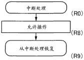
Another aspect of the present invention is the display device described above, wherein the control portion has an arithmetic unit and a storage unit that stores a program executed by the arithmetic unit. The program includes a first step of allowing interrupt processing; a third step of entering when the display portion is in the unfolded state, and a second step of entering the fourth step when the display portion is in the folded state; a third step of generating an image displayed in the first area and the second area; a fourth step of generating an image in which a black image is displayed in the second region; a fifth step of displaying an image on the display section; when an end instruction is supplied in the interrupt processing, the seventh step is entered, and when an end instruction is not supplied, the sixth step of the second step is returned to; and a seventh step of ending the routine. The interrupt processing includes an eighth step of allowing the operation and a ninth step of recovering from the interrupt processing.
The display device according to one aspect of the present invention includes a display unit that can be unfolded and folded, a detection unit that detects a folded state of the display unit, and an image processing unit that generates an image in which a black image is displayed on a part of the display unit when the display unit is in the folded state. Thus, a region which is not required to be displayed when a part of the display portion is folded can display a black image. As a result, a display device with low power consumption can be provided. Further, a display device that displays an image in a region that can be used in a folded state can be provided.
Another embodiment of the present invention is a display device including: a foldable display unit having a first region and a second region; a detection part for detecting the unfolding state or folding state of the display part and supplying a folding signal; a control part for receiving the folding signal and supplying the image control signal and the synchronous control signal; an image processing unit for receiving the image control signal, generating a first image signal and a second image signal, and supplying the signals; a synchronous signal supply part for receiving the synchronous control signal and supplying a first synchronous signal and a second synchronous signal; a first driving circuit for receiving a first image signal and a first synchronization signal to drive the first region; and a second driving circuit for receiving the second image signal and the second synchronous signal to drive the second region. The control section supplies an image control signal for causing the image processing section to generate an image for displaying a black image in the second region of the display section in the folded state and a synchronization control signal for stopping selection of the scanning line in the second region of the display section in the folded state.
Another aspect of the present invention is the display device described above, wherein the control portion has an arithmetic unit and a storage unit that stores a program executed by the arithmetic unit. The program includes a first step of allowing interrupt processing; a third step of entering when the display portion is in the unfolded state, and a second step of entering the fourth step when the display portion is in the folded state; entering a fifth step when the unfolded state is not changed, and entering a third step of a sixth step when the unfolded state is changed into the folded state; entering a seventh step when the folded state is not changed, and entering a fourth step of the eighth step when the folded state is changed to the unfolded state; a fifth step of performing process 1; a sixth step of performing process 2; the seventh step of the process 3 is executed; an eighth step of performing process 4; entering the tenth step when an end instruction is supplied in the interrupt processing, and returning to the ninth step of the second step when an end instruction is not supplied; and a tenth step of ending the routine. The interrupt processing includes an eleventh step of allowing an operation and a twelfth step of resuming from the interrupt processing.
Another embodiment of the present invention is the display device described above, wherein the program has four kinds of processing as follows. The process 1 includes a first step of causing the synchronization signal supply section to supply the synchronization signal to the first drive circuit and the second drive circuit; a second step of causing the image processing unit to generate an image to be displayed in the first region and the second region; a third step of displaying an image on the display unit; and a fourth step of recovering from process 1. The process 2 includes a first step of causing the synchronization signal supply section to supply the synchronization signal to the first drive circuit and the second drive circuit; a second step of causing the image processing unit to generate an image of a black image displayed in the second region; a third step of displaying an image on the display unit; a fourth step of sequentially stopping the synchronous signal supply section from supplying the synchronous signal to the second drive circuit; and a fifth step of recovering from the process 2. The process 3 includes a first step of causing the synchronization signal supply section to supply the synchronization signal to the first drive circuit; a second step of causing the image processing unit to generate an image to be displayed in the first region; a third step of causing the display section to display an image in the first region; and a fourth step of recovering from the process 3. The process 4 includes a first step of causing the synchronization signal supply section to sequentially supply the synchronization signals to the second drive circuit; a second step of causing the image processing unit to generate an image to be displayed in the first region and the second region; a third step of displaying an image on the display unit; and a fourth step of recovering from the process 4.
The display device according to one aspect of the present invention includes a display unit that can be unfolded and folded, a detection unit that detects a folded state of the display unit, an image processing unit that generates an image in which a black image is displayed on a part of the display unit when the display unit is in the folded state, and a synchronization signal supply unit that can stop supply of a synchronization signal for the part in which the black image is displayed. Thereby, the display in the region where the display is unnecessary when a part of the display portion is folded can be stopped. As a result, a display device with low power consumption can be provided. In addition, a display device that displays an image in a region that can be used in a folded state can be provided.
Another aspect of the present invention is the display device described above, further including a first power supply which supplies a power supply potential to the first drive circuit, and a second power supply which supplies a power supply potential to the second drive circuit. The control part supplies a power control signal to the second power supply according to the folding signal. The second power supply stops the supply of the power supply potential according to the power supply control signal.
The display device according to one aspect of the present invention includes a display unit that can be unfolded and folded, a synchronization signal supply unit that can stop supply of a synchronization signal to a portion where a black image is displayed, and a power supply that can stop supply of a power supply potential to the portion where the black image is displayed. Thereby, the display in the region where the display is unnecessary when a part of the display portion is folded can be stopped. As a result, a display device with low power consumption can be provided. In addition, a display device that displays an image in a region that can be used in a folded state can be provided.
Another aspect of the present invention is the display device described above, further comprising a magnet, wherein the detection unit includes a magnetic sensor. The magnet is disposed at a position where the magnetic sensor can detect the unfolded state or the folded state of the display unit.
The display device according to one aspect of the present invention includes a display unit that can be unfolded and folded, a magnet that is disposed to detect a folded state of the display unit, a detection unit that includes a magnetic sensor, and an image processing unit that generates an image in which a black image is displayed on a part of the display unit when the display unit is in the folded state. Thus, a region which is not required to be displayed when a part of the display portion is folded can display a black image. Further, the folded state may be maintained using the magnetic force of the magnet. As a result, a display device with low power consumption can be provided. In addition, a display device that displays an image in a region that can be used in a folded state can be provided.
According to one embodiment of the present invention, a display device with low power consumption can be provided. In addition, a display device that displays an image in a region that can be used in a folded state can be provided.
Drawings
Fig. 1A, 1B1, and 1B2 are a block diagram and a schematic diagram illustrating a structure of a display device according to an embodiment.
Fig. 2A and 2B are a block diagram and a circuit diagram illustrating a structure of a display portion in a display device according to an embodiment.
Fig. 3A and 3B are flowcharts illustrating the operation of the control unit in the display device according to the embodiment.
Fig. 4 is a block diagram illustrating a structure of a display device according to an embodiment.
Fig. 5A and 5B are flowcharts illustrating the operation of the control unit in the display device according to the embodiment.
Fig. 6A to 6D are flowcharts explaining processing performed by the control unit in the display device according to the embodiment.
Fig. 7A to 7C are external views illustrating the structure of the display device of the embodiment.
Fig. 8A to 8D illustrate the structure of the display device of the embodiment.
Fig. 9A and 9B illustrate a structure of a display panel which can be applied to the display device of the embodiment.
Fig. 10A to 10C illustrate structures of transistors which can be applied to the display device of the embodiment.
Fig. 11A to 11C illustrate a structure of a display panel which can be applied to the display device of the embodiment.
Fig. 12A and 12B illustrate a structure of a display panel which can be applied to the display device of the embodiment.
Fig. 13 illustrates a structure of a display panel which can be applied to the display device of the embodiment.
Fig. 14 is a block diagram illustrating a structure of a display unit in the display device according to the embodiment.
Fig. 15A and 15B are a block diagram and a circuit diagram illustrating a structure of a display portion in the display device of the embodiment.
Fig. 16 is a block diagram illustrating a structure of a display device according to an embodiment.
Fig. 17 is a block diagram illustrating a structure of a display device according to an embodiment.
Fig. 18 is a block diagram illustrating a structure of a display device according to an embodiment.
Detailed Description
Embodiments will be described in detail with reference to the accompanying drawings. Note that the present invention is not limited to the following description, and a person of ordinary skill in the art can easily understand the fact that various changes and modifications can be made without departing from the spirit and scope of the present invention. Therefore, the present invention should not be construed as being limited to the description in the embodiments shown below. In the structure of the invention described below, the same reference numerals are used to designate the same portions or portions having the same functions between different drawings, and the description thereof will not be repeated.
In this embodiment mode, a structure of a display device which is one embodiment of the present invention will be described with reference to fig. 1A, 1B1, and 1B2, fig. 2A and 2B, and fig. 3A and 3B.
Fig. 1A, 1B1, and 1B2 are a block diagram and a schematic diagram illustrating a structure of a display device according to one embodiment of the present invention.
Fig. 2A and 2B illustrate a display portion which can be used in a display device according to one embodiment of the present invention. Fig. 2A is a block diagram illustrating a structure of a display portion, and fig. 2B is a circuit diagram illustrating a pixel circuit in which an Electroluminescence (EL) element is used as a display element.
Fig. 3A and 3B are flowcharts illustrating an operation of the control unit of the display device according to one embodiment of the present invention. Fig. 3A is a flowchart illustrating a main process, and fig. 3B is a flowchart illustrating an interrupt process.
The display device 200 described in this embodiment includes a foldable display portion 230 having a first region 230(1) and a second region 230 (2); a detection unit 240 for detecting the unfolded state or folded state of the display unit 230 and supplying a folding signal F; a control section 210 for receiving the folding signal F and supplying an image control signal VC; an image processing section 220 for receiving the image control signal VC and supplying an image signal VIDEO; and a driving circuit 232 (see fig. 1A) for receiving the image signal VIDEO and driving the display unit 230. Further, the first region 230(1) is a region that can be seen by the user in any one of the unfolded state and the folded state. Further, the second region 230(2) is a region which becomes the inner side in the folded state and cannot be seen by the user.
The control unit 210 supplies an image control signal VC that causes the image processing unit 220 to generate an image in which a black image is displayed in the second region 230(2) of the display unit 230 in a folded state.
The control unit 210 of the display device 200 described in this embodiment includes an arithmetic unit and a storage unit that stores a program executed by the arithmetic unit. The procedure has the following steps.
In the first step, interrupt processing is permitted (fig. 3A (Q1)). When interrupt processing is enabled, the arithmetic unit may receive an instruction to perform interrupt processing. The arithmetic unit that has received the instruction to execute the interrupt processing interrupts the main processing to execute the interrupt processing. For example, an arithmetic unit that receives an event related to the instruction interrupts main processing, executes interrupt processing, and stores the execution result of the interrupt processing in a memory unit. Then, the arithmetic unit that returns from the interrupt processing to the main processing can start the main processing again according to the execution result of the interrupt processing.
In the second step, when the display unit 230 is in the expanded state, the process proceeds to the third step, and when the display unit 230 is in the folded state, the process proceeds to the fourth step (fig. 3A (Q2)). Specifically, the folding signal F is acquired and used to determine whether the display unit 230 is in the unfolded state or the folded state.
In the third step, images displayed in the first region 230(1) and the second region 230(2) are generated (fig. 3A (Q3)). Since the display unit 230 is expanded, the entire display unit 230, that is, the first region 230(1) and the second region 230(2) can be used to display an image.
In the fourth step, an image in which a black image is displayed in the second region 230(2) is generated (fig. 3A (Q4)). Further, since the display portion 230 is folded, a part of the display portion 230, in other words, only the first region 230(1) can be used to display an image.
In the fifth step, an image is displayed on the display section 230 (fig. 3A (Q5)).
In the sixth step, when an end instruction is supplied in the interrupt processing, the seventh step is entered, and when an end instruction is not supplied in the interrupt processing, the second step is returned to (Q6) in fig. 3A.
In the seventh step, the routine ends (fig. 3A (Q7)).
The interrupt processing has an eighth step of permitting an operation and a ninth step of recovering from the interrupt processing (fig. 3B (R8) and (R9)). Further, various operations may be performed in the interrupt processing. For example, the user of the display apparatus 200 may give an instruction to select an image to be displayed or an instruction to end the program.
The display device 200 according to an embodiment of the present invention includes a display unit 230 that can be unfolded and folded, a detection unit 240 that detects a folded state of the display unit 230, and an image processing unit 220 that generates an image in which a black image is displayed on a part of the display unit 230 when the display unit is in the folded state. Thus, an area that does not need to be displayed when a part of the display portion 230 is folded can display a black image. As a result, a display device with low power consumption can be provided. In addition, a display device that displays an image in a region that can be used in a folded state can be provided.
The display device 200 illustrated in this embodiment includes a power supply unit 214 that supplies a power supply potential to the drive circuit 232, and a synchronization signal supply unit 212 that supplies a synchronization signal SYNC to the drive circuit 232.
The driving circuit 232 includes a scanning line driving circuit 232G and a signal line driving circuit 232S. As shown in fig. 14, the scanning line driver circuit 232G and the signal line driver circuit 232S in fig. 1A may be replaced with each other. Similarly, as shown in fig. 15A, the scanning line driver circuit 232G and the signal line driver circuit 232S in fig. 2A may be replaced with each other. At this time, as shown in fig. 15B, the pixel 631p is also rotated by 90 degrees.
The detection unit 240 detects the marker 239 and detects the folded state of the display unit 230.
For example, the marker 239 is disposed near the display unit 230 so that the positional relationship between the marker 239 and the detection unit 240 changes according to the expanded state or the folded state of the display unit 230. Thus, the detection unit 240 can detect the unfolded state or the folded state of the display unit 230 and supply the folding signal F.
Each element included in the display device 200 according to one embodiment of the present invention is described below.
Foldable display section
The foldable display portion 230 includes a first region 230(1) and a second region 230 (2). The display portion 230 includes a display panel provided with a display element and a frame body supporting the display panel.
The display panel has pixel portions in the first region 230(1) and the second region 230 (2). The pixels are configured to display successive images in a first region 230(1) and a second region 230 (2). For example, pixels are arranged at the same intervals from the first region to the second region, so that the user cannot recognize the boundary 230b (1) between the first region 230(1) and the second region 230(2) (refer to fig. 1A).
The pixel portion includes a plurality of pixels, a plurality of scanning lines, and a plurality of signal lines.
Each pixel includes a pixel circuit electrically connected to one scan line and one signal line, and a display element electrically connected to the pixel circuit.
A display panel that can be used for the foldable display portion 230 includes, for example, a flexible substrate and a display element over the substrate. For example, the display panel may be curved with a radius of curvature of 1mm or more and 100mm or less, regardless of whether the display panel is inside or outside the one surface capable of displaying. Specifically, the display panel may have a structure in which an inorganic film provided with pixels is sandwiched between flexible thin films.
The housing usable for the foldable display portion 230 includes a hinge (see fig. 1B1 and 1B2) foldable at the boundary 230B (1), for example.
The display unit 230 described in this embodiment can be folded into three, but one embodiment of the present invention is not limited to this configuration. Specifically, the display portion 230 may be foldable in two, four or more folds. The more times the folding is possible, the smaller the outer shape in the folded state, so that high portability can be achieved.
The display portion 230 can be folded at a boundary 230b (1) between the first region 230(1) and the second region 230 (2).
Fig. 1B1 shows the display unit 230 in a flat state.
Fig. 1B2 schematically shows a state in which the display section 230 is folded, specifically, the display section 230 is folded outward at the boundary 230B (1) and folded inward at the boundary 230B (2) to be folded into a triple-folded state.
In particular, in the folded state of the display device 200, the first region 230(1) is preferably disposed outside the display device 200. At this time, the user can see the image displayed in the first region 230(1) in the folded state.
In embodiment 3, an example of the structure of the foldable display unit 230 will be described in detail.
Drive circuit
The driving circuit 232 includes a scanning line driving circuit 232G and a signal line driving circuit 232S. The driver circuit 232 can be formed using various sequential circuits such as a shift register, for example. In the case where a driver circuit formed using an LSI is provided in a flexible display portion, the driver circuit is provided in a portion other than a folded portion. In addition, a driver circuit which can be formed in the same process as the pixel circuit is preferable because it can be arranged in a folded portion of the flexible display portion, and the limitation on the arrangement is small.
The scanning line driving circuit 232G receives the power supply potential and the synchronization signal SYNC to supply a scanning line selection signal.
The signal line driving circuit 232S receives the power supply potential, the synchronization signal SYNC, and the image signal VIDEO to supply the image signal.
A scan line selection signal is supplied to the display portion 230, whereby one scan line and pixels connected to the scan line are selected.
The image signal is supplied to a pixel to which a scan line selection signal is supplied, and a pixel circuit in the pixel stores the image signal. Further, the display element in the pixel performs display in accordance with an image signal.
Section for supplying synchronization signal
The synchronization signal supply section 212 supplies a synchronization signal SYNC. The synchronization signal SYNC is used for the synchronous operation of the drive circuit 232. Examples of the synchronization signal SYNC include a vertical synchronization signal and a horizontal synchronization signal, a start pulse signal SP, a latch signal LP, a pulse width control signal PWC, and a clock signal CLK.
Power supply section
The power supply section 214 supplies a power supply potential. As the power supply potential, at least one of a high power supply potential (e.g., VDD) and a low power supply potential (e.g., VSS or GND) may be supplied. Further, various high power supply potentials (e.g., VDD1 and VDD2) are sometimes supplied.
Section for image processing
The image processing section 220 receives the image control signal VC, generates an image, and supplies an image signal VIDEO of the generated image.
The image signal VIDEO includes data of images displayed in the first region 230(1) and the second region 230(2) of the display portion 230.
For example, the image processing unit 220 may generate one image to be displayed in the first area 230(1) and the second area 230(2) based on the image control signal VC. Further, the image processing section 220 may generate one image, for example, a black image, to be displayed in the second region 230(2) in accordance with the image control signal VC. For example, an image having the darkest gray scale among gray scales that the display element can display is referred to as a black image.
When the display element displays a black image, power consumption may be less than when other images (e.g., a white image or a gray image) are displayed, and as a result, power consumption of the display device 200 is reduced.
Specifically, the power consumed by the second region 230(2) folded so that the display cannot be seen can be reduced.
A light-emitting element is an example of a display element which consumes less power when displaying a black image than when displaying other images. In the case where the power consumption of the display element is minimum at a gray scale different from the darkest gray scale that the display element can display, an image of the gray scale may be displayed instead of the black image.
[ detection section and marker ]
The detector 240 detects the unfolded state or the folded state of the display 230 and supplies the folding signal F. Further, the folding signal F includes data showing the folded state or data showing the unfolded state.
The detection unit 240 is provided with a sensor that detects the approaching mark 239. The sensor detects the mark 239 disposed near the display part 230, whereby the detection part 240 can supply the folding signal F corresponding to the folded state of the display part 230.
For example, the shape or arrangement of an object such as a protrusion, an electromagnetic wave such as light, an electric wave, or a magnetic force, or the like can be used as the mark 239. Specifically, for example, the object used as the marker 239 may also have different polarities (e.g., the N-pole and S-pole of the magnet) or different signals (e.g., electromagnetic waves modulated in different ways).
A sensor capable of recognizing the mark 239 is selected as the sensor included in the detection section 240.
Specifically, in the case of using a structure (e.g., a protrusion) different in shape or arrangement as the mark 239, a shutter or the like having a different shape or arrangement may be used for the sensor so that the structure can be recognized. Alternatively, in the case where light is used as the mark 239, a photoelectric conversion element or the like may be used for the sensor. In the case where an electric wave is used as the marker 239, an antenna or the like may be used for the sensor. In the case where a magnet is used as the marker 239, a magnetic sensor or the like may be used for the sensor.
The detector 240 may supply the folding signal F, and may also supply data such as acceleration, azimuth, GPS (global positioning system) signal, temperature, and humidity by detecting them.
A configuration in which a magnet is used as the marker 239 and a magnetic sensor that detects the magnetic force of the magnet is used as the detection unit 240 will be described.
The display device 200 includes a magnet as a marker 239, and the detection unit 240 includes a magnetic sensor. The magnet is disposed at a position where the magnetic sensor can detect the unfolded state or the folded state of the display part 230.
The display device 200 described in this embodiment includes a display unit 230 that can be unfolded and folded, a magnet (mark 239) and a detection unit 240 including a magnetic sensor, which are disposed so as to detect the folded state of the display unit 230, and an image processing unit 220 that generates an image in which a black image is displayed in a part (specifically, a second region) of the display unit 230 when the display unit is in the folded state. Thus, an area (specifically, the second area) which is not required to be displayed when a part of the display portion 230 is folded can display a black image. Further, the folded state can be maintained by the magnetic force of the magnet. As a result, a display device with low power consumption can be provided. In addition, a display device that displays an image in a region that can be used in a folded state can be provided. In addition, a display device that prevents an unintentional change from a folded state to an unfolded state can be provided.
Control section
The control section 210 may receive the folding signal F to supply the image control signal VC. The control unit 210 may also supply signals for controlling the power supply unit 214 and the synchronization signal supply unit 212.
The image control signal VC is a signal for controlling the image processing section 220. Examples of the image control signal VC include a signal that causes the image processing section 220 to generate different images according to the expanded state or the folded state of the display section 230.
Timing generator
The timing generator generates and supplies a standard clock signal and the like required for the display apparatus 200.
Structure of display section 230
The display portion 230 includes a plurality of pixels 631p and a wiring connecting the plurality of pixels 631p (see fig. 2A and 15A). The type and number of wirings are determined as appropriate in accordance with the structure, number, and arrangement of the pixels 631 p.
Each pixel 631p is electrically connected to at least one scan line and one signal line.
For example, when the pixels 631p are arranged in the display unit 230 in a matrix of x columns and y rows, the signal lines S1 to Sx and the scanning lines G1 to Gy are arranged in the display unit 230 (see fig. 2A and 15A). The scan lines G1 to Gy may supply scan line selection signals for each row. The signal lines S1 to Sx may supply image signals to pixels to which the scan line selection signal is supplied.
Structure of Pixel 631p
The pixel 631p includes a display element and a pixel circuit including the display element.
The pixel circuit holds the supplied image signal and causes the display element to display a gradation corresponding to the image signal. In addition, the structure of the pixel circuit is appropriately selected depending on the kind of the display element or the driving method.
As the display element, an EL element, an electronic ink using electrophoresis, a liquid crystal element, or the like can be used.
Fig. 2B and 15B show a structure in which an EL element is used as a display element as an example of a pixel circuit.
The pixel circuit 634EL includes a first transistor 634t _1, and the first transistor 634t _1 includes a gate electrode electrically connected to a scan line G to which a scan line selection signal can be supplied, a first electrode electrically connected to a signal line S to which an image signal can be supplied, and a second electrode electrically connected to a first electrode of a capacitive element 634 c.
The pixel circuit 634EL further includes a second transistor 634t _2, and the second transistor 634t _2 includes a gate electrode electrically connected to the second electrode of the first transistor 634t _1, a first electrode electrically connected to the second electrode of the capacitor element 634c, and a second electrode electrically connected to the first electrode of the EL element 635 EL.
The second electrode of the capacitor element 634c and the first electrode of the second transistor 634t _2 are electrically connected to a wiring a to which a power supply potential and a potential necessary for light emission of the EL element 635EL can be supplied. The potential of the wiring a may be constant or may change in a pulse shape for a predetermined period. The second electrode of the EL element 635EL is electrically connected to a wiring C which can supply a common potential. Further, a potential difference between the power supply potential and the common potential is larger than a light emission start voltage of the EL element 635 EL.
The EL element 635EL includes a layer containing a light-emitting organic compound between a pair of electrodes.
Transistors (transistors)
The second transistor 634t _2 supplies a current corresponding to the potential of the signal line S to control light emission of the EL element 635 EL. The second transistor 634t _2 includes silicon, an oxide semiconductor, or the like in a region where a channel is formed.
As an example of a transistor which can be applied to the first transistor 634t _1 or the second transistor 634t _2, a transistor including an oxide semiconductor can be given.
The transistor including the oxide semiconductor film can make a leakage current (off-state current) between a source and a drain in an off state much lower than that of a conventional transistor including silicon. In embodiment 4, an example of a structure of a transistor which can be applied to the first transistor 634t _1 or the second transistor 634t _2 will be described.
This embodiment mode can be combined with any of the other embodiment modes in this specification as appropriate.
In this embodiment, a structure of a display device which is one embodiment of the present invention will be described with reference to fig. 4, fig. 5A and 5B, and fig. 6A to 6D.
Fig. 4 is a block diagram illustrating a configuration of a display device according to an embodiment of the present invention.
Fig. 5A and 5B are flowcharts illustrating an operation of the control unit of the display device according to one embodiment of the present invention. Fig. 5A is a flowchart illustrating a main process, and fig. 5B is a flowchart illustrating an interrupt process.
Fig. 6A to 6D are flowcharts illustrating processing 1, processing 2, processing 3, and processing 4 executed by the control unit of the display device according to one embodiment of the present invention.
The display device 200B described in this embodiment includes a foldable display unit 230 including a first region 230(1) and a second region 230 (2); a detection unit 240 for detecting the unfolded state or folded state of the display unit 230 and supplying a folding signal F; a control unit 210B for receiving the folding signal F and supplying the video control signal VC and the synchronization control signal SC; an image processing section 220 receiving the image control signal VC and supplying a first image signal VIDEO (1) and a second image signal VIDEO (2); a synchronization signal supply section 212 that receives the synchronization control signal SC and supplies a first synchronization signal SYNC (1) and a second synchronization signal SYNC (2); a first driving circuit 232(1) for receiving the first image signal VIDEO (1) and the first synchronization signal SYNC (1) to drive the first region 230 (1); and a second driving circuit 232(2) for receiving the second image signal VIDEO (2) and the second synchronization signal SYNC (2) to drive the second region 230 (2).
The control unit 210B supplies the image control signal VC for causing the image processing unit 220 to generate an image in which a black image is displayed in the second region 230(2) of the display unit 230 in the folded state and the synchronization control signal SC for stopping the selection of the scanning line in the second region 230(2) of the display unit 230 in the folded state.
The control unit 210B of the display device 200B described in this embodiment includes an arithmetic unit and a storage unit that stores a program executed by the arithmetic unit. The procedure has the following steps.
In the first step, interrupt processing is permitted (fig. 5A (S1)).
In the second step, when the display unit 230 is in the expanded state, the process proceeds to the third step, and when the display unit 230 is in the folded state, the process proceeds to the fourth step (fig. 5A (S2)). Specifically, the folding signal F is acquired and used to determine whether the display unit 230 is in the unfolded state or the folded state.
In the third step, when the display unit 230 is in the unfolded state, the process proceeds to the fifth step, and when the display unit 230 is in the folded state, the process proceeds to the sixth step (fig. 5A (S3)). Further, the folding signal F acquired in the second step immediately before this step is compared with the folding signal F stored in the storage unit in advance, thereby determining whether the state has changed. When the expanded state of the display unit 230 changes, the new folding signal F is stored and the memory cell is updated.
In the fourth step, when the folded state of the display unit 230 is not changed, the process proceeds to a seventh step, and when the folded state of the display unit 230 is changed to the unfolded state, the process proceeds to an eighth step (fig. 5A (S4)). Further, the folding signal F acquired in the second step immediately before this step is compared with the folding signal F stored in the storage unit in advance, thereby determining whether the state has changed. When the folding state of the display unit 230 changes, the new folding signal F is stored and the storage unit is updated.
In the fifth step, process 1 is executed (fig. 5A (S5)).
In the sixth step, process 2 is executed (fig. 5A (S6)).
In the seventh step, process 3 is executed (fig. 5A (S7)).
In the eighth step, the process 4 is executed (fig. 5A (S8)).
In the ninth step, when an end instruction is supplied in the interrupt processing, the process proceeds to the tenth step, and when the end instruction is not supplied in the interrupt processing, the process returns to the second step (fig. 5A (S9)).
In the tenth step, the routine ends (fig. 5A (S10)).
The interrupt processing includes an eleventh step of allowing an operation and a twelfth step of resuming from the interrupt processing (fig. 5B (T11) and (T12)).
The control unit 210B of the display device 200B described in this embodiment includes a storage unit that stores programs for executing four types of processing. The program for executing the four processes has the following steps.
In the first step of the process 1, the arithmetic unit causes the synchronization signal supply section 212 to supply the first synchronization signal SYNC (1) to the first drive circuit 232(1) and supply the second synchronization signal SYNC (2) to the second drive circuit 232(2) (fig. 6A (U1)).
In the second step, the arithmetic unit causes the image processing unit 220 to generate images to be displayed in the first area 230(1) and the second area 230(2) (fig. 6A (U2)).
In the third step, the arithmetic unit causes the display unit 230 to display the image (fig. 6A (U3)).
In the fourth step, recovery is from process 1 (fig. 6A (U4)).
In the first step of the process 2, the arithmetic unit causes the synchronization signal supply section 212 to supply the first synchronization signal SYNC (1) to the first drive circuit 232(1) and supply the second synchronization signal SYNC (2) to the second drive circuit 232(2) (fig. 6b (vi)).
In the second step, the arithmetic unit causes the image processing unit 220 to generate an image in which a black image is displayed in the second region 230(2) (fig. 6B (V2)).
In the third step, the arithmetic unit causes the display unit 230 to display an image (fig. 6B (V3)).
In the fourth step, the arithmetic unit causes the synchronization signal supply unit 212 to sequentially stop supplying the second synchronization signal SYNC (2) to the second drive circuit 232(2) (fig. 6B (V4)).
For example, the supply of the synchronization signal is stopped in the following order: the potential of the start pulse signal is fixed to "low", the potential of the clock signal is fixed to "low", and then the power supply potential is fixed to "low".
In the fifth step, recovery from process 2 is performed (fig. 6B (V5)).
In the first step of the process 3, the arithmetic unit causes the synchronization signal supply section 212 to supply the first synchronization signal SYNC (1) to the first drive circuit 232(1) (fig. 6C (W1)).
In the second step, the arithmetic unit causes the image processing unit 220 to generate an image to be displayed in the first region 230(1) (fig. 6C (W2)).
In the third step, the arithmetic unit causes the display unit 230 to display an image in the first region 230(1) (fig. 6C (W3)).
In the fourth step, recovery from processing 3 is performed (fig. 6C (W4)).
In the first step of the process 4, the arithmetic unit causes the synchronization signal supply unit 212 to sequentially resume the supply of the second synchronization signal SYNC (2) to the second drive circuit 232(2) (fig. 6D (X1)).
For example, the supply of the synchronization signal is started again in order as follows: a prescribed power supply potential is supplied, a clock signal is supplied, and then a start pulse signal is supplied.
In the second step, the arithmetic unit causes the image processing unit 220 to generate images to be displayed in the first area 230(1) and the second area 230(2) (fig. 6D (X2)).
In the third step, the arithmetic unit causes the display unit 230 to display an image (fig. 6D (X3)).
In the fourth step, recovery from process 4 is performed (fig. 6D (X4)).
The display device 200B according to one embodiment of the present invention includes a display unit 230 that can be unfolded and folded, a detection unit 240 that detects the folded state, an image processing unit 220 that generates an image in which a black image is displayed on a part of the display unit 230 when the display unit 230 is in the folded state, and a synchronization signal supply unit 212 that can stop the supply of the second synchronization signal SYNC (2) for the part in which the black image is displayed. Thereby, the display in the region where the display is unnecessary when a part of the display portion is folded can be stopped. As a result, a display device with low power consumption can be provided. In addition, a display device that displays an image in a region that can be used in a folded state can be provided.
Each element included in the display device 200B according to one embodiment of the present invention is described below. The same elements as those of the display device 200 described in embodiment 1 can be applied to the description of embodiment 1.
Foldable display section
The display portion 230 that can be used in the display device 200B is similar to the display portion 230 described in embodiment 1, except that the first region 230(1) is driven by the first driving circuit 232(1) and the second region 230(2) is driven by the second driving circuit 232 (2).
The scan lines disposed in the first region 230(1) and the scan lines disposed in the second region 230(2) are electrically insulated from each other at a boundary 230b (1) between the first region 230(1) and the second region 230 (2). In addition, in the case where the scanning line driving circuit 232G is disposed only on one side as shown in fig. 16, the scanning lines in the first region 230(1) and the scanning lines in the second region 230(2) may be connected to each other. At this time, since the scanning line in the second region 230(2) is selected when the scanning line in the first region 230(1) is selected, when the black display is to be performed in the second region 230(2), a signal required for performing the black display needs to be supplied from the signal line driving circuit 232S (2). However, since only constant voltage supply is required for maintaining black display, power consumption can be reduced.
Drive circuit
The display device 200B includes a first driving circuit 232(1) and a second driving circuit 232 (2).
The first driving circuit 232(1) includes a scanning line driving circuit 232G (1) and a signal line driving circuit 232S (1).
The second driving circuit 232(2) includes a scanning line driving circuit 232G (2) and a signal line driving circuit 232S (2).
Fig. 17 shows a case where the scanning line driver circuit and the signal line driver circuit in fig. 4 are interchanged, similarly to fig. 14, 15A, and 15B. At this time, the signal lines disposed in the first region 230(1) and the signal lines disposed in the second region 230(2) are electrically insulated from each other at the boundary 230b (1) between the first region 230(1) and the second region 230 (2). In addition, as shown in fig. 18, when the signal line driver circuit 232S is disposed only on one side, the signal lines in the first region 230(1) and the signal lines in the second region 230(2) may be connected to each other. At this time, since the image signal is supplied to the signal lines of the second region 230(2) even when the image signal is supplied to the signal lines of the first region 230(1), it is necessary to supply a signal for not selecting the pixels from the scanning line driving circuit 232G (2) when the black display is to be performed in the second region 230 (2). However, since only constant voltage supply is required for maintaining the non-selected state, power consumption can be reduced.
The scanning line driving circuit 232G (1) receives the power supply potential and the first synchronization signal SYNC (1) and supplies a scanning line selection signal to the scanning lines provided in the first region 230 (1).
The scanning line driving circuit 232G (2) receives the power supply potential and the second synchronization signal SYNC (2) and supplies a scanning line selection signal to the scanning lines provided in the second region 230 (2).
The signal line driving circuit 232S (1) receives the power supply potential, the first synchronization signal SYNC (1), and the first image signal VIDEO (1) to supply an image signal.
The signal line driving circuit 232S (2) receives the power supply potential, the second synchronization signal SYNC (2), and the second image signal VIDEO (2) and supplies an image signal.
The scan line selection signal is supplied to the first region 230(1) of the display portion 230, whereby one scan line and pixels connected to the scan line are selected. In addition, a scan line selection signal is supplied to the second region 230(2) of the display portion 230, whereby one scan line and pixels connected to the scan line are selected.
The image signal is supplied to a pixel to which a scan line selection signal is supplied, and a pixel circuit in the pixel stores the image signal. Further, the display element in the pixel performs display in accordance with an image signal.
Section for supplying synchronization signal
The synchronization signal supply section 212 receives the synchronization control signal SC and supplies a first synchronization signal SYNC (1) and a second synchronization signal SYNC (2).
The first synchronization signal SYNC (1) is used for the synchronization operation of the first driving circuit 232 (1). The second synchronization signal SYNC (2) is used for the synchronous operation of the second driving circuit 232 (2). Examples of the synchronization signals include vertical and horizontal synchronization signals, a start pulse signal SP, a latch signal LP, a pulse width control signal PWC, and a clock signal CLK.
The synchronization signal supply section 212 supplies the second synchronization signal SYNC (2) or stops the supply according to the supplied synchronization control signal SC. By stopping the supply of the second synchronization signal SYNC (2), the operation of the second section 230(2) can be stopped. Note that "stop operation" refers to a case where the wiring in that portion is in a high-impedance state (or a floating state), or a case where the wiring is supplied with a predetermined potential and the potential is kept constant and remains in the same state.
Section for image processing
The image processing section 220 receives the image control signal VC to generate an image, and supplies a first image signal VIDEO (1) and a second image signal VIDEO (2) of the generated image.
The first image signal VIDEO (1) includes data of an image displayed in the first region 230(1) of the display portion 230. The second image signal VIDEO (2) includes data of an image displayed in the second region 230(2) of the display portion 230.
For example, the image processing unit 220 may generate one image to be displayed in the first area 230(1) and the second area 230(2) based on the image control signal VC.
Further, the image processing section 220 may generate one image, for example, a black image, to be displayed in the second region 230(2) according to the image control signal VC.
Further, the image processing section 220 may generate only one image displayed in the first region 230(1) in accordance with the image control signal VC.
This can reduce power consumption of the display device 200B.
Specifically, the power consumed by the second region 230(2) when folded so that the display cannot be seen can be reduced.
A light-emitting element is an example of a display element which consumes less power when displaying a black image than when displaying other images.
[ detection section and marker ]
The detector 240 detects the unfolded state or the folded state of the display 230 and supplies the folding signal F. The same structure as that of embodiment 1 can be used for the detection unit and the marker.
Control section
The control unit 210B can receive the folding signal F and supply the video control signal VC, the synchronization control signal SC, and the power control signal PC.
The image control signal VC is a signal for controlling the image processing section 220. Examples of the image control signal VC include a signal that causes the image processing section 220 to generate different images according to the expanded state or the folded state of the display section 230.
Timing generator
The timing generator generates and supplies a standard clock signal and the like required for the display device 200B.
Power supply section
The power supply section 214 receives the power supply control signal PC and supplies a power supply potential.
The power supply section 214 supplies a power supply potential or stops the supply in accordance with the supplied power supply control signal PC. By stopping the supply of the power supply potential to the second drive circuit 232(2), the power consumed by the second drive circuit 232(2) can be reduced.
Further, "stopping the supply of the power supply potential" sometimes means the following: impedance to at least one of a high power supply potential (e.g., VDD) and a low power supply potential (e.g., VSS or GND) is raised so that energy is not supplied, and energy of the other power supply potential is supplied. At this time, only another power supply potential is supplied from the drive circuit. As a result, a predetermined potential is supplied to the wiring in a portion connected to the drive circuit, and the potential is maintained constant and kept in the same state.
For example, when only the non-selection signal is supplied from the scanning line driving circuit 232G (2), only the power supply potential corresponding to the potential of the non-selection signal is supplied from the power supply unit 214 to the scanning line driving circuit 232G (2). As a result, a current hardly flows in the scanning line driving circuit 232G (2); therefore, power consumption can be reduced. Alternatively, when only the potential necessary for performing black display is supplied from the signal line driver circuit 232S (2), only the power supply potential corresponding to the potential necessary for performing black display is supplied from the power supply unit 214 to the signal line driver circuit 232S (2). As a result, a current hardly flows in the signal line driver circuit 232S (2); therefore, power consumption can be reduced.
In addition, "stopping the supply of the power supply potential" may mean the following case: the impedance to both of the high power supply potential (e.g., VDD) and the low power supply potential (e.g., VSS or GND) is raised so that energy is not supplied. At this time, power is not supplied from the drive circuit. As a result, the wiring in the portion connected to the driver circuit is in a high impedance state (or floating state). Thus, in the case of performing black display, the state of black display is maintained, so that power consumption can be reduced. In addition, since current does not flow in the driver circuit, power consumption can be reduced.
The power supply unit 214 may have a plurality of power supplies, specifically, a first power supply and a second power supply.
The modified example of the display device 200B described in this embodiment includes a first power supply that supplies a power supply potential to the first driving circuit 232(1) and a second power supply that supplies a power supply potential to the second driving circuit 232 (2). The control section 210B supplies the power control signal PC to the second power supply in accordance with the folding signal F. The second power supply stops the supply of the power supply potential in accordance with the power supply control signal PC.
The display device according to one aspect of the present invention includes a display unit that can be unfolded and folded, a synchronization signal supply unit that can stop supply of a synchronization signal to a portion where a black image is displayed, and a power supply that can stop supply of a power supply potential to the portion where the black image is displayed. Thereby, the display in the region where the display is unnecessary when a part of the display portion is folded can be stopped. As a result, a display device with low power consumption can be provided. In addition, a display device that displays an image in a region that can be used in a folded state can be provided.
< modification example >
A display device 200D shown as a modification in the present embodiment will be described with reference to fig. 4; the display device 200B in fig. 4 is replaced with a display device 200D.
In the display device 200D shown as a modification of the present embodiment, the frequency of rewriting the image in the display unit can be changed.
Specifically, a display device having a first mode in which a scan line selection signal for selecting a pixel is output at a frequency higher than or equal to 30Hz (30 times per 1 second), preferably higher than or equal to 60Hz (60 times per 1 second) and lower than 960Hz (960 times per 1 second) and a second mode in which a scan line selection signal is output at a frequency higher than or equal to 11.6 μ Hz (1 time per 1 day) and lower than 0.1Hz (0.1 time per 1 second), preferably higher than or equal to 0.28mHz (1 time per 1 hour) and lower than 1Hz (1 time per 1 second) is explained.
When a still image is displayed using the display device 200D shown as a modification in the present embodiment, the refresh rate may be set to be lower than 1Hz, preferably lower than or equal to 0.2 Hz. This makes it possible to perform display that reduces the burden on the eyes of the user. Further, the display image can be refreshed at the most appropriate frequency according to the quality of the image displayed on the display portion. Specifically, in the case of displaying a still image, the refresh rate may be set lower than in the case of smoothly displaying a moving image; this makes it possible to display a still image with less flicker. In addition, power consumption can be reduced.
The display device 200D shown as a modification in this embodiment has the same configuration as the display device 200B except for the configuration of the control unit, the driving circuit, and the display unit.
Drive circuit
The scanning line driving circuit 232G (1) and the scanning line driving circuit 232G (2) supply scanning line selection signals at different frequencies according to the supplied first synchronization signal SYNC (1) and second synchronization signal SYNC (2), respectively.
For example, the drive circuit supplies the scan line selection signal in the following pattern: a first mode in which the scan line select signal is output at a frequency higher than or equal to 30Hz (30 times per 1 second), preferably higher than or equal to 60Hz (60 times per 1 second) and lower than 960Hz (960 times per 1 second), and a second mode in which the scan line select signal is output at a frequency higher than or equal to 11.6 μ Hz (1 time per 1 day) and lower than 0.1Hz (0.1 times per 1 second), preferably higher than or equal to 0.28mHz (1 time per 1 hour) and lower than 1Hz (1 time per 1 second).
Section for supplying synchronization signal
The synchronization signal supply section 212 supplies a first synchronization signal SYNC (1) and a second synchronization signal SYNC (2) for causing the drive circuit to supply the scan line selection signal at different frequencies in accordance with the supplied synchronization control signal SC.
For example, the synchronization signal supply section 212 controls the output frequency of the start pulse signal supplied to the scanning line drive circuit, whereby the scanning line selection signal can be supplied at different frequencies.
Control section
The control section 210D supplies the synchronization control signal SC to the synchronization signal supply section 212 to cause the drive circuit to supply the scanning line selection signal at a different frequency. For example, when displaying a moving image, the control section 210D supplies the synchronization control signal SC that supplies the scan line selection signal at a high frequency, and when displaying a still image, the control section 210D supplies the synchronization control signal SC that supplies the scan line selection signal at a low frequency.
Transistors (transistors)
The second transistor 634t _2 supplies a current corresponding to the potential of the signal line S to control light emission of the EL element 635 EL.
Examples of transistors which can be used for the first transistor 634t _1 and the second transistor 634t _2 include transistors including an oxide semiconductor.
The transistor including the oxide semiconductor film can make a leakage current (off-state current) between the source and the drain in an off state much lower than that of a conventional transistor including silicon.
When a transistor whose off-state current is extremely small is used for the pixel portion of the display portion, the frame frequency can be reduced while suppressing flicker.
In addition, in the process 2 of this embodiment mode, each pixel in the second region 230(2) using a transistor including an oxide semiconductor whose off-state current is extremely small can hold an image signal for displaying a black image supplied to the second region 230(2) for a longer period of time than in the case of a transistor including silicon. Thereby, the display in the region where the display is unnecessary can be stopped. As a result, a display device with low power consumption can be provided. In addition, a display device that displays an image in a region that can be used in a folded state can be provided.
In embodiment 4, a description will be given of a configuration example of a transistor which can be applied to the first transistor 634t _1 and the second transistor 634t _ 2.
This embodiment mode can be combined with other embodiment modes shown in this specification as appropriate.
In this embodiment, a structure of a display device 200C which is one embodiment of the present invention will be described with reference to fig. 7A to 7C, fig. 8A to 8D, and fig. 9A and 9B.
Fig. 7A to 7C are perspective views illustrating a structure of a display device 200C according to one embodiment of the present invention. Fig. 7A shows the display device 200C in an unfolded state, fig. 7B shows the display device 200C in a folded state, and fig. 7C shows the display device 200C in a folded state.
Fig. 8A to 8D show a structure of a display device 200C according to one embodiment of the present invention. Fig. 8A is a plan view of the unfolded display device 200C, and fig. 8B is a bottom view of the unfolded display device 200C. Fig. 8C is a side view of the display device 200C being unfolded, and fig. 8D is a sectional view taken along a chain line a-B in fig. 8A.
Fig. 9A and 9B show a structure of a display panel of a display device 200C according to one embodiment of the present invention. Fig. 9A is a sectional view of a central portion of the display device 200C in a folded state, and fig. 9B is a plan view of the display panel in an unfolded state.
The display device 200C described in this embodiment includes a foldable display portion having a first region 230(1) and a second region 230 (2); a drive circuit for driving the display unit; an image processing section supplying an image signal to the driving circuit; a detection unit 240 for detecting the unfolded state or folded state of the display unit and supplying a folding signal; and a control unit (fig. 7A) that receives the folding signal.
The control section supplies an image control signal according to the folding signal, and the image processing section generates an image displaying a black image in the second region 230(2) according to the image control signal.
Further, the driving circuit, the image processing section, and the control section are provided between the support panel 15a and the support panel 15 b.
The display device 200C includes a band-shaped high flexibility region E1 and a band-shaped low flexibility region E2, which are alternately arranged, in other words, formed in a stripe shape (fig. 8A). Note that the above regions do not necessarily need to be arranged parallel to each other.
The connecting member 13a is partially exposed between the two support panels 15a spaced apart from each other. Further, the connecting member 13B is partially exposed between the two support panels 15B spaced apart from each other (fig. 8A and 8B).
By bending the region E1 having high flexibility, the display device 200C can be folded (see fig. 7B and 7C).
Region of high flexibility
The region E1 with high flexibility is used as a hinge. The region E1 in which flexibility is high includes at least a flexible display panel.
The region E1 having high flexibility includes the connecting member 13a on the side where the image of the display panel is displayed and the connecting member 13B on the opposite side (see fig. 8A and 8B). The display panel is sandwiched between the connecting member 13a and the connecting member 13b (see fig. 7A, 8C, and 8D).
Area of low flexibility
The region E2 having low flexibility includes the support panel 15a on the side of the display panel where the image is displayed and the support panel 15b on the opposite side. The display panel is sandwiched between the support panel 15a and the support panel 15 b.
The laminated body in which the support panel 15a and the support panel 15b are overlapped with each other has lower flexibility than the display panel.
The support panels 15a and 15b support the display panel to improve mechanical strength, thereby preventing damage to the display panel.
The scanning line driving circuit 232G (1), the scanning line driving circuit 232G (2), and the signal line driving circuit 232S (1) are sandwiched between the support panel 15a and the support panel 15 b. This can protect the drive circuit from external force (see fig. 9A and 9B).
The support panel may be disposed on the display surface side of the display panel or on the opposite side to the display surface. For example, a display device including a plurality of support panels 15b without a plurality of support panels 15a may also be employed. Thereby, the display device may be thinned and/or lightened.
Connecting member and support panel
As the connecting member 13a, the connecting member 13b, the support panel 15a, and the support panel 15b, for example, plastic, metal, alloy, and/or rubber can be used.
It is preferable to use plastic or rubber or the like because it can form a connecting member or a support panel which is lightweight and not easily broken. For example, silicone rubber may be used for the connecting members, and stainless steel or aluminum may be used for the support panel.
In the case where the connecting member or the supporting panel is disposed on the display surface side of the display panel, the light-transmitting material is used in a portion overlapping with the first region 230(1) and the second region 230(2) of the display panel where display is performed.
In order to fix two of the connecting member, the support panel, and the display panel, for example, an adhesive, a penetrating screw or pin, a clip of a clip may be used.
[ detection section and marker ]
The mark 239 and the detection unit 240 are provided on the support panel 15a so as to detect the extended state or the folded state of the display unit 230 (see fig. 7A and 7B, and fig. 8A and 8C).
When the display unit 230 is in the expanded state, the mark 239 is distant from the detection unit 240 (see fig. 7A).
When the display portion 230 is bent at the connecting member 13a, the mark 239 approaches the detection portion 240 (see fig. 7B).
When the display portion 230 is folded at the connection member 13a, the mark 239 faces the detection portion 240 (see fig. 7C). The detector 240 detects the mark 239 facing the folding direction, confirms the folded state, and supplies a folding signal F indicating the folded state.
Display Panel
The display panel includes a display portion, a first driving circuit, and a second driving circuit (see fig. 9A and 9B).
The display portion has a first region 230(1) and a second region 230 (2).
The first driving circuit includes a scanning line driving circuit 232G (1) and a signal line driving circuit 232S (1). The second driving circuit includes a scanning line driving circuit 232G (2), a signal line driving circuit 232S (2a), and a signal line driving circuit 232S (2 b).
The first driving circuit drives the first region 230 (1). The second driving circuit drives the second region 230 (2). The signal line driver circuit 232S (2a) and the signal line driver circuit 232S (2b) supply an image signal to the pixel to which the scan line driver circuit 232G (2) supplies a selection signal.
There is a boundary 230b (1) between the first region 230(1) and the second region 230 (2). In addition, there is a region 230(1) S (see fig. 9B) close to the boundary 230B (1) and located in the first region 230 (1). The region 230(1) S is located on the side of the display device 200C in the folded state (see fig. 9A).
The first region 230(1) includes the region 230(1) S. Even if the driving of the second region 230(2) of the display device 200C is stopped in the folded state, an image can be displayed in the region 230(1) S by driving the first region 230 (1). Thus, an image can be displayed on the side of the display device 200C; therefore, the side surface can be effectively utilized.
Embodiments 6 and 7 show the structure of a flexible display panel.
The display device 200C in the folded state has excellent portability. The display device 200C can be folded so that the first region 230(1) of the display portion is used as the outer side, and display can be performed using only the first region 230(1) (see fig. 7C). For example, when the display portion is provided with a touch panel and has a size that can be supported by one hand in a folded state, the touch panel may be operated with a thumb of the supported hand. Thereby, a display device that can be operated with one hand in a folded state can be provided.
When the second region 230(2) invisible to the user in the folded state is not driven in the folded state, the power consumption of the display device 200C can be reduced. In addition, by folding the display device 200C with the second region 230(2) as the inner side, scratches and dust adhesion to the second region 230(2) can be prevented.
The display device 200C can display an image over a wide area seamlessly stitched in the expanded state. This makes it possible to display a list of the images with high visibility.
This embodiment mode can be combined with other embodiment modes in this specification as appropriate.
In this embodiment mode, a structure of a transistor 151 which can be used in a display device which is one embodiment of the present invention will be described with reference to fig. 10A to 10C.
Fig. 10A to 10C are a top view and a cross-sectional view of the transistor 151. Fig. 10A is a top view of the transistor 151, fig. 10B is a cross-sectional view taken along a chain line a-B of fig. 10A, and fig. 10C is a cross-sectional view taken along a chain line C-D of fig. 10A. In fig. 10A, a part of the constituent elements is not shown for the sake of simplicity.
Further, in this embodiment mode, the first electrode refers to one of a source and a drain of the transistor, and the second electrode refers to the other.
The transistor 151 is a channel-etch type transistor, and includes a gate electrode 104a provided over a substrate 102, a first insulating film 108 including insulating films 106 and 107 formed over the substrate 102 and the gate electrode 104a, an oxide semiconductor film 110 overlapping with the gate electrode 104a with the first insulating film 108 interposed therebetween, and a first electrode 112a and a second electrode 112b which are in contact with the oxide semiconductor film 110. Further, a second insulating film 120 including insulating films 114, 116, and 118 and a gate electrode 122c formed over the second insulating film 120 are provided over the first insulating film 108, the oxide semiconductor film 110, the first electrode 112a, and the second electrode 112 b. The gate electrode 122c is connected to the gate electrode 104a through the openings 142d and 142e provided in the first insulating film 108 and the second insulating film 120. Further, a conductive film 122a serving as a pixel electrode is formed over the insulating film 118. The conductive film 122a is connected to the second electrode 112b through an opening 142a provided in the second insulating film 120.
Further, the first insulating film 108 is used as a first gate insulating film of the transistor 151, and the second insulating film 120 is used as a second gate insulating film of the transistor 151. In addition, the conductive film 122a is used as a pixel electrode.
In the channel width direction of the transistor 151 according to one embodiment of the present invention, the oxide semiconductor film 110 is provided between the gate electrode 104a and the gate electrode 122c, the first insulating film 108 is provided between the gate electrode 104a and the oxide semiconductor film 110, and the second insulating film 120 is provided between the gate electrode 122c and the oxide semiconductor film 110. As shown in fig. 10A, the gate electrode 104a overlaps with a side surface of the oxide semiconductor film 110 with the first insulating film 108 interposed therebetween in a plan view.
A plurality of openings are provided in the first insulating film 108 and the second insulating film 120. Typically, as shown in fig. 10B, an opening 142a in which a part of the second electrode 112B is exposed is provided. Further, as shown in fig. 10C, openings 142d and 142e are provided in the channel width direction with the oxide semiconductor film 110 interposed therebetween. In other words, the openings 142d and 142e are provided outside the side surfaces of the oxide semiconductor film 110.
In the opening 142a, the second electrode 112b is connected to the conductive film 122 a.
In the openings 142d and 142e, the gate electrode 104a is connected to the gate electrode 122 c. This means that the oxide semiconductor film 110 is surrounded by the gate electrode 104a and the gate electrode 122c with the first insulating film 108 and the second insulating film 120 provided between the oxide semiconductor film 110 and the gate electrode 104a and the gate electrode 122c in the channel width direction. Further, the gate electrode 122c on the side surfaces of the openings 142d and 142e faces the side surface of the oxide semiconductor film 110.
The transistor 151 includes a gate electrode 104a and a gate electrode 122c, an equal potential is applied to the gate electrode 104a and the gate electrode 122c, a side surface of the oxide semiconductor film 110 faces the gate electrode 122c, and the oxide semiconductor film 110 is surrounded by the gate electrode 104a and the gate electrode 122c with the first insulating film 108 and the second insulating film 120 interposed between the oxide semiconductor film 110 and the gate electrodes 104a and 122c in the channel width direction; thus, carriers flow not only at the interfaces between the oxide semiconductor film 110 and the first and second insulating films 108 and 120 but also in a wide region of the oxide semiconductor film 110, so that the amount of carriers moving in the transistor 151 increases.
As a result, the on-state current (on-state current) of the transistor 151 increases, and the field-effect mobility increases, for example, to 10cm or more2V.s, or increased to 20cm or more2V.s. Note that here, the field-effect mobility is not an approximate value of mobility which is a physical property value of the oxide semiconductor film, but is an apparent field-effect mobility in a saturation region of the transistor, that is, an index of a current driving force. In addition, when the channel length (also referred to as L length) of the transistor is 0.5 μm or more and 6.5 μm or less, preferably 1 μm or more and 6 μm or less, further preferably 1 μm or more and 4 μm or less, further preferably 1 μm or more and 3.5 μm or less, further preferably 1 μm or more and 2.5 μm or less, an increase in field effect mobility becomes significant. Further, the channel width can also be shortened by a very short channel length of 0.5 μm or more and 6.5 μm or less.
Therefore, even if a plurality of regions serving as connection portions between the gate electrodes 104a and 122c are provided, the area of the transistor 151 can be reduced.
Due to damage by processing, a defect is formed at an end portion of the oxide semiconductor film 110 which is processed by etching or the like, and the end portion is contaminated due to impurity adhesion or the like. Therefore, in the case where only one of the gate electrode 104a and the gate electrode 122c is formed in the transistor 151, even if the oxide semiconductor film 110 is intrinsic or substantially intrinsic, the end portion of the oxide semiconductor film 110 is easily activated by stress application such as an electric field to be an n-type region (low-resistance region).
When the end of the n-type overlaps the region between the first electrode 112a and the second electrode 112b, the n-type region serves as a carrier path, and thus a parasitic channel is formed. As a result, the drain current corresponding to the threshold voltage increases in stages, and the threshold voltage of the transistor shifts in the negative direction. However, as shown in fig. 10C, the gate electrode 104a and the gate electrode 122C having the same potential are provided, and the gate electrode 122C is opposed to the side surface of the oxide semiconductor film 110 in the channel width direction at the side surface of the second insulating film 120, whereby an electric field from the gate electrode 122C also affects the oxide semiconductor film 110 from the side surface of the oxide semiconductor film 110. As a result, generation of a parasitic channel can be suppressed at the side surface of the oxide semiconductor film 110 or the end portion including the side surface and the vicinity thereof. Thus, a transistor having excellent electrical characteristics in which a drain current steeply rises according to a threshold voltage can be obtained.
The transistor includes a gate electrode 104a and a gate electrode 122c, each having a function of shielding an external electric field; therefore, charges such as charged particles between the substrate 102 and the gate electrode 104a and on the gate electrode 122c do not affect the oxide semiconductor film 110. Thus, deterioration due to a stress test (for example, a negative gate bias-temperature (GBT) stress test in which a negative potential is applied to a gate electrode) can be suppressed, and variation in the rising voltage of an on-state current at different drain voltages can be suppressed.
The BT stress test is an accelerated test, and can evaluate a characteristic change (i.e., a change with time) of a transistor occurring due to use for a long time in a short time. In particular, the amount of variation in the threshold voltage of the transistor between before and after the BT stress test is an important index in checking reliability. If the amount of variation in threshold voltage between before and after the BT stress test is small, the reliability of the transistor is high.
Each element included in the transistor 151 is described below.
As the substrate 102, a glass material such as aluminosilicate glass, aluminoborosilicate glass, barium borosilicate glass, or the like is used. In mass production, as the substrate 102, mother glasses having the following dimensions are preferably used: eighth generation (2160 mm. times.2460 mm), ninth generation (2400 mm. times.2800 mm or 2450 mm. times.3050 mm), tenth generation (2950 mm. times.3400 mm), and the like. The high processing temperature and the long processing time cause the mother glass to shrink greatly. Therefore, in the case of mass production using a mother glass, it is preferable to perform the heating treatment in the production process at a temperature of less than or equal to 600 ℃, more preferably less than or equal to 450 ℃, and further preferably less than or equal to 350 ℃.
As a material of the gate electrode 104a, a metal element selected from aluminum, chromium, copper, tantalum, titanium, molybdenum, and tungsten, an alloy containing the metal element as a component, an alloy containing the metal element in combination, or the like can be used. The gate electrode 104a may also have a single-layer structure or a stacked-layer structure of two or more layers. For example, there are a two-layer structure in which a titanium film is laminated on an aluminum film, a two-layer structure in which a titanium film is laminated on a titanium nitride film, a two-layer structure in which a tungsten film is laminated on a tantalum nitride film or a tungsten nitride film, and a three-layer structure in which a titanium film, an aluminum film, and a titanium film are laminated in this order. In addition, a film, an alloy film, or a nitride film containing aluminum and one or more elements selected from titanium, tantalum, tungsten, molybdenum, chromium, neodymium, and scandium may be used. For example, the gate electrode 104a can be formed by a sputtering method.
First insulating film 108
Here, an example is shown in which the first insulating film 108 has a two-layer structure of the insulating film 106 and the insulating film 107. Note that the structure of the first insulating film 108 is not limited to this, and for example, the first insulating film 108 may also have a single-layer structure or a stacked-layer structure including three or more layers.
The insulating film 106 is formed by a single-layer structure or a stacked-layer structure using a PE-CVD apparatus, for example, a silicon oxynitride film, a silicon nitride film, an aluminum oxide film, or the like. When the insulating film 106 has a stacked-layer structure, a silicon nitride film with few defects is preferably provided as a first silicon nitride film, and a silicon nitride film that does not easily release hydrogen and ammonia is preferably provided as a second silicon nitride film over the first silicon nitride film. As a result, hydrogen and nitrogen contained in the insulating film 106 can be suppressed from moving or diffusing into the oxide semiconductor film 110 formed later.
The insulating film 107 is formed to have a single-layer structure or a stacked-layer structure using a silicon oxide film, a silicon oxynitride film, or the like by a PE-CVD apparatus.
The first insulating film 108 may have a stacked-layer structure in which, for example, a 400 nm-thick silicon nitride film serving as the insulating film 106 and a 50 nm-thick silicon oxynitride film serving as the insulating film 107 are sequentially formed. It is preferable to form the silicon nitride film and the silicon oxynitride film continuously in vacuum, in which case the mixing of impurities can be suppressed. The first insulating film 108 at a position overlapping with the gate electrode 104a is used as a gate insulating film of the transistor 151. Note that silicon nitride oxide refers to an insulating material having a larger nitrogen content than an oxygen content, and silicon oxynitride refers to an insulating material having a larger oxygen content than a nitrogen content.
The oxide semiconductor film 110 preferably includes a film expressed by In-M-Zn oxide containing at least indium (In), zinc (Zn), and M (M is a metal such as Al, Ga, Ge, Y, Zr, Sn, La, Ce, or Hf). Alternatively, both In and Zn are preferably contained. In order to reduce variations In electrical characteristics of a transistor including the oxide semiconductor, the oxide semiconductor preferably contains a stabilizer (stabilizer) In addition to In and Zn.
Examples of the stabilizer include gallium (Ga), tin (Sn), hafnium (Hf), aluminum (Al), zirconium (Zr), and the like. Examples of the other stabilizer include lanthanum (La), cerium (Ce), praseodymium (Pr), neodymium (Nd), samarium (Sm), europium (Eu), gadolinium (Gd), terbium (Tb), dysprosium (Dy), holmium (Ho), erbium (Er), thulium (Tm), ytterbium (Yb), and lutetium (Lu), which are lanthanoids.
As an oxide semiconductor included in the oxide semiconductor film 110, any of the following oxides can be used: In-Ga-Zn based oxide, In-Al-Zn based oxide, In-Sn-Zn based oxide, In-Hf-Zn based oxide, In-La-Zn based oxide, In-Ce-Zn based oxide, In-Pr-Zn based oxide, In-Nd-Zn based oxide, In-Sm-Zn based oxide, In-Eu-Zn based oxide, In-Gd-Zn based oxide, In-Tb-Zn based oxide, In-Dy-Zn based oxide, In-Ho-Zn based oxide, In-Er-Zn based oxide, In-Tm-Zn based oxide, In-Yb-Zn based oxide, In-Lu-Zn based oxide, In-Sn-Ga-Zn based oxide, In-Sn-Zn based oxide, In-Hf-Zn based oxide, In-Sm-Zn oxide, In-Tb-Zn oxide, In-Tb-Zn oxide, In-Tb-Zn oxide, In-Tb-Zn oxide, In-Zn oxide, In-Tb-Zn oxide, In-Tb-Zn oxide, In-Zn oxide, In-Tb-Zn oxide, In-Zn oxide, In-Zn oxide, In-La-Zn oxide, In-La-Zn oxide, In oxide, or In oxide, In-La-Zn oxide, or In oxide, In-Zn oxide, In oxide, or In, In-Hf-Ga-Zn based oxide, In-Al-Ga-Zn based oxide, In-Sn-Al-Zn based oxide, In-Sn-Hf-Zn based oxide, In-Hf-Al-Zn based oxide.
It is noted herein that, for example, "In-Ga-Zn based oxide" means an oxide containing In, Ga and Zn as main components, and the ratio of In: Ga: Zn is not limited. The In-Ga-Zn based oxide may contain other metal elements than In, Ga and Zn.
The oxide semiconductor film 110 can be formed by a sputtering method, a Molecular Beam Epitaxy (MBE) method, a CVD method, a pulsed laser Deposition method, an Atomic Layer Deposition (ALD) method, or the like as appropriate. In particular, the oxide semiconductor film 110 is preferably formed by a sputtering method because the oxide semiconductor film 110 can be a dense film.
In forming an oxide semiconductor film as the oxide semiconductor film 110, it is preferable to reduce the hydrogen concentration in the oxide semiconductor film as much as possible. In order to reduce the hydrogen concentration, for example, in the case of the sputtering method, the film forming chamber needs to be evacuated to a high vacuum, and the sputtering gas needs to be highly purified. As the oxygen gas or the argon gas used for the sputtering gas, a highly purified gas having a dew point of-40 ℃ or less, preferably-80 ℃ or less, more preferably-100 ℃ or less, and further preferably-120 ℃ or less is used, whereby mixing of moisture or the like into the oxide semiconductor film 110 can be minimized.
In order to remove moisture remaining in the film forming chamber, an adsorption type vacuum pump such as a cryopump, an ion pump, or a titanium sublimation pump is preferably used. Turbomolecular pumps provided with cold traps may also be used. When hydrogen molecule and water (H) are used2O), etc., a compound containing a hydrogen atom, a compound containing a carbon atom, etc., can be reduced in the concentration of impurities contained in the film formed in the film forming chamber when the film forming chamber is evacuated by a cryopump having a high evacuation capability.
When the oxide semiconductor film serving as the oxide semiconductor film 110 is formed by a sputtering method, the relative density (filling ratio) of the metal oxide target used for film formation is 90% or more and 100% or less, and preferably 95% or more and 100% or less. By using a metal oxide target with a high relative density, a dense oxide semiconductor film can be formed.
In addition, in order to reduce the impurity concentration of the oxide semiconductor film, it is also effective to form the oxide semiconductor film as the oxide semiconductor film 110 in a state where the substrate 102 is kept at a high temperature. The heating temperature of the substrate 102 may also be higher than or equal to 150 ℃ and lower than or equal to 450 ℃, and preferably, the substrate temperature is higher than or equal to 200 ℃ and lower than or equal to 350 ℃.
Next, the first heat treatment is preferably performed. The first heat treatment may be performed at a temperature of 250 ℃ or higher and 650 ℃ or lower, preferably 300 ℃ or higher and 500 ℃ or lower, under an inert gas atmosphere, an atmosphere containing an oxidizing gas in an amount of 10ppm or higher, or in a reduced pressure state. In order to compensate for the oxygen that has been removed, the first heat treatment may be performed as follows: the heat treatment is performed under an inert gas atmosphere, and then another heat treatment is performed under an atmosphere containing an oxidizing gas of 10ppm or more. By the first heat treatment, crystallinity of the oxide semiconductor serving as the oxide semiconductor film 110 can be improved, and impurities such as hydrogen and water can be removed from the first insulating film 108 and the oxide semiconductor film 110. The first heat treatment may be performed before the oxide semiconductor film 110 is processed into an island shape.
First electrode and second electrode
The first electrode 112a and the second electrode 112b can be formed using a conductive film 112 which has a single-layer structure or a stacked-layer structure, and which uses a metal such as aluminum, titanium, chromium, nickel, copper, yttrium, zirconium, molybdenum, silver, tantalum, or tungsten, or an alloy containing the above metal as a main component. In particular, it preferably contains one or more elements selected from aluminum, chromium, copper, tantalum, titanium, molybdenum, and tungsten. For example, a two-layer structure in which a titanium film is laminated on an aluminum film; a two-layer structure in which a titanium film is laminated on a tungsten film; a two-layer structure in which a copper film is formed on a copper-magnesium-aluminum alloy film; a three-layer structure of a titanium film or a titanium nitride film, an aluminum film or a copper film and a titanium film or a titanium nitride film are sequentially laminated; and a three-layer structure in which a molybdenum film or a molybdenum nitride film, an aluminum film or a copper film, and a molybdenum film or a molybdenum nitride film are sequentially stacked. In addition, a transparent conductive material containing indium oxide, tin oxide, or zinc oxide may also be used. The conductive film can be formed by sputtering, for example.
Insulating films 114, 116 and 118
Here, an example is shown in which the second insulating film 120 has a three-layer structure of the insulating films 114, 116, and 118. Note that the structure of the second insulating film 120 is not limited to this, and for example, the second insulating film 120 may also have a single-layer structure or a stacked-layer structure including two or more layers.
As the insulating films 114 and 116, an inorganic insulating material containing oxygen can be used in order to improve the characteristics of an interface with an oxide semiconductor used for the oxide semiconductor film 110. Examples of the inorganic insulating material containing oxygen include a silicon oxide film, a silicon oxynitride film, and the like. The insulating films 114 and 116 can be formed by PE-CVD, for example.
The thickness of the insulating film 114 may be greater than or equal to 5nm and less than or equal to 150nm, preferably greater than or equal to 5nm and less than or equal to 50nm, and more preferably greater than or equal to 10nm and less than or equal to 30 nm. The thickness of the insulating film 116 may be greater than or equal to 30nm and less than or equal to 500nm, preferably greater than or equal to 150nm and less than or equal to 400 nm.
The insulating films 114 and 116 may be formed using insulating films formed of the same material; therefore, the interface between the insulating films 114 and 116 may not be clearly recognized. Therefore, in this embodiment, the interface between the insulating films 114 and 116 is indicated by a dotted line. Although the two-layer structure of the insulating films 114 and 116 is described in this embodiment mode, the present invention is not limited thereto. For example, a single-layer structure of the insulating film 114, a single-layer structure of the insulating film 116, or a stacked-layer structure including three or more layers may also be used.
The insulating film 118 is a film formed using a material which can prevent diffusion of external impurities such as water, alkali metal, alkaline earth metal, and the like into the oxide semiconductor film 110, and also contains hydrogen.
For example, a silicon nitride film, a silicon oxynitride film, or the like having a thickness of 150nm or more and 400nm or less can be used as the insulating film 118. In this embodiment mode, a silicon nitride film having a thickness of 150nm is used as the insulating film 118.
The silicon nitride film is preferably formed at high temperature to improve barrier properties against impurities and the like; for example, the silicon nitride film is preferably formed at a temperature in the range between 100 ℃ and the strain point of the substrate, more preferably in the range of 300 ℃ to 400 ℃. When a silicon nitride film is formed at high temperature, a phenomenon in which oxygen is desorbed from an oxide semiconductor serving as the oxide semiconductor film 110 occurs in some cases, and carrier concentration rises; therefore, the upper limit of the temperature is a temperature at which such a phenomenon does not occur.
As a conductive film used for the conductive film 122a and the gate electrode 122c, an oxide containing indium can be used. For example, a light-transmitting conductive material such as indium oxide containing tungsten oxide, indium zinc oxide containing tungsten oxide, indium oxide containing titanium oxide, indium tin oxide (hereinafter referred to as ITO), indium zinc oxide, or indium tin oxide to which silicon oxide is added can be used. The conductive film which can be used as the conductive film 122a and the gate electrode 122c can be formed by a sputtering method, for example.
Note that the structures, methods, and the like described in this embodiment can be used in combination with the structures, methods, and the like described in other embodiments as appropriate.
Embodiment 5
In this embodiment mode, an example of an oxide semiconductor film which can be used in the transistor 151 of embodiment mode 4 will be described.
< crystallinity of oxide semiconductor film >
The structure of the oxide semiconductor film is described below.
The oxide semiconductor film is roughly classified into a single crystal oxide semiconductor film and a non-single crystal oxide semiconductor film. The non-single crystal oxide semiconductor film includes a c-Axis aligned crystalline oxide semiconductor (CAAC-OS) film, a polycrystalline oxide semiconductor film, a microcrystalline oxide semiconductor film, an amorphous oxide semiconductor film, and the like.
First, the CAAC-OS film will be explained.
The CAAC-OS film is one of oxide semiconductor films including a plurality of crystal portions, and most of the crystal portions can be accommodated in a cube whose one side is shorter than 100 nm. Therefore, the crystal portion sometimes included in the CAAC-OS film can be accommodated in a cube having one side shorter than 10nm, shorter than 5nm, or shorter than 3 nm.
In a Transmission Electron Microscope (TEM) image of the CAAC-OS film, a clear boundary between crystal portions, that is, a grain boundary (grain boundary) is not observed. Therefore, in the CAAC-OS film, a decrease in electron mobility due to grain boundaries does not easily occur.
From a TEM image (cross-sectional TEM image) of the CAAC-OS film observed in a direction substantially parallel to the sample plane, metal atoms are arranged in a layer in the crystal portion. Each metal atomic layer has a shape reflecting a face on which the CAAC-OS film is formed (hereinafter, the face on which the CAAC-OS film is formed is referred to as a formation face) or a top face of the CAAC-OS film, and is arranged parallel to the formation face or the top face of the CAAC-OS film.
In the present specification, the word "parallel" means that an angle formed between two straight lines is greater than or equal to-10 ° and less than or equal to 10 °, and thus also includes a case where the angle is greater than or equal to-5 ° and less than or equal to 5 °. The word "perpendicular" means that an angle formed between two straight lines is 80 ° or more and 100 ° or less, and thus also includes a case where the angle is 85 ° or more and 95 ° or less.
On the other hand, from a TEM image (planar TEM image) of the CAAC-OS film observed in a direction substantially perpendicular to the sample plane, the metal atoms are arranged in a triangular shape or a hexagonal shape in the crystal portion. However, there is no regularity in the arrangement of metal atoms between different crystal portions.
From the results of the cross-sectional TEM image and the plane TEM image, the orientation was observed in the crystal portion of the CAAC-OS film.
The CAAC-OS film was subjected to structural analysis using an X-Ray Diffraction (XRD) apparatus. For example, when using out-of-plane method for analysis including InGaZnO4In the case of a crystalline CAAC-OS film, a peak is often observed at a diffraction angle (2. theta.) of about 31 deg.. The peak value is derived from InGaZnO4A (009) plane of crystals, which means that crystals in the CAAC-OS film have c-axis orientation, and the c-axis is oriented in a direction substantially perpendicular to the formation plane or the top plane of the CAAC-OS film.
On the other hand, when the CAAC-OS film is analyzed by an in-plane method in which X-rays are incident on the sample from a direction substantially perpendicular to the c-axis, a peak often occurs around 56 ° 2 θ. The peak value is derived from InGaZnO4Crystalline (110) face. Here, 2 θ was fixed in the vicinity of 56 ° and analysis was performed under the condition that the sample was rotated around the normal vector of the sample surface (Φ axis) (Φ scan). In the case where the sample is InGaZnO4In the case of the single crystal oxide semiconductor film of (3), six peaks appear. The six peaks originate from crystallographic planes that are equal to the (110) plane. On the other hand, in the case of the CAAC-OS film, the peak cannot be clearly observed even when phi scanning is performed in a state where 2 θ is fixed in the vicinity of 56 °.
From the above results, it was found that, in the CAAC-OS film having the c-axis orientation, although the directions of the a-axis and the b-axis are different between the crystal portions, the c-axis is oriented in the direction parallel to the normal vector of the formation surface or the normal vector of the top surface. Therefore, the metal atomic layers arranged in a layer observed in the cross-sectional TEM image correspond to a plane parallel to the a-b plane of the crystal.
Note that the crystalline portion is formed at the same time as deposition of the CAAC-OS film or is formed by crystallization treatment such as heat treatment. As described above, the c-axis of the crystal is oriented in a direction parallel to the normal vector of the formation surface or the normal vector of the top surface. Thus, for example, when the shape of the CAAC-OS film is changed by etching or the like, the c-axis is not necessarily parallel to the normal vector of the formation surface or the normal vector of the top surface of the CAAC-OS film.
In addition, the crystallinity in the CAAC-OS film is not necessarily uniform. For example, in the case where crystal growth of the CAAC-OS film occurs from the vicinity of the top surface of the CAAC-OS film, the crystallinity in the vicinity of the top surface is higher than that in the vicinity of the formation surface in some cases. In addition, when an impurity is added to the CAAC-OS film, crystallinity of a region to which the impurity is added varies, and crystallinity in the CAAC-OS film differs depending on the region.
Note that when the out-of-plane method is used for analysis of the sample having InGaZnO4In the case of the CAAC-OS film crystallized, a peak of 2 θ was observed in the vicinity of 36 ° in addition to a peak of 2 θ in the vicinity of 31 °. The peak value of 2 θ near 36 ° indicates that crystals having no c-axis orientation are included in a part of the CAAC-OS film. It is preferable that the peak of 2 θ appears near 31 ° and does not appear near 36 ° in the CAAC-OS film.
In the present specification, trigonal and rhombohedral systems are included in the hexagonal system.
The CAAC-OS film is an oxide semiconductor film with low impurity concentration. The impurity is an element other than the main component of the oxide semiconductor film, such as hydrogen, carbon, silicon, or a transition metal element. In particular, an element having stronger bonding force with oxygen than a metal element included in the oxide semiconductor film, such as silicon, disturbs the atomic arrangement of the oxide semiconductor film by abstracting oxygen from the oxide semiconductor film, resulting in a decrease in crystallinity. Further, since a heavy metal such as iron or nickel, or argon or carbon dioxide has a large atomic radius (or molecular radius), when it is included in the oxide semiconductor film, the atomic arrangement of the oxide semiconductor film is disturbed, and crystallinity is reduced. Note that an impurity contained in the oxide semiconductor film may be used as a carrier trap or a carrier generation source.
In addition, the CAAC-OS film is an oxide semiconductor film with low defect state density.
By using a CAAC-OS film for a transistor, variation in electrical characteristics of the transistor due to irradiation with visible light or ultraviolet light is reduced.
Next, the microcrystalline oxide semiconductor film will be described.
In an image obtained by TEM, a crystal portion may not be clearly observed in the microcrystalline oxide semiconductor film. In many cases, the size of a crystal portion in the microcrystalline oxide semiconductor film is 1nm or more and 100nm or less, or 1nm or more and 10nm or less. Crystallites having a size of 1nm or more and 10nm or more and 1nm or more and 3nm or less are particularly called nanocrystals (nc: nanocrystals). The Oxide Semiconductor film containing nanocrystals is referred to as a nanocrystal OS (nc-OS) film. In an image obtained by TEM, a grain boundary may not be clearly observed in the nc-OS film.
In the nc-OS film, minute regions (for example, regions of 1nm or more and 10nm or less, particularly, regions of 1nm or more and 3nm or less) have a periodic atomic arrangement. In addition, there is no regularity in crystal orientation between different crystal portions in the nc-OS film. Therefore, the orientation of the entire film was not observed. Therefore, the nc-OS film may not be distinguished from the amorphous oxide semiconductor film depending on the analysis method. For example, when the nc-OS film is subjected to a structural analysis by an out-of-plane method using an XRD device using an X-ray having a larger diameter than the crystal portion, a peak showing a crystal plane is not exhibited. Further, a halo pattern is displayed in an electron diffraction pattern (also referred to as a selective electron diffraction pattern) of the nc-OS film obtained by using an electron beam (for example, 50nm or more) having a probe diameter larger than a crystal portion diameter. On the other hand, the spots are displayed in the nanobeam electron diffraction pattern of the nc-OS film obtained by using an electron beam (for example, 1nm or more and 30nm or less) having a probe diameter close to or less than or equal to the crystal portion diameter. In the nanobeam electron diffraction pattern of the nc-OS film, a high-brightness region in a circle (ring shape) is sometimes observed. In the nanobeam electron diffraction pattern of the nc-OS film, a plurality of spots may be displayed in the annular region.
The nc-OS film is an oxide semiconductor film having higher regularity than an amorphous oxide semiconductor film. Therefore, the nc-OS film has a lower defect state density than the amorphous oxide semiconductor film. However, there is no regularity in crystal orientation between different crystalline portions in the nc-OS film. Therefore, the nc-OS film has a higher defect state density than the CAAC-OS film.
Note that the oxide semiconductor film may be a stacked film including two or more of an amorphous oxide semiconductor film, a microcrystalline oxide semiconductor film, and a CAAC-OS film, for example.
< method of Forming CAAC-OS film >
For example, the CAAC-OS film is formed by a sputtering method using a polycrystalline oxide semiconductor sputtering target. When ions collide with the sputtering target, the crystal region contained in the sputtering target may be cleaved from the target along the a-b plane; in other words, sputtering particles (flat plate-like sputtering particles or granular sputtering particles) having a surface parallel to the a-b surface may be peeled off from the sputtering target. At this time, the sputtered particles in the form of flat plates or particles reach the substrate while maintaining a crystalline state, whereby a CAAC-OS film can be formed.
The tabular or granular sputtered particles have, for example, an equivalent circular diameter of a face parallel to the a-b face of 3nm or more and 10nm or less and a thickness (length in a direction perpendicular to the a-b face) of 0.7nm or more and less than 1 nm. In the sputtering particles in the form of flat plates or granules, the surface parallel to the a-b surface may be a regular triangle or a regular hexagon. Here, the term "equivalent circle diameter of a face" means the diameter of a perfect circle having an area equal to that of the face.
In forming the CAAC-OS film, the following conditions are preferably used.
By increasing the substrate temperature at the time of film formation, the sputtered particles are likely to migrate after reaching the substrate surface. Specifically, the substrate temperature at the time of film formation is higher than or equal to 100 ℃ and lower than or equal to 740 ℃, preferably higher than or equal to 200 ℃ and lower than or equal to 500 ℃. When the substrate temperature during film formation is increased, the sputtered particles in the form of flat plates or particles reach the substrate, and migrate over the substrate, so that the flat surfaces of the sputtered particles adhere to the substrate. At this time, the sputtered particles are positively charged, whereby the sputtered particles repel each other and adhere to the substrate; therefore, the sputtered particles do not overlap unevenly, and a CAAC-OS film having a uniform thickness can be formed.
By reducing the amount of impurities mixed into the CAAC-OS film at the time of film formation, the crystal state can be prevented from being damaged by the impurities. For example, the concentration of impurities (e.g., hydrogen, water, carbon dioxide, or nitrogen) present in the film forming chamber can be reduced. In addition, the impurity concentration in the film forming gas can be reduced. Specifically, a film-forming gas having a dew point of-80 ℃ or less, preferably-100 ℃ or less is used.
Further, it is preferable to increase the oxygen ratio in the film forming gas and optimize the power so as to reduce plasma damage at the time of film formation. The oxygen ratio in the film forming gas is higher than or equal to 30 vol.%, preferably 100 vol.%.
Alternatively, the CAAC-OS film is formed by the following method.
First, a first oxide semiconductor film is formed with a thickness of 1nm or more and less than 10 nm. The first oxide semiconductor film is formed by a sputtering method. Specifically, the substrate temperature is set to be higher than or equal to 100 ℃ and lower than or equal to 500 ℃, preferably higher than or equal to 150 ℃ and lower than or equal to 450 ℃, and the oxygen ratio in the film forming gas is set to be higher than or equal to 30 vol.%, preferably 100 vol.%.
Next, heat treatment is performed so that the first oxide semiconductor film becomes a highly crystalline first CAAC-OS film. The temperature of the heat treatment is greater than or equal to 350 ℃ and less than or equal to 740 ℃, preferably greater than or equal to 450 ℃ and less than or equal to 650 ℃. The time of the heat treatment is longer than or equal to 1 minute and shorter than or equal to 24 hours, preferably longer than or equal to 6 minutes and shorter than or equal to 4 hours. The heat treatment may be performed in an inert atmosphere or an oxidizing atmosphere. Preferably, the heat treatment is performed in an inert atmosphere, and then the heat treatment is performed in an oxidizing atmosphere. The heat treatment in an inert atmosphere can reduce the impurity concentration in the first oxide semiconductor film in a short time. Meanwhile, heat treatment in an inert atmosphere may generate oxygen defects in the first oxide semiconductor film. In this case, the heat treatment in the oxidizing atmosphere can reduce the oxygen defects. In addition, the heat treatment may also be performed under reduced pressure of 1000Pa or less, 100Pa or less, 10Pa or less, or 1Pa or less. The heat treatment under reduced pressure can reduce the impurity concentration in the first oxide semiconductor film in a shorter time.
The first oxide semiconductor film having a thickness of 1nm or more and less than 10nm can be easily crystallized by heat treatment as compared with the case of the first oxide semiconductor film having a thickness of 10nm or more.
Next, a second oxide semiconductor film having the same composition as the first oxide semiconductor film is formed with a thickness of 10nm or more and 50nm or less. The second oxide semiconductor film is formed by a sputtering method. Specifically, the substrate temperature is set to be higher than or equal to 100 ℃ and lower than or equal to 500 ℃, preferably higher than or equal to 150 ℃ and lower than or equal to 450 ℃, and the oxygen ratio in the film forming gas is set to be higher than or equal to 30 vol.%, preferably 100 vol.%.
Then, heat treatment is performed to perform solid phase growth of the second oxide semiconductor film using the first CAAC-OS film, thereby forming a highly crystalline second CAAC-OS film. The temperature of the heat treatment is greater than or equal to 350 ℃ and less than or equal to 740 ℃, preferably greater than or equal to 450 ℃ and less than or equal to 650 ℃. The time of the heat treatment is longer than or equal to 1 minute and shorter than or equal to 24 hours, preferably longer than or equal to 6 minutes and shorter than or equal to 4 hours. The heat treatment may be performed in an inert atmosphere or an oxidizing atmosphere. Preferably, the heat treatment is performed in an inert atmosphere, and then the heat treatment is performed in an oxidizing atmosphere. The heat treatment in the inert atmosphere can reduce the impurity concentration in the second oxide semiconductor film in a short time. Meanwhile, heat treatment in an inert atmosphere may generate oxygen defects in the second oxide semiconductor film. In this case, the heat treatment in the oxidizing atmosphere can reduce the oxygen defects. In addition, the heat treatment may also be performed under reduced pressure of 1000Pa or less, 100Pa or less, 10Pa or less, or 1Pa or less. The heat treatment under reduced pressure can reduce the impurity concentration in the second oxide semiconductor film in a shorter time.
In the above step, a CAAC-OS film having a total thickness of 10nm or more may be formed. The CAAC-OS film can be preferably used as an oxide semiconductor film in an oxide stack.
Next, a method of forming an oxide film in a case where the formation face is at a low temperature because the substrate is not heated, for example (for example, the temperature is lower than 130 ℃, lower than 100 ℃, lower than 70 ℃, or room temperature (20 ℃ to 25 ℃)) will be described.
When the formation surface is at a low temperature, the sputtered particles irregularly fall on the formation surface. For example, migration does not occur; therefore, the sputtering particles are irregularly deposited on the formation surface including the region where other sputtering particles have been deposited. That is, the oxide film obtained by deposition sometimes has a non-uniform thickness and a nonuniform crystal orientation. The oxide film obtained by the above method has a crystal portion (nanocrystal) because it maintains a certain degree of crystallinity of sputtered particles.
For example, when the pressure during film formation is high, the frequency of collision of flying sputtered particles with other particles (e.g., atoms, molecules, ions, or radicals) such as argon increases. When the flying sputtering particles collide with other particles (re-sputtering), the crystal structure of the sputtering particles may be damaged. For example, when the sputtered particles collide with other particles, the tabular or granular shape of the sputtered particles may not be maintained, and the sputtered particles may be decomposed (e.g., atomized). At this time, when each atom obtained from the sputtered particle is deposited on the formation surface, an amorphous oxide film is sometimes formed.
When a film formation method using a liquid or a method of forming a film by vaporizing a solid such as a target is employed instead of a sputtering method using a target having a polycrystalline oxide, atoms are separated and deposited on a formation surface; therefore, an amorphous oxide film is sometimes formed. In addition, for example, by a laser ablation method, atoms, molecules, ions, radicals, clusters (clusters), and the like released from a target fly and deposit on a formation surface; therefore, an amorphous oxide film is sometimes formed.
The oxide semiconductor film included in the resistor and the transistor in one embodiment of the present invention may have any of the above-described crystal states. In addition, in the case where the oxide semiconductor films are stacked, the crystalline states of the oxide semiconductor films may be different from each other. Note that a CAAC-OS film is preferably used as the oxide semiconductor film having a channel function of a transistor. Further, the oxide semiconductor film included in the resistor has a higher impurity concentration than the oxide semiconductor film included in the transistor; therefore, crystallinity may be reduced.
The structures, methods, and the like described in this embodiment can be combined with the structures, methods, and the like described in other embodiments as appropriate.
Embodiment 6
In this embodiment mode, a structure of a display panel which can be used in a display device which is one embodiment of the present invention will be described with reference to fig. 11A to 11C. The display panel described in this embodiment includes a touch sensor (touch detection device) overlapping a display unit; therefore, the display panel may be referred to as a touch panel (input/output device).
Fig. 11A is a plan view illustrating a structure of a display panel which can be used in a display device according to one embodiment of the present invention.
Fig. 11B is a cross-sectional view along line a-B and line C-D of fig. 11A.
Fig. 11C is a sectional view taken along line E-F of fig. 11A.
< plan view >
The input/output device 300 according to the present embodiment includes a display unit 301 (see fig. 11A).
The display section 301 includes a plurality of pixels 302 and a plurality of imaging pixels 308. The imaging pixel 308 can detect a touch of a finger or the like on the display portion 301. Thus, a touch sensor may be formed using imaging pixels 308.
Each pixel 302 includes a plurality of sub-pixels (e.g., sub-pixel 302R). In addition, in the sub-pixel, a light emitting element and a pixel circuit capable of supplying power for driving the light emitting element are provided.
The pixel circuit is electrically connected to a wiring for supplying a selection signal and a wiring for supplying an image signal.
In addition, the input/output device 300 is provided with a scanning line driver circuit 303g (1) capable of supplying a selection signal to the pixel 302 and an image signal line driver circuit 303s (1) capable of supplying an image signal to the pixel 302. In addition, when the image signal line driver circuit 303s (1) is disposed in a portion other than a portion that can be bent, a malfunction can be suppressed.
The imaging pixel 308 includes a photoelectric conversion element and an imaging pixel circuit for driving the photoelectric conversion element.
The imaging pixel circuit is electrically connected to a wiring for supplying a control signal and a wiring for supplying a power supply potential.
Examples of the control signal include a signal of an imaging pixel circuit which selects reading out of a recorded imaging signal, a signal which initializes the imaging pixel circuit, and a signal which determines a timing at which the imaging pixel circuit detects light.
The input/output device 300 is provided with an imaging pixel drive circuit 303g (2) capable of supplying a control signal to the imaging pixel 308 and an imaging signal line drive circuit 303s (2) that reads out an imaging signal. In addition, when the imaging signal line driver circuit 303s (2) is disposed in a portion other than the bendable portion, a malfunction can be suppressed.
< sectional view >
The input/output device 300 includes a substrate 310 and a counter substrate 370 (see fig. 11B) which is opposed to the substrate 310.
The substrate 310 is a stacked body in which a substrate 310b having flexibility, a barrier film 310a which prevents diffusion of an unintentional impurity to a light-emitting element, and an adhesive layer 310c which bonds the barrier film 310a and the substrate 310b are stacked.
The counter substrate 370 is a stacked body including a flexible substrate 370B, a barrier film 370a for preventing diffusion of an unintended impurity into the light-emitting element, and an adhesive layer 370c for bonding the barrier film 370a and the substrate 370B (see fig. 11B).
The sealant 360 adheres the opposite substrate 370 and the substrate 310. The encapsulant 360 also serves as an optical bonding layer, having a refractive index higher than that of the atmosphere. The pixel circuit and the light-emitting element (for example, the first light-emitting element 350R) and the imaging pixel circuit and the photoelectric conversion element (for example, the photoelectric conversion element 308p) are provided between the substrate 310 and the counter substrate 370.
Pixel Structure
Each pixel 302 includes a sub-pixel 302R, a sub-pixel 302G, and a sub-pixel 302B (see fig. 11C). The sub-pixel 302R includes a light emitting module 380R, the sub-pixel 302G includes a light emitting module 380G, and the sub-pixel 302B includes a light emitting module 380B.
For example, the sub-pixel 302R includes a first light emitting element 350R and a pixel circuit capable of supplying power to the first light emitting element 350R and having a transistor 302t (see fig. 11B). In addition, the light emitting module 380R includes the first light emitting element 350R and an optical element (e.g., the first coloring layer 367R).
The first light-emitting element 350R includes a first lower electrode 351R, an upper electrode 352, and a layer 353 containing a light-emitting organic compound between the first lower electrode 351R and the upper electrode 352 (see fig. 11C).
The layer 353 containing a light-emitting organic compound includes a light-emitting unit 353a, a light-emitting unit 353b, and an intermediate layer 354 between the light-emitting unit 353a and the light-emitting unit 353 b.
The light emitting module 380R includes a first coloring layer 367R on the counter substrate 370. The colored layer transmits light of a specific wavelength, and is a layer that selectively transmits red light, green light, or blue light, for example. A region that transmits the original light emitted from the light-emitting element may be provided.
The light-emitting module 380R includes, for example, an encapsulant 360 in contact with the first light-emitting element 350R and the first coloring layer 367R.
The first coloring layer 367R is located at a region overlapping with the first light emitting element 350R. Therefore, a part of the light emitted from the first light emitting element 350R transmits the sealant 360 which is also used as an optical adhesive layer and transmits the first coloring layer 367R, and is emitted to the outside of the light emitting module 380R as indicated by arrows in fig. 11B and 11C.
Structure of input/output device
The input/output device 300 includes a light-shielding layer 367BM on the counter substrate 370. The light-shielding layer 367BM is provided so as to surround the coloring layer (for example, the first coloring layer 367R).
The input/output device 300 includes an antireflection layer 367p in a region overlapping with the display portion 301. As the antireflection layer 367p, for example, a circularly polarizing plate can be used.
The input/output device 300 includes an insulating film 321. The insulating film 321 covers the transistor 302 t. The insulating film 321 can be used as a layer for flattening irregularities caused by the pixel circuit. An insulating film on which a layer capable of preventing diffusion of impurities to the transistor 302t or the like is stacked may be used as the insulating film 321.
The input/output device 300 includes a light emitting element (e.g., a first light emitting element 350R) on an insulating film 321.
The input/output device 300 includes a partition 328 (see fig. 11C) overlapping an end portion of the first lower electrode 351R on the insulating film 321. In addition, a spacer 329 for controlling the interval between the substrate 310 and the counter substrate 370 is provided on the partition 328.
Structure of image Signal line drive Circuit
The image signal line driver circuit 303s (1) includes a transistor 303t and a capacitor 303 c. In addition, the image signal line driver circuit 303s (1) can be formed over the same substrate as the pixel circuit by the same process as the pixel circuit.
Structure of imaging pixel
Each of the imaging pixels 308 includes a photoelectric conversion element 308p and an imaging pixel circuit for detecting light received by the photoelectric conversion element 308 p. The imaging pixel circuit includes a transistor 308 t.
For example, a pin-type photodiode can be used as the photoelectric conversion element 308 p.
Other structures
The input/output device 300 includes a wiring 311 which supplies a signal. The wiring 311 is provided with a terminal 319. In addition, an FPC309(1) to which signals such as an image signal and a synchronization signal are supplied is electrically connected to the terminal 319. The FPC309(1) is preferably arranged in a portion other than the bendable portion of the input/output device 300. The FPC309(1) is preferably disposed on one side of the region surrounding the display portion 301, particularly, approximately in the middle of the foldable edge (longer edge in fig. 11A). Thereby, the distance between the external circuit used to drive the input/output device 300 and the input/output device 300 can be shortened, and connection is easy. Further, the center of gravity of the external circuit can be made approximately coincident with the center of gravity of the input/output device 300. As a result, the information processor can be easily handled, and accidents such as dropping can be prevented.
In addition, a Printed Wiring Board (PWB) may be mounted on the FPC309 (1).
This embodiment mode can be combined with other embodiment modes in this specification as appropriate.
Embodiment 7
In this embodiment, a structure of a display panel which can be used in a display device which is one embodiment of the present invention will be described with reference to fig. 12A, 12B, and 13. The display panel described in this embodiment includes a touch sensor (touch detection device) overlapping a display unit; therefore, the display panel may be referred to as a touch panel (input/output device).
Fig. 12A is a schematic perspective view of the touch panel 500 illustrated in this embodiment. Note that fig. 12A and 12B show only main constituent elements for simplicity. Fig. 12B is an expanded view of a perspective schematic view of the touch panel 500.
Fig. 13 is a cross-sectional view of the touch panel 500 along X1-X2 of fig. 12A.
The display portion 501 includes a substrate 510, a plurality of pixels over the substrate 510, and a plurality of wirings 511 to which signals can be supplied to the pixels. The plurality of wirings 511 extend to the outer peripheral portion of the substrate 510, and a part of the plurality of wirings 511 forms a terminal 519. The terminal 519 is electrically connected to the FPC509 (1).
< touch sensor >
The substrate 590 includes a touch sensor 595 and a plurality of wirings 598 electrically connected to the touch sensor 595. A plurality of wirings 598 extend to the outer peripheral portion of the substrate 590, and a part of the plurality of wirings 598 forms a terminal for electrical connection with the FPC509 (2). In fig. 12B, for the sake of clarity, electrodes, wirings, and the like of the touch sensor 595 provided on the back surface side (the side opposite to the viewer side) of the substrate 590 are shown by solid lines.
As the touch sensor used as the touch sensor 595, a capacitive touch sensor is preferably used. Examples of the capacitive touch sensor are a surface type capacitive touch sensor and a projection type capacitive touch sensor. Examples of the projection type capacitive touch sensor are a self-capacitive touch sensor and a mutual capacitive touch sensor, which are different from each other mainly in a driving method. The use of a mutual capacitive touch sensor is preferred because it can detect multiple points simultaneously.
An example of using the projection type capacitive touch sensor is described below with reference to fig. 12B. Further, various sensors capable of detecting the approach or contact of a detection object such as a finger may be used.
The projected capacitive touch sensor 595 includes an electrode 591 and an electrode 592. The electrode 591 is electrically connected to any one of the plurality of wirings 598, and the electrode 592 is electrically connected to another one of the wirings 598.
As shown in fig. 12A and 12B, the electrode 592 has a shape in which a plurality of quadrangles are continuous in one direction. Each of the electrodes 591 is quadrangular. The wiring 594 electrically connects the two electrodes 591 arranged in the direction intersecting the direction in which the electrode 592 extends. The area of intersection of the electrode 592 and the wiring 594 is preferably as small as possible. Such a structure can reduce the area of the region where no electrode is provided, and can reduce the unevenness of transmittance. As a result, the luminance unevenness of the light from the touch sensor 595 can be reduced.
Note that the shapes of the electrode 591 and the electrode 592 are not limited to the above shapes, and may have various shapes. For example, the plurality of electrodes 591 may be provided so as to minimize the gap between the electrodes 591, and the plurality of electrodes 592 may be provided so as to sandwich an insulating layer between the electrodes 591 and 592 and also be spaced apart from each other so as to form a region not overlapping with the electrodes 591. In this case, a dummy electrode electrically insulated from the two adjacent electrodes 592 is preferably provided between the electrodes, whereby the area of the region having different transmittance can be reduced.
The structure of the touch panel 500 will be explained with reference to fig. 13.
The touch sensor 595 includes a substrate 590, electrodes 591 and 592 arranged alternately on the substrate 590, an insulating layer 593 covering the electrodes 591 and 592, and a wiring 594 electrically connecting the adjacent electrodes 591.
The adhesive layer 597 adheres the substrate 590 and the substrate 570 so that the touch sensor 595 overlaps the display portion 501.
The electrodes 591 and 592 are formed using a light-transmitting conductive material. As the light-transmitting conductive material, a conductive oxide such as indium oxide, indium tin oxide, indium zinc oxide, or zinc oxide to which gallium is added can be used.
The electrodes 591 and 592 may be formed by depositing a light-transmitting conductive material on the substrate 590 by a sputtering method, and then removing unnecessary portions by various patterning techniques such as photolithography.
The insulating layer 593 covers the electrode 591 and the electrode 592. Examples of a material used for the insulating layer 593 are a resin such as an acrylic resin or an epoxy resin, a resin having a siloxane bond, and an inorganic insulating material such as silicon oxide, silicon oxynitride, or aluminum oxide.
Further, an opening reaching the electrode 591 is formed in the insulating layer 593, and a wiring 594 electrically connects the adjacent electrodes 591. The wiring 594 is preferably formed using a light-transmitting conductive material, in which case the aperture ratio of the touch panel can be increased. Further, the wiring 594 is preferably formed using a material having higher conductivity than the electrodes 591 and 592.
One electrode 592 extends in one direction, and a plurality of electrodes 592 are arranged in a stripe shape.
The wiring 594 crosses the electrode 592.
The adjacent electrodes 591 are provided with one electrode 592 interposed therebetween, and are electrically connected by a wiring 594.
Note that the plurality of electrodes 591 need not necessarily be arranged in a direction orthogonal to the one electrode 592, and may also be arranged to intersect the one electrode 592 at an angle smaller than 90 °.
One wiring 598 is electrically connected to any one of the electrode 591 and the electrode 592. A part of the wiring 598 serves as a terminal. As the wiring 598, a metal material such as aluminum, gold, platinum, silver, nickel, titanium, tungsten, chromium, molybdenum, iron, cobalt, copper, or palladium, or an alloy material containing the above metal material can be used.
Further, an insulating layer covering the insulating layer 593 and the wiring 594 may be provided to protect the touch sensor 595.
The connection layer 599 electrically connects the wiring 598 and the FPC509 (2).
As the connection layer 599, various Anisotropic Conductive Films (ACF), Anisotropic Conductive Pastes (ACP), or the like can be used.
The adhesive layer 597 has light transmittance. For example, a heat-curable resin or an ultraviolet-curable resin; specifically, a resin such as an acrylic resin, a urethane resin, an epoxy resin, or a resin having a siloxane bond can be used.
< display part >
The touch panel 500 includes a plurality of pixels arranged in a matrix. Each pixel includes a display element and a pixel circuit for driving the display element.
In this embodiment mode, an example in which an organic electroluminescent element which emits white light is used as a display element will be described; however, the display element is not limited to such an element.
As the display element, for example, in addition to an organic electroluminescence element, a display element (electronic ink) which performs display by an electrophoresis method, an electronic powder fluid method, or the like; a MEMS shutter display element; various display devices such as MEMS display devices of optical interference type. In addition, a structure suitable for a display element to be used can be selected from various pixel circuit structures.
The substrate 510 is a stacked body in which a flexible substrate 510b, a barrier film 510a which prevents an unintentional impurity from diffusing into a light-emitting element, and an adhesive layer 510c which bonds the barrier film 510a and the substrate 510b are stacked.
The substrate 570 is a stacked body in which a flexible substrate 570b, a barrier film 570a which prevents diffusion of an unintentional impurity to a light-emitting element, and an adhesive layer 570c which bonds the barrier film 570a and the substrate 570b are stacked.
The sealant 560 adheres the substrate 570 and the substrate 510. The sealant 560 is also used as an optical bonding layer having a refractive index higher than that of the atmosphere. The pixel circuit and the light-emitting element (e.g., the first light-emitting element 550R) are provided between the substrate 510 and the substrate 570.
Structure of Pixel
The pixel includes a sub-pixel 502R, and the sub-pixel 502R includes a light emitting module 580R.
The sub-pixel 502R includes a first light emitting element 550R and a pixel circuit capable of supplying power to the first light emitting element 550R and having a transistor 502 t. In addition, the light emitting module 580R includes a first light emitting element 550R and an optical element (e.g., a first coloring layer 567R).
The first light-emitting element 550R includes a lower electrode, an upper electrode, and a layer containing a light-emitting organic compound between the lower electrode and the upper electrode.
The light emitting module 580R includes a first coloring layer 567R on the substrate 570. The colored layer transmits light of a specific wavelength, and is, for example, a layer that selectively transmits light of red, green, or blue. A region that transmits the original light emitted from the light-emitting element may be provided.
The light emitting module 580R includes an encapsulant 560 in contact with the first light emitting element 550R and the first coloring layer 567R.
The first coloring layer 567R is located in a region overlapping with the first light-emitting element 550R. Therefore, a part of the light emitted from the first light emitting element 550R transmits the sealant 560 which is also used as an optical adhesive layer and transmits the first colored layer 567R, and is emitted to the outside of the light emitting module 580R as indicated by an arrow in fig. 13.
Structure of display section
The display portion 501 includes a light-shielding layer 567BM over the substrate 570. The light-shielding layer 567BM is provided so as to surround the colored layer (for example, the first colored layer 567R).
The display portion 501 includes an antireflection layer 567p located in a region overlapping with a pixel. As the antireflection layer 567p, for example, a circularly polarizing plate can be used.
The display portion 501 includes an insulating film 521. The insulating film 521 covers the transistor 502 t. The insulating film 521 can be used as a layer for flattening irregularities caused by the pixel circuits. An insulating film on which a layer capable of preventing diffusion of impurities to the transistor 502t or the like is stacked can be used as the insulating film 521.
The display portion 501 includes a light-emitting element (e.g., a first light-emitting element 550R) over the insulating film 521.
The display portion 501 includes a partition 528 which overlaps with an end portion of the lower electrode over the insulating film 521. In addition, a spacer for controlling the interval between the substrate 510 and the substrate 570 is provided on the partition 528.
Structure of image Signal line drive Circuit
The image signal line driver circuit 503s (1) includes a transistor 503t and a capacitor 503 c. In addition, the image signal line driver circuit 503s (1) can be formed over the same substrate as the pixel circuit by the same process as the pixel circuit.
Other structures
The display portion 501 includes a wiring 511 to which a signal is supplied. The wiring 511 is provided with a terminal 519. The FPC509(1) to which signals such as video signals and synchronization signals are supplied is electrically connected to the terminal 519.
In addition, a Printed Wiring Board (PWB) may be mounted on the FPC509 (1).
This embodiment mode can be combined with other embodiment modes in this specification as appropriate.
Description of the symbols
13 a: connecting member, 13 b: connecting member, 15 a: support panel, 15 b: support panel, 102: substrate, 104 a: gate electrode, 106: insulating film, 107: insulating film, 108: insulating film, 110: oxide semiconductor film, 112: conductive film, 112 a: first electrode, 112 b: second electrode, 114: insulating film, 116: insulating film, 118: insulating film, 120: insulating film, 122 a: conductive film, 122 b: conductive film, 122 c: gate electrode, 142 a: opening, 142 d: opening, 142 e: opening, 151: transistor, 200: display device, 200B: display device, 200C: display device, 200D: display device, 210: control unit, 210B: control unit, 212: synchronization signal supply section, 214: power supply unit, 220: image processing unit, 230: display unit, 230 (1): first region, 230 (2): second region, 230(1) S: region, 230b (1): boundary, 230b (2): boundary, 232: drive circuit, 232G: scanning line driving circuit, 232S: signal line drive circuit, 239: marking, 240: detection unit, 300: input/output device, 301: display unit, 302: pixel, 302B: subpixel, 302G: sub-pixel, 302R: sub-pixel, 302 t: transistor, 303 c: capacitor, 303g (1): scanning line driving circuit, 303g (2): imaging pixel drive circuit, 303s (1): image signal line driving circuit, 303s (2): imaging signal line drive circuit, 303 t: transistor, 308: imaging pixel, 308 p: photoelectric conversion element, 308 t: transistor, 309: FPC, 310: substrate, 310 a: barrier film, 310 b: substrate, 310 c: adhesive layer, 311: wiring, 319: terminal, 321: insulating film, 328: partition wall, 329: spacer, 350R: light-emitting element, 351R: lower electrode, 352: upper electrode, 353: layer, 353 a: light-emitting unit, 353 b: light-emitting unit, 354: intermediate layer, 360: sealant, 367 BM: light-shielding layer, 367 p: antireflection layer, 367R: coloring layer, 370: counter substrate, 370 a: barrier film, 370 b: substrate, 370 c: adhesive layer, 380B: light-emitting module, 380G: light-emitting module, 380R: light emitting module, 500: touch panel, 501: display unit, 502R: sub-pixel, 502 t: transistor, 503 c: capacitor, 503 s: image signal line drive circuit, 503 t: transistor, 509: FPC, 510: substrate, 510 a: barrier film, 510 b: substrate, 510 c: adhesive layer, 511: wiring, 519: terminal, 521: insulating film, 528: partition wall, 550R: light-emitting element, 560: sealant, 567 BM: light-shielding layer, 567 p: antireflection layer, 567R: coloring layer, 570: substrate, 570 a: barrier film, 570 b: substrate, 570 c: adhesive layer, 580R: light emitting module, 590: substrate, 591: electrode, 592: electrode, 593: insulating layer, 594: wiring 595: touch sensor, 597: adhesive layer, 598: wiring, 599: connection layer, 631 p: pixel, 634 c: capacitive element, 634 EL: pixel circuit, 634 t: transistor 634t _ 1: transistor 634t _ 2: transistor, 635 EL: EL element, E1: high flexibility region, E2: region of low flexibility
The present application is based on japanese patent application No. 2013-161577, filed by 8/2/2013 to the present patent office, the entire contents of which are incorporated herein by reference.
Claims (10)
1. A display device, comprising:
a display panel including a foldable display portion having flexibility, the foldable display portion including:
a first region exposed to the outside in a folded state of the display device; and
a second region folded inwardly in the folded state such that a first portion of the second region faces a second portion of the second region;
a first support panel configured to support the first region;
a second support panel configured to support the first portion of the second region;
a third support panel configured to support the second portion of the second region;
a first drive circuit electrically connected to the foldable display unit;
a detection section configured to detect a state of the foldable display section and supply data of whether or not the display device is in the folded state;
a control section configured to control the first drive circuit so that the first drive circuit supplies an image signal for displaying an image to the first region while the first drive circuit supplies a signal for displaying a black image to the second region when the detection section detects that the display device is in the folded state; and
a connecting member on which the first region and the second region of the foldable display portion are provided,
wherein the folded state is a state in which the first support panel is exposed on a surface of the display panel and the second support panel and the third support panel are in contact with each other,
wherein the first region, the second region, and the first driver circuit are over one substrate,
wherein a part of the first region of the foldable display part is exposed on a side of the display device in the folded state, and
wherein the display panel is configured to be curved with a radius of curvature greater than or equal to 1mm and less than or equal to 100 mm.
2. A display device, comprising:
a display panel including a foldable display portion having flexibility, the foldable display portion including:
a first region exposed to the outside in a folded state of the display device; and
a second region folded inwardly in the folded state such that a first portion of the second region faces a second portion of the second region;
a first support panel configured to support the first region;
a second support panel configured to support the first portion of the second region;
a third support panel configured to support the second portion of the second region;
a first drive circuit electrically connected to the first region of the foldable display unit;
a second drive circuit electrically connected to the second region of the foldable display unit;
a detection section configured to detect a state of the foldable display section and supply data of whether or not the display device is in the folded state;
a control section configured to control the first drive circuit so that, when the detection section detects that the display device is in the folded state, the first drive circuit supplies an image signal for displaying an image to the first region while the second drive circuit supplies a signal for displaying a black image to the second region; and
a connecting member on which the first region and the second region of the foldable display portion are provided,
wherein the folded state is a state in which the first support panel is exposed on a surface of the display panel and the second support panel and the third support panel are in contact with each other,
wherein the first region, the second region, the first driver circuit, and the second driver circuit are over one substrate,
wherein a part of the first region of the foldable display part is exposed on a side of the display device in the folded state, and
wherein the display panel is configured to be curved with a radius of curvature greater than or equal to 1mm and less than or equal to 100 mm.
3. A display device, comprising:
a display panel including a foldable display portion having flexibility, the foldable display portion including:
a first region exposed to the outside in a folded state of the display device; and;
a second region folded inwardly in the folded state such that a first portion of the second region faces a second portion of the second region;
a first support panel configured to support the first region;
a second support panel configured to support the first portion of the second region;
a third support panel configured to support the second portion of the second region;
a first drive circuit electrically connected to the first region of the foldable display unit;
a second drive circuit electrically connected to the second region of the foldable display unit;
a power supply unit connected to the first drive circuit and the second drive circuit;
a detection section configured to detect a state of the foldable display section and supply data of whether or not the display device is in the folded state;
a control section configured to control the power supply section so that the power supply section stops supply of a power supply potential when the detection section detects that the display device is in the folded state; and
a connecting member on which the first region and the second region of the foldable display portion are provided,
wherein the folded state is a state in which the first support panel is exposed on a surface of the display panel and the second support panel and the third support panel are in contact with each other,
wherein the first region, the second region, the first driver circuit, and the second driver circuit are over one substrate,
wherein a part of the first region of the foldable display part is exposed on a side of the display device in the folded state,
wherein the second driving circuit comprises a third driving circuit and a fourth driving circuit,
wherein the third driving circuit and the fourth driving circuit are disposed not to overlap with a third portion of the second region,
wherein in the folded state, the third portion is located on a side of the second region folded inward, and
wherein the display panel is configured to be curved with a radius of curvature greater than or equal to 1mm and less than or equal to 100 mm.
4. A display device according to any one of claims 1 to 3, wherein the foldable display portion includes a light-emitting element.
5. A display device according to any one of claims 1 to 3, comprising a touch sensor on the foldable display portion.
6. The display device according to any one of claims 1 to 3, wherein the foldable display portion comprises a transistor including an oxide semiconductor layer.
7. The display device according to claim 6, wherein the oxide semiconductor layer comprises indium and zinc.
8. A display device according to any one of claims 1 to 3, comprising a marker functionally coupled to the detection portion.
9. The display device according to claim 8, wherein the mark is a lodestone.
10. A display device according to any one of claims 1 to 3, wherein the connection member is formed of any one of plastic, metal, alloy, and rubber.
Priority Applications (2)
| Application Number | Priority Date | Filing Date | Title |
|---|---|---|---|
| CN201910384412.2A CN110297520A (en) | 2013-08-02 | 2014-07-22 | Display device |
| CN202110929414.2A CN113851093B (en) | 2013-08-02 | 2014-07-22 | display device |
Applications Claiming Priority (3)
| Application Number | Priority Date | Filing Date | Title |
|---|---|---|---|
| JP2013-161577 | 2013-08-02 | ||
| JP2013161577 | 2013-08-02 | ||
| PCT/JP2014/069771 WO2015016160A1 (en) | 2013-08-02 | 2014-07-22 | Display device |
Related Child Applications (2)
| Application Number | Title | Priority Date | Filing Date |
|---|---|---|---|
| CN202110929414.2A Division CN113851093B (en) | 2013-08-02 | 2014-07-22 | display device |
| CN201910384412.2A Division CN110297520A (en) | 2013-08-02 | 2014-07-22 | Display device |
Publications (2)
| Publication Number | Publication Date |
|---|---|
| CN105452981A CN105452981A (en) | 2016-03-30 |
| CN105452981B true CN105452981B (en) | 2021-08-24 |
Family
ID=52427219
Family Applications (3)
| Application Number | Title | Priority Date | Filing Date |
|---|---|---|---|
| CN201910384412.2A Pending CN110297520A (en) | 2013-08-02 | 2014-07-22 | Display device |
| CN202110929414.2A Active CN113851093B (en) | 2013-08-02 | 2014-07-22 | display device |
| CN201480043745.4A Active CN105452981B (en) | 2013-08-02 | 2014-07-22 | Display device |
Family Applications Before (2)
| Application Number | Title | Priority Date | Filing Date |
|---|---|---|---|
| CN201910384412.2A Pending CN110297520A (en) | 2013-08-02 | 2014-07-22 | Display device |
| CN202110929414.2A Active CN113851093B (en) | 2013-08-02 | 2014-07-22 | display device |
Country Status (7)
| Country | Link |
|---|---|
| US (6) | US20150035777A1 (en) |
| JP (5) | JP2015045846A (en) |
| KR (2) | KR102392429B1 (en) |
| CN (3) | CN110297520A (en) |
| DE (2) | DE112014003572T5 (en) |
| TW (3) | TWI709957B (en) |
| WO (1) | WO2015016160A1 (en) |
Families Citing this family (62)
| Publication number | Priority date | Publication date | Assignee | Title |
|---|---|---|---|---|
| KR102233048B1 (en) | 2013-07-12 | 2021-03-30 | 가부시키가이샤 한도오따이 에네루기 켄큐쇼 | Light-emitting device |
| JP6426402B2 (en) * | 2013-08-30 | 2018-11-21 | 株式会社半導体エネルギー研究所 | Display device |
| CN112185259B (en) | 2013-08-30 | 2023-02-28 | 株式会社半导体能源研究所 | Display device |
| WO2015071800A1 (en) | 2013-11-15 | 2015-05-21 | Semiconductor Energy Laboratory Co., Ltd. | Data processor |
| KR20240033121A (en) | 2013-11-29 | 2024-03-12 | 가부시키가이샤 한도오따이 에네루기 켄큐쇼 | Data processing device and driving method thereof |
| US9229481B2 (en) | 2013-12-20 | 2016-01-05 | Semiconductor Energy Laboratory Co., Ltd. | Semiconductor device |
| KR102521132B1 (en) | 2014-02-28 | 2023-04-14 | 가부시키가이샤 한도오따이 에네루기 켄큐쇼 | Electronic device |
| US9588549B2 (en) | 2014-02-28 | 2017-03-07 | Semiconductor Energy Laboratory Co., Ltd. | Electronic device |
| TWI679624B (en) | 2014-05-02 | 2019-12-11 | 日商半導體能源研究所股份有限公司 | Semiconductor device |
| KR20210068638A (en) | 2014-10-28 | 2021-06-09 | 가부시키가이샤 한도오따이 에네루기 켄큐쇼 | Light-emitting device |
| US10186618B2 (en) * | 2015-03-18 | 2019-01-22 | Semiconductor Energy Laboratory Co., Ltd. | Semiconductor device and manufacturing method thereof |
| CN106325728B (en) * | 2015-06-30 | 2024-05-28 | 联想(北京)有限公司 | Electronic apparatus and control method thereof |
| KR102454082B1 (en) * | 2015-12-11 | 2022-10-13 | 엘지디스플레이 주식회사 | Backplate and foldable display device including the same |
| CN105676965B (en) * | 2016-03-29 | 2023-12-05 | 上海天马微电子有限公司 | Foldable display device |
| JP6940974B2 (en) | 2016-05-10 | 2021-09-29 | 株式会社半導体エネルギー研究所 | Mobile |
| US10372892B2 (en) | 2016-07-13 | 2019-08-06 | Motorola Mobility Llc | Electronic device with gesture actuation of companion devices, and corresponding systems and methods |
| US11243567B2 (en) | 2016-07-13 | 2022-02-08 | Motorola Mobility Llc | Deformable electronic device and methods and systems for reconfiguring presentation data and actuation elements |
| US10878771B2 (en) | 2016-07-13 | 2020-12-29 | Motorola Mobility Llc | Deformable electronic device and methods and systems for display remediation to compensate performance degradation |
| US10627868B2 (en) | 2016-09-13 | 2020-04-21 | Sharp Kabushiki Kaisha | Flexible device |
| US10620689B2 (en) * | 2016-10-21 | 2020-04-14 | Semiconductor Energy Laboratory Co., Ltd. | Display device, electronic device, and operation method thereof |
| KR102601500B1 (en) * | 2016-11-11 | 2023-11-15 | 삼성디스플레이 주식회사 | Display device and electronic device including the same |
| JP6187668B1 (en) * | 2016-11-25 | 2017-08-30 | 富士ゼロックス株式会社 | Display device, image processing device, and program |
| CN108121471B (en) * | 2016-11-28 | 2021-10-26 | 乐金显示有限公司 | Display device having touch sensor and driving method thereof |
| DE102017200233B4 (en) * | 2017-01-10 | 2022-05-05 | Sauer Gmbh | PROCESS FOR REDUCING OR COMPLETELY CLOSING AN OPENING OF A WORKPIECE'S INTERNAL CONTOUR USING A MATERIAL MOLTEN BY A LASER DEPOSITION WELDING DEVICE |
| CN110199341A (en) | 2017-01-24 | 2019-09-03 | 夏普株式会社 | Flexible display |
| CN106657481A (en) * | 2017-02-22 | 2017-05-10 | 苏省玫 | Three-folding screen mobile phone and control method thereof |
| CN106825288B (en) * | 2017-03-30 | 2019-01-22 | 东莞市瑞辉机械制造有限公司 | A kind of more Flexible Equipment assembly lines and its synchronous method |
| US10284056B2 (en) | 2017-04-13 | 2019-05-07 | General Electric Company | Brush holder apparatus having brush terminal |
| US10158206B2 (en) | 2017-04-13 | 2018-12-18 | General Electric Company | Brush holder apparatus and brush spring having friction enhancing material |
| US10658806B2 (en) | 2017-04-13 | 2020-05-19 | General Electric Company | Brush holder apparatus having brush wear indicator |
| CN107656653A (en) * | 2017-10-30 | 2018-02-02 | 京东方科技集团股份有限公司 | Display control unit and method, display device |
| KR102079606B1 (en) * | 2017-12-12 | 2020-02-20 | 동우 화인켐 주식회사 | Pad connection structure and touch sensor including the same |
| JP2019109289A (en) * | 2017-12-15 | 2019-07-04 | 株式会社ジャパンディスプレイ | Display device |
| CN109933232A (en) * | 2018-01-16 | 2019-06-25 | 京东方科技集团股份有限公司 | Touch sensing and electronic device |
| CN111971733B (en) * | 2018-03-29 | 2022-03-22 | 夏普株式会社 | Display device |
| CN110211544A (en) * | 2018-04-13 | 2019-09-06 | 京东方科技集团股份有限公司 | Gate driving mould group, gate driving control method and display device |
| JP7229689B2 (en) * | 2018-07-23 | 2023-02-28 | キヤノン株式会社 | Electronic device and its control method and program |
| KR102526949B1 (en) * | 2018-11-14 | 2023-04-28 | 엘지디스플레이 주식회사 | Foldable display and Driving Method of the same |
| KR102609460B1 (en) * | 2018-11-20 | 2023-12-05 | 삼성디스플레이 주식회사 | Foldable display device and driving method of the same |
| KR102637006B1 (en) * | 2018-12-19 | 2024-02-16 | 삼성디스플레이 주식회사 | Flexible display device |
| EP3905233A4 (en) * | 2019-02-23 | 2022-04-13 | Huawei Technologies Co., Ltd. | Display driving system, display module, display screen driving method, and electronic device |
| CN110209240B (en) * | 2019-04-30 | 2021-02-02 | 郭凯 | Portable 3C electronic equipment with variable display area |
| US10606318B1 (en) * | 2019-05-23 | 2020-03-31 | Google Llc | Hinge mechanism and mode detector for foldable display device |
| KR102631015B1 (en) | 2019-06-05 | 2024-01-30 | 엘지디스플레이 주식회사 | Foldable display and driving method thereof |
| TWI742519B (en) * | 2019-07-26 | 2021-10-11 | 友達光電股份有限公司 | Flexible display device and manufacturing method thereof |
| US11386852B2 (en) * | 2019-07-26 | 2022-07-12 | Samsung Display Co., Ltd. | Display device performing multi-frequency driving |
| KR102641386B1 (en) | 2019-08-29 | 2024-02-28 | 삼성디스플레이 주식회사 | Display device, and method of determining a power supply voltage |
| US11462718B2 (en) | 2019-10-23 | 2022-10-04 | Samsung Display Co., Ltd. | Display device |
| CN112987957A (en) * | 2019-12-17 | 2021-06-18 | 群创光电股份有限公司 | Electronic device |
| CN110942724A (en) * | 2019-12-19 | 2020-03-31 | 武汉华星光电半导体显示技术有限公司 | Folding display panel and display device |
| CN111028760B (en) * | 2019-12-26 | 2022-08-23 | 武汉华星光电半导体显示技术有限公司 | Display panel and driving method thereof |
| KR20210085919A (en) * | 2019-12-31 | 2021-07-08 | 엘지디스플레이 주식회사 | Gate driving circuit and flexible display using the same |
| CN113450686A (en) * | 2020-03-24 | 2021-09-28 | 群创光电股份有限公司 | Display device |
| CN113823207A (en) * | 2020-06-18 | 2021-12-21 | 华为技术有限公司 | Drive control method and related equipment |
| CN111667791B (en) * | 2020-07-08 | 2021-08-13 | Oppo广东移动通信有限公司 | Display screen driving circuit, method, electronic device and storage medium |
| KR20220014373A (en) | 2020-07-23 | 2022-02-07 | 삼성디스플레이 주식회사 | Display device performing multi-frequency driving, and method of operating a display device |
| KR20220094275A (en) | 2020-12-28 | 2022-07-06 | 삼성디스플레이 주식회사 | Flexible display device, and method of operating a flexible display device |
| US11817065B2 (en) * | 2021-05-19 | 2023-11-14 | Apple Inc. | Methods for color or luminance compensation based on view location in foldable displays |
| KR20230036640A (en) * | 2021-09-07 | 2023-03-15 | 삼성디스플레이 주식회사 | Display device and method of driving the same |
| KR20230037114A (en) * | 2021-09-08 | 2023-03-16 | 삼성디스플레이 주식회사 | Display device and driving method of the same |
| KR20230073404A (en) * | 2021-11-18 | 2023-05-26 | 삼성디스플레이 주식회사 | Display device and method of driving display device |
| US11775026B1 (en) * | 2022-08-01 | 2023-10-03 | Qualcomm Incorporated | Mobile device fold detection |
Citations (7)
| Publication number | Priority date | Publication date | Assignee | Title |
|---|---|---|---|---|
| CN1208881A (en) * | 1997-08-20 | 1999-02-24 | 朗迅科技公司 | Multi-display electronic devices having open and closed configurations |
| CN1519810A (en) * | 2003-02-07 | 2004-08-11 | ��ʽ���������Ƽ� | Displaying device driving device |
| JP2006243621A (en) * | 2005-03-07 | 2006-09-14 | Canon Inc | Display device |
| CN101330679A (en) * | 2007-06-22 | 2008-12-24 | 鸿富锦精密工业(深圳)有限公司 | Mobile phone and display control method thereof |
| CN201282487Y (en) * | 2008-07-28 | 2009-07-29 | 肖丹 | Folding type mobile phone with spreading display screen |
| CN102150094A (en) * | 2008-09-08 | 2011-08-10 | 高通股份有限公司 | Multi-panel device with configurable interface |
| CN102723058A (en) * | 2011-03-18 | 2012-10-10 | 捷讯研究有限公司 | System and method for foldable display |
Family Cites Families (73)
| Publication number | Priority date | Publication date | Assignee | Title |
|---|---|---|---|---|
| JPH11272205A (en) | 1998-03-19 | 1999-10-08 | Toshiba Corp | Display device |
| JPH11353283A (en) * | 1998-06-04 | 1999-12-24 | Matsushita Electric Ind Co Ltd | Portable terminal |
| JP3835967B2 (en) * | 2000-03-03 | 2006-10-18 | アルパイン株式会社 | LCD display |
| JP2002247164A (en) * | 2001-02-14 | 2002-08-30 | Matsushita Electric Ind Co Ltd | Display device |
| JP4106888B2 (en) | 2001-09-19 | 2008-06-25 | カシオ計算機株式会社 | Liquid crystal display device and portable terminal device |
| JP2004013121A (en) * | 2002-06-11 | 2004-01-15 | Optrex Corp | Method for driving liquid crystal display device |
| JP4287675B2 (en) | 2003-02-27 | 2009-07-01 | 富士フイルム株式会社 | Electronic paper |
| JP4385621B2 (en) * | 2003-02-28 | 2009-12-16 | セイコーエプソン株式会社 | Electro-optical device and electronic apparatus |
| JP3816457B2 (en) * | 2003-03-18 | 2006-08-30 | 株式会社東芝 | Display device |
| US8665247B2 (en) | 2003-05-30 | 2014-03-04 | Global Oled Technology Llc | Flexible display |
| JP4662014B2 (en) * | 2003-09-29 | 2011-03-30 | 東北パイオニア株式会社 | Driving device and driving method of light emitting display panel |
| JP2005114759A (en) * | 2003-10-02 | 2005-04-28 | Canon Inc | Display unit, mobile telephone, and electronic equipment |
| JP2005165129A (en) * | 2003-12-04 | 2005-06-23 | Canon Inc | Image display device and display method |
| JP4290661B2 (en) | 2004-04-19 | 2009-07-08 | シャープ株式会社 | Display device and driving method thereof |
| KR100745800B1 (en) | 2004-04-27 | 2007-08-02 | 엘지전자 주식회사 | A latch apparatus for portable computer |
| JP2006010811A (en) | 2004-06-23 | 2006-01-12 | Sony Corp | Display apparatus |
| KR100654775B1 (en) | 2004-12-08 | 2006-12-08 | 엘지.필립스 엘시디 주식회사 | liquid crystal display device and mobile terminal using thereof |
| KR100744295B1 (en) | 2005-09-27 | 2007-07-30 | 삼성전자주식회사 | Portable terminal |
| US20070097014A1 (en) * | 2005-10-31 | 2007-05-03 | Solomon Mark C | Electronic device with flexible display screen |
| JP2007333996A (en) * | 2006-06-15 | 2007-12-27 | Sony Corp | Self-luminous display device, battery-driven equipment and image data creation method |
| JP2008077008A (en) * | 2006-09-25 | 2008-04-03 | Casio Comput Co Ltd | Display device |
| JP4285567B2 (en) | 2006-09-28 | 2009-06-24 | エプソンイメージングデバイス株式会社 | Liquid crystal device drive circuit, drive method, liquid crystal device, and electronic apparatus |
| JP5244331B2 (en) | 2007-03-26 | 2013-07-24 | 出光興産株式会社 | Amorphous oxide semiconductor thin film, manufacturing method thereof, thin film transistor manufacturing method, field effect transistor, light emitting device, display device, and sputtering target |
| JP2008275733A (en) | 2007-04-26 | 2008-11-13 | Oki Electric Ind Co Ltd | Method and apparatus for driving display panel |
| US9823833B2 (en) * | 2007-06-05 | 2017-11-21 | Immersion Corporation | Method and apparatus for haptic enabled flexible touch sensitive surface |
| TWI424194B (en) | 2007-07-20 | 2014-01-21 | Ind Tech Res Inst | Electronic device, display and manufacturing method thereof |
| JP2009089328A (en) * | 2007-10-03 | 2009-04-23 | Canon Inc | Digital camera |
| CN101426033A (en) * | 2007-11-02 | 2009-05-06 | 董荆山 | Mobile phone with screen capable of crimping and folding |
| TWI441116B (en) | 2008-04-22 | 2014-06-11 | Creator Technology Bv | An electronic apparatus with a flexible display having a body enabling further functionality |
| US8836611B2 (en) | 2008-09-08 | 2014-09-16 | Qualcomm Incorporated | Multi-panel device with configurable interface |
| US8863038B2 (en) | 2008-09-08 | 2014-10-14 | Qualcomm Incorporated | Multi-panel electronic device |
| US8866840B2 (en) | 2008-09-08 | 2014-10-21 | Qualcomm Incorporated | Sending a parameter based on screen size or screen resolution of a multi-panel electronic device to a server |
| US8803816B2 (en) * | 2008-09-08 | 2014-08-12 | Qualcomm Incorporated | Multi-fold mobile device with configurable interface |
| US8860765B2 (en) | 2008-09-08 | 2014-10-14 | Qualcomm Incorporated | Mobile device with an inclinometer |
| US9009984B2 (en) | 2008-09-08 | 2015-04-21 | Qualcomm Incorporated | Multi-panel electronic device |
| US8933874B2 (en) | 2008-09-08 | 2015-01-13 | Patrik N. Lundqvist | Multi-panel electronic device |
| US8947320B2 (en) | 2008-09-08 | 2015-02-03 | Qualcomm Incorporated | Method for indicating location and direction of a graphical user interface element |
| JP2010072335A (en) * | 2008-09-18 | 2010-04-02 | Nec Corp | Display and its driving method, and portable terminal |
| KR101521219B1 (en) | 2008-11-10 | 2015-05-18 | 엘지전자 주식회사 | Mobile terminal using flexible display and operation method thereof |
| JP5302027B2 (en) * | 2009-01-30 | 2013-10-02 | ソフトバンクモバイル株式会社 | Information communication terminal |
| KR20100092222A (en) | 2009-02-12 | 2010-08-20 | 삼성전자주식회사 | Multi-foldable mobile display apparatus |
| CN104133314B (en) | 2009-05-02 | 2019-07-12 | 株式会社半导体能源研究所 | Show equipment |
| KR102138191B1 (en) | 2009-05-02 | 2020-07-27 | 가부시키가이샤 한도오따이 에네루기 켄큐쇼 | Display device and electronic device |
| KR101155907B1 (en) * | 2009-06-04 | 2012-06-20 | 삼성모바일디스플레이주식회사 | Organic light emitting diode display and method for manufacturing the same |
| TW201108176A (en) * | 2009-08-27 | 2011-03-01 | Aussmak Optoelectronic Corp | Display module and display apparatus |
| EP2497115A4 (en) * | 2009-11-06 | 2015-09-02 | Semiconductor Energy Lab | Semiconductor device and manufacturing method thereof |
| CN102597930B (en) * | 2009-11-06 | 2016-06-29 | 株式会社半导体能源研究所 | The driving method of touch screen and touch screen |
| US9152314B2 (en) * | 2009-11-30 | 2015-10-06 | Lg Electronics Inc. | Mobile terminal and controlling method thereof |
| KR101848684B1 (en) * | 2010-02-19 | 2018-04-16 | 가부시키가이샤 한도오따이 에네루기 켄큐쇼 | Liquid crystal display device and electronic device |
| US20110241998A1 (en) * | 2010-03-30 | 2011-10-06 | Mckinney Susan | Flexible portable communication device |
| US20110261002A1 (en) * | 2010-04-27 | 2011-10-27 | Microsoft Corporation | Displaying images on solid surfaces |
| US8487844B2 (en) | 2010-09-08 | 2013-07-16 | Semiconductor Energy Laboratory Co., Ltd. | EL display device and electronic device including the same |
| US20120084737A1 (en) | 2010-10-01 | 2012-04-05 | Flextronics Id, Llc | Gesture controls for multi-screen hierarchical applications |
| US8928552B2 (en) * | 2010-12-01 | 2015-01-06 | Sony Corporation | Personal digital assistant, and display control method and display control program thereof |
| EP3734405A1 (en) * | 2011-02-10 | 2020-11-04 | Samsung Electronics Co., Ltd. | Portable device comprising a touch-screen display, and method for controlling same |
| KR101273182B1 (en) * | 2011-02-18 | 2013-06-17 | 주식회사 팬택 | Flexible display apparatus and mobile communication terminal using the same |
| KR102109009B1 (en) | 2011-02-25 | 2020-05-11 | 가부시키가이샤 한도오따이 에네루기 켄큐쇼 | Light-emitting device and electronic device using light-emitting device |
| JP2012185327A (en) * | 2011-03-04 | 2012-09-27 | Sony Corp | Writing circuit, display panel, display device, and electronic appliance |
| TWI438740B (en) | 2011-04-13 | 2014-05-21 | Wistron Corp | Flexible electronic device |
| KR101839615B1 (en) | 2011-04-14 | 2018-03-19 | 삼성전자주식회사 | Portable communication device having flexible display |
| KR101320384B1 (en) * | 2011-06-30 | 2013-10-23 | 삼성디스플레이 주식회사 | Flexible display panel and the display apparatus comprising the flexible display panel |
| US8787016B2 (en) * | 2011-07-06 | 2014-07-22 | Apple Inc. | Flexible display devices |
| KR101881865B1 (en) * | 2011-08-30 | 2018-07-25 | 삼성전자주식회사 | Device and method for changing user interface in wireless terminal |
| KR20130043526A (en) * | 2011-10-20 | 2013-04-30 | 삼성전자주식회사 | Flexible display device |
| GB201218004D0 (en) * | 2012-10-08 | 2012-11-21 | Plastic Logic Ltd | Foldable electronic display |
| KR20140046327A (en) * | 2012-10-10 | 2014-04-18 | 삼성전자주식회사 | Multi display apparatus, input pen, multi display apparatus controlling method and multi display system |
| US8804349B2 (en) | 2012-10-19 | 2014-08-12 | Samsung Display Co., Ltd. | Foldable display device |
| TWI566134B (en) * | 2013-02-05 | 2017-01-11 | 財團法人工業技術研究院 | Foldable display, flexible display and icons controlling methods |
| US9348362B2 (en) | 2013-02-08 | 2016-05-24 | Samsung Electronics Co., Ltd. | Flexible portable terminal |
| KR102082779B1 (en) | 2013-04-16 | 2020-03-02 | 삼성디스플레이 주식회사 | Flexible display apparatus and method of operating the same |
| KR20160028453A (en) | 2013-07-02 | 2016-03-11 | 가부시키가이샤 한도오따이 에네루기 켄큐쇼 | Data processing device |
| TWI630595B (en) | 2013-07-19 | 2018-07-21 | 半導體能源研究所股份有限公司 | Data processing device |
| KR20220025259A (en) | 2013-07-19 | 2022-03-03 | 가부시키가이샤 한도오따이 에네루기 켄큐쇼 | Semiconductor device |
-
2014
- 2014-07-22 KR KR1020197009864A patent/KR102392429B1/en active IP Right Grant
- 2014-07-22 DE DE112014003572.6T patent/DE112014003572T5/en active Pending
- 2014-07-22 DE DE112014007319.9T patent/DE112014007319B4/en active Active
- 2014-07-22 CN CN201910384412.2A patent/CN110297520A/en active Pending
- 2014-07-22 CN CN202110929414.2A patent/CN113851093B/en active Active
- 2014-07-22 KR KR1020167004143A patent/KR102432511B1/en active IP Right Grant
- 2014-07-22 WO PCT/JP2014/069771 patent/WO2015016160A1/en active Application Filing
- 2014-07-22 CN CN201480043745.4A patent/CN105452981B/en active Active
- 2014-07-24 JP JP2014150559A patent/JP2015045846A/en not_active Withdrawn
- 2014-07-28 TW TW108109337A patent/TWI709957B/en active
- 2014-07-28 TW TW103125698A patent/TWI662523B/en active
- 2014-07-28 TW TW109136307A patent/TWI761998B/en active
- 2014-07-28 US US14/444,799 patent/US20150035777A1/en not_active Abandoned
-
2018
- 2018-05-22 US US15/986,099 patent/US11009913B2/en active Active
-
2019
- 2019-03-05 JP JP2019039201A patent/JP2019105859A/en not_active Withdrawn
- 2019-03-28 US US16/367,905 patent/US20190227600A1/en not_active Abandoned
- 2019-07-12 JP JP2019129997A patent/JP2019204105A/en not_active Withdrawn
-
2020
- 2020-08-03 JP JP2020131710A patent/JP2020190750A/en not_active Withdrawn
- 2020-12-02 US US17/109,420 patent/US11340657B2/en active Active
-
2022
- 2022-01-27 US US17/585,680 patent/US11836007B2/en active Active
- 2022-09-05 JP JP2022140770A patent/JP2022168024A/en active Pending
-
2023
- 2023-11-29 US US18/522,350 patent/US20240094775A1/en active Pending
Patent Citations (7)
| Publication number | Priority date | Publication date | Assignee | Title |
|---|---|---|---|---|
| CN1208881A (en) * | 1997-08-20 | 1999-02-24 | 朗迅科技公司 | Multi-display electronic devices having open and closed configurations |
| CN1519810A (en) * | 2003-02-07 | 2004-08-11 | ��ʽ���������Ƽ� | Displaying device driving device |
| JP2006243621A (en) * | 2005-03-07 | 2006-09-14 | Canon Inc | Display device |
| CN101330679A (en) * | 2007-06-22 | 2008-12-24 | 鸿富锦精密工业(深圳)有限公司 | Mobile phone and display control method thereof |
| CN201282487Y (en) * | 2008-07-28 | 2009-07-29 | 肖丹 | Folding type mobile phone with spreading display screen |
| CN102150094A (en) * | 2008-09-08 | 2011-08-10 | 高通股份有限公司 | Multi-panel device with configurable interface |
| CN102723058A (en) * | 2011-03-18 | 2012-10-10 | 捷讯研究有限公司 | System and method for foldable display |
Also Published As
Similar Documents
| Publication | Publication Date | Title |
|---|---|---|
| CN105452981B (en) | Display device | |
| JP7344951B2 (en) | liquid crystal display device | |
| TWI696265B (en) | Semiconductor device and touch panel | |
| TW201710757A (en) | Input/output device and electronic device | |
| JP7439163B2 (en) | display device | |
| JPWO2017168283A1 (en) | Composite oxide semiconductor, semiconductor device using the composite oxide semiconductor, and display device having the semiconductor device | |
| TW201710862A (en) | Display device | |
| TWI838708B (en) | Display device | |
| KR102665926B1 (en) | Display device | |
| KR20240072277A (en) | Display device |
Legal Events
| Date | Code | Title | Description |
|---|---|---|---|
| C06 | Publication | ||
| PB01 | Publication | ||
| C10 | Entry into substantive examination | ||
| SE01 | Entry into force of request for substantive examination | ||
| GR01 | Patent grant | ||
| GR01 | Patent grant |