CN102708793B - Pixel unit driving circuit and method as well as pixel unit - Google Patents
Pixel unit driving circuit and method as well as pixel unit Download PDFInfo
- Publication number
- CN102708793B CN102708793B CN201210047893.6A CN201210047893A CN102708793B CN 102708793 B CN102708793 B CN 102708793B CN 201210047893 A CN201210047893 A CN 201210047893A CN 102708793 B CN102708793 B CN 102708793B
- Authority
- CN
- China
- Prior art keywords
- film transistor
- tft
- thin film
- control unit
- oled
- Prior art date
- Legal status (The legal status is an assumption and is not a legal conclusion. Google has not performed a legal analysis and makes no representation as to the accuracy of the status listed.)
- Active
Links
Images


Classifications
-
- G—PHYSICS
- G09—EDUCATION; CRYPTOGRAPHY; DISPLAY; ADVERTISING; SEALS
- G09G—ARRANGEMENTS OR CIRCUITS FOR CONTROL OF INDICATING DEVICES USING STATIC MEANS TO PRESENT VARIABLE INFORMATION
- G09G3/00—Control arrangements or circuits, of interest only in connection with visual indicators other than cathode-ray tubes
- G09G3/20—Control arrangements or circuits, of interest only in connection with visual indicators other than cathode-ray tubes for presentation of an assembly of a number of characters, e.g. a page, by composing the assembly by combination of individual elements arranged in a matrix no fixed position being assigned to or needed to be assigned to the individual characters or partial characters
- G09G3/22—Control arrangements or circuits, of interest only in connection with visual indicators other than cathode-ray tubes for presentation of an assembly of a number of characters, e.g. a page, by composing the assembly by combination of individual elements arranged in a matrix no fixed position being assigned to or needed to be assigned to the individual characters or partial characters using controlled light sources
- G09G3/30—Control arrangements or circuits, of interest only in connection with visual indicators other than cathode-ray tubes for presentation of an assembly of a number of characters, e.g. a page, by composing the assembly by combination of individual elements arranged in a matrix no fixed position being assigned to or needed to be assigned to the individual characters or partial characters using controlled light sources using electroluminescent panels
- G09G3/32—Control arrangements or circuits, of interest only in connection with visual indicators other than cathode-ray tubes for presentation of an assembly of a number of characters, e.g. a page, by composing the assembly by combination of individual elements arranged in a matrix no fixed position being assigned to or needed to be assigned to the individual characters or partial characters using controlled light sources using electroluminescent panels semiconductive, e.g. using light-emitting diodes [LED]
- G09G3/3208—Control arrangements or circuits, of interest only in connection with visual indicators other than cathode-ray tubes for presentation of an assembly of a number of characters, e.g. a page, by composing the assembly by combination of individual elements arranged in a matrix no fixed position being assigned to or needed to be assigned to the individual characters or partial characters using controlled light sources using electroluminescent panels semiconductive, e.g. using light-emitting diodes [LED] organic, e.g. using organic light-emitting diodes [OLED]
- G09G3/3225—Control arrangements or circuits, of interest only in connection with visual indicators other than cathode-ray tubes for presentation of an assembly of a number of characters, e.g. a page, by composing the assembly by combination of individual elements arranged in a matrix no fixed position being assigned to or needed to be assigned to the individual characters or partial characters using controlled light sources using electroluminescent panels semiconductive, e.g. using light-emitting diodes [LED] organic, e.g. using organic light-emitting diodes [OLED] using an active matrix
- G09G3/3233—Control arrangements or circuits, of interest only in connection with visual indicators other than cathode-ray tubes for presentation of an assembly of a number of characters, e.g. a page, by composing the assembly by combination of individual elements arranged in a matrix no fixed position being assigned to or needed to be assigned to the individual characters or partial characters using controlled light sources using electroluminescent panels semiconductive, e.g. using light-emitting diodes [LED] organic, e.g. using organic light-emitting diodes [OLED] using an active matrix with pixel circuitry controlling the current through the light-emitting element
-
- G—PHYSICS
- G09—EDUCATION; CRYPTOGRAPHY; DISPLAY; ADVERTISING; SEALS
- G09G—ARRANGEMENTS OR CIRCUITS FOR CONTROL OF INDICATING DEVICES USING STATIC MEANS TO PRESENT VARIABLE INFORMATION
- G09G2300/00—Aspects of the constitution of display devices
- G09G2300/08—Active matrix structure, i.e. with use of active elements, inclusive of non-linear two terminal elements, in the pixels together with light emitting or modulating elements
- G09G2300/0809—Several active elements per pixel in active matrix panels
- G09G2300/0819—Several active elements per pixel in active matrix panels used for counteracting undesired variations, e.g. feedback or autozeroing
-
- G—PHYSICS
- G09—EDUCATION; CRYPTOGRAPHY; DISPLAY; ADVERTISING; SEALS
- G09G—ARRANGEMENTS OR CIRCUITS FOR CONTROL OF INDICATING DEVICES USING STATIC MEANS TO PRESENT VARIABLE INFORMATION
- G09G2300/00—Aspects of the constitution of display devices
- G09G2300/08—Active matrix structure, i.e. with use of active elements, inclusive of non-linear two terminal elements, in the pixels together with light emitting or modulating elements
- G09G2300/0809—Several active elements per pixel in active matrix panels
- G09G2300/0842—Several active elements per pixel in active matrix panels forming a memory circuit, e.g. a dynamic memory with one capacitor
- G09G2300/0861—Several active elements per pixel in active matrix panels forming a memory circuit, e.g. a dynamic memory with one capacitor with additional control of the display period without amending the charge stored in a pixel memory, e.g. by means of additional select electrodes
Landscapes
- Engineering & Computer Science (AREA)
- Physics & Mathematics (AREA)
- Computer Hardware Design (AREA)
- General Physics & Mathematics (AREA)
- Theoretical Computer Science (AREA)
- Electroluminescent Light Sources (AREA)
- Control Of El Displays (AREA)
- Control Of Indicators Other Than Cathode Ray Tubes (AREA)
Abstract
The invention provides a pixel unit driving circuit and method as well as a pixel unit. The pixel unit driving circuit comprises a driving thin film transistor, a first switching element, a storage capacitor, a driving control unit and a charging control unit; a grid electrode of the driving thin film transistor is connected with the first end of the storage capacitor, and is further connected with a drain electrode of the driving thin film transistor through the charging control unit; a source electrode of the driving thin film transistor is connected with an OLED (Organic Light Emitting Diode), and is connected with the second end of the storage capacitor through the driving control unit; the drain electrode of the driving thin film transistor is connected with a driving power supply through the first switching element; the second end of the storage capacitor Cs is connected with the driving power supply through the charging control unit; the driving control unit is connected with the driving power supply and the OLED respectively; and the charging control unit is connected with a data wire and the OLED respectively. With the adoption of the pixel unit driving circuit provided by the invention, critical voltage of the driving thin film transistor is compensated, and the fall of driving current, caused by boosting of critical voltage due to material aging of the OLED, can be compensated.
Description
Technical field
The present invention relates to organic light emitting display field, relate in particular to a kind of pixel unit drive circuit, pixel cell driving method and pixel cell.
Background technology
AMOLED (Active Matrix Organic Light Emitting Diode, active matrix organic light-emitting diode) can luminously be that the electric current being produced when the state of saturation by drive TFT is driven, because while inputting identical gray scale voltage, different critical voltages can produce different drive currents, causes the inconsistency of electric current.The non-constant of homogeneity of Vth (transistor threshold voltage) on LTPS (low temperature polycrystalline silicon) processing procedure, Vth also has drift simultaneously, and so traditional 2T1C circuit brightness uniformity is always very poor.
As shown in Figure 1, circuit only contains two TFT to traditional 2T1C pixel unit drive circuit, and T1 is as switch, and DTFT is for pixel driver.Traditional 2T1C pixel unit drive circuit operation is also fairly simple, to the control sequential chart of this 2T1C pixel unit drive circuit as shown in Figure 2, when the scanning level Vscan of sweep trace Scan output is while being low, T1 opens, gray scale voltage on data line Data charges to capacitor C, when scanning level is while being high, T1 closes, and capacitor C is used for preserving gray scale voltage.Because VDD (driving power high level output end output voltage) is higher, so DTFT is in state of saturation, the drive current I=K (Vsg-|Vth|) of OLED
2=K (VDD-Vdata-|Vth|)
2, Vsg is the source electrode of DTFT and the voltage difference between grid, and Vdata is the gray scale voltage on data line Data, and K is a constant relevant with transistor size and carrier mobility, and once TFT size and manufacturing process determination, K determines.In the drive current formula of this 2T1C pixel unit drive circuit, comprised Vth, as previously mentioned, immature due to LTPS technique, even if same technological parameter, the Vth of the TFT of the panel diverse location of making also has larger difference, caused the drive current of OLED under same gray scale voltage different, so the panel diverse location brightness meeting under this drive scheme is variant, brightness homogeneity is poor.The prolongation of simultaneously using along with oled panel, OLED material is aging gradually, causes the luminous critical voltage of OLED to rise, and under same electric current, OLED material luminous efficiency declines, and panel luminance reduces.
Summary of the invention
Fundamental purpose of the present invention is to provide a kind of pixel unit drive circuit, pixel cell driving method and pixel cell, can compensate the critical voltage that drives thin film transistor (TFT), compensate the drive current decline that OLED material aging critical voltage rises and causes simultaneously.
In order to achieve the above object, the invention provides a kind of pixel unit drive circuit, for driving OLED, comprise and drive thin film transistor (TFT), the first on-off element, memory capacitance, driving control unit and charging control unit, wherein,
The grid of described driving thin film transistor (TFT), is connected with the first end of described memory capacitance, also by described charging control unit, is connected with the drain electrode of described driving thin film transistor (TFT);
The source electrode of described driving thin film transistor (TFT), is connected with described OLED, and is connected with the second end of described memory capacitance by described driving control unit;
The drain electrode of described driving thin film transistor (TFT), is connected with driving power by described the first on-off element;
The second end of described memory capacitance Cs, is also connected with described driving power by described charging control unit;
Described driving control unit, is also connected with described OLED with described driving power respectively;
Described charging control unit, is also connected with described OLED with data line respectively.
During enforcement, described driving thin film transistor (TFT) is p-type thin film transistor (TFT);
The source electrode of described driving thin film transistor (TFT) is connected with the negative electrode of described OLED;
The drain electrode of described driving thin film transistor (TFT) is connected with the low level output end of driving power by described the first on-off element;
The second end of described memory capacitance is connected with the low level output end of described driving power by described charging control unit.
During enforcement, described the first on-off element is the first film transistor, and described driving control unit comprises the second thin film transistor (TFT) and the 3rd thin film transistor (TFT), and described charging control unit comprises the 4th thin film transistor (TFT), the 5th thin film transistor (TFT) and the 6th thin film transistor (TFT);
Described the first film transistor, grid is connected with the first control line, and drain electrode is connected with the low level output end of described driving power, and source electrode is connected with the drain electrode of described driving thin film transistor (TFT);
Described the second thin film transistor (TFT), grid is connected with the second control line, and source electrode is connected with the high level output end of described driving power, the anodic bonding of drain electrode and described OLED;
Described the 3rd thin film transistor (TFT), grid is connected with the second control line, and source electrode is connected with the source electrode of described driving thin film transistor (TFT), and drain electrode is connected with the second end of described memory capacitance;
Described the 4th thin film transistor (TFT), grid is connected with the first control line, and drain electrode is connected with the first end of described memory capacitance, and source electrode is connected with the drain electrode of described driving thin film transistor (TFT);
Described the 5th thin film transistor (TFT), grid is connected with the first control line, and source electrode is connected with the low level output end of described driving power, and drain electrode is connected with the second end of described memory capacitance;
Described the 6th thin film transistor (TFT), grid is connected with the first control line, the anodic bonding of source electrode and described OLED, drain electrode is connected with data line;
Described the first film transistor, described the second thin film transistor (TFT) and described the 3rd thin film transistor (TFT) are all p-type thin film transistor (TFT)s, and described the 4th on-off element, described the 5th thin film transistor (TFT) and described the 6th thin film transistor (TFT) are N-shaped thin film transistor (TFT)s.
During enforcement, described the first on-off element is the first film transistor, and described driving control unit comprises the second thin film transistor (TFT) and the 3rd thin film transistor (TFT), and described charging control unit comprises the 4th thin film transistor (TFT), the 5th thin film transistor (TFT) and the 6th thin film transistor (TFT);
Described the first film transistor, grid is connected with the first control line, and drain electrode is connected with the low level output end of described driving power, and source electrode is connected with the drain electrode of described driving thin film transistor (TFT);
Described the second thin film transistor (TFT), grid is connected with the second control line, and source electrode is connected with the high level output end of described driving power, the anodic bonding of drain electrode and described OLED;
Described the 3rd thin film transistor (TFT), grid is connected with the second control line, and source electrode is connected with the source electrode of described driving thin film transistor (TFT), and drain electrode is connected with the second end of described memory capacitance;
Described the 4th thin film transistor (TFT), grid is connected with the first control line, and drain electrode is connected with the first end of described memory capacitance, and source electrode is connected with the drain electrode of described driving thin film transistor (TFT);
Described the 5th thin film transistor (TFT), grid is connected with the first control line, and source electrode is connected with the second end of described memory capacitance, and drain electrode is connected with the high level output end of driving power;
Described the 6th thin film transistor (TFT), grid is connected with the first control line, the anodic bonding of source electrode and described OLED, drain electrode is connected with data line;
Described the first film transistor, described the second thin film transistor (TFT) and described the 3rd thin film transistor (TFT) are all p-type thin film transistor (TFT)s, and described the 4th on-off element, described the 5th thin film transistor (TFT) and described the 6th thin film transistor (TFT) are N-shaped thin film transistor (TFT)s.
During enforcement, described driving thin film transistor (TFT) is N-shaped thin film transistor (TFT);
The source electrode of described driving thin film transistor (TFT) and the anodic bonding of described OLED;
The drain electrode of described driving thin film transistor (TFT) is connected with the high level output end of driving power by described the first on-off element;
The second end of described memory capacitance is connected with the high level output end of described driving power by described charging control unit.
During enforcement, described the first on-off element is the first film transistor, and described charging control unit comprises the second thin film transistor (TFT), the 3rd thin film transistor (TFT) and the 4th thin film transistor (TFT), and described driving control unit comprises the 5th thin film transistor (TFT) and the 6th thin film transistor (TFT);
Described the first film transistor, grid is connected with the first control line, and drain electrode is connected with the drain electrode of described driving thin film transistor (TFT), and source electrode is connected with the high level output end of driving power;
Described the second thin film transistor (TFT), grid is connected with the first control line, and source electrode is connected with the second end of described memory capacitance, and drain electrode is connected with the high level output end of described driving power;
Described the 3rd thin film transistor (TFT), grid is connected with the first control line, and drain electrode is connected with the drain electrode of described driving thin film transistor (TFT), and source electrode is connected with the grid of described driving thin film transistor (TFT);
Described the 4th thin film transistor (TFT), grid is connected with the first control line, and source electrode is connected with data line, and drain electrode is connected with the negative electrode of described OLED;
Described the 5th thin film transistor (TFT), grid is connected with the second control line, and source electrode is connected with the second end of described memory capacitance, and drain electrode is connected with the source electrode of described driving thin film transistor (TFT);
Described the 6th thin film transistor (TFT), grid is connected with the second control line, and source electrode is connected with the negative electrode of described OLED, and drain electrode is connected with the low level output end of described driving power;
Described the second thin film transistor (TFT), described the 3rd thin film transistor (TFT) and described the 4th thin film transistor (TFT) are N-shaped thin film transistor (TFT), and described the first film transistor, the 5th thin film transistor (TFT) and described the 6th thin film transistor (TFT) are p-type thin film transistor (TFT).
During enforcement, described the first on-off element is the first film transistor, and described charging control unit comprises the second thin film transistor (TFT), the 3rd thin film transistor (TFT) and the 4th thin film transistor (TFT), and described driving control unit comprises the 5th thin film transistor (TFT) and the 6th thin film transistor (TFT);
Described the first film transistor, grid is connected with the first control line, and drain electrode is connected with the drain electrode of described driving thin film transistor (TFT), and source electrode is connected with the high level output end of driving power;
Described the second thin film transistor (TFT), grid is connected with the first control line, and source electrode is connected with the low level output end of described driving power, and drain electrode is connected with the second end of described memory capacitance;
Described the 3rd thin film transistor (TFT), grid is connected with the first control line, and drain electrode is connected with the drain electrode of described driving thin film transistor (TFT), and source electrode is connected with the grid of described driving thin film transistor (TFT);
Described the 4th thin film transistor (TFT), grid is connected with the first control line, and source electrode is connected with data line, and drain electrode is connected with the negative electrode of described OLED;
Described the 5th thin film transistor (TFT), grid is connected with the second control line, and source electrode is connected with the second end of described memory capacitance, and drain electrode is connected with the source electrode of described driving thin film transistor (TFT);
Described the 6th thin film transistor (TFT), grid is connected with the second control line, and source electrode is connected with the negative electrode of described OLED, and drain electrode is connected with the low level output end of described driving power;
Described the second thin film transistor (TFT), described the 3rd thin film transistor (TFT) and described the 4th thin film transistor (TFT) are N-shaped thin film transistor (TFT), and described the first film transistor, the 5th thin film transistor (TFT) and described the 6th thin film transistor (TFT) are p-type thin film transistor (TFT).
The present invention also provides a kind of pixel cell driving method, and it is applied to above-mentioned pixel unit drive circuit, and described pixel cell driving method comprises the following steps:
Pixel charge step: first charging control unit is controlled and driven thin film transistor (TFT) to open, and controls memory capacitance is charged, until drive the grid potential of thin film transistor (TFT) to be increased to, described driving thin film transistor (TFT) cuts out;
Driving OLED luminescence display step: driving control unit is controlled the conducting of described driving thin film transistor (TFT) and its grid in vacant state, with driving OLED luminescence display and make the gate source voltage of described driving thin film transistor (TFT) compensate the threshold voltage of described driving thin film transistor (TFT).
The present invention also provides a kind of pixel cell, comprises OLED and above-mentioned pixel unit drive circuit;
The source electrode of driving thin film transistor (TFT) and the negative electrode of described OLED that described pixel unit drive circuit comprises are connected, the anode of described OLED is connected with the high level output end of driving power by described driving control unit, and the drain electrode of described driving thin film transistor (TFT) is connected with the low level output end of described driving power by described charging control unit.
The present invention also provides a kind of pixel cell, comprises OLED and above-mentioned pixel unit drive circuit;
The source electrode of driving thin film transistor (TFT) that described pixel unit drive circuit comprises and the anodic bonding of described OLED, the negative electrode of described OLED is connected with the low level output end of driving power by described charging control unit, and the drain electrode of described driving thin film transistor (TFT) is connected with the high level output end of described driving power by described driving control unit.
Compared with prior art, pixel unit drive circuit of the present invention, pixel cell driving method and pixel cell, by data voltage Vdata, from the source electrode of DTFT, input, utilize the diode of DTFT to connect self discharge by Vth (threshold voltage of DTFT), Vdata (data voltage), Vth_oled (the luminescence threshold voltage of OLED) deposits in memory capacitance Cs, the critical voltage of compensation driving thin film transistor (TFT) utilizes the voltage mechanism of feedbacking to compensate the drive current decline that OLED material aging critical voltage rises and causes simultaneously.
Accompanying drawing explanation
Fig. 1 is the circuit diagram of traditional 2T1C pixel unit drive circuit;
Fig. 2 is the control sequential chart to this traditional 2T1C pixel unit drive circuit;
Fig. 3 is the circuit diagram of the pixel unit drive circuit described in first embodiment of the invention;
Fig. 4 is the circuit diagram of the pixel unit drive circuit described in second embodiment of the invention;
Fig. 5 is the circuit diagram of the pixel unit drive circuit described in third embodiment of the invention;
Fig. 6 is the circuit diagram of the pixel unit drive circuit described in fourth embodiment of the invention;
Fig. 7 is the circuit diagram of the pixel unit drive circuit described in fifth embodiment of the invention;
Fig. 8 is the circuit diagram of the pixel unit drive circuit described in sixth embodiment of the invention;
The sequential chart of each signal when Fig. 9 is the pixel unit drive circuit work described in second embodiment of the invention;
Figure 10 A is that pixel unit drive circuit described in second embodiment of the invention is at the equivalent circuit diagram of very first time section;
Figure 10 B is pixel unit drive circuit described in the second embodiment of the invention equivalent circuit diagram in the second time period;
Figure 10 C is pixel unit drive circuit described in the second embodiment of the invention equivalent circuit diagram in the 3rd time period;
Figure 11 A is that pixel unit drive circuit described in third embodiment of the invention is at the equivalent circuit diagram of very first time section;
Figure 11 B is pixel unit drive circuit described in the third embodiment of the invention equivalent circuit diagram in the second time period;
Figure 11 C is pixel unit drive circuit described in the third embodiment of the invention equivalent circuit diagram in the 3rd time period;
The sequential chart of each signal when Figure 12 is pixel unit drive circuit described in fifth embodiment of the invention and the work of the pixel unit drive circuit described in the 6th embodiment.
Embodiment
As shown in Figure 3, the pixel unit drive circuit described in first embodiment of the invention, for driving OLED, comprises and drives thin film transistor (TFT) DTFT, the first on-off element 10, memory capacitance Cs, driving control unit 11 and charging control unit 12, wherein,
The grid of described driving thin film transistor (TFT) DTFT, is connected with the first end of described memory capacitance Cs, also by described charging control unit 12, is connected with the drain electrode of described driving thin film transistor (TFT) DTFT;
The source electrode of described driving thin film transistor (TFT) DTFT, is connected with the negative electrode of described OLED, and is connected with the second end of described memory capacitance Cs by described driving control unit 11;
The drain electrode of described driving thin film transistor (TFT) DTFT, is connected with the low level output end of driving power by described the first on-off element 10;
The second end of described memory capacitance Cs, is connected with the low level output end of described driving power by described charging control unit 12;
The anode of described OLED, is connected with the high level output end of described driving power by described driving control unit 11, also by described charging control unit 12, is connected with data line;
Described driving thin film transistor (TFT) DTFT is p-type thin film transistor (TFT);
Described data line output data voltage Vdata;
The output voltage of the high level output end of described driving power is VDD, and the output voltage of the low level output end of described driving power is VSS;
P point is the node being connected with the second end of described memory capacitance Cs, and G point is the node being connected with the first end of described memory capacitance Cs.
Pixel unit drive circuit described in first embodiment of the invention is when work:
In very first time section, i.e. incipient stage, being connected between the grid of described charging control unit 12 conducting DTFT and drain electrode, being connected between the second end of conducting Cs and the low level output end of driving power, and being connected between the anode of conducting OLED and data line, if this previous stage, driving tube DTFT was closed condition, G point (node being connected with the grid of DTFT) is in vacant state, and the conducting of described charging control unit 12, will make unsettled G point current potential seriously drop-down, DTFT is opened, if DTFT opens this previous stage itself, can enter the duty in this stage, DTFT is in diode connection status, data line passes through OLED, 12 pairs of memory capacitance Cs chargings of DTFT and described charging control unit, the current potential that G is ordered is raise gradually, until G point current potential Vg=Vdata-Vth_oled-|Vth|, DTFT closes, P point (node being connected with the second end of described memory capacitance) current potential Vp=VSS, the voltage difference Vc=Vg-Vp=Vdata-Vth_oled-|Vth|-VSS at memory capacitance Cs two ends, wherein, Vth_oled is the luminous critical cross-pressure of OLED, Vth is the threshold voltage of DTFT,
In the second time period, it is buffer stage, being connected between described the first drain electrode of on-off element 10 conducting DTFT and the low level output end of driving power, DTFT also closes, in work halted state, to avoid, because the switching of switch produces unnecessary noise, P point and G point are in vacant state, the voltage Vc at memory capacitance Cs two ends is still constant, Vc=Vg-Vp=Vdata-Vth_oled-|Vth|-VSS;
In the 3rd time period, being connected between described the first drain electrode of on-off element 10 conducting DTFT and the low level output end of driving power, between the source electrode of described driving control unit 11 conducting DTFT and the second end of Cs be connected and conducting described in being connected between the anode of OLED and the high level output end of described driving power; Due to P point current potential, by VSS saltus step, to VDD-Voled, (Voled is the operating voltage of OLED under GTG for this reason, with Vth_oled inconsistent), and the grid of DTFT is in vacant state, therefore the voltage jump of Vg is Vdata-Vth_oled-|Vth|-VSS+VDD-Voled, now the source electrode of DTFT and voltage difference Vsg=VDD-Voled-Vg=VDD-Voled-(the Vdata-Vth_oled-|Vth|-VSS+VDD-Voled)=VSS+Vth_oled+|Vth|-Vdata between grid; DTFT works, and flows through electric current I=K (Vsg-|Vth|) of DTFT
2=K (VSS+Vth_oled+|Vth|-Vdata-|Vth|)
2=K (VSS+Vth_oled-Vdata)
2, OLED starts luminous, until next frame; Wherein, the current coefficient that K is DTFT;
μ, C
oX, W, L be respectively the field-effect mobility of DTFT, gate insulation layer unit-area capacitance, channel width, length;
It doesn't matter can to find to flow through the electric current I of DTFT and the threshold voltage vt h of DTFT, so can improve the homogeneity of electric current, reaches the even of brightness; And flow through in the computing formula of electric current I of DTFT simultaneously, comprised Vth_oled, prolongation along with service time, OLED material aging luminescence efficiency declines, Vth_oled can rise, and the rising of Vth_oled makes the corresponding increase of working current, so improved the panel luminance reduction that material aging causes.
As shown in Figure 4, the pixel unit drive circuit of the pixel unit drive circuit described in second embodiment of the invention based on described in first embodiment of the invention; In the pixel unit drive circuit described in second embodiment of the invention, described the first on-off element 10 is the first film transistor T 1, described driving control unit 11 comprises the second thin film transistor (TFT) T2 and the 3rd thin film transistor (TFT) T3, and described charging control unit 12 comprises the 4th thin film transistor (TFT) T4, the 5th thin film transistor (TFT) T5 and the 6th thin film transistor (TFT) T6;
Described the first film transistor T 1, grid is connected with the first control line of output the first control signal S1, and drain electrode is connected with the low level output end of described driving power, and source electrode is connected with the drain electrode of described driving thin film transistor (TFT) DTFT;
Described the second thin film transistor (TFT) T2, grid is connected with the second control line of output the second control signal S2, and source electrode is connected with the high level output end of described driving power, the anodic bonding of drain electrode and described OLED;
Described the 3rd thin film transistor (TFT) T3, grid is connected with the second control line, and source electrode is connected with the source electrode of described driving thin film transistor (TFT) DTFT, and drain electrode is connected with the second end of described memory capacitance Cs;
Described the 4th thin film transistor (TFT) T4, grid is connected with the first control line, and drain electrode is connected with the first end of described memory capacitance Cs, and source electrode is connected with the drain electrode of described driving thin film transistor (TFT) DTFT;
Described the 5th thin film transistor (TFT) T5, grid is connected with the first control line, and source electrode is connected with the low level output end of described driving power, and drain electrode is connected with the second end of described memory capacitance Cs;
Described the 6th thin film transistor (TFT) T6, grid is connected with the first control line, the anodic bonding of source electrode and described OLED, drain electrode is connected with data line;
Described the first film transistor T 1, described the second thin film transistor (TFT) T2 and described the 3rd thin film transistor (TFT) T3 are p-type thin film transistor (TFT)s, and described the 4th on-off element T4, described the 5th thin film transistor (TFT) T5 and described the 6th thin film transistor (TFT) T6 are N-shaped thin film transistor (TFT)s;
The output voltage of the high level output end of described driving power is VDD, and the output voltage of the low level output end of described driving power is VSS;
P point is the node being connected with the second end of described memory capacitance Cs, and G point is the node being connected with the first end of described memory capacitance Cs.
As shown in Figure 5, the pixel unit drive circuit of the pixel unit drive circuit described in third embodiment of the invention based on described in first embodiment of the invention; In the pixel unit drive circuit described in third embodiment of the invention, described the first on-off element 10 is the first film transistor T 1, described driving control unit 11 comprises the second thin film transistor (TFT) T2 and the 3rd thin film transistor (TFT) T3, and described charging control unit 12 comprises the 4th thin film transistor (TFT) T4, the 5th thin film transistor (TFT) T5 and the 6th thin film transistor (TFT) T6;
Described the first film transistor T 1, grid is connected with the first control line of output the first control signal S1, and drain electrode is connected with the low level output end of described driving power, and source electrode is connected with the drain electrode of described driving thin film transistor (TFT) DTFT;
Described the second thin film transistor (TFT) T2, grid is connected with the second control line of output the second control signal S2, and source electrode is connected with the high level output end of described driving power, the anodic bonding of drain electrode and described OLED;
Described the 3rd thin film transistor (TFT) T3, grid is connected with the second control line, and source electrode is connected with the source electrode of described driving thin film transistor (TFT) DTFT, and drain electrode is connected with the second end of described memory capacitance Cs;
Described the 4th thin film transistor (TFT) T4, grid is connected with the first control line, and drain electrode is connected with the first end of described memory capacitance Cs, and source electrode is connected with the drain electrode of described driving thin film transistor (TFT) DTFT;
Described the 5th thin film transistor (TFT) T5, grid is connected with the first control line, and source electrode is connected with the second end of described memory capacitance Cs, and drain electrode is connected with the high level output end of driving power;
Described the 6th thin film transistor (TFT) T6, grid is connected with the first control line, the anodic bonding of source electrode and described OLED, drain electrode is connected with data line;
Described the first film transistor T 1, described the second thin film transistor (TFT) T2 and described the 3rd thin film transistor (TFT) T3 are p-type thin film transistor (TFT)s, and described the 4th on-off element T4, described the 5th thin film transistor (TFT) T5 and described the 6th thin film transistor (TFT) T6 are N-shaped thin film transistor (TFT)s;
The output voltage of the high level output end of described driving power is VDD, and the output voltage of the low level output end of described driving power is VSS;
P point is the node being connected with the second end of described memory capacitance Cs, and G point is the node being connected with the first end of described memory capacitance Cs.
As shown in Figure 6, the pixel unit drive circuit described in fourth embodiment of the invention, for driving OLED, comprises and drives thin film transistor (TFT) DTFT, the first on-off element 20, memory capacitance Cs, driving control unit 21 and charging control unit 22, wherein,
The grid of described driving thin film transistor (TFT) DTFT, is connected with the first end of described memory capacitance Cs, also by described charging control unit 22, is connected with the drain electrode of described driving thin film transistor (TFT) DTFT;
The source electrode of described driving thin film transistor (TFT) DTFT, with the anodic bonding of described OLED, and is connected with the second end of described memory capacitance Cs by described driving control unit 21;
The drain electrode of described driving thin film transistor (TFT) DTFT, is connected with the high level output end of driving power by described the first on-off element 20;
The second end of described memory capacitance Cs, is connected with the high level output end of described driving power by described charging control unit 22;
The negative electrode of described OLED, is connected with data line by described charging control unit 22, also by described driving control unit 21, is connected with the low level output end of described driving power;
Described driving thin film transistor (TFT) DTFT is N-shaped thin film transistor (TFT);
Described data line output data voltage Vdata;
The output voltage of the high level output end of described driving power is VDD, and the output voltage of the low level output end of described driving power is VSS.
As shown in Figure 7, the pixel unit drive circuit of the pixel unit drive circuit described in fifth embodiment of the invention based on described in fourth embodiment of the invention; In the pixel unit drive circuit described in fifth embodiment of the invention, described the first on-off element 20 is the first film transistor T 1, described charging control unit 22 comprises the second thin film transistor (TFT) T2, the 3rd thin film transistor (TFT) T3 and the 4th thin film transistor (TFT) T4, and described driving control unit 21 comprises the 5th thin film transistor (TFT) T5 and the 6th thin film transistor (TFT) T6;
Described the first film transistor T 1, grid is connected with the first control line, and drain electrode is connected with the drain electrode of described driving thin film transistor (TFT) DTFT, and source electrode is connected with the high level output end of driving power;
Described the second thin film transistor (TFT) T2, grid is connected with the first control line, and source electrode is connected with the second end of described memory capacitance Cs, and drain electrode is connected with the high level output end of described driving power;
Described the 3rd thin film transistor (TFT) T3, grid is connected with the first control line, and drain electrode is connected with the drain electrode of described driving thin film transistor (TFT) DTFT, and source electrode is connected with the grid of described driving thin film transistor (TFT) DTFT;
Described the 4th thin film transistor (TFT) T4, grid is connected with the first control line, and source electrode is connected with data line, and drain electrode is connected with the negative electrode of described OLED;
Described the 5th thin film transistor (TFT) T5, grid is connected with the second control line, and source electrode is connected with the second end of described memory capacitance, and drain electrode is connected with the source electrode of described driving thin film transistor (TFT) DTFT;
Described the 6th thin film transistor (TFT) T6, grid is connected with the second control line, and source electrode is connected with the negative electrode of described OLED, and drain electrode is connected with the low level output end of described driving power;
Described the second thin film transistor (TFT) T2, described the 3rd thin film transistor (TFT) T3 and described the 4th thin film transistor (TFT) T4 are N-shaped thin film transistor (TFT), and described the first film transistor T 1, the 5th thin film transistor (TFT) T5 and described the 6th thin film transistor (TFT) T6 are p-type thin film transistor (TFT);
The output voltage of the high level output end of described driving power is VDD, and the output voltage of the low level output end of described driving power is VSS;
P point is the node being connected with the second end of described memory capacitance Cs, and G point is the node being connected with the first end of described memory capacitance Cs.
As shown in Figure 8, the pixel unit drive circuit of the pixel unit drive circuit described in sixth embodiment of the invention based on described in fourth embodiment of the invention; In the pixel unit drive circuit described in sixth embodiment of the invention, described the first on-off element 20 is the first film transistor T 1, described charging control unit 22 comprises the second thin film transistor (TFT) T2, the 3rd thin film transistor (TFT) T3 and the 4th thin film transistor (TFT) T4, and described driving control unit 21 comprises the 5th thin film transistor (TFT) T5 and the 6th thin film transistor (TFT) T6;
Described the first film transistor T 1, grid is connected with the first control line, and drain electrode is connected with the drain electrode of described driving thin film transistor (TFT) DTFT, and source electrode is connected with the high level output end of driving power;
Described the second thin film transistor (TFT) T2, grid is connected with the first control line, and source electrode is connected with the low level output end of described driving power, and drain electrode is connected with the second end of described memory capacitance Cs;
Described the 3rd thin film transistor (TFT) T3, grid is connected with the first control line, and drain electrode is connected with the drain electrode of described driving thin film transistor (TFT) DTFT, and source electrode is connected with the grid of described driving thin film transistor (TFT) DTFT;
Described the 4th thin film transistor (TFT) T4, grid is connected with the first control line, and source electrode is connected with data line, and drain electrode is connected with the negative electrode of described OLED;
Described the 5th thin film transistor (TFT) T5, grid is connected with the second control line, and source electrode is connected with the second end of described memory capacitance, and drain electrode is connected with the source electrode of described driving thin film transistor (TFT) DTFT;
Described the 6th thin film transistor (TFT) T6, grid is connected with the second control line, and source electrode is connected with the negative electrode of described OLED, and drain electrode is connected with the low level output end of described driving power;
Described the second thin film transistor (TFT) T2, described the 3rd thin film transistor (TFT) T3 and described the 4th thin film transistor (TFT) T4 are N-shaped thin film transistor (TFT), and described the first film transistor T 1, the 5th thin film transistor (TFT) T5 and described the 6th thin film transistor (TFT) T6 are p-type thin film transistor (TFT);
The output voltage of the high level output end of described driving power is VDD, and the output voltage of the low level output end of described driving power is VSS;
P point is the node being connected with the second end of described memory capacitance Cs, and G point is the node being connected with the first end of described memory capacitance Cs.
Below in conjunction with the pixel unit drive circuit described in second embodiment of the invention as shown in Figure 4, its course of work is introduced:
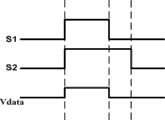
As shown in Figure 9, during pixel unit drive circuit work described in this second embodiment, the sequential chart of the output signal Vdata of the first control signal S1, the second control signal S2 and described data line;
Figure 10 A is that pixel unit drive circuit described in this second embodiment is at the equivalent circuit diagram of very first time section;
Figure 10 B is pixel unit drive circuit described in this second embodiment equivalent circuit diagram in the second time period;
Figure 10 C is pixel unit drive circuit described in this second embodiment equivalent circuit diagram in the 3rd time period;
As shown in Figure 10 A, in very first time section, it is the incipient stage, T1, T2, T3 all closes, T4, T5, T6 is for opening, if this previous stage, driving tube DTFT was closed condition, G point (node being connected with the grid of DTFT) is in vacant state, and the unlatching of T5, will make unsettled G point current potential seriously drop-down, DTFT is opened, if DTFT opens this previous stage itself, can enter the duty in this stage, due to opening of T4, DTFT is in diode connection status, data line passes through OLED, DTFT and T4 charge to memory capacitance Cs, the current potential that G is ordered is raise gradually, until G point current potential Vg=Vdata-Vth_oled-|Vth|, DTFT closes, P point (node being connected with the second end of described memory capacitance) current potential Vp=VSS, the voltage difference at memory capacitance Cs two ends is Vc=Vg-Vp=Vdata-Vth_oled-|Vth|-VSS, wherein, Vth_oled is the luminous critical cross-pressure of OLED, Vth is the threshold voltage of DTFT,
As shown in Figure 10 B, in the second time period, be buffer stage, T1 opens, and T2, T3, T4, T5, T6 close, DTFT also closes, in work halted state, to avoid, because the switching of switch produces unnecessary noise, P point and G point are in vacant state, the voltage Vc at memory capacitance Cs two ends is still constant, Vc=Vg-Vp=Vdata-Vth_oled-|Vth|-VSS;
As shown in Figure 10 C, in the 3rd time period, T4, T5, T6 closes, T1, T2, T3 opens, due to P point current potential, by VSS saltus step, to VDD-Voled, (Voled is the operating voltage of OLED under GTG for this reason, with Vth_oled inconsistent), and the grid of DTFT is in vacant state, therefore the voltage jump of Vg is Vdata-Vth_oled-|Vth|-VSS+VDD-Voled, the now source electrode of DTFT and voltage difference Vsg=VDD-Voled-Vg=VDD-Voled-(the Vdata-Vth_oled-|Vth|-VSS+VDD-Voled)=VSS+Vth_oled+|Vth|-Vdata between grid, DTFT works, and flows through electric current I=K (Vsg-|Vth|) of DTFT
2=K (VSS+Vth_oled+|Vth|-Vdata-|Vth|)
2=K (VSS+Vth_oled-Vdata)
2, OLED starts luminous, until next frame, wherein, the current coefficient that K is DTFT,
μ, C
oX, W, L be respectively the field-effect mobility of DTFT, gate insulation layer unit-area capacitance, channel width, length;
It doesn't matter can to find to flow through the electric current I of DTFT and the threshold voltage vt h of DTFT, so can improve the homogeneity of electric current, reaches the even of brightness; And flow through in the computing formula of electric current I of DTFT simultaneously, comprised Vth_oled, prolongation along with service time, OLED material aging luminescence efficiency declines, Vth_oled can rise, and the rising of Vth_oled makes the corresponding increase of working current, so improved the panel luminance reduction that material aging causes.
Figure 11 A is that pixel unit drive circuit described in the 3rd embodiment is at the equivalent circuit diagram of very first time section;
Figure 11 B is pixel unit drive circuit described in the 3rd embodiment equivalent circuit diagram in the second time period;
Figure 11 C is pixel unit drive circuit described in the 3rd embodiment equivalent circuit diagram in the 3rd time period.
In the pixel unit drive circuit described in second embodiment of the invention, Vdata must be that the negative voltage that absolute value is larger just can make whole circuit luminous, otherwise DTFT cannot open, not this restriction in the pixel unit drive circuit described in third embodiment of the invention, Vdata only needs less positive voltage just can make DTFT open and work.The time sequential routine of the pixel unit drive circuit described in second embodiment of the invention stands good in the pixel unit drive circuit described in third embodiment of the invention, the operation of circuit is also just the same, just the pixel unit drive circuit described in third embodiment of the invention is when the 3rd time period, P point current potential is that (Voled is the operating voltage of OLED under GTG for this reason for VDD-Voled by VDD saltus step, with Vth_oled inconsistent), and the grid of DTFT is in vacant state), therefore G point current potential Vg saltus step is Vdata-Vth_oled-|Vth|-Voled, thereby voltage difference Vsg=Vs-Vg=VDD-Voled-(the Vdata-Vth_oled-|Vth|-Voled)=VDD-Vdata+Vth_oled+|Vth| between the source electrode of DTFT and grid, flow through electric current I=K (Vsg-|Vth|) of DTFT
2=I=K (VDD-Vdata+Vth_oled)
2, K is the current coefficient of DTFT,
μ, C
oX, W, L be respectively the field-effect mobility of DTFT, gate insulation layer unit-area capacitance, channel width, length.
As shown in figure 12, pixel unit drive circuit described in fifth embodiment of the invention and the pixel unit drive circuit described in sixth embodiment of the invention be in when work, the sequential chart of the output signal Vdata of the first control signal S1, the second control signal S2 and described data line.
Pixel unit drive circuit described in fifth embodiment of the invention is compared with the pixel unit drive circuit described in second embodiment of the invention, just DTFT is become to N-shaped thin film transistor (TFT), and the anode of OLED is moved to negative electrode, the course of work of circuit is also just the same, but the luminous problem that has aperture opening ratio in the end.
In the pixel unit drive circuit described in fifth embodiment of the invention, Vdata also must could open DTFT for larger positive voltage, pixel unit drive circuit described in sixth embodiment of the invention has overcome this problem, in the pixel unit drive circuit described in sixth embodiment of the invention, Vdata only needs less positive voltage just DTFT can be opened, and makes circuit normal operation.
The operating process of the pixel unit drive circuit described in circuit of the present invention the 5th embodiment is as follows:
In very first time section, T2, T3, T4 open, and T1, T5, T6 close, Vg=Vdata+Vth_oled+Vth;
In the second time period, T2, T3, T4, T5, T6 close, and T1 opens, circuit buffering;
In the 3rd time period, T1, T5, T6 open, T2, T3, T4 close, Vp is VSS+Voled by VDD saltus step, Vg saltus step is Vdata+Vth_oled+Vth+VSS+Voled-VDD, the source potential Vs=VSS+Voled of DTFT, thereby the voltage difference Vsg=Vdata+Vth_oled+Vth-VDD between the source electrode of DTFT and the grid of DTFT, flow through the electric current I=K (Vsg-|Vth|) that drives thin film transistor (TFT) DTFT
2=K (Vdata+Vth_oled-VDD)
2; Wherein, the current coefficient that K is DTFT;
μ, C
oX, W, L be respectively the field-effect mobility of DTFT, gate insulation layer unit-area capacitance, channel width, length.
The operating process of the pixel unit drive circuit described in circuit of the present invention the 6th embodiment is as follows:
In very first time section, T2, T3, T4 open, and T1, T5, T6 close, Vg=Vdata+Vth_oled+Vth;
In the second time period, T2, T3, T4, T5, T6 close, and T1 opens, circuit buffering;
In the 3rd time period, T1, T5, T6 open, and T2, T3, T4 close, Vp is VSS+Voled by VSS saltus step, and Vg saltus step is Vdata+Vth_oled+Vth+Voled, Vs=VSS+Voled, Vgs=Vdata+Vth_oled+Vth-VSS, flows through electric current I=K (Vgs-|Vth|) of DTFT
2=K (Vdata+Vth_oled-VSS)
2; Wherein, the current coefficient that K is DTFT;
μ, C
oX, W, L be respectively the field-effect mobility of DTFT, gate insulation layer unit-area capacitance, channel width, length.
Than the pixel unit drive circuit described in second embodiment of the invention, the pixel unit drive circuit described in fifth embodiment of the invention, pixel unit drive circuit described in third embodiment of the invention, the pixel unit drive circuit described in sixth embodiment of the invention have reduced the magnitude of voltage of data voltage Vdata, when having reduced pixel unit drive circuit power consumption, also reduced the complexity of pixel unit drive circuit.
The maximum feature of pixel unit drive circuit of the present invention is that data voltage Vdata is from the source electrode input of DTFT, utilize the diode of DTFT to connect self discharge by Vth (threshold voltage of DTFT), Vdata (data voltage), Vth_oled (the luminescence threshold voltage of OLED) deposits in memory capacitance Cs, the critical voltage of the driving thin film transistor (TFT) of compensation OLED, the drive current that simultaneously utilizes the rising of voltage back coupling mechanism compensation OLED material aging critical voltage to cause declines.
The present invention also provides a kind of pixel cell driving method, and it is applied to above-mentioned pixel unit drive circuit, and described pixel cell driving method comprises the following steps:
Pixel charge step: first charging control unit is controlled and driven thin film transistor (TFT) to open, and controls memory capacitance is charged, until drive the grid potential of thin film transistor (TFT) to be increased to, described driving thin film transistor (TFT) cuts out;
Driving OLED luminescence display step: driving control unit is controlled the conducting of described driving thin film transistor (TFT) and its grid in vacant state, with driving OLED luminescence display and make the gate source voltage of described driving thin film transistor (TFT) compensate the threshold voltage of described driving thin film transistor (TFT).
The present invention also provides a kind of pixel cell, comprises the pixel unit drive circuit described in OLED and this first embodiment, this second embodiment and the 3rd embodiment;
The source electrode of driving thin film transistor (TFT) and the negative electrode of described OLED that described pixel unit drive circuit comprises are connected, the anode of described OLED is connected with the high level output end of driving power by described driving control unit, and the drain electrode of described driving thin film transistor (TFT) is connected with the low level output end of described driving power by described charging control unit.
The present invention also provides a kind of pixel cell, comprises the pixel unit drive circuit described in OLED and the 4th embodiment, the 5th embodiment and the 6th embodiment;
The source electrode of driving thin film transistor (TFT) that described pixel unit drive circuit comprises and the anodic bonding of described OLED, the negative electrode of described OLED is connected with the low level output end of driving power by described charging control unit, and the drain electrode of described driving thin film transistor (TFT) is connected with the high level output end of described driving power by described driving control unit.
More than explanation is just illustrative for the purpose of the present invention; and nonrestrictive, those of ordinary skills understand, in the situation that do not depart from the spirit and scope that claims limit; can make many modifications, variation or equivalence, but all will fall within the scope of protection of the present invention.
Claims (7)
1. a pixel unit drive circuit, for driving OLED, is characterized in that, comprise and drive thin film transistor (TFT), the first on-off element, memory capacitance, driving control unit and charging control unit, wherein,
The grid of described driving thin film transistor (TFT), is connected with the first end of described memory capacitance, also by described charging control unit, is connected with the drain electrode of described driving thin film transistor (TFT);
The source electrode of described driving thin film transistor (TFT), is connected with described OLED, and is connected with the second end of described memory capacitance by described driving control unit;
The drain electrode of described driving thin film transistor (TFT), is connected with driving power by described the first on-off element;
The second end of described memory capacitance Cs, is also connected with described driving power by described charging control unit;
Described driving control unit, is also connected with described OLED with described driving power respectively;
Described charging control unit, is also connected with described OLED with data line respectively;
Described driving thin film transistor (TFT) is p-type thin film transistor (TFT);
The source electrode of described driving thin film transistor (TFT) is connected with the negative electrode of described OLED;
The drain electrode of described driving thin film transistor (TFT) is connected with the low level output end of driving power by described the first on-off element;
The second end of described memory capacitance is connected with the low level output end of described driving power by described charging control unit;
Described the first on-off element is the first film transistor, and described driving control unit comprises the second thin film transistor (TFT) and the 3rd thin film transistor (TFT), and described charging control unit comprises the 4th thin film transistor (TFT), the 5th thin film transistor (TFT) and the 6th thin film transistor (TFT);
Described the first film transistor, grid is connected with the first control line, and drain electrode is connected with the low level output end of described driving power, and source electrode is connected with the drain electrode of described driving thin film transistor (TFT);
Described the second thin film transistor (TFT), grid is connected with the second control line, and source electrode is connected with the high level output end of described driving power, the anodic bonding of drain electrode and described OLED;
Described the 3rd thin film transistor (TFT), grid is connected with the second control line, and source electrode is connected with the source electrode of described driving thin film transistor (TFT), and drain electrode is connected with the second end of described memory capacitance;
Described the 4th thin film transistor (TFT), grid is connected with the first control line, and drain electrode is connected with the first end of described memory capacitance, and source electrode is connected with the drain electrode of described driving thin film transistor (TFT);
Described the 5th thin film transistor (TFT), grid is connected with the first control line, and source electrode is connected with the low level output end of described driving power, and drain electrode is connected with the second end of described memory capacitance;
Described the 6th thin film transistor (TFT), grid is connected with the first control line, the anodic bonding of source electrode and described OLED, drain electrode is connected with data line;
Described the first film transistor, described the second thin film transistor (TFT) and described the 3rd thin film transistor (TFT) are all p-type thin film transistor (TFT)s, and described the 4th on-off element, described the 5th thin film transistor (TFT) and described the 6th thin film transistor (TFT) are N-shaped thin film transistor (TFT)s.
2. a pixel unit drive circuit, for driving OLED, is characterized in that, comprise and drive thin film transistor (TFT), the first on-off element, memory capacitance, driving control unit and charging control unit, wherein,
The grid of described driving thin film transistor (TFT), is connected with the first end of described memory capacitance, also by described charging control unit, is connected with the drain electrode of described driving thin film transistor (TFT);
The source electrode of described driving thin film transistor (TFT), is connected with described OLED, and is connected with the second end of described memory capacitance by described driving control unit;
The drain electrode of described driving thin film transistor (TFT), is connected with driving power by described the first on-off element;
The second end of described memory capacitance Cs, is also connected with described driving power by described charging control unit;
Described driving control unit, is also connected with described OLED with described driving power respectively;
Described charging control unit, is also connected with described OLED with data line respectively;
Described driving thin film transistor (TFT) is p-type thin film transistor (TFT);
The source electrode of described driving thin film transistor (TFT) is connected with the negative electrode of described OLED;
The drain electrode of described driving thin film transistor (TFT) is connected with the low level output end of driving power by described the first on-off element;
The second end of described memory capacitance is connected with the low level output end of described driving power by described charging control unit;
Described the first on-off element is the first film transistor, and described driving control unit comprises the second thin film transistor (TFT) and the 3rd thin film transistor (TFT), and described charging control unit comprises the 4th thin film transistor (TFT), the 5th thin film transistor (TFT) and the 6th thin film transistor (TFT);
Described the first film transistor, grid is connected with the first control line, and drain electrode is connected with the low level output end of described driving power, and source electrode is connected with the drain electrode of described driving thin film transistor (TFT);
Described the second thin film transistor (TFT), grid is connected with the second control line, and source electrode is connected with the high level output end of described driving power, the anodic bonding of drain electrode and described OLED;
Described the 3rd thin film transistor (TFT), grid is connected with the second control line, and source electrode is connected with the source electrode of described driving thin film transistor (TFT), and drain electrode is connected with the second end of described memory capacitance;
Described the 4th thin film transistor (TFT), grid is connected with the first control line, and drain electrode is connected with the first end of described memory capacitance, and source electrode is connected with the drain electrode of described driving thin film transistor (TFT);
Described the 5th thin film transistor (TFT), grid is connected with the first control line, and source electrode is connected with the second end of described memory capacitance, and drain electrode is connected with the high level output end of driving power;
Described the 6th thin film transistor (TFT), grid is connected with the first control line, the anodic bonding of source electrode and described OLED, drain electrode is connected with data line;
Described the first film transistor, described the second thin film transistor (TFT) and described the 3rd thin film transistor (TFT) are all p-type thin film transistor (TFT)s, and described the 4th on-off element, described the 5th thin film transistor (TFT) and described the 6th thin film transistor (TFT) are N-shaped thin film transistor (TFT)s.
3. a pixel unit drive circuit, for driving OLED, is characterized in that, comprise and drive thin film transistor (TFT), the first on-off element, memory capacitance, driving control unit and charging control unit, wherein,
The grid of described driving thin film transistor (TFT), is connected with the first end of described memory capacitance, also by described charging control unit, is connected with the drain electrode of described driving thin film transistor (TFT);
The source electrode of described driving thin film transistor (TFT), is connected with described OLED, and is connected with the second end of described memory capacitance by described driving control unit;
The drain electrode of described driving thin film transistor (TFT), is connected with driving power by described the first on-off element;
The second end of described memory capacitance Cs, is also connected with described driving power by described charging control unit;
Described driving control unit, is also connected with described OLED with described driving power respectively;
Described charging control unit, is also connected with described OLED with data line respectively;
Described driving thin film transistor (TFT) is N-shaped thin film transistor (TFT);
The source electrode of described driving thin film transistor (TFT) and the anodic bonding of described OLED;
The drain electrode of described driving thin film transistor (TFT) is connected with the high level output end of driving power by described the first on-off element;
The second end of described memory capacitance is connected with the high level output end of described driving power by described charging control unit;
Described the first on-off element is the first film transistor, and described charging control unit comprises the second thin film transistor (TFT), the 3rd thin film transistor (TFT) and the 4th thin film transistor (TFT), and described driving control unit comprises the 5th thin film transistor (TFT) and the 6th thin film transistor (TFT);
Described the first film transistor, grid is connected with the first control line, and drain electrode is connected with the drain electrode of described driving thin film transistor (TFT), and source electrode is connected with the high level output end of driving power;
Described the second thin film transistor (TFT), grid is connected with the first control line, and source electrode is connected with the second end of described memory capacitance, and drain electrode is connected with the high level output end of described driving power;
Described the 3rd thin film transistor (TFT), grid is connected with the first control line, and drain electrode is connected with the drain electrode of described driving thin film transistor (TFT), and source electrode is connected with the grid of described driving thin film transistor (TFT);
Described the 4th thin film transistor (TFT), grid is connected with the first control line, and source electrode is connected with data line, and drain electrode is connected with the negative electrode of described OLED;
Described the 5th thin film transistor (TFT), grid is connected with the second control line, and source electrode is connected with the second end of described memory capacitance, and drain electrode is connected with the source electrode of described driving thin film transistor (TFT);
Described the 6th thin film transistor (TFT), grid is connected with the second control line, and source electrode is connected with the negative electrode of described OLED, and drain electrode is connected with the low level output end of described driving power;
Described the second thin film transistor (TFT), described the 3rd thin film transistor (TFT) and described the 4th thin film transistor (TFT) are N-shaped thin film transistor (TFT), and described the first film transistor, the 5th thin film transistor (TFT) and described the 6th thin film transistor (TFT) are p-type thin film transistor (TFT).
4. a pixel unit drive circuit, for driving OLED, is characterized in that, comprise and drive thin film transistor (TFT), the first on-off element, memory capacitance, driving control unit and charging control unit, wherein,
The grid of described driving thin film transistor (TFT), is connected with the first end of described memory capacitance, also by described charging control unit, is connected with the drain electrode of described driving thin film transistor (TFT);
The source electrode of described driving thin film transistor (TFT), is connected with described OLED, and is connected with the second end of described memory capacitance by described driving control unit;
The drain electrode of described driving thin film transistor (TFT), is connected with driving power by described the first on-off element;
The second end of described memory capacitance Cs, is also connected with described driving power by described charging control unit;
Described driving control unit, is also connected with described OLED with described driving power respectively;
Described charging control unit, is also connected with described OLED with data line respectively;
Described driving thin film transistor (TFT) is N-shaped thin film transistor (TFT);
The source electrode of described driving thin film transistor (TFT) and the anodic bonding of described OLED;
The drain electrode of described driving thin film transistor (TFT) is connected with the high level output end of driving power by described the first on-off element;
The second end of described memory capacitance is connected with the high level output end of described driving power by described charging control unit;
Described the first on-off element is the first film transistor, and described charging control unit comprises the second thin film transistor (TFT), the 3rd thin film transistor (TFT) and the 4th thin film transistor (TFT), and described driving control unit comprises the 5th thin film transistor (TFT) and the 6th thin film transistor (TFT);
Described the first film transistor, grid is connected with the first control line, and drain electrode is connected with the drain electrode of described driving thin film transistor (TFT), and source electrode is connected with the high level output end of driving power;
Described the second thin film transistor (TFT), grid is connected with the first control line, and source electrode is connected with the low level output end of described driving power, and drain electrode is connected with the second end of described memory capacitance;
Described the 3rd thin film transistor (TFT), grid is connected with the first control line, and drain electrode is connected with the drain electrode of described driving thin film transistor (TFT), and source electrode is connected with the grid of described driving thin film transistor (TFT);
Described the 4th thin film transistor (TFT), grid is connected with the first control line, and source electrode is connected with data line, and drain electrode is connected with the negative electrode of described OLED;
Described the 5th thin film transistor (TFT), grid is connected with the second control line, and source electrode is connected with the second end of described memory capacitance, and drain electrode is connected with the source electrode of described driving thin film transistor (TFT);
Described the 6th thin film transistor (TFT), grid is connected with the second control line, and source electrode is connected with the negative electrode of described OLED, and drain electrode is connected with the low level output end of described driving power;
Described the second thin film transistor (TFT), described the 3rd thin film transistor (TFT) and described the 4th thin film transistor (TFT) are N-shaped thin film transistor (TFT), and described the first film transistor, the 5th thin film transistor (TFT) and described the 6th thin film transistor (TFT) are p-type thin film transistor (TFT).
5. a pixel cell driving method, it is applied to pixel unit drive circuit as claimed in claim 1, it is characterized in that, and described pixel cell driving method comprises the following steps:
Pixel charge step: first charging control unit is controlled and driven thin film transistor (TFT) to open, and controls memory capacitance is charged, until drive the grid potential of thin film transistor (TFT) to be increased to, described driving thin film transistor (TFT) cuts out;
Driving OLED luminescence display step: driving control unit is controlled the conducting of described driving thin film transistor (TFT) and its grid in vacant state, with driving OLED luminescence display and make the gate source voltage of described driving thin film transistor (TFT) compensate the threshold voltage of described driving thin film transistor (TFT).
6. a pixel cell, is characterized in that, comprises OLED and pixel unit drive circuit as claimed in claim 1 or 2;
The source electrode of driving thin film transistor (TFT) and the negative electrode of described OLED that described pixel unit drive circuit comprises are connected, the anode of described OLED is connected with the high level output end of driving power by described driving control unit, and the drain electrode of described driving thin film transistor (TFT) is connected with the low level output end of described driving power by described charging control unit.
7. a pixel cell, is characterized in that, comprises OLED and the pixel unit drive circuit as described in claim 3 or 4;
The source electrode of driving thin film transistor (TFT) that described pixel unit drive circuit comprises and the anodic bonding of described OLED, the negative electrode of described OLED is connected with the low level output end of driving power by described charging control unit, and the drain electrode of described driving thin film transistor (TFT) is connected with the high level output end of described driving power by described driving control unit.
Priority Applications (2)
| Application Number | Priority Date | Filing Date | Title |
|---|---|---|---|
| CN201210047893.6A CN102708793B (en) | 2012-02-27 | 2012-02-27 | Pixel unit driving circuit and method as well as pixel unit |
| PCT/CN2012/084015 WO2013127189A1 (en) | 2012-02-27 | 2012-11-02 | Pixel unit driving circuit, pixel unit driving method and pixel unit |
Applications Claiming Priority (1)
| Application Number | Priority Date | Filing Date | Title |
|---|---|---|---|
| CN201210047893.6A CN102708793B (en) | 2012-02-27 | 2012-02-27 | Pixel unit driving circuit and method as well as pixel unit |
Publications (2)
| Publication Number | Publication Date |
|---|---|
| CN102708793A CN102708793A (en) | 2012-10-03 |
| CN102708793B true CN102708793B (en) | 2014-02-19 |
Family
ID=46901500
Family Applications (1)
| Application Number | Title | Priority Date | Filing Date |
|---|---|---|---|
| CN201210047893.6A Active CN102708793B (en) | 2012-02-27 | 2012-02-27 | Pixel unit driving circuit and method as well as pixel unit |
Country Status (2)
| Country | Link |
|---|---|
| CN (1) | CN102708793B (en) |
| WO (1) | WO2013127189A1 (en) |
Families Citing this family (12)
| Publication number | Priority date | Publication date | Assignee | Title |
|---|---|---|---|---|
| CN102708793B (en) * | 2012-02-27 | 2014-02-19 | 京东方科技集团股份有限公司 | Pixel unit driving circuit and method as well as pixel unit |
| CN103226931B (en) * | 2013-04-27 | 2015-09-09 | 京东方科技集团股份有限公司 | Image element circuit and organic light emitting display |
| WO2015083136A1 (en) * | 2013-12-05 | 2015-06-11 | Ignis Innovation Inc. | Charge-based compensation and parameter extraction in amoled displays |
| CN103700346B (en) * | 2013-12-27 | 2016-08-31 | 合肥京东方光电科技有限公司 | Pixel-driving circuit, array base palte, display device and image element driving method |
| US20160063921A1 (en) * | 2014-08-26 | 2016-03-03 | Apple Inc. | Organic Light-Emitting Diode Display With Reduced Capacitive Sensitivity |
| CN104575393B (en) * | 2015-02-03 | 2017-02-01 | 深圳市华星光电技术有限公司 | AMOLED (active matrix organic light emitting display) pixel driving circuit and pixel driving method |
| CN104715725A (en) * | 2015-04-03 | 2015-06-17 | 京东方科技集团股份有限公司 | Pixel circuit, display device and drive method of display device |
| CN106531083A (en) * | 2016-12-15 | 2017-03-22 | 上海天马有机发光显示技术有限公司 | Pixel circuit compensation method, OLED display panel and compensation method thereof |
| CN108446051B (en) * | 2018-03-16 | 2020-10-30 | 深圳市华星光电技术有限公司 | Array substrate and touch display device |
| CN113077761B (en) * | 2020-01-06 | 2022-12-09 | 京东方科技集团股份有限公司 | Pixel circuit, pixel driving method and display device |
| CN113450695A (en) * | 2020-05-07 | 2021-09-28 | 重庆康佳光电技术研究院有限公司 | MicroLED pixel circuit, time sequence control method and display |
| CN113516942B (en) * | 2020-05-14 | 2022-05-13 | 合肥联宝信息技术有限公司 | Display control method and driving circuit |
Family Cites Families (6)
| Publication number | Priority date | Publication date | Assignee | Title |
|---|---|---|---|---|
| KR101214205B1 (en) * | 2005-12-02 | 2012-12-21 | 재단법인서울대학교산학협력재단 | Display device and driving method thereof |
| KR100719662B1 (en) * | 2006-02-28 | 2007-05-17 | 삼성에스디아이 주식회사 | Pixel and organic light emitting display and driving method using the pixel |
| CN101192374B (en) * | 2006-11-27 | 2012-01-11 | 奇美电子股份有限公司 | Organic luminous display panel and its voltage drive organic light emitting pixel |
| JP6041455B2 (en) * | 2009-06-30 | 2016-12-07 | エルジー ディスプレイ カンパニー リミテッド | Image display device and driving method of image display device |
| KR101152466B1 (en) * | 2010-06-30 | 2012-06-01 | 삼성모바일디스플레이주식회사 | Pixel and Organic Light Emitting Display Device Using the Same |
| CN102708793B (en) * | 2012-02-27 | 2014-02-19 | 京东方科技集团股份有限公司 | Pixel unit driving circuit and method as well as pixel unit |
-
2012
- 2012-02-27 CN CN201210047893.6A patent/CN102708793B/en active Active
- 2012-11-02 WO PCT/CN2012/084015 patent/WO2013127189A1/en active Application Filing
Also Published As
| Publication number | Publication date |
|---|---|
| CN102708793A (en) | 2012-10-03 |
| WO2013127189A1 (en) | 2013-09-06 |
Similar Documents
| Publication | Publication Date | Title |
|---|---|---|
| CN102708793B (en) | Pixel unit driving circuit and method as well as pixel unit | |
| CN102708791B (en) | Pixel unit driving circuit and method, pixel unit and display device | |
| CN102708794B (en) | Pixel unit driving circuit and method as well as pixel unit | |
| CN103996379B (en) | The pixel-driving circuit of Organic Light Emitting Diode and image element driving method | |
| CN102708792B (en) | Pixel cell driving circuit, pixel cell driving method, pixel cell and display device | |
| CN103778889B (en) | Organic light emitting diode circuit and driving method thereof | |
| CN102651194B (en) | Voltage driving pixel circuit, driving method thereof and display panel | |
| CN103400548B (en) | Pixel-driving circuit and driving method, display device | |
| CN102708785B (en) | Pixel unit circuit, working method therefore and organic light emitting diode (OLED) display device | |
| CN103198793B (en) | Pixel circuit, drive method and display device thereof | |
| CN102411893B (en) | Pixel driving circuit | |
| CN102023667B (en) | Regulator and organic light emitting diode display using the same | |
| CN102789761B (en) | Pixel circuit, driving method thereof and organic light emitting display | |
| EP3208793A1 (en) | Pixel circuit and driving method therefor, and organic light-emitting display | |
| CN103714778B (en) | Image element circuit, the driving method of image element circuit and display device | |
| CN105427805A (en) | Pixel driving circuit and method, display panel, and display apparatus | |
| CN103077680A (en) | Organic light-emitting diode (OLE) pixel driving circuit | |
| CN103165080A (en) | Pixel circuit and driving method and display device thereof | |
| CN105679244A (en) | AMOLED pixel driving circuit and pixel driving circuit | |
| CN102708789A (en) | Pixel unit driving circuit and method, pixel unit and display device | |
| CN105070250A (en) | Pixel driving circuit and driving method thereof, and display device | |
| CN205282058U (en) | Pixel drive circuit, display panel and display device | |
| CN102708790A (en) | Pixel unit driving circuit and method, pixel unit and display device | |
| CN105405404A (en) | Pixel circuit, driving method thereof, OLED display panel and display device | |
| CN102881253A (en) | Pixel circuit and thin film transistor rear panel |
Legal Events
| Date | Code | Title | Description |
|---|---|---|---|
| C06 | Publication | ||
| PB01 | Publication | ||
| C10 | Entry into substantive examination | ||
| SE01 | Entry into force of request for substantive examination | ||
| C14 | Grant of patent or utility model | ||
| GR01 | Patent grant |