CN102403999A - Semiconductor device - Google Patents
Semiconductor device Download PDFInfo
- Publication number
- CN102403999A CN102403999A CN201110251361.XA CN201110251361A CN102403999A CN 102403999 A CN102403999 A CN 102403999A CN 201110251361 A CN201110251361 A CN 201110251361A CN 102403999 A CN102403999 A CN 102403999A
- Authority
- CN
- China
- Prior art keywords
- frequency
- signal
- phase
- clock
- circuit
- Prior art date
- Legal status (The legal status is an assumption and is not a legal conclusion. Google has not performed a legal analysis and makes no representation as to the accuracy of the status listed.)
- Pending
Links
- 239000004065 semiconductor Substances 0.000 title claims abstract description 39
- 238000011084 recovery Methods 0.000 claims abstract description 17
- 230000000630 rising effect Effects 0.000 claims description 53
- 230000001360 synchronised effect Effects 0.000 claims description 19
- 239000000919 ceramic Substances 0.000 claims description 6
- 230000006641 stabilisation Effects 0.000 claims description 5
- 238000011105 stabilization Methods 0.000 claims description 5
- 230000001934 delay Effects 0.000 claims 1
- 230000003111 delayed effect Effects 0.000 claims 1
- 230000010355 oscillation Effects 0.000 claims 1
- 230000005540 biological transmission Effects 0.000 abstract description 11
- 230000007423 decrease Effects 0.000 abstract description 8
- 238000010586 diagram Methods 0.000 description 15
- 238000000034 method Methods 0.000 description 13
- 238000004891 communication Methods 0.000 description 10
- 238000012546 transfer Methods 0.000 description 8
- 230000008569 process Effects 0.000 description 7
- 239000000284 extract Substances 0.000 description 6
- 239000010453 quartz Substances 0.000 description 6
- VYPSYNLAJGMNEJ-UHFFFAOYSA-N silicon dioxide Inorganic materials O=[Si]=O VYPSYNLAJGMNEJ-UHFFFAOYSA-N 0.000 description 6
- 238000005516 engineering process Methods 0.000 description 4
- 230000006872 improvement Effects 0.000 description 4
- 238000013459 approach Methods 0.000 description 3
- 238000001514 detection method Methods 0.000 description 3
- 230000010354 integration Effects 0.000 description 3
- 238000012545 processing Methods 0.000 description 3
- 238000005070 sampling Methods 0.000 description 3
- 238000004088 simulation Methods 0.000 description 3
- 239000000872 buffer Substances 0.000 description 2
- 238000006243 chemical reaction Methods 0.000 description 2
- 230000003750 conditioning effect Effects 0.000 description 2
- 238000012937 correction Methods 0.000 description 2
- 238000000605 extraction Methods 0.000 description 2
- 230000004048 modification Effects 0.000 description 2
- 238000012986 modification Methods 0.000 description 2
- 230000004044 response Effects 0.000 description 2
- 238000001228 spectrum Methods 0.000 description 2
- 241001125929 Trisopterus luscus Species 0.000 description 1
- 230000008901 benefit Effects 0.000 description 1
- 230000015572 biosynthetic process Effects 0.000 description 1
- 230000008859 change Effects 0.000 description 1
- 230000000052 comparative effect Effects 0.000 description 1
- 230000001186 cumulative effect Effects 0.000 description 1
- 230000003247 decreasing effect Effects 0.000 description 1
- 230000001915 proofreading effect Effects 0.000 description 1
- 230000005855 radiation Effects 0.000 description 1
- 230000009467 reduction Effects 0.000 description 1
- 238000010187 selection method Methods 0.000 description 1
Images


Classifications
-
- H—ELECTRICITY
- H03—ELECTRONIC CIRCUITRY
- H03L—AUTOMATIC CONTROL, STARTING, SYNCHRONISATION OR STABILISATION OF GENERATORS OF ELECTRONIC OSCILLATIONS OR PULSES
- H03L7/00—Automatic control of frequency or phase; Synchronisation
- H03L7/06—Automatic control of frequency or phase; Synchronisation using a reference signal applied to a frequency- or phase-locked loop
- H03L7/08—Details of the phase-locked loop
- H03L7/085—Details of the phase-locked loop concerning mainly the frequency- or phase-detection arrangement including the filtering or amplification of its output signal
- H03L7/089—Details of the phase-locked loop concerning mainly the frequency- or phase-detection arrangement including the filtering or amplification of its output signal the phase or frequency detector generating up-down pulses
Landscapes
- Stabilization Of Oscillater, Synchronisation, Frequency Synthesizers (AREA)
- Synchronisation In Digital Transmission Systems (AREA)
Abstract
The present invention provides a semiconductor device. The semiconductor device includes a clock-and-data recovery circuit including a phase tracking loop that generates a phase difference signal indicating a phase difference between a reception clock generated from a transmission clock and an input signal and makes the reception clock track the input signal, a frequency tracking loop that performs control to make a frequency of the reception clock track a frequency of the input signal, the clock-and-data recovery circuit being configured to extract a data signal and a synchronization clock from the input signal and to control a phase and a frequency of the reception clock, a frequency error adjuster that increases or decreases a value indicated by a frequency adjustment signal according to a frequency difference signal generated based on the phase difference signal, and an oscillator that increases or decreases a frequency of the transmission clock based on the frequency adjustment signal.
Description
Cross-reference to related applications
The application proposes based on the Japanese patent application No.2010-190686 that submitted on August 27th, 2010 and requires its priority, incorporates its full content into this paper by reference.
Technical field
The present invention relates to a kind of semiconductor device; Be specifically related to a kind of semiconductor device that comprises clock and data recovery circuit and oscillating circuit; The input signal that this clock and data recovery circuit provides from the outside extracts data, and this oscillating circuit produces the clock signal that offers the clock and data recovery circuit.
Background technology
In recent years, the communication speed between the semiconductor device is improved.For communication means, parallel data transfer approach and serial data transfer method have been adopted.But, think that in recent years serial data transfer method is superior to the parallel data transfer approach with regard to increasing data transfer rate.Therefore, serial data transfer method is applied even more extensively.
In serial data transfer method, through utilizing tranmitting data register to come modulated data signal and being transmitted as serial data.Subsequently, acceptor circuit extracts sampling clock and data-signal from serial data.The clock and data recovery circuit is used for the extraction of sampling clock and data-signal.
In addition, the generation high precision clock is very important as tranmitting data register in serial data transfer method.Usually, this high precision clock utilizes quartz resonator to produce.But quartz resonator is very expensive.Therefore, this just becomes one of high reason of system cost.Therefore, the open No.2007-135189 of Japanese Unexamined Patent Application discloses a kind of technology, and it utilizes the resonator lower than the precision of quartz resonator to produce the high accuracy tranmitting data register.In addition; Japanese national phase patent application No.2008-535387 that announced, the PCT international application discloses a kind of technology of control clock signal frequency; This clock signal results from receiver-side based on the information that obtains from the signal that received, though its purpose and do not lie in the generation tranmitting data register.Disclosed technology among the open No.2007-135189 of Japanese Unexamined Patent Application below is described.
At first, Fig. 7 illustrates the block diagram of disclosed communication system 100 among the open No.2007-135189 of Japanese Unexamined Patent Application.As shown in Figure 7, communication system 100 comprises device 101 and main frame 102.Device 101 comprises their transmission/receiving circuits separately with main frame 102.In Fig. 7, the transmission/receiving circuit of device 101 only is shown.Device 101 receives signal RX from main frame 102.And device 101 is sent to main frame 102 with signal TX.Main frame 102 produces reference clocks through utilizing the reference signal of being processed by quartz resonator etc. that source 120 takes place, and operates based on this reference clock.Simultaneously, device 101 produces reference clock through utilizing the reference signal of being processed by ceramic resonator that source 103 takes place, and operates based on this reference clock.
Notice that device 101 comprises sets up unit 111, frequency error detector 112, frequency generator 113 and serializer 114 synchronously.Set up unit 111 synchronously and receive the signal RX that receives by device 101, and from this signal RX, extract clock and data.Subsequently, the clock of setting up unit 111 output extractions synchronously is as receiving signal RS and exporting the data conduct of extracting and set up signal SCS synchronously.And setting up unit 111 synchronously is parallel signal based on clock with data transaction, and exports this parallel signal as receiving data DT.Frequency error detector 112 receives this reception signal RS, sets up signal SCS, reference clock Fref and transmission signal TS synchronously.Subsequently, frequency error detector 112 detects and receives signal RS and send the difference on the frequency between the signal TS, and output frequency conditioning signal FCS thus.Signal TS is sent in frequency generator 113 outputs, and the frequency of this transmission signal TS is confirmed based on frequency adjustment signal FCS and reference clock Fref.Serializer 114 receives and sends signal TS and transmission data DR and export signal TX.
Notice that the frequency of the high precision clock that produces in the frequency of the reception signal RS that from signal RX, extracts through device 101 and the main frame 102 is identical.In device 101, send signal TS and produce based on this reception signal RS.That is, through utilizing the resonator that has low precision in the device 101 can produce high precision clock.
Summary of the invention
The application inventor has been found that following problem.In device 101, the phase difference that receives between signal RS and the transmission signal TS calculates through simulation process.Therefore, the problem of the open No.2007-135189 existence of Japanese Unexamined Patent Application is that the frequency error detection of sending signal TS needs for a long time.For example, suppose that sending signal TS is 1.5GHz, so just need counting to receive the error that signal RS just can detect 333ppm at least for 3000 times.
As stated, in device 101, there is the problem that can not produce high accurate clock signal.And high accurate clock signal is absolutely necessary for high-speed serial communication.In addition, in order to improve the communication speed that communication speed surpasses current use, need to improve the frequency of clock signal, thereby further improve its precision.Therefore, the problems referred to above become more serious.
First aspect present invention is a kind of semiconductor device; It comprises: the clock and data recovery circuit; This clock and data recovery circuit comprises PTL phase tracking loop; It produces the phase signal of the leading or phase delay of phase place between indication synchronised clock and the input signal, and makes the Phase Tracking phase of input signals of synchronised clock, and this clock and data recovery circuit also comprises frequency tracking loop; It carries out control so that the frequency of the frequency-tracking input signal of synchronised clock, and this clock and data recovery circuit is constructed to extract data-signal and corresponding to the sampling clock of this data-signal from input signal; The frequency error adjuster, it increases based on the difference on the frequency signal or reduces by the indicated value of frequency adjustment signal, and this difference on the frequency signal produces based on the phase signal in the frequency tracking loop; And oscillator, it is based on the frequency that is improved or reduced tranmitting data register by the indicated value of frequency adjustment signal.
The semiconductor device of illustrative aspects according to the present invention, phase place and phase of input signals with synchronised clock in the clock and data recovery circuit compare, and control the frequency of tranmitting data register based on the phase place comparative result.As a result, the semiconductor device of illustrative aspects can be carried out the frequency correction of tranmitting data register in the very short time according to the present invention.
The semiconductor device of illustrative aspects according to the present invention, generation has high-frequency high accurate clock signal the clock signal that can produce from the resonator with low precision.
Description of drawings
Above-mentionedly become obviously from making the description of some embodiment with other aspects, advantage and characteristic below in conjunction with accompanying drawing, in the accompanying drawings:
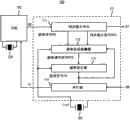
Fig. 1 is the block diagram of semiconductor device according to an embodiment of the invention;
Fig. 2 is the block diagram of the clock generating circuit of digital CDR, frequency error adjuster and synchronised clock according to an embodiment;
Fig. 3 is the block diagram according to the phase detectors of the semiconductor device of an embodiment;
Fig. 4 is according to the second integral device of the semiconductor device of an embodiment and the block diagram of mode generator;
Fig. 5 is the block diagram of the clock generating circuit of digital CDR, frequency error adjuster and synchronised clock according to another embodiment;
Fig. 6 is the block diagram of the clock generating circuit of digital CDR, frequency error adjuster and synchronised clock according to another embodiment; And
Fig. 7 is the block diagram of disclosed communication system among the open No.2007-135189 of Japanese Unexamined Patent Application.
Embodiment
First embodiment
Below with reference to the description of drawings embodiments of the invention.Fig. 1 illustrates the block diagram of semiconductor device 1 according to an embodiment of the invention.As shown in fig. 1, semiconductor device 1 comprises acceptor circuit 10, reference generator 11, PLL (phase-locked loop) circuit 12, clock and data recovery circuit (for example digital CDR) 13, frequency error adjuster 14, deserializer 15, serializer 16 and transmitter circuit 17.Semiconductor device 1 comprises transmission/receiving circuit and other treatment circuit (not shown).In the example depicted in fig. 1, acceptor circuit 10, digital CDR 13 and deserializer 15 constitute the circuit of receiver side, and the circuit of serializer 16 and transmitter circuit 17 formation transmitter sides.
In the present embodiment, digital CDR is as clock and data recovery circuit 13.Numeral CDR13 is made up of (a plurality of) logical circuit of handling binary message, and the digital signal of output indication information through using binary value is as the output signal.Numeral CDR 13 produces phase signal, and this phase signal indicates the receive clock RCLK that is produced by tranmitting data register CLK and the phase place between the input signal RD is leading or phase delay.And; Numeral CDR 13 comprises PTL phase tracking loop; It carries out control so that the phase place of the Phase Tracking input signal RD of receive clock RCLK, and digital CDR 13 also comprises frequency tracking loop, and it carries out control so that the frequency of the frequency-tracking input signal RD of receive clock RCLK.And digital CDR 13 extracts data-signal Sout and corresponding to the synchronised clock SCLK of this data-signal Sout from input signal RD, and phase place and the frequency of control receive clock RCLK.
Below with more detailed mode digital CDR 13, frequency error adjuster 14 and PLL circuit 12 in the parts of semiconductor device 1 are described particularly.Fig. 2 illustrates the block diagram of digital CDR 13, frequency error adjuster 14 and PLL circuit 12.
The phase difference that phase detectors 21 detect between receive clock RCLK and the input signal RD, and upgrade by the indicated polarity number of phase signal.In addition, phase detectors 21 are exported receive clock RCLK as synchronised clock SCLK, and from input signal RD, extract data-signal Sout.More particularly, the receive clock RCLK as synchronised clock SCLK is input to phase detectors 21.This receive clock RCLK comprises the first receive clock RCLK1 and the second receive clock RCLK3.Phase difference 180 degree of the phase place of the second receive clock RCLK3 and the first receive clock RCLK1.Phase detectors 21 output rising signals UP1 and dropping signal DOWN1 are as phase signal.When the phase delay of synchronised clock SCLK (the for example first receive clock RCLK1) during in the phase place of input signal RD, phase detectors 21 are changed to rising signals UP1 first logic level (for example high level) and dropping signal DOWN1 are changed to second logic level (for example low level).On the other hand, when the phase place of synchronised clock SCLK was ahead of the phase place of input signal RD, phase detectors 21 were changed to rising signals UP1 low level and dropping signal DOWN1 are changed to high level.
Fig. 3 illustrates the block diagram of phase detectors 21.As shown in Figure 3, phase detectors 21 only are made up of (a plurality of) logical circuit.Fig. 3 illustrates a kind of example of structure, wherein utilizes the two phase clock with 1.5GHz frequency to receive the data of 1.5Gbps.Phase detectors 21 comprise first trigger 41, second trigger 42, the 3rd trigger 43, latch 44, first XOR circuit (XOR) 45, second XOR circuit (XOR) 46, first data distributor (DEMUX circuit), 47, second data distributor (DEMUX circuit) 48, first or (OR) circuit 49, second or (OR) circuit 50, first inverter 51, second inverter 52, first and (AND) circuit 53 and second and (AND) circuit 54.
First XOR circuit (XOR) 45 receives the output q1 of first trigger 41 and the output q31 of latch 44.Second XOR circuit (XOR) 46 receives the output q11 of the 3rd trigger 43 and the output q31 of latch 44.First and second data distributors (DEMUX circuit) 47 and 48 receive respectively serial form, first and second XOR circuits (XOR) 45 and 46 output, and they are exported with parallel form.First or circuit 49 obtain first data distributor 47 output logic with.Second or circuit 50 obtain second data distributor 48 output logic with.The inverse value of the output of 51 outputs first of first inverter or circuit 49.The inverse value of the output of 52 outputs second of second inverter or circuit 50.First obtains first or the output of circuit 49 and second or the logical produc of the inverse value (it is exported through inverter 52) of the output of circuit 50 with circuit 53.Second obtains second or the output of circuit 50 and first or the logical produc of the inverse value of the output of circuit 49 with circuit 54.The output of first trigger 41 is also exported as data-signal Sout.In addition, receive clock RCLK1 also exports as synchronised clock SCLK.
Through above-mentioned structure, when the transmission timing of finding input signal RD was between the rising sequential of the rising edge of receive clock RCLK1 and receive clock RCLK3, phase detectors 21 were changed to high level with rising signals UP1, and dropping signal DOWN1 is changed to low level.On the other hand, when the transmission timing of finding input signal RD was between the rising sequential of the rising edge of receive clock RCLK3 and receive clock RCLK1, phase detectors 21 were changed to low level with rising signals UP1, and dropping signal DOWN1 is changed to high level.In addition, when each of data distributor had two and line output, the clock (not shown) that offers the circuit that is connected in phase detectors 21 following stages had the half the frequency of the frequency of the receive clock that offers phase detectors 21.
Next explanation is connected in the circuit of phase detectors 21 following stages.First integral device 22 increases or reduces first count value based on phase signal (for example rising signals UP1 and dropping signal DOWN1), and when first count value reaches predetermined value, exports rising signals UP2 or dropping signal DOWN2.That is, 22 pairs of first integral devices carry out integration by the indicated polarity number of phase signal.Notice that rising signals UP2 and dropping signal DOWN2 also can be called " first rising signals " and " first dropping signal " respectively.
Specifically, forward-backward counter is as first integral device 22.Capping count value and lower limit count value in this first integral device 22.In addition, when rising signals UP1 was high level, first integral device 22 increased by first count value according to clock.On the other hand, when decline signal DOWN1 was high level, first integral device 22 reduced by first count value according to clock.Subsequently, when first count value reached upper limit count value, first integral device 22 was changed to high level with rising signals UP2, and when first count value reached the lower limit count value, first integral device 22 was changed to high level with dropping signal DOWN2.
Second integral device 23 increases or reduces count value based on rising signals UP2 and dropping signal DOWN2, and the output count value is as difference on the frequency signal FP.More particularly, second integral device 23 is made up of forward-backward counter.When rising signals UP2 was in high level, second integral device 23 increased by second count value according to clock.On the other hand, when decline signal DOWN2 was in high level, second integral device 23 reduced by second count value according to clock.In addition, second integral device 23 outputs second count value is as difference on the frequency signal FP.Notice; Second integral device 23 according to present embodiment has following structure: second integral device 23 is through producing the intermediate frequency difference signal to rising signals UP2 and dropping signal DOWN2 integration, and increases or reduce second count value based on this intermediate frequency difference signal.
Fig. 4 illustrates the detailed diagram of second integral device 23 and mode generator 24.The details of second integral device 23 and mode generator 24 is described below with reference to Fig. 4.As shown in Figure 4, second integral device 23 comprises forward-backward counter 61 and forward-backward counter 62.In addition, mode generator 24 comprises counter 63 and decoder 64.
Capping count value and lower limit count value in forward-backward counter 61.In addition, when rising signals UP2 was in high level, forward-backward counter 61 increased integrated value according to clock.On the other hand, when decline signal DOWN2 was in high level, forward-backward counter 61 reduced integrated value according to clock.Subsequently, when integrated value reached upper limit count value, forward-backward counter 61 was changed to high level with rising signals UP2a, and when integrated value reached the lower limit count value, forward-backward counter 61 was changed to high level with dropping signal DOWN2a.
When forward-backward counter 62 had five counting width, the value of its output-31 to+31 was as second count value.This second count value is as difference on the frequency signal FP.When rising signals UP2a was in high level, forward-backward counter 62 increased by second count value according to clock.On the other hand, when decline signal DOWN2a was in high level, forward-backward counter 62 reduced by second count value according to clock.
Next, frequency error adjuster 14 below is described.As shown in Figure 2, frequency error adjuster 14 comprises adder 31, delay circuit 32 and multiplier 33.Adder 31 will by the indicated value of the output of delay circuit 32 with by the indicated value addition of difference on the frequency signal FP, and output end value.Delay circuit 31 keeps the output signal of adder 31, and the signal that after postponing clock of this signal, will keep outputs to adder 31.Multiplier 33 will be multiplied each other by indicated value of the output signal of adder 31 and the indicated value of gain signal that is provided by the outside, and regulate the relation between the frequency correction degree of output signal and tranmitting data register of adder 31 thus.The output signal of multiplier 33 is as frequency adjustment signal Fadj.That is, frequency error adjuster 14 is through increasing or reduce the indicated value by frequency adjustment signal Fadj from when beginning operation to carried out integration by the indicated value of difference on the frequency signal FP.
Next, the operation of the digital CDR 13 shown in the following key diagram 2, frequency error adjuster 14 and PLL circuit 12.In digital CDR 13, phase detectors 21 are made comparisons the phase place of input signal RD and the phase place of receive clock RCLK.Receive clock RCLK comprises a plurality of clock signals, and one of these a plurality of clock signals are as synchronised clock SCLK.Subsequently, phase detectors 21 output rising signals UP1 and dropping signal DOWN1, they indicate synchronised clock SCLK is delay or leading with respect to input signal RD.
22 couples of rising signals UP1 of first integral device and dropping signal DOWN1 ask average.Subsequently, first integral device 22 is based on asking average treatment output rising signals UP2 and dropping signal DOWN2.Rising signals UP2 and dropping signal DOWN2 are input to frequency mixer 25.Frequency mixer 25 is based on rising signals UP2 and dropping signal DOWN2 control rising signals UP4 and dropping signal DOWN4, and the phase place of proofreading and correct receive clock RCLK thus.By this way, digital CDR 13 excute phases control is so that the phase place of receive clock RCLK more approaches the phase place of input signal RD.
In addition, when the frequency of the frequency of input signal RD and receive clock RCLK not simultaneously, promptly when the frequency of the frequency of input signal RD and tranmitting data register CLK not simultaneously, digital CDR 13 compensates this difference on the frequency through utilizing difference on the frequency signal FP.
At first, when the frequency of input signal RD was lower than the frequency of receive clock RCLK, digital CDR 13 reduced the frequency of receive clock RCLK through the clock selection method of phase interpolator 26.In addition, frequency error adjuster 14 and PLL circuit 12 reduce the frequency of tranmitting data register CLK according to the difference on the frequency signal FP of digital CDR 13 outputs.
In the case, the phase place that phase detectors 21 detect receive clock RCLK is ahead of the phase place of input signal RD, and thus dropping signal DOWN1 is changed to high level.Subsequently, in response to dropping signal DOWN1 continuously, first integral device 22 is changed to high level with dropping signal DOWN2.Phase interpolator 26 postpones the phase place of receive clock RCLK based on this dropping signal DOWN2.But if although carrying out this phase control handles dropping signal DOWN1 and do not become low level, then dropping signal DOWN2 period of being in high level will become even be longer.As a result, the indicated value of difference on the frequency signal FP that is produced by second integral device 23 will reduce.
Along with becoming littler by the indicated value of difference on the frequency signal FP, mode generator 24 increases the cycle that dropping signal DOWN3 is changed to high level.On the other hand, along with becoming bigger by the indicated value of difference on the frequency signal FP, mode generator 24 increases the cycle that rising signals UP3 is changed to high level.That is, it is long more that dropping signal DOWN1 is changed to period of high level in phase detectors 21, and the period that then is changed to high level by the dropping signal DOWN3 of mode generator 24 outputs becomes long more.Subsequently, when decline signal DOWN2 and dropping signal DOWN3 became high level, frequency mixer 25 was changed to high level with dropping signal DOWN4.As a result, reduced the frequency of the receive clock RCLK that exports by phase interpolator 26 in fact.Subsequently; Along with the frequency of receive clock RCLK more near the frequency of (or become equal) input signal RD; Then becoming from high level period of the rising signals UP1 of phase detectors 21 output and dropping signal DOWN1 is equal to each other basically, makes the frequency stabilization of receive clock RCLK thus.
In addition, when difference on the frequency signal FP becomes more hour, the indicated value of frequency adjustment signal Fadj that is produced by frequency error adjuster 14 also becomes littler.As a result, PLL circuit 12 reduces the frequency dividing ratio of the frequency divider in the PLL circuit 12, reduces the frequency of tranmitting data register CLK thus.Along with the reduction of tranmitting data register CLK frequency, from also reducing through the frequency of inserting the receive clock RCLK that produces the signal that obtains in tranmitting data register CLK is carried out.
On the other hand, when the frequency of input signal RD was higher than the frequency of receive clock RCLK, phase detectors 21 detected the phase delay of receive clock RCLK in the phase place of input signal RD, and thus rising signals UP1 are changed to high level.Subsequently, in response to rising signals UP1 continuously, first integral device 22 is changed to high level with rising signals UP2.Phase interpolator 26 shifts to an earlier date the phase place of receive clock RCLK based on this rising signals UP2.But if although carrying out this phase control handles rising signals UP1 and do not become low level, then rising signals UP2 period of being in high level will become longer.As a result, the indicated value of difference on the frequency signal FP that is produced by second integral device 23 will increase.
Along with the value of difference on the frequency signal FP becomes bigger, mode generator 24 prolongs the period that rising signals UP3 is changed to high level.Subsequently, when rising signals UP2 and rising signals UP3 became high level, frequency mixer 25 was changed to high level with rising signals UP4.As a result, improved the frequency of the receive clock RCLK that exports by phase interpolator 26 in fact.Subsequently; Along with the frequency of receive clock RCLK more near the frequency of (or become equal) input signal RD; Then becoming from high level period of the rising signals UP1 of phase detectors 21 output and dropping signal DOWN1 is equal to each other basically, makes the frequency stabilization of receive clock RCLK thus.
In addition, when difference on the frequency signal FP became bigger, the indicated value of frequency adjustment signal Fadj that is produced by frequency error adjuster 14 also became bigger.As a result, PLL circuit 12 improves the frequency dividing ratio of the frequency divider in the PLL circuit 12, improves the frequency of tranmitting data register CLK thus.Along with the raising of tranmitting data register CLK frequency, from also improving through the frequency of inserting the receive clock RCLK that produces the signal that obtains in tranmitting data register CLK is carried out.
As stated, in semiconductor device 1, through in digital CDR 13, producing receive clock RCLK to inserting in the tranmitting data register CLK excute phase.Subsequently, digital CDR 13 produces difference on the frequency signal FP, is coming the difference on the frequency between reflected input signal RD and the tranmitting data register CLK from the phase difference between input signal RD and the receive clock RCLK on this difference on the frequency signal FP.Therefore, semiconductor device 1 can more early detect frequency departure, and improves the frequency-tracking ability of tranmitting data register CLK thus.
In correlation technique example shown in Figure 7, for example, under the situation of the input signal RD of 1.5GHz, need 3000 clock cycle (2nsec) detect the error of 333ppm.By contrast, in semiconductor device 1, suppose that the phase interpolation number of phase interpolator 26 is 64, then can in 47 clock cycle (3000 clock cycle 1/64th), detect the error of 333ppm.
In addition, in semiconductor device 1 according to this embodiment of the invention, the difference on the frequency signal FP that is produced by digital CDR13 produces in frequency loop, and this frequency loop is provided for the FREQUENCY CONTROL by the receive clock RCLK of digital CDR 13 execution at first.That is, in semiconductor device 1, need not to add any extra circuit with generation difference on the frequency signal FP, and thus the circuit area increase is minimized.
In addition; In semiconductor device 1 according to present embodiment; Even reference clock Fsrc is produced by the resonating device with low precision such as ceramic resonator, also can from reference clock Fsrc, produce high accuracy tranmitting data register CLK based on the input signal RD that has comprised high precision clock information.
In addition, in the semiconductor device 1 according to present embodiment, phase detectors 21 only are made up of (a plurality of) logical circuit.And phase detectors 21 detect the phase difference between input signal RD and the receive clock RCLK through digital processing.Notice, in having the clock and data recovery circuit of phase interpolator, utilize the Digital Signals phase interpolator usually.Therefore, when the phase difference between input signal RD and the receive clock RCLK detected through simulation process, the value that may need to detect converted digital value (analog-to-digital conversion process) into.This analog-to-digital conversion process usually and be not suitable for high speed processing.That is,, be difficult to control the frequency of tranmitting data register CLK based on high-frequency input signal RD through in the detection method of simulation process detected phase difference.The speed of serial data communication is just in cumulative year after year.Therefore, in this application, with high speed detection phase difference and very important to detected phase difference execution feedback processing.
Second embodiment
As another embodiment, the improvement example of digital CDR 13 is described.Fig. 5 illustrates the digital CDR 13a as the improvement example of digital CDR 13.Fig. 5 illustrates the block diagram corresponding to Fig. 2.As shown in Figure 5, digital CDR 13a comprises the first integral device 22a that substitutes first integral device 22.In this first integral device 22a, come capping count value and lower limit count value according to the maximum control signal.This maximum control signal is provided by other circuit (not shown).
The maximum control signal be used for when beginning operation upper limit count value and the absolute value of lower limit count value be set to smaller value.Subsequently, when the frequency stabilization of tranmitting data register CLK, the maximum control signal is used for upper limit count value and lower limit count value are set at following value, receives signal RXin when being in these values and shake is had the tolerance of increase.
The 3rd embodiment
As another embodiment, the improvement example of frequency error adjuster 14 is described.Fig. 6 illustrates the frequency error adjuster 14a as the improvement example of frequency error adjuster 14.Fig. 6 illustrates the block diagram corresponding to Fig. 2.As shown in Figure 6, frequency error adjuster 14a comprises frequency error adjuster 14 and holding circuit 34.That is, obtain frequency error adjuster 14a through holding circuit 34 being added to frequency error adjuster 14.
When the frequency stabilization of tranmitting data register CLK, the load signal that becomes enabled inputs to holding circuit 34 from other circuit (not shown).The value of holding circuit 34 holding frequency conditioning signal Fadj when load signal becomes enabled is as the frequency adjustment value.Subsequently, when starting, the delay circuit 32 that holding circuit 34 offers frequency error adjuster 14 with the frequency adjustment value that keeps is as the frequency adjustment initial value next time.In this way, frequency error adjuster 14a can just export the frequency adjustment signal Fadj that optimizes from the operation beginning, reduces the required time of tranmitting data register CLK convergence thus.
Though described the present invention, those skilled in the art will recognize that in the spirit of accompanying claims and scope and can come embodiment of the present invention, and the present invention be not limited to above-mentioned example with various modifications with regard to some embodiment.
And the scope of claim is not restricted to the described embodiments.Those skilled in the art can make up first to the 3rd embodiment as required.In addition, for example difference on the frequency signal FP indicates the amplitude of difference on the frequency and the value of polarity number simultaneously, maybe can be the value of only indicating polarity number.When difference on the frequency signal FP only indicates the polarity number of difference on the frequency, preferred use according to polarity number increase progressively (for example increasing progressively) with one or the adder of successively decrease (for example successively decreasing) with one as the adder 31 of frequency error adjuster 14.
And, notice that even possibly in the patent application process, carry out subsequent modification, but applicant's intention is to contain being equal to of all elements that require protection.
Claims (9)
1. semiconductor device comprises:
The clock and data recovery circuit; Comprise: PTL phase tracking loop; Said PTL phase tracking loop produces phase signal; Said phase signal is indicated from the receive clock of tranmitting data register generation and the phase place between the input signal is leading or phase delay, and makes the said phase of input signals of Phase Tracking of said receive clock; And frequency tracking loop; Said frequency tracking loop carries out control so that the frequency of the said input signal of frequency-tracking of said receive clock, and said clock and data recovery circuit is constructed to extract data-signal and corresponding to the synchronised clock of said data-signal and phase place and the frequency of controlling said receive clock from said input signal;
The frequency error adjuster, said frequency error adjuster increases according to the difference on the frequency signal that produces based on the said phase signal in the said frequency tracking loop or reduces by the indicated value of frequency adjustment signal; And
Oscillator, said oscillator is based on the frequency that is improved or reduced said tranmitting data register by the indicated value of said frequency adjustment signal.
2. semiconductor device according to claim 1, wherein said phase signal is indicated each of the leading and phase delay of phase place through one.
3. semiconductor device according to claim 1, wherein
Said clock and data recovery circuit comprises:
Phase detectors, said phase detectors detect the phase difference between said receive clock and the said input signal, and upgrade by the indicated polarity number of said phase signal;
The first integral device, said first integral device increases or reduces first count value based on said phase signal, and when said first count value reaches predetermined value, exports first rising signals and first dropping signal;
The second integral device, said second integral device increases or reduces second count value based on said first rising signals and said first dropping signal, and exports said second count value as said difference on the frequency signal;
Mode generator, said mode generator produces second rising signals and second dropping signal based on said difference on the frequency signal with predetermined space;
Frequency mixer, said frequency mixer produces phase place based on said first rising signals and said first dropping signal and said second rising signals and said second dropping signal and selects signal; And
Phase interpolator, said phase interpolator selects signal to select phase place through interior phase place of inserting said tranmitting data register according to said phase place, and output as a result clock as said synchronised clock,
Said PTL phase tracking loop comprises said phase detectors, said first integral device, said frequency mixer and said phase interpolator, and
Said frequency tracking loop comprises said phase detectors, said first integral device, said second integral device, said mode generator, said frequency mixer and said phase interpolator.
4. semiconductor device according to claim 3, wherein
Said first integral device is set to said predetermined value through the maximum control signal that the outside provides, and
Said maximum control signal is used for said predetermined value is set at: the value of said predetermined value before the frequency of said tranmitting data register satisfies predetermined stable case is less than the value after satisfying said stable case.
5. semiconductor device according to claim 1, wherein said frequency error adjuster comprises:
Adder, said adder will by the indicated value of said difference on the frequency signal with by the indicated value addition of the said frequency adjustment signal of previous time, and produce the said frequency adjustment signal of current time thus; And
Delay circuit, said delay circuit delays also offers said adder with delayed frequency adjustment signal from the said frequency adjustment signal of said adder output.
6. semiconductor device according to claim 5, wherein
Said frequency error adjuster comprises holding circuit, and said holding circuit is stored under the state of the frequency stabilization of said tranmitting data register by the indicated value of said frequency adjustment signal, and
Said delay circuit is exported the said value that is stored in the said holding circuit under initial condition.
7. semiconductor device according to claim 1 also comprises transmitter circuit, and said transmitter circuit sends data based on said tranmitting data register.
8. semiconductor device according to claim 1, wherein
Said oscillator comprises feedback loop, and said feedback loop produces said tranmitting data register and feeds back said tranmitting data register based on the frequency of reference clock, and
Said feedback loop comprises frequency divider, and said frequency adjustment signal is input to said frequency divider.
9. semiconductor device according to claim 8, wherein said reference clock is from ceramic resonator output or from controlling the variable oscillator output of its frequency of oscillation.
Applications Claiming Priority (2)
| Application Number | Priority Date | Filing Date | Title |
|---|---|---|---|
| JP2010190686A JP2012049863A (en) | 2010-08-27 | 2010-08-27 | Semiconductor device |
| JP2010-190686 | 2010-08-27 |
Publications (1)
| Publication Number | Publication Date |
|---|---|
| CN102403999A true CN102403999A (en) | 2012-04-04 |
Family
ID=45696327
Family Applications (1)
| Application Number | Title | Priority Date | Filing Date |
|---|---|---|---|
| CN201110251361.XA Pending CN102403999A (en) | 2010-08-27 | 2011-08-25 | Semiconductor device |
Country Status (3)
| Country | Link |
|---|---|
| US (1) | US8781054B2 (en) |
| JP (1) | JP2012049863A (en) |
| CN (1) | CN102403999A (en) |
Cited By (6)
| Publication number | Priority date | Publication date | Assignee | Title |
|---|---|---|---|---|
| CN102769455A (en) * | 2012-07-25 | 2012-11-07 | 苏州亮智科技有限公司 | High speed input/output interface and receiving circuit thereof |
| CN105786746A (en) * | 2015-01-12 | 2016-07-20 | 美国亚德诺半导体公司 | Apparatus And Methods For Clock And Data Recovery |
| CN106796563A (en) * | 2014-07-18 | 2017-05-31 | 高通股份有限公司 | For the system and method for chip to chip communication |
| CN107370720A (en) * | 2016-04-12 | 2017-11-21 | 基萨系统公司 | Multi-protocols and multiple data rates communication |
| CN107659392A (en) * | 2017-03-13 | 2018-02-02 | 广东高云半导体科技股份有限公司 | A kind of clock data recovery system |
| TWI815695B (en) * | 2021-11-23 | 2023-09-11 | 聯發科技股份有限公司 | Circuitry including clock and data recovery circuit |
Families Citing this family (8)
| Publication number | Priority date | Publication date | Assignee | Title |
|---|---|---|---|---|
| JP5792582B2 (en) | 2011-10-17 | 2015-10-14 | ルネサスエレクトロニクス株式会社 | Semiconductor device, receiver, transmitter, transceiver, and communication system |
| US9077349B2 (en) * | 2012-02-21 | 2015-07-07 | Qualcomm Incorporated | Automatic detection and compensation of frequency offset in point-to-point communication |
| KR102092253B1 (en) * | 2013-08-09 | 2020-03-24 | 에스케이하이닉스 주식회사 | Data recovery circuit and operating method thereof |
| JP6430738B2 (en) * | 2014-07-14 | 2018-11-28 | シナプティクス・ジャパン合同会社 | CDR circuit and semiconductor device |
| TWI555338B (en) * | 2014-11-14 | 2016-10-21 | 円星科技股份有限公司 | Phase detector and associated phase detecting method |
| US9490964B2 (en) | 2014-11-26 | 2016-11-08 | Qualcomm Incorporated | Symbol transition clocking clock and data recovery to suppress excess clock caused by symbol glitch during stable symbol period |
| US9401723B2 (en) * | 2014-12-12 | 2016-07-26 | Freescale Semiconductor, Inc. | XOR phase detector, phase-locked loop, and method of operating a PLL |
| US9979533B2 (en) * | 2016-09-02 | 2018-05-22 | Qualcomm Incorporated | Differentiating-integrating sampling data receiver |
Family Cites Families (8)
| Publication number | Priority date | Publication date | Assignee | Title |
|---|---|---|---|---|
| JPH084262B2 (en) * | 1986-03-31 | 1996-01-17 | 日本電気株式会社 | Bit synchronization circuit and method |
| KR100459879B1 (en) * | 1998-04-20 | 2005-01-15 | 삼성전자주식회사 | Nonlinear signal receiver, particularly with regards to stably recovering a sampling time in consideration of a nonlinear distortion of a reproduction signal when sampling the signal |
| US6794946B2 (en) * | 2000-05-22 | 2004-09-21 | Ramin Farjad-Rad | Frequency acquisition for data recovery loops |
| JP4657662B2 (en) * | 2004-09-10 | 2011-03-23 | ルネサスエレクトロニクス株式会社 | Clock and data recovery circuit |
| US7512203B2 (en) | 2005-03-30 | 2009-03-31 | Silicon Laboratories Inc. | Data cleaning with an asynchronous reference clock |
| JP4948077B2 (en) | 2005-10-14 | 2012-06-06 | ルネサスエレクトロニクス株式会社 | Transceiver and communication system using the same |
| JP2008263508A (en) * | 2007-04-13 | 2008-10-30 | Nec Electronics Corp | Clock and data recovery circuit |
| US8111800B2 (en) * | 2008-01-24 | 2012-02-07 | Applied Micro Circuits Corporation | Frequency ratio detection |
-
2010
- 2010-08-27 JP JP2010190686A patent/JP2012049863A/en active Pending
-
2011
- 2011-07-22 US US13/137,144 patent/US8781054B2/en active Active
- 2011-08-25 CN CN201110251361.XA patent/CN102403999A/en active Pending
Cited By (11)
| Publication number | Priority date | Publication date | Assignee | Title |
|---|---|---|---|---|
| CN102769455A (en) * | 2012-07-25 | 2012-11-07 | 苏州亮智科技有限公司 | High speed input/output interface and receiving circuit thereof |
| CN102769455B (en) * | 2012-07-25 | 2014-08-13 | 苏州亮智科技有限公司 | High speed input/output interface and receiving circuit thereof |
| CN106796563A (en) * | 2014-07-18 | 2017-05-31 | 高通股份有限公司 | For the system and method for chip to chip communication |
| CN106796563B (en) * | 2014-07-18 | 2020-01-14 | 高通股份有限公司 | System and method for chip-to-chip communication |
| CN105786746A (en) * | 2015-01-12 | 2016-07-20 | 美国亚德诺半导体公司 | Apparatus And Methods For Clock And Data Recovery |
| CN105786746B (en) * | 2015-01-12 | 2019-09-17 | 美国亚德诺半导体公司 | Device and method for clock and data recovery |
| CN107370720A (en) * | 2016-04-12 | 2017-11-21 | 基萨系统公司 | Multi-protocols and multiple data rates communication |
| CN107370720B (en) * | 2016-04-12 | 2020-10-09 | 基萨系统公司 | Multi-protocol and multi-data rate communications |
| CN107659392A (en) * | 2017-03-13 | 2018-02-02 | 广东高云半导体科技股份有限公司 | A kind of clock data recovery system |
| CN107659392B (en) * | 2017-03-13 | 2019-12-13 | 广东高云半导体科技股份有限公司 | clock data recovery system |
| TWI815695B (en) * | 2021-11-23 | 2023-09-11 | 聯發科技股份有限公司 | Circuitry including clock and data recovery circuit |
Also Published As
| Publication number | Publication date |
|---|---|
| US8781054B2 (en) | 2014-07-15 |
| US20120049910A1 (en) | 2012-03-01 |
| JP2012049863A (en) | 2012-03-08 |
Similar Documents
| Publication | Publication Date | Title |
|---|---|---|
| CN102403999A (en) | Semiconductor device | |
| US10630272B1 (en) | Measurement and correction of multiphase clock duty cycle and skew | |
| US6008680A (en) | Continuously adjustable delay-locked loop | |
| US4604582A (en) | Digital phase correlator | |
| US9496916B2 (en) | Semiconductor device, receiver, transmitter, transceiver and communication system | |
| US8803573B2 (en) | Serializer-deserializer clock and data recovery gain adjustment | |
| US9973196B2 (en) | Clock synchronizer | |
| EP3327461B1 (en) | Digital synthesizer, radar device and method therefor | |
| KR20040031389A (en) | Delay locked loop circuit for correcting duty cycle internally and duty cycle correction method thereof | |
| TWI417879B (en) | Delay locked loop circuit of semiconductor device | |
| US9832013B2 (en) | Phased clock error handling | |
| US6028462A (en) | Tunable delay for very high speed | |
| CN104242921A (en) | High-frequency delay-locked loop (DLL) and clock processing method thereof | |
| EP1913696B1 (en) | Delay-locked loop | |
| US10483989B2 (en) | Phase-locked loop, phase-locking method, and communication unit | |
| US6967536B2 (en) | Phase-locked loop circuit reducing steady state phase error | |
| US20110142119A1 (en) | Receiver circuit | |
| US8466911B2 (en) | Low voltage differential signal output stage | |
| US7573968B2 (en) | Data transmission circuit with serial interface and method for transmitting serial data | |
| JP5338631B2 (en) | Signal multiplexing circuit | |
| US7710818B2 (en) | Semiconductor memory device having low jitter source synchronous interface and clocking method thereof | |
| KR102342830B1 (en) | Multi-phase multiplying delaylocked loop based digital clock data recovery apparatus and method for recovery clock data | |
| US20240162906A1 (en) | Apparatus and method for optimum loop gain calibration for clock data recovery and phase locked loop | |
| JPH06311155A (en) | Clock signal extraction circuit |
Legal Events
| Date | Code | Title | Description |
|---|---|---|---|
| C06 | Publication | ||
| PB01 | Publication | ||
| C02 | Deemed withdrawal of patent application after publication (patent law 2001) | ||
| WD01 | Invention patent application deemed withdrawn after publication |
Application publication date: 20120404 |