CN102323700A - Reduce the system and method for the gamut in the display - Google Patents
Reduce the system and method for the gamut in the display Download PDFInfo
- Publication number
- CN102323700A CN102323700A CN2011103037555A CN201110303755A CN102323700A CN 102323700 A CN102323700 A CN 102323700A CN 2011103037555 A CN2011103037555 A CN 2011103037555A CN 201110303755 A CN201110303755 A CN 201110303755A CN 102323700 A CN102323700 A CN 102323700A
- Authority
- CN
- China
- Prior art keywords
- optical element
- display system
- light
- substrate
- display
- Prior art date
- Legal status (The legal status is an assumption and is not a legal conclusion. Google has not performed a legal analysis and makes no representation as to the accuracy of the status listed.)
- Pending
Links
Images


Classifications
-
- G—PHYSICS
- G02—OPTICS
- G02B—OPTICAL ELEMENTS, SYSTEMS OR APPARATUS
- G02B26/00—Optical devices or arrangements for the control of light using movable or deformable optical elements
- G02B26/08—Optical devices or arrangements for the control of light using movable or deformable optical elements for controlling the direction of light
-
- G—PHYSICS
- G02—OPTICS
- G02B—OPTICAL ELEMENTS, SYSTEMS OR APPARATUS
- G02B26/00—Optical devices or arrangements for the control of light using movable or deformable optical elements
- G02B26/001—Optical devices or arrangements for the control of light using movable or deformable optical elements based on interference in an adjustable optical cavity
-
- G—PHYSICS
- G02—OPTICS
- G02B—OPTICAL ELEMENTS, SYSTEMS OR APPARATUS
- G02B26/00—Optical devices or arrangements for the control of light using movable or deformable optical elements
Landscapes
- Physics & Mathematics (AREA)
- General Physics & Mathematics (AREA)
- Optics & Photonics (AREA)
- Spectroscopy & Molecular Physics (AREA)
- Mechanical Light Control Or Optical Switches (AREA)
- Micromachines (AREA)
Abstract
The present invention discloses a kind of system and method that reduces the gamut in the display; It comprises an interferometric modulator display, and said interferometric modulator display is configured to along one from least one light source and through said display and the observer's that arrives optical path passes at least for a moment optically focused from said light source and learns element reflects light.In one embodiment, said converging optical element comprises a diffraction optical element.
Description
The relevant information of dividing an application
This case is to divide an application.Female case of this division be that September 21, application number in 2005 are 200510103554.5 the applying date, denomination of invention is the application for a patent for invention case of " reducing the system and method for the gamut in the display ".
Technical field
Technical field of the present invention relates to MEMS (MEMS).
Background technology
MEMS (MEMS) comprises micromechanical component, driver and electronic component.Micromechanical component can adopt deposition, etching or other several portions that can etch away substrate and/or institute's deposited material layer maybe can add several layers and process with the micromachined technology that forms electricity and electromechanical assembly.One type MEMS device is called as interferometric modulator.Interferometric modulator can comprise the pair of conductive plate, one of them or the two all can be transparent whole or in part and/or be reflectivity, and can relative motion when applying a suitable electric signal.One of them plate can comprise the quiescent layer that is deposited on the substrate, and another plate can comprise the metal partion (metp) that separates through a clearance and this quiescent layer.Said apparatus is with a wide range of applications, and in this technology, utilizes and/or revises the characteristic of these types of devices so that its performance can be used for improving existing product and makes still undeveloped at present new product will be rather useful.
Summary of the invention
System of the present invention, method and device all have many aspects, and arbitrary single aspect all can not determine its desired characteristic separately.Now, its main characteristic is carried out brief description, this not delimit the scope of the invention.Checking this explanation, especially reading title for after the part of " embodiment ", how people provides the advantage that is superior to other display device if can understanding characteristic of the present invention.
One embodiment is a kind of display system that is used for display image.Said display system comprises a plurality of interference of light formula modulators that are incident on the surface thereof that are configured to modulate.Said display system further comprises a converging optical element, and its focal length that becomes to make said optical element with respect to a surface alignment of at least one interferometric modulator in a plurality of interferometric modulators is greater than the distance between said optical element and the said surface.
Another embodiment is a kind of method of manufacturing one display system.Said method is included in and forms a plurality of interferometric modulators on one first substrate.Said method further is included in and forms a converging optical element on one second substrate.The focal length that said optical element becomes to make said optical element with respect at least one surface alignment of at least one interferometric modulator in a plurality of interferometric modulators is greater than the distance between said optical element and said at least one surface.Another embodiment is a display system according to this method manufacturing.
Another embodiment is a kind of display system that is used for display image.Said display system comprises: be used for the member with interference mode modulation incident light on it; And being used for the member of converging light, this convergence member is through adjusting the gamut of at least a portion between different viewing location to limit said image.
Another embodiment is a kind of display system of making through the method that may further comprise the steps: on one first substrate, form a plurality of interferometric modulators; On one second substrate, form a convergence diffraction optical element, said optical element is positioned to be redirected at least one the lip-deep light that is incident at least one interferometric modulator in said a plurality of interferometric modulator.
Another embodiment is a kind of display system that is used for display image, and said display system comprises: be used for the member with interference mode modulation incident light on it; And be used for diffraction light and be incident in the said member that is used for the light on the member of interference mode light modulated to be redirected, the wherein said member that is used for diffraction light is configured to assemble said light.
Another embodiment is a kind of display system that is used to show an image, and said display system comprises: a plurality ofly be configured to modulate incident interference of light formula modulator on it; Reach one and be configured to be redirected the convergence diffraction optical element that is incident in the light at least one interferometric modulator in said a plurality of interferometric modulator.
Another embodiment is a kind of display system that is used for display image, and said display system comprises: be used for the member with interference mode modulation incident light on it; And be used for diffraction light and be incident in the said member that is used for the light on the member of interference mode light modulated to be redirected.
Description of drawings
Fig. 1 is an isometric drawing; It shows the part of an embodiment of an interferometric modulator display; Wherein one of one first interferometric modulator removable reflection horizon is in an off-position, and a removable reflection horizon of one second interferometric modulator is in an excited target position.
Fig. 2 is a system block diagram, and it shows that one comprises an embodiment of the electronic installation of one 3 * 3 interferometric modulator displays.
Fig. 3 is the removable mirror position of an exemplary embodiment of interferometric modulator shown in Figure 1 and the graph of a relation of the voltage that applies.
Fig. 4 is one group and can be used for driving the row of interferometric modulator display and the synoptic diagram of column voltage.
Fig. 5 A and Fig. 5 B show and can be used for writing the row of a frame of display data and an exemplary sequential chart of column signal to 3 * 3 interferometric modulator displays shown in Figure 2.
Fig. 6 A is the sectional view of a device shown in Figure 1.
Fig. 6 B is a sectional view of an alternate embodiment of an interferometric modulator.
Fig. 6 C is a sectional view of another alternate embodiment of an interferometric modulator.
Fig. 7 is the schematic side profile diagram of an embodiment of an interferometric modulator display, and it shows through an interferometric modulator element of the said display optical path from light source to an observer.
Fig. 8 is the schematic side profile diagram of another embodiment of interferometric modulator display; Similar with the interferometric modulator display shown in Fig. 7, said interferometric modulator display is comprising lens from light source in the optical path to the observer through interferometric modulator element.
Fig. 9 is the schematic side profile diagram of another embodiment of interferometric modulator display; Similar with the interferometric modulator display shown in Fig. 8, said interferometric modulator display is comprising a diffraction optical element from light source in the optical path to the observer through interferometric modulator element.
Figure 10 is the schematic side profile diagram of another embodiment of interferometric modulator display; Similar with the interferometric modulator display shown in Fig. 8, said interferometric modulator display is comprising a single-stage binary optical elements in the optical path to the observer from light source through interferometric modulator element.
Figure 11 A and 11B are system block diagrams, and it shows that one comprises an embodiment of the visual display unit of a plurality of interferometric modulators.
Embodiment
Below specify and relate to some embodiments of the invention.But, the present invention can implement through the different mode of many kinds.In this explanation, can be with reference to accompanying drawing, in the accompanying drawings, identical parts use identical number-mark from start to finish.
In preferred embodiment, the present invention includes the optical element that is positioned between interferometric display and the display observer, for example lens, Fresnel Lenses, diffraction optical element or binary optical elements.Said optical element is appreciable gamut when being configured to be reduced in viewing angle or angular variation.
Below specify and relate to some embodiments of the invention.But, the present invention can implement through the different mode of many kinds.In this explanation, can be with reference to accompanying drawing, in the accompanying drawings, identical parts use identical number-mark from start to finish.Find out easily that according to following explanation the present invention can be used for display image-no matter be dynamic image (for example video) or still image (for example rest image) in arbitrary configuration, no matter be character image or picture-device in implement.More specifically; The present invention can implement in inferior numerous kinds of electronic installations or is associated with these electronic installations for example (but being not limited to): mobile phone, wireless device, personal digital assistant (PDA), handheld computer or portable computer, gps receiver/omniselector, camera, MP3 player, video camera, game machine, wrist-watch, clock, counter, TV monitor, flat-panel monitor, computer monitor, automotive displays are (for example; Mileometer displays etc.), driving cabin control device and/or display, camera view display are (for example; The rear view camera display of vehicle), electronic photo, electronics billboard or label, projector, building structure, packing and aesthetic structures (for example, the image display of a jewelry).The MEMS device that has similar structures with MESE device described herein also can be used for non-demonstration application, for example is used for electronic switching device.
In Fig. 1, show a kind of interferometric modulator display embodiment that comprises an interfere type MEMS display element.In these devices, pixel is in bright state or dark state.Under bright (" opening (on) " or " opening (open) ") state, display element reflexes to the user with most of incident visible light.Be in dark (" closing (off) " or " closing (closed) ") state following time, display element reflects the incident visible light to the user hardly.Look various embodiment and decide, can put upside down the light reflectance properties that " on " reaches " off " state.The mainly reflection under selected color of the configurable one-tenth of MEMS pixel is also can realize colored the demonstration except that black and white.
Fig. 1 is an isometric drawing, and it shows two neighbors in a series of pixels of a visual displays, and wherein each pixel comprises a MEMS interferometric modulator.In certain embodiments, an interferometric modulator display comprises the row/column array that is made up of these interferometric modulators.Each interferometric modulator comprises a pair of reflection horizon, and this is positioned to each other to have a variable-sized optical resonance cavity at a distance of a variable and controlled distance at least to form one to the reflection horizon.In one embodiment, one of them reflection horizon can be moved between the two positions.Be called in this article on the primary importance of release conditions, the local reflex layer that the position of this displaceable layers distance one is fixed is far away relatively.On the second place, the position of this displaceable layers is more closely near this local reflex layer.Decide position according to removable reflection horizon, from the incident light of this two layers reflection can with mutually long or mutually the mode of disappearing interfere, thereby form the mass reflex or the non-reflective state of each pixel.
The pixel array portion that in Fig. 1, shows comprises two adjacent interferometric modulator 12a and 12b.In the interferometric modulator 12a in left side, demonstration one movably high reflection layer 14a is in an off-position, local reflex layer 16a one preset distance that this off-position distance one is fixed.In the interferometric modulator 12b on right side, demonstration one movably high reflection layer 14b is in an excited target position, and this excited target position is near fixing local reflex layer 16b.
Fixed bed 16a, 16b conduct electricity, the part is transparent and local is reflectivity, and can the layer of one or more respectively do for oneself chromium and tin indium oxides be processed through for example on a transparent substrates 20, depositing.Said each layer is patterned into parallel band, and can form the column electrode in the display device, as further specifying hereinafter.Displaceable layers 14a, 14b can form by one or more depositing metal layers that is deposited on pillar 18 tops (and column electrode 16a, 16b quadrature) and and be deposited on the series of parallel band that the middle expendable material between the pillar 18 constitutes.After expendable material was etched, these deformable metal levels separated with the air gap 19 of the metal level of fixing through a regulation.These deformable layer can use one to have high conductivity and reflexive material (for example aluminium), and those bands can form the row electrode in the display device.
When not applying voltage, cavity 19 remains between a layer 14a, the 16a, and deformable layer is in the mechanical relaxed state shown in pixel 12a among Fig. 1.Yet after a selected row and column applies potential difference (PD), the capacitor that forms at the respective pixel place of said row and column electrode intersection is recharged, and electrostatic force pulls to these electrodes together.If voltage is enough high, then displaceable layers generation deformation, and be forced on the fixed bed (can on fixed bed, deposit a dielectric material (not shown in this Figure), preventing short circuit, and the control separation distance), shown in the pixel 12b on right side among Fig. 1.Regardless of the potential difference (PD) polarity that is applied, the behavior is all identical.This shows, may command reflection and row/row of non-reflective pixel state encourage with traditional LCD and other display techniques in used row/row encourage similar in many aspects.
Fig. 2 to Fig. 5 shows the example process and the system that in a demonstration is used, use an interferometric modulator array.Fig. 2 is a system block diagram, and this figure shows that one can embody an embodiment of the electronic installation of each side of the present invention.In this exemplary embodiment; Said electronic installation comprises a processor 21 1, and it can be any general purpose single-chip or multicore sheet microprocessor; For example ARM,
 Pentium
 Pentium
 Pentium
Pro, 8051,
Pentium
Pro, 8051,
 Power
Power
 or any special microprocessor, for example digital signal processor, microcontroller or programmable gate array.According to convention in the industry, can
 processor 21 be configured to carry out one or more software modules.Except that carrying out an operating system, also can this processor be configured to carry out one or more software applications, comprise web browser, telephony application, e-mail program or any other software application.
In one embodiment, processor 21 also is configured to communicate with an array controller 22.In one embodiment, this array control unit 22 comprises horizontal drive circuit 24 and the column drive circuit 26 that signal is provided to a pel array 30.The xsect of the array shown in Fig. 1 illustrates with line 1-1 in Fig. 2.For the MEMS interferometric modulator, OK/hysteresis property of row excitation protocol these devices shown in Figure 3 capable of using.It possibly need the potential difference (PD) of (for example) 10 volts to make displaceable layers be deformed into actuated state from release conditions.Yet, when said voltage when this value reduces, along with said voltage drop is back to below 10 volts, said its state of displaceable layers maintenance.In the exemplary embodiment of Fig. 3, before voltage drop was low to moderate below 2 volts, displaceable layers can not discharge fully.Therefore, in instance shown in Figure 3, exist one to be approximately the voltage range that 3-7 lies prostrate, in this voltage range, exist one to apply voltage window, said device is stabilized in and discharges or actuated state in this window.Be referred to as " lag windwo " or " stability window " in this article.For the array of display that has hysteresis characteristic shown in Figure 3; OK/the row excitation protocol can be designed to make and be expert at during the gating; Make gating the pixel that is energized suffered about 10 volts voltage difference in capable, and make d/d pixel is suffered the voltage difference near 0 volt.After gating, make pixel suffer about 5 volts steady state voltage poor, gating makes its residing state so that its maintenance is expert at.After writing, in this example, each pixel is all born one and is in the interior potential difference (PD) of 3-7 volt " stability window ".This characteristic makes pixel design shown in Figure 1 be stabilized in an existing actuated state or release conditions under the voltage conditions in identical applying.Because each pixel of interferometric modulator; No matter be in actuated state or release conditions; In fact all be one by fixing and move the capacitor that the reflection horizon is constituted, so this steady state (SS) can be able to keep under the voltage in the lag windwo and consumed power hardly.If the current potential that is applied is fixed, then there is not electric current to flow into pixel basically.
In typical application, can be through confirming that according to one group of desired actuated pixels in first row one group of row electrode forms a display frame.After this, horizontal pulse is put on the electrode of the 1st row, thereby encourage the pixel corresponding with determined alignment.After this, with determined one group of row electrode become with second row in desired one group of actuated pixels corresponding.After this, pulse is put on the electrode of the 2nd row, thereby encourage the suitable pixel in the 2nd row according to determined row electrode.The pixel of the 1st row does not receive the influence of the pulse of the 2nd row, and the state that keeps it to set at the impulse duration of the 1st row.The property mode is to this process of capable repetition of whole series, to form said frame in order.Usually, repeating this process continuously through the speed with a certain required frame number/second to refresh and/or upgrade these frames with new video data.Also have a variety of row and the row electrodes that are used for the driving pixels array to be known by people, and can use with the present invention with the agreement that forms display frame.
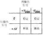
Fig. 4 and Fig. 5 show a kind of possible excitation protocol that is used on 3 * 3 arrays shown in Figure 2, forming a display frame.Fig. 4 shows one group of possible row and row voltage levvl of can be used for those pixels that show hysteresis curve shown in Figure 3.In the embodiment of Fig. 4, encourage a pixel to comprise suitable row are set to-V
Bias, and suitable row is set to+Δ V, it can correspond respectively to-5 volts and+5 volts.Discharging pixel then is through suitable row are set to+V
BiasAnd suitable row is set to identical+Δ V realizes so that form 0 volt potential difference (PD) at said pixel two ends.Wherein go voltages at those and remain in 0 volt the row, pixel is stable at its original residing state, and is in+V with these row
BiasStill-V
BiasIrrelevant.
Fig. 5 B is the sequential chart of a series of row of demonstration and column signal, and those signals put on 3 * 3 arrays shown in Figure 2, and it will form the demonstration shown in Fig. 5 A and arrange that wherein actuated pixels is non-reflectivity.Before writing the frame shown in Fig. 5 A, pixel can be in any state, and in this example, all row all are in 0 volt, and all row all be in+5 volts.Under these institute's voltages that apply, all pixels are stable at its existing actuated state or release conditions.
In the frame shown in Fig. 5 A, pixel (1,1), (1,2), (2,2), (3,2) and (3,3) are encouraged.For realizing this effect, during one " line time " of the 1st row, the 1st row and the 2nd row are set at-5 volts, the 3rd row are set at+5 volts.This can not change the state of any pixel, because all pixels all keep being in the stability window of 3-7 volt.After this, rise to 5 volts of pulses that are back to 0 volt that descend again then through one from 0 volt and come gating the 1st row.Actuate pixel (1,1) and (1,2) and discharge pixel (1,3) thus.Other pixels in the array are all unaffected.For the 2nd row is set at desired state, the 2nd row are set at-5 volts, the 1st row and the 3rd row are set to+5 volts.After this, apply identical strobe pulse with actuate pixel (2,2) and discharge pixel (2,1) and (2,3) to the 2nd row.Equally, other pixels in the array are all unaffected.Similarly, through the 2nd row and the 3rd row are set at-5 volts, and be listed as the 1st be set at+5 volts to the 3rd capable the setting.The strobe pulse of the 3rd row is set at the state shown in Fig. 5 A with the 3rd row pixel.After writing incoming frame, the row current potential is 0, and the row current potential can remain on+5 or-5 volts, and after this demonstration will be stable at the layout shown in Fig. 5 A.Should be appreciated that, can use identical programs the array that constitutes by tens of or hundreds of row and columns.The timing, order and the level that should also be clear that the voltage that is used to implement the row and column excitation can alter a great deal in above-described General Principle, and above-mentioned instance is merely exemplary, and any actuation voltage method all can be used with the present invention.
Detailed structure according to the interferometric modulator of above-mentioned principle operation can be ever-changing.For example, Fig. 6 A-6C shows three kinds of different embodiment of moving lens structure.Fig. 6 A is a sectional view embodiment illustrated in fig. 1, wherein deposition one strip of metal material 14 on the support member 18 that quadrature extends.In Fig. 6 B, movably reflecting material 14 only is on the tethers 32 at corner and is attached to support member.In Fig. 6 C, removable reflecting material 14 is suspended on the deformable layer 34.Because the structural design and the material therefor of reflecting material 14 can be optimized aspect optical property, and the structural design of deformable layer 34 and material therefor can be optimized aspect the desired mechanical property, so this embodiment has advantage.In many open files, comprise that for example No. 2004/0051929 U.S. discloses in the application case, the production of various dissimilar interference devices has been described.The technology that can use a variety of people to know is processed said structure, and this comprises a series of material depositions, patterning and etching step.
Fig. 7 is the schematic side profile diagram of an embodiment of an interferometric modulator display 100, and it shows through the optical path of display 100 from a light source 102 to one observers 130.Light source 102 shown in Fig. 7 is from a series of position emission light that comprise (for example) position 104 or 106.Interferometric modulator display 100 comprises the interferometric modulator array that is made up of 110a, 110b and 110c.Although in Fig. 7, shown an array that is made up of three photomodulators, the embodiment of display 100 can comprise thousands of or up to a million modulators.Among photomodulator 110a, 110b and the 110c each all comprises a pair of mirror 112 and 114. Mirror 112 and 114 is positioned to substantially parallel each other and interval one distance 116, to define an optical cavities betwixt.Color from the light that said optical cavities reflected depends on distance 116 at least in part.In an instance embodiment of the display 100 that is configured to produce a coloured image, the distance of selecting for each photomodulator 110a, 110b and 110c 116 makes each photomodulator 110a, 110b and 110c reflection be essentially the light of a particular color (for example red, blue or green).In other embodiments, the distance of all modulators 110 can be substantially the same in the display 100.
In one embodiment, display 100 produces a display image from multiple source along the light that a plurality of optical paths arrive display 100 through reflection.In an exemplary optical path, 120 arrive displays 100 along the path from the light of position 104.Interferometric modulator element 110a modulates this light, with will be along the path part of 120 light reflex to observer 130 along a path 122.120 incident light is with 122 reflected light defines an angle θ each other along the path along the path.Be transmitted to path (not shown) that observer 130 light propagated to be transmitted to the path that observer 130 light propagated by mirror 112 reflections by source 102 short by mirror 114 reflection and by source 102.Path length difference between this two paths has determined the peak wavelength of the light of the self-modulation device element 110a reflection that observer 130 feels together with other Several Factors.This path length difference roughly multiply by distance 116 with the cosine of angle θ/2 and is directly proportional.In θ=0 o'clock, cos θ/2=1, and path length difference is the twice of distance 116.Along with the increase of angle θ, cos θ/2 reduce, and are in fact become thus by the path distance (twices of distance 118) that these two mirrors 112 and 114 define for 120 and 122 the light along the path and to be shorter than the twice apart from 116.Be formed at the gamut of the optical path distances 118 of this shortening among the modulator element 110a corresponding to the light that reflects by modulator element 110a.When angle θ was enough big, observer 130 can feel this gamut in the color that display 120 is produced.
Fig. 8 is the schematic side profile diagram of another embodiment of interferometric modulator display 100, and interferometric modulator display 100 comprises the whole convergent lens 200 of watching the surface of a leap display 100.Lens 200 are positioned at apart from modulator 110 1 last less than the distance of the focal length of lens 200 along optical axis 201.In the embodiment that comprises lens 200 shown in Figure 8, an optical path comprises a route segment 202, and light 106 is transmitted to display 100 along route segment 202 from the position.In one embodiment, lens 200 have an optical aperture greater than total aperture of two or more interferometric modulators of display 100.In one embodiment, lens 200 have an optical aperture greater than total aperture of interferometric modulator array.Cross the surface reflection of lens 200 and the mirror through interferometric modulator 110a from least a portion transmission of the light of route segment 202.Reflected light transmission is once more crossed lens 200 arrival observers 130.In concept, lens 200 are selected to arrive observer 130 from the input transmittance ovennodulation device element 110a of a position 106 on the source 102.Therefore be chosen to the incident angle that incident angle (near 90 °) with the reflecting surface of modulator arrives observer's optical path in greater than the embodiment that is not having lens 200 through the optical path that lens 200 arrive observers' light.This transmittance to observer's 130 meetings are through changing the path length difference in the optical cavities so that institute's propagation distance more reduces the gamut of being felt near the distance that the light of propagating along optical axis 201 is followed.
In one embodiment, lens 200 be configured in fact through one comprise optical path section 202,220,222 and 122 optical path photoconduction is caused observer 130.The source of the light of 202 propagation is the position 106 on the source 102 along the path.Selected position 106 than the position 104 of sending the light of 120 propagation along the path more near the central axis of display system.In this embodiment of display 100, the reducing of light-source angle causes the angle of the light in the modulator element 110 littler in fact.Reflection paths section 222 defines one jiao of θ ' with incident path section 220.Lens 200 are chosen to make angle θ ' less than the angle θ that is defined by route segment 120 and 122 (corresponding to the light path in the display-middle existence that does not have the embodiment of lens-as shown in Figure 7).Diagonal angle θ ' the correspondence one that interferometric modulator element 110a place diminishes doubles distance 224 path length difference, and since θ ' less than θ, thereby path 224 will be longer than the path 118 among Fig. 7.Elongated path correspondingly reduces the gamut of being felt from axle light that is shown device 100 reflections.
In one embodiment; Display 100 is that a use has the direct-viewing type interferometric display that the light-struck light source 102 of broadband environment is watched; Wherein all basically points all receive similar irradiation in the observer field behind, so that not little with the equation of light from any other source position on average from the light of a source position.Therefore lens 200 are selected the light from such point in said: it is with respect to observer 130 diagonal angle selected angle when not having lens 200.
In one embodiment, convergent lens 200 is convex lens.The technology that technical field was known under the person of ordinary skill in the field can use draws shape and the material that is used for lens 200 are constructed with desired characteristic.Yet in many typical display application, for example in hand-held or other portable display apparatus, lens 200 are huge and heavy usually, and this is that people are undesirable.In addition, the structural support (not shown) that is used for lens 200 can increase the cost and the complexity of display 100, and can make thus lens 200 are integrated in such typical products and become unrealistic.
As a substitute of convergent lens 200, for example, for reducing this big volume, each embodiment can comprise any other converging optical element that is suitable for, and comprises Fresnel Lenses.Such as people hope, Fresnel Lenses is littler and light and handy than simple toroidal lens embodiment (lens 200 as shown in Figure 8).Yet for many portable use, or even the Fresnel Lenses that volume reduces is unrealisticly also still often big.Other embodiment of lens 200 can comprise the convergent lens or the optical element of any other known type of affiliated technical field.
To in photocontrol is used, using a kind of alternative of lens to be to use diffraction optical element, comprise holographic optical elements (HOE).At the conceptive diffraction optical element that can be considered progressively near an optical function (a for example Fresnel lens) is optical modulation element; It comprises in one embodiment and has used the photoetching technique patterning and be etched in the structure on the substrate; So that make optical diffraction with a definite in advance mode, for example make optical convergence or focusing.In one embodiment, said structure is of a size of several microns sizes, and this looks affected light wavelength is decided.Usually use a suitable computer program to calculate can to define one be used to carry out the DOE of a particular optical function (for example assemble lens function) the pattern and the shape of structure.The instance of this software comprises can be from being positioned at Pasadena; The Optical Resarch Associates of CA; The CODE V that Inc obtains, can be from being positioned at the Lambda Resarch Associates of Rochester NY; The OSLO that Inc obtains and can be from being positioned at Tucson, the ZEMAX that the Focus Software of AZ obtains.For example; More details about diffraction optical element; Comprise calculating, be found in " the diffraction optical element of being shown by Thomas J.Sulski, Alan D.Kathman, Dennis W.Prather: design, Computer-Assisted Design, Manufacture And Test (Diffractive Optics:Design, Fabrication &Test), Donald C.O ' Shea (Society of Photo-Optical Instrument Enginerring 2003) the lens arrangement that is suitable for.
One type DOE is binary optical elements (" BOE ").Binary optical elements is a kind of diffraction optical element that comprises a discrete number Difraction surface.The simplest form is to be made up of the single stage element with two Difraction surfaces (for example being formed by single lithography step).These two surfaces are introduced one and are 0 or are the differing of π in incident wavefront.One multistage binary element comprises that N level material-for example is through N lithography step formation.This N level can produce 2N phase level.
Fig. 9 is the schematic side profile diagram of an embodiment of interferometric modulator display 100, and interferometric modulator display 100 is comprising a diffraction optical element 302 through interferometric modulator element 110a in position 106 to observer 130 the optical path of light source 102.The embodiment of shown DOE 302 is the binary optical elements of a N=3.In other embodiments, N can be any numeral.In certain embodiments, N can be 1,2,3,4 or 5.In other embodiments, N can be within the scope of 1-10.
DOE 302 comprises one and assembles DOE.One assemble DOE be one be configured to carry out one assemble the optical function of lens DOE, even light is assembled towards the optical axis 201 of DOE 302.Should be appreciated that in each figure of Fig. 7-10 element that shown is neither draw in proportion, also have no intention the accurate illustration that is used to carry out the structure of the optical function of giving said element as any.Diffraction optical element (DOE) 302 comprises a large amount of small components 304 usually.Each element 304 comprises the lamination that is made up of single or a plurality of elements.Some this class component 304 can define a stepped shape.As stated, the size of element 304 and position typically use computing machine and calculate with the software that is suitable for.In one embodiment, said arrangements of elements is to define the pattern of one group of donut.In another embodiment, element 302 is grouped into the partial structurtes that can realize optical function described herein jointly.Element 304 photoetching techniques capable of using, use for example form with inferior suitable material: the photoresist of photoresist, sclerosis (for example in a baking oven, curing firmly), silica, quartz glass or plastics.In one embodiment, deposition and a series of elements 304 of etching with a specific thicknesses and refractive index materials layer with formation DOE 302.Therefore, the same with lens 200, DOE 302 selections come from the light of the position 106 of light source 102.At least a portion of this light is reflexed to observer 130 by interferometric modulator element 110a along route segment 122.
In one embodiment, DOE 302 is formed at one and is attached on the individual substrate of display 100.In one embodiment, said individual substrate comprises a film.Display 100 can comprise a diffuser (not shown), to be used for coming the reflected light of scattering by interferometric modulator element 110a reflection with lambert's pattern of a cardinal principle.In one embodiment, diffuser comprises DOE 302.In another embodiment, DOE 302 is formed on the same substrate with interferometric modulator 110a, 110b and the 110c of display 100.For example, interferometric modulator 110a, 110b and 110c can be formed on the glass substrate.In one embodiment, each interferometric modulator 110a, 110b and 110c are formed on one first side of said glass substrate, and DOE 302 is formed on the opposite side of said glass substrate.
In another embodiment, DOE 302 is formed on the same side with modulator 110.In such embodiment, element 304 is formed on the said substrate and by a complanation layer and covers.After this, on said complanation layer, form interferometric modulator 110a, 110b and 110c.In one embodiment, the refractive index of planarisation material is different with the refractive index of the material that is used to make diffraction element 304.The pattern of the diffraction element 304 in the DOE 302 is to calculate according to the two the refractive index of material that is used to form the material of diffraction element 304 and is used to form complanation layer.
In one embodiment, diffraction optical element 302 is formed by a binary optical elements simple, N=1.Figure 10 is the schematic side profile diagram of another embodiment of interferometric modulator display 100, and interferometric modulator display 100 is at an embodiment who in position 106 to observer 130 the optical path of light source 102, comprises the DOE 302 of N=1 through interferometric modulator element 110a.The embodiment of DOE 302 shown in Figure 10 utilizes one group of BOE structure 404 to form, and this group BOE structure 404 forms usually has roughly the same height or thickness each other.Although the exemplary DOE among Figure 10 302 is shown as the structure 404 that has between homogeneous phase, the also width of each structure 404 of scalable and optical function at interval to obtain to expect.In an illustrated embodiment, DOE 302 can be by single material layer through lithographic patterning and etching and form.The formation step of this embodiment of DOE 302 is less than the multistage binary optical elements 302 among Fig. 9.Can single-stage DOE 302 be placed on different positions and the different substrate, and to carry out complanation with preceding text to multistage DOE 302 described identical modes.
For example DOE 302 binary optical elements such as grade only define one with the approaching optical function of desired optical function.Generally speaking, the number of plies in the binary optical elements is many more, just can be more goodly near desired optical function.But, with the optical function of convergent lens 200 near having reduced the gamut that reflexes to observer 130 light from light source 102 and by interferometric modulator 110a at least in part.In certain embodiments, this part of gamut reduces the color accuracy that is enough to improve for the display of being felt for watching from the axle light source with from axle 100.
Any embodiment that is discussed with above combination DOE 302 is identical, can form the embodiment of DOE302 with display 100 relatively.For example, DOE 302 can be formed on the diffuser, one independently on the substrate or on the either side of the substrate of interferometric modulator 110a, 110b and 110c.
For bigger display, for example Diagonal Dimension is located at typical indoor viewing distance (for example several meters) greater than about 30 inches display, even if when being positioned at the center of display, the observer still can feel the angle gamut of a part of display.Should be appreciated that for example configurable one-tenth such as the embodiment of diffraction optical element 302 optical elements such as grade reduces this gamut of at least a portion of display.
The configurable one-tenth of the embodiment of diffraction optical element 302 is carried out other optical functions.For example, in certain embodiments maybe be in display be directed to a preferable viewing location scope with light.Therefore, in such embodiment, the also configurable one-tenth guiding of diffraction optical element 302 is from view direction or the control size of images of light to control visual field, restriction or expanded images of display 100.In one embodiment; Optical element comprises a biconvex lens assembly; This biconvex lens arrangement of components becomes through being directed to an angular range (for example, make from the light of display 100 horizontal axis around the display 100 distribute) visual field of (with respect to the observer) control display in the horizontal direction from the part of the light of display.In one embodiment, optical element makes angular range that light distributes along horizontal axis greater than the angular range that distributes along vertical axis.This can be increased in from axle viewing location place, the light quantity that for example the seat position range place around the display receives in a room.In one embodiment, diffraction optical element 302 further is configured to carry out the optical function of a biconvex lens.
In another embodiment, display 100 can comprise or be configured to use specific one or one group of light source with respect to the location aware of display 100.In this embodiment, diffraction optical element 302 is customized to according to the aperture of position, the quantity of illumination or light source and comes guide lights.In one embodiment, said light source comprises one or more light emitting diodes of arranging around the front of display 100 so that display is thrown light on.In this embodiment, DOE 302 is configured to change through (for example) and passes amount that DOE 302 is transmitted through the lip-deep light of display 100 and compensate said light source to the uneven irradiation of display or compensate the influence of other undesirable features of said light source.
Figure 11 A and 11B are the system block diagrams of an embodiment of demonstration one display device 2040.Display device 2040 for example can be cellular phone or mobile phone.Yet the same components of display device 2040 and the form of doing slightly to change thereof also can be used as the for example illustration of all kinds such as TV and portable electronic device display device.
The display 2030 of exemplary display device 2040 can be any in the numerous kinds of displays, comprises bi-stable display as herein described.In other embodiments; Display 2030 comprises flat-panel monitors such as plasma scope for example mentioned above, EL, OLED, STN LCD or TFT LCD or non-tablet display such as CRT or other tubular devices for example, and these displays are known by the person of ordinary skill in the field.Yet for ease of the explanation present embodiment, display 2030 comprises just like interferometric modulator display as herein described.
Figure 11 B schematically shows the assembly among the embodiment of exemplary display device 2040.Example illustrated property display device 2040 comprises a shell 2041, and can comprise that other are closed in assembly wherein at least in part.For example, in one embodiment, exemplary display device 2040 comprises a network interface 2027, and this network interface 2027 comprises that one is coupled to the antenna 2043 of a transceiver 2047.Transceiver 2047 is connected to processor 2021, and processor 2021 is connected to again regulates hardware 2052.Regulate hardware 2052 configurable paired signals and regulate (for example a signal being carried out filtering).Regulate hardware 2052 and be connected to a loudspeaker 2045 and a microphone 2046.Processor 2021 also is connected to an input media 2048 and a driving governor 2029.Driving governor 2029 is coupled to one frame buffer 2028 and is coupled to array driver 2022, and array driver 2022 is coupled to an array of display 2030 again.One power supply 2050 is all component power supply according to the designing requirement of particular exemplary display device 2040.
Network interface 2027 comprises antenna 2043 and transceiver 2047, so that exemplary display device 2040 can communicate through network and one or more device.In one embodiment, network interface 2027 also can have some processing capacity, to reduce the requirement to processor 2021.Antenna 2043 is any antennas that are used to launch and receive signal that the person of ordinary skill in the field knows.In one embodiment, this antenna is launched according to IEEE 802.11 standards (comprising IEEE 802.11 (a), (b), or (g)) and is received the RF signal.In another embodiment, this antenna is launched according to bluetooth (BLUETOOTH) standard and is received the RF signal.If be cellular phone, then this antenna is designed to receive CDMA, GSM, AMPS or other and is used for the convention signal that communicates at the mobile phone network.2047 pairs of signals that receive from antenna 2043 of transceiver carry out pre-service, so that it can be received and further handled by processor 2021.Transceiver 2047 is also handled the signal that self processor 2021 receives, so that they can be through antenna 2043 from exemplary display device 2040 emissions.
In an alternate embodiment, can replace transceiver 2047 by a receiver.In another alternate embodiment, can replace network interface 2027 by a figure image source, this figure image source can be stored or produce and send out the view data of delivering to processor 2021.For example, this figure image source can be the software module that hard disk drive or that digital video disk (DVD) or contains view data produces view data.
The overall operation of processor 2021 common control examples property display device 2040.Processor 2021 automatic network interfaces 2027 or a figure image source receive data (the for example view data of compression), and this data processing is become raw image data or is processed into a kind of form that is easy to be processed into raw image data.Then, the data after processor 2021 will be handled are sent to driving governor 2029 or are sent to frame buffer 2028 and store.Raw data typically refers to the information that can discern the picture characteristics of each position in the image.For example, said picture characteristics can comprise color, saturation degree and gray level.
In one embodiment, processor 2021 comprises a microcontroller, CPU or is used for the logical block of the operation of control examples property display device 2040.Adjusting hardware 2052 generally includes and is used for sending signals and being used for amplifier and the wave filter from microphone 2046 reception signals to loudspeaker 2045.Regulate hardware 2052 and can be the discrete component in the exemplary display device 2040, perhaps can incorporate in processor 2021 or other assemblies.
Driving governor 2029 direct self processors 2021 or receive the raw image data that produces by processor 2021 from frame buffer 2028, and suitably with said raw image data reformatting so that high-speed transfer to array driver 2022.Particularly, driving governor 2029 is reformated into one with raw image data and has the data stream of grating class form so that its have one be suitable for scanning array of display 2030 chronological order.Then, the information after driving governor 2029 will format is sent to array driver 2022.Although driving governor 2029 (for example lcd controller) is normally as an integrated circuit (IC) and being associated with system processor 2021 independently, yet these controllers also can make up by many kinds of modes.It can be used as hardware and is embedded in the processor 2021, is embedded in the processor 2021 or together fully-integrated with example, in hardware and array driver 2022 as software.
Usually; Array driver 2022 after driving governor 2029 receives format information and video data is reformated into one group of parallel waveform, the parallel waveform per second of this group many times is applied to from hundreds of of the x-y picture element matrix of display, thousands of lead-in wires sometimes.
In one embodiment, driving governor 2029, array driver 2022, and array of display 2030 be applicable to the display of arbitrary type as herein described.For example, in one embodiment, driving governor 2029 is a traditional display controller or bistable display controllers (a for example interferometric modulator controller).In another embodiment, array driver 2022 is a legacy drive or a bistable display driver (a for example interferometric modulator display).In one embodiment, a driving governor 2029 integrates with array driver 2022.This embodiment is very common in the integrated system of for example cellular phone, wrist-watch and other small-area display equal altitudes.In another embodiment, array of display 2030 is a typical array of display or a bistable array of display (for example one comprise an interferometric modulator array display).
In certain embodiments, as indicated above the staying of control programmability is stored in the driving governor, and this driving governor can be arranged on several positions of electronic display system.In some cases, the control programmability is stayed and is stored in the array driver 2022.The person of ordinary skill in the field will know, hardware that can any amount and/or component software and to implement above-mentioned optimization in the different configurations.
In view of the above, people will understand, embodiments of the invention through be an interferometric modulator display provide one can be reduced in the gamut that is manifested when viewing angle or ray angles change optical element overcome many problems of affiliated technical field.In addition, through using several additional lithography steps, promptly can this optical element be included in the display cost effective and efficient manner.
Although it is to show, explain and point out the novel feature that is applicable to various embodiment of the present invention that preceding text specify; Yet should be appreciated that; The person of ordinary skill in the field can make various omissions, substitute and change shown device or technology on form and details, and this does not deviate from spirit of the present invention.Should know,, thereby can embodiment of the present invention in the form of all characteristics as herein described and advantage be provided one because some characteristic can use with other characteristics or try out mutually independently.
Claims (72)
1. display system that is used to show an image, said display system comprises:
One reflection shows that it comprises a plurality of interferometric modulators, and said a plurality of interferometric modulators are through being configured to modulate the light that is incident on the surface thereof;
One converging optical element, its focal length that becomes to make said optical element with respect to a surface alignment of at least one interferometric modulator in said a plurality of interferometric modulators is greater than the distance between said optical element and the said surface;
Said optical element has a lens opening, and it is greater than both the total aperture in said a plurality of interferometric modulators;
Said optical element is configured to limit the gamut of at least a portion between different viewing location of said image; And
Wherein said gamut result from from said interferometric modulator that said image is associated in the light of at least some interferometric modulators in the reflection at said different viewing location place.
2. display system as claimed in claim 1, wherein said optical element comprise one have a convex surfaces lens.
3. display system as claimed in claim 1, wherein said optical element comprises a diffraction optical element.
4. display system as claimed in claim 1, wherein said optical element has an aperture, and it is greater than total aperture of said a plurality of interferometric modulators.
5. display system as claimed in claim 3, wherein said optical element comprise a binary optical elements.
6. display system as claimed in claim 3, wherein said optical element comprises a diffuser.
7. display system as claimed in claim 1, wherein said optical element comprises a biconvex lens.
8. display system as claimed in claim 3; Wherein said optical element is configured to make said modulated light to be different from along the distribution of one second axis of said display system along the distribution of a first axle of said display system; Wherein said first axle is a horizontal axis, and said second axis is a vertical axis.
9. display system as claimed in claim 3, it further comprises:
One light source, wherein said optical element are configured to compensate at least a optical property of said light source.
10. display system as claimed in claim 1, it further comprises:
One substrate, it supports said a plurality of interferometric modulator and supports said optical element.
11. display system as claimed in claim 10, wherein said substrate is between said optical element and said a plurality of modulator.
12. display system as claimed in claim 10, wherein said optical element is between said a plurality of interferometric modulators and said substrate.
13. display system as claimed in claim 10, wherein said a plurality of interferometric modulators are between said optical element and said substrate.
14. display system as claimed in claim 1, wherein said a plurality of interferometric modulators are configured to export colorama.
15. display system as claimed in claim 1, wherein said display system have one greater than 30 inches Diagonal Dimension.
16. a method of making a display system, said method comprises:
Form a reflection and show that it is included in a plurality of interferometric modulators on one first substrate; And
On one second substrate, form a converging optical element, the focal length that said optical element becomes to make said optical element with respect at least one surface alignment of at least one interferometric modulator in said a plurality of interferometric modulators is greater than the distance between said optical element and said at least one surface;
Said optical element has a lens opening, and it is greater than both the total aperture in said a plurality of interferometric modulators;
Said optical element is configured to limit the gamut of at least a portion between different viewing location of said image; And
Wherein said gamut result from from said interferometric modulator that said image is associated in the light of at least some interferometric modulators in the reflection at said different viewing location place.
17. method as claimed in claim 16 wherein forms said at least one optical element and is included in and deposits layer of material at least on the said substrate.
18. method as claimed in claim 17 wherein forms said at least one optical element and further comprises said at least one layer material patterning.
19. method as claimed in claim 16 wherein forms said at least one optical element and comprises formation one diffraction optical element.
20. method as claimed in claim 19 wherein forms said diffraction optical element and is included in binary optical elements of formation on the said substrate.
21. method as claimed in claim 19 wherein forms said diffraction optical element and comprises a patterns of materialization to form a plurality of diffractive optical elements.
22. method as claimed in claim 16, wherein said first substrate comprises said second substrate.
23. method as claimed in claim 16, wherein said optical element and said a plurality of modulator form and make said first substrate therebetween.
24. method as claimed in claim 16, wherein said optical element form between said a plurality of interferometric modulators and said first substrate.
25. method as claimed in claim 16, wherein said a plurality of interferometric modulators form between said optical element and said first substrate.
26. method as claimed in claim 16 wherein forms said optical element and comprises formation one biconvex lens.
27. method as claimed in claim 19 wherein forms said optical element and comprises and be configured to make said modulated light to be different from along the distribution of one second axis of said display system along the distribution of a first axle of said display system said optical element.
28. method as claimed in claim 19, it further comprises:
Arrange that a light source is to shine said optical element; And
Said optical element is configured to compensate at least a optical property of said light source.
29. method as claimed in claim 16, wherein said a plurality of interferometric modulators are configured to export colorama.
30. method as claimed in claim 16, wherein said display system have one greater than 30 inches Diagonal Dimension.
31. display system of making through the described method of arbitrary claim in the claim 16 to 30.
32. one kind make one be used to show the display system of an image method, said method comprises:
On one first substrate, form a plurality of interferometric modulators; And
On one second substrate, form a convergence diffraction optical element; Said optical element is positioned at least one the lip-deep light-redirecting that is incident at least one interferometric modulator in said a plurality of interferometric modulator, and wherein said optical element is configured to limit the gamut of at least a portion between different viewing location of said image.
33. method as claimed in claim 32 wherein forms said optical element and is included in and deposits layer of material at least on the said substrate.
34. method as claimed in claim 33 wherein forms said optical element and further comprises said at least one layer material patterning.
35. method as claimed in claim 32 wherein forms said optical element and is included in binary optical elements of formation on said second substrate.
36. method as claimed in claim 32 wherein forms said optical element and comprises a patterns of materialization to form a plurality of diffractive optical elements.
37. method as claimed in claim 32, wherein said first substrate comprises said second substrate.
38. method as claimed in claim 32, wherein said optical element and said a plurality of modulator form and make said first substrate therebetween.
39. method as claimed in claim 32, wherein said optical element form between said a plurality of interferometric modulators and said first substrate.
40. method as claimed in claim 32, wherein said a plurality of interferometric modulators form between said optical element and said first substrate.
41. method as claimed in claim 32 wherein forms said optical element and comprises formation one biconvex lens.
42. method as claimed in claim 32, wherein said optical element are configured to make said modulated light to be different from along the distribution of one second axis of said display system along the distribution of a first axle of said display system.
43. method as claimed in claim 42, wherein said first axle are a horizontal axis, and said second axis is a vertical axis.
44. method as claimed in claim 32, it further comprises:
Arrange that a light source is to shine said optical element; And
Further said optical element is configured to compensate at least a optical property of said light source.
45. display system of making through the described method of arbitrary claim in the claim 32 to 44.
46. a display system that is used to show an image, said display system comprises:
A plurality of interferometric modulators, it is configured to modulate incident light on it; And
One convergence diffraction optical element; It is configured to the light-redirecting at least one interferometric modulator that is incident in said a plurality of interferometric modulator, and wherein said optical element is configured to limit the gamut of at least a portion between different viewing location of said image.
47. display system as claimed in claim 46, wherein said optical element comprise a positive focal power optical element.
48. display system as claimed in claim 46, wherein said optical element comprise a binary optical elements.
49. display system as claimed in claim 46, wherein said optical element comprises a diffuser.
50. display system as claimed in claim 46, it further comprises:
One substrate, it supports said a plurality of interferometric modulator and supports said optical element.
51. display system as claimed in claim 50, wherein said substrate is between said optical element and said a plurality of modulator.
52. display system as claimed in claim 50, wherein said diffraction optical element is between said a plurality of interferometric modulators and said substrate.
53. display system as claimed in claim 50, wherein said a plurality of interferometric modulators are between said optical element and said substrate.
54. display system as claimed in claim 50, wherein said optical element are configured to make said modulated light to be different from along the distribution of one second axis of said display system along the distribution of a first axle of said display system.
55. display system as claimed in claim 54, wherein said first axle are a horizontal axis, and said second axis is a vertical axis.
56. display system as claimed in claim 46, it further comprises:
One light source, wherein said optical element are configured to compensate at least a optical property of said light source.
57. a display system that is used to show an image, said display system comprises:
Be used to reflect the member that shows an image, said member comprises: be used for the modulation member with interference mode modulation incident light on it; And
The member that is used for selective light; Said member with one than under the situation of selected member that need not said light more near the light around selecting perpendicular to the angle of said modulation member, to limit the gamut of at least a portion between different viewing location of said image through reflection.
58. display system as claimed in claim 57, wherein said reflection display member comprise that a reflection shows and said modulation member comprises one or more reflection interference type modulators.
59. display system as claimed in claim 57, it further comprises and is used to make said modulated light to be different from along the components distributed of one second axis of said display system along the distribution of a first axle of said display system.
60. display system as claimed in claim 57, the wherein said member that is used for selective light comprise a positive focal power optical element.
61. display system as claimed in claim 57, it further comprises the irradiation member, and the wherein said member that is used for selective light also comprises the member of the influence of at least a optical property that is used to compensate said irradiation member.
62. comprising, display system as claimed in claim 57, wherein said smooth selected member be used to make optical diffraction will be incident in the said member that is used for the light-redirecting on the member of interference mode light modulated.
63. display system as claimed in claim 62, wherein said modulation member comprises one or more interferometric modulators.
64. display system as claimed in claim 62, wherein said diffraction member comprises a diffraction optical element.
65. display system as claimed in claim 62, its further comprise be used to make said modulated light with a first axle components distributed along the different mode of one second axis of said display system along said display system.
66. display system as claimed in claim 62, it further comprises the member that is used to throw light on, and wherein said diffraction comprises and is used for the member that the influence at least a optical property of the said member that is used to throw light on compensates.
67. like the described display system of arbitrary claim in the claim 1,46 and 57, it further comprises:
One processor that communicates with said a plurality of interferometric modulator electricity, said processor is configured to image data processing; And
One memory storage that communicates with said processor electricity.
68. like the described display system of claim 67, it further comprises:
One drive circuit, it is configured to send at least one signal to said a plurality of interferometric modulators.
69. like the described display system of claim 68, it further comprises:
One controller, it is configured at least a portion of said view data is sent to said driving circuit.
70. like the described display system of claim 69, it further comprises:
One image source module, it is configured to send said view data to said processor.
71. like the described display system of claim 70, wherein said image source module comprise a receiver, transceiver, and transmitter at least one.
72. like the described display system of claim 67, it further comprises:
One input media, it is configured to receive the input data and said input data is sent to said processor.
Applications Claiming Priority (4)
| Application Number | Priority Date | Filing Date | Title |
|---|---|---|---|
| US61348204P | 2004-09-27 | 2004-09-27 | |
| US60/613,482 | 2004-09-27 | ||
| US11/041,020 | 2005-01-21 | ||
| US11/041,020 US7813026B2 (en) | 2004-09-27 | 2005-01-21 | System and method of reducing color shift in a display |
Related Parent Applications (1)
| Application Number | Title | Priority Date | Filing Date |
|---|---|---|---|
| CN 200510103554 Division CN1755432A (en) | 2004-09-27 | 2005-09-21 | System and method of reducing color shift in a display |
Publications (1)
| Publication Number | Publication Date |
|---|---|
| CN102323700A true CN102323700A (en) | 2012-01-18 |
Family
ID=35509317
Family Applications (1)
| Application Number | Title | Priority Date | Filing Date |
|---|---|---|---|
| CN2011103037555A Pending CN102323700A (en) | 2004-09-27 | 2005-09-21 | Reduce the system and method for the gamut in the display |
Country Status (12)
| Country | Link |
|---|---|
| US (3) | US7813026B2 (en) |
| EP (2) | EP2241923A1 (en) |
| JP (2) | JP5452833B2 (en) |
| KR (1) | KR101187215B1 (en) |
| CN (1) | CN102323700A (en) |
| AU (1) | AU2005203364A1 (en) |
| BR (1) | BRPI0503889A (en) |
| CA (1) | CA2514489A1 (en) |
| MX (1) | MXPA05010243A (en) |
| RU (1) | RU2005129954A (en) |
| SG (2) | SG121048A1 (en) |
| TW (1) | TWI438483B (en) |
Cited By (1)
| Publication number | Priority date | Publication date | Assignee | Title |
|---|---|---|---|---|
| CN114528880A (en) * | 2022-02-21 | 2022-05-24 | 北京理工大学 | Wavefront aberration measuring method based on computer generated hologram |
Families Citing this family (34)
| Publication number | Priority date | Publication date | Assignee | Title |
|---|---|---|---|---|
| US6674562B1 (en) | 1994-05-05 | 2004-01-06 | Iridigm Display Corporation | Interferometric modulation of radiation |
| US7907319B2 (en) * | 1995-11-06 | 2011-03-15 | Qualcomm Mems Technologies, Inc. | Method and device for modulating light with optical compensation |
| US8928967B2 (en) | 1998-04-08 | 2015-01-06 | Qualcomm Mems Technologies, Inc. | Method and device for modulating light |
| WO1999052006A2 (en) | 1998-04-08 | 1999-10-14 | Etalon, Inc. | Interferometric modulation of radiation |
| TWI289708B (en) | 2002-12-25 | 2007-11-11 | Qualcomm Mems Technologies Inc | Optical interference type color display |
| US7342705B2 (en) | 2004-02-03 | 2008-03-11 | Idc, Llc | Spatial light modulator with integrated optical compensation structure |
| US7710636B2 (en) * | 2004-09-27 | 2010-05-04 | Qualcomm Mems Technologies, Inc. | Systems and methods using interferometric optical modulators and diffusers |
| US7813026B2 (en) | 2004-09-27 | 2010-10-12 | Qualcomm Mems Technologies, Inc. | System and method of reducing color shift in a display |
| US7630123B2 (en) * | 2004-09-27 | 2009-12-08 | Qualcomm Mems Technologies, Inc. | Method and device for compensating for color shift as a function of angle of view |
| US8310441B2 (en) | 2004-09-27 | 2012-11-13 | Qualcomm Mems Technologies, Inc. | Method and system for writing data to MEMS display elements |
| US7508571B2 (en) | 2004-09-27 | 2009-03-24 | Idc, Llc | Optical films for controlling angular characteristics of displays |
| US7916980B2 (en) | 2006-01-13 | 2011-03-29 | Qualcomm Mems Technologies, Inc. | Interconnect structure for MEMS device |
| US7845841B2 (en) | 2006-08-28 | 2010-12-07 | Qualcomm Mems Technologies, Inc. | Angle sweeping holographic illuminator |
| WO2008045311A2 (en) | 2006-10-06 | 2008-04-17 | Qualcomm Mems Technologies, Inc. | Illumination device with built-in light coupler |
| EP1943551A2 (en) | 2006-10-06 | 2008-07-16 | Qualcomm Mems Technologies, Inc. | Light guide |
| JP2010510530A (en) | 2006-10-06 | 2010-04-02 | クォルコム・メムズ・テクノロジーズ・インコーポレーテッド | Optical loss structure integrated into lighting equipment |
| WO2008045463A2 (en) | 2006-10-10 | 2008-04-17 | Qualcomm Mems Technologies, Inc. | Display device with diffractive optics |
| US8111262B2 (en) * | 2007-05-18 | 2012-02-07 | Qualcomm Mems Technologies, Inc. | Interferometric modulator displays with reduced color sensitivity |
| KR101415566B1 (en) | 2007-10-29 | 2014-07-04 | 삼성디스플레이 주식회사 | Display device |
| US8068710B2 (en) * | 2007-12-07 | 2011-11-29 | Qualcomm Mems Technologies, Inc. | Decoupled holographic film and diffuser |
| WO2009102731A2 (en) * | 2008-02-12 | 2009-08-20 | Qualcomm Mems Technologies, Inc. | Devices and methods for enhancing brightness of displays using angle conversion layers |
| WO2009129264A1 (en) * | 2008-04-15 | 2009-10-22 | Qualcomm Mems Technologies, Inc. | Light with bi-directional propagation |
| US8736590B2 (en) | 2009-03-27 | 2014-05-27 | Qualcomm Mems Technologies, Inc. | Low voltage driver scheme for interferometric modulators |
| JP5285770B2 (en) * | 2009-05-29 | 2013-09-11 | シャープ株式会社 | Display device and driving method of display device |
| US8670171B2 (en) | 2010-10-18 | 2014-03-11 | Qualcomm Mems Technologies, Inc. | Display having an embedded microlens array |
| US8902484B2 (en) | 2010-12-15 | 2014-12-02 | Qualcomm Mems Technologies, Inc. | Holographic brightness enhancement film |
| US9164219B2 (en) | 2011-11-14 | 2015-10-20 | Nano-Optic Devices, Llc | Frontlight unit for reflective displays |
| US8596846B2 (en) | 2012-03-16 | 2013-12-03 | Nano-Optic Devices, Llc | Frontlight unit for enhancing illumination of a reflective display |
| US9325948B2 (en) | 2012-11-13 | 2016-04-26 | Qualcomm Mems Technologies, Inc. | Real-time compensation for blue shift of electromechanical systems display devices |
| US9477690B2 (en) * | 2013-02-04 | 2016-10-25 | Nokia Technologies Oy | Method and apparatus for measuring information associated with another device |
| CN104951136B (en) * | 2015-07-06 | 2018-01-19 | 京东方科技集团股份有限公司 | Touch base plate and preparation method thereof and display device |
| CN107688264A (en) * | 2016-08-05 | 2018-02-13 | 元太科技工业股份有限公司 | Electrophoretic display apparatus |
| CN106441574B (en) * | 2016-09-13 | 2018-01-02 | 成都宏志微纳光电技术有限公司 | A kind of miniature wide spectrum spectrometer |
| JP7040982B2 (en) | 2018-03-30 | 2022-03-23 | 株式会社エクセルシャノン | Joinery |
Citations (1)
| Publication number | Priority date | Publication date | Assignee | Title |
|---|---|---|---|---|
| US20020126364A1 (en) * | 1994-05-05 | 2002-09-12 | Iridigm Display Corporation, A Delaware Corporation | Interferometric modulation of radiation |
Family Cites Families (690)
| Publication number | Priority date | Publication date | Assignee | Title |
|---|---|---|---|---|
| US450171A (en) * | 1891-04-14 | Wire gate | ||
| US560441A (en) * | 1896-05-19 | Hale to charles g | ||
| US2534846A (en) | 1946-06-20 | 1950-12-19 | Emi Ltd | Color filter |
| US2518647A (en) | 1948-01-07 | 1950-08-15 | Celanese Corp | Interferometer means for thickness measurements |
| DE1288651B (en) | 1963-06-28 | 1969-02-06 | Siemens Ag | Arrangement of electrical dipoles for wavelengths below 1 mm and method for producing such an arrangement |
| US3448334A (en) | 1966-09-30 | 1969-06-03 | North American Rockwell | Multicolored e.l. displays using external colored light sources |
| FR1603131A (en) | 1968-07-05 | 1971-03-22 | ||
| US3653741A (en) | 1970-02-16 | 1972-04-04 | Alvin M Marks | Electro-optical dipolar material |
| US3813265A (en) | 1970-02-16 | 1974-05-28 | A Marks | Electro-optical dipolar material |
| US3725868A (en) | 1970-10-19 | 1973-04-03 | Burroughs Corp | Small reconfigurable processor for a variety of data processing applications |
| DE2336930A1 (en) | 1973-07-20 | 1975-02-06 | Battelle Institut E V | INFRARED MODULATOR (II.) |
| US3886310A (en) | 1973-08-22 | 1975-05-27 | Westinghouse Electric Corp | Electrostatically deflectable light valve with improved diffraction properties |
| US4099854A (en) | 1976-10-12 | 1978-07-11 | The Unites States Of America As Represented By The Secretary Of The Navy | Optical notch filter utilizing electric dipole resonance absorption |
| US4196396A (en) | 1976-10-15 | 1980-04-01 | Bell Telephone Laboratories, Incorporated | Interferometer apparatus using electro-optic material with feedback |
| US4154219A (en) | 1977-03-11 | 1979-05-15 | E-Systems, Inc. | Prismatic solar reflector apparatus and method of solar tracking |
| US4389096A (en) | 1977-12-27 | 1983-06-21 | Matsushita Electric Industrial Co., Ltd. | Image display apparatus of liquid crystal valve projection type |
| US4287449A (en) | 1978-02-03 | 1981-09-01 | Sharp Kabushiki Kaisha | Light-absorption film for rear electrodes of electroluminescent display panel |
| US4663083A (en) | 1978-05-26 | 1987-05-05 | Marks Alvin M | Electro-optical dipole suspension with reflective-absorptive-transmissive characteristics |
| US4445050A (en) | 1981-12-15 | 1984-04-24 | Marks Alvin M | Device for conversion of light power to electric power |
| US4228437A (en) | 1979-06-26 | 1980-10-14 | The United States Of America As Represented By The Secretary Of The Navy | Wideband polarization-transforming electromagnetic mirror |
| US4282862A (en) | 1979-11-09 | 1981-08-11 | Soleau Bertrand S | Thin-line collectors |
| NL8001281A (en) | 1980-03-04 | 1981-10-01 | Philips Nv | DISPLAY DEVICE. |
| US4377324A (en) | 1980-08-04 | 1983-03-22 | Honeywell Inc. | Graded index Fabry-Perot optical filter device |
| US4375312A (en) | 1980-08-07 | 1983-03-01 | Hughes Aircraft Company | Graded index waveguide structure and process for forming same |
| US4441791A (en) | 1980-09-02 | 1984-04-10 | Texas Instruments Incorporated | Deformable mirror light modulator |
| US4378567A (en) | 1981-01-29 | 1983-03-29 | Eastman Kodak Company | Electronic imaging apparatus having means for reducing inter-pixel transmission nonuniformity |
| FR2506026A1 (en) | 1981-05-18 | 1982-11-19 | Radant Etudes | METHOD AND DEVICE FOR ANALYZING A HYPERFREQUENCY ELECTROMAGNETIC WAVE RADIATION BEAM |
| NL8103377A (en) | 1981-07-16 | 1983-02-16 | Philips Nv | DISPLAY DEVICE. |
| US4863224A (en) | 1981-10-06 | 1989-09-05 | Afian Viktor V | Solar concentrator and manufacturing method therefor |
| US4571603A (en) | 1981-11-03 | 1986-02-18 | Texas Instruments Incorporated | Deformable mirror electrostatic printer |
| NL8200354A (en) | 1982-02-01 | 1983-09-01 | Philips Nv | PASSIVE DISPLAY. |
| US4500171A (en) | 1982-06-02 | 1985-02-19 | Texas Instruments Incorporated | Process for plastic LCD fill hole sealing |
| US4482213A (en) | 1982-11-23 | 1984-11-13 | Texas Instruments Incorporated | Perimeter seal reinforcement holes for plastic LCDs |
| JPS59159738A (en) | 1983-03-02 | 1984-09-10 | Ikegai Corp | Preparation of foamed food |
| DE3402746A1 (en) | 1984-01-27 | 1985-08-08 | Robert Bosch Gmbh, 7000 Stuttgart | Liquid crystal display |
| US5633652A (en) | 1984-02-17 | 1997-05-27 | Canon Kabushiki Kaisha | Method for driving optical modulation device |
| US4710732A (en) | 1984-07-31 | 1987-12-01 | Texas Instruments Incorporated | Spatial light modulator and method |
| US4566935A (en) | 1984-07-31 | 1986-01-28 | Texas Instruments Incorporated | Spatial light modulator and method |
| US4596992A (en) | 1984-08-31 | 1986-06-24 | Texas Instruments Incorporated | Linear spatial light modulator and printer |
| US5096279A (en) | 1984-08-31 | 1992-03-17 | Texas Instruments Incorporated | Spatial light modulator and method |
| US5061049A (en) | 1984-08-31 | 1991-10-29 | Texas Instruments Incorporated | Spatial light modulator and method |
| US4662746A (en) | 1985-10-30 | 1987-05-05 | Texas Instruments Incorporated | Spatial light modulator and method |
| US4615595A (en) | 1984-10-10 | 1986-10-07 | Texas Instruments Incorporated | Frame addressed spatial light modulator |
| US5345322A (en) | 1985-03-01 | 1994-09-06 | Manchester R&D Limited Partnership | Complementary color liquid crystal display |
| US5172262A (en) | 1985-10-30 | 1992-12-15 | Texas Instruments Incorporated | Spatial light modulator and method |
| US4859060A (en) | 1985-11-26 | 1989-08-22 | 501 Sharp Kabushiki Kaisha | Variable interferometric device and a process for the production of the same |
| US5835255A (en) | 1986-04-23 | 1998-11-10 | Etalon, Inc. | Visible spectrum modulator arrays |
| GB8610129D0 (en) | 1986-04-25 | 1986-05-29 | Secr Defence | Electro-optical device |
| US4850682A (en) | 1986-07-14 | 1989-07-25 | Advanced Environmental Research Group | Diffraction grating structures |
| US4748366A (en) | 1986-09-02 | 1988-05-31 | Taylor George W | Novel uses of piezoelectric materials for creating optical effects |
| US4786128A (en) | 1986-12-02 | 1988-11-22 | Quantum Diagnostics, Ltd. | Device for modulating and reflecting electromagnetic radiation employing electro-optic layer having a variable index of refraction |
| EP0278038A1 (en) | 1987-02-13 | 1988-08-17 | Battelle-Institut e.V. | Active flat type display panel |
| DE3716485C1 (en) | 1987-05-16 | 1988-11-24 | Heraeus Gmbh W C | Xenon short-arc discharge lamp |
| US20050259302A9 (en) | 1987-09-11 | 2005-11-24 | Metz Michael H | Holographic light panels and flat panel display systems and method and apparatus for making same |
| JPH01108501U (en) | 1988-01-16 | 1989-07-21 | ||
| US4956619A (en) | 1988-02-19 | 1990-09-11 | Texas Instruments Incorporated | Spatial light modulator |
| US4856863A (en) | 1988-06-22 | 1989-08-15 | Texas Instruments Incorporated | Optical fiber interconnection network including spatial light modulator |
| US5028939A (en) | 1988-08-23 | 1991-07-02 | Texas Instruments Incorporated | Spatial light modulator system |
| US5233447A (en) | 1988-10-26 | 1993-08-03 | Canon Kabushiki Kaisha | Liquid crystal apparatus and display system |
| US4982184A (en) | 1989-01-03 | 1991-01-01 | General Electric Company | Electrocrystallochromic display and element |
| US5272473A (en) | 1989-02-27 | 1993-12-21 | Texas Instruments Incorporated | Reduced-speckle display system |
| US5170156A (en) | 1989-02-27 | 1992-12-08 | Texas Instruments Incorporated | Multi-frequency two dimensional display system |
| US5214420A (en) | 1989-02-27 | 1993-05-25 | Texas Instruments Incorporated | Spatial light modulator projection system with random polarity light |
| US5287096A (en) | 1989-02-27 | 1994-02-15 | Texas Instruments Incorporated | Variable luminosity display system |
| US5214419A (en) | 1989-02-27 | 1993-05-25 | Texas Instruments Incorporated | Planarized true three dimensional display |
| US5162787A (en) | 1989-02-27 | 1992-11-10 | Texas Instruments Incorporated | Apparatus and method for digitized video system utilizing a moving display surface |
| US5206629A (en) | 1989-02-27 | 1993-04-27 | Texas Instruments Incorporated | Spatial light modulator and memory for digitized video display |
| US5446479A (en) | 1989-02-27 | 1995-08-29 | Texas Instruments Incorporated | Multi-dimensional array video processor system |
| KR100202246B1 (en) | 1989-02-27 | 1999-06-15 | 윌리엄 비. 켐플러 | Apparatus and method for digital video system |
| US5079544A (en) | 1989-02-27 | 1992-01-07 | Texas Instruments Incorporated | Standard independent digitized video system |
| US5192946A (en) | 1989-02-27 | 1993-03-09 | Texas Instruments Incorporated | Digitized color video display system |
| NL8900637A (en) | 1989-03-16 | 1990-10-16 | Philips Nv | DISPLAY FOR COLOR RENDERING. |
| US4900395A (en) | 1989-04-07 | 1990-02-13 | Fsi International, Inc. | HF gas etching of wafers in an acid processor |
| US5022745A (en) | 1989-09-07 | 1991-06-11 | Massachusetts Institute Of Technology | Electrostatically deformable single crystal dielectrically coated mirror |
| US4954789A (en) | 1989-09-28 | 1990-09-04 | Texas Instruments Incorporated | Spatial light modulator |
| US5381253A (en) | 1991-11-14 | 1995-01-10 | Board Of Regents Of University Of Colorado | Chiral smectic liquid crystal optical modulators having variable retardation |
| US5124834A (en) | 1989-11-16 | 1992-06-23 | General Electric Company | Transferrable, self-supporting pellicle for elastomer light valve displays and method for making the same |
| US5037173A (en) | 1989-11-22 | 1991-08-06 | Texas Instruments Incorporated | Optical interconnection network |
| US5123247A (en) | 1990-02-14 | 1992-06-23 | 116736 (Canada) Inc. | Solar roof collector |
| US5500635A (en) | 1990-02-20 | 1996-03-19 | Mott; Jonathan C. | Products incorporating piezoelectric material |
| US5164858A (en) | 1990-03-07 | 1992-11-17 | Deposition Sciences, Inc. | Multi-spectral filter |
| CH682523A5 (en) | 1990-04-20 | 1993-09-30 | Suisse Electronique Microtech | A modulation matrix addressed light. |
| GB9012099D0 (en) | 1990-05-31 | 1990-07-18 | Kodak Ltd | Optical article for multicolour imaging |
| US5099353A (en) | 1990-06-29 | 1992-03-24 | Texas Instruments Incorporated | Architecture and process for integrating DMD with control circuit substrates |
| US5216537A (en) | 1990-06-29 | 1993-06-01 | Texas Instruments Incorporated | Architecture and process for integrating DMD with control circuit substrates |
| US5083857A (en) | 1990-06-29 | 1992-01-28 | Texas Instruments Incorporated | Multi-level deformable mirror device |
| EP0467048B1 (en) | 1990-06-29 | 1995-09-20 | Texas Instruments Incorporated | Field-updated deformable mirror device |
| US5142405A (en) | 1990-06-29 | 1992-08-25 | Texas Instruments Incorporated | Bistable dmd addressing circuit and method |
| US5018256A (en) | 1990-06-29 | 1991-05-28 | Texas Instruments Incorporated | Architecture and process for integrating DMD with control circuit substrates |
| US5153771A (en) | 1990-07-18 | 1992-10-06 | Northrop Corporation | Coherent light modulation and detector |
| US5050946A (en) | 1990-09-27 | 1991-09-24 | Compaq Computer Corporation | Faceted light pipe |
| US5192395A (en) | 1990-10-12 | 1993-03-09 | Texas Instruments Incorporated | Method of making a digital flexure beam accelerometer |
| US5526688A (en) | 1990-10-12 | 1996-06-18 | Texas Instruments Incorporated | Digital flexure beam accelerometer and method |
| US5044736A (en) | 1990-11-06 | 1991-09-03 | Motorola, Inc. | Configurable optical filter or display |
| US5602671A (en) | 1990-11-13 | 1997-02-11 | Texas Instruments Incorporated | Low surface energy passivation layer for micromechanical devices |
| US5331454A (en) | 1990-11-13 | 1994-07-19 | Texas Instruments Incorporated | Low reset voltage process for DMD |
| US5233459A (en) | 1991-03-06 | 1993-08-03 | Massachusetts Institute Of Technology | Electric display device |
| US5136669A (en) | 1991-03-15 | 1992-08-04 | Sperry Marine Inc. | Variable ratio fiber optic coupler optical signal processing element |
| CA2063744C (en) | 1991-04-01 | 2002-10-08 | Paul M. Urbanus | Digital micromirror device architecture and timing for use in a pulse-width modulated display system |
| US5142414A (en) | 1991-04-22 | 1992-08-25 | Koehler Dale R | Electrically actuatable temporal tristimulus-color device |
| US5226099A (en) | 1991-04-26 | 1993-07-06 | Texas Instruments Incorporated | Digital micromirror shutter device |
| DE69218288T2 (en) | 1991-05-23 | 1997-06-26 | Matsushita Electric Ind Co Ltd | Holographic recording material, device for recording a hologram, method for its production and recording method |
| US5555160A (en) | 1991-06-27 | 1996-09-10 | Nissen Chemitec Co., Ltd. | Light-guiding panel for surface lighting and a surface lighting body |
| US5221982A (en) | 1991-07-05 | 1993-06-22 | Faris Sadeg M | Polarizing wavelength separator |
| US5179274A (en) | 1991-07-12 | 1993-01-12 | Texas Instruments Incorporated | Method for controlling operation of optical systems and devices |
| US5168406A (en) | 1991-07-31 | 1992-12-01 | Texas Instruments Incorporated | Color deformable mirror device and method for manufacture |
| US5151585A (en) | 1991-08-12 | 1992-09-29 | Hughes Danbury Optical Systems, Inc. | Coherent radiation detector |
| US5254980A (en) | 1991-09-06 | 1993-10-19 | Texas Instruments Incorporated | DMD display system controller |
| US5358601A (en) | 1991-09-24 | 1994-10-25 | Micron Technology, Inc. | Process for isotropically etching semiconductor devices |
| GB9121159D0 (en) | 1991-10-04 | 1991-11-13 | Marconi Gec Ltd | Colour display system |
| EP0539099A3 (en) | 1991-10-25 | 1993-05-19 | Optical Coating Laboratory, Inc. | Repositionable optical cover for monitors |
| US5563398A (en) | 1991-10-31 | 1996-10-08 | Texas Instruments Incorporated | Spatial light modulator scanning system |
| US5515184A (en) | 1991-11-12 | 1996-05-07 | The University Of Alabama In Huntsville | Waveguide hologram illuminators |
| US5326426A (en) | 1991-11-14 | 1994-07-05 | Tam Andrew C | Undercut membrane mask for high energy photon patterning |
| US5192904A (en) | 1991-11-18 | 1993-03-09 | Leiserson Steven B | Rechargeable battery conversion kit |
| CA2081753C (en) | 1991-11-22 | 2002-08-06 | Jeffrey B. Sampsell | Dmd scanner |
| US5233385A (en) | 1991-12-18 | 1993-08-03 | Texas Instruments Incorporated | White light enhanced color field sequential projection |
| US5233456A (en) | 1991-12-20 | 1993-08-03 | Texas Instruments Incorporated | Resonant mirror and method of manufacture |
| US5194760A (en) * | 1991-12-23 | 1993-03-16 | Motorola, Inc. | Slew rate limited inductive load driver |
| US5349503A (en) | 1991-12-31 | 1994-09-20 | At&T Bell Laboratories | Illuminated transparent display with microtextured back reflector |
| US5228013A (en) | 1992-01-10 | 1993-07-13 | Bik Russell J | Clock-painting device and method for indicating the time-of-day with a non-traditional, now analog artistic panel of digital electronic visual displays |
| US6381022B1 (en) | 1992-01-22 | 2002-04-30 | Northeastern University | Light modulating device |
| CA2087625C (en) | 1992-01-23 | 2006-12-12 | William E. Nelson | Non-systolic time delay and integration printing |
| US5296950A (en) | 1992-01-31 | 1994-03-22 | Texas Instruments Incorporated | Optical signal free-space conversion board |
| US5231532A (en) | 1992-02-05 | 1993-07-27 | Texas Instruments Incorporated | Switchable resonant filter for optical radiation |
| US5212582A (en) | 1992-03-04 | 1993-05-18 | Texas Instruments Incorporated | Electrostatically controlled beam steering device and method |
| US6002829A (en) | 1992-03-23 | 1999-12-14 | Minnesota Mining And Manufacturing Company | Luminaire device |
| US5528720A (en) | 1992-03-23 | 1996-06-18 | Minnesota Mining And Manufacturing Co. | Tapered multilayer luminaire devices |
| EP0562424B1 (en) | 1992-03-25 | 1997-05-28 | Texas Instruments Incorporated | Embedded optical calibration system |
| US5312513A (en) | 1992-04-03 | 1994-05-17 | Texas Instruments Incorporated | Methods of forming multiple phase light modulators |
| WO1993021663A1 (en) | 1992-04-08 | 1993-10-28 | Georgia Tech Research Corporation | Process for lift-off of thin film materials from a growth substrate |
| US5311360A (en) | 1992-04-28 | 1994-05-10 | The Board Of Trustees Of The Leland Stanford, Junior University | Method and apparatus for modulating a light beam |
| TW245772B (en) | 1992-05-19 | 1995-04-21 | Akzo Nv | |
| JPH0651250A (en) | 1992-05-20 | 1994-02-25 | Texas Instr Inc <Ti> | Monolithic space optical modulator and memory package |
| US5638084A (en) | 1992-05-22 | 1997-06-10 | Dielectric Systems International, Inc. | Lighting-independent color video display |
| JPH06214169A (en) | 1992-06-08 | 1994-08-05 | Texas Instr Inc <Ti> | Controllable optical and periodic surface filter |
| US5818095A (en) | 1992-08-11 | 1998-10-06 | Texas Instruments Incorporated | High-yield spatial light modulator with light blocking layer |
| US5345328A (en) | 1992-08-12 | 1994-09-06 | Sandia Corporation | Tandem resonator reflectance modulator |
| US5293272A (en) | 1992-08-24 | 1994-03-08 | Physical Optics Corporation | High finesse holographic fabry-perot etalon and method of fabricating |
| US5327286A (en) | 1992-08-31 | 1994-07-05 | Texas Instruments Incorporated | Real time optical correlation system |
| JPH0695112A (en) | 1992-09-16 | 1994-04-08 | Hitachi Ltd | Prism plate and information display device formed by using this plate |
| US5325116A (en) | 1992-09-18 | 1994-06-28 | Texas Instruments Incorporated | Device for writing to and reading from optical storage media |
| US5296775A (en) | 1992-09-24 | 1994-03-22 | International Business Machines Corporation | Cooling microfan arrangements and process |
| US5339179A (en) | 1992-10-01 | 1994-08-16 | International Business Machines Corp. | Edge-lit transflective non-emissive display with angled interface means on both sides of light conducting panel |
| US5659374A (en) | 1992-10-23 | 1997-08-19 | Texas Instruments Incorporated | Method of repairing defective pixels |
| KR0168879B1 (en) | 1992-12-25 | 1999-04-15 | 기따지마 요시또시 | Renticular lens, surface light source and liquid crystal display apparatus |
| US5801812A (en) * | 1993-01-06 | 1998-09-01 | Image Technology International, Inc. | 3D photographic printer using a digital micro-mirror device for exposure |
| CN1057614C (en) | 1993-01-11 | 2000-10-18 | 德克萨斯仪器股份有限公司 | Pixel control circuitry for spatial light modulator |
| US5671314A (en) | 1993-01-15 | 1997-09-23 | Sisters Of Prividence In Oregon | Illuminator devices for ultraviolet light delivery and methods of making same |
| EP0609812B1 (en) | 1993-02-01 | 1998-01-07 | Matsushita Electric Industrial Co., Ltd. | Waveguide-type image transmission device and fingerprint identification device |
| JP2823470B2 (en) | 1993-03-09 | 1998-11-11 | シャープ株式会社 | Optical scanning device, display device using the same, and image information input / output device |
| US6674562B1 (en) | 1994-05-05 | 2004-01-06 | Iridigm Display Corporation | Interferometric modulation of radiation |
| US5461411A (en) | 1993-03-29 | 1995-10-24 | Texas Instruments Incorporated | Process and architecture for digital micromirror printer |
| GB2278222A (en) | 1993-05-20 | 1994-11-23 | Sharp Kk | Spatial light modulator |
| JP3524122B2 (en) | 1993-05-25 | 2004-05-10 | キヤノン株式会社 | Display control device |
| DE4317274A1 (en) | 1993-05-25 | 1994-12-01 | Bosch Gmbh Robert | Process for the production of surface-micromechanical structures |
| US5324683A (en) | 1993-06-02 | 1994-06-28 | Motorola, Inc. | Method of forming a semiconductor structure having an air region |
| US5481385A (en) | 1993-07-01 | 1996-01-02 | Alliedsignal Inc. | Direct view display device with array of tapered waveguide on viewer side |
| US5489952A (en) | 1993-07-14 | 1996-02-06 | Texas Instruments Incorporated | Method and device for multi-format television |
| US5365283A (en) | 1993-07-19 | 1994-11-15 | Texas Instruments Incorporated | Color phase control for projection display using spatial light modulator |
| US5673139A (en) | 1993-07-19 | 1997-09-30 | Medcom, Inc. | Microelectromechanical television scanning device and method for making the same |
| US5526172A (en) | 1993-07-27 | 1996-06-11 | Texas Instruments Incorporated | Microminiature, monolithic, variable electrical signal processor and apparatus including same |
| US5581272A (en) | 1993-08-25 | 1996-12-03 | Texas Instruments Incorporated | Signal generator for controlling a spatial light modulator |
| US5552925A (en) | 1993-09-07 | 1996-09-03 | John M. Baker | Electro-micro-mechanical shutters on transparent substrates |
| FR2710161B1 (en) | 1993-09-13 | 1995-11-24 | Suisse Electronique Microtech | Miniature array of light shutters. |
| US5457493A (en) | 1993-09-15 | 1995-10-10 | Texas Instruments Incorporated | Digital micro-mirror based image simulation system |
| US5629790A (en) | 1993-10-18 | 1997-05-13 | Neukermans; Armand P. | Micromachined torsional scanner |
| US5526051A (en) | 1993-10-27 | 1996-06-11 | Texas Instruments Incorporated | Digital television system |
| US5497197A (en) | 1993-11-04 | 1996-03-05 | Texas Instruments Incorporated | System and method for packaging data into video processor |
| US5459602A (en) | 1993-10-29 | 1995-10-17 | Texas Instruments | Micro-mechanical optical shutter |
| US5452024A (en) | 1993-11-01 | 1995-09-19 | Texas Instruments Incorporated | DMD display system |
| US5398125A (en) | 1993-11-10 | 1995-03-14 | Minnesota Mining And Manufacturing Company | Liquid crystal projection panel having microlens arrays, on each side of the liquid crystal, with a focus beyond the liquid crystal |
| CA2175681A1 (en) | 1993-11-15 | 1995-05-26 | Karl W. Beeson | Optical element for use in an array of optical elements in a display arrangement |
| US5517347A (en) | 1993-12-01 | 1996-05-14 | Texas Instruments Incorporated | Direct view deformable mirror device |
| CA2137059C (en) | 1993-12-03 | 2004-11-23 | Texas Instruments Incorporated | Dmd architecture to improve horizontal resolution |
| US5583688A (en) | 1993-12-21 | 1996-12-10 | Texas Instruments Incorporated | Multi-level digital micromirror device |
| US5659410A (en) | 1993-12-28 | 1997-08-19 | Enplas Corporation | Surface light source device and liquid crystal display |
| US5448314A (en) | 1994-01-07 | 1995-09-05 | Texas Instruments | Method and apparatus for sequential color imaging |
| JP3184693B2 (en) * | 1994-01-25 | 2001-07-09 | 株式会社日立製作所 | Liquid crystal display and liquid crystal display |
| US5500761A (en) | 1994-01-27 | 1996-03-19 | At&T Corp. | Micromechanical modulator |
| TW334523B (en) | 1994-03-02 | 1998-06-21 | Toso Kk | Back light |
| DE4407067C2 (en) | 1994-03-03 | 2003-06-18 | Unaxis Balzers Ag | Dielectric interference filter system, LCD display and CCD arrangement as well as method for producing a dielectric interference filter system |
| US5444566A (en) | 1994-03-07 | 1995-08-22 | Texas Instruments Incorporated | Optimized electronic operation of digital micromirror devices |
| US5526327A (en) | 1994-03-15 | 1996-06-11 | Cordova, Jr.; David J. | Spatial displacement time display |
| US5982540A (en) | 1994-03-16 | 1999-11-09 | Enplas Corporation | Surface light source device with polarization function |
| US5665997A (en) | 1994-03-31 | 1997-09-09 | Texas Instruments Incorporated | Grated landing area to eliminate sticking of micro-mechanical devices |
| US6040937A (en) | 1994-05-05 | 2000-03-21 | Etalon, Inc. | Interferometric modulation |
| US7138984B1 (en) | 2001-06-05 | 2006-11-21 | Idc, Llc | Directly laminated touch sensitive screen |
| US7123216B1 (en) | 1994-05-05 | 2006-10-17 | Idc, Llc | Photonic MEMS and structures |
| US7550794B2 (en) | 2002-09-20 | 2009-06-23 | Idc, Llc | Micromechanical systems device comprising a displaceable electrode and a charge-trapping layer |
| US7460291B2 (en) | 1994-05-05 | 2008-12-02 | Idc, Llc | Separable modulator |
| US20010003487A1 (en) | 1996-11-05 | 2001-06-14 | Mark W. Miles | Visible spectrum modulator arrays |
| US6710908B2 (en) | 1994-05-05 | 2004-03-23 | Iridigm Display Corporation | Controlling micro-electro-mechanical cavities |
| US5805117A (en) | 1994-05-12 | 1998-09-08 | Samsung Electronics Co., Ltd. | Large area tiled modular display system |
| DE69522856T2 (en) | 1994-05-17 | 2002-05-02 | Sony Corp | Display device with position detection of a pointer |
| US5497172A (en) | 1994-06-13 | 1996-03-05 | Texas Instruments Incorporated | Pulse width modulation for spatial light modulator with split reset addressing |
| US5671994A (en) | 1994-06-08 | 1997-09-30 | Clio Technologies, Inc. | Flat and transparent front-lighting system using microprisms |
| US5673106A (en) | 1994-06-17 | 1997-09-30 | Texas Instruments Incorporated | Printing system with self-monitoring and adjustment |
| US5454906A (en) | 1994-06-21 | 1995-10-03 | Texas Instruments Inc. | Method of providing sacrificial spacer for micro-mechanical devices |
| US5499062A (en) | 1994-06-23 | 1996-03-12 | Texas Instruments Incorporated | Multiplexed memory timing with block reset and secondary memory |
| EP0724174A4 (en) | 1994-07-15 | 1998-12-09 | Matsushita Electric Ind Co Ltd | Head-up display apparatus, liquid crystal display panel and production method thereof |
| US5636052A (en) | 1994-07-29 | 1997-06-03 | Lucent Technologies Inc. | Direct view display based on a micromechanical modulation |
| US5485304A (en) | 1994-07-29 | 1996-01-16 | Texas Instruments, Inc. | Support posts for micro-mechanical devices |
| US5647036A (en) | 1994-09-09 | 1997-07-08 | Deacon Research | Projection display with electrically-controlled waveguide routing |
| US5544268A (en) | 1994-09-09 | 1996-08-06 | Deacon Research | Display panel with electrically-controlled waveguide-routing |
| US5703710A (en) | 1994-09-09 | 1997-12-30 | Deacon Research | Method for manipulating optical energy using poled structure |
| JP3219943B2 (en) | 1994-09-16 | 2001-10-15 | 株式会社東芝 | Planar direct-view display device |
| US6053617A (en) | 1994-09-23 | 2000-04-25 | Texas Instruments Incorporated | Manufacture method for micromechanical devices |
| US5619059A (en) | 1994-09-28 | 1997-04-08 | National Research Council Of Canada | Color deformable mirror device having optical thin film interference color coatings |
| US6560018B1 (en) | 1994-10-27 | 2003-05-06 | Massachusetts Institute Of Technology | Illumination system for transmissive light valve displays |
| US5650881A (en) | 1994-11-02 | 1997-07-22 | Texas Instruments Incorporated | Support post architecture for micromechanical devices |
| US5552924A (en) | 1994-11-14 | 1996-09-03 | Texas Instruments Incorporated | Micromechanical device having an improved beam |
| US5474865A (en) | 1994-11-21 | 1995-12-12 | Sematech, Inc. | Globally planarized binary optical mask using buried absorbers |
| US5815229A (en) | 1994-11-21 | 1998-09-29 | Proxima Corporation | Microlens imbedded liquid crystal projection panel including thermal insulation layer |
| AU4409496A (en) | 1994-11-29 | 1996-06-19 | Precision Lamp, Inc. | Edge light for panel display |
| US5610624A (en) | 1994-11-30 | 1997-03-11 | Texas Instruments Incorporated | Spatial light modulator with reduced possibility of an on state defect |
| US5726480A (en) | 1995-01-27 | 1998-03-10 | The Regents Of The University Of California | Etchants for use in micromachining of CMOS Microaccelerometers and microelectromechanical devices and method of making the same |
| JP3429384B2 (en) | 1995-02-03 | 2003-07-22 | 株式会社エンプラス | Sidelight type surface light source device |
| US5567334A (en) | 1995-02-27 | 1996-10-22 | Texas Instruments Incorporated | Method for creating a digital micromirror device using an aluminum hard mask |
| US5610438A (en) | 1995-03-08 | 1997-03-11 | Texas Instruments Incorporated | Micro-mechanical device with non-evaporable getter |
| US5636185A (en) | 1995-03-10 | 1997-06-03 | Boit Incorporated | Dynamically changing liquid crystal display timekeeping apparatus |
| US5650865A (en) | 1995-03-21 | 1997-07-22 | Hughes Electronics | Holographic backlight for flat panel displays |
| US5751388A (en) | 1995-04-07 | 1998-05-12 | Honeywell Inc. | High efficiency polarized display |
| US5535047A (en) | 1995-04-18 | 1996-07-09 | Texas Instruments Incorporated | Active yoke hidden hinge digital micromirror device |
| US5784190A (en) | 1995-04-27 | 1998-07-21 | John M. Baker | Electro-micro-mechanical shutters on transparent substrates |
| US5641391A (en) | 1995-05-15 | 1997-06-24 | Hunter; Ian W. | Three dimensional microfabrication by localized electrodeposition and etching |
| US6046840A (en) | 1995-06-19 | 2000-04-04 | Reflectivity, Inc. | Double substrate reflective spatial light modulator with self-limiting micro-mechanical elements |
| US6712481B2 (en) | 1995-06-27 | 2004-03-30 | Solid State Opto Limited | Light emitting panel assemblies |
| US5877874A (en) | 1995-08-24 | 1999-03-02 | Terrasun L.L.C. | Device for concentrating optical radiation |
| US5932309A (en) | 1995-09-28 | 1999-08-03 | Alliedsignal Inc. | Colored articles and compositions and methods for their fabrication |
| US5739945A (en) | 1995-09-29 | 1998-04-14 | Tayebati; Parviz | Electrically tunable optical filter utilizing a deformable multi-layer mirror |
| KR100424548B1 (en) * | 1995-11-01 | 2004-07-27 | 마쯔시다덴기산교 가부시키가이샤 | Output efficiency control device, projection display device, infrared sensor and non-contact thermometer |
| US7907319B2 (en) | 1995-11-06 | 2011-03-15 | Qualcomm Mems Technologies, Inc. | Method and device for modulating light with optical compensation |
| JP4431196B2 (en) | 1995-11-06 | 2010-03-10 | アイディーシー エルエルシー | Interferometric modulation |
| US5933183A (en) | 1995-12-12 | 1999-08-03 | Fuji Photo Film Co., Ltd. | Color spatial light modulator and color printer using the same |
| US5825528A (en) | 1995-12-26 | 1998-10-20 | Lucent Technologies Inc. | Phase-mismatched fabry-perot cavity micromechanical modulator |
| JP3799092B2 (en) | 1995-12-29 | 2006-07-19 | アジレント・テクノロジーズ・インク | Light modulation device and display device |
| US5771321A (en) | 1996-01-04 | 1998-06-23 | Massachusetts Institute Of Technology | Micromechanical optical switch and flat panel display |
| US5638946A (en) | 1996-01-11 | 1997-06-17 | Northeastern University | Micromechanical switch with insulated switch contact |
| GB2309609A (en) | 1996-01-26 | 1997-07-30 | Sharp Kk | Observer tracking autostereoscopic directional display |
| EP0786911B1 (en) | 1996-01-26 | 2003-09-10 | Sharp Kabushiki Kaisha | Autostereoscopic display |
| CN1078335C (en) | 1996-02-01 | 2002-01-23 | 三菱丽阳株式会社 | Surface light source element and liquid crystal device and sign display device using same |
| KR100262798B1 (en) | 1996-02-02 | 2000-08-01 | 가나이 쓰도무 | Lcd apparatus and method of manufactuaring backlight transparent polymer plate |
| US6624944B1 (en) | 1996-03-29 | 2003-09-23 | Texas Instruments Incorporated | Fluorinated coating for an optical element |
| JP2865618B2 (en) | 1996-05-31 | 1999-03-08 | 嶋田プレシジョン株式会社 | Light guide plate and light guide plate assembly |
| DE19622748A1 (en) | 1996-06-05 | 1997-12-11 | Forschungszentrum Juelich Gmbh | Interference filter based on porous silicon |
| US5914760A (en) | 1996-06-21 | 1999-06-22 | Casio Computer Co., Ltd. | Surface light source device and liquid crystal display device using the same |
| US5782993A (en) | 1996-06-28 | 1998-07-21 | Ponewash; Jackie | Photovoltaic cells having micro-embossed optical enhancing structures |
| US5771124A (en) | 1996-07-02 | 1998-06-23 | Siliscape | Compact display system with two stage magnification and immersed beam splitter |
| KR100213968B1 (en) | 1996-07-15 | 1999-08-02 | 구자홍 | Liquid crystal display device |
| FR2751398B1 (en) | 1996-07-16 | 1998-08-28 | Thomson Csf | LIGHTING DEVICE AND APPLICATION TO THE LIGHTING OF A TRANSMISSION SCREEN |
| US5710656A (en) | 1996-07-30 | 1998-01-20 | Lucent Technologies Inc. | Micromechanical optical modulator having a reduced-mass composite membrane |
| GB2315902A (en) | 1996-08-01 | 1998-02-11 | Sharp Kk | LIquid crystal device |
| US5793504A (en) | 1996-08-07 | 1998-08-11 | Northrop Grumman Corporation | Hybrid angular/spatial holographic multiplexer |
| US5912758A (en) | 1996-09-11 | 1999-06-15 | Texas Instruments Incorporated | Bipolar reset for spatial light modulators |
| WO1998012593A1 (en) | 1996-09-23 | 1998-03-26 | Philips Electronics N.V. | Illumination system for a flat-panel picture display device |
| JP3402138B2 (en) | 1996-09-27 | 2003-04-28 | 株式会社日立製作所 | Liquid crystal display |
| US5975703A (en) | 1996-09-30 | 1999-11-02 | Digital Optics International | Image projection system |
| US5854872A (en) | 1996-10-08 | 1998-12-29 | Clio Technologies, Inc. | Divergent angle rotator system and method for collimating light beams |
| US5771116A (en) | 1996-10-21 | 1998-06-23 | Texas Instruments Incorporated | Multiple bias level reset waveform for enhanced DMD control |
| US6486862B1 (en) | 1996-10-31 | 2002-11-26 | Kopin Corporation | Card reader display system |
| GB2321532A (en) | 1997-01-22 | 1998-07-29 | Sharp Kk | Multi-colour reflector device and display |
| US5981112A (en) | 1997-01-24 | 1999-11-09 | Eastman Kodak Company | Method of making color filter arrays |
| JPH10202948A (en) * | 1997-01-29 | 1998-08-04 | Canon Inc | Image-forming apparatus and image formation method for image-forming apparatus |
| US5783614A (en) | 1997-02-21 | 1998-07-21 | Copytele, Inc. | Polymeric-coated dielectric particles and formulation and method for preparing same |
| US5913594A (en) | 1997-02-25 | 1999-06-22 | Iimura; Keiji | Flat panel light source device and passive display device utilizing the light source device |
| FR2760559B1 (en) | 1997-03-07 | 1999-05-28 | Sextant Avionique | LIQUID CRYSTAL MATRIX SCREEN WITH DISSYMMETRICAL COLORED PIXELS |
| JPH10260405A (en) | 1997-03-18 | 1998-09-29 | Seiko Epson Corp | Lighting device, liquid-crystal display device, and electronic equipment |
| US6123431A (en) | 1997-03-19 | 2000-09-26 | Sanyo Electric Co., Ltd | Backlight apparatus and light guide plate |
| US6339463B1 (en) * | 1997-03-27 | 2002-01-15 | Xerox Corporation | Enhanced viewing angle performance on non-polarizer based color reflective liquid crystal display using a fiber-optic faceplate |
| US6879354B1 (en) | 1997-03-28 | 2005-04-12 | Sharp Kabushiki Kaisha | Front-illuminating device and a reflection-type liquid crystal display using such a device |
| JP3231655B2 (en) | 1997-03-28 | 2001-11-26 | シャープ株式会社 | Forward illumination device and reflection type liquid crystal display device having the same |
| DE69806846T2 (en) | 1997-05-08 | 2002-12-12 | Texas Instruments Inc | Improvements for spatial light modulators |
| EP0879991A3 (en) | 1997-05-13 | 1999-04-21 | Matsushita Electric Industrial Co., Ltd. | Illuminating system |
| GB9710062D0 (en) | 1997-05-16 | 1997-07-09 | British Tech Group | Optical devices and methods of fabrication thereof |
| WO1998054606A1 (en) | 1997-05-29 | 1998-12-03 | Kuraray Co., Ltd. | Lightguide |
| US6480177B2 (en) | 1997-06-04 | 2002-11-12 | Texas Instruments Incorporated | Blocked stepped address voltage for micromechanical devices |
| US5808780A (en) | 1997-06-09 | 1998-09-15 | Texas Instruments Incorporated | Non-contacting micromechanical optical switch |
| US6259082B1 (en) | 1997-07-31 | 2001-07-10 | Rohm Co., Ltd. | Image reading apparatus |
| US6031653A (en) | 1997-08-28 | 2000-02-29 | California Institute Of Technology | Low-cost thin-metal-film interference filters |
| FR2769382B1 (en) | 1997-10-03 | 2000-12-01 | Thomson Multimedia Sa | REAR LIGHTING SYSTEM FOR A TRANSMISSIBLE ELECTRO-OPTICAL MODULATOR USING THE LIGHT POLARIZATION EFFECT |
| US6021007A (en) | 1997-10-18 | 2000-02-01 | Murtha; R. Michael | Side-collecting lightguide |
| US6088102A (en) | 1997-10-31 | 2000-07-11 | Silicon Light Machines | Display apparatus including grating light-valve array and interferometric optical system |
| JP3808992B2 (en) | 1997-11-21 | 2006-08-16 | 三菱電機株式会社 | LCD panel module |
| US6028690A (en) | 1997-11-26 | 2000-02-22 | Texas Instruments Incorporated | Reduced micromirror mirror gaps for improved contrast ratio |
| US6492065B2 (en) | 1997-12-05 | 2002-12-10 | Victor Company Of Japan, Limited | Hologram color filter, production method of the same hologram color filter and space light modulating apparatus using the same hologram color filter |
| JPH11174234A (en) | 1997-12-05 | 1999-07-02 | Victor Co Of Japan Ltd | Hologram color filter, manufacture of hologram color filter and spatial light modulation device using the same |
| US6180428B1 (en) | 1997-12-12 | 2001-01-30 | Xerox Corporation | Monolithic scanning light emitting devices using micromachining |
| US5914804A (en) | 1998-01-28 | 1999-06-22 | Lucent Technologies Inc | Double-cavity micromechanical optical modulator with plural multilayer mirrors |
| US6800378B2 (en) | 1998-02-19 | 2004-10-05 | 3M Innovative Properties Company | Antireflection films for use with displays |
| US6195196B1 (en) | 1998-03-13 | 2001-02-27 | Fuji Photo Film Co., Ltd. | Array-type exposing device and flat type display incorporating light modulator and driving method thereof |
| JP2986773B2 (en) | 1998-04-01 | 1999-12-06 | 嶋田プレシジョン株式会社 | Light guide plate for point light source |
| WO1999052006A2 (en) | 1998-04-08 | 1999-10-14 | Etalon, Inc. | Interferometric modulation of radiation |
| US6967779B2 (en) | 1998-04-15 | 2005-11-22 | Bright View Technologies, Inc. | Micro-lens array with precisely aligned aperture mask and methods of producing same |
| US5943158A (en) | 1998-05-05 | 1999-08-24 | Lucent Technologies Inc. | Micro-mechanical, anti-reflection, switched optical modulator array and fabrication method |
| US6160833A (en) | 1998-05-06 | 2000-12-12 | Xerox Corporation | Blue vertical cavity surface emitting laser |
| US6282010B1 (en) | 1998-05-14 | 2001-08-28 | Texas Instruments Incorporated | Anti-reflective coatings for spatial light modulators |
| US6323982B1 (en) | 1998-05-22 | 2001-11-27 | Texas Instruments Incorporated | Yield superstructure for digital micromirror device |
| US6147790A (en) | 1998-06-02 | 2000-11-14 | Texas Instruments Incorporated | Spring-ring micromechanical device |
| TW412646B (en) | 1998-06-02 | 2000-11-21 | Nissha Printing | Front light-combined touch panel device |
| US6295154B1 (en) | 1998-06-05 | 2001-09-25 | Texas Instruments Incorporated | Optical switching apparatus |
| DE69900631T2 (en) | 1998-06-25 | 2002-08-08 | Citizen Watch Co Ltd | REFLECTIVE LIQUID CRYSTAL DISPLAY |
| US6496122B2 (en) | 1998-06-26 | 2002-12-17 | Sharp Laboratories Of America, Inc. | Image display and remote control system capable of displaying two distinct images |
| US6377535B1 (en) | 1998-07-06 | 2002-04-23 | Read-Rite Corporation | High numerical aperture optical focusing device having a conical incident facet and a parabolic reflector for use in data storage systems |
| GB2340281A (en) | 1998-08-04 | 2000-02-16 | Sharp Kk | A reflective liquid crystal display device |
| JP2000056226A (en) | 1998-08-04 | 2000-02-25 | Olympus Optical Co Ltd | Display/image pickup device |
| JP2000075293A (en) | 1998-09-02 | 2000-03-14 | Matsushita Electric Ind Co Ltd | Illuminator, touch panel with illumination and reflective liquid crystal display device |
| JP2000081848A (en) | 1998-09-03 | 2000-03-21 | Semiconductor Energy Lab Co Ltd | Electronic equipment mounting liquid crystal display device |
| US6113239A (en) | 1998-09-04 | 2000-09-05 | Sharp Laboratories Of America, Inc. | Projection display system for reflective light valves |
| US6115152A (en) | 1998-09-14 | 2000-09-05 | Digilens, Inc. | Holographic illumination system |
| JP2000181367A (en) | 1998-10-05 | 2000-06-30 | Semiconductor Energy Lab Co Ltd | Reflection type semiconductor display device |
| DE69942499D1 (en) | 1998-10-05 | 2010-07-29 | Semiconductor Energy Lab | Reflecting semiconductor device |
| US6288824B1 (en) | 1998-11-03 | 2001-09-11 | Alex Kastalsky | Display device based on grating electromechanical shutter |
| JP2000147262A (en) | 1998-11-11 | 2000-05-26 | Nobuyuki Higuchi | Converging device and photovoltaic power generation system utilizing the device |
| TW422346U (en) | 1998-11-17 | 2001-02-11 | Ind Tech Res Inst | A reflector device with arc diffusion uint |
| JP3871176B2 (en) | 1998-12-14 | 2007-01-24 | シャープ株式会社 | Backlight device and liquid crystal display device |
| JP2000193933A (en) | 1998-12-25 | 2000-07-14 | Matsushita Electric Works Ltd | Display device |
| US6188519B1 (en) | 1999-01-05 | 2001-02-13 | Kenneth Carlisle Johnson | Bigrating light valve |
| JP2000214804A (en) | 1999-01-20 | 2000-08-04 | Fuji Photo Film Co Ltd | Light modulation element, aligner, and planar display |
| US6827456B2 (en) | 1999-02-23 | 2004-12-07 | Solid State Opto Limited | Transreflectors, transreflector systems and displays and methods of making transreflectors |
| US20050024849A1 (en) | 1999-02-23 | 2005-02-03 | Parker Jeffery R. | Methods of cutting or forming cavities in a substrate for use in making optical films, components or wave guides |
| US6606175B1 (en) | 1999-03-16 | 2003-08-12 | Sharp Laboratories Of America, Inc. | Multi-segment light-emitting diode |
| JP3434465B2 (en) | 1999-04-22 | 2003-08-11 | 三菱電機株式会社 | Backlight for liquid crystal display |
| JP4237331B2 (en) | 1999-04-26 | 2009-03-11 | 大日本印刷株式会社 | Reflective LCD |
| JP3594868B2 (en) | 1999-04-26 | 2004-12-02 | 日東電工株式会社 | Laminated polarizing plate and liquid crystal display |
| JP3527961B2 (en) | 1999-04-30 | 2004-05-17 | 株式会社日立製作所 | Front-light reflective liquid crystal display |
| TW477897B (en) | 1999-05-07 | 2002-03-01 | Sharp Kk | Liquid crystal display device, method and device to measure cell thickness of liquid crystal display device, and phase difference plate using the method thereof |
| US6323987B1 (en) | 1999-05-14 | 2001-11-27 | Agere Systems Optoelectronics Guardian Corp. | Controlled multi-wavelength etalon |
| JP4328919B2 (en) | 1999-05-21 | 2009-09-09 | 株式会社トプコン | Target device |
| FI107085B (en) | 1999-05-28 | 2001-05-31 | Ics Intelligent Control System | light Panel |
| US6201633B1 (en) | 1999-06-07 | 2001-03-13 | Xerox Corporation | Micro-electromechanical based bistable color display sheets |
| GB2350963A (en) | 1999-06-09 | 2000-12-13 | Secr Defence | Holographic Displays |
| DE19927359A1 (en) | 1999-06-16 | 2000-12-21 | Creavis Tech & Innovation Gmbh | Electrophoretic displays made of light-scattering carrier materials |
| US6597419B1 (en) | 1999-07-02 | 2003-07-22 | Minolta Co., Ltd. | Liquid crystal display including filter means with 10-70% transmittance in the selective reflection wavelength range |
| JP2001021883A (en) | 1999-07-06 | 2001-01-26 | Nec Corp | Reflective liquid crystal display device and electronic equipment |
| JP2001035222A (en) | 1999-07-23 | 2001-02-09 | Minebea Co Ltd | Surface lighting system |
| JP2001035225A (en) | 1999-07-26 | 2001-02-09 | Minebea Co Ltd | Surface lighting system |
| US6862029B1 (en) | 1999-07-27 | 2005-03-01 | Hewlett-Packard Development Company, L.P. | Color display system |
| US6646772B1 (en) | 1999-09-14 | 2003-11-11 | Digilens, Inc. | Holographic illumination system |
| GB2354899A (en) | 1999-10-02 | 2001-04-04 | Sharp Kk | Optical device for projection display |
| WO2003007049A1 (en) | 1999-10-05 | 2003-01-23 | Iridigm Display Corporation | Photonic mems and structures |
| JP3457591B2 (en) | 1999-10-08 | 2003-10-20 | インターナショナル・ビジネス・マシーンズ・コーポレーション | Liquid crystal display |
| US7046905B1 (en) | 1999-10-08 | 2006-05-16 | 3M Innovative Properties Company | Blacklight with structured surfaces |
| US6421104B1 (en) | 1999-10-22 | 2002-07-16 | Motorola, Inc. | Front illuminator for a liquid crystal display and method of making same |
| US6549338B1 (en) | 1999-11-12 | 2003-04-15 | Texas Instruments Incorporated | Bandpass filter to reduce thermal impact of dichroic light shift |
| US6552840B2 (en) | 1999-12-03 | 2003-04-22 | Texas Instruments Incorporated | Electrostatic efficiency of micromechanical devices |
| JP3987257B2 (en) | 1999-12-10 | 2007-10-03 | ローム株式会社 | Liquid crystal display |
| LT4842B (en) | 1999-12-10 | 2001-09-25 | Uab "Geola" | Universal digital holographic printer and method |
| US6221687B1 (en) | 1999-12-23 | 2001-04-24 | Tower Semiconductor Ltd. | Color image sensor with embedded microlens array |
| US6545335B1 (en) | 1999-12-27 | 2003-04-08 | Xerox Corporation | Structure and method for electrical isolation of optoelectronic integrated circuits |
| US6548908B2 (en) | 1999-12-27 | 2003-04-15 | Xerox Corporation | Structure and method for planar lateral oxidation in passive devices |
| US6674090B1 (en) | 1999-12-27 | 2004-01-06 | Xerox Corporation | Structure and method for planar lateral oxidation in active |
| JP2001249287A (en) | 1999-12-30 | 2001-09-14 | Texas Instr Inc <Ti> | Method for operating bistabl micro mirror array |
| JP2001194534A (en) | 2000-01-13 | 2001-07-19 | Nitto Denko Corp | Light transmission plate and its manufacturing method |
| EP1143270B1 (en) | 2000-01-13 | 2007-03-14 | Nitto Denko Corporation | Optical film and liquid-crystal display device |
| JP4614400B2 (en) | 2000-01-17 | 2011-01-19 | 日東電工株式会社 | ORGANIC EL LIGHT EMITTING DEVICE, POLARIZING PLANE LIGHT SOURCE DEVICE, AND LIQUID CRYSTAL DISPLAY DEVICE |
| JP5112588B2 (en) | 2000-01-25 | 2013-01-09 | ザイゴ コーポレーション | Method and apparatus for measuring the shape and geometric dimensions of precision industrial parts |
| JP4442836B2 (en) | 2000-02-02 | 2010-03-31 | 日東電工株式会社 | Optical film |
| JP4609962B2 (en) | 2000-02-02 | 2011-01-12 | 日東電工株式会社 | Optical film |
| DE10004972A1 (en) | 2000-02-04 | 2001-08-16 | Bosch Gmbh Robert | Display device |
| JP4006918B2 (en) | 2000-02-28 | 2007-11-14 | オムロン株式会社 | Surface light source device and manufacturing method thereof |
| JP4015342B2 (en) | 2000-03-03 | 2007-11-28 | ローム株式会社 | LIGHTING DEVICE AND LIQUID CRYSTAL DISPLAY DEVICE HAVING THE SAME |
| JP2001283622A (en) | 2000-03-29 | 2001-10-12 | Matsushita Electric Ind Co Ltd | Illumination apparatus and reflector liquid crystal display |
| JP4856805B2 (en) | 2000-03-31 | 2012-01-18 | スリーエム イノベイティブ プロパティズ カンパニー | Optical laminate |
| US6789910B2 (en) | 2000-04-12 | 2004-09-14 | Semiconductor Energy Laboratory, Co., Ltd. | Illumination apparatus |
| WO2001081994A1 (en) | 2000-04-21 | 2001-11-01 | Seiko Epson Corporation | Electrooptic device, projection type display and method for manufacturing electrooptic device |
| US7133019B2 (en) | 2000-04-21 | 2006-11-07 | Matsushita Electric Industrial Co., Ltd. | Illuminator, image display comprising the same, liquid crystal television, liquid crystal monitor, and liquid crystal information terminal |
| US6570584B1 (en) | 2000-05-15 | 2003-05-27 | Eastman Kodak Company | Broad color gamut display |
| JP2001343514A (en) | 2000-05-30 | 2001-12-14 | Victor Co Of Japan Ltd | Hologram color filter |
| US6598987B1 (en) | 2000-06-15 | 2003-07-29 | Nokia Mobile Phones Limited | Method and apparatus for distributing light to the user interface of an electronic device |
| JP2001356701A (en) | 2000-06-15 | 2001-12-26 | Fuji Photo Film Co Ltd | Optical element, light source unit and display device |
| US6473274B1 (en) | 2000-06-28 | 2002-10-29 | Texas Instruments Incorporated | Symmetrical microactuator structure for use in mass data storage devices, or the like |
| JP3774616B2 (en) | 2000-06-29 | 2006-05-17 | 株式会社日立製作所 | Lighting device and light guide plate manufacturing method |
| FR2811139B1 (en) | 2000-06-29 | 2003-10-17 | Centre Nat Rech Scient | OPTOELECTRONIC DEVICE WITH INTEGRATED WAVELENGTH FILTERING |
| GB0017008D0 (en) * | 2000-07-12 | 2000-08-30 | Street Graham S B | Structured light source |
| ATE338292T1 (en) | 2000-07-18 | 2006-09-15 | Optaglio Ltd | ACROMATIC DIFFRACTION ELEMENT |
| JP3773818B2 (en) | 2000-07-19 | 2006-05-10 | 三洋電機株式会社 | Bar-shaped light guide, linear illumination device using the same, and planar illumination device using the linear illumination device |
| US6565225B2 (en) | 2000-07-19 | 2003-05-20 | Sanyo Electric Co., Ltd. | Bar-shaped light guide, beam lighting device using the bar-shaped light guide, and surface lighting device using the beam lighting device |
| JP2002108227A (en) | 2000-07-26 | 2002-04-10 | Bridgestone Corp | Front light and liquid crystal display device |
| US6853129B1 (en) | 2000-07-28 | 2005-02-08 | Candescent Technologies Corporation | Protected substrate structure for a field emission display device |
| WO2002014740A1 (en) | 2000-07-31 | 2002-02-21 | Matsushita Electric Industrial Co., Ltd. | Illuminator, image display, liquid crystal monitor, liquid crystal television, liquid crystal information terminal, and method for producing light guide plate |
| US6778155B2 (en) | 2000-07-31 | 2004-08-17 | Texas Instruments Incorporated | Display operation with inserted block clears |
| US6795605B1 (en) | 2000-08-01 | 2004-09-21 | Cheetah Omni, Llc | Micromechanical optical switch |
| US6643069B2 (en) | 2000-08-31 | 2003-11-04 | Texas Instruments Incorporated | SLM-base color projection display having multiple SLM's and multiple projection lenses |
| JP2002075037A (en) | 2000-09-05 | 2002-03-15 | Minebea Co Ltd | Surface lighting equipment |
| JP3394025B2 (en) | 2000-09-13 | 2003-04-07 | 嶋田プレシジョン株式会社 | Front light light guide plate |
| US6466354B1 (en) | 2000-09-19 | 2002-10-15 | Silicon Light Machines | Method and apparatus for interferometric modulation of light |
| US6538813B1 (en) | 2000-09-19 | 2003-03-25 | Honeywell International Inc. | Display screen with metallized tapered waveguides |
| JP3561685B2 (en) | 2000-09-20 | 2004-09-02 | 三洋電機株式会社 | Linear light source device and lighting device using the same |
| GB2371119A (en) | 2000-09-25 | 2002-07-17 | Marconi Caswell Ltd | Micro electro-mechanical systems |
| US6493475B1 (en) | 2000-10-19 | 2002-12-10 | Tellium, Inc. | Monolithic integration of signal-monitoring scheme in an optical switch |
| US7072086B2 (en) | 2001-10-19 | 2006-07-04 | Batchko Robert G | Digital focus lens system |
| TW557373B (en) | 2000-10-25 | 2003-10-11 | Lumileds Lighting Bv | Illumination system and display device |
| JP4374482B2 (en) | 2000-11-02 | 2009-12-02 | ミネベア株式会社 | Surface lighting device |
| US6556338B2 (en) | 2000-11-03 | 2003-04-29 | Intpax, Inc. | MEMS based variable optical attenuator (MBVOA) |
| JP2002148688A (en) | 2000-11-06 | 2002-05-22 | Olympus Optical Co Ltd | Illuminating device |
| US6859218B1 (en) | 2000-11-07 | 2005-02-22 | Hewlett-Packard Development Company, L.P. | Electronic display devices and methods |
| US6580496B2 (en) | 2000-11-09 | 2003-06-17 | Canesta, Inc. | Systems for CMOS-compatible three-dimensional image sensing using quantum efficiency modulation |
| US7307775B2 (en) | 2000-12-07 | 2007-12-11 | Texas Instruments Incorporated | Methods for depositing, releasing and packaging micro-electromechanical devices on wafer substrates |
| JP2002174732A (en) | 2000-12-07 | 2002-06-21 | Mark:Kk | Light guide plate, display device using the same and method for manufacturing electronic device and light guide plate |
| JP2002174780A (en) | 2000-12-08 | 2002-06-21 | Stanley Electric Co Ltd | Reflection type color display device |
| JP4266551B2 (en) | 2000-12-14 | 2009-05-20 | 三菱レイヨン株式会社 | Surface light source system and light deflection element used therefor |
| JP2002184223A (en) | 2000-12-14 | 2002-06-28 | Alps Electric Co Ltd | Flat light emitting device and manufacturing method thereof, and liquid crystal display device |
| IL140318A0 (en) | 2000-12-14 | 2002-02-10 | Planop Planar Optics Ltd | Compact dynamic crossbar switch by means of planar optics |
| JP4361206B2 (en) | 2000-12-21 | 2009-11-11 | 日東電工株式会社 | Optical film and liquid crystal display device |
| US6775174B2 (en) | 2000-12-28 | 2004-08-10 | Texas Instruments Incorporated | Memory architecture for micromirror cell |
| US6625047B2 (en) | 2000-12-31 | 2003-09-23 | Texas Instruments Incorporated | Micromechanical memory element |
| JP3944816B2 (en) | 2001-01-31 | 2007-07-18 | ミネベア株式会社 | Surface lighting device |
| JP4074977B2 (en) | 2001-02-02 | 2008-04-16 | ミネベア株式会社 | Surface lighting device |
| US6636653B2 (en) | 2001-02-02 | 2003-10-21 | Teravicta Technologies, Inc. | Integrated optical micro-electromechanical systems and methods of fabricating and operating the same |
| JP4476505B2 (en) | 2001-02-09 | 2010-06-09 | シャープ株式会社 | Liquid crystal display |
| JP2002245835A (en) | 2001-02-15 | 2002-08-30 | Minolta Co Ltd | Illumination device, display device, and electronic equipment |
| EP1373963A4 (en) | 2001-03-02 | 2006-04-26 | Massachusetts Inst Technology | Methods and apparatus for diffractive optical processing using an actuatable structure |
| JP3713596B2 (en) | 2001-03-26 | 2005-11-09 | ミネベア株式会社 | Surface lighting device |
| JP2002297044A (en) | 2001-03-29 | 2002-10-09 | Toshiba Corp | Mobile display for narrow angle of view, manufacturing method for filter used in the display, and portable terminal device |
| US6630786B2 (en) | 2001-03-30 | 2003-10-07 | Candescent Technologies Corporation | Light-emitting device having light-reflective layer formed with, or/and adjacent to, material that enhances device performance |
| US6592234B2 (en) | 2001-04-06 | 2003-07-15 | 3M Innovative Properties Company | Frontlit display |
| US6678026B2 (en) | 2001-04-10 | 2004-01-13 | Seiko Epson Corporation | Liquid crystal device and electronic apparatus |
| JP2002313121A (en) | 2001-04-16 | 2002-10-25 | Nitto Denko Corp | Luminaire with touch panel and reflective liquid crystal display device |
| US6465355B1 (en) | 2001-04-27 | 2002-10-15 | Hewlett-Packard Company | Method of fabricating suspended microstructures |
| US7001058B2 (en) | 2001-05-16 | 2006-02-21 | Ben-Zion Inditsky | Ultra-thin backlight |
| JP2002357717A (en) | 2001-06-01 | 2002-12-13 | Dainippon Printing Co Ltd | Wavelength selecting element and optical display device provided with the same |
| JP2002365438A (en) | 2001-06-05 | 2002-12-18 | Mark:Kk | Linear light guiding body, display device and electronic apparatus using the same, production method for linear light guiding body |
| US7068948B2 (en) * | 2001-06-13 | 2006-06-27 | Gazillion Bits, Inc. | Generation of optical signals with return-to-zero format |
| US6961045B2 (en) | 2001-06-16 | 2005-11-01 | Che-Chih Tsao | Pattern projection techniques for volumetric 3D displays and 2D displays |
| US20020191130A1 (en) | 2001-06-19 | 2002-12-19 | Wei-Chen Liang | Color display utilizing combinations of four colors |
| GB0114862D0 (en) | 2001-06-19 | 2001-08-08 | Secr Defence | Image replication system |
| US20030001985A1 (en) | 2001-06-28 | 2003-01-02 | Steve Doe | Electronic display |
| US6822628B2 (en) | 2001-06-28 | 2004-11-23 | Candescent Intellectual Property Services, Inc. | Methods and systems for compensating row-to-row brightness variations of a field emission display |
| WO2003004931A2 (en) | 2001-06-30 | 2003-01-16 | Samsung Electro-Mechanics Co., Ltd. | Backlight using planar hologram for flat display device |
| US6903788B2 (en) | 2001-07-05 | 2005-06-07 | Nitto Denko Corporation | Optical film and a liquid crystal display using the same |
| JP3959678B2 (en) | 2001-07-13 | 2007-08-15 | ミネベア株式会社 | Touch panel for display device |
| KR100799156B1 (en) | 2001-07-13 | 2008-01-29 | 삼성전자주식회사 | Light guided panel and method for fabricating thereof and liquid crystal display device using the same |
| US6594059B2 (en) | 2001-07-16 | 2003-07-15 | Axsun Technologies, Inc. | Tilt mirror fabry-perot filter system, fabrication process therefor, and method of operation thereof |
| US6862022B2 (en) | 2001-07-20 | 2005-03-01 | Hewlett-Packard Development Company, L.P. | Method and system for automatically selecting a vertical refresh rate for a video display monitor |
| US7263268B2 (en) | 2001-07-23 | 2007-08-28 | Ben-Zion Inditsky | Ultra thin radiation management and distribution systems with hybrid optical waveguide |
| US6589625B1 (en) | 2001-08-01 | 2003-07-08 | Iridigm Display Corporation | Hermetic seal and method to create the same |
| US6895145B2 (en) | 2001-08-02 | 2005-05-17 | Edward Ho | Apparatus and method for collecting light |
| US6600201B2 (en) | 2001-08-03 | 2003-07-29 | Hewlett-Packard Development Company, L.P. | Systems with high density packing of micromachines |
| US6632698B2 (en) | 2001-08-07 | 2003-10-14 | Hewlett-Packard Development Company, L.P. | Microelectromechanical device having a stiffened support beam, and methods of forming stiffened support beams in MEMS |
| US6576887B2 (en) | 2001-08-15 | 2003-06-10 | 3M Innovative Properties Company | Light guide for use with backlit display |
| JP2003057652A (en) | 2001-08-20 | 2003-02-26 | Japan Science & Technology Corp | Picture display device, illuminator |
| JP2003057653A (en) | 2001-08-21 | 2003-02-26 | Citizen Watch Co Ltd | Liquid crystal display device |
| JP2003066451A (en) | 2001-08-30 | 2003-03-05 | Matsushita Electric Ind Co Ltd | Liquid crystal display |
| JP4671562B2 (en) | 2001-08-31 | 2011-04-20 | 富士通株式会社 | Illumination device and liquid crystal display device |
| KR100432490B1 (en) | 2001-09-17 | 2004-05-22 | (주)니트 젠 | Optical fingerprint acquisition apparatus |
| JP3928395B2 (en) | 2001-09-21 | 2007-06-13 | オムロン株式会社 | Surface light source device |
| WO2003027569A1 (en) | 2001-09-26 | 2003-04-03 | Koninklijke Philips Electronics N.V. | Waveguide, edge-lit illumination arrangement and display comprising such |
| JP2003131215A (en) | 2001-10-29 | 2003-05-08 | Optrex Corp | Reflection type display device |
| US6870581B2 (en) | 2001-10-30 | 2005-03-22 | Sharp Laboratories Of America, Inc. | Single panel color video projection display using reflective banded color falling-raster illumination |
| US6636285B2 (en) | 2001-11-01 | 2003-10-21 | Motorola, Inc. | Reflective liquid crystal display with improved contrast |
| JP2006502421A (en) | 2001-11-06 | 2006-01-19 | キーオティ | Image projection device |
| WO2003040829A2 (en) | 2001-11-07 | 2003-05-15 | Applied Materials, Inc. | Maskless printer using photoelectric conversion of a light beam array |
| JP3828402B2 (en) | 2001-11-08 | 2006-10-04 | 株式会社日立製作所 | BACKLIGHTING DEVICE, LIQUID CRYSTAL DISPLAY DEVICE USING SAME, AND LIGHTING METHOD FOR LIQUID CRYSTAL DISPLAY DEVICE |
| US7128459B2 (en) | 2001-11-12 | 2006-10-31 | Nidec Copal Corporation | Light-guide plate and method for manufacturing the same |
| JP2003149642A (en) | 2001-11-13 | 2003-05-21 | Matsushita Electric Works Ltd | Front light for liquid crystal |
| JP2003151331A (en) | 2001-11-15 | 2003-05-23 | Minebea Co Ltd | Sheet lighting system |
| JP2003149643A (en) | 2001-11-16 | 2003-05-21 | Goyo Paper Working Co Ltd | Front light for liquid crystal display |
| US20030095401A1 (en) | 2001-11-20 | 2003-05-22 | Palm, Inc. | Non-visible light display illumination system and method |
| JP2003161934A (en) | 2001-11-28 | 2003-06-06 | Nec Infrontia Corp | Liquid crystal display device and terminal device |
| JP2003167132A (en) | 2001-11-30 | 2003-06-13 | Toyota Industries Corp | Wedge-shaped light guide plate for front light |
| JP2003167500A (en) | 2001-11-30 | 2003-06-13 | Art Nau:Kk | Method for making hologram |
| US7253853B2 (en) | 2001-12-04 | 2007-08-07 | Rohm Co., Ltd. | Liquid crystal display and lighting unit having parabolic surface |
| JP2003177336A (en) | 2001-12-11 | 2003-06-27 | Fuji Photo Film Co Ltd | Optical modulating element, optical modulating element array, and exposure device using the same |
| JP2003186008A (en) | 2001-12-14 | 2003-07-03 | Dainippon Printing Co Ltd | Sheet for front light and display device using the same |
| EP1461645A4 (en) | 2001-12-14 | 2006-09-06 | Digital Optics Internat Corp | Uniform illumination system |
| JP3683212B2 (en) | 2001-12-14 | 2005-08-17 | Necアクセステクニカ株式会社 | Mobile phone |
| WO2003054797A2 (en) | 2001-12-19 | 2003-07-03 | Actuality Systems, Inc. | A radiation conditioning system |
| JP4023173B2 (en) * | 2001-12-28 | 2007-12-19 | セイコーエプソン株式会社 | Liquid crystal device and electronic device |
| US6998196B2 (en) | 2001-12-28 | 2006-02-14 | Wavefront Technology | Diffractive optical element and method of manufacture |
| US6577429B1 (en) | 2002-01-15 | 2003-06-10 | Eastman Kodak Company | Laser projection display system |
| US20030136759A1 (en) | 2002-01-18 | 2003-07-24 | Cabot Microelectronics Corp. | Microlens array fabrication using CMP |
| JP4162900B2 (en) | 2002-02-05 | 2008-10-08 | アルプス電気株式会社 | Illumination device and liquid crystal display device |
| US7203002B2 (en) | 2002-02-12 | 2007-04-10 | Nitto Denko Corporation | Polarizer, polarizing plate, liquid crystal display, and image display, and a method for producing the polarizer |
| US6794119B2 (en) | 2002-02-12 | 2004-09-21 | Iridigm Display Corporation | Method for fabricating a structure for a microelectromechanical systems (MEMS) device |
| US7369735B2 (en) | 2002-02-15 | 2008-05-06 | Biosynergetics, Inc. | Apparatus for the collection and transmission of electromagnetic radiation |
| JP2003322824A (en) | 2002-02-26 | 2003-11-14 | Namco Ltd | Stereoscopic video display device and electronic apparatus |
| US6574033B1 (en) | 2002-02-27 | 2003-06-03 | Iridigm Display Corporation | Microelectromechanical systems device and method for fabricating same |
| JP2003255338A (en) | 2002-02-28 | 2003-09-10 | Mitsubishi Electric Corp | Liquid crystal display |
| US7510300B2 (en) | 2002-03-01 | 2009-03-31 | Sharp Kabushiki Kaisha | Light emitting device and display apparatus and read apparatus using the light emitting device |
| US7283112B2 (en) | 2002-03-01 | 2007-10-16 | Microsoft Corporation | Reflective microelectrical mechanical structure (MEMS) optical modulator and optical display system |
| WO2003075207A2 (en) | 2002-03-01 | 2003-09-12 | Planar Systems, Inc. | Reflection resistant touch screens |
| JP4317458B2 (en) | 2002-03-05 | 2009-08-19 | コーニンクレッカ フィリップス エレクトロニクス エヌ ヴィ | Illumination device combining diffuse uniform illumination and directional spot illumination |
| JP2003255344A (en) | 2002-03-05 | 2003-09-10 | Citizen Electronics Co Ltd | Front light for color liquid crystal display |
| EP1485735A1 (en) | 2002-03-08 | 2004-12-15 | Koninklijke Philips Electronics N.V. | Display device comprising a light guide |
| US7145143B2 (en) | 2002-03-18 | 2006-12-05 | Honeywell International Inc. | Tunable sensor |
| WO2003079061A1 (en) * | 2002-03-18 | 2003-09-25 | Nikon Corporation | Diffraction optical element and method for manufacturing the same, and optical device |
| US6768555B2 (en) | 2002-03-21 | 2004-07-27 | Industrial Technology Research Institute | Fabry-Perot filter apparatus with enhanced optical discrimination |
| US6965468B2 (en) | 2003-07-03 | 2005-11-15 | Reflectivity, Inc | Micromirror array having reduced gap between adjacent micromirrors of the micromirror array |
| JP2003295183A (en) | 2002-03-29 | 2003-10-15 | Citizen Watch Co Ltd | Plane illuminator of liquid crystal display device |
| TW554211B (en) | 2002-04-10 | 2003-09-21 | Au Optronics Corp | Light guiding plate of controlling light emission angle and its liquid crystal display apparatus |
| JP2003315732A (en) | 2002-04-25 | 2003-11-06 | Fuji Photo Film Co Ltd | Image display device |
| JP2003315694A (en) | 2002-04-25 | 2003-11-06 | Fuji Photo Film Co Ltd | Image display element and image display device using the same |
| US6972882B2 (en) | 2002-04-30 | 2005-12-06 | Hewlett-Packard Development Company, L.P. | Micro-mirror device with light angle amplification |
| US20030202264A1 (en) | 2002-04-30 | 2003-10-30 | Weber Timothy L. | Micro-mirror device |
| US6954297B2 (en) | 2002-04-30 | 2005-10-11 | Hewlett-Packard Development Company, L.P. | Micro-mirror device including dielectrophoretic liquid |
| US6717650B2 (en) | 2002-05-01 | 2004-04-06 | Anvik Corporation | Maskless lithography with sub-pixel resolution |
| US20040212026A1 (en) | 2002-05-07 | 2004-10-28 | Hewlett-Packard Company | MEMS device having time-varying control |
| JP2003322852A (en) | 2002-05-07 | 2003-11-14 | Nitto Denko Corp | Reflective liquid crystal display and optical film |
| US6862141B2 (en) | 2002-05-20 | 2005-03-01 | General Electric Company | Optical substrate and method of making |
| JP2003344881A (en) | 2002-05-22 | 2003-12-03 | Alps Electric Co Ltd | Electrophoretic display device |
| US7010212B2 (en) | 2002-05-28 | 2006-03-07 | 3M Innovative Properties Company | Multifunctional optical assembly |
| JP4170677B2 (en) | 2002-06-07 | 2008-10-22 | 大日本印刷株式会社 | Light source device and display |
| JP4048844B2 (en) | 2002-06-17 | 2008-02-20 | カシオ計算機株式会社 | Surface light source and display device using the same |
| GB2389960A (en) | 2002-06-20 | 2003-12-24 | Suisse Electronique Microtech | Four-tap demodulation pixel |
| DE10228946B4 (en) | 2002-06-28 | 2004-08-26 | Universität Bremen | Optical modulator, display, use of an optical modulator and method for producing an optical modulator |
| JP3977169B2 (en) | 2002-07-01 | 2007-09-19 | 松下電器産業株式会社 | Mobile terminal device |
| US6741377B2 (en) | 2002-07-02 | 2004-05-25 | Iridigm Display Corporation | Device having a light-absorbing mask and a method for fabricating same |
| US6738194B1 (en) | 2002-07-22 | 2004-05-18 | The United States Of America As Represented By The Secretary Of The Navy | Resonance tunable optical filter |
| US7019876B2 (en) | 2002-07-29 | 2006-03-28 | Hewlett-Packard Development Company, L.P. | Micro-mirror with rotor structure |
| JP2004062099A (en) | 2002-07-31 | 2004-02-26 | Dainippon Printing Co Ltd | Visibility improving sheet, display using the same and a transmission type projection screen |
| TWI266106B (en) | 2002-08-09 | 2006-11-11 | Sanyo Electric Co | Display device with a plurality of display panels |
| KR20050037595A (en) | 2002-08-30 | 2005-04-22 | 히다치 가세고교 가부시끼가이샤 | Light guide plate and backlight device |
| TW544787B (en) | 2002-09-18 | 2003-08-01 | Promos Technologies Inc | Method of forming self-aligned contact structure with locally etched gate conductive layer |
| JP4440523B2 (en) | 2002-09-19 | 2010-03-24 | 大日本印刷株式会社 | Organic EL display device by inkjet method, color filter manufacturing method, manufacturing device |
| JP2004133430A (en) | 2002-09-20 | 2004-04-30 | Sony Corp | Display element, display device, and micro lens array |
| CN1701262A (en) | 2002-09-20 | 2005-11-23 | 霍尼韦尔国际公司 | High efficiency viewing screen |
| KR100883096B1 (en) | 2002-10-05 | 2009-02-11 | 삼성전자주식회사 | Optical member and method for fabricating the same and liquid crystal display device using the same |
| TW573170B (en) | 2002-10-11 | 2004-01-21 | Toppoly Optoelectronics Corp | Dual-sided display liquid crystal panel |
| US6747785B2 (en) | 2002-10-24 | 2004-06-08 | Hewlett-Packard Development Company, L.P. | MEMS-actuated color light modulator and methods |
| US6666561B1 (en) | 2002-10-28 | 2003-12-23 | Hewlett-Packard Development Company, L.P. | Continuously variable analog micro-mirror device |
| US7370185B2 (en) | 2003-04-30 | 2008-05-06 | Hewlett-Packard Development Company, L.P. | Self-packaged optical interference display device having anti-stiction bumps, integral micro-lens, and reflection-absorbing layers |
| TW547670U (en) | 2002-11-08 | 2003-08-11 | Hon Hai Prec Ind Co Ltd | Backlight system and its light guide plate |
| TWI252938B (en) | 2002-11-22 | 2006-04-11 | Hon Hai Prec Ind Co Ltd | Light guide plate and backlight system using the same |
| US6741503B1 (en) | 2002-12-04 | 2004-05-25 | Texas Instruments Incorporated | SLM display data address mapping for four bank frame buffer |
| WO2004053531A2 (en) | 2002-12-09 | 2004-06-24 | Oree, Advanced Illumination Solutions Inc. | Flexible optical device |
| TWI289708B (en) | 2002-12-25 | 2007-11-11 | Qualcomm Mems Technologies Inc | Optical interference type color display |
| JP3983166B2 (en) | 2002-12-26 | 2007-09-26 | 日東電工株式会社 | Optical element, polarization plane light source using the same, and display device using the same |
| TW559686B (en) | 2002-12-27 | 2003-11-01 | Prime View Int Co Ltd | Optical interference type panel and the manufacturing method thereof |
| TW594155B (en) | 2002-12-27 | 2004-06-21 | Prime View Int Corp Ltd | Optical interference type color display and optical interference modulator |
| KR100624408B1 (en) | 2003-01-07 | 2006-09-18 | 삼성전자주식회사 | Backlight unit |
| KR100506088B1 (en) | 2003-01-14 | 2005-08-03 | 삼성전자주식회사 | Liquid crystal displaying apparatus |
| US6930816B2 (en) | 2003-01-17 | 2005-08-16 | Fuji Photo Film Co., Ltd. | Spatial light modulator, spatial light modulator array, image forming device and flat panel display |
| US6871982B2 (en) | 2003-01-24 | 2005-03-29 | Digital Optics International Corporation | High-density illumination system |
| CN1742304A (en) | 2003-01-28 | 2006-03-01 | 皇家飞利浦电子股份有限公司 | Optimal subpixel arrangement for displays with more than three primary colors |
| US20040147056A1 (en) | 2003-01-29 | 2004-07-29 | Mckinnell James C. | Micro-fabricated device and method of making |
| TW200413810A (en) | 2003-01-29 | 2004-08-01 | Prime View Int Co Ltd | Light interference display panel and its manufacturing method |
| US7205675B2 (en) | 2003-01-29 | 2007-04-17 | Hewlett-Packard Development Company, L.P. | Micro-fabricated device with thermoelectric device and method of making |
| TW557395B (en) | 2003-01-29 | 2003-10-11 | Yen Sun Technology Corp | Optical interference type reflection panel and the manufacturing method thereof |
| TW577549U (en) | 2003-01-30 | 2004-02-21 | Toppoly Optoelectronics Corp | Back light module for flat display device |
| US6903487B2 (en) | 2003-02-14 | 2005-06-07 | Hewlett-Packard Development Company, L.P. | Micro-mirror device with increased mirror tilt |
| JP2004253199A (en) | 2003-02-19 | 2004-09-09 | Toyota Industries Corp | Planar luminescent device, its manufacturing method, and liquid crystal display device |
| CN100454087C (en) | 2003-02-28 | 2009-01-21 | 夏普株式会社 | Radiance converting element, producing method thereof and liquid-crystal displaying device |
| TW200417806A (en) | 2003-03-05 | 2004-09-16 | Prime View Int Corp Ltd | A structure of a light-incidence electrode of an optical interference display plate |
| US6844953B2 (en) | 2003-03-12 | 2005-01-18 | Hewlett-Packard Development Company, L.P. | Micro-mirror device including dielectrophoretic liquid |
| US7064875B2 (en) | 2003-03-24 | 2006-06-20 | Fuji Xerox Co., Ltd. | Optical recording apparatus and optical recording/reproducing apparatus |
| KR100506092B1 (en) | 2003-04-16 | 2005-08-04 | 삼성전자주식회사 | Light guide panel of edge light type backlight apparatus and edge light type backlight apparatus using the same |
| KR20040090667A (en) | 2003-04-18 | 2004-10-26 | 삼성전기주식회사 | light unit for displaying |
| TWI224235B (en) | 2003-04-21 | 2004-11-21 | Prime View Int Co Ltd | A method for fabricating an interference display cell |
| TWI226504B (en) | 2003-04-21 | 2005-01-11 | Prime View Int Co Ltd | A structure of an interference display cell |
| TW567355B (en) | 2003-04-21 | 2003-12-21 | Prime View Int Co Ltd | An interference display cell and fabrication method thereof |
| TW594360B (en) | 2003-04-21 | 2004-06-21 | Prime View Int Corp Ltd | A method for fabricating an interference display cell |
| US7358966B2 (en) | 2003-04-30 | 2008-04-15 | Hewlett-Packard Development Company L.P. | Selective update of micro-electromechanical device |
| US6741384B1 (en) | 2003-04-30 | 2004-05-25 | Hewlett-Packard Development Company, L.P. | Control of MEMS and light modulator arrays |
| US6853476B2 (en) | 2003-04-30 | 2005-02-08 | Hewlett-Packard Development Company, L.P. | Charge control circuit for a micro-electromechanical device |
| US7072093B2 (en) | 2003-04-30 | 2006-07-04 | Hewlett-Packard Development Company, L.P. | Optical interference pixel display with charge control |
| US6829132B2 (en) | 2003-04-30 | 2004-12-07 | Hewlett-Packard Development Company, L.P. | Charge control of micro-electromechanical device |
| US7400489B2 (en) | 2003-04-30 | 2008-07-15 | Hewlett-Packard Development Company, L.P. | System and a method of driving a parallel-plate variable micro-electromechanical capacitor |
| US6819469B1 (en) | 2003-05-05 | 2004-11-16 | Igor M. Koba | High-resolution spatial light modulator for 3-dimensional holographic display |
| JP3829819B2 (en) | 2003-05-08 | 2006-10-04 | ソニー株式会社 | Holographic stereogram creation device |
| US7218499B2 (en) | 2003-05-14 | 2007-05-15 | Hewlett-Packard Development Company, L.P. | Charge control circuit |
| JP2004361914A (en) | 2003-05-15 | 2004-12-24 | Omron Corp | Front light, reflective display device, and light control method in front light |
| AU2003304127A1 (en) | 2003-05-19 | 2004-12-03 | Itzhak Baruch | Optical coordinate input device comprising few elements |
| WO2004106983A2 (en) | 2003-05-22 | 2004-12-09 | Optical Research Associates | Illumination in optical systems |
| WO2004104658A1 (en) | 2003-05-22 | 2004-12-02 | Hitachi Chemical Co., Ltd. | Optical film and surface light source using it |
| TW570896B (en) | 2003-05-26 | 2004-01-11 | Prime View Int Co Ltd | A method for fabricating an interference display cell |
| TW591716B (en) | 2003-05-26 | 2004-06-11 | Prime View Int Co Ltd | A structure of a structure release and manufacturing the same |
| US6917459B2 (en) | 2003-06-03 | 2005-07-12 | Hewlett-Packard Development Company, L.P. | MEMS device and method of forming MEMS device |
| US6811267B1 (en) | 2003-06-09 | 2004-11-02 | Hewlett-Packard Development Company, L.P. | Display system with nonvisible data projection |
| US7268840B2 (en) | 2003-06-18 | 2007-09-11 | Citizen Holdings Co., Ltd. | Display device employing light control member and display device manufacturing method |
| US20050024890A1 (en) | 2003-06-19 | 2005-02-03 | Alps Electric Co., Ltd. | Light guide plate, surface light-emitting unit, and liquid crystal display device and method for manufacturing the same |
| JP2007027150A (en) | 2003-06-23 | 2007-02-01 | Hitachi Chem Co Ltd | Concentrating photovoltaic power generation system |
| US6822780B1 (en) | 2003-06-23 | 2004-11-23 | Northrop Grumman Corporation | Vertically stacked spatial light modulator with multi-bit phase resolution |
| US7221495B2 (en) | 2003-06-24 | 2007-05-22 | Idc Llc | Thin film precursor stack for MEMS manufacturing |
| US6980347B2 (en) | 2003-07-03 | 2005-12-27 | Reflectivity, Inc | Micromirror having reduced space between hinge and mirror plate of the micromirror |
| US7112885B2 (en) | 2003-07-07 | 2006-09-26 | Board Of Regents, The University Of Texas System | System, method and apparatus for improved electrical-to-optical transmitters disposed within printed circuit boards |
| US20070201234A1 (en) | 2003-07-21 | 2007-08-30 | Clemens Ottermann | Luminous element |
| US7190380B2 (en) | 2003-09-26 | 2007-03-13 | Hewlett-Packard Development Company, L.P. | Generating and displaying spatially offset sub-frames |
| DE10336352B4 (en) | 2003-08-08 | 2007-02-08 | Schott Ag | Method for producing scattered light structures on flat light guides |
| KR100961450B1 (en) | 2003-08-08 | 2010-06-09 | 시티즌 덴시 가부시키가이샤 | Double-faced lighting device |
| US7173314B2 (en) | 2003-08-13 | 2007-02-06 | Hewlett-Packard Development Company, L.P. | Storage device having a probe and a storage cell with moveable parts |
| WO2005017407A1 (en) | 2003-08-13 | 2005-02-24 | Fujitsu Limited | Illuminating device and liquid crystal display unit |
| TW200506479A (en) | 2003-08-15 | 2005-02-16 | Prime View Int Co Ltd | Color changeable pixel for an interference display |
| TWI251712B (en) | 2003-08-15 | 2006-03-21 | Prime View Int Corp Ltd | Interference display plate |
| TWI305599B (en) | 2003-08-15 | 2009-01-21 | Qualcomm Mems Technologies Inc | Interference display panel and method thereof |
| TW593127B (en) | 2003-08-18 | 2004-06-21 | Prime View Int Co Ltd | Interference display plate and manufacturing method thereof |
| US6880959B2 (en) | 2003-08-25 | 2005-04-19 | Timothy K. Houston | Vehicle illumination guide |
| TWI231865B (en) | 2003-08-26 | 2005-05-01 | Prime View Int Co Ltd | An interference display cell and fabrication method thereof |
| US20050057442A1 (en) | 2003-08-28 | 2005-03-17 | Olan Way | Adjacent display of sequential sub-images |
| TWI230801B (en) | 2003-08-29 | 2005-04-11 | Prime View Int Co Ltd | Reflective display unit using interferometric modulation and manufacturing method thereof |
| JP3979982B2 (en) | 2003-08-29 | 2007-09-19 | シャープ株式会社 | Interferometric modulator and display device |
| TWI232333B (en) | 2003-09-03 | 2005-05-11 | Prime View Int Co Ltd | Display unit using interferometric modulation and manufacturing method thereof |
| US6982820B2 (en) | 2003-09-26 | 2006-01-03 | Prime View International Co., Ltd. | Color changeable pixel |
| US20050068583A1 (en) | 2003-09-30 | 2005-03-31 | Gutkowski Lawrence J. | Organizing a digital image |
| TW593126B (en) | 2003-09-30 | 2004-06-21 | Prime View Int Co Ltd | A structure of a micro electro mechanical system and manufacturing the same |
| US6861277B1 (en) | 2003-10-02 | 2005-03-01 | Hewlett-Packard Development Company, L.P. | Method of forming MEMS device |
| US7161728B2 (en) | 2003-12-09 | 2007-01-09 | Idc, Llc | Area array modulation and lead reduction in interferometric modulators |
| US7456805B2 (en) | 2003-12-18 | 2008-11-25 | 3M Innovative Properties Company | Display including a solid state light device and method using same |
| EP1544657B1 (en) | 2003-12-19 | 2012-04-04 | Barco N.V. | Broadband full white reflective display structure |
| CA2490603C (en) | 2003-12-24 | 2012-12-11 | National Research Council Of Canada | Optical off-chip interconnects in multichannel planar waveguide devices |
| TWI235345B (en) | 2004-01-20 | 2005-07-01 | Prime View Int Co Ltd | A structure of an optical interference display unit |
| US20050271325A1 (en) | 2004-01-22 | 2005-12-08 | Anderson Michael H | Liquid crystal waveguide having refractive shapes for dynamically controlling light |
| WO2005073622A1 (en) | 2004-01-30 | 2005-08-11 | Koninklijke Philips Electronics N.V. | Light-emitting panel and illumination system |
| US6964484B2 (en) | 2004-02-02 | 2005-11-15 | Hewlett-Packard Development Company, L.P. | Overfill reduction for an optical modulator |
| US7342705B2 (en) | 2004-02-03 | 2008-03-11 | Idc, Llc | Spatial light modulator with integrated optical compensation structure |
| US20060110090A1 (en) | 2004-02-12 | 2006-05-25 | Panorama Flat Ltd. | Apparatus, method, and computer program product for substrated/componentized waveguided goggle system |
| TWI256941B (en) | 2004-02-18 | 2006-06-21 | Qualcomm Mems Technologies Inc | A micro electro mechanical system display cell and method for fabricating thereof |
| US20050185416A1 (en) | 2004-02-24 | 2005-08-25 | Eastman Kodak Company | Brightness enhancement film using light concentrator array |
| TW200530669A (en) | 2004-03-05 | 2005-09-16 | Prime View Int Co Ltd | Interference display plate and manufacturing method thereof |
| US7706050B2 (en) | 2004-03-05 | 2010-04-27 | Qualcomm Mems Technologies, Inc. | Integrated modulator illumination |
| US7855824B2 (en) | 2004-03-06 | 2010-12-21 | Qualcomm Mems Technologies, Inc. | Method and system for color optimization in a display |
| JP4452528B2 (en) | 2004-03-09 | 2010-04-21 | 日本Cmo株式会社 | Planar light generator, image display device |
| JP4195936B2 (en) | 2004-03-17 | 2008-12-17 | 独立行政法人産業技術総合研究所 | Reflective dimmer with a diffusive reflective surface |
| US20050224694A1 (en) | 2004-04-08 | 2005-10-13 | Taiwan Semiconductor Manufacturing Co. Ltd. | High efficiency microlens array |
| JP4539160B2 (en) | 2004-04-28 | 2010-09-08 | 日立化成工業株式会社 | Optical element, optical element manufacturing method, and surface light source device |
| CA2579217C (en) | 2004-04-30 | 2014-04-29 | Oy Modilis Ltd. | Ultrathin lighting element |
| US6970031B1 (en) | 2004-05-28 | 2005-11-29 | Hewlett-Packard Development Company, L.P. | Method and apparatus for reducing charge injection in control of MEMS electrostatic actuator array |
| US7160017B2 (en) | 2004-06-03 | 2007-01-09 | Eastman Kodak Company | Brightness enhancement film using a linear arrangement of light concentrators |
| JP4020397B2 (en) | 2004-06-14 | 2007-12-12 | 惠次 飯村 | Surface light source using point light source |
| US7412119B2 (en) | 2004-06-30 | 2008-08-12 | Poa Sana Liquidating Trust | Apparatus and method for making flexible waveguide substrates for use with light based touch screens |
| US7213958B2 (en) | 2004-06-30 | 2007-05-08 | 3M Innovative Properties Company | Phosphor based illumination system having light guide and an interference reflector |
| KR100606549B1 (en) | 2004-07-01 | 2006-08-01 | 엘지전자 주식회사 | Light guide plate of surface light emitting device and method for manufacturing the same |
| JP2006093104A (en) | 2004-08-25 | 2006-04-06 | Seiko Instruments Inc | Lighting system, and display device using the same |
| JP4285373B2 (en) | 2004-09-01 | 2009-06-24 | セイコーエプソン株式会社 | Microlens manufacturing method, microlens and microlens array, and electro-optical device and electronic apparatus |
| JP2006086075A (en) | 2004-09-17 | 2006-03-30 | Alps Electric Co Ltd | Surface-emitting device, back surface-lighting system and liquid crystal display |
| JP4238806B2 (en) | 2004-09-21 | 2009-03-18 | セイコーエプソン株式会社 | Light guide plate, lighting device, electro-optical device, and electronic device |
| US20060132383A1 (en) | 2004-09-27 | 2006-06-22 | Idc, Llc | System and method for illuminating interferometric modulator display |
| US7928928B2 (en) | 2004-09-27 | 2011-04-19 | Qualcomm Mems Technologies, Inc. | Apparatus and method for reducing perceived color shift |
| US20060077148A1 (en) | 2004-09-27 | 2006-04-13 | Gally Brian J | Method and device for manipulating color in a display |
| US7630123B2 (en) | 2004-09-27 | 2009-12-08 | Qualcomm Mems Technologies, Inc. | Method and device for compensating for color shift as a function of angle of view |
| US7349141B2 (en) | 2004-09-27 | 2008-03-25 | Idc, Llc | Method and post structures for interferometric modulation |
| US7355780B2 (en) | 2004-09-27 | 2008-04-08 | Idc, Llc | System and method of illuminating interferometric modulators using backlighting |
| US8362987B2 (en) | 2004-09-27 | 2013-01-29 | Qualcomm Mems Technologies, Inc. | Method and device for manipulating color in a display |
| US7561323B2 (en) | 2004-09-27 | 2009-07-14 | Idc, Llc | Optical films for directing light towards active areas of displays |
| US7327510B2 (en) | 2004-09-27 | 2008-02-05 | Idc, Llc | Process for modifying offset voltage characteristics of an interferometric modulator |
| US8102407B2 (en) | 2004-09-27 | 2012-01-24 | Qualcomm Mems Technologies, Inc. | Method and device for manipulating color in a display |
| US7710632B2 (en) | 2004-09-27 | 2010-05-04 | Qualcomm Mems Technologies, Inc. | Display device having an array of spatial light modulators with integrated color filters |
| US7564612B2 (en) | 2004-09-27 | 2009-07-21 | Idc, Llc | Photonic MEMS and structures |
| US7417735B2 (en) | 2004-09-27 | 2008-08-26 | Idc, Llc | Systems and methods for measuring color and contrast in specular reflective devices |
| US7525730B2 (en) | 2004-09-27 | 2009-04-28 | Idc, Llc | Method and device for generating white in an interferometric modulator display |
| US7161730B2 (en) | 2004-09-27 | 2007-01-09 | Idc, Llc | System and method for providing thermal compensation for an interferometric modulator display |
| US8004504B2 (en) | 2004-09-27 | 2011-08-23 | Qualcomm Mems Technologies, Inc. | Reduced capacitance display element |
| US7898521B2 (en) | 2004-09-27 | 2011-03-01 | Qualcomm Mems Technologies, Inc. | Device and method for wavelength filtering |
| US7508571B2 (en) | 2004-09-27 | 2009-03-24 | Idc, Llc | Optical films for controlling angular characteristics of displays |
| US7911428B2 (en) | 2004-09-27 | 2011-03-22 | Qualcomm Mems Technologies, Inc. | Method and device for manipulating color in a display |
| US20060066557A1 (en) | 2004-09-27 | 2006-03-30 | Floyd Philip D | Method and device for reflective display with time sequential color illumination |
| US7750886B2 (en) | 2004-09-27 | 2010-07-06 | Qualcomm Mems Technologies, Inc. | Methods and devices for lighting displays |
| US7653371B2 (en) | 2004-09-27 | 2010-01-26 | Qualcomm Mems Technologies, Inc. | Selectable capacitance circuit |
| US7813026B2 (en) | 2004-09-27 | 2010-10-12 | Qualcomm Mems Technologies, Inc. | System and method of reducing color shift in a display |
| US8031133B2 (en) | 2004-09-27 | 2011-10-04 | Qualcomm Mems Technologies, Inc. | Method and device for manipulating color in a display |
| US7710636B2 (en) | 2004-09-27 | 2010-05-04 | Qualcomm Mems Technologies, Inc. | Systems and methods using interferometric optical modulators and diffusers |
| US7807488B2 (en) | 2004-09-27 | 2010-10-05 | Qualcomm Mems Technologies, Inc. | Display element having filter material diffused in a substrate of the display element |
| JP4155361B2 (en) | 2004-09-27 | 2008-09-24 | 株式会社デュエラ | Sheet concentrator and solar cell sheet using the same |
| US7369294B2 (en) | 2004-09-27 | 2008-05-06 | Idc, Llc | Ornamental display device |
| US20060066586A1 (en) | 2004-09-27 | 2006-03-30 | Gally Brian J | Touchscreens for displays |
| US7029944B1 (en) | 2004-09-30 | 2006-04-18 | Sharp Laboratories Of America, Inc. | Methods of forming a microlens array over a substrate employing a CMP stop |
| JP4445827B2 (en) | 2004-10-07 | 2010-04-07 | 大日本印刷株式会社 | Condensing sheet, surface light source device, and manufacturing method of condensing sheet |
| KR100682907B1 (en) | 2004-12-14 | 2007-02-15 | 삼성전자주식회사 | Illumination apparatus for a display device using light guide plate |
| US7339635B2 (en) | 2005-01-14 | 2008-03-04 | 3M Innovative Properties Company | Pre-stacked optical films with adhesive layer |
| JP4547276B2 (en) | 2005-01-24 | 2010-09-22 | シチズン電子株式会社 | Planar light source |
| TWI255924B (en) | 2005-03-16 | 2006-06-01 | Au Optronics Corp | Backlight module and brightness enhancement film thereof |
| KR100647327B1 (en) | 2005-06-18 | 2006-11-23 | 삼성전기주식회사 | Back light unit for flat display device, and flat display apparatus having the same |
| KR100784551B1 (en) | 2005-10-19 | 2007-12-11 | 엘지전자 주식회사 | A prism sheet employed in backlight unit |
| JP2006065360A (en) | 2005-11-16 | 2006-03-09 | Omron Corp | Light guide and display apparatus |
| US7603001B2 (en) | 2006-02-17 | 2009-10-13 | Qualcomm Mems Technologies, Inc. | Method and apparatus for providing back-lighting in an interferometric modulator display device |
| US7450295B2 (en) | 2006-03-02 | 2008-11-11 | Qualcomm Mems Technologies, Inc. | Methods for producing MEMS with protective coatings using multi-component sacrificial layers |
| US7643203B2 (en) | 2006-04-10 | 2010-01-05 | Qualcomm Mems Technologies, Inc. | Interferometric optical display system with broadband characteristics |
| US7417784B2 (en) | 2006-04-19 | 2008-08-26 | Qualcomm Mems Technologies, Inc. | Microelectromechanical device and method utilizing a porous surface |
| US7845841B2 (en) | 2006-08-28 | 2010-12-07 | Qualcomm Mems Technologies, Inc. | Angle sweeping holographic illuminator |
| WO2008045311A2 (en) | 2006-10-06 | 2008-04-17 | Qualcomm Mems Technologies, Inc. | Illumination device with built-in light coupler |
| JP5404404B2 (en) | 2006-10-06 | 2014-01-29 | クォルコム・メムズ・テクノロジーズ・インコーポレーテッド | Thin light bar and manufacturing method thereof |
| WO2008045463A2 (en) | 2006-10-10 | 2008-04-17 | Qualcomm Mems Technologies, Inc. | Display device with diffractive optics |
| US7864395B2 (en) | 2006-10-27 | 2011-01-04 | Qualcomm Mems Technologies, Inc. | Light guide including optical scattering elements and a method of manufacture |
| US7733439B2 (en) | 2007-04-30 | 2010-06-08 | Qualcomm Mems Technologies, Inc. | Dual film light guide for illuminating displays |
| US8941631B2 (en) | 2007-11-16 | 2015-01-27 | Qualcomm Mems Technologies, Inc. | Simultaneous light collection and illumination on an active display |
| US20090126792A1 (en) | 2007-11-16 | 2009-05-21 | Qualcomm Incorporated | Thin film solar concentrator/collector |
| US8068710B2 (en) | 2007-12-07 | 2011-11-29 | Qualcomm Mems Technologies, Inc. | Decoupled holographic film and diffuser |
| US7949213B2 (en) | 2007-12-07 | 2011-05-24 | Qualcomm Mems Technologies, Inc. | Light illumination of displays with front light guide and coupling elements |
| US20090168459A1 (en) | 2007-12-27 | 2009-07-02 | Qualcomm Incorporated | Light guide including conjugate film |
| WO2009102731A2 (en) | 2008-02-12 | 2009-08-20 | Qualcomm Mems Technologies, Inc. | Devices and methods for enhancing brightness of displays using angle conversion layers |
| JP2011515018A (en) | 2008-02-12 | 2011-05-12 | クォルコム・メムズ・テクノロジーズ・インコーポレーテッド | Two-layer thin film holographic solar collector and solar concentrator |
| WO2009129264A1 (en) | 2008-04-15 | 2009-10-22 | Qualcomm Mems Technologies, Inc. | Light with bi-directional propagation |
| BRPI0913042A2 (en) | 2008-05-28 | 2015-10-13 | Qualcomm Mems Technologies Inc | lighting devices and their manufacturing methods |
| EP2307795A2 (en) | 2008-06-04 | 2011-04-13 | QUALCOMM MEMS Technologies, Inc. | Edge shadow reducing methods for prismatic front light |
| US20090323144A1 (en) | 2008-06-30 | 2009-12-31 | Qualcomm Mems Technologies, Inc. | Illumination device with holographic light guide |
| US8358266B2 (en) | 2008-09-02 | 2013-01-22 | Qualcomm Mems Technologies, Inc. | Light turning device with prismatic light turning features |
| US20100051089A1 (en) | 2008-09-02 | 2010-03-04 | Qualcomm Mems Technologies, Inc. | Light collection device with prismatic light turning features |
| EP2387690A1 (en) | 2009-01-13 | 2011-11-23 | Qualcomm Mems Technologies, Inc. | Large area light panel and screen |
| EP2435865A1 (en) | 2009-05-29 | 2012-04-04 | Qualcomm Mems Technologies, Inc. | Illumination devices and methods of fabrication thereof |
| CN102449510A (en) | 2009-05-29 | 2012-05-09 | 高通Mems科技公司 | Illumination devices for reflective displays |
-
2005
- 2005-01-21 US US11/041,020 patent/US7813026B2/en not_active Expired - Fee Related
- 2005-07-27 SG SG200504669A patent/SG121048A1/en unknown
- 2005-07-27 AU AU2005203364A patent/AU2005203364A1/en not_active Abandoned
- 2005-07-27 SG SG200906428-8A patent/SG155988A1/en unknown
- 2005-08-02 CA CA002514489A patent/CA2514489A1/en not_active Abandoned
- 2005-08-04 JP JP2005226115A patent/JP5452833B2/en not_active Expired - Fee Related
- 2005-09-13 KR KR1020050085222A patent/KR101187215B1/en not_active IP Right Cessation
- 2005-09-14 EP EP10170501A patent/EP2241923A1/en not_active Withdrawn
- 2005-09-14 EP EP05255711A patent/EP1640778A1/en not_active Withdrawn
- 2005-09-15 TW TW094131860A patent/TWI438483B/en not_active IP Right Cessation
- 2005-09-21 CN CN2011103037555A patent/CN102323700A/en active Pending
- 2005-09-23 MX MXPA05010243A patent/MXPA05010243A/en not_active Application Discontinuation
- 2005-09-26 RU RU2005129954/09A patent/RU2005129954A/en not_active Application Discontinuation
- 2005-09-27 BR BRPI0503889-8A patent/BRPI0503889A/en not_active Application Discontinuation
-
2010
- 2010-03-15 US US12/724,329 patent/US8169688B2/en not_active Expired - Fee Related
-
2012
- 2012-04-30 US US13/460,104 patent/US20120212796A1/en not_active Abandoned
-
2013
- 2013-02-04 JP JP2013019440A patent/JP2013152467A/en active Pending
Patent Citations (1)
| Publication number | Priority date | Publication date | Assignee | Title |
|---|---|---|---|---|
| US20020126364A1 (en) * | 1994-05-05 | 2002-09-12 | Iridigm Display Corporation, A Delaware Corporation | Interferometric modulation of radiation |
Cited By (1)
| Publication number | Priority date | Publication date | Assignee | Title |
|---|---|---|---|---|
| CN114528880A (en) * | 2022-02-21 | 2022-05-24 | 北京理工大学 | Wavefront aberration measuring method based on computer generated hologram |
Also Published As
| Publication number | Publication date |
|---|---|
| TWI438483B (en) | 2014-05-21 |
| JP2006099061A (en) | 2006-04-13 |
| US20120212796A1 (en) | 2012-08-23 |
| MXPA05010243A (en) | 2006-05-22 |
| US20060077514A1 (en) | 2006-04-13 |
| TW200619675A (en) | 2006-06-16 |
| US7813026B2 (en) | 2010-10-12 |
| US8169688B2 (en) | 2012-05-01 |
| AU2005203364A1 (en) | 2006-04-13 |
| EP2241923A1 (en) | 2010-10-20 |
| EP1640778A1 (en) | 2006-03-29 |
| CA2514489A1 (en) | 2006-03-27 |
| KR101187215B1 (en) | 2012-10-04 |
| JP5452833B2 (en) | 2014-03-26 |
| US20100172012A1 (en) | 2010-07-08 |
| RU2005129954A (en) | 2007-04-10 |
| SG121048A1 (en) | 2006-04-26 |
| KR20060085159A (en) | 2006-07-26 |
| SG155988A1 (en) | 2009-10-29 |
| BRPI0503889A (en) | 2006-05-09 |
| JP2013152467A (en) | 2013-08-08 |
Similar Documents
| Publication | Publication Date | Title |
|---|---|---|
| CN102323700A (en) | Reduce the system and method for the gamut in the display | |
| TWI447432B (en) | Apparatus and method for reducing perceived color shift | |
| US7515327B2 (en) | Method and device for corner interferometric modulation | |
| CN1755493B (en) | System and method for multi-level brightness in interferometric modulation | |
| JP4501005B2 (en) | Method and apparatus for manipulating colors in a display | |
| TWI386681B (en) | Method and device for manipulating color in a display | |
| CN1755482B (en) | Reflectance device with a predetermined spectral response, its manufacturing method and method for displaying image | |
| JP4649561B2 (en) | Reflective display device with double-sided display | |
| TWI408411B (en) | Device having a conductive light absorbing mask and method for fabricating same | |
| CN101960355A (en) | Interferometric modulator in transmission mode | |
| KR20060092888A (en) | Method and device for multi-state interferometric light modulation | |
| TW201307892A (en) | System and method for illuminating interferometric modulator display | |
| JP2006106702A (en) | Method and device for electrically programmable display | |
| KR20060092924A (en) | System and method for implementation of interferometric modulator displays | |
| CN100547453C (en) | Both sides all have the reflection display device of viewable display | |
| CN100523979C (en) | Method and device for multi-state interferometric light modulation | |
| CN1755505B (en) | System and method for implementation of interferometric modulator displays | |
| CN1755506B (en) | Method and device for manipulating color in a display | |
| CN1755432A (en) | System and method of reducing color shift in a display | |
| CN1755500A (en) | Method and device for compensating for color shift as a function of angle of view |
Legal Events
| Date | Code | Title | Description |
|---|---|---|---|
| C06 | Publication | ||
| PB01 | Publication | ||
| C10 | Entry into substantive examination | ||
| SE01 | Entry into force of request for substantive examination | ||
| C05 | Deemed withdrawal (patent law before 1993) | ||
| WD01 | Invention patent application deemed withdrawn after publication |
Application publication date: 20120118 |