CN1015856B - Extended definition widescreen television system using plural signal transmission channels - Google Patents
Extended definition widescreen television system using plural signal transmission channelsInfo
- Publication number
- CN1015856B CN1015856B CN89100930A CN89100930A CN1015856B CN 1015856 B CN1015856 B CN 1015856B CN 89100930 A CN89100930 A CN 89100930A CN 89100930 A CN89100930 A CN 89100930A CN 1015856 B CN1015856 B CN 1015856B
- Authority
- CN
- China
- Prior art keywords
- signal
- component
- video signal
- main video
- frequency
- Prior art date
- Legal status (The legal status is an assumption and is not a legal conclusion. Google has not performed a legal analysis and makes no representation as to the accuracy of the status listed.)
- Expired
Links
Images


Classifications
-
- H—ELECTRICITY
- H04—ELECTRIC COMMUNICATION TECHNIQUE
- H04N—PICTORIAL COMMUNICATION, e.g. TELEVISION
- H04N11/00—Colour television systems
- H04N11/24—High-definition television systems
- H04N11/26—High-definition television systems involving two-channel transmission
-
- H—ELECTRICITY
- H04—ELECTRIC COMMUNICATION TECHNIQUE
- H04N—PICTORIAL COMMUNICATION, e.g. TELEVISION
- H04N11/00—Colour television systems
- H04N11/24—High-definition television systems
- H04N11/30—High-definition television systems with transmission of the extra information by means of quadrature modulation
-
- H—ELECTRICITY
- H04—ELECTRIC COMMUNICATION TECHNIQUE
- H04N—PICTORIAL COMMUNICATION, e.g. TELEVISION
- H04N19/00—Methods or arrangements for coding, decoding, compressing or decompressing digital video signals
- H04N19/30—Methods or arrangements for coding, decoding, compressing or decompressing digital video signals using hierarchical techniques, e.g. scalability
Landscapes
- Engineering & Computer Science (AREA)
- Multimedia (AREA)
- Signal Processing (AREA)
- Television Systems (AREA)
- Color Television Systems (AREA)
Abstract
Apparatus is disclosed for reducing unwanted jagged diagonal artifacts in a video signal. At an encoder, apparatus (38) intraframe averages moving image information over a given frequency range, e.g., above 1.4 MHz, while still image information is subjected to a field repeat process over a given frequency range. At a decoder, apparatus (1337) subjects still image information to a frame repeat process over the given field repeat frequency range, while moving image information is left unchanged.
Description
The present invention relates to utilize an above transmission channel to transmit a kind of television signal transmission system of the signal of representing the high definition wide-screen image.
The traditional tv receiver receiver of NTSC broadcast standard (for example, according to) has the ratio of width to height ratio of height (width of shown image with) of 4: 3.Recently, (for example, 2: 1,16: 9 or 5: 3) television receiver system is interesting, because this big the ratio of width to height is similar to the ratio of width to height of human eye more than 4: 3 the ratio of width to height to big the ratio of width to height.Had 5: 3 and the video image of 16: 9 the ratio of width to height has been subjected to special attention, because this class the ratio of width to height is similar to the ratio of width to height of multiple motion picture film.Also have, interest is to make detail grade, the more approaching detail grade in motion picture film seen of the detail grade of reproduced image above the traditional tv image.But, should be the television system of the Design of Signal of transmission of high-definition widescreen image one-tenth transmission with the vision signal of existing television receiver compatibility.Because the extensive employing of non-compatible system may be very difficult.
Write at Robert's Thelma Hopkins (Robert Hopkins) and to be entitled as " ATSC " (" Adr
 Nced Telerision Systems ") be published in the paper on " IEEE procceedings; consumer electronics " (IEEE Transactlons on Consumer Electronics) in February, 1988 1-15 page or leaf, can find the summary of the high definition wide screen television system of relevant several recommendations.In described 8 systems of this article, there are 5 systems and existing ntsc television receiver compatible: to utilize traditional NTSC receiver can receive the signal that is transmitted to such degree, need not utilize converter to carry out the image that preliminary treatment just can produce 4: 3, this image only has deterioration slightly with respect to standard NTSC image.These 5 systems are by William's Glenn doctor (Glenn system), Delaware auspicious group of (the auspicious system in Delaware), North America Philips (NAP system), American National broadcaster of American Telephone and Telegraph Company's Bell Laboratory (Bell System), New York technical research institute and wear dimension sarnoff research center and cooperate (NBC system), develop.
In Bell System, adopt the television channel of two 6MHz to transmit the signal of representing high definition widescreen image.A channel transfer is represented the standard NTSC signal of the lower frequency luminance and chrominance information component of high definition widescreen image.Second channel carry high frequency luminance and chrominance information, specific receiver can utilize this high frequency luminance and carrier chrominance signal to augment the image of NTSC signal representative.
The Glenn system also adopts two passages, one of them channel transfer NTSC compatible signal.Second channel in the Glenn system has only been used the 3MHz in the 6MHz bandwidth, transmits the image detail information through filtering, to reduce temporal resolution (promptly reducing its frame frequency).Utilize a frame memory that NTSC signal and the high detail signal of low frame rate are combined.In the Glenn system, by increasing vertical blanking interval, reducing the horizontal blanking interval simultaneously and obtain widescreen effect.
The auspicious system in Delaware has only used the 6MHz passage of a transmission NTSC compatible signal.This signal is stipulated a vertical frame dimension resolution chart picture 6 field duration.Specific receiver combines 6 in frame memory, reconstitutes high-definition image.The auspicious system in Delaware also increases vertical blanking time and obtains the wide screen effect at interval.
The NAP system is transmission standard NTSC signal in a passage, and transmission augments signal in second channel.Specific receiver handle augments signal and the NTSC compatible signal combines, with the image that produces wide screen, lines by line scan.The level detail of NAP image that system produces, basic identical with the level detail of NTSC image.
The NBC system is following starting point of the present invention.Write M. Yi Sinadi people such as (Isnardi) and to be entitled as " decoding problem in the advanced compatible television system " (" Decoding Issues in the ACTV System ") and to be published in " IEEE procceedings, consumer electronics " in the paper on (IEEE Transactions on Consumer Electronics) in February, 1988 111-120 page or leaf, than having described the NBC system in greater detail.In sequence number is 089637, (" Apparatus for Processing High Freguency Information in a Widescreen Television System " also described the part of NBC system in the U.S. Patent application book of on April 22nd, 1988 approval to be entitled as " device that is used for handling wide-screen television system medium-high frequency information ".Now as a reference with these two pieces of lists of references.Paper of mentioning in the above and the system described in the application for patent adopt single 6MHz passage to transmit the NTSC signal that has augmented.When utilizing traditional NTSC receiver to handle sort signal, produce traditional television image.But, when utilizing receiver to handle that sort signal is decoded to each component signal and when making up, then produce expanding articulation widescreen image.Those component signals that augmented basic NTSC signal are assigned in the zone of NTSC frequency spectrum utilization not yet in effect.Though having more level and vertical detail and whole spectators in fact than traditional tv image, this high definition widescreen image is delithted with,, this image may have less diagonal detail.And the whole level of details still is lower than the whole level of the details of motion picture film.
Therefore, wish to provide a kind of additional signal more to accord with motion picture film details level so that the details level of reproduced image is brought up to the system of NBC type.
Represent the signal of high definition widescreen image and on two television channels, to have implemented the present invention in the system of these signals of transmission producing.The incoming video signal of representative image is added in the system, and the details level that this image had is approximate identical with the details level of motion picture film.This system comprises for the part of incoming video signal and handling to produce first signal coder of the main video signal of having encoded, the image that the main video signal representative has strengthened, the details that this image had is more than traditional television image, but is less than the image of incoming video signal representative.Main video signal is added on the decoding circuit, produces the baseband signal that representative has strengthened image.This system also comprises a circuit, produces the differential signal of the difference of representing incoming video signal and having decoded baseband signal.This differential signal of secondary signal coder processes is to produce auxiliary signal.By television channel separately, transmit main signal and auxiliary signal.
Implement receiver of the present invention and receive and main signal and auxiliary signal are decoded, then, make up decoded signal to produce the signal of representing high definition widescreen image.
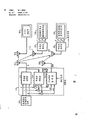
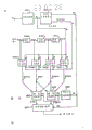
Fig. 1 is the block diagram of the two passage television signal transmission systems of working according to the present invention.
Fig. 1 a illustrates the work that is applicable to single channel encoder in the system shown in Figure 1.
Fig. 1 b is the block diagram that is applicable to single channel encoder in the system shown in Figure 1.
Fig. 1 c-1f, Fig. 2, Fig. 2 a and Fig. 3 a-3c illustrate the work of each parts of channel coder shown in Fig. 1 b.
Fig. 4 is for being applicable to shown in Fig. 1 b that every frame 1050 row (L/F) are interlaced to the converter block diagram that 525L/F lines by line scan in the single channel encoder.
Fig. 5 a and Fig. 5 b are for being applicable to the interleaved converter block diagram of lining by line scan in the single channel encoder shown in Fig. 1 b.
Fig. 6-8 is for being applicable to shown in Fig. 1 b the block diagram of edge strip-center signal separator and processor circuit in the single channel encoder.
Fig. 9 is the block diagram that is applicable to the NTSC encoder circuit of single channel encoder shown in Fig. 1 b.
Figure 10 and 10a-10c for explanation be used for single channel encoder shown in Fig. 1 b and single channel decoder shown in Figure 14 various vertical-block diagram and the form of termporal filter and level-vertical-termporal filter structure.
Figure 11 a and 11b are the block diagram that is applicable to the interior averager circuit of high-frequency frame of single channel encoder shown in Fig. 1 b.
Figure 12 and 12a-12d are applicable to shown in Fig. 1 b used any one time spreading device or the block diagram of time compression device circuit and the figure of explanation sort circuit work in the single channel encoder.
Figure 13 is the block diagram that is applicable to shown in Fig. 1 b amplitude compensation and quadrature modulation circuit in the single channel encoder.
Figure 14 is the block diagram that is applicable to single channel decoder of the present invention.
Figure 15 and Figure 16 are the block diagram that is applicable to the frame inner average device-difference engine circuit of single channel decoder shown in Figure 14.
Figure 17 is applicable to the quadrature demodulator of single channel decoder shown in Figure 14 and the block diagram of amplitude expander.
Figure 18 is the block diagram that is applicable to bright in the single channel decoder shown in Figure 14-chrominance signal split circuit.
Figure 19 is the block diagram that is applicable to the Y-I-Q format decoder circuit of single channel decoder shown in Figure 14.
Figure 19 a is the block diagram that is applicable to edge strip in the format decoder shown in Figure 19, central information splicer.
Figure 20 and Figure 21 are applicable to the block diagram that is interlaced to progressive scan converter in the circuit shown in Figure 14.
Figure 22 is the block diagram that is applicable to accessory channel luminance coding device in the accessory channel encoder of system shown in Figure 1.
Figure 22 a is the pixel map that can be used for illustrating circuit working shown in Figure 22.
Figure 23 is the block diagram that is applicable to shown in Fig. 1 b motion encoder and low pass filter in the single channel encoder.
Figure 24 is the block diagram that is applicable to accessory channel chroma coder in the accessory channel encoder of system shown in Figure 1.
Figure 24 a is the video field pattern that can be used for illustrating circuit working shown in Figure 24.
Figure 25 is used for carrying out for the auxiliary signal that accessory channel encoder shown in Figure 1 is produced the block diagram of the typical circuit of modulation and demodulation.
Figure 26 and Figure 27 are respectively and are applicable to that colourity and brightness in advanced compatible TV two channel decoder shown in Figure 1 augment the block diagram of decoding signals.
Figure 28 is applicable to that accessory channel luminance coding device shown in Figure 22 and brightness shown in Figure 27 augment the block diagram of motor message detector circuit in the decoding signals.
Figure 29 separates the block diagram of encoder for advanced compatible TV two passages shown in Figure 1.
Among the figure, the representative of single line arrow is used to transmit the bus of many bit parallels digital signal, or representative is used to transmit the signal path of analog signal or monobit digital signal.Bus or the signal type that signal path transmitted, clear and definite in addition under discussion.For the purpose of understanding, in some signal path, can omit compensation delay.The technical staff who is familiar with the digital signal processing circuit design knows where need such time-delay in concrete system.
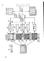
Fig. 1 is the block diagram that comprises two passage television signal transmission systems of the embodiment of the invention.Among Fig. 1, from source 110(for example, video camera) broadband widescreen high definition TV (HDTV) signal Y, I and Q are added on the transmitter 112.Signal Y comprises the luminance picture information that occupies frequency band between the 0-20MHz, and signal I and Q comprise the colourity image information that occupies frequency band between the 0-10MHz.
By that class single channel encoder 114 described in papers that the people writes such as Yi Sinadi above-mentioned and the application for patent, signal Y, I and Q are encoded.Then, utilize antenna 115 that encoded signals is launched.The antenna 120 that TV signal quilt that antenna 115 is launched and standard NTSC receiver 122 link receives, and in the width-screen EDTV receiver, quilt receives with the antenna 124 that wide screen extended definition television (EDTV) display 128 links.The width-screen EDTV receiver comprises that class single channel decoder described in paper that the people writes such as Yi Sinadi above-mentioned and the application for patent, be used for the signal decoding that receives become its formation, brightness and colourity picture content Y ', I ' and the Q ' of expanding articulation.Signal Y ', I ' and Q ' are presented on the width-screen EDTV display 128.
System shown in Figure 1 also comprises accessory channel encoder 142, in order to transmit, 142 encode for the signal of the difference of the original width-screen EDTV signal of representing width-screen EDTV signal (as shown in width-screen EDTV receiver 125 and 128) and source 110 to be provided.Differential signal is by output signal Y ', I ' that single channel decoder 140 provided and Q ' generation are provided corresponding signal Y, I that is provided from source 110 and the Q.Single channel decoder 140 can be identical with decoder 125.The auxiliary television signal that utilizes antenna 130 launching code devices 142 to provide.
The antenna 132 that the main channel signal that auxiliary channel signal that antenna 130 is launched and antenna 115 are launched is all linked with wide screen HDTV receiving system receives.This system comprises two channel decoder 134,134 are used for decoding for main channel signal and auxiliary channel signal, and be used for luminance and chrominance information decoded, its formation is carried out additive combination, be suitable for each component signal Y of wide screen HDTV that wide screen HDTV display unit 136 shows ", I " and Q " with generation.
Fig. 1 a by single channel encoder 114 the key diagram of employing signal coding technology.Encoder at first is reduced to the bandwidth of HDTV signal less than 6.0MHz, the HDTV signal is become the progressive-scan format of 525L/F from the interlacing scan format conversion of every frame 1050 row (L/F), then, formed signal encoding is become the NTSC compatible video with 4 component signals.One-component can produce the coloured image of standard the ratio of width to height, single-definition on tradition or standard ntsc television receiver 122; When three representation in components reappear on width-screen EDTV receiver 128 in addition, the enhancing of standard picture.These three are strengthened component and get up corresponding to the component combination of standard the ratio of width to height, single-definition image, make those three components and standard component occupy same frequency band, but, be hidden in actually or sensuously in the image that standard TV receiver 122 produced.
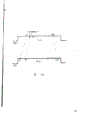
First component signal (that is standard component) be have 4: 3 the ratio of width to height of standard, 525L/F, 2: 1 interlace signals.This component comprises the central information of band limit HDTV signal, has carried out temporal extension to occupy the almost whole active line time for this central information.First component signal also comprises the horizontal low frequency information of edge strip, this low frequency information by time compression in a left side and right horizontal image overscan regions as 122 demonstrations that produce of standard NTSC receiver.In fact low frequency edge strip Information hiding is got up, the people be can't see, because standard NTSC receiver does not show this information.According to the following reason that will illustrate, before first component signal and second, third component signal were combined, first component signal that is higher than 1.5MHz for frequency carried out frame inner average.Fig. 2 illustrates the temporal extension and the time compression of first component signal.
The second component signal is 2: 1 interleaved signals of assisting, and wherein, has all carried out expansion to occupy effective half when capable for left and right edge strip high-frequency information.When in fact the edge strip information of having expanded like this, occupied second component signal whole effective capable.The generation of Fig. 3 c explanation second component signal.
Three component signal obtains from band limit HDTV signal, auxiliary 2: 1 interleaved signals.Three component signal is included in the horizontal luminance detail information of the high frequency that is about between the 5.0-6.0MHz.This information is carried out frequency move down, to occupy the frequency band between the 0-1.0MHz.
For second and three component signal all by frame inner average, amplitude compression, then, be used to modulate corresponding quadrature phase relevant, suppress alternated subcarrier signal ASC and ASC ', ASC and ASC ' have the frequency of the odd-multiple of half-line frequency, and are within the look passband of NTSC signal spectrum.Also have, the phase place of this alternated subcarrier signal changes 180 ° from one to next,, stipulates that one is 262 horizontal line cycles herein.Therefore, second of modulation and three-component any distortion of producing standard NTSC image all show as the complementary colour of frame frequency (30Hz) and change.People generally do not note this distortion, because human eye is for rapid, the complementary not too sensitivity that changes of the saturation level colour that runs into usually in TV signal.
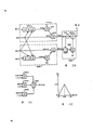
The 4th component signal is interlacing in 2: 1 " auxiliary " signal, and sort signal comprises vertically-time (V-T) luminance detail information, otherwise will lose in 525L/F lines by line scan the interleaved HDTV signal transformation of 525L/F.This signal helps the EDTV receiver to reformulate the information of losing in the motion scene, and reduces or eliminates unwanted flicker and mobile product in the wide-screen image of lining by line scan of generation on EDTV display 128 and HDTV display 136.Fig. 2 a explanation, how from 525L/F line by line scan and the 525L/F interleaved signal produce " auxiliary " signal.
By compression corresponding to the part of edge strip and expansion part corresponding to central information, make the 4th signal component be plotted on first component signal and frequency band limits to 750KHz.Signal with such formation comes modulated carrier signal, and this carrier signal is that quadrature phase is relevant for image carrier signal (being also referred to as video carrier signal), and makes up with three-component with modulated first, second.In traditional NTSC demonstration, the 4th component signal is hidden, because handle by this drafting, any distortion that may cause and first component all are space correlation.
Employing level-vertical-time (H-V-T) comb filter is partly carried out pre-filtering for the luminance signal of first component signal, with the luminance signal part of eliminating first component signal and potential the crosstalking between the carrier chrominance signal part.Also have, adopt the V-T comb filter, for first, second and three component signal carry out frame inner average eliminated substantially first component and second and three-component between V-T crosstalk, make receiver decoder 125 and 134 be easy to separate second with three component signal.Fig. 1 d and Fig. 1 e illustrate the frame inner average and the combination thereof of first, second and three component signal, to produce the NTSC signal of having encoded.
Though this is favourable in Code And Decode is handled,, the diagonal resolution of EDTV image shown in related comb filtering can reduce on the display 128 in above-mentioned treatment step.In spectrum analysis, the brightness signal Y that the single channel decoder is produced ' have up to ntsc video frequency spectrum traditional about 1.5MHz, also having with peak valley between the 1.5-6.0MHz alternately is the frequency spectrum (that is the signal spectrum of comb filtering) of feature.There is not the above frequency of 6.0MHz among the signal Y '.Also have, " auxiliary " signal band of the luminance signal of lining by line scan owing to being used for regenerating from the interleaved signal of emission is restricted to 750KHz, so, in the alternation between-line spacing of signal Y ', may there be the monochrome information between the 750KHz-20MHz.
Signal I and Q, (the colour information signal component of HDTV signal) all carried out frequency band limits before being separated between first and second component signals, be restricted to 600KHz.Because these signals as first and second component signal parts have been subjected to V-T filtering during frame inner average, so reproducing signal I ' and Q ' present and have the frequency spectrum that the peak valley of comb filtering signal characteristic replaces.
As mentioned above, cutting 525L/F progressive-scan signal Y ', I ' and the Q ' that single channel decoder 140 produced each 1050L/F interleaved signal Y, the I that are provided from wide screen HDTV source 110 of each differential signal △ Y, △ I and △ Q and the Q draws.Because exist vertical displacement between each the capable display position from each row display position of at least one interleaved signal Y, I and Q and corresponding progressive-scan signal Y ', I ' and Q ', so each differential signal △ Y, △ I and △ Q can have huge energy value on lower frequency.
Like this, in the frequency spectrum of scope, luminance difference sub-signal △ Y may have energy between 0-20MHz; In the spectral range between 0-10MHz, colour difference sub-signal △ I and △ Q may have energy.As described below, accessory channel encoder 142 is handled for signal △ Y, △ I and △ Q, has the auxiliary video signal of 6MHz bandwidth with generation.
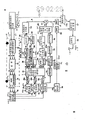
Fig. 1 b is the block diagram of expression wide screen HDTV source 110 and single channel signal encoder 114 details.The source 110 that is used for present embodiment of the present invention comprises wide screen 1050L/F interlacing scan video camera 10, utilizes the composite synchronizing signal CCPS and the frame frequency timing signal FT that are produced by studio timing generator 11, makes 10 to be synchronized with encoder 114.Be used in video camera 10 in the present embodiment of the present invention and produce the capable video information of every 525 row or every frame 1050.In each frame, each row and each line interlacing in next in one are got up.Though only show the camera source of 1050L/F, can imagine that the video tape recorder (VTR) of 1050L/F or the interleaved video camera of 1125L/F or VTR also can be as the sources of vision signal Y, I and Q.When adopting the source of 1125L/F, wish the line number of every frame to be reduced to 1050 by the image of shearing 1125L/F or by interpolation.
The video camera 10 that is used for this embodiment of the present invention is the video cameras of lining by line scan of 525L/F, and this video camera is adjusted to from one to another the vertically mobile hemistich of the image that it produced at interval.Be added to by frame frequency (30Hz) the square-wave signal FT that studio timing generator 11 is provided in the center control of video camera 10, realize that this image moves.In response to the signal FT with some values (for example, logical one), the video camera 10 that is used for the embodiment of the invention moves down half-line period to image.In response to other value of signal FT, video camera 10 returns to image initially without on the position of moving.The influence that the signal timing that video camera provides is not moved by image.
Red, green and blue (R, G and B) the primary colours output signal that video camera 10 is produced is added on the matrix 12, and 12 are transformed into brightness signal Y A to primary colour signal, and color difference signal IA and QA.Utilize A-D converter (ADC) 14 signal YA, IA and QA digitlization, utilize the clock signal of studio timing generator 11 8fsc that provides to control for 14.A-D converter 14 provides that to have sampling frequency be standard NTSC colour subcarrier signal frequency (f
Sc) 16 times wide screen HDTV signal Y, I and Q.
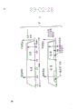
Be the summary of coding circuit shown in Fig. 1 b below.Signal Y, I and Q are added to 1050L/F to be interlaced on the 525L/F progressive scan converter 16.The output signal YF of scan converter 16, IF and QF are added on progressive-to-interlace scan converter 17a, 17b and the 17c, and 17a, 17b and 17c produce signal YF ', IF ' and QF ', and YF ', IF ' and QF ' are the interleaved signals of 525L/F.Scan converter 17c also produces a differential signal YT, and YT is used for producing " auxiliary " signal.As mentioned above, single channel decoder 125 and 140 utilizes auxiliary's signal to produce 525L/F progressive-scan signal Y ', I ' and Q ' from the 525L/F interleaved signal that receives.Carry out low-pass filtering for signal YF ', IF ' and QF ', then it is added on edge strip-center signal separator and the processor 18,18 these Signal Separation become corresponding edge strip and central information part, edge strip partly is separated into the high and low frequency component, the low frequency component of compression edge strip signal, expansion central information signal.Signal YE, the IE of central information expanded in representative with edge strip-center combination device 28 and signal YO, the IO and the QO that compress low frequency component of QE and representative edge strip combines, to produce signal YN, IN and QN.Signal YN, IN and QN are added on the NTSC encoder 31, and 31 output is the first component signal C/SL of above-mentioned single channel EDTV signal.
High fdrequency component YH, IH and the QH of separator and processor 18 edge strip that provides are added on the NTSC encoder 60, and circuit 62 carries out temporal extension for 60 output signal.The output signal of circuit 62 is second component signal ESH of above-mentioned single channel EDTV signal.
70 couples of signal YF ' from progressive-to-interlace scan converter 17C of filter carry out bandpass filtering, filter between the 5.0-6.0MHz; Modulator and low pass filter 72 carry out frequency shifts to it, move to 0-1.0MHz; Form encoder 74 carries out time compression to it, is compressed to consistent with the central information part of first component signal.The output signal of encoder 74 is three-components of EDTV signal.
Second and three component signal carried out frame inner average by circuit 64 and 76 respectively, to produce signal X and Z, 80 couples of signal X of circuit and Z carry out amplitude compression, and two relevant subcarrier signal ASC and ASC ' of quadrature phase are modulated with the Z signal with the X that has compressed.The output signal of circuit 80 is signal M.Circuit 38 carries out frame inner average for the first component signal C/SL, to produce signal N.Adder 40 combines signal M and N, to produce signal NTSCF.
Digital-to-analog converter (DAC) 54 and 53 is transformed into analog form to signal NTSCF and YTN respectively.Analog switch 58 is added to the composite synchronizing signal OCPS that studio timing generator 11 is produced on the signal NTSCF.Signal that switch 58 is provided and simulation " auxiliary " signal are added on radio frequency (RF) quadrature modulator 57 that produces first component TV signal.Utilize transmitter 55 this signal to be launched by antenna 115.
Be to the more detailed description of circuit shown in Fig. 1 b below.The output signal MAIN(master that 11 pairs of 1050L/F interlacing scans of studio timing generator video camera 10 and 525L/F interlacing scan have been encoded) provides composite synchronizing signal CCPS and DCPS.In addition, generator 11 also provides the clock signal 4f that is respectively NTSC colour subcarrier signal frequency 4,8 and 16 overtones bands
Sc, 8f
ScAnd 16f
Sc, data oscillator signal ASC, the ASC ' and the fc that have taken a sample, line frequency signal FS and H, rate signals FT.Provide switching signal SW signal OCPS to be inserted among the output signal MAIN that has encoded with control.Circuit 11 comprises the oscillator of traditional resonant crystal control, clocking 16f
ScCircuit 11 is from signal 16f
ScGeneration has relevant alternated subcarrier signal ASC and the ASC ' of quadrature phase of the frequency 3.1MHz of 395 times of as many as half-line frequencies, and the signal fc of the as many as 5MHz of frequency.For example, can have 16f by increasing by one
ScThe counter (not shown) of signal and count value is added to read-only memory (ROM) produces signal ASC, ASC ' and fc on the (not shown), programme to obtain representing the sampling value of these three signals for this ROM.Also have, this ROM can provide an output signal to be used to refer in every line time of a signal NTSCF interior predetermined pixel sample time (H) or one group of sample time (Fs) at interval.Can be added to one of signal ASC, ASC ' and fc on another counter (not shown), (this counter is programmed, with the signal FT that obtains to produce with frame frequency or field frequency, below with reference to Figure 11 a and Figure 11 b explanation.) exemplary device that produces various clocks and timing signal is 241277 in sequence number, is entitled as " about the vision signal synchro system of extended definition television system " (" Video Signal Synchroni
 Ation System as fov an Extended Difinition Television System ") the U.S. Patent application book in, done comparatively detailed description, draw now and be reference.
Wide screen HDTV signal Y, I that source 110 is provided and Q are added to 1050L/F and are interlaced on the 525L/F progressive scan converter 16, and 16 produce signal YF, IF and QF.Scan converter 16 is parts of single channel encoder 114.Fig. 4 illustrates the circuit block diagram that is applicable to scan converter 16.Circuit shown in Figure 4 is represented one of 3 passages (being respectively Y, I and Q) of scan converter 16.Other two passage (not shown) can be identical with this passage that illustrates, and just has not been described in detail.This circuit is being inserted in the sampling of 1050L/F interlacing scan input signal in the middle sampling value, and the sampling of the sampling of these interpolations and non-interpolation is combined, so that produce the progressive-scan signal of 525L/F on the output port of two parallel circuits 482.The interpolation sampling that scan converter 16 is produced is handled by Motion Adaptive and is drawn.In the image-region of representative motion, the interpolation sampling produces (that is, vertical average) from the sampling in a horizontal line time interval of interval.In the zone of rest image, the interpolation sampling is from producing (that is time average) the frame time sampling at interval at interval.
Among Fig. 4, the 1050L/F interleaved signal is added on the horizontal low pass filter 438.Filter 438 can be for 16f
ScThe sampling in succession of signal Y, I and Q averages, and can utilize signal 8f to produce
ScCarry out secondary sample and do not obscure the sampling of distortion.The signal that filter 438 is produced is added on 524 line periods (524H) delay unit 440, and 440 is first in 4 delay units that are connected in series.Other 3 delay units 442,444 and 446 provide corresponding 1H, 1H and 524H signal lag.The output signal of delay unit 442 is reference signals.Delay unit 440 and 444 output signal be leading respectively and time-delay 1H with respect to reference signal.Be added to a field duration of the output signal of input signal on the scan converter and delay unit 446 and time-delay 1050L/F interleaved signal leading respectively with respect to reference signal.
The output signal of delay unit 440 and 444 is added in the multiplexer 450 on the corresponding input port.The signal FT that utilizes studio timing generator 11 to be provided adjusts for multiplexer 450, and 450 successive fields at video camera 10 signal that provides are alternately provided in the time interval from the signal of delay unit 440 with from the signal of delay unit 444.The reference signal that signal that adder 458 and subtracter 456 are provided multiplexer 450 and delay unit 442 are provided combines.The output signal of adder 458 is vertical average signal VAVG, and the output signal of subtracter 456 is differential signal VDIFF.Signal VAVG and VDIFF representative is with respect to the delayed time signal addition and the combination of subtracting each other respectively of the reference signal of 525H and alternately delayed time with respect to input signal 524H and 526H of input signal.Utilize signal FT to control switching with the combined signal of reference signal, the image that is produced with tracking camera 10 moves.
In adder 460 and subtracter 462, combine being added to the input signal on the scan converter and the output signal of delay unit 446, with generation time average signal TAVG and time differential signal TDIFF respectively.Time average signal TAVG and time differential signal TDIFF always represent 1050H(1 frame time at interval at interval) the combination of signal.
Signal VDIFF and TDIFF are added on traditional motion detector 464, and the output signal 464 is added on traditional motion expander 466.Detector 464 can comprise for example comparator (not shown), and this comparator compares the relative amplitude of corresponding time difference sub-signal and vertical difference sub-signal (TDIFF and VDIFF).Also have, detector 464 can comprise horizontal low pass filter (not shown).Motion expander 466 can comprise the circuit (not shown), the motor message that sort circuit is provided detector 464 carries out thresholding control, and on level, vertical and time orientation, averaging through the signal of thresholding control so that the border extension of the image-region that comprises motion in the zone that does not comprise motion.Expand for motor message, to alleviate any boundary effect in the Motion Adaptive of any employing motor message is handled.Generally, when stagnant zone was handled as the moving region, the product that causes when the moving region is handled as stagnant zone lacked.
Signal M and the mark that (1-M) is complementation.The size of M be proportional to reference signal and leading and the video image internal field of the signal representative that lags between the level that moves.Like this, when moving between the field that has high level in certain part of shown image, in this a part of interpolated signal, the component that obtains with vertical average signal VAVG is bigger, and only obtains a small component from time average signal TAVG.In the static relatively zone of image, on the spot between the low place of motion level, this ratio is then opposite.
Exist or do not exist under the situation of moving between the field, switching between the vertical average and time average has produced interpolated signal, and this interpolated signal has All Time resolution and have whole vertical resolutions in the stationary part of this image in the motion parts of image.The inventor is definite, and this motor fitness is handled better than the result of pure temporal interpolation or the generation of pure vertical interpolation.
In two parallel circuits 474, calibrate for the output signal of adder 472 with coefficient 0.5, occupy the digital signal of identical amplitude range with generation and the signal on being added to scan converter 16.The reference signal that the two row output signals that provided of circuit 474 and delay unit 442 are provided is added on the adder 480 corresponding input ports, and 480 output port is coupled on the input port of two parallel circuits 482.The sampling value that is provided by video camera 10 has been provided for adder 480 and two parallel circuits 482, average with the interpolation sampling value of representing each row in the middle of the 1050L/F horizontally interlaced image.Like this, can think that the output signal that circuit 482 is provided is each average to consecutive line in the 1050L/F progressive-scan signal.The inventor is definite, and this is the good approximation for the 525L/F progressive-scan signal.
Referring to Fig. 1 b, 525L/F progressive-scan signal IF, QF that scan converter 16 is provided are added to respectively on different line by line scan progressive-interlace conversion device 17a, 17b and the 17c with YF.The circuit that is suitable for converter 17c is shown in Fig. 5 a, and the circuit that is suitable for converter 17a and 17b is shown in Fig. 5 b.
Scan converter shown in Fig. 5 a comprises by (525H) delay unit 510 and 512, the signal averager that adder 514 and two parallel circuits 516 form.The signal that signal averager provided is input signal Y F(or B), the signal A that provided with delay unit 512 average.These two field duration of two sigtnal intervals.In subtracter 518, from the signal X that delay unit 510 is provided, average signal is cut, to produce a differential signal YT.The video field signal of signal X representative between signal A and B.Signal X and YI are added to respectively on switch 520 fixed juncture separately.Utilization has the movable contact that square-wave signal FS that duty ratio 50%, frequency be substantially equal to NTSC prescribed by standard line frequency comes control switch 520.Signal Fs adjusts to sampling that capable signal X alternately is provided and the sampling of going signal YI to switch 520.In response to signal 8fsc, this sampling is write in the dual-ported memory 522; And in response to having the signal 4f that is substantially equal to look subcarrier frequency 4 overtones bands
Sc,, from memory 522, read concurrently as signal YF ' and YT.Signal YF ' is a 525L/F interlacing scan luminance signal.It is top referring to Fig. 2 a described " auxiliary " signal to utilize signal YT to produce.
Scan converter shown in Fig. 5 b comprises field compensation time-delay 530 and dual-ported memory 532.In response to corresponding signal 8f
ScAnd 4fsc, the time-delay of signal IF or QF sampling is stored into memory 532 neutralizations from 532, read.The output signal of memory 532 is 525L/F interleaved signal IF ' or QF ' that the orthochronous relation is arranged with signal YF '.
Referring to Fig. 1 b, signal IF ', QF ' and YF ' that corresponding scan converter 17a, 17b and 17c are provided are added on corresponding low pass filter 19a, 19b and the 19c.Filter 19a and 19b are compressed to 500KHz to the horizontal bandwidth of signal IF ' and QF '.Filter 19c is compressed to 5MHz to the horizontal bandwidth of signal YF '.Output signal IF that corresponding low pass filter 19a, 19b and 19c are provided ", QF " and YF " are added on edge strip-center signal separator and the processor 18.The details of processor 18 is shown in Fig. 6, Fig. 7 and Fig. 8.
Fig. 6 is the block diagram of processor 18-part, and 18 brightness signal Y F " is separated into and represents the signal YE of the center pixel of temporal extension, represent the signal YO and the signal YH that represents edge strip pixel high fdrequency component of the edge strip pixel of time compression.Adopt signal YE and YO to form first component of the EDTV signal of encoding, adopt signal YH to form the second component signal.
Among Fig. 6,610 couples of signal YF of low pass filter " carry out filtering, so that the signal that occupies frequency band between 0-700KHz YL to be provided.The signal YF of subtracter 612 from having delayed time " signal YL is cut, occupy the signal YHO of frequency band between 700KHz and the 5MHz with generation.The signal YF that has delayed time ", signal YHO and signal YL be added on the split circuit 616.The circuit 616 that to be described referring to Fig. 8 makes signal YF below " in pass through as signal YC corresponding to that part of picture centre information; And make among signal YHO and the YL corresponding to those parts of this image edge strip part and pass through as corresponding signal YH and YL '.As illustrated in fig. 2, time spreading device circuit 622 carries out temporal extension for signal YC, so that the YE of the signal with 4.2MHz bandwidth to be provided.Also as illustrated in fig. 2, circuit 628 carries out time compression for signal YL ', so that the YO of the signal with 4.2MHz bandwidth to be provided.Time spreading device 622 and time compression device 628 can utilize below and will understand referring to the circuit that Figure 12 and Figure 12 a-12d are described.
Circuit shown in Figure 7 is identical with circuit shown in Figure 6, the different just passbands of low pass filter 710 are 0-83KHz, rather than among filter 610(Fig. 6 corresponding with 710) 0-700KHz.
Fig. 8 is the block diagram of split circuit, and this circuit can be used as the separator 716 among Fig. 7, and is perhaps just as explained above, is available as the separator 616 among Fig. 6.Circuit shown in Figure 8 comprises 3 multiplexers 810,812 and 814, and each multiplexer is coupled to respectively on count comparator circuit 817,818 and 820.Each all is coupled together these count comparator circuit, so that accept the count value from counter 822.Signal 4f
ScCarry out clock control for counter 822.The signal H that studio timing generator 11 is provided resets counter 822, and H occurs once in each line period, with the position of indication first image sampling on each row.
In response to count value 1-84 and 671-754, count comparator 817 and 820 is adjusted corresponding multiplexer 810 and 814, makes 810 and 814 respectively by signal YHO and YL.In response to whole other count values, multiplexer 810 and 814 is by blanking signal BLK.Count comparator 818 is adjusted multiplexer 812 with same method, make 812 for the count value between the 75-680 by signal YF "; For other count value, pass through blanking signal.Oscillogram is illustrated in Fig. 8, reconstitutes the width-screen EDTV signal in order to help decoder, makes the pixel of center and edge strip overlapping, for example 10 samplings (following will the description).
As mentioned above, time spreading device 622,722 and time compression device 628,728 can utilize circuit for example shown in Figure 12 to understand.Circuit shown in Figure 12 utilizes 4 dual-ported memory 1216a-1216d, carries out temporal extension (by repeating some sampling) or time compression (by deleting some sampling) for a series of pixel values.Circuit shown in Figure 12 comprises that also a pair of peaking filter 1220,1222,1220 and 1222 amplifies for the high fdrequency component of signal that dual-ported memory provides; And 2 linear interpolaters 1230,1230 get up the signal combination of peaking, to produce the temporal extension or the vision signal of time compression.Peaking filter 1220 and 1222 compensated in 2 linear interpolations intrinsic low-pass filtering effect.Pixel counter 1210 and two programmable read-only memories (PROM) 1212,1225 are controlled circuit shown in Figure 12.By suitably programming for PROM1212 and 1225, the circuit among Figure 12 can be used for realizing the various expansions and the compressed coefficient.
During work, for example can be the signal YC that separator 616 is provided among Fig. 6 video input signals S(S) be added on dual-ported memory 1216a and 3 delay unit 1214a, the 1214b and 1214C that are connected in series.The output signal of delay unit 1214a, 1214b and 1214C is added on the input port of corresponding dual-ported memory 1216b, 1216c and 1216d.What pixel counter 1210 was provided for memory 1216a-1216d writes address signal M.Also signal M is added on the PROM1212,1212 produce be used for memory 1216a-1216d read address signal N and interpolation coefficient DX, DX is added on 2 linear interpolaters 1230 and the PROM1225.If adopt circuit shown in Figure 12 to carry out temporal extension, then PROM1212 programming is read address signal N with what produce that its nominal growth must be slower than signal M for a certain signal.This makes memory 1216a-1216d repeat some sampling value.On the other hand, if adopt this circuit to carry out time compression for a certain signal, the numerical value of then reading address signal N increases with the speed greater than signal M.This makes memory 1216a-1216d skip some sampling value.Illustrated as Figure 12 d, can be PROM 1225 programming, so that change the peakedness factor PX that is added on peaking filter 1220 and 1222 in response to different interpolation coefficients.
Figure 12 b illustrates the details of peaking filter 1220,1222 and 2 linear interpolaters 1230.Figure 12 c illustrates the details that is used for peaking filter 1220 high pass filters 1240; In peaking filter 1222, adopted an identical filter.
Referring to Fig. 1 b,, and separated and edge strip signal IO, QO and the YO of time compression are added on edge strip-center combination device 28 separating of being provided of processor 18 and central information signal IE, QE and the YE of temporal extension.Combiner 28 can comprise the counter (not shown), utilizes signal H to reset for this counter, utilizes signal 4f
ScCarry out clock for this counter.The counter value signal that this counter produced is added on the multiplexer (not shown), and this multiplexer combines Fig. 3 a illustrated signal YE and YO, to produce output signal YN.Combiner 28 comprises the circuit of same type, produces signal IN so that signal IE and IO combined, and signal QE and the QO generation signal QN that combines.
Signal YN, IN and QN that combiner 28 is provided are added on the NTSC encoder 31.Encoder 31 comprises level-vertical-time (HVT) filter 34,34 handle for signal YN by the comb filter transfer function, and this transfer function is may removing with some spectrum component that modulated color sub-carrier signal and modulated alternated subcarrier blurring get up in the luminance signal.The output signal of HVT filter 34 is signal YP.Color difference signal IN and QN are added on the quadrature modulator 30, in response to clock signal 4f
Sc, 30 produce NTSC carrier chrominance signal CN.Signal CN is added to vertically-time (VT) filter 32 on, 32 carry out comb filtering for signal CN, removing corresponding to modulated alternated subcarrier signal with corresponding to the spectrum component of high-frequency brightness signal.The output signal of filter 32 is signal CP.Signal combiner 36 gets up signal CP and YP additive combination, to produce the first component signal C/SL of the EDTV signal of having encoded.
Fig. 9 is the block diagram that more details in the NTSC encoder 31 are shown.Among Fig. 9, a pair of latch 910 and 912 is in response to clock signal 2f
ScAnd 4f
Sc, signal IN and QN time division multiplexing are become the sampled signal that I and Q replace.Circle on latch 910 inputs shows 910 in response to clock signal 2f
ScThe paraphase value.Latch 910 and 912 signals that provided are added on second pair of latch 914 and 916, and 914 and 916 change the right polarity of respectively alternately taking a sample as shown in Figure 9 to produce signal CN.Signal CN is added on the VT band pass filter 32.Studio timing generator 11 provides signal 4f
Sc, 2f
ScAnd f
Sc
Figure 10 is the block diagram of finite impulse response (FIR) (FIR) filter that is applicable to filter 32.Filter shown in Figure 10 adopts sampling from 4 successive fields to produce its output signal.Corresponding filter coefficient value a1-a9 is multiply by in each tap in 9 taps of filter.Figure 10 a is for being used for constituting the coefficient value form that resembles VT band pass filter 32 or resemble the filter shown in Figure 10 the VT band stop filter that for example is used for HVT band stop filter 34.
Figure 10 b is the filter block diagram that is applicable to HVT band stop filter 34.In fact, filter 34 has the flat frequency response characteristic at 0-1.5MHz; At 1.5-4.2MHz, has the comb frequencies response characteristic.The reset of pectination characteristic in stoping basically on each component position that in modulated carrier chrominance signal, may appear as the signal YN that crosstalks.Among Figure 10 b, signal YN is added on the horizontal low pass filter 1020,1020 have the passband of 0-1.5MHz.From the signal YV that compensation delay unit 1022 is provided, the output signal of filter 1020 is cut to produce the luminance signal of high-pass filtering.The luminance signal of high-pass filtering has been added to for example top referring on Figure 10 and the described VT band stop filter 1021 of Figure 10 a.The output signal of VT band stop filter 1021 with as compensation delay unit 1024 provide that the luminance signal of low-pass filtering combines, to produce output signal YP.As shown in Figure 9, the signal CP additive combination that combiner 36 is provided signal YP and VT band pass filter 32 is to produce the first component signal C/SL.
Referring to Fig. 1 b, edge strip-center signal separator and processor 18 signal IH, QH and YH that provided, that represent edge strip high fdrequency component in the wide-screen image are added on the NTSC encoder 60.Encoder 60 can be identical with above-mentioned NTSC encoder 31.The output signal NTSCH of encoder 60 is added on the time spreading device circuit 62,62 expand to produce signal ESH for the edge strip high-frequency signal shown in Fig. 3 c like that, and ESH occupies in the line period corresponding to signal C/SL central information that portion of time partly.Time spreading device 62 is understood referring to Figure 12 and the described circuit of Figure 12 a-12d above for example can utilizing.Signal ESH is the second component signal of width-screen EDTV signal.
The brightness signal Y F ' that progressive-to-interlace scan converter 17c is provided is added on the band pass filter 70, and 70 lead to the frequency of 5.0-6.0MHz scope on amplitude modulator and the low pass filter 72.Can be that the modulator 72 of traditional design makes signal that band pass filter 70 provided and has the data sinusoidal signal fc that as many as 5MHz frequency taken a sample and mix.Studio timing generator 11 provides signal fc.Circuit 72 comprises low pass filter, and this low pass filter removes baseband signal more than the 1.0MHz and modulation signal.Circuit 72 performed work are that high-frequency brightness information is carried out frequency shifts basically, move to the 0-1.0MHz frequency band from 5.0-6.0MHz.The signal that modulator and low pass filter 72 are provided is added on the form encoder 74, and 74 pairs of these signals carry out time compression, to occupy in the line period that portion of time corresponding to signal C/SL central information part.
Utilize corresponding frame inner average circuit 38,64 and 76, the signal that the signal C/SL that is provided for NTSC encoder 31, the signal ESH that time spreading device 62 is provided and form encoder 74 are provided carries out frame inner average.It is all identical that this frame inner average is handled each field signal that makes among two of arbitrary frame.To make the EDTV decoder be easy to the method that the various component signals in the width-screen EDTV signal are separated in order utilizing, second, third component signal and first component signal to be combined, it is important that this frame inner average is handled.
As mentioned above, only just carry out frame inner average for being higher than 1.5MHz and the frequency component in the central information zone among the signal C/SL.Be lower than 1.5MHz and the component in the edge strip zone does not carry out frame inner average for frequency, to keep reconstituting the vertical and time detail in the image.Figure 11 b is the circuit block diagram that is applicable to averager 38 in the high-frequency frame.Among Figure 11 b, input signal IN(in this example, be signal C/SL) on (262H) delay unit 1120 and 1122 of being added to that pair of series connects.The output signal Y1+C1 of delay unit 1120 is added on the input port of average circuit 1128, another input port of connection 1128 is to accept the output signal of input signal Y 2+C2 or delay unit 1122 by multiplexer 1125.The rate signals Fs that utilization is added on the 1125 control input end mouths adjusts for multiplexer 1125, makes 1125 to provide signal Y2+C2 in a field interval of frame, and the output signal of delay unit 1122 is provided in another field interval of this frame.Multiplexer 1125 always provides the signal Y1+C1 that provided with delay unit 1120 in same frame.
The circuit that is applicable to frame inner average device 64 or 76 is shown in Figure 11 a.Among Figure 11 a, signal IN(in this example, be signal ESH) be added on the delay unit 1110 and 1112 of pair of series connection.The output signal Y1+C1 of delay unit 1110 is added on the input port of average circuit 1118, the output signal of input signal IN or delay unit 1112 is added on another input port of circuit 1118 by multiplexer 1115.Utilize field frequency (60Hz) switching signal Fs that multiplexer 1115 is adjusted, make 1115 in the input signal alternate fields time interval output signal by signal IN and delay unit 1112 alternately.The signal Y1+C1 that signal that multiplexer 1115 is provided and delay unit 1110 are provided is always in same frame time interval.Average circuit 1118 is calibrated its each input signal with coefficient 1/2 and formed signal is added together, to produce the output signal of frame inner average.
Referring to Fig. 1 b, the output signal of averager in the high-frequency frame 38 is added on the input port of adder 40.Utilize modulator 80, carry out amplitude compression for the output signal X and the Z of corresponding frame inner average device 64 and 76, and modulate for quadrature phase relevant alternated subcarrier signal ASC and ASC ' with Z, to produce signal M with the X that has compressed.Signal M is added on second input port of adder 40.The output signal NTSCF of adder 40 is combinations of first, second and three component signal of width-screen EDTV signal.Signal NTSCF is added on the digital-to-analog converter (DAC) 54.
Figure 13 is the circuit block diagram that is applicable to modulator 80.Among Figure 13, signal X and Z that corresponding frame inner average device 64 and 76 is provided are added on corresponding PROM1310 and 1312.Programme in PROM1310 and 1312 each with the amplitude compression function, near PROM1312, an example of amplitude compression function is described by illustrated input-output function.The output signal of corresponding PROM1310 and 1312 is added to respectively on multiplier 1314 and the 1316 corresponding first input end mouths.Second input port that connects multiplier 1314 is to accept alternation subcarrier signal ASC ', and second input port that connects multiplier 1316 is to accept alternation subcarrier signal ASC.Studio timing generator 11 provides signal ASC and ASC '.Adder 1320 adds multiplier 1314 and 1316 output signal is in the same place, to produce the output signal M of quadrature modulation.
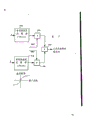
Referring to Fig. 1 b, the frame difference signal YT that progressive-to-interlace scan converter 17c is provided is added on the form encoder 78.Form encoder 78 can comprise circuit aforementioned and Figure 12 and the relevant type of Figure 12 a-12d.Encoder 78 is partly expanded for the central information of signal YT, partly compresses for its edge strip, and is illustrated as Fig. 1 f.The signal that form encoder 78 is provided is added on motion encoder and the low pass filter 79.Typical circuit as motion encoder and low pass filter 79 is shown in Figure 23.
The motion encoder of circuit 79 is for the change of the signal YT of representative image motion, is just or negative according to this signal respectively, with+10IRE(Institute of Radio Engineers) unit or-10IRE unit changes.When existing the significant noise of value in the transmission channel between transmitter and the receiver, this conversion has strengthened in the receiver performance of decoded signal YT.The application of this motion encoded " auxiliary " signal will be described referring to Figure 22 and Figure 27 below.
In the circuit shown in Figure 23, the signal that form encoder 78 is provided is added on the input port of adder 2368 and comparator 2364.Comparator 2364 produces output signals, and the signal that this output signal indication form encoder 78 is provided just is, bear, or numerical value is zero.The signal that utilizes comparator 2364 to be produced is adjusted for multiplexer 2366, makes 2366 just to be, to be negative or numerical value when being zero when " auxiliary " signal, respectively by represent 10IRE unit ,-digital value of 10IRE unit or 0IRE unit.The signal that multiplexer 2366 is provided is added on second input port of adder 2368.The output signal of adder 2368 is added on the low pass filter 2378 with 0-750KHz passband.The output signal of filter 2378 is output signal YTN of circuit 79.Signal YTN is added to shown in Fig. 1 b on the digital-to-analog converter DAC53.
Digital-to-analog converter 53 and 54 produces the analog form of signal YTN and NTSCF respectively.The signal that digital-to-analog converter 54 is produced is added on the analog switch 58, the signal SW that utilizes studio timing generator 11 to be provided controls for 58, and 58 composite synchronizing signal OCPS(OCPS are also provided by generator 11) be inserted in the level and vertical blanking time interval of simulation NTSCF signal.Though signal OCPS illustrates as analog signal,, expectation can be adopted digital signal OCPS.In this example, can replace analog switch 58 with the multiplexer of two traditional inputs, this multiplexer will be between adder 40 and digital-to-analog converter 54.
The output signal of switch 58 is added on the input of radio frequency (RF) quadrature modulator 57.Another input that connects modulator 57, to accept auxiliary's signal, i.e. the analog form of the digital-to-analog converter 53 signal YTN that provides.Modulator 57 produces vestigial sideband television signal MAIN, and MAIN has the signal NTSCF as common phase component, and has the auxiliary signal as its quadrature phase component.The signal that modulator 57 is provided is added on the transmitter 55 that transmits by antenna 115.
As shown in Figure 1, the signal MAIN that single channel encoder 114 is provided is added on the single channel decoder 140.The circuit that is applicable to decoder 140 is shown in Figure 14.Summarize its work, decoder shown in Figure 14 carries out demodulation for signal MAIN, to recover its in-phase component NTSCF and quadrature phase component YTN respectively.Handle to recover first, second and three component signal for signal NTSCF.Further decode for these signals, and suitably compress or expand, also make up, to produce brightness signal Y F ', color difference signal IF ' and QF ', these signals are the 525L/F interleaved signal.YTN also decodes for auxiliary signal, and is used for a signal YF ' and is transformed into the 525L/F progressive-scan signal.Under situation about not helping, color difference signal IF ' and QF ' are transformed into progressive-scan format from auxiliary's signal.At last, progressive-scan signal YF, IF and QF are transformed into analog signal Y ', I ' and Q '.
Among Figure 14, signal MAIN is added on the input unit 1422.Input unit 1422 comprises radio frequency (RF) tuner and amplifier circuit, is used for drawing the homophase that receives vision signal and the synchronous vision demodulator of quadrature phase modulation product, and A-D converter (ADC).The in-phase modulation component of the signal NTSCF representation signal MAIN that A-D converter provided in the input unit 1422; Signal YTN represents the modulation product of quadrature phase.
Signal NTSCF is added on synchronizing signal separation and the clock generating circuit 1423.Circuit 1423 comprises from signal NTSCH to be separated horizontal-drive signal HS and vertical synchronizing signal VS respectively, and signal HS and VS are combined to produce the traditional circuit of composite synchronizing signal CS.Circuit 1423 also comprises producing to have corresponding frequencies 4f
ScAnd 8f
ScThe conventional phase locked loops (PLL) of (among the signal NTSCH 4 times and 8 times of burst signal component frequency f sc) two clock signal C K4 and CK8.Circuit 1423 produces from signal CK4 has 395 times that are substantially equal to the 3.1MHz(half-line frequency) the relevant alternated subcarrier signal ASC and the ASC ' of quadrature phase of frequency, and have the signal fc that is substantially equal to the 5MHz frequency.For example can be by the count value of counter (not shown) being increased progressively with signal CK4, and this count value is added to compiled journey with on the read-only memory (ROM) that representation signal ASC, ASC ' and fc sampling value are provided, produce this three signal ASC, ASC ' and fc.Also have, this ROM can provide indication at every line time of signal NTSCF output signal H of interior at interval predetermined pixel sample time.Can be added to this signal H and compile journey and below will be described, on another counter (not shown) of the such signal of FS that occurs with frame frequency or field frequency referring to Figure 15 and Figure 16 for example to provide.Be used in receiver producing sequence number that the typical circuit of various clocks and timing signal mentions in the above and be in 241277 the U.S. Patent application book and done comparatively detailed description.
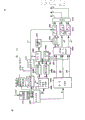
The signal NTSCF that input unit 1422 is provided also is added on the frame inner average device one difference engine circuit 1424.Circuit 1424 produces average pixel value and pixel difference value for the respective pixel that constitutes among two an of frame.Average pixel value is the output signal N corresponding to EDTV signal first component, and the pixel difference value is corresponding to width-screen EDTV signal modulated second and three-component output signal M.Figure 15 and Figure 16 illustrate to be suitable for to be the circuit block diagram of frame inner average device one difference engine 1424.Figure 15 illustrates in first field interval of a frame, the work of circuit 1424; Figure 16 illustrates in second field interval of a frame, the work of circuit 1424.
Among Figure 15 and Figure 16, signal NTSCF is added on two delay units that are connected in series 1520 and 1522 as input signal IN.Each delay unit 1520 and 1522 all provides the time-delay that is substantially equal to a field duration (262 row).Respectively the output signal of signal IN and delay unit 1522 is added on the different input ports of multiplexer 1525.The rate signals FS that utilizes timing generator 1423 to be provided adjusts for multiplexer 1525, make 1525 the alternate fields of signal MAIN in the time interval by two input signal.The signal that signal that multiplexer 1525 is provided and delay unit 1520 are provided is always in same frame.The signal that signal that delay unit 1520 is provided and multiplexer 1525 are provided is added on the average circuit 1528.
Referring to Figure 14, the signal M that circuit 1424 is provided is added on quadrature demodulator and the amplitude expander circuit 1426.Circuit 1426 carries out quadrature demodulation for signal M, and carries out the amplitude expansion for the signal of formed homophase and quadrature phase, to recover in the EDTV signal corresponding second and three-component.Figure 17 is the circuit block diagram that is applicable to quadrature modulator and amplitude expander circuit 1426.
Among Figure 17, in corresponding multiplier 1710 and 1712, signal M be multiply by signal ASC and ASC '.The output signal of multiplier 1710 and 1712 is added on corresponding low pass filter 1713 and 1715, and 1713 and 1715 remove signal M and any high frequency modulated component basically.The output signal of filter 1713 and 1715 is added on corresponding programmable read-only memory (PROM) 1714 and 1716.Being that the amplitude spread function of the inverse of amplitude compression function is programmed for PROM 1714 and 1716; This amplitude compression function is used for encoder, so that second and three-component in the compatible composite signal stashed psychologically in spirit.The output signal X of PROM 1714 is decoded second component signal, i.e. the component of extended high frequency of edge strip signal.The output signal Z of PROM 1716 is decoded three component signal, i.e. the high-frequency brightness signal of the frequency displacement component of broadband width-screen EDTV signal.
Referring to Figure 14, signal X is added on the edge strip compressor circuit 1428, effective inverting is carried out in 1428 expansions of the edge strip data being carried out for encoder circuit.This operation has produced edge strip signal high frequency signal NTSCH, and this high fdrequency component has been recovered the orthochronous relation of the time compression central information that produces with Y-I-Q form encoder 1444, will be described referring to Figure 19 below.Above can utilizing, compressor circuit 1428 understands referring to the circuit of Figure 12 and Figure 12 type that a-12d describes.
Adopt the compressed coefficient 0.22, the edge strip of the compression data from the second component signal X of EDTV signal produce signal NTSCH.Signal NTSCH is added on the bright color separating circuit 1440, and 1440 separate the luminance component of signal NTSCH (YH) and chromatic component, and carry out demodulation to obtain two color difference signal components (IH and QH) for chroma signal component.Signal YH, IH and QH bright with utilizing-Y/C separating circuit 1442 is added on the Y-I-Q format decoder 1444 from signal YN, IN and the QN that the first component signal N produces.Circuit 1440 can be identical with 1442, and typical circuit is shown in Figure 18.
Among Figure 18, signal N or signal NTSCH are added on band pass filter 1810 and the delay unit 1812,1812 compensation are by the processing time-delay of filter 1810.The filter 1810 that is used for present embodiment of the present invention is level-vertical-time (H-V-T) band pass filter.The typical circuit of HVT filter 1810 is shown in Figure 10 c.This filter comprises the horizontal band pass filter 1030 with passband 3-4.2MHz, and the VT band pass filter 1031 that utilizes coefficient value defined shown in finite impulse response (FIR) FTR filter shown in Figure 10 and Figure 10 a.The carrier chrominance signal of the output signal of filter 1810 for having separated.This signal is added on the subtrahend input port of subtracter 1814, the minuend input port of connection 1814 is to accept the signal that compensation delay unit 1812 is provided.The output signal of subtracter 1814 is luminance component signal YN or YH.
Can be expressed as the carrier chrominance signal that filter 1810 is produced a sequence of sampling value, I, Q ,-I ,-Q, I, Q ... herein, I and Q represent the sampling of I and Q color difference signal, the symbolic representation sampling phase of sampling, not necessarily Qu Yang polarity.This carrier chrominance signal is added on first and second latchs 1815 and 1816.The I phase clock signal ICK that latch 1815 is provided in response to clock generating circuit among Figure 14 1423 is to keep representing the carrier chrominance signal sampling value of I color difference signal component in the carrier chrominance signal.Latch 1816 is 1822 that provided in response to phase inverter, the paraphase form of signal ICK, to keep representing the sampling value of Q color difference signal component in the carrier chrominance signal.Latch 1815 and 1816 output signals that provided are added on the complementary circuit 1818 and 1820 of corresponding Z.The signal that utilizes frequency divider 1824 to be provided is controlled for circuit 1818 and 1820, so that to the alternately supplement of sampled data of I and Q color difference signal.Circuit 1818 and 1820 signals that provided are respectively demodulated signal IN or IH and QN or QH.
As mentioned above, signal YH, YN, IH, IN, QH and QN are added on the Y-I-Q form encoder 1444, in 1444, these signal combination are got up to form wide screen signaling YF
o', IF ' and QF '.The typical circuit that is available as form encoder 1444 is shown in Figure 19.Among Figure 19, YUV YN, the IN of first component and QN are added on edge strip-central information splitter circuit 1940.The circuit 1940 that for example can comprise separator (not shown) and pixel counter (not shown) is gone up each row the pixel value of representing edge strip signal low frequency component and is represented the sampling of central information signal to separate.In present embodiment of the present invention, pixel 1-14 and 741-754 representative edge bars, and pixel 15-740 represents the central information signal.
Utilize splicer 1960 that edge strip that has recovered and central information signal are reconfigured, with the luminance signal (YF ') that produces wide screen and color difference signal (IF ' and QF ').Be suitable for to the circuit of splicer 1960 and be shown in Figure 19 a.Among Figure 19 a, show the splicer that comprises network 1910,1910 are used for the signal YC of brightness central information is stitched together with the signal YS of two edge strips respectively, to produce wide screen brightness signal Y F
0'.Also have, Figure 19 a illustrates I signal splicer 1920 and Q signal splicer 1930,1920,1930 and has identical structure and work with the top Y-signal splicer that has illustrated.
In coding work, deliberately make the signal overlap of central information and edge strip, for example insecure sampling value that may occur in the processing is being expanded and compressed to 10 sampling points on the border in edge strip and central information zone, with compensation.If edge strip and central information do not have the overlapping region, then insecure sampling will be close together each other, will see seam in the image of reorganization.Find that the overlapping region of 10 sampling points is enough to nearly 5 insecure sampling values of compensation.
Among Figure 19 a, before being added to signal YS on the adder 1915, multiplier 1911 multiply by weighting function W to edge strip signal YS in the overlapping region, illustrated as relevant waveform.Similarly, before being added to signal YC on the adder 1915, multiplier 1912 multiply by complementary weighting function (1-W) to central information signal YC in the overlapping region, illustrated as relevant waveform.In the overlapping region, these weighting functions are rendered as the linear ramp type characteristic and have numerical value between the 0-1.These weighting functions for example can utilize for ROM(not shown) combination of carrying out the sampling counter (not shown) of addressing realizes that this ROM comprises the sampling value of representing weighting function.The wide screen brightness signal Y F of the output signal of adder 1915 for having spliced
0'.
Referring to Figure 14, the signal Z that quadrature demodulator and amplitude expander 1426 are provided is added on the time spreading device 1430.Understand time spreading device 1430,1430 referring to Figure 12 and the described circuit of Figure 12 a-12d above for example can utilizing and expand, to occupy line time whole effective video part at interval for the three component signal Z of width-screen EDTV signal.The signal that time spreading device 1430 is provided is added on the amplitude modulator 1432.
The signal fc that signal that amplitude modulator 1432 is provided time spreading device 1430 and clock generating circuit 1423 are provided multiplies each other, so that high-frequency brightness signal is returned to its original frequency band.The high-frequency brightness signal that modulator 1432 is provided is added to stop and is lower than on the high pass filter 1434 of 5MHz frequency.This filter is provided by the base band component of modulator 1432 signal that provides and any low frequency modulations component.The output signal of high pass filter 1434 is added on the input of adder 1436, connects another input acknowledge(ment) signal YF of 1436
0'.Adder 1436 is high fdrequency component of luminance signal (between the 5.0-6.0MHz) and wide screen brightness signal Y F
0' combine, to produce wide screen brightness signal Y F '.
Be added on format decoder 1460 and the nucleation circuit 1458 by the signal YTN that input unit 1422 is provided, from signal YTN, " auxiliary " signal YT recovered out.Format decoder 1460 is partly expanded and its edge strip is partly compressed for the central information of signal YTN, is added to improved " auxiliary " signal on the nucleation circuit 1458 with generation.Circuit 1458 have-the 10IRE unit value-+improvement " auxiliary " signal between the 10IRE unit value changes to 0IRE unit.Also have, circuit 1458 cuts 10IRE unit from the value of value greater than any sampling value of 10IRE unit of signal YTN.This inverting the performed level of encoder move, and, eliminated the little clutter (less than 10IRE unit) of any amplitude of improvement " auxiliary " signal of controlling oneself.The output signal of nucleation circuit 1458 is added to below will be referring to being interlaced on the progressive scan converter 1450 that Figure 21 is described.
Signal YF ', IF ' and QF ' be added to be interlaced to accordingly on progressive scan converter 1450,1452 and 1454.Figure 20 and Figure 21 are respectively exemplary scanning converter 1452(or 1454) and 1450 block diagram.Scan converter shown in Figure 20 comprises adder 2014 and two parallel circuits 2016,2014 and 2016 couples of input signal B(promptly, IF ' or QF ') the signal A that provided with delay unit 2012 averages to produce signal X.Signal A is delayed time a frame time at interval with respect to signal B.The signal C that signal X and delay unit 2010 are provided is added on corresponding dual-ported memory 2018 and 2020.In response to signal CK4, sampling value write memory 2018 and 2020; In response to signal CK8, from memory 2018 and 2020, read.The output signal of memory 2018 and 2020 is added on the respective input mouth of multiplexer 2022.By multiplexer 2022 row of signal X and the row of signal C are replaced to form progressive-scan signal IF or the QF of 525L/F.
Scan converter shown in Figure 21 comprises whole circuit shown in Figure 20, and comprises that adder 2118,2118 is added to the auxiliary signals of reappearing on the average signal X of frame, to form signal X '.Signal YT represents the approximation of each row sampling value frame inner average and the difference between the actual sampling value as previously mentioned.Like this, the sampling of row in the middle of signal X ' represents has been done correction for the mistake in these samplings in the average treatment that produces these samplings.The output signal of scan converter shown in Figure 21 is the progressive-scan signal YF of 525L/F.
Referring to Figure 14, signal YF, IF and QF are added on the digital-to-analog converter circuit 1462 that produces corresponding analog signal Y ', I ' and Q '.As shown in Figure 1, from wide bandwidth screen 1050L/F interleaved signal Y, I and Q, signal Y ', I ' and Q ' are cut, to produce broadband differential signals △ Y, △ I and △ Q.These broadband differential signals are added on the accessory channel encoder 142.
As mentioned above, referring to Fig. 1, broadband differential signals △ Y has the frequency spectrum that scope is 0-20MHz, and signal △ I and △ Q have the frequency spectrum that scope is 0-10MHz.Auxiliary signal encoder 142 is encoded for these signals, weaves into the signal AUX with 6MHz bandwidth.Also have, signal AUX can comprise digital audio and video signals.Encoder 142 adopts circuit separately to luminance difference sub-signal △ Y, and two color difference sub-signal △ I and △ Q encode.Be used for being shown in Figure 22, be used for being shown in Figure 24 for the circuit that △ I and △ Q encode for the circuit that △ Y encodes.
Among Figure 22, by means of the band pass filter 2248 of the band pass filter 2246 of the low pass filter 2244 of 0-6MHz, 6-12MHz and 12-18MHz signal △ Y division becoming component " A ", " B " and " C ".Frequency between the 18-20MHz does not comprise energy substantially and does not launch.Like this, component A is rendered as the frequency spectrum of 0-6MHz, the frequency spectrum that component B is rendered as 6-12MHz, the frequency spectrum that component C is rendered as 12-18MHz.Component A is coupled on the input terminal of switch S.
Utilize corresponding frequency mixer and low-pass filter circuit 2250 and 2252, carry out down-conversion to occupy the frequency band between the 0-6MHz for component B and C.Utilize corresponding row averager 2254 and 2256 for the row of the component B of down-conversion and C to averaging.Average row is coupled on each different input terminal of the switch S 2 of working with 15KHz speed (line frequency 32KHz partly).The output signal of switch S 2 comprises that B component signal average, that replace is capable and the C component signal is capable.For carried out on average this of B and C component with alternately reduced the vertical bandwidth of the horizontal high fdrequency component of B and C component signal representative.Because the monochrome information of the alternate row of switch S 2 output signals representative in 6-12MHz and 12-18MHz frequency band is so this efficient in operation ground merges to the information in the 6-18MHz frequency band in the 0-6MHz frequency band.The lead-out terminal of switch S 2 is coupled on second input terminal of switch S 1.
Though a lot of motion detectors are known,, advantageously adopted improved " auxiliary " signal (the 4th component of above-mentioned width-screen EDTV signal) to draw the motion index signal that then will describe.As shown in Figure 1, utilize single channel decoder 140 to offer accessory channel encoder 142 to improved " auxiliary " signal.This signal is to produce referring to the described method of Figure 23.
Figure 28 explanation is used to provide the interface of " auxiliary " signal between single channel decoder 140 and accessory channel encoder.Among Figure 28, improvement " auxiliary " signal that form encoder 1460 is provided is added on the nucleation circuit 1458 (as shown in figure 14) and is added on the motion detector 2260.For improvement " auxiliary " signal value between 10IRE unit and (10) IRE unit, the signal that detector provided is designated as and does not move; And for " auxiliary " signal value outside this scope, the signal that detector provided is designated as in the handled image and exists intraframe motion.
Figure 24 can be used for the circuit block diagram of encoding for differential signal △ I and △ Q.Circuit shown in Figure 24 has reduced the level and the vertical bandwidth of △ I and each signal of △ Q, carries out time-division multiplex for △ I that has compressed bandwidth and △ Q signal, then, carries out time compression for formed signal.The signal of time compression division becoming high and low frequency component, alternately provide the high and low frequency component to form signal CA with the speed of field frequency.The signal YA that is provided for signal CA and accessory channel luminance coding device carries out time-division multiplex, has the vision signal of the illustrated multiplexed component format of Figure 24 a with generation.
More precisely, among Figure 24, signal △ I and △ Q are added on corresponding 2.4MHz low pass filter 2410 and 2416,2410 and 2416 reduce the resolution of △ I and △ Q signal.Filter 2410 and 2416 signals that provide process to be with and to limit are added on corresponding capable average circuit 2412 and 2418. Circuit 2412 and 2418 averages for the corresponding sampling value from consecutive line among corresponding signal △ I and the △ Q.Average circuit 2412 and 2418 signals that provided are added on the respective input mouth of line frequency multiplexer 2414.Digital audio and video signals shown in Figure 1 is inserted into, and be included among the signal YA/CA.
Figure 25 is applicable to the rf modulations of system shown in Figure 1 and the block diagram of demodulator circuit.In this circuit, 6MHz signal YA/CA is added on the capable separator 2510,2510 expander circuits of axle when the line time of signal YA/CA even-numbered offered at interval 2512 offer time spreading device circuit 2516 at interval to the line time of odd-numbered.Circuit 2512 and 2516 carries out temporal extension with coefficient 2 for the signal that is added on its input port, makes each row of input signal go corresponding to two of output signal, and occupies the frequency band between the 0-3MHz.Time spreading device circuit 2512 and 2516 signals that provided are added on the modulator 2514, and 2514 can carry out double-sideband modulation (DSM) for the relevant carrier signal of pair of orthogonal phase place with two input signals; Perhaps carry out Double SSB modulation (DSSM) for a carrier signal,, keep upper sideband, and, retain sideband for another input signal for an input signal with each input signal.The signal that modulator 2514 is provided produces same passage interference hardly for existing ground broadcast television signal, because carrier wave is placed in the center of transmission spectrum, even occur a bit disturbing, can as the interference that noisy conventional television signal produced, not intrinsic also.The output signal of modulator 2514 is signal AUX, by antenna 130 signal AUX is transmitted to two channel decoder 134.Decoder 134 comes received signal AUX by antenna 132.
Radio-frequency (RF) demodulator 2522 in two channel decoder 134 for two the signal of temporal extension carry out demodulation, and the result is added on time compression device circuit 2524 and 2526. Circuit 2524 and 2526 carries out time compression with coefficient 1/2 for respective input signals, and formed signal is offered capable multiplexer 2528.Multiplexer 2528 alternately provides the signal that is added on two input port in the line time interval that replaces, with restoring signal YA/CA.
Figure 29 is the block diagram of typical two channel decoder 134.Among Figure 29, antenna line frequency multiplexer 2414 provided at interval at the line time that replaces go the average △ I and the sampling of △ Q signal, so that △ I and these two signals of △ Q are merged into single 2.4MHz signal.Utilize time compression circuit 2422, with coefficient 5, the signal that is provided for multiplexer 2414 carries out time compression.The output signal of circuit 2422 is the signal (2.4 * 5=12) of 12MHz in 150 sample intervals of every horizontal line time interval (910 sample intervals).Utilize low pass filter 2424 and band pass filter 2426 respectively, these two components of signal division becoming with 0-6MHz and the corresponding frequency spectrum of 6-12MHz.The signal that utilizes frequency mixer 2428 that band pass filter 2426 is provided is down-converted in the 0-6MHz scope, and the output signal 2428 adds on the delay unit 2430 of showing up.Low pass filter 2424 and the signal that a delay unit 2430 is provided are added on the field frequency multiplexer 2432 corresponding input ports.In the time interval, the signal that multiplexer 2432 will be added on its input port is alternately exported as signal CA at successive field.Though and not shown, can expect and can replace a delay unit 2430 with the frame delay unit, it is also contemplated that for example can utilize Figure 22's or 2258 a motion index signal that provided control multiplexer 2432.In this example, for the stagnant zone of image, will be that the basis alternately sends out the high and low frequency component of signal △ I and △ Q with the frame; For the moving region of image, will only the low frequency component of signal △ I and △ Q be sent out.This variation will match the room and time resolution of signal △ I and △ Q the corresponding resolution of signal △ Y.
Signal CA is added to respectively on the different input ports of bright/look multiplexer with the signal YA that circuit shown in Figure 22 provides.Multiplexer 2434 is in preceding 755 sample intervals of each effective line period, by signal YA; In 150 sample intervals thereafter, by signal CA; In the end in 5 sample intervals, pass through blanking signal.Can utilize a certain device (not shown) the vertical blanking time of auxiliary video signal at interval in, 132 are coupled on two tuners 2902 and 2522,2902 and 2522 tuningly respectively are used for transmitting the main signal of having launched and the radio-frequency channel of auxiliary signal.Single channel decoder 2904 is decoded for the main signal that tuner 2902 is produced, to produce Y ', I ' and Q ' component signal.Tuner 2902 may be identical with the described single channel decoder of prior figures 14-Figure 21 with decoder 2904.Auxiliary signal decoder 2906 is expanded for the 6MHz auxiliary signal that tuner 2522 is provided, and augments luminance signal △ Y with what produce 18MHz, and 2.4MHz augment color difference signal △ I and △ Q.To be described for the auxiliary signal decoder referring to Figure 26 and Figure 27 below.Utilize corresponding adder 2908,2910 and 2912 525L/F progressive-scan signal Y ', I ' and the Q ' that signal △ Y, △ I and △ Q and single channel decoder 2904 are provided to combine, produce the 1050L/F interleaved signal Y that is added on the wide screen HDTV display 136 ", I " and Q ".Display 136 can be the traditional 525L/F progressive display that is subjected to the field frequency signal controlling, and this field frequency signal makes 525 display lines show from half interlacing scan with realization 1050L/F to another mobile line spacing.
Circuit shown in Figure 26 comprises that light tone separator 2610,2610 separates 150 chroma sampling CA and 755 brightness sampling YA at interval from each line time of the multiplexer 2528 signal YA/CA that provides of Figure 25.This above circuit inverting referring to the performed multiplex operation of multiplexer that Figure 24 describes 2434.Utilize below and will handle for sampling YA referring to the circuit that Figure 27 is described.CA adds on the delay unit 2612 of showing up sampling.Utilize frequency mixer and band pass filter 2614, provide the signal of a time-delay to carry out up-conversion for unit 2612, to occupy the frequency band between the 6-12MHz.Utilize adder 2616, the signal that frequency mixer and band pass filter 2614 are provided is added on the low-frequency chrominance signal that demultiplexer 2610 provided.The output signal of adder 2616 is added on the contact of switch 2620, the signal of delayed version of the output signal that another contact of 2620 is accepted adder 2616 after by a delay unit 2618.
Utilize the 15Hz signal to adjust, make 2620 in signal CA represents the frame time interval of low-frequency chrominance signal, by the output signal of adder 2616 for switch 2620; Frame time that signal CA represents high-frequency chroma signal at interval in, the signal that is provided by delay unit 2618.In other words, when the Motion Adaptive of encoder circuit employing signal CA is multiplexed, circuit shown in Figure 26 can comprise below will be described the motor fitness split circuit of type referring to Figure 27.Utilize circuit 2622 to carry out temporal extension with coefficient 5, to be created in 750 samplings of the at interval interior signal CA of each line time for the signal that switch 2620 is provided.The frequency spectrum of this operation handlebar signal CA is compressed to 0-2.4MHz.The signal CA of temporal extension is added on the line frequency demultiplexer 2624,2624 in the line time interval that replaces, the sampling row of the signal △ I ' that reconstitutes is provided on an output port, the sampling row of the signal △ Q ' that reconstitutes is provided on another output port.Signal △ I ' and △ Q ' are added on corresponding capable interpolater 2626 and 2628,2626 and 2628 from the sampling row of existing sampling row in the middle of drawing, so that output signal △ I and △ Q to be provided, each among △ I and the △ Q all has the horizontal frequency spectrum of 525 sampling row and 0-2.4MHz in each field time interval.
The typical circuit that brightness augments decoding signals is shown in Figure 27.Among Figure 27, signal YA is added on the input port of multiplexer 2710, the output port 2710 is coupled on the input port of frame delay unit 2714.The output port of frame delay unit 2714 is coupled on second input port of multiplexer 2710.The control signal of multiplexer 2710 is signal H/L, the motor message MOTION that H/L is provided for motion detector 2711 and the logic OR of 15Hz square-wave signal.This control signal changes its state with frame frequency.Motion detector 2711 can be with top identical referring to the described detector of Figure 22 and Figure 28 2260.Utilize control signal H/L to adjust for multiplexer 2710, make 2710 when do not exist when motion during alternate frame in, by signal YA; Or in the motion parts of image in each image duration, by signal YA.In the insertion frame of rest image, control signal H/L adjusts for multiplexer 2710, the signal that is provided with repetitive cycling frame delay unit 2714.The output signal of frame delay unit 2714 is the low frequency component signal (0-6MHz) of signal △ Y.This output signal is added on the input port of adder 2716.Connect second input port of adder 2716, so that accept the high fdrequency component (6-18MHz) of rest image signal △ Y and accept the signal value of zero of moving image.For the stationary part of image, the signal that adder 2716 is provided has the horizontal frequency spectrum of 0-18MHz, but its update cycle time only is 1/15 second; For the motion parts of image, the signal that adder 2716 is provided has the horizontal frequency spectrum of 0-6MHz, the time update cycle be 1/30 second.
In order to produce the high fdrequency component of signal △ Y, bright among Figure 26/signal YA that look separator 2610 is provided is added on the separator 2718.Utilization has the frequency f of frequency 15KHz(1050L/F interlacing scan line synchronizing signal
HSquare-wave signal partly) is controlled for separator 2718, so that the alternately sampling row of signal YA is offered frequency mixer and band pass filter circuit 2720 and 2722.
The 6-12MHz of the △ Y-signal that circuit 2720 and 2722 inverting auxiliary channel encoders 142 are performed and the down-conversion of 12-18MHz.The signal that frequency mixer and band pass filter 2720 usefulness are added on its input port is modulated for the 6MHz carrier signal, and makes formed signal by having the band pass filter (not shown) of passband 6-12MHz.This filter removes the modulation product of baseband signal and any parasitism.Frequency mixer is modulated for the 12MHz carrier signal with the signal that is added on its input port with identical method with filter 2722, and formed modulated signal is carried out bandpass filtering to occupy the frequency band of 12-18MHz.
The signal that frequency mixer and band pass filter 2720 are provided is added on the input port of multiplexer 2728, and is added on the 1H delay unit 2724.Connect delay unit 2724, so that its output signal is offered on second input port of multiplexer 2728.Utilize 15KHz line frequency switching signal to adjust, make 2728 alternately to provide the output signal of circuit 2720 and the output signal of delay unit 2724 in the time interval in corresponding alternate row for multiplexer 2728.With identical method 1H delay unit 2726 and multiplexer 2730 configurations are got up, so that alternately provide the output signal of circuit 2722 and the output signal of delay unit 2726 in the time interval in corresponding alternate row.Be added to the signal that the line frequency signal Synchronization on multiplexer 2728 and 2730 is provided in encoder circuit 142, this makes for rest image, multiplexer 2728 provides and occupies the 6-12MHz frequency band, capable average △ Y-signal, and multiplexer 2730 provides and occupies the 12-18MHz frequency band, capable average △ Y-signal.In the motion parts of image and at the alternate frame of rest image in the time interval, multiplexer 2728 and 2730 invalidating signals that provided.
Utilize adder 2732 that multiplexer 2728 and 2730 output signal are added and be in the same place, so that in the 6-18MHz frequency band, produce the signal of the component of representing the △ Y-signal at the stationary part of image.Output signal 2732 is added on the input port of multiplexer 2734.Second input port that connects multiplexer 2734 is that zero-signal source 2736 numerical value that provided is zero signal to accept numerical value.Utilize or door 2712 signal H/L that provided adjust for multiplexer 2734, make 2734 during the alternate frame of image freeze part in, the signal that is provided by adder 2732; During other, be zero signal by source 2736 numerical value that provides.
The output signal of multiplexer 2734 is added on a frame (1050H) delay unit 2740, and is added on the input port of multiplexer 2738.Second input port that connects multiplexer 2738 is provided the signal of frame time-delay to accept delay unit 2740.Utilize with door 2742 control signals that provided and adjust for multiplexer 2738, make 2738 during the alternate frame of rest image in (promptly, when signal that multiplexer 2734 is provided comprises when going average high fdrequency component) and the motion parts at image during in (, when the signal numerical value that is provided when multiplexer 2734 is zero signal), the signal that is provided by multiplexer 2734.Multiplexer 2738 adjustment is become, only the insertion frame time of rest image at interval in, when signal YA includes only low frequency component, the signal that is provided by delay unit 2740.In this structure, multiplexer 2738 is zero signal for the motion parts of image by numerical value; For the stationary part of image, by high frequency △ Y-signal.The control signal of multiplexer 2738 is for 15Hz frame frequency switching signal with as the logical AND of phase inverter 2744 complement code of signal MOTION that provides.
The output signal of multiplexer 2738 is added on second input port of adder 2716 the signal △ Y that reconstitutes with generation.As mentioned above, for the stationary part of image, signal △ Y has the frequency spectrum of 0-18MHz and 1/15 second update cycle time; For the motion parts of image, signal △ Y has the frequency spectrum of 0-6MHz and 1/30 second update cycle time.
In the embodiment that the present invention has described, it is multiplexed that the high and low frequency component of signal △ Y with the frame is that Motion Adaptive is carried out on the basis.Can expect, can to carry out Motion Adaptive multiplexed based on the field or to be spaced apart the basis greater than frame time some field times at interval these signals.
Though also not shown among the figure, can expect that two channel decoder 134 can comprise and top timing signal generation circuit referring to timing circuit that Figure 14 describes 1423 same types, are used for producing the 16f that decoder 134 is adopted
ScThe data carrier signal that clock signal, 6MHz and 12MHz have taken a sample, frame frequency and field frequency control signal.In order to guarantee correctly to reconstitute image,, may be desirable by comprising that at one of signal MAIN and AUX or in these two signals for example the such timing reference signal of pseudo random sequence makes encoder 142 be synchronized with decoder 136.Mention in the above, sequence number is that 241277 U.S. Patent application book and sequence number are 4309712, title for the United States Patent (USP) of " error coding of video recording system " (" Error Coding For Video Disc System ") (existing with these two pieces of documents draw be with reference to) in, disclose and be used for producing and the typical circuit of this timing reference signal of decoding.In other words, signal AUX can comprise for example be used for NHK (NHK) the improved synchronizing signal of the television system that proposes, write at Robert's Thelma Hopkins (Robert Hopkins) and to be entitled as " ATSC " (" Advanced Television Systems ") and to be published in " IEEE procceedings, consumer electronics " go up in the 4-5 page or leaf of paper (IEEE Transoctions on Consumer Electronics) in February, 1988, this television system has been described.Can draw accurate timing information from the zero cross point of this synchronizing signal.
As top described referring to Figure 29, signal △ I and △ Q that signal △ Y, the colourity that brightness is augmented decoding signals and provides augments decoding signals to be provided combine with corresponding signal Y ', I ' and Q ', wide screen HDTV signal Y that is used for showing on wide screen HDTV display 136 with generation ", I " and Q "." image that produces in stagnant zone, have and be essentially whole HDTV details in response to signal Y ", I " and Q; In the moving region of image, have more than standard NTSC image but be less than the details of HDTV image.
Claims (8)
1, a kind of TV signal processing system utilizing which comprises:
First and second receiving systems (2902,2522), being respectively applied for provides the auxiliary video signal of coding of encoding main video signal and receiving from the second analogue transmission passage that receives from the first analogue transmission passage, each is derived described each vision signal by high definition source, and the described main video signal of having encoded is compatibility reception of the institute of the traditional tv receiver with standard the ratio of width to height and demonstration; This TV signal processing system utilizing which also comprises: be used to decode and the vision signal that makes up described reception so that the signal processing apparatus of the video output signals that strengthens definition to be provided;
It is characterized in that:
The described main video signal of having encoded that is provided by the receiving system (2902) of naming the described first time comprises that wide screen information and representative have the EDTV image that is higher than the conventional video image but is lower than the detail grade in described high definition source;
Described auxiliary signal represents one to be used for from poor with by another signal of the described main video signal decoding of having encoded of the wide screen high-definition signal of wherein deriving the described main video signal of having encoded; And wherein
Described signal processing apparatus comprises;
The main signal processing unit (2904) that is coupled to described first receiving device and has decoded main video output signals in order to base band to be provided in response to the described main video signal of having encoded;
Be coupled to described second receiving system (2522) and the auxiliary signal processing unit (2906) that provides base band to increase output signal is provided in response to the described auxiliary video signal of having encoded; With
First and second inputs with each input that is coupled to described main video signal processing unit (2904) and auxiliary video signal processing unit (2906), be used for making up decoded main video signal and base band of described base band and increase signal, to produce the composite set (2908,2910,2912) of representing the wide screen video image and having the video output signals of the detail grade that is higher than described expansion definition television image by addition.
2, TV signal processing system utilizing which as claimed in claim 1 is characterized in that:
Described auxiliary signal comprises first and second component signals, the representative of described first component signal occupy first frequency band described main video signal first increase signal, the representative of described second component signal occupy second frequency band described main video signal second increase signal, second frequency band of described second component is the frequency displacement transmission in described second channel, occupying and the identical frequency band of described first component, described each component in described second channel by time division multiplexing; And wherein:
Described auxiliary video signal processing unit comprises:
Be used for device (2718) that described first and second signal components are separated;
The device (2720-2744) of described second component signal is used for decoding; With
Be used for making up described first component signal and second device (2716) that component signal increases signal to produce described base band of having decoded.
3, TV signal processing system utilizing which as claimed in claim 2 is characterized in that:
First component signal (A) of described auxiliary video signal comprises and occupies 0 hertz of signal to the N mhz band, and this signal represents described main video signal 0 hertz of increasing to the N mhz band;
The second component signal of described auxiliary video signal (B or C) comprises and occupies 0 hertz of signal to the N mhz band, and this signal represents described main video signal N megahertz increasing to the P mhz band, and in addition, P is greater than N;
First and second component signals of described auxiliary video signal are that the speed of a given integer G is carried out time division multiplexing to the static sequence of described expansion definition television image according to the number of fields of per second, and described auxiliary video signal only comprises first component signal of the motion sequence that is used for described expansion definition television image; And wherein
Described auxiliary signal processing unit comprises:
Be coupled to the device (2711) of motor message that described main video signal processing unit is used to produce the motion sequence of the described expansion definition television image of indication;
Be used for described first and second component signals multichannel decomposer (2710,2718) that Signal Separation is come out from described assisting;
Being coupled to described multichannel decomposer is used for handling described second component signal and occupies the frequency-transposition arrangement (2720 or 2722) of described N megahertz to the second component signal of the frequency displacement of P mhz band with generation;
Be coupled on the described multichannel decomposer (2710), and comprise signal storage device (2714) and in response to the appearance of described motor message, be used for alternately optionally repeating the device (2714) of described first component signal in the time interval to produce first component signal in the G field;
Include signal storage device (2740), be coupled on described multichannel decomposer and the frequency-transposition arrangement, be used for repeating selectively in the alternately time interval at interval the second component signal of described frequency displacement, with the device (2738) of the second component signal that produces continuous frequency displacement at described G field time in response to the appearance of described motor message; With
Be used for making up the device (2716) that the second component signal of described continuous first component signal and frequency displacement continuously increases signal to produce described base band.
4, TV signal processing system utilizing which as claimed in claim 3 is characterized in that described G field time equals a frame time at interval at interval.
5, TV signal processing system utilizing which as claimed in claim 4 is characterized in that:
The described second component signal of described auxiliary signal comprises and respectively occupies the conspicuous first and second subcomponent signals (B, C) to the N mhz band of O, the described first subcomponent signal (B) is represented increasing of the described main video signal of N megahertz to the Q mhz band, the described second subcomponent signal (C) is represented increasing of the described component signal of Q megahertz to the P mhz band, herein, the described first and second subcomponent signals carry out time division multiplexing with behavior base; And
Described frequency-transposition arrangement comprises:
Be used for occupying the device (2720) of N megahertz with generation to the first subcomponent signal of the frequency displacement of Q mhz band with described first subcomponent signal modulation N megahertz CF signal;
Be used for occupying the device (2722) of Q megahertz with generation to the second subcomponent signal of the frequency displacement of M mhz band with described second subcomponent signal modulation Q megahertz CF signal;
Comprise signal storage device, be used for alternately repeating the sampling row of the first subcomponent signal of described frequency displacement with the device (2724,2728) of the first subcomponent signal that produces continuous frequency displacement;
Comprise signal storage device, be used for alternately repeating the sampling row of the second subcomponent signal of described frequency displacement with the device (2726,2730) of the second subcomponent signal that produces continuous frequency displacement; With
The first and second subcomponent signals that are used for making up described continuous frequency displacement are with the device (2732,2740) of the second component signal that produces described frequency displacement.
6, be used for producing the encoded host signal of representing high-definition image and a kind of system of auxiliary signal, comprise:
Be used to provide the video source of high definition video signal;
Be coupled on the described source, be used to provide first signal coding equipment of the main video signal of having encoded, to be that the traditional tv receiver is compatible receive and show this main video signal of having encoded;
The secondary signal code device that combines and be used to provide the auxiliary video signal of encoding with described source, this auxiliary video signal of having encoded are suitable for being used for producing wide screen with described main video signal combination in a kind of special receiver and show; With
The emitter that comprises two transmission channels, the described main video signal of having encoded of one of them passage emission, the described auxiliary video signal of having encoded of another passage emission;
It is characterized in that:
The described main video signal that is produced by described first code device (114) comprises the image that wide screen information and representative have strengthened, and this image that has strengthened has the detail grade that is higher than the conventional video image but is lower than described high-definition image;
A decoding device (140) is coupled to described first signal coding equipment, is used for to the described main video signal decoding of having encoded, thereby produces decoded main video signal;
The signal differential device is coupled to described decoding device, is used for producing described video input signals that representative provides by described source (110) and the differential signal of the difference of the described main video signal of having decoded that provided by described decoding device; With
Described secondary signal code device (142) is coupled to described signal differential device, is used for producing the described auxiliary video signal of having encoded of the described differential signal of representative.
7, system as claimed in claim 6 is characterized in that:
Produce and comprise brightness and chromatic component by described signal differential device by the described differential signal of described secondary signal code device (142) coding; With
The described main video signal of having encoded that is provided by described first signal coding equipment (114) has the interlacing scan form, and its row and field scanning rate accord with a kind of given television broadcasting standard that is selected from NTSC, PAL and the Sequential Color and Memory system formula group.
8, system as claimed in claim 6 is characterized in that:
Described incoming video signal is the capable interleaved signal of every frame N, and herein, N is an integer;
Described first signal coding equipment comprises and is used for described incoming video signal is transformed to the device (16) of the capable intermediate video signal of lining by line scan of every frame M, encode described intermediate video signal to produce the device (114) of the described main video signal of having encoded with being used for, the described main video signal of having encoded is a capable interleaved signal of every frame M, herein, M is the integer that is not more than N;
Described decoding device comprises and is used for handling the described main video signal of having encoded to produce the device (1450) of the described main video signal of having decoded that the described main video signal of having decoded is a capable progressive-scan signal of every frame M; With
Described differential attachment comprises and is used for deducting the described main video signal of having decoded to produce described device with the capable described differential signal of every frame 2M from described incoming video signal.
Applications Claiming Priority (4)
| Application Number | Priority Date | Filing Date | Title |
|---|---|---|---|
| GB888804720A GB8804720D0 (en) | 1988-02-29 | 1988-02-29 | Compatible widescreen tv |
| GB8804720 | 1988-02-29 | ||
| US252340 | 1988-10-03 | ||
| US07/252,340 US4888641A (en) | 1988-02-29 | 1988-10-03 | Extended definition widescreen television system using plural signal transmission channels |
Publications (2)
| Publication Number | Publication Date |
|---|---|
| CN1037625A CN1037625A (en) | 1989-11-29 |
| CN1015856B true CN1015856B (en) | 1992-03-11 |
Family
ID=26293557
Family Applications (1)
| Application Number | Title | Priority Date | Filing Date |
|---|---|---|---|
| CN89100930A Expired CN1015856B (en) | 1988-02-29 | 1989-02-28 | Extended definition widescreen television system using plural signal transmission channels |
Country Status (12)
| Country | Link |
|---|---|
| EP (1) | EP0408579A1 (en) |
| JP (1) | JPH03505656A (en) |
| CN (1) | CN1015856B (en) |
| AU (1) | AU623382B2 (en) |
| CA (1) | CA1310400C (en) |
| DK (1) | DK205190D0 (en) |
| ES (1) | ES2010626A6 (en) |
| FI (1) | FI86785C (en) |
| MY (1) | MY103829A (en) |
| NZ (1) | NZ228149A (en) |
| PT (1) | PT89853A (en) |
| WO (1) | WO1989008366A1 (en) |
Families Citing this family (15)
| Publication number | Priority date | Publication date | Assignee | Title |
|---|---|---|---|---|
| GB8929152D0 (en) * | 1989-12-22 | 1990-02-28 | Gen Electric | A digital augmentation system for actv-ii |
| GB9013217D0 (en) * | 1990-06-13 | 1990-08-01 | Indep Broadcasting Authority | Evaluation of detail in video images,and applications thereof |
| WO1992006565A1 (en) * | 1990-10-01 | 1992-04-16 | Deutsche Thomson-Brandt Gmbh | Television transmission system and decoder for such |
| USRE42643E1 (en) | 1991-03-27 | 2011-08-23 | Panasonic Corporation | Communication system |
| EP0973335B1 (en) * | 1991-03-27 | 2003-08-27 | Matsushita Electric Industrial Co., Ltd. | Signal transmission system |
| CA2226489C (en) | 1992-03-26 | 2001-07-24 | Matsushita Electric Industrial Co., Ltd. | Communication system |
| USRE38513E1 (en) | 1992-03-26 | 2004-05-11 | Matsushita Electric Industrial Co., Ltd. | Communication system |
| US5892879A (en) | 1992-03-26 | 1999-04-06 | Matsushita Electric Industrial Co., Ltd. | Communication system for plural data streams |
| US5802241A (en) | 1992-03-26 | 1998-09-01 | Matsushita Electric Industrial Co., Ltd. | Communication system |
| US6724976B2 (en) | 1992-03-26 | 2004-04-20 | Matsushita Electric Industrial Co., Ltd. | Communication system |
| US6728467B2 (en) | 1992-03-26 | 2004-04-27 | Matsushita Electric Industrial Co., Ltd. | Communication system |
| DE69332590T2 (en) * | 1992-09-25 | 2003-11-13 | Matsushita Electric Ind Co Ltd | Transmission with multiple resolutions, especially for multi-carrier systems |
| KR100238673B1 (en) * | 1997-05-30 | 2000-01-15 | 윤종용 | Monitor output apparatus of hdtv |
| JP4197402B2 (en) * | 2002-03-15 | 2008-12-17 | 株式会社日立製作所 | Digital broadcast receiving apparatus and digital broadcast receiving method |
| CN101800724B (en) * | 2009-02-11 | 2012-10-24 | 北京泰美世纪科技有限公司 | Mobile multimedia broadcast transmission system |
Family Cites Families (3)
| Publication number | Priority date | Publication date | Assignee | Title |
|---|---|---|---|---|
| DE3890744T1 (en) * | 1987-09-14 | 1990-06-07 | Gen Electric | COMPATIBLE ADDITIONAL INFORMATION PROCESSING TELEVISION SYSTEM |
| AU620053B2 (en) * | 1987-09-14 | 1992-02-13 | General Electric Company | Edtv with alternate subcarrier |
| CA1309162C (en) * | 1987-09-14 | 1992-10-20 | General Electric Company | Television signal encoded with auxiliary vertical-temporal information |
-
1989
- 1989-02-08 EP EP89902685A patent/EP0408579A1/en not_active Ceased
- 1989-02-08 JP JP1502498A patent/JPH03505656A/en active Pending
- 1989-02-08 WO PCT/US1989/000452 patent/WO1989008366A1/en not_active Application Discontinuation
- 1989-02-08 AU AU31831/89A patent/AU623382B2/en not_active Ceased
- 1989-02-23 CA CA000591892A patent/CA1310400C/en not_active Expired - Lifetime
- 1989-02-25 MY MYPI89000233A patent/MY103829A/en unknown
- 1989-02-27 NZ NZ228149A patent/NZ228149A/en unknown
- 1989-02-27 PT PT89853A patent/PT89853A/en not_active Application Discontinuation
- 1989-02-27 ES ES8900699A patent/ES2010626A6/en not_active Expired
- 1989-02-28 CN CN89100930A patent/CN1015856B/en not_active Expired
-
1990
- 1990-08-22 FI FI904159A patent/FI86785C/en not_active IP Right Cessation
- 1990-08-27 DK DK205190A patent/DK205190D0/en not_active Application Discontinuation
Also Published As
| Publication number | Publication date |
|---|---|
| CN1037625A (en) | 1989-11-29 |
| FI904159A0 (en) | 1990-08-22 |
| EP0408579A1 (en) | 1991-01-23 |
| WO1989008366A1 (en) | 1989-09-08 |
| DK205190A (en) | 1990-08-27 |
| CA1310400C (en) | 1992-11-17 |
| AU623382B2 (en) | 1992-05-14 |
| DK205190D0 (en) | 1990-08-27 |
| AU3183189A (en) | 1989-09-22 |
| FI86785B (en) | 1992-06-30 |
| FI86785C (en) | 1992-10-12 |
| PT89853A (en) | 1989-10-04 |
| NZ228149A (en) | 1990-09-26 |
| MY103829A (en) | 1993-09-30 |
| ES2010626A6 (en) | 1989-11-16 |
| JPH03505656A (en) | 1991-12-05 |
Similar Documents
| Publication | Publication Date | Title |
|---|---|---|
| US4888641A (en) | Extended definition widescreen television system using plural signal transmission channels | |
| US4535352A (en) | Technique for generating semi-compatible high definition television signals for transmission over two cable TV channels | |
| EP0112339B1 (en) | A technique for providing compatibility between high-definition and conventional color television | |
| CN1029277C (en) | Video noise reduction system employing plural frequency bands | |
| CN1015856B (en) | Extended definition widescreen television system using plural signal transmission channels | |
| CN1018044B (en) | Extended definition television (edtv) recording apparatus | |
| CN1038913A (en) | Utilize the panavision of legacy equipment to receive and recording system | |
| US4622578A (en) | Fully compatible high definition television | |
| CN1020146C (en) | Compatible widescreen television system with zuadrature modulated alternate subcarrier | |
| CN1017863B (en) | Compatible widescreen television system | |
| US4564857A (en) | Aspect ratio improvement for compatible high-definition television | |
| WO1993000771A1 (en) | Sub-sampling transmission system for improving transmitted picture quality in time-varying picture region of wide-band color picture signal | |
| CN1040121A (en) | The frequnecy selective frame inner treater of vision signal | |
| CN1018139B (en) | Video signal processor with alternate subcarrier | |
| CN1034456A (en) | Extended definition widescreen television signal processing system | |
| AU4047089A (en) | Method and apparatus for increasing the definition of an ntsc video signal using an augmentation channel | |
| CN1025099C (en) | Signal processing apparatus for widescreen television system | |
| CN1025100C (en) | Signal processing apparatus for widescreen television system | |
| CN1016563B (en) | Widescreen television signal processing system with centre and side panel image resolution uniformity | |
| JPH02170789A (en) | Video signal recorder | |
| JPH0430798B2 (en) | ||
| CN1072052A (en) | Chroma-under chrominance channe with the auxiliary signal coding |
Legal Events
| Date | Code | Title | Description |
|---|---|---|---|
| C06 | Publication | ||
| PB01 | Publication | ||
| C10 | Entry into substantive examination | ||
| SE01 | Entry into force of request for substantive examination | ||
| C13 | Decision | ||
| GR02 | Examined patent application | ||
| C14 | Grant of patent or utility model | ||
| GR01 | Patent grant | ||
| C19 | Lapse of patent right due to non-payment of the annual fee | ||
| CF01 | Termination of patent right due to non-payment of annual fee |