CN100411753C - Method of fabricating anisotropic crystal film on a receptor plate via transfer from the donor plate, the donor plate and the method of its fabrication - Google Patents
Method of fabricating anisotropic crystal film on a receptor plate via transfer from the donor plate, the donor plate and the method of its fabrication Download PDFInfo
- Publication number
- CN100411753C CN100411753C CNB038055104A CN03805510A CN100411753C CN 100411753 C CN100411753 C CN 100411753C CN B038055104 A CNB038055104 A CN B038055104A CN 03805510 A CN03805510 A CN 03805510A CN 100411753 C CN100411753 C CN 100411753C
- Authority
- CN
- China
- Prior art keywords
- plate
- alms giver
- film
- crystal film
- anisotropic
- Prior art date
- Legal status (The legal status is an assumption and is not a legal conclusion. Google has not performed a legal analysis and makes no representation as to the accuracy of the status listed.)
- Expired - Fee Related
Links
Images


Classifications
-
- B—PERFORMING OPERATIONS; TRANSPORTING
- B05—SPRAYING OR ATOMISING IN GENERAL; APPLYING FLUENT MATERIALS TO SURFACES, IN GENERAL
- B05D—PROCESSES FOR APPLYING FLUENT MATERIALS TO SURFACES, IN GENERAL
- B05D5/00—Processes for applying liquids or other fluent materials to surfaces to obtain special surface effects, finishes or structures
- B05D5/12—Processes for applying liquids or other fluent materials to surfaces to obtain special surface effects, finishes or structures to obtain a coating with specific electrical properties
-
- G—PHYSICS
- G02—OPTICS
- G02B—OPTICAL ELEMENTS, SYSTEMS OR APPARATUS
- G02B5/00—Optical elements other than lenses
- G02B5/30—Polarising elements
- G02B5/3083—Birefringent or phase retarding elements
-
- G—PHYSICS
- G02—OPTICS
- G02F—OPTICAL DEVICES OR ARRANGEMENTS FOR THE CONTROL OF LIGHT BY MODIFICATION OF THE OPTICAL PROPERTIES OF THE MEDIA OF THE ELEMENTS INVOLVED THEREIN; NON-LINEAR OPTICS; FREQUENCY-CHANGING OF LIGHT; OPTICAL LOGIC ELEMENTS; OPTICAL ANALOGUE/DIGITAL CONVERTERS
- G02F1/00—Devices or arrangements for the control of the intensity, colour, phase, polarisation or direction of light arriving from an independent light source, e.g. switching, gating or modulating; Non-linear optics
- G02F1/01—Devices or arrangements for the control of the intensity, colour, phase, polarisation or direction of light arriving from an independent light source, e.g. switching, gating or modulating; Non-linear optics for the control of the intensity, phase, polarisation or colour
- G02F1/13—Devices or arrangements for the control of the intensity, colour, phase, polarisation or direction of light arriving from an independent light source, e.g. switching, gating or modulating; Non-linear optics for the control of the intensity, phase, polarisation or colour based on liquid crystals, e.g. single liquid crystal display cells
Landscapes
- Physics & Mathematics (AREA)
- General Physics & Mathematics (AREA)
- Optics & Photonics (AREA)
- Nonlinear Science (AREA)
- Chemical & Material Sciences (AREA)
- Crystallography & Structural Chemistry (AREA)
- Polarising Elements (AREA)
- Application Of Or Painting With Fluid Materials (AREA)
- Decoration By Transfer Pictures (AREA)
Abstract
The invention pertains to the field of fabrication of devices of various purposes, which use anisotropic films: polarizers, retarders, etc., as well as technology of obtaining coatings with anisotropy of electric conductivity, magnetic properties, thermal conduction and other physical properties. The invention includes the method of forming anisotropic crystal film on a receptor plate via transferring it from the donor plate Implementing the disclosed invention preserves the high degree of anisotropy and optical parameters of crystal films after the transfer. Additionally, it is possible to form anisotropic coatings on the surface of any configuration (including curved) and different degree of roughness; also, it is possible to transfer films of various sizes and configurations as well as multilayer coatings containing anisotropic film and form color images.
Description
Related application
The application requires in the priority of the Russia application No.2002-102943 of submission on February 6th, 2002.
Invention field
The invention belongs to the field of preparation Versatile apparatus, described device utilizes anisotropic films: polarizer, delayer (retarder) etc.The example of this device has LCD, various display and display element.The present invention also can be used for preparing the material and the product of car industry, building industry and application.In addition, the present invention can be used for obtaining conductivity, magnetic property, heat conduction and the anisotropic coating of other physical property.
Especially, the invention belongs to anisotropic films or its part are transferred to the technology that is subjected to mainboard (receptor plate) from alms giver's plate (donorplate), and be subjected to mainboard can be a element in the device structure, and the present invention also belongs to the technology that preparation is used for alms giver's plate of above-mentioned transfer.
Background technology
Known have an optically anisotropic crystal film, and they are made through particular process of manufacture by organic dyestuff, therefore has height anisotropy and heat-resisting and light resistance feature [Gvon etc., US5739296].Above-mentioned film has been widely used as polarization coating (polarizing coating), for example is used to prepare LCD [Khan etc., US 6399166].The technology for preparing above-mentioned film is simpler; But need special equipment, and strictness satisfies preparation condition, to obtain the repeatability of thin film parameter.Optics, demonstration or miscellaneous equipment etc. mainly are the assemblies of prefabricated part, when these equipment of preparation, are difficult to other preparation method in conjunction with the part of producing film and based thin film sometimes.When needs prepared the anisotropy coating of complex appearance or small-sized shape facility, an extra difficult problem can appear.Usually in this case, at first form continuous anisotropy coating, remove some part of this coating then with known method.For example, known have a kind of method of removing partial coating with adhesive tape.Scotch tape adhesion need make the position of coating shedding on film, divest to remain in suprabasil coating behind the adhesive tape and just had required profile.[Bobrov,Yu.A.,“Dependence?of?the?anisotropic?absorption?coefficient?on?thethickness?of?molecularly?oriented?organic?dye?films”(1999).J.Opt.Technol.66(6),547~5?49]。This known technology does not need Special Equipment, and still, it can not provide the edge sharp-featured coating, and its anisotropic degree in residual region edge is not remarkable yet, and its repeatability is not enough to prepare small-sized component.
For preparation has the polarization coating of desired profile, also can adopt aniline serigraphy, burr printing or woodburytype to apply the polarization coating that has the water soluble coating patterned layer.Lacquer is washed the polarization coating of exposing off with appropriate solvent (mixture of water or water and other organic solvent) after solidifying.Yet; this method also needs to carry out extra preparation manipulation of several steps (introducing additional preparation manipulation operation); and implementing this method may bring and select the suitable chemical reagent difficulty of (the suitable coating compositions of the coating that is used to polarize is used to remove the solvent of protective paint etc.).
3M company has developed a kind of technology, and this technology need not adopt special preparation method just can obtain polarization film [Staral etc., US 5693446] with different profiles from organic dyestuff.This technology is based on use prefabricated polarization film in the substrate that is called the alms giver.This technology comprises known to there being coating area to be transferred to carry out local heat to realize the method [Chou etc., US 5506189] of substance transfer.Heating can be passed through realizations such as thermal element, laser emission.This method can prepare arbitrary shape and the high polarization coating of pattern resolution.
The difficulty that occurs when implementing this method is at first relevant with the polarization coating structure that shifts, and relevant with may descending of coating local heat optical property when temperature required to the realization transfer.The polarization coating is made by lysotropic liquid crystal (LLC) dyestuff, and the molecular aggregates of lysotropic liquid crystal (LLC) dyestuff becomes supramolecular complex (supramolecular complex).After being coated to LLC in the substrate and applying outside shearing force, supramolecular complex will be arranged (aligned) and get up on the direction of active force.(remove and desolvate) behind the film drying, the arrangement of molecule remains, and has just constituted the polarization property of above-mentioned coating.Heating can be upset the orientation of molecule, thereby causes the decline of coating optical property.
Existing experiment shows, when with LLC production anisotropy coating, after a large amount of preparation process, can form anisotropic crystal film [Fennell, L., Lazarev, P., Ohmura, S., Paukshto, M. " Thin Crystal Film Polarizers
TM", AsiaDisplay/IDW ' 01, Proceedings of The 21
StInternational DisplayResearch Conference in conjunction with The 8
ThInternationalDisplay Workshops, Nagoya, Japan, 16-19 day October calendar year 2001,601-603 page or leaf; Nazarov, V., Ignatov, L., Kienskaya, K. " Electronicspectra of aqueous solutions and films made of liquid crystalink for thin film polarizers " (2001) .Molecular Materials, 14 (2), 153-163] this crystal film has better optical property and anti-foreign impacts ability.In the dry run of the good liquid crystal solution layer of the arrangement that applies in some way, above-mentioned film generation crystallization.Therefore, for the anisotropy degree that makes divert film has repeatability, when being carried out drying process, the film that forms on alms giver's plate should design like this: remove the occurrence condition of dissolving agent process, make film can form crystal structure.In addition, implement of the present invention another and must condition be, the transfer of the anisotropic crystal film that LLC makes be by heating, but directly the integral body that is subjected on the mainboard or local pressure (can by pulse) carry out by being applied to.In above-mentioned transfer process, heating and other activation processing all only help out.In contrast, local heat is even the time is very short, of [Staral etc., US 5693446], as also to represent anisotropic films to shift main promotion power, but, can cause the damage of membrane structure, and cause the optical parametric deterioration because the heating region edge temperature difference is bigger.
Pre-activation, promptly the transport zone to film applies influence in advance, weakening the combination between molecule in the structure or the supramolecular complex, is subjected to mainboard thereby the transport zone of film can be under very low pressure be transferred to from alms giver's plate.This can not damage the anisotropy at transport zone edge; On the contrary, the edge structure also had " treatment " effect.
Another aspect of the film transfer zone being carried out activation processing is the type of handling, and is heat treatment, Electromagnetic Treatment, ion processing, radiation treatment etc., and its weakening transport zone combines with alms giver's plate or lower floor.In this case, the anisotropy in film transfer zone remains, and border area can show " treatment " effect.
Summary of the invention
The technique effect of disclosed invention is to make film still keep height anisotropy and high optical parametric after transfer; Can on the surface that shape arbitrarily (comprises crooked) and surface roughness is different, form the anisotropy coating; The film of transferable different size and shape; The transferable laminated coating that comprises anisotropic films and multicolor patterns.
The basic aspect of disclosed invention makes the present invention be different from the most similar technology, and achieve above-mentioned technique effect, this aspect, basis is to use by the neat organic material of molecules align, the anisotropic crystal film made of dyestuff particularly, and under the effect of exerting pressure the part of divert film or film, the organic material that described molecules align is neat, particularly dyestuff form liquid crystalline phase.The heating of film and other preprocess method only are used to activate divert film in the disclosed invention, as mentioned above.
The realization of the technology of the present invention effect is that it may further comprise the steps because adopted by being shifted by alms giver's plate and being subjected to prepare the shape method of anisotropic crystal film arbitrarily on the mainboard:
--make contacted with the anisotropic films of alms giver's plate by mainboard;
--at least a portion of the anisotropic films of transfer is intended in activation, and/or at least a portion of the one deck at least in alms giver's plate and/or each layer of alms giver's plate, simultaneously activation degree should be enough high, so that film can then be transferred, but is not the anisotropy degree decline that is high enough to make divert film;
--by exerting pressure on the several portions at least of transferring to the anisotropic films that is subjected to mainboard in plan, and employing activation simultaneously, and/or be subjected on the mainboard by exerting pressure intending after the activation transferring on the several portions at least of the anisotropic films that is subjected to mainboard, the selection area of anisotropic films being transferred to; The size of pressure should be high enough at least a portion that makes film and transfer to from alms giver's plate and be subjected to mainboard, but is not that the optical parametric that is high enough to the anisotropic films destroying crystal structure and therefore make transfer descends.
Anisotropic crystal film as an element of alms giver's plate can directly place in the substrate.Substrate can be soft thin polymer film or the rigid plate of being made by glass, silicones, metal or other material.Anisotropic crystal film also can place in each layer that forms in the substrate.The technology (surperficial homogeney, hydrophily etc.) for preparing anisotropic films, activation of adopting when depending on divert film on the other hand and the method for exerting pressure are depended in the selection of these layer materials on the one hand.
When using thin hardboard as substrate (as glass), carry out in the zone that activation processing preferably only needs to shift on anisotropic films, and pressure can be applied to alms giver's plate and/or be subjected on the whole zone of mainboard.When substrate is to use flexible material, when making as polymer, activation processing both can be local, in the need transport zone, also can be whole, on the whole surface of structure only.In first kind of situation, applying of pressure can be local or whole, but in second kind of situation-only be local.When the concrete scheme of selecting activation and pressure to apply, material, thickness and other characteristic of the whole used layers of the material of substrate, thickness and other parameter and structure all are deciding factors.
Substrate can be transparent in opaque, but preferably has the substrate of smooth surface.Usually, substrate is made by polyethers, particularly polyethylene, PETG (PET), (ethylene naphthalate) (PEN), polysulfones, polystyrene, Merlon, polyimides, cellulose compound ether such as cellulose acetate and cellulose butyrate, polyvinyl chloride and derivative thereof or contain the copolymer of above-mentioned one or more materials.In other words, any industrial materials suitable and that easily obtain all can use.It is thick that substrate is generally 1~200 μ m, and the most common is that 10~50 μ m are thick.
Usually in the structure of alms giver's plate, add extra play, be subjected to provide on the mainboard optimum condition for the selection area of anisotropic crystal film is transferred to.Therefore, the common directly so-called active layer of formation (reactive layer) in substrate and/or below anisotropic crystal film; The great majority of this active layer experience activation process change, and therefore play an important role in the process that shifts the part film.Compare with other layer of all or part in the structure, above-mentioned layer can be made by activation is influenced the most responsive material of energy.This can be, as the photoactivation material, it can absorb more light than other layer in the structure in activation process, thus the anisotropic films region generating high-temperature area that shifts in desire.The example of this material has dyestuff, metallic film, metal oxide or other suitable absorbing material, and wherein dyestuff can absorb ultraviolet infrared light or visible light corresponding to the activation light wavelength.
Absorb existing description of example of infrared light material, as at Matsuoka M., InfraredAbsorbing Materials, Plenum publishing house, New York, 1990, and at MatsuokaM., Absorption Spectra of Dyes for Diode Lasers, Bunshin publishing company, Tokyo, 1990, also have a plurality of patents of citation among the prior art patent US 5693446, United States Patent (USP) 4772583 is arranged, 4833124,4912083,4942141,4948776,4948777,4948778,4950639,4940640,4952552,5023229,5024990,5286604,5340699,5401607,5360694,5156938,5351617 and European application EP321923 and 568993.
Organic and the inorganic material of other example of light absorbing material is as carbon black (soot), metal, metal oxide, metal sulfide.Suitable chemical element is selected from the alloy of I subgroup, II subgroup, III main group, IV main group, IV subgroup, V main group, V subgroup, VI main group, VI subgroup and group VIII and above-mentioned element and I main group, II main group and the III subgroup element of periodic table, or their mixture.In addition, can also be the alloy that metal A l, Bi, Sn, B or Zn and their alloy or these metals and periodic table I main group, II main group and III subgroup element form.In addition, can also be metal oxide and metal sulfide and their mixture of Al, Bi, Sn, B, Zn, Ti, Cr, Mo, W, Co, Ir, Ni, Pd, Pt, Cu, Ag, Au, Zr and Te.
At least a above-mentioned material can add one or more layers (for example, substrate, active layer, adhesion layer, anisotropic crystal film, diaphragm etc.) of alms giver's plate to or be subjected in the main board material.
The thickness of active layer is selected in the scope of 0.01~10 μ m usually according to material and activation method.
The particle of above-mentioned material (as carbon black) can be distributed in the matrix (matrix).Matrix can be any film-forming known polymer, as heat active (thermo-reactive) or thermoplastic polymer, comprise phenol resin, as the mixture of NOVOLAK (a kind of novolac resin), polyvinyl acetate, polyvinyl chloride, polyacrylate, cellulose ether and compound ether, NC Nitroncellulose, Merlon and above-mentioned material.Usually, the hypothallus thickness that has additive is 0.05~5 μ m, and preferred thickness is 0.1~2 μ m.
This can also be thermal activation (thermo-activating) material, and the material that promptly has some characteristic is low as fusing point, compares with other material in the structure, and it mainly depends on temperature (i.e. the material that softens or melt) in the temperature range of activation processing.The active layer that above-mentioned material is made can soften when heating, and generates the zone that the adhesion between crystal film and substrate descends.
One of each layer of alms giver's plate can be fluoropolymer resin, wax or wax-like materials.Softening or the fusing in 20~180 ℃ scope usually of suitable polymer blend resin; This resin comprises the copolymer of copolymer, urea resin, melmac, polyolefin or above-mentioned material of chlorinated resin, the vinyl chloride-ethylene alcohol ethyl acetate of polyethylene glycol, fragrant sulfo group amide resin, acrylate resin, polyimide resin, polyvinyl chloride and polyvinyl chloride.Wax or wax-like materials promote structure to being subjected to the mainboard surface, for example transfer of paper.The fusing point of suitable wax-like materials or softening point are in 35~140 ℃ scope, comprise (higher fatty acids), monoethanolamine such as stearic acid MEA, laurate (laural acid) MEA, coconut oil, compound ether higher fatty acids, glycerine compound ether higher fatty acids such as compound ether glycerine monostearate; Wax such as beeswax, paraffin, crystalline wax, synthetic wax etc. with and composition thereof.Because above-mentioned material is hydrophobic,, need form the midparent water layer on the surface of alms giver's plate for generating uniform anisotropic crystal film.This hydrophilic layer will be in transfer process be transferred to anisotropic films and is subjected on the mainboard.
At alms giver's plate, and/or be subjected on the anisotropic crystal film on mainboard (surface that film will be transferred), can be formed directly in adhesion layer (adhesion layer), in the process that shifts and/or anisotropic films is provided after the process and is subjected to bonding between the mainboard.The representative of this adhesion layer has so-called " adhesive tape ".
As adhesion layer, can adopt pressure-sensitive film, perhaps described film can be the independent component in the structure, as at alms giver's plate and be subjected in the mainboard.Pressure-sensitive film can be by making as polyvinyl butyral resin (PVB) or polyvinyl alcohol furfural (PVF).
Active layer also can form on the mainboard being subjected to, but can be subjected to the restriction of end product structure when using on being subjected to mainboard.In this case, activation makes alms giver's plate (or anisotropic crystal film) upper strata and is subjected to bonding enhancing between mainboard.If the layer that above-mentioned material is made is not included in the structure of end product, just can't be subjected to form active layer on the mainboard.
Can change according to not coexisting of alms giver's plate and transfer method is interior with design by the material of mainboard on a large scale.Anisotropic crystal film also can be transferred to very coarse being subjected to (surface roughness is up to 100 μ m) on the mainboard.
Usually form protective layer on the surface of alms giver's plate; This layer is made as polyethylene or polyester terephthalate by suitable material.Described layer is often used in protecting total (superficial layer) in transportation and the storage.This protective layer can be removed before the anisotropic crystal film zone is being subjected to form on the mainboard.But, if said protection film is to shift the necessary parts of the structure that forms, then can preserve, thereby shorten preparation process.
Therefore, the optimum structure of alms giver's plate is a kind of " sandwich ", and which floor comprises: substrate, active layer, anisotropic crystal film, adhesion layer and/or pressure-sensitive film, and be thinfilm protective coating at last.The structure of alms giver's plate is not limited in the layer of said sequence and quantity; It also can comprise extra play, and perhaps some functional layers can be got rid of outside structure.This is at first determined by the purpose that forms coating (structure), activation and the method that shifts and used material.
Carry out on the total that activation can be considered in the above, or in structure on one deck at least of at least a portion of one deck or structure,, and/or carry out at least a portion of active film for example at least a portion of anisotropic crystal film.
Activation is normally through heat effect, and/or electromagnetic action, and/or other effect carries out, and the bond energy of thin-film material and/or other layer is weakened, and/or reduce bonding between transport zone and substrate and the lower region.
Can adopt the laser emission of required wavelength, by heating zone to be transferred or whole film, and/or lower region or alms giver's plate film (plural layers), and/or cover layer, and/or activated by mainboard.
Activation processing Scheme Selection, its condition should be able to be preserved the anisotropic degree of crystal film transport zone, and guarantee at least a portion film to be transferred to from alms giver's plate after exerting pressure and be subjected to mainboard.
After being subjected to mainboard and crystal film or alms giver's plate contact, and/or after the activation, from a side of alms giver's plate and/or exerted pressure in the subregion to be transferred of film at least by a side of mainboard.
Alms giver's plate comprises and is coated with the substrate of one deck anisotropic crystal film at least, and anisotropic crystal film is made by at least a organic material, and the molecule of described organic material or molecule segment have flat structure.Film can be an Any shape.Therefore, it can be a size and dimension continuous film arbitrarily, is up to the overall dimensions of alms giver's plate.But, also can form or use the anisotropic crystal film of virtually any size, be up to size and satisfy the back just and shift required shape.
Anisotropic crystal film represents with crystal film that usually its material comprises aromatic ring, and has the bragg peak 3.4 ± 0.2 along a crystalline axis direction

Above-mentioned film normally obtains from the liquid crystal made by at least a organic material, and above-mentioned organic material applies liquid crystal and subsequent drying and forms the lysotropic liquid crystal phase through applying outside alignment (external aligning influence) in substrate.
Usually as obtaining the material that liquid crystal also forms the organic material of anisotropy coating subsequently, be at least a organic dyestuff, its structure comprises that at least one can make it be dissolved in the polar solvent to form the ion gun group (ionogenic group) of liquid crystalline phase, and/or at least one can make it be dissolved in polarity and the non-polar solven to form the nonionic source group of liquid crystalline phase, and/or at least one counter ion (anti-ion), they are in the process that forms optical anisotropic film, both can stay in the molecular structure, also can not stay in the molecular structure.
As organic dyestuff, use the organic dyestuff of at least a following molecular formula usually: { K} (M)
nK-dyestuff wherein, its chemical formula comprises identical or different ion gun group, it is dissolved in the polar solvent to form liquid crystalline phase, M-counter ion, the quantity of counter ion in the n-dye molecule, when a counter ion belongs to several molecule, it can be a mark, and when n>1, counter ion can be different.
Film is formed by the supramolecular complex (supramolecular complex) of one or more a large amount of organic materials usually, and wherein supramolecular complex is arranged so that the anisotropy of film performance, particularly polarisation of light to be provided with ad hoc fashion.
Film can be made up of two districts (section) that are positioned on the single plane at least, its on film surface the angle between the polarization axle of (in the superficial layer) at 0~90 °.
In at least a portion scope of film thickness and/or at least one zone of spectrum and/or on film surface at least a portion, film can be polarization film and/or delayer (retarder) and/or location film (alignment film) and/or protective film and/or the film that possesses above-mentioned at least two kinds of film functions simultaneously.
Alms giver's plate also can contain the additional active layer between substrate and film, and/or is positioned at adhesion layer, viscous layer or varistor layer above the film, and/or is positioned at the protective layer of body structure surface.The material of above-mentioned layer is described in detail in front.Adopt above-mentioned each layer that the transfer process in film zone is more prone to, because it can weaken bonding between film and the substrate of alms giver's plate, and can enhanced film and be subjected to adhesion between the mainboard.
Can add light/heat absorption material in the material of substrate and/or active layer and/or film and/or adhesion layer to.
The substrate usable polymers material of alms giver's plate or glass or semiconductor or metal are made.
Alms giver's plate can contain the layer that shields that one deck at least forms in addition on anisotropic crystal film; and/or one deck can promote in transfer process and the layer that adhered to by mainboard at least; and/or one deck at least that below anisotropic crystal film, forms in order to the anisotropic degree that reservation is necessary in transfer process; and/or one deck at least that below anisotropic crystal film, forms in order to the separation of promotion film regional area in transfer process; its former because layer is different with adhesion between substrate of alms giver's plate and the film, and/or because of the change of the lower area in activation process middle level.
At least a property-modifying additive can be added in the anisotropic crystal film to promote the transfer of film desired zone.
This property-modifying additive can be a glycerine, and its amount should be no more than 0.1 weight % of film content.
Desire to transfer to the film zone that is subjected to mainboard or whole film with contact by mainboard before available divalence and trivalent metal ion processing make it water insoluble.This is handled and strengthens transfer process, and preserves film height anisotropy simultaneously.
Knownly can make optical anisotropic film by specific organic material.Such material has, for example, and the following dyestuff that can form liquid crystalline phase:
-polymethin dyes, as, " false isomerism cyanine (pseudoisocyanine) ", " pinacyanol (pinacyanole) ", triarylmethane (triarilmethane) dyestuff, for example, C.I.Basic Dye, 42035 (Turquoise Blue BB (By), " acid brilliant blues 3 "; (C.I.Acid Blue 1,4204),
Dioxoanthracene dyestuff (diaminoxanthene dye) is as ammonium thiocyanate C; C.I.AcidRed 52,45100 (ammonium thiocyanate B),
-acridine dye, as C.I.Basic Dye, 46025 (A DinghuangG and T (L)), the sulfonated product of acridine dye, as, " trans quinoline a word used for translation is stung ketone (trans-quinacridone) "; C.I.Pigment Violet 19,46500 (trans quinoline a word used for translation is stung ketone),
The soluble derivative of-anthraquinone dye is as " reactive blue KX "; C.I.Reactiv Blue 4,61205,
The sulfonated product of-reducing dye, as " flavanthrone ", (C.I.Vat Yellow 1,70600 (flavanthrone)), (C.I.Vat Yellow 28,69000), (C.I.Vat Orange 11,70805), (C.I.Vat Green 3,69500), (C.I.Vat Violet 13,68700), " indanthrone ", (C.I.Vat Blue 4,69800 (indanthrone)), (CAS:55034-81-6), (C.I.Vat Red 14,71110)
-azo dyes, as (C.I.Direct Red 2,23500), (C.I.Direct Yellow28,19555); Water-soluble diazine colors, for example, (C.I.Acid Blue 102,50320);
-Huangization dioxazine dye product, for example, (C.I.Pigment Violet 23,51319),
-water-soluble thiazine dye, for example, C.I.Basic Blue 9,52015 (methylene blue),
The soluble derivative of-phthalocyanine dye, for example, Cu-eight carboxylic acid phthalocyanine salts,
-fluorescent whitening agent; And
-other organic substance, for example, disodium chromoglycate (disodium cromoglycate) etc.
According to above-mentioned technology (reference example such as US patent 5739296; 6174394; When 6049428) raw material being made film, the gained film be this kind material have an anisotropic film of optical property, usually with complex refractive index N
j=n
j-i*k
jCharacterize, wherein, n
jAnd k
jIt is respectively the fundamental component of refractive index and absorption coefficient tensor (tensor).The value of most of organic material refractive indexes changes between 1.3~2.5; Absorption coefficient can change in 0.0~1.5 scope.Parameter n
jAnisotropy determined the transformation performance mutually (delay performance) of film, and k
jAnisotropy-polarization performance.Therefore, generally optical anisotropic film is again delayer and polarizer simultaneously.Under certain conditions, when absorption coefficient in visible-range near 0 the time, film is only represented delayer in this wave spectrum scope, simultaneously, it can absorb light (polarizer) in the UV of wave spectrum scope.
Depend on molecular structure, promptly depend on used organic material, absorption band can be in different wave spectrum scopes: UV, visible light and IR, or simultaneously in several wave spectrum scopes.Therefore, film can show polarisation and delay performance in certain wave spectrum zone, and in other zone time-delay is only arranged, and this determines its application.
The accompanying drawing summary
The instantiation of following Fig. 1~disclosed working of an invention scheme of 4 signals.
Fig. 1 is the sectional view of alms giver's plate optimum structure.
Fig. 2 is at the method schematic diagram that is subjected to form on the mainboard anisotropic crystal film of arbitrary shape.
Fig. 3 and 4 is the schematic diagrames for the polarized crystal film configuration of color monitor production.
Fig. 3 is a side view, and Fig. 4 is a upward view.
Detailed Description Of The Invention
By following description also by reference to the accompanying drawings, will be easier to understand the present invention, wherein:
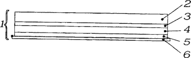
Fig. 1 has shown the sectional view of alms giver's plate 1 optimum structure. Anisotropic crystal film 4 exists Form on the active layer 3, and active layer 3 forms in substrate 2; Crystal film 4 is coated with Varistor layer 5. Structure is coated with protective film 6. Such as needs, protective film can be coated to structure Side or the back side. Plate 9 as follows will removed protective layer 6 rear and anisotropy crystalline substances Varistor layer 5 contacts on the body thin film.
Fig. 2 implements in the method that is subjected to mainboard to form the anisotropic crystal film of arbitrary shape The scheme schematic diagram. Placed on the thermal-conductivity substrate 7 by mainboard 9, and thermal-conductivity substrate 7 is installed in heating On the element 8. Alms giver's plate 1 places and is subjected to mainboard 9 tops, makes crystal film 4 down facing to the acceptor Plate, and substrate 2 is up. For example, consider to have alms giver's plate of structure shown in Figure 1, but do not have the guarantor Sheath. Above the substrate of alms giver's plate, it is roller 10. After applying required driving force, this roller Tube can move to any direction on the surface that is subjected to mainboard. For implementing this method, by first with heating Part 8 adds the thermal acceptor plate and alms giver's plate structure is carried out activation process. After this, by at alms giver's plate base The rolling roller carries out the transfer of anisotropic crystal film desired zone on the surface at the end. Roller Size is determined by the size of anisotropic crystal film transport zone. The heating of every kind of different structure Temperature is determined to set up the condition of appointment of the present invention by experiment with exerting pressure. As mentioned above, real The setting of concrete layer in the structure is depended in the selection of executing concrete scheme of the present invention and theirs is thick Degree and material.
Fig. 3 and 4 is the schematic diagrames for the polarized crystal film configuration of color monitor production. Figure The 3rd, side view, Fig. 4 are upward views. The aeolotropic crystal colour that forms in respective substrates Polarization film (red 11, blue 12, green 13) is wound on the bobbin 14, and is positioned at Be subjected to the below of mainboard 9. Thermal source is arranged below being subjected to mainboard, and this thermal source can be incandescent lamp, or Any other element. Below the substrate of alms giver's plate print head 15 is arranged, its mounting means can On alms giver's plate substrate surface, moving longer distance to required direction under the controlled pressure effect. Seal The size in brush zone is consistent with membrane structure respective element required size. Such as needs, can use many Individual print head, and/or the annex of employing different size. Membrane bobbin and the placement that is subjected to mainboard Make them each other can parallel, thereby can in moving process, form color monitor Polarization film. The activation scheme is selected according to each different concrete condition with pressure.
The description of preferred embodiment
Be the instantiation of embodiment of the present invention below, still, do not include all possible application of open invention.
Embodiment 1
When on substrate of glass, forming alms giver's plate, the moderate glass plate of preparation size at first, its surface through modification with change its with subsequently with intermembranous bonding of the polymer thin that applies.For making glass pane surface hydrophobic, can use dimethyldichlorosilane, hexamethyldisilane, stearic acid and other reagent.The selection of water-repelling agent mainly determines that by the thin polymer film that applies subsequently it should satisfy following requirement: optical clear, hydrophilic, mechanical strength good, level and smooth and be not thicker than 1000
 That satisfies these conditions has, for example, and via topple over celluloid film that celluloid solution (the pentyl acetate solution as 1%) makes or polyvinyl alcohol (as 5% concentration) the PVA film of making by aqueous solution absorption method or centrifugal process to water surface.
Then, prepare two look dyestuffs (dichroic dye) colloidal solution (liquid crystal) and be coated to the surface of thin polymer film, to form anisotropic crystal film with known method.
For making alms giver's plate, [US 5739296 with patent; US 6174394] known method described in detail is coated to liquid crystal film on substrate or the active layer, and this method is based on rod, draw ring and conveying roller processing method.In these methods, the process that applies the liquid crystal solution layer combines with the arrangement of viscous force (viscous force) effect existing supramolecular complex down simultaneously, and above-mentioned viscous force begins to act in coating procedure when liquid level stretching or one deck are mobile with respect to other layers.For the space that is oriented in of setting up polarization axle (polarization axis) on the surface of polarizer changes, the plated film instrument can be subjected to the surface modification moving direction of mainboard.The speed that moves and the change of moving direction will determine the orientation of supramolecular complex in the liquid crystal.
As the organic material of the molecularly oriented that forms liquid crystal, those examples all use known organic material, form the lysotropic liquid crystal phase, and the molecule of this lysotropic liquid crystal phase forms supramolecular complex [US5739296].Liquid crystal is the pre-order state (preordered state) of system, arranges and removes subsequently in the process of desolvating at supramolecular complex, when satisfying required process conditions, forms anisotropic crystal film (crystal film) from above-mentioned pre-order state.
The thickness of layer is by solid concentration in the coating solution and controlled by wet layer thickness.The manufacturing parameter that forms above-mentioned layer has solution concentration, and it is easy to control during the course.The degree of crystallinity of layer can be by X-ray radiography or optical means control.Coating scheme, alignment and dry run combine the crystal structure of guaranteeing film jointly.The optimum condition of degree of crystallinity is for being 3.4 ± 0.2 dusts along crystalline axis direction bragg peak of gained film.Making the crystal film with above-mentioned parameter is subjected on the mainboard subsequently it is coated to.
For the adhesion property that improves anisotropic films and improve its mechanical strength, can apply lacquer thereon.The material of all required auxiliary layers should be transparent in the required SPECTRAL REGION of operation.
Adopt the oxygen plasma method to activate in some cases to improve its adhesion property.
For shift the anisotropic films of required form from the alms giver's plate that makes by said method, adopt flexibility to be subjected to mainboard, this is subjected to mainboard to adopt the optical lens gelatin, is bonded on the alms giver's plate sandwich construction that makes as polyethers, organosilicon, epoxide etc. and print roller.
Then apply the branch split pressure and make whole sandwich construction, thereby anisotropic films is transferred on the flexible carrier from separation on glass.
Utilize above-mentioned methodology and alms giver's plate on glass, can be not alms giver's plate with contacted by mainboard after, and directly in the process of preparation alms giver plate, carry out activation processing.In other words, this operation is included in the process of producing alms giver's plate.The activation carrying out can by to the glass basic surface modification so that it has hydrophobic performance, also can carry out modification, as handling with oxygen plasma to improve its adhesion property to the thin polymer film surface.
Consider the following method example for preparing alms giver's plate, this alms giver's plate will be used to make colored polarisation matrix (colour polarizer matrix) (CPM) subsequently.The making of each color layers of anisotropic films is carried out in two steps.The first step forms continuous anisotropic films on the board surface of smooth planar.This can be flexible polymer film or at first be that glass is subjected to mainboard, and anisotropic films will be subjected to mainboard to transfer on the flexible polymer film (quality that this preparation method is used to improve the anisotropic films of preparation) from this subsequently.
Second step was to transfer to anisotropic crystal film on the layer of the working surface of substrate or alms giver's plate any kind from flexible polymer film, alms giver's plate has preformed burr, and this burr is formed pattern and represents the negative film (negative pattern) of a CPM color through photoetching process by positive photoresist (positive photoresist).Remove photoresist with " blast " photoetching process, remaining is exactly the required pattern that is subjected to ground floor polarization film on the mainboard, and is subjected to mainboard can form the polarization element of multiple other color.
When the CPM of the pure flat lcd screen television set of preparation, glass is at first cleaned in acid Karo by mainboard, and the propanol solution that applies 1% carboxylic acid chromium complex (chromolane) then makes its surface have hydrophobicity.After the drying, the hydrophobic layer that makes, the surface that is subjected to mainboard in 1 hour with 1% polyvinyl alcohol in 110 ℃ of coatings, then in 140 ℃ of dryings 1 hour.And, the anisotropic crystal film coating surface made from the phthalocyanine dye of LLC phase according to method [with reference to US 6174394B1].In order to polyacrylic resin class lacquer coating surface, with rubber coated pressure bowl flexible PET, PETG, donor film are adhesive on the structure made from polyisobutene afterwards then.When the structure that makes subsequently when board separates, polarization film is promptly transferred on the flexible donor film.The flexible PET donor film with dichromatic dye polarization film that this method is made is with 5 seconds of oxygen plasma treatment, and to place relative humidity be 85% humid medium.
The working surface of substrate or structure is used to form and prepares the required alms giver's plate of CPM subsequently, and working surface applies positive photoresist with centrifugal process, dry then, exposure, develops rinsing and dry in argon gas stream in distillation in standard developer.Aforesaid operations forms burr on the surface that is subjected to mainboard, and this burr has been represented the reverted image of the required pattern of film.In oxygen plasma, toasted for 5 seconds by mainboard, and apply 1% the PVA aqueous solution with centrifugal process.Then, be coated with the flexible donor film roll-in of phthalocyanine dye polarization film to being subjected on the mainboard with rubber coated pressure bowl with previously prepared.With 100~150lg/cm
2" interlayer " that compression is made 15 minutes.Then, fusing glue-line and remove the PET donor film in 120 ℃ stove.Afterwards, successively in toluene and another kind of solvent (being main component with toluene, acetone, ethyl acetate usually) cleaning plate (later alms giver's plate) to remove residual glue and lacquer.For making the pattern development of first color layers, working plate (later alms giver's plate) and dioxane were placed ultra sonic bath 2~3 minutes.Be placed in 120 ℃ the stove 30 minutes then with bonding, and then place BaCl with PVC
2In the solution (σ ≈ 30mSm) 20~30 minutes.After being blown into argon gas, polarization matrix is with one deck PVA protection, and this PVA layer is through the centrifugal process coating and 120 ℃ of dryings 30 minutes with 1% the aqueous solution.Apply all operations of photoresist through associating, promptly form the pattern of second color layers to the dry-run protection layer.In addition, select dyestuff benzopurpurin (benzopurpurine) as polarization film.
Scheme in the example can be different.But above-mentioned production operation scheme not only can be used for preparing the process of alms giver's plate, can also be directly used in the process that forms anisotropic crystal film through shifting.
For being formed film, institute (notes, this film can not form in substrate, but be transferred to the substrate of having got ready) at least a portion transfer to polymer from alms giver's plate and be subjected on the mainboard, above-mentioned film is contacted with being subjected to mainboard, wherein to be subjected to mainboard be transparent in the wave-length coverage of operation to polymer, and regional local heat to 45 to be transferred~55 ℃ is activated; The most common ground temperature is in 30~50 or 40~65 ℃ of scopes.The metallic plate that is positioned at below alms giver's plate can provide local heat, and provides the basis for subsequently pressure applies.According to programming rate (gradient), heated sustainable 0.5 minute, can be 0.2~1 minute following heat time heating time in different condition, 1~5 minute, 0.5~10 minute or other.Following condition is satisfied in the selection of activation scheme and used pressure: contrast (contrast) after shifting when constant bit rate (at constant transmission) and/or the change of the double refractive inde of anisotropic crystal film are no more than 10%.The contact is a compression set.And this compression set can be slip dop and matrix print head, and it can apply local action to the selection area that is subjected to mainboard.Scanning is by computer operation.Being printed on the precalculated position carries out.Therefore, be subjected to form on the mainboard optical anisotropic film transparent, its outline drawing looks like to have high-resolution.The anisotropic degree of transport zone is not less than original film.
In matrix method (matrix method), pixel size meets standard point.Can adopt the standard technique of dot matrix printer print head.And, also can adopt stamp (stamp), its shape area can be cut into bulk and fritter.
In an example of disclosed invention embodiment, when transfer has the film of given shape, coated portion image at first only will be subjected to mainboard to rotate to certain angle then and apply another image.The result forms laminated coating, and change has taken place wherein optically anisotropic direction.Above-mentioned technology can be used for forming circulation polarizer etc.
For strengthening transfer process, can use transparent substrates.Then, can adopt the UV light illumination, make the material activation of the middle conversion coating of alms giver's plate (intermediate conversion layer).In addition, this helps to increase anisotropic films and is subjected to bonding between the mainboard and accurately separates its parts.
Also can adopt photochemistry activation (sensibilization).
From a side heating film film is heated up with laser, cause the photochemistry activation (sensibilization) of active layer with the UV lamp from the opposite side illumination.
List of references
[1] Gu Fan etc. (Gvon et al), US 5739296.
[2] gram writing brush etc. (Khan et al), US 6399166.
[3] (Bobrov such as Bo Buluofu, Yu.A.), " the organic dyestuff film thickness of molecularly oriented is to the influence of anisotropic absorption coefficient " (" Dependence of theanisotropic absorption coefficient on the thickness ofmolecularly oriented organic dye films ") (1999). " optical technology magazine " (J.Opt.Technol.) 66 (6), 547-549
[4] RU 2136025 (and EP0961138)
[5] Si Taleier etc. (Staral et al), US 5693446.
[6] in week etc. (Chou et al), US 5506189.
[7] (Fennell such as Fen Naier, L., Lazarev, P., Ohmura, S., Paukshto, M.), " crystal film polarizer-01, the 21 international display research meeting of Asia display/IDW ' and the 8th international display Conference Papers collection " (" Thin CrystalFilm Polarizers
TM"; Asia Display/IDW ' 01; Proceedings of The21st International Display Research Conference inconjunction with The 8th International Display Workshops) Japan; Nagoya; 16-19 day October calendar year 2001,601-603 page or leaf.
[8] (Nazarov such as Na Zhaluofu, V., Ignatov, L., Kienskaya, K.), " electron Spectrum of the aqueous solution and the film that is used for thin film polarizer that makes by liquid crystal ink " (" Electronic spectra of aqueous solutions and films made ofliquid crystal ink for thin film polarizers ") (2001)." molecular material " (Molecular Materials), 14 (2), the 153-163 page or leaf.
[9] gram writing brush etc. (Khan et al), US 6174394B1.
Claims (28)
1. comprise substrate and alms giver's plate of one deck anisotropic crystal film at least, wherein said crystal film is formed by at least a organic material that forms liquid crystal, and its molecule or molecule segment have flat structure; And described crystal film contains the modifier glycerine that helps each zone-transfer at least.
2. according to alms giver's plate of claim 1, wherein the material of anisotropic crystal film contains aromatic ring, and its along the bragg peak of an optical axis direction 3.4 ± 0.2

3. according to alms giver's plate of claim 1, wherein organic material comprises at least a organic dyestuff, and its structural formula contains at least one ion gun group.
4. according to alms giver's plate of claim 3, wherein organic dyestuff comprises the organic dyestuff of at least a following formula: { K} (M) n, K-dyestuff wherein, its chemical formula comprises identical or different ion gun group, the ion gun group is dissolved in the polar solvent to form liquid crystalline phase it, the M-counter ion, the quantity of counter ion in the n-dye molecule, when a counter ion belonged to several molecule, it was a mark, and when n>1, counter ion can be different.
5. according to alms giver's plate of claim 1, wherein crystal film works the function that is selected from following film: polarization film, time-delay film, location film, protective film, or play the film of at least two kinds of above-mentioned film functions simultaneously.
6. according to alms giver's plate of claim 1, wherein anisotropic crystal film is formed by at least two sections, and its optical axis is mutually with 0~90 ° of rotation.
7. according to alms giver's plate of claim 1, wherein adhesion layer is coated on all other layers.
8. according to alms giver's plate of claim 1, wherein light absorber adds base material and/or adhesion layer to, and/or in the anisotropic crystal film.
9. according to alms giver's plate of claim 1, wherein light absorber adds in the material that forms adhesion layer.
10. according to alms giver's plate of claim 1, wherein substrate is made by polymeric material or glass or semi-conducting material or metal.
11. according to alms giver's plate of claim 1, wherein substrate has smooth or projection or recessed surface configuration.
12. according to alms giver's plate of claim 1, the amount that wherein said modifier glycerine adds in the crystal film material is less than 0.1 weight %.
13. according to alms giver's plate of claim 1, wherein anisotropic crystal film applies with at least one the regional form that shifts required image subsequently.
14. alms giver's plate according to claim 2, wherein substrate surface is through modification and become hydrophobic, apply optically transparent material subgrade above the substrate at this with water-wetted surface, and anisotropic crystal film is coated on the described subgrade with at least one the regional form that shifts required image subsequently, and one deck adhesion layer is at least arranged above it.
15. according to alms giver's plate of claim 1, wherein at least a portion of anisotropic crystal film applies with the different area format of color.
16. according to alms giver's plate of claim 1, wherein anisotropic crystal film is handled with divalence or trivalent metal ion and is made it change water-fast phase into.
17., be used for by shifting anisotropic films to be subjected to mainboard to form anisotropic crystal film from alms giver's plate according to alms giver's plate of claim 1.
18. one kind is shifted by alms giver's plate of claim 1 and in the method that is subjected to form on the mainboard anisotropic crystal film, comprising:
Make and contacted with the alms giver's plate that comprises at least one anisotropic crystal film of claim 1 by mainboard;
Activation comprises at least a portion of whole alms giver's plate of anisotropic crystal film to be transferred, and/or be subjected at least a portion of mainboard, wherein activation degree is should be enough high so that film can shift down exerting pressure subsequently, but be not high to foot in the crystal structure that destroys the crystal film that shifts; And
In activation, or after activation, at least comprising being transferred in whole alms giver's plate exerted pressure by the part of the crystal film on the mainboard, wherein stress level should be high enough at least a portion that makes film and transfers to from alms giver's plate and be subjected to mainboard, but be not high to foot in the crystal structure that destroys the crystal film that shifts.
19. according to the method for claim 18, following condition is satisfied in the selection that wherein activates scheme and used pressure: shift contrast and/or the double refractive inde change of back anisotropic crystal film when the constant rate of transform and be no more than 10%.
20. according to the method for claim 18, wherein anisotropic crystal film is to be made by the liquid crystal of at least a organic material, described organic material externally forms the lysotropic liquid crystal phase through being coated under the alignment in the substrate.
21. according to the method for claim 18, wherein alms giver's plate is alms giver's plate of one of claim 1-17.
22. according to the method for claim 18, wherein activation makes the intensity of at least one layer material of alms giver's plate reduce and/or make the bonding decline of alms giver's plate at least two interlayers, and/or makes the upper strata and be subjected to bonding increase between the mainboard.
23. want 18 method according to right, wherein activation is through applying heat, electromagnetism or other effect and carry out the alms giver being firm and hard.
24. according to the method for claim 18, wherein activation and pressure are applied at least a portion of the whole alms giver's plate that comprises crystal film to be transferred.
25., wherein activates on the part of the whole alms giver's plate that comprises crystal film to be transferred and carry out, and pressure is applied to the whole surface of alms giver's plate to be transferred according to the method for claim 18.
26., wherein activates on whole alms giver's plate and carry out, and pressure is applied to the part that whole alms giver's plate comprises crystal film to be transferred according to the method for claim 18.
27. according to the method for claim 18, wherein activate in preparation alms giver plate process, with before alms giver's plate contacts do not carry out as yet in substrate.
28. according to the method for claim 27, the shape of anisotropic crystal film wherein to be transferred forms before preparation alms giver plate or with before contacted by mainboard does not form on alms giver's plate of getting ready at it.
Applications Claiming Priority (2)
| Application Number | Priority Date | Filing Date | Title |
|---|---|---|---|
| RU2002102943/28A RU2002102943A (en) | 2002-02-06 | A method of forming an anisotropic crystalline film on a substrate by transferring from a carrier plate, a carrier plate of an anisotropic crystalline film and a method for its manufacture | |
| RU102943/2002 | 2002-02-06 |
Publications (2)
| Publication Number | Publication Date |
|---|---|
| CN1688396A CN1688396A (en) | 2005-10-26 |
| CN100411753C true CN100411753C (en) | 2008-08-20 |
Family
ID=27656549
Family Applications (1)
| Application Number | Title | Priority Date | Filing Date |
|---|---|---|---|
| CNB038055104A Expired - Fee Related CN100411753C (en) | 2002-02-06 | 2003-02-06 | Method of fabricating anisotropic crystal film on a receptor plate via transfer from the donor plate, the donor plate and the method of its fabrication |
Country Status (7)
| Country | Link |
|---|---|
| US (1) | US6841320B2 (en) |
| EP (1) | EP1481281B1 (en) |
| JP (1) | JP4133833B2 (en) |
| KR (1) | KR100632082B1 (en) |
| CN (1) | CN100411753C (en) |
| AU (1) | AU2003216178A1 (en) |
| WO (1) | WO2003067312A2 (en) |
Families Citing this family (16)
| Publication number | Priority date | Publication date | Assignee | Title |
|---|---|---|---|---|
| US6841320B2 (en) * | 2002-02-06 | 2005-01-11 | Optiva, Inc. | Method of fabricating anisotropic crystal film on a receptor plate via transfer from the donor plate, the donor plate and the method of its fabrication |
| US7297209B2 (en) | 2003-12-18 | 2007-11-20 | Nitto Denko Corporation | Method and device for transferring anisotropic crystal film from donor to receptor, and the donor |
| US20080049321A1 (en) * | 2006-08-25 | 2008-02-28 | Jds Uniphase Corporation | Passive Depolarizer |
| US8767133B2 (en) | 2009-02-17 | 2014-07-01 | 3M Innovative Properties Company | Optical control devices and methods of making |
| KR101040144B1 (en) * | 2009-04-02 | 2011-06-09 | 주식회사 효성 | A method of producing a phase difference film and a phase difference film film produced by the method |
| KR101706232B1 (en) * | 2010-06-29 | 2017-02-15 | 엘지디스플레이 주식회사 | Touch Panel |
| US9360596B2 (en) | 2013-04-24 | 2016-06-07 | Light Polymers Holding | Depositing polymer solutions to form optical devices |
| US9829617B2 (en) | 2014-11-10 | 2017-11-28 | Light Polymers Holding | Polymer-small molecule film or coating having reverse or flat dispersion of retardation |
| US9856172B2 (en) | 2015-08-25 | 2018-01-02 | Light Polymers Holding | Concrete formulation and methods of making |
| CN106410422A (en) * | 2016-10-28 | 2017-02-15 | 东南大学 | 3-bit transmission type electromagnetic code metamaterial applied in terahertz band |
| US10403435B2 (en) | 2017-12-15 | 2019-09-03 | Capacitor Sciences Incorporated | Edder compound and capacitor thereof |
| US10962696B2 (en) | 2018-01-31 | 2021-03-30 | Light Polymers Holding | Coatable grey polarizer |
| KR101936356B1 (en) * | 2018-01-31 | 2019-01-08 | 주식회사 레다즈 | Apparatus and method for transferring micro element to target object |
| US11370914B2 (en) | 2018-07-24 | 2022-06-28 | Light Polymers Holding | Methods of forming polymeric polarizers from lyotropic liquid crystals and polymeric polarizers formed thereby |
| KR102262913B1 (en) * | 2019-12-31 | 2021-06-09 | 광운대학교 산학협력단 | Metasurfaces for realizing polarization rotation and focusing |
| CN113218772B (en) * | 2021-03-25 | 2022-05-03 | 厦门大学 | Film mechanical strength characterization method and device based on film passing pressure test |
Citations (5)
| Publication number | Priority date | Publication date | Assignee | Title |
|---|---|---|---|---|
| US4923860A (en) * | 1988-10-18 | 1990-05-08 | Eastman Kodak Company | Method of making a color filter array using light flash |
| US4978652A (en) * | 1988-10-18 | 1990-12-18 | Eastman Kodak Company | Method of making a color filter array element using a heated embossed surface |
| US5024989A (en) * | 1990-04-25 | 1991-06-18 | Polaroid Corporation | Process and materials for thermal imaging |
| US5693446A (en) * | 1996-04-17 | 1997-12-02 | Minnesota Mining And Manufacturing Company | Polarizing mass transfer donor element and method of transferring a polarizing mass transfer layer |
| US5739296A (en) * | 1993-05-21 | 1998-04-14 | Russian Technology Group | Method and materials for thermostable and lightfast dichroic light polarizers |
Family Cites Families (19)
| Publication number | Priority date | Publication date | Assignee | Title |
|---|---|---|---|---|
| JPS62146960A (en) | 1985-12-19 | 1987-06-30 | Teijiro Kitao | Naphthoquinone charge transfer complex |
| US4743463A (en) | 1986-02-21 | 1988-05-10 | Eastman Kodak Company | Method for forming patterns on a substrate or support |
| IL88099A (en) | 1987-11-06 | 1992-02-16 | Chinoin Gyogyszer Es Vegyeszet | Lyotropic liquid crystalline compositions |
| US5156938A (en) | 1989-03-30 | 1992-10-20 | Graphics Technology International, Inc. | Ablation-transfer imaging/recording |
| DE4209873A1 (en) * | 1991-03-26 | 1992-10-01 | Fuji Photo Film Co Ltd | Positive and negative photocopy prodn. - by exposure to change adhesion between light heat transformation coat and copying coat and image transfer |
| US5308737A (en) | 1993-03-18 | 1994-05-03 | Minnesota Mining And Manufacturing Company | Laser propulsion transfer using black metal coated substrates |
| US5691103A (en) * | 1995-02-17 | 1997-11-25 | Konica Corporation | Image forming material, method of preparing the same and image forming method employing the same |
| US5693447A (en) * | 1995-02-17 | 1997-12-02 | Konica Corporation | Image forming material, method of preparing the same and image forming method employing the same |
| US6399166B1 (en) * | 1996-04-15 | 2002-06-04 | Optiva, Inc. | Liquid crystal display and method |
| JPH10221526A (en) * | 1997-02-12 | 1998-08-21 | Toshiba Corp | Phase diffraction grating and liquid crystal disiply element using it |
| US6114088A (en) * | 1999-01-15 | 2000-09-05 | 3M Innovative Properties Company | Thermal transfer element for forming multilayer devices |
| JP2001004822A (en) * | 1999-06-23 | 2001-01-12 | Fuji Photo Film Co Ltd | Manufacture of color filter |
| RU2178900C2 (en) | 2000-02-25 | 2002-01-27 | ОПТИВА, Инк. | Dichroic polarizer and material for its manufacture |
| US6630289B1 (en) * | 2000-08-22 | 2003-10-07 | The Hong Kong University Of Science And Technology | Photo-patterned light polarizing films |
| RU2225025C2 (en) | 2000-12-06 | 2004-02-27 | ОПТИВА, Инк. | Liquid-crystal device for information display |
| CN1460282A (en) | 2001-02-07 | 2003-12-03 | 奥普逖娃公司 | Method of obtaining anisotropic crystalline films and device for implementation of method |
| US6485884B2 (en) * | 2001-04-27 | 2002-11-26 | 3M Innovative Properties Company | Method for patterning oriented materials for organic electronic displays and devices |
| JP2002343564A (en) * | 2001-05-18 | 2002-11-29 | Sharp Corp | Transfer film and manufacturing method of organic electroluminescence element using the same |
| US6841320B2 (en) | 2002-02-06 | 2005-01-11 | Optiva, Inc. | Method of fabricating anisotropic crystal film on a receptor plate via transfer from the donor plate, the donor plate and the method of its fabrication |
-
2003
- 2003-02-04 US US10/358,607 patent/US6841320B2/en not_active Expired - Lifetime
- 2003-02-06 JP JP2003566605A patent/JP4133833B2/en not_active Expired - Lifetime
- 2003-02-06 WO PCT/US2003/003521 patent/WO2003067312A2/en active Application Filing
- 2003-02-06 EP EP03737659.7A patent/EP1481281B1/en not_active Expired - Lifetime
- 2003-02-06 CN CNB038055104A patent/CN100411753C/en not_active Expired - Fee Related
- 2003-02-06 KR KR1020047012199A patent/KR100632082B1/en active IP Right Grant
- 2003-02-06 AU AU2003216178A patent/AU2003216178A1/en not_active Abandoned
Patent Citations (5)
| Publication number | Priority date | Publication date | Assignee | Title |
|---|---|---|---|---|
| US4923860A (en) * | 1988-10-18 | 1990-05-08 | Eastman Kodak Company | Method of making a color filter array using light flash |
| US4978652A (en) * | 1988-10-18 | 1990-12-18 | Eastman Kodak Company | Method of making a color filter array element using a heated embossed surface |
| US5024989A (en) * | 1990-04-25 | 1991-06-18 | Polaroid Corporation | Process and materials for thermal imaging |
| US5739296A (en) * | 1993-05-21 | 1998-04-14 | Russian Technology Group | Method and materials for thermostable and lightfast dichroic light polarizers |
| US5693446A (en) * | 1996-04-17 | 1997-12-02 | Minnesota Mining And Manufacturing Company | Polarizing mass transfer donor element and method of transferring a polarizing mass transfer layer |
Also Published As
| Publication number | Publication date |
|---|---|
| EP1481281A4 (en) | 2011-01-12 |
| EP1481281B1 (en) | 2013-07-31 |
| CN1688396A (en) | 2005-10-26 |
| AU2003216178A1 (en) | 2003-09-02 |
| US6841320B2 (en) | 2005-01-11 |
| EP1481281A2 (en) | 2004-12-01 |
| US20030148196A1 (en) | 2003-08-07 |
| WO2003067312A2 (en) | 2003-08-14 |
| JP4133833B2 (en) | 2008-08-13 |
| KR100632082B1 (en) | 2006-10-04 |
| JP2005517207A (en) | 2005-06-09 |
| WO2003067312A3 (en) | 2004-01-08 |
| AU2003216178A8 (en) | 2003-09-02 |
| KR20040104955A (en) | 2004-12-13 |
Similar Documents
| Publication | Publication Date | Title |
|---|---|---|
| CN100411753C (en) | Method of fabricating anisotropic crystal film on a receptor plate via transfer from the donor plate, the donor plate and the method of its fabrication | |
| JP6662299B2 (en) | Optical filter and device using the same | |
| CN100380145C (en) | Light polarizing film | |
| CN100529880C (en) | Method for preparing photo-patterned light polarizing films | |
| WO2015099060A1 (en) | Optical filter | |
| AU2011280094B2 (en) | Multi-layer articles capable of forming color images and methods of forming color images | |
| JP5227596B2 (en) | Method for producing article having birefringence pattern | |
| JP2014197231A (en) | Clear to circular polarizing photochromic device and method of making the same | |
| JP2009193014A (en) | Patterning elliptical polarizer | |
| JP2009223190A (en) | Process of producing patterned birefringent product | |
| JP2019512742A (en) | Method of manufacturing flexible display device | |
| CN103809232A (en) | Method for manufacturing phase difference plate and phase difference plate manufactured by same | |
| CN108292000A (en) | Optical film | |
| JP2001004823A (en) | Color filter | |
| WO2021059849A1 (en) | Dispersion, composition, cured film, color filter, solid-state imaging element, and image display device | |
| KR20210035234A (en) | Curable composition, cured film, pattern formation method, optical filter and optical sensor | |
| KR102521207B1 (en) | Manufacturing method of mobile phone decoration film and mobile phone decoration film manufactured through the same | |
| JP6505833B2 (en) | Polarizing element in which a film having high retardation and a layer containing a dichroic dye are laminated, and a display device provided with the same | |
| CN114761841A (en) | Optical laminate and image display device | |
| TW201241489A (en) | Optical filter and liquid crystal display including the same | |
| JP2007072268A (en) | Optical part and its manufacturing method | |
| JP4076238B2 (en) | Color filter for fluorescent display tube | |
| KR20200000374A (en) | Method for manufacturing polarizing plate | |
| JP2022076599A (en) | Film | |
| JPH05139042A (en) | Image recording laminated film |
Legal Events
| Date | Code | Title | Description |
|---|---|---|---|
| C06 | Publication | ||
| PB01 | Publication | ||
| C10 | Entry into substantive examination | ||
| SE01 | Entry into force of request for substantive examination | ||
| C14 | Grant of patent or utility model | ||
| GR01 | Patent grant | ||
| CF01 | Termination of patent right due to non-payment of annual fee |
Granted publication date: 20080820 Termination date: 20170206 |
|
| CF01 | Termination of patent right due to non-payment of annual fee |