Detailed Description Of The Invention
In simple terms, the network processing unit by the IP voice-over can be used for transmitting computer and voice data simultaneously at the computer network of packetizing.The integrated circuit that comprises connection processing device and different peripheral according to the network processing unit of one embodiment of the invention.Especially, this network processing unit comprises an integrated USB (USB), IEEE 802.3 medium access controllers (MAC), a transponder and a pair of integrated PCM HDLC port, this port can dock peripheral hardwares such as A/D (analog/digital) transducer and D/A (digital-to-analog) transducer at an easy rate with processor.These Peripheral Interfaces are that (FlexiblePeripheral Interconnect, FPI) bus is integrated in the middle of the processor by a flexible peripheral interconnection.
Network processing unit according to another embodiment of the invention comprises a flush bonding processor, a packet handler, a speech processor and a cell/frame processor, and all these parts all are coupled on the system bus.The parts that are coupled on the bus comprise that also one is used for handling interrupt and the peripheral control processor of direct memory access (DMA) (DMA) function, a buffer storage and a plurality of peripheral hardware.Packet interface can dock with multiple Packet Based Network, for example, and by the local area network (LAN) of 10/110bT interface butt joint, WLAN (wireless local area network), universal serial bus networks, perhaps home telephone network joint network.The cell/frame processor can provide and be used for and atm network, frame-relay network or based on the network butt joint of xDSL.
The block diagram of Fig. 1 for making up according to enforcement of the present invention, pass through the telephone system of Internet protocol (IP) voice-over.Telephone system 10 comprises a network processing unit 12, and it carries out various functions, comprises that the voice signal with numeral is assembled into a succession of grouping and transmits and receive grouping by local area network (LAN) 13.
Local area network (LAN) can be coupled to the wide area network as the Internet by a gateway (not showing in the drawings).Telephone system 10 also comprises a microphone 14a, loud speaker 14b and mobile phone 14c, and these all are connected on the network processing unit 12 by a digital-to-analog/analog to digital (DA/AD) transducer 22.DA/AD transducer 22 is to be connected on the network processing unit 12 by an integrated pulse code modulation (pcm) port 24, and this is further described below.Each PCM port can be handled nearly 30 time slots and each time slot can be handled 64K bps voice channel.Therefore this PCM port is just as the internal hardware of IP processor and the interface between the external equipment.Except transmitting and receiving the voice data, this telephone system also transmits and receives the data from workstation1 8, and this work station is connected on the network processing unit 12 by an ethernet port 26.Another ethernet port 28 is used to connect network processing unit and local area network (LAN) 13.
The user can dial phone number with the keyboard 30 that is docked to network processing unit 12, and provides a LCD display 32 so that the user can see the information of importing on keyboard.At last, telephone system 10 comprises a memory cell 34 and is used for storage networking processor 12 needed programs and other data.
Fig. 2 is the block diagram of network processing unit 12, and its details is described in detail in the design instruction of " Harrier-VT " at annex A title.Network processing unit 12 comprises core processor 202, internal bus 34, bus control unit 204, data storage cell 206, program storage unit (PSU) 208, code storage unit 209, external bus interface unit 210, outside master unit 212, peripheral control processor 214, the Power Management Unit 216 that comprises monitoring clock 215, system timer 222, general timer unit 220, serial line interface 226, parallel port module 227, the clock of forming by crystal oscillator 250 and phase-locked loop 218, JTAG/OOCS port 228, FPI bridge 252, and be used for ethernet port 40, USB port 56, interface with PCM port 24.
Core processor 202 demonstration ground are InfineonTechnologies, the TriCore processor that Corp. produces.TriCore is the microcontroller/DSP kernel of one 32 bit, it comprises two supports integer and packs into/and the main flow waterline of storage operation and the streamline of the 3rd support optimization DSP cycling.
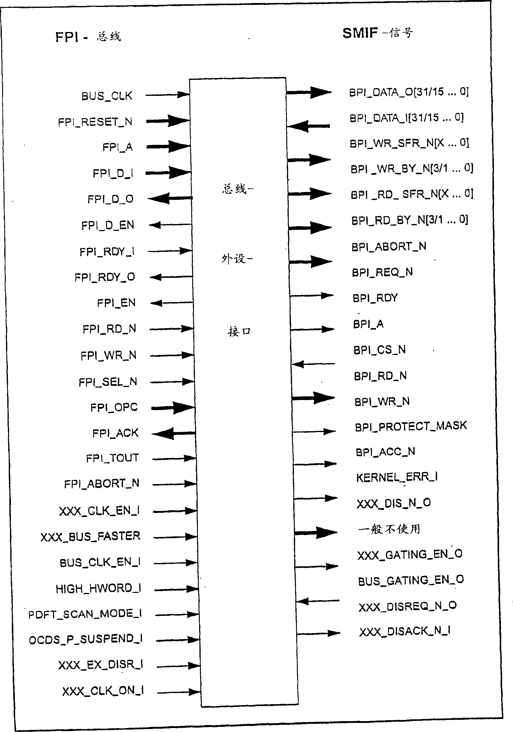
What internal bus 34 was demonstrated is a FPI bus, and annex C is asked for an interview in detailed description respectively and D, title are the design instruction of " peripheral interconnection bus is 3.2 editions flexibly " and " BPI technical specification draft 0.9 edition ".In simple terms, FPI bus 34 is a high speed, 32 bit addresses/data/address bus, supports the burst read-write of 2,4 or 8 words.
Bus arbitration between the FPI bus master controller of bus control unit 204 process chip levels (promptly being used to support jtag port 228, peripheral control processor 214, outside master unit 212, program storage unit (PSU) 208, data storage cell 206, the transmission Data Management Unit 24A that debugs and receive Data Management Unit 24B).When need one of addressing invalid/during non-existent unit it also as default bus from the unit, and catch bus error and overtime incident.
Data storage cell 206 is used for storing data, and it comprises the local storage of a chip-scale, a speed buffering is deposited memory and the interface to internal bus 34.
Program storage unit (PSU) 208 is to be used for stored programly, and it comprises the local storage of a chip-scale, cache memory and the interface to internal bus 34.
Code storage unit 206 is side program memories, and it is directly connected on the program storage unit (PSU) 208.
External bus unit 210 provides the interface between processor 12 and the system equipment.In the embodiment illustrated, external bus unit 210 comprises 24 bit addresses and 32 bit data bus of a demultiplexing, and for example can be docked to external ROM, EPROM, SRAM and synchronous dram.
Outside master unit 212 is that a chip is selected pin, uses an external bus master unit to come a address on the access internal bus 34.
Peripheral control processor 214 is as dma controller and break in service processor.It has unloaded the burden of most of interruptions that are pressed for time for CPU.Briefly, peripheral control processor 214 is microcontrollers that are used for programmable, the drives interrupts of transfer of data and peripheral hardware control, and it has also comprised the instruction that is used for DMA and bit process simultaneously.
Processor 12 comprises 3 timing units: monitoring clock 215, system timer 222 and general timer unit 220.Monitoring clock 215 provides a kind of mechanism of recovering from hardware or software failure.System timer 222 is the 56 bit timers that high accuracy is long-term, and it provides the system time of an overall situation for operating system and other purposes.General timer unit 220 comprises three general 32 bit timer 220a, 220b, 220c.These three timers can be used in timed events, counting event and the recording events.In addition, these timers both can move under stand-alone mode, also can link together to solve more complicated task.
Three serial line interface 226: one synchronous serial channels 226a and two asynchronous serial communication interface 226b and 226c also are provided.Synchronous serial channel 226a supports the full and half duplex synchronous communication between processor 12 and other external equipments such as microcontroller and microprocessor.Asynchronous 226b of connecing and 226c both can asynchronously also can operate synchronously.
Parallel port module 227 is ports of one 8 bit width, and it provides general I/O (I/O) function.
Phase-locked loop 218 comprises a clock synthesizer/oscillating circuit 218A.PLL218 allows to be connected to the crystal oscillator 250 of chip-scale, perhaps is connected on external crystal or the clock.
Power Management Unit 216 allows to regulate passes through battery-operated equipment.Power Management Unit 216 comprises a reset system 217, and it is mainly used in and powers up, the replacement of hardware, software and monitoring clock.
USB port 56 and network processing unit 12 are integrated on the same circuit, describe in detail to ask for an interview the design instruction that the accessories B acceptance of the bid is entitled as " universal serial bus device controller 1.1 editions ".
For network processing unit 12 is directly connected on the local area network (LAN), processor has comprised an IEEE 802.3 and has connect 40, according to ieee standard, comprises a pair of IEEE 802.3 medium access controller 70a and 70b and a transponder 70c in this interface.
In USB port, 802.3 MAC and the PCM port each all is connected on the internal bus, is respectively the flexible peripheral interconnection bus 34 described in the design instruction of " flexibly peripheral interconnection bus 3.2 editions " and " BPI technical specification draft 0.9 edition " as title in annex C and D.
As mentioned above, for provide one easily interface connect DA/AD transducer 22, network processing unit 12 has comprised a pair of integrated PCM port 24.The PCM port comprises some subassemblies, comprises Data Management Unit delivery module 24A and data management receiver module 24B etc., and details is asked for an interview annex E and F is entitled as the design instruction of " grand technical specification DMUT2.2 version " and " grand technical specification DMUR2.2 version " respectively.
In addition, the PCM port also comprises transmission buffer 24C and reception buffer 24D, and details is asked for an interview among annex G, H and the I design instruction that is entitled as " grand technical specification TB2.1 version ", " grand technical specification TB tables of data " and " reception buffer 2.1 editions " respectively.
PCM port 24 also comprises a protocol machine and transmits 24E and receiver module 24F, describes in detail to ask for an interview among annex J and the K design instruction that is entitled as " protocol machine transmits 2.2 editions " and " grand technical specification PMR2.1 version " respectively.
The time slot surrenderee receives 24G and delivery module 24H is also contained in the PCM port 24, and the design instruction that is entitled as " the time slot allocation device receives the 2.2.1 version " and " the time slot allocation device transmits the 2.2.1 version " is respectively asked for an interview among annex L and the M in detailed explanation.
PCM port 24 also comprises a reception/delivery port module 24I/24J, and details is asked for an interview among the annex N design instruction that is entitled as " reception/delivery port interface 2.3.1 version ".
Data management transmission and receiver module 24A and 24B are connected to FPI bus 34 by the interface 24L and the 24M of a master/slave formula, and details is asked for an interview in the annex 0 design instruction that is entitled as " platform notion: SMIF technical specification 1.0 editions ".
The remaining part of PCM port 24 is connected to FPI bus 34 by a BPI interface 24K, describes in detail to ask for an interview among the annex D design instruction that is entitled as " BPI technical specification draft 0.9 edition ".
Fig. 3 is the block diagram according to the integrated access device of an alternative embodiment of the invention, the multiple parts of this equipment at annex A and/or annex P, be entitled as in the file of " PEB 4,261 0.1 editions " more detailed description arranged.This integrated access device controller comprises a flush bonding processor 302 that all is coupled on the system bus 334, the TriCore that produces of Infineon Tchnologies Corp. for example, 306, one speech processors 308 of a packet handler, and a cell/frame processor 310.System bus 334 demonstration be a FPI bus, describe in detail and ask for an interview annex C and D is entitled as the design instruction of " peripheral interconnection bus is 3.2 editions flexibly " and " BPI technical specification draft 0.9 edition " respectively.
Be coupled to equally on the FPI bus 334 is a peripheral control processor that is used for handling interrupt and direct memory access (DMA) (DMA) function 304, a buffer storage 312 and an a plurality of peripheral hardware 316.PCP processor 304 and peripheral hardware 316 can be the known devices that is relevant to the TriCore flush bonding processor.
TriCore is the microcontroller/DSP kernel of one 32 bit, and it comprises two supports integers and pack into/and the main flow waterline of storage operation and the 3rd support the streamline of the DSP cycling optimized.
Packet handler 306 comprises a FPI bridge 380 to be docked to FPI bus 334, PCP grouping preprocessor 350 and multiple I/O unit, comprises ethernet port 352, wireless lan port 354, USB (universal serial bus) port 356 and family expenses PNA (telephone wire networking associating) port 358.The I/O unit of packet handler is coupled to a work station (not drawing among the figure), for example personal computer.The visible accessories B of the description of the USB port of a demonstration, maybe can be illustrated in submitted on April 7th, 2000, sequence number is 09/545,393, be entitled as the U.S. Patent application of " USB Interfacing UsingFIFO Buffers (using the USB butt joint of fifo buffer) ".Ethernet port 352 is realized according to IEEE 802.3 standards.Wireless lan port 354 can be realized as IEEE 802.11WLAN standard.HPNA port 358 can be realized family expenses PNA 2.0; Similarly port can obtain from manufacturers such as NetGear and D-Link.
Speech processor 308 is coupled on the public switched telephone network, and comprises a FPI bridge 382, PCM port that at least one is integrated 360, a mailbox 362 and a DSP 364.
PCM port 360 is described with reference to annex E-O above generally being similar to, and the title of this annex is respectively " grand technical specification DMUT2.2 version ", " grand technical specification DMUR2.2 version ", " grand technical specification TB2.1 version ", grand technical specification TB tables of data ", " reception buffer 2.1 editions ", " protocol machine transmits 2.2 editions ", " grand technical specification PMR2.1 version ", " the time slot allocation device receives the 2.2.1 version ", " the time slot allocation device transmits the 2.2.1 version ", " reception/delivery port interface 2.3.1 version ", " platform notion: SMIF technical specification 1.0 editions ".
Digital signal processor (DSP) 364 and mailbox 362 can resemble present existing system, as the DSP of similar TriCore embedded controller, equally realize.
Cell/frame processor 310 is to be used for sending and receive cell and/or frame by the packet network of various criterion.Therefore, cell/frame processor 310 can comprise frame processor 368 and ATM cell processor 370.It is frame relay port 314b, Utopia interface 314a and the PCM port 314c that is used to dock the XDSL channel that multiple different input/output end port: SCC (V.35) can also be provided in the cell/frame processor.Also can provide other packet network interfaces, as Ethernet interface etc.
In addition, cell/frame processor 310 can realize encrypting the communication of protecting along packet network.Specifically, ciphering unit 366 can be realized the function described among the annex Q.
Network processing unit 312a realizes the grouping and the frame pattern of operating usually.In group mode, system 312a can be coupled to local area network (LAN) by 10/100bT interface 352, be coupled to WLAN (wireless local area network) by WLAN interface 354, be coupled to network, perhaps be coupled to network based on home telephone by HPNA interface 358 based on USB by USB interface 356.350 monitoring of grouping processor controls transmit by the data that these interfaces carry out.
For example, at work, voice are by outside voice encryption device (not drawing among a figure) coding that is connected to one of PCM port 360.Voice data behind the coding is sent to external memory storage (for example by DRAM interface 335) by bus 334.Processor 302 sense data from memory is carried out voice compression, then it is write back in the external memory storage.Next step, one of packet interface 352,354,356,358 is read and be forwarded to speech packet by bus 334 again in external memory storage.Data are then by the suitable network of feed-in.
In receive direction, suitable interface 352,354,356,358 monitoring services.In case detect, corresponding packet just is sent in the external memory storage.Processor 302 reads in this data, carries out voice compression, and it is write back to external memory storage.Data are delivered to outer decoder (not drawing among the figure) by pcm interface then.
In the cell/frame pattern, system can be coupled to the ATM25 network by interface 314a, and 314b is coupled to frame-relay network by interface, or is coupled to the xDSL network by interface 314c.At work, voice are encoded by the outside voice encryption device that is connected to one of PCM port 360 (not drawing among the figure).Voice data behind the coding is sent to external memory storage (for example by DRAM interface 335) by bus 334.Processor 302 reads in data from memory, carry out voice compression, and then it is write back to external memory storage.Next step, voice data is read and is forwarded to cell/frame processor 310 once more from external memory storage by bus 334.Cell/frame processor 310 can be encrypted with ciphering unit 366.Then, be which network according to what be coupled to processor, data format in frame processor 368 or ATM/ cell processor 370.Final data is fed to suitable network.
In receive direction, suitable interface 314a, 314b, 314c monitoring service.In case detect, this frame or cell are just gone format and are delivered to external memory storage.Processor 302 reads in this data, carries out voice compression, and it is write back in the external memory storage.Then, data send outer decoder (not drawing among the figure) to by pcm interface 360.
As mentioned above, the present invention is a network processing unit by the IP voice-over, and it comprises integrated interface port, makes this processor can be coupled to various external components and peripheral hardware at an easy rate.
Annex A
Exercise question:
HARRIE?-VT
3 general views
HARRIER-VT provides a kind of being used for to carry the integrated single-chip solution of height that fax (FoIP) is used by IP voice-over (VoIP) with by IP.This solution has been modified to serve such as application such as VoIP cable modem, residential gateway, lan telephone drawn game field adapters.
HARRIER-VT based on be 32 up-to-date bit TriCore structures of Infineon.These high-end 32 bit list kernel CISC/RISC/DSP with two MAC and SIMD ability provide a kind of MIPS budget, it be suitable on an equipment, moving simultaneously such as G.7xx high compression/low time delay audio codec and such as H.323, the VoIP protocol stack of x.GCP or SIP etc.
The real time operating system support that comprises VxWorks, Nucleus+ and PSOS etc. provides the visit to the commercial and proprietary application software product of wide range.
This structure based on be flexible peripheral interface bus (FPI), 32 bit TriCore that it will embed and multiple private communication module interconnects.Except synchronously and the Asynchronous Serial Interface (USART, IrDA, SPI) of standard, HARRIER-VT also provides similar 10/100Base-TMII Ethernet, general purpose I/O, towards the PCM port of time slot and the interface of USB (USB).
HARRIER-VT has the software module that a cover provides API simultaneously, and it can allow the user develop complete system scheme effectively.These softwares can be applicable to several operation systems at an easy rate.Protocol software API allows simple integrated third-party upper-layer protocol software (for example H.323, H.450.x or x.GCP) and user's application software.Such as G.711, G.723.1 (comprise VAD and CNG), G.726, G.729A, G.729E, echo eliminate (AEC) but and voice compression algorithm such as DTMF can provide with the form of hyperlink target code.
Assessment tool EASY4261 will can get with the engineering sample of HARRIER-VT simultaneously.It can be used for carrying out all functions of HARRIER-VT and the IP operation of generation and analysis user definition, or is that test and purpose of appraisals are caught the traffic carrying capacity that enters.VoIP will be equipped with based on H.323 complete VoIP with reference to instrument and be used, and insert card or independent development board as PCI.
For software development and debugging, the complete instrument chain (comprising C/C++ compiler, linker, locator, profile, assembler and debugger) of a cover will be provided by our instrument partner such as Tasking, Greenhills and GNU.
| Type |
Encapsulation |
| PEB?XXXX |
?F-TQFP-2 |
3.1 characteristics
3.1.1?TriCore(CPU)
TriCore is a kind of 32 bit CISC/RISC/DSP with two MAC and SIMD ability, and optimizes for real time embedded system.It is embodied as and has the absolute address that is used for program and data storage and the Harvard structure of data/address bus.It has three streamlines: arithmetic, pack into/store and loop control.
The single kernel of high-performance 80MHz CISC/RISC/DSP
32 bits are packed into/storage organization
Two instructions are sent
4G byte address scope (2
32)
General purpose register set:
-16 32 Bit data registers
-16 32 bit addresses registers
The shadow register that is used for the fast context exchange
Automatically context enters to preserve and withdraw from and recovers to be used for:
-subprogram
-interrupt
-trap
Two groups of memory protection registers
Data type:
-boolean
-saturated integer
-bit array
-the symbol mark arranged
-character
-double word integer
-the symbol integer arranged
-unsigned int
-IEEE-754 single-precision floating point type
Data format
-bit
-byte (8 bit)
-half-word (16 bit)
-word (32 bit)
-double word (64 bit)
Instruction type
-arithmetic
-relatively
-logic
-displacement
-bit logic
-bit field
The data of-compression
The addressing of-arithmetic
-relatively addressing
-MAC
-coprocessor
-branch
-pack into/store
-system
Command format:
-16 bits
-32 bits
Addressing system:
-absolute
-circulation
-antiposition
-base address+side-play amount
-have base address+side-play amount that pre-renewal and back are upgraded
The multiplication and the instruction (MAC) that adds up
-two 16 * 16
-16×32
-32×32
Zero-overhead loop
Area=5mm
2
Power=1.5 milliwatts/MHz is at 2.25 volts
3.1.2 internal bus (FPI)
The FPI bus is the high-speed internal bus that makes the peripheral interconnection of TriCore kernel and inside.Details is asked for an interview " peripheral interconnection bus 3.3 editions ".Realize that specific characteristics are as follows:
2,4 or 8 word burst read-writes
Do not have to cut apart to transmit and support
32 bit addresses and data/address bus
1 master unit, 6 master/slave unit are connected from the unit with 15
The streamline support of limited single master unit
3.1.3 bus control unit (BCU)
Bus arbitration in the process chip between each FPI bus master unit:
-be used to debug the JTAG/OCDS port (TCU) of support
-peripheral control processor (PCP)
-outside master unit (XMU)
-TriCore program storage unit (PSU) (PMU)
-TriCore data storage cell (DMU)
-transmission Data Management Unit (DMUT)
-reception Data Management Unit (DMUR)
When addressing invalid/during non-existent unit as default bus from the unit
For FPI bus error and overtime incident are caught in system debug
Implementation algorithm is to prevent owing to bus is handled the request shortage that causes by the master unit of high priority
The product test of supporting bus interconnection line
3.1.4 data storage cell (DMU)
HARRIER-VT has comprised an independently data storage cell (DMU).This unit is formed by local storage in the chip, cache memory with to the interface of FPI bus.
The SRAM that comprises the 32k byte, these SRAM one of can be in the following manner be configured:
-16k byte cache memory+16k byte scratchpad RAM (SPR)
-32k byte scratchpad RAM (default setting after resetting)
Addressing:
-data caching is sightless on the FPI bus
The preceding 16k byte (or 32k byte) of-the scratchpad RAM section of being mapped to 13
The highest 256 bytes of-DMU configuration register section of being mapped to 13
Data caching has following characteristics:
-two-way is provided with association (two-way set associative)
-LRU replacement algorithm
-line length=128 bits
-effective size of grain=significance bit of every line
-revise a position granularity=one of per 64 bit to revise position (every cache line 2)
-have refresh, invalid, to refresh+invalid " addressing object " available
The data high-speed cache object can independently refresh and/or be invalid, with some support (being handled by the programmer) that cache coherence is provided by an instruction
The mechanism of heavily filling out is supported following pattern:
-before data are by the CPU access, all heavily fill out a cache line with 4 bursts
-no flow pattern
Obtain operation (cpu i/f) support and do not line up access (16 bit aligned), the minimum punishment of striding 2 line accesses is a clock cycle (no matter being SPR or data high-speed buffer memory)
For cacheable memory paragraph, the data high-speed buffer memory cannot be skipped.Yet for not cacheable memory paragraph, the data high-speed buffer memory is always skipped.
The high-speed cache pilot signal only provides (not having respective pin in the RIDER-8 encapsulation) in inside:
-cache accessing
-cache hit
3.1.5 program storage unit (PSU) (PMU)
HARRIER-VT comprises an independently program storage unit (PSU) (PMU).This unit is made up of local memory, cache memory and FPI bus interface on the chip.
Comprise 16k byte SRAM, these SRAM can dispose in the following manner:
-8k byte cache+8k byte scratchpad RAM (SPR)
-16k byte cache
Addressing:
-instruction cache is sightless at FPI bus one end
-scratchpad RAM is mapped to being at half of the 12nd memory paragraph
-PMU configuration register is mapped to the highest 256 bytes that the 12nd memory paragraph is at half
Instruction cache has following characteristics:
-two-way is provided with association
-LRU replacement algorithm
-line length=256 bits
-effective size of grain=4 double words of every line
-overall invalid support
-cannot lock
Instruction cache can be changed to the invalid support (being handled by the programmer) so that cache coherence to be provided of the overall situation by a write command to configuration register
The mechanism of heavily filling out is supported following pattern:
-emphasis word is preferential
-there is not wire-wound to return
-to the CPU streaming
Obtain operation (cpu i/f) support and do not line up access (16 bit aligned), the minimum punishment of striding 2 line accesses is a clock cycle (no matter being SPR or data high-speed buffer memory)
Instruction cache can be skipped (default mode) and is directly obtained operation with bus resource on providing from CPU to the internal sheets.
The high-speed cache pilot signal only provides (not having respective pin in the RIDER-8 encapsulation) in inside:
-cache accessing
-cache hit
3.1.6 the location of instruction (CMU)
CMU is a side program memory that is directly connected on the PMU.
32k byte SRAM
As the pipeline synchronization memory cell
The operation of read and write synchronously
The unidirectional input and output data/address bus of 64 bits
Support sudden reading (not supporting to fold)
Half-word (16 bit) is write granularity
Independently with self-contained BIST circuit
All read all snap to the border of 64 bits naturally
All read all have programmable 0 or 1 wait state
3.1.7 external bus unit (EBU)
External bus unit (EBU) is also referred to as external bus controller, and the external interface between HARRIER-VT and the system equipment is provided.This interface has multiplexing 24 bit addresses buses and 32 bit data bus.The interface of EBU can connect multiple memory and/or peripheral hardware, comprises the peripheral hardware (RD that separates and WR signal) of Intel type, ROM and EPROM, and static RAM (SRAM), and synchronous dram etc.
EBU is as the bridge between FPI master unit and the external bus on the sheet.
The external memory storage configuration is supported to sum up
Table 1
| The FPI affairs |
The configuration of decomposing |
Multiplexing configuration |
The SDRAM configuration |
| Single operation (8 bit) |
8,16,32 bits |
8,16,32 bits |
32 bits |
| Single operation (16 bit) |
8,16,32 bits |
16,32 bits |
32 bits |
| Single operation (32 bit) |
8,16,32 bits |
32 bits |
32 bits |
| Burst operation (2x32 bit) |
8,16,32 bits |
32 bits |
32 bits |
| Burst operation (4x32 bit) |
8,16,32 bits |
32 bits |
32 bits |
| Burst operation (8x32 bit) |
8,16,32 bits |
32 bits |
32 bits |
Support traditional SRAM, EPROM, ROM
Support synchronous dram:
-can use
Delay is 2 SDRAM, to have the burst of zero wait state between the continuous data that is supported in the burst of 60MHz or following place
-must adopt 32 bit SDRAM
Support the peripheral hardware/ASIC of Intel style interface
Do not support synchronous flash memory
The address and the data/address bus pattern of decomposing
To external equipment access byte/half-word/word, data width is the combination in any of 8/16/32 bit from FPI in-support
Multiplexing address and data/address bus pattern
To external equipment access byte/half-word/word, data width is identical with the FPI access or bigger from FPI in-support
-may arrive the equipment of size arbitrarily by byte access
The equipment of-possibility half word access to 16 and 32 bits
The access of-possibility word is to the equipment of 32 bits
32 bit data bus
Data width 8,16,32 bits
24 bit addresses buses
User's chip of 4 decodings is selected output
The emulation chip of 2 decodings is selected output (being used for covering and emulation memory)
Low level preferential (little endian) operation (not supporting high priority (big endian))
Programmable timing characteristic depends on address realm, type of memory, address generation, wait state or the like
The ability that byte writes (four byte control signals)
Be used to insert the WAIT input signal of additional wait state
The external bus arbitration control of master/slave operation: HOLD, HLDA, BREQ
3.1.8 outside master unit (XMU)
Chip is selected input pin, is used to use the inner FPI bus address of external bus master unit access
3.1.9 peripheral control processor (PCP)
PCP handles most of tasks of being handled by dma controller and CPU interrupt service routine usually.It frees CPU from the context swap of urgent interruption and additional operations, the system of having simplified based on operating system realizes.PCP does not need kernel or task manager.PCP limited computational power and structure effectively seating surface to the bus transaction of the DMA of any apparatus and memory type.
The microcontroller that is used for the small-sized programmable drives interrupts of transfer of data and peripheral hardware control.Comprise the instruction that is used for DMA and bit operating
The 40MHz operating frequency
PRAM256x64 bit (parameter storage)
CMEM256x32 bit (code memory)
4G byte address space
General purpose register set:
-8 32 bit register that are used for address, data, sign and programmed counting
Independently program and data/context-memory
Data type:
-integer
Type is handled in-position
Instruction type
-DMA (copy)
-arithmetic
-logic
-Flow Control/branch
-pack into/store/exchange
-displacement
Handle-position
16 bit command formats
The execution of having ready conditions of arithmetic, logic and jump instruction
Addressing mode:
-absolute addressing
-base address+side-play amount
3.1.10 timer
3.1.10.1 monitoring clock (part of PWR unit)
The HARRIER-VT monitoring clock provides the mechanism of recovering from software or hardware error.
3.1.10.2 system timer (STM)
System timer is 56 bit timing devices of a high-precision large-range, and it provides the system time of an overall situation for operating system and other purposes.
The system timer of 56 bits of autonomous operation
By cpu clock operation (for example 100MHz)
Timing range: 256 countings (after 22.5, overflowing) with 100MHz-can be at clocking internal whole service time of equipment
Do not interrupt when overflowing generating
There is not interrupt location
There are not control bit and control register
Begin counting after the electrification reset
Except electrification reset, be not subjected to the influence of any startup
Realized special seizure register (SYSTIM7) (being used for 56 bits catches)
Can add optional 56 bits seizure register and write down external event
Sweep test is ready
The door counting:
Area: 0.070 μ m
2(C9)
Maximum speed: 66MHz (C9)
3.1.10.3 general purpose timer unit
General purpose timer unit GPTU comprises three 32 basic bit clocks.These three clocks are used for timing incident, counting event and recording events.They both can isolated operation, also can connect together the more complicated task of finishing.They also can be divided into the timer of a plurality of 8 bits or 16 bits.
The door counting:
Area: 0.316 μ m
2(C9)
Maximum speed: 66MHz (C9)
General purpose timer T0 and T1 (GPT0, GPT1)
32 bits increase progressively counter timer/counter
Maximum incoming frequency: SYSCLK/2
Two input pins are used for count options
32 special-purpose bit replacement registers, and can when overflowing, reload automatically
Can be divided into independently 8,16 or 24 bit clocks, and have and independently reload register
Spill over can be selected to generate service request, pin output signal and T2 trigger event
The door counting:
General purpose timer T2 (GPT2)
32 bit clocks/counter
Optional increasing or decreasing counting
Maximum incoming frequency: SYSCLK/2
Operator scheme:
-timer
-counter
-quadrature counter
Option:
-outside beginning/end, single time slot operations, external event timer are removed
-instruct control by software or external event
-two 32 bits reload/catch register
Reload pattern:
-to overflow/underflow is reloaded, external event reloads: rising edge, trailing edge or both all can
Trap mode:
-external event is caught: rising edge, trailing edge or both all can
-external event is caught and removed: rising edge, trailing edge or both all can
Can be divided into two 16 bit blocks
Except overflowing the input from T0 and T1, input pin can also freely be composed to timer is counted, reloaded, seizure etc. and trigger function
Overflow/underflow signal can be used to trigger T0/T1 and switch output pin
The T2 incident can freely be composed to service requesting node
3.1.11 serial line interface
3.1.11.1 synchronous serial passage (SSC)
High-speed synchronous serial line interface SSC0 supports the full and half duplex synchronous communication between HARRIER-VT and other microcontrollers, microprocessor or the peripheral hardware.Serial clock signal can be generated (holotype) or be obtained (from pattern) from outside master unit by SSC0 oneself.Data width, direction of displacement, clock polarity and phase place are programmable, and making with communicating by letter of compatible SPI equipment becomes possibility.
Advocate peace and operate from pattern
-full duplex or either-way operation
Data format flexibly
-programmable data figure place: 2 to 16 bits
-programmable direction of displacement: LSB is preferential or MSB is preferential
-programmable clock polarity: the idle low or high state of shift clock
-programmable clock/data phase: with the forward position of SCLK or afterwards along shifted data
Baud rate generates: from the 12.5M baud to 190.7 bauds (with 25MHz module clock)
Interrupt generating:
-when transmitter is empty
-when receiver is full
-when making a mistake (reception, phase place, baud rate, transmission mistake)
The three-prong interface
-SSC pin configuration flexibly
Sweep test is ready
Door counting: 4100 (C9-FPI)
Area: 0.110 μ m
2(C9-FPI)
Maximal rate: 66MHz (C9-FPI)
3.1.11.2 asynchronous serial communication interface (ASC_P)
Asynchronous/synchronous serial interface ASC0 and ASC1 provide the serial communication between HARRIER-VT and other microcontrollers, microprocessor or the external equipment.Two ASCx interfaces are identical.ASCx both can asynchronously also can operate synchronously.
Full duplex asynchronous operator scheme
-8 or 9 Bit data frames, LSB is preferential
Generation/the inspection of-parity check bit
-one or two position of rest
-baud rate is (25MHz clock fMOD) from the 1.5625M baud to 0.37 baud
-be used for the multi-processor mode that automatic address/data byte detects
The ability of-loopback
-support that high bit rate is the infrared data transmission/acceptance of 115.2K baud
The auto-baud detecting unit that is used for the asynchronous operation pattern
The detection of-standard baud rate 1200,2400,4800,9600,19200,38400,57600,115200,230400 bauds
The detection of-non-standard baud rate
-asynchronous mode detects
-7 bits, odd; 7 bits, even parity check;
-8 bits, odd; 8 bits, even parity check; 8 bits, no parity check
-the control bit after detecting and the auto-initiation of baud rate generation
The detection of-a succession of double byte ascii character frame
Half-duplex 8 bit synchronous operation patterns
-baud rate is (with 25MHz module clock) from the 3.125M baud to 318.5 bauds
The transmitter/receiver of double buffering
Interrupt generating
-when the transmitter buffer empty
-when sending last bit of a frame
-when accepting buffering area when full
-when mistake takes place (frame, parity check, overrun error)
-when an auto-baud detects beginning and end
Door counting: 5000 (C9-PD)
Area:
Maximum speed:
3.1.12 parallel port module (PLP)
Peripheral hardwares such as GPTU, ASC0, ASC1 and SSC0 all are connected on the I/O port of one 8 bit on the chip, and it has the option of programming flexibly, is used for general purpose I/O or peripheral hardware I/O function.
RIDER-B has three 8 bit parallel ports.
Port 0
Port one
Port 2
3.1.13 clock
Crystal oscillating circuit on the chip
-allow to connect external crystal-controlled oscillation and support electric capacity by a two-tube pin interface (XTAL1,2)
-support from { min} is to { the standard crystal oscillator of max}MHz
-allow external clock reference to drive the highest { max}MHz by the XTAL1 pin
Phase-locked loop on the chip (PLL)
Synthetic and the frequency multiplication of-clock
-support the inside chip clock frequency from { min} is to { max}MHz
-there are two kinds of bypass modes that external clock is delivered in the internal clocking system with test chip
3.1.14 reset
The several levels of chip reset is provided:
-power on---entire chip resets
-hardware---be used for synchronous mainboard and reset
-software---most of chip except critical system resources (for example system timer) resets
-watchdog timer---from recovering the power mode down
Except some special circumstances, all triggers all place a known state asynchronously.All parts that the tree that resets is designed to chip can see in the same clock cycle that all the releasing that resets asserts (deassertion)
Therefore on-chip memory (being SRAM) does not reset, and and then they will be assumed that and comprise unknown numerical value after resetting
3.1.15 Power Management Unit (PWR)
The equipment of the power management function regulating cell power supply of HARRIER-VT.These functions provide longer battery life and managing power loss.They limit also that HARRIER-VT opens and the peak power when resetting to avoid unnecessary power failure situation.Power supply has four patterns: operation, free time, sleep and deep sleep.
Clock trees has been divided into a plurality of territories with the clock gate cell.Each clock zone can be disabled to save the energy.More details are asked for an interview 12 pages " Fig. 1 RIDER-B functional block diagram "
Clock zone has four kinds of control methods:
-transparent (software is invisible).Clock zone is closed unwanted the time.In needs, open clock automatically.This method is used in each unit of FPI clock.
-the free time
-sleep
-chip is closed.
3.1.16 interrupt system
256 priority can be used in two interrupt systems: TriCore and PCP
There is the arbitration system of a dispersion TriCore interruption controls unit (ICU)
Also there is the arbitration system of a dispersion PCP interruption controls unit (PICU)
3.1.17 emulation and debugging are supported
HARRIER-VT provides a strong debug system.Its jtag interface is according to IEEE 1149.1
The first order: have the jtag port of FPI master control ability can the whole internal address space of access, with OCDS_E, BRK_IN and BRK_OUT pin co-operation
The second level: observability and reconstruction that TriCore simulation monitoring unit (EMU) uses the interface of one 16 pin to provide program to carry out.Program counter and BRK_OUT pin are used to monitor the program execution of PCP.
The second level of expansion: in RIDER-B, do not support
The third level: in RIDER-B, do not support
3.1.18 ethernet port
3.1.18.1 ethernet mac
Two integrated mac controllers that are used for 10Base-T and 100Base-FX/TX operation
In semiduplex mode, controller has been realized carrier sense multiplexed (CSMA/CD) agreement of IEEE 802.3 band collision detection.
In full-duplex mode, controller has been realized IEEE 802.3 mac layers and has been used for the PAUSE operation of flow control
Pre-conditioned notice can shield
Realized being used for the counter of network management
Receiver module is accepted the data from MII and is carried out following operation:
Detect SFD
Check CRC
Check minimum and maximum data packet length
Address search
Maximum 5 MAC Address are carried out the ability of address filtering
The filtration of broadcasting and multi-address broadcast packet
Accept or the refusal packet
The packet that is received module acceptance is transmitted to the processing data packets machine.
The data forwarding that sending module comes the processing data packets machine is given MII and is carried out following operation:
Generate packet header and SFD
Generate PAD
Generate CRC
Be used for the control hazard timer control that retreats and transmit packet interval afterwards afterwards
3.1.1 8.2 ethernet repeaters
Provide the Media Independent Interface (MII) of two IEEE 802.3u compatibilities to connect and the external ethernet master computer to LAN.
Support 10Base-T and 100Base-TX/FX physical equipment based on MII
Support the full and half duplex Ethernet
Comprise the MII management interface
3.1.19 PCM/HDLC interface
Provide two can software arrangements pcm interface, comprise a port interface, time slot allocation device and protocol machine.
Matter of opening:
Each pcm interface carries 32 time slots.Frame start signal can offer time slot zero.The maximum data rate of accumulative total is the 4.096M bits per second.
The outside CODEC or the SLIC equipment that are used for AFE
Advocate peace from clock module
Single-bit and dibit clock I/O
Clock speed is configurable between 512kHz, 2084kHz, 4096kHz and 1536kHz
3.1.19.1 reception/transmit port interface (XPI)
By the serial line interface of interval/nonseptate serial clock operation is arranged
Each pcm interface can have the passage of maximum 32 Nx8k bits per seconds (N=1...8)
With gating serial clock one biconditional operation (following expansion)
Standard channel pattern (SCM): T1 (1.544MHz)/E1 (2.048MHz) circuit (not supporting) of 2 the inner envelope of microarray strip frame functions
Alternate channel pattern (ACM): 2 T1 (1.544MHz)/E1 (2.048MHz) circuits (port can be programmed arbitrarily in order and is set to E1/T1) of the inner envelope of microarray strip frame function not
Nonchannelized pattern (UCM) and mixed mode (SCM/UCM or ACM/UCM), the UCM pattern all can get at 2 ports
Serial data can be at rising edge clock/trailing edge sampling/transmission (ACM, SCM and UCM)
ACM: can be at rising edge clock/trailing edge sampling reception/transmission lock-out pulse
ACM: relatively lock-out pulse+TD/RD bit displacement able to programme between the 3/-4 position
Serial data can be multiplexing between common and inner loop input
Can supervisory frame synchronous condition
PCM, HDLC, envelope frame and interrupt interface
Performance: the highest 20MHz of serial clock (port 0:60MHz); The highest 70MHz of SYSCLK
The complete scan path in SYSCLK territory
3.1.19.2 time slot allocation device (TSAT, TSAR)
Coordinate the request of 2 ports by the inside arbitration
Priority arbitration by low (port n=0) to high (port n=1)
Carry out the passage programming indirectly by TFPI (FPI slave unit) interface
Be used to adjust the data output fifo buffer of further data processing
The programmable channel allocation of each time slot
The programmable shielding of each time slot
The programmable time slot prohibitory sign of each time slot
Long-range circulation of pressing passage, and next passage (circulation RD → TSAR → TSAT → TD)
Long-range circulation of pressing port, and next port (circulation RD → TSAR → TSAT → TD)
Circulation is supported by a Jitter Attenuation device, comprises 512 FIFO of a band slip function
Programmable " TMA1ST sign " (tmafirst sign) indicates " first " time slot of TMA pattern passage
The FPI target interface
Performance: SYSCLK reaches as high as 70MHz
Scanning pattern
RAM (time slot allocation device transmission parameter table: TATPT) built-in self
RAM (time slot allocation device transmission data buffer zone: TATDB) built-in self
RAM (time slot allocation device transmission FIFO:TATFIFO) built-in self
3.1.19.3 protocol machine (PMT, PMR)
Hdlc controller can be served 64 logical channels distributing to independent PCM time slot on these two chips.
Institute's supported protocol: HDLC, bit synchronization PPP, byte of sync PPP and transparent mode
Full-duplex operation
The flexible convergent-divergent by the size of context storage
Each passage standalone protocol configuration
Be configured by microcontroller interface (SMIF) register of simplifying
Position filling/deletion, Mark Detection/generation, crc check/generation are provided
Aggregate throughput may reach the 52.8M bits per second when 33MHz
3.1.20 transmission/reception Data Management Unit (DMUT/DMUR)
Control is used to the chain apparent bearing that transmits and receives simultaneously, composes to PCM/HDLC and Ethernet core arbitrarily
Independently 256 byte inner frame buffer zones are provided
3.1.21 USB interface
Itself can recover this equipment from park mode.This electrical interface and agreement thereof and USB standard 1.1 compatibilities.
Full speed 12M bits per second USB device interface controller.All transfer of data are started by usb host
Compatible USB standard 1.1
Support all USB device types, comprise communication equipment, audio frequency and HID class
Except two-way control end points 0, can also have 7 can be by the end points of software arrangements
Support 3 kinds 3 configurations that substitute setting and 8 interfaces are arranged
Each non-control end points can be synchronous (read-only), in batches or interrupt
The maximum data packet length of being supported is 1023 bytes
Maximum 8 the USB end points of core on-chip DMA support
Can the DMA channel attributes be set for each end points programming
Support to suspend and the Remote Wake Up pattern
Integrated USB transmitter-receiver
3.1.22 software kit
The software kit of VoIP reference tool comprises
The low-level devices drive software that is used for communication module on the chip
VxWorks plate level supports bag
The ICP/IP protocol stack of band VbIP API
H.323 with x.GCP API
The voice codec that TriCore carries G.711, G.732.1 (comprise VAD and CNG), G.726, G.729A and G.729E
·DTMF
Echo is eliminated (AEC)
Comprise T.38 faxing in real time of 14.4bps data dump
Support RTOS such as VxWorks, Nucleus+ and PSOS
The micro core chip area is very little
3.1.23 test ROM
3.1.24 the data RAM of band FPI interface
3.2 the typical case uses
3.2.1 IP lan telephone
Use HARRIER-VT can make IP lan telephone cheaply.Fig. 1 has shown the system block diagram based on the IP lan telephone of HARRIER-VT.
The interface that is drawn in the shaded boxes that all IP phone need all provides in chip.The needed other system parts of IP phone comprise voice codec (ARCOFI of Infineon), two Ethernet physical equipments, low-cost ROM/SDRAM, display and keyboards.
Fig. 1 is based on the IP phone of HARRIER-VT.
This IP phone is connected in the IP network by intranet.One table face work station also can be by second the ethernet port access to LAN that provides on the IP phone.
Optionally the USB device port can be used for connecting USB device on the IP phone to be used for other purposes.
The IrDA interface can connect PDA equipment, for example is used for phone directory or Email.
Real time operating system, VoIP agreement, voice encryption device software and tool software can be contained among external ROM or the SDRAM.
3.2.2 multichannel voip gateway
HARRIER-VT is an extendible solution that can be configured to support maximum 16 full duplex VoIP passages.This design is applicable to application such as medium sized residential gateway, multichannel terminal/local area network (LAN) adapter or local area network (LAN) ply-yarn drill.Fig. 2 has represented the functional block diagram of basic realization.The HARRIER-VT of 114 pin encapsulation does not support Ethernet and USB port.
A kind of multichannel VoIP system of Fig. 2
In Fig. 2, HARRIER-VT (176 pin TQFP) provides VoIP protocol stacks such as comprising RTP, UDP, IP and local area network (LAN) MAC access as the VoIP master unit of IP network.
A plurality of HARRIER-VT (encapsulation that band is simplified) can be connected on the PCM-1 expressway that has connected maximum 16 SLIC/ codec device, and the PCM-2 expressway then is used for swap data between the HARRIER-VT that is used as a main equipment and this N slave unit.In this configuration, the programmer utilizes HARRIER-VT as DSP.
HARRIER-VT is designed to RISC and DSP uses the same system core, and benefit is to share same developing instrument, operating system and application software.
When HARRIER-VT only when the DSP pattern is used, a HARRIER-DSP provides 100 DSP MIPS (during 80MHz) to handle the speech channel that G.723.1 4 full duplexs encode.Master unit and can handle by ppu bus or SPI from the download of control communication between the DSP and codec software.
Fig. 3 multichannel VoIP system data flow
3.2.3 the VoIP on residential gateway/cable
HARRIER-VT provides a kind of height integrated solution for cable modem VoIP uses.Fig. 4 has represented an example of the cable modem that band VoIP supports.
Fig. 4 uses the VoIP on the cable of HARRIER-VT.
Use for residential gateway, can provide by HARRIER-VT as the cable modem controller to the connection of IP network.
Can connect maximum 4 POTS phones or facsimile machine by pcm interface
According to the VoIP encryption algorithm of being realized, can support 4 speech channels simultaneously at most
Two 10/100Base-T ethernet ports (HUB) and a full rate USB device interface of being used to connect work station are provided
HARRIER-VT provides the MPEG payload to DOCSIS-MAC and has realized as service quality, serve enhancing and performance upgrade and control and the flexible requirement of characteristic such as maintenance by external bus interface.In addition, the DSP ability can be used to realize the audio compression codec based on each calling.
When as the SDSL modulator-demodulator, change outside DOCSIS-MAC into a SDSL transceiver of linking pcm bus.
H.323, gateway control protocols such as x.GCP or SIP can be implemented among the HARRIER-VT because RTOS provides the ability of multitask.
3.2.4 residential gateway/fire compartment wall
Can connect maximum 4 POTS phones or facsimile machine by pcm interface
Be used to connect a 10/100Base-Tx/Fx port of being with MAC of work station
Be used to connect a 10Base-T port of being with MAC of work station
Provide the USB device interface of full rate in order to connect work station
VoIP on cable uses, also carry out the Code And Decode of packet.
3.2.5 VoIP system based on PCI
Can make a kind of PCI VoIP adapter card with HARRIER-VT.Fig. 5 has shown the example of a PCI VoIP adapter card.
Fig. 5 is based on the VoIP adapter card of PCI.
Basic PCI adapter card comprises HARRIER-VT, encoder, Ethernet PHY equipment and a PCI bridge.
Do not have pci interface, the function of this adapter card and a voip phone is about the same.
Pci interface provides extra function for HARRIER-VT, as with host computer system and other system module sharing application and data (therefore having reduced memory on the external plates).
Infineon provides such system as the VoIP reference card.
3.2.6 32 bit USB controllers
This equipment can be used as the USB-IrDA bridge
8 USB interface
7+1 USB end points
Synchronous service on the USB
2 B passages by PCM
3.3 objective criteria
3.3.1 technology and library
·C9N
Four layers of metallization
Standard cell storehouse
-Starlib(HL?LIB)
-the Starlib that comprises trailing edge DFF that is used for TriCore replenishes (HL LIB)
Keyboard storehouse: padlib_m3p30a_3v3? undetermined
Crystal oscillator: osci_m3p80a_3v3 (PAX_ANC0 1P10M_JxN)? undetermined
Phase-locked loop: plLnderb_v1_1 (EzM, Villach, Austria)? undetermined
Register file is embodied as the element that can synthesize fully.
3.3.2 operating parameter
Under common processing, the worst temperature and the voltage, 66MHz (15 nanosecond period)
I/O power supply: 3.3V ± 10% (3.0V is to 3.6V), the output of low-voltage TTL compatible
Core logic: 2.5V ± 10% (2.25V is to 2.75V)
110 ℃ of binding site temperature (70 ℃ of environment temperatures)
0 ℃ to+70 ℃ of temperature range (optional-40 ℃ to+85 ℃)
Pin four line flat packaging F-TQFP-?, the 0.5mm lead pitch is undetermined
5 functional IC describe
5.1 function general view
5.2 block diagram
Fig. 6 HARRIER-VT block diagram.
The visible Fig. 6 of the block diagram of HARRIER-VT.It can be divided into four main functional modules: the TriCore processor cores of band internal memory and peripheral hardware, ethernet mac and transponder, USB and PCM/HDLC module etc.
5.3 functional module
5.3.1 the embedded TriCore processor cores of band internal memory and peripheral hardware
This chapter only provides a general general introduction of embedded TriCore and peripheral hardware thereof.Details are please referred to the RIDER-B relevant documentation.
The embedded controller of HARRIER-VT based on be 32 up-to-date bit TriCore structures of Infineon.TriCore has realized simultaneously that in a kernel computing capability of DSP and RISC pack into/realization of an optimum performance price ratio of storage architecture.It is fit to various towards real-time embedded control system very much.
Other chip characteristics of HARRIER-VT embedded controller comprise the instruction cache of 16K byte, the data high-speed buffer memory of 32K byte, synchronous and asynchronous serial communication interface, DMA/PCP, general purpose timer and most advanced and sophisticated chip-scale debugging and simulation capacity.
This embedded controller is operated under the 80MHz clock frequency.In the DSP pattern, HARRIER-VT can provide 100 DSP MIPS at least at 80MHz.
5.3.1.1 TriCore kernel CPU
This CPU is that the superstar of Infineon TriCore realizes.This 32 bit microcontroller/DSP kernel comprises two supports integers and pack into/the main flow waterline of storage operation and the 3rd support the streamline of the DSP cycling optimized.The instruction of integer streamline operation basic integer, bit operating, MAC instruction, division and condition data redirect.Pack into/storage flow waterline operation packs into/store instruction, context operation, system command, address arithmetic and condition/unconditional address instruction.Shared one of integer streamline and packing into/storage flow waterline can send an obtaining step that instructs every streamline a clock cycle.Multiplication-accumulative total (MAC) instruction moves in the two-stage MAC streamline that comprises two 16 * 16 multipliers of a special use.
Loop optimization is very general in DSP uses, and has used the loop hardware cache buffer (LCB) of a special use to move in the TriCore-1 streamline.This buffer stores address, target and minimum one group of needed information of any repetitive cycling of operation in this special use circular pipeline.Different with general branch target buffer, itself can't be seized recursion instruction, but in the end an execution cycle just is injected in the circular pipeline from LCB.
With the context operation of calling, returning and interrupt entering the mouth relevant is what to be supported by the data/address bus of 128 bit widths between register and the local data memory.This kernel also comprises special-purpose hardware and optimizes these operations, causes the minimizing to total context memory time of scratchpad SRAM.
External bus interface unit 5.3.1.2 (EBU)
External bus interface unit (EBU) comprises that to various external memory storages and peripheral hardware EPROM, FLASHROM and SDRAM and " intel-style interface " ASIC provide seamless interfacing.Can define eight independently memory areas with different base address and length.Each zone and chip select output relevant and about bus protocol, wait state and byte sort (low level/high priority) be programmable.EBU also provides 24 bit addresses and the 32 bit data bus external interfaces of a decomposition.This data-bus width can be programmed to the visit of 8,16 or 32 bit widths.Arbitrated logic guarantees to have only a task externally to handle on the bus in any one time, and it helps to comprise the various mode of operations of arbitration, outside holotype, outside from pattern and stand-alone mode.
5.3.1.3 outside master unit (XMU)
This unit serves as the bridge together between the FPI bus on external bus master unit and the chip.
5.3.1.4 on-chip memory
The on-chip memory of embedded controller comprises 16K byte program memory cell (PMU) and 32K byte data memory cell (DMU).PMU can be configured to the instruction cache/scratchpad SRAM of 16K byte instruction high-speed cache or 8-/8-K byte.
DMU supports 32K byte data high-speed cache or 16-/16-K byte data high-speed cache/scratchpad SRAM.These two memory modules are all supported with the program in the assurance system operation process and the consistency of data by the memory protection registers group.Optionally 32K byte CMUROM is used for store instruction codes.
5.3.1.5 FPI bus and bus control unit (BCU)
The FPI bus is used for the interconnection in the chip.It connects the TriCore kernel and comprises synchronously and the peripheral hardware of asynchronous serial port and external bus controller (EBU).In addition, communication module such as processing data packets machine and cell processor all is connected on the FPI bus.The FPI bus is the decomposition bus of one 32 bit addresses and 32 Bit datas.
BCU manages the arbitration between the equipment resident on the FPI bus.
General purpose timer unit 5.3.1.6 (GPTU)
GPTU comprises three basic 32 bit timing devices (T0, T1 and T2).On T0 and the T1 function is the same.The characteristics of T0 and T1 comprise:
32 bits increase progressively clock/counter
Two input pins that are used for count options
32 special-purpose bits reload register, can reload automatically when overflowing
Can be divided into the timer that 8,16 or 24 bits independently, band independently reload register
Spill over can be selected for and generate service request, switches output pin and trigger the T2 incident
The characteristics of T2 comprise:
32 bit clocks/counter
Optional increasing or decreasing counting
Timer, counter or quadrature counter operator scheme
The outside starts/stops, register is reloaded/catches in once-through operation, two 32 bits
Underflow/reload when overflowing
External event reloads: plus or minus or the two all can
External event is caught: plus or minus or the two all can
Can be divided into two 16 bit timing device modules
Input pin can be composed to timer and count, reloads, catches
Incident can freely be composed and be the service request pattern
5.3.1.7 system timer (STM)
System timer provides the time base of an overall situation for any operating system that may be transplanted to HARRIER-VT.The main feature of this timer comprises:
56 bit timing device systems of free-running operation
Under maximum clock frequency, operate
Do not interrupt when overflowing
Have only electrification reset to influence this timer
Timing range is 2
56Inferior counting
5.3.1.8 monitoring clock
When HARRIER-VT was late for serving, monitoring clock resetted it.In addition, this clock provides ability that program flow follows the tracks of and has dually overflowed detection.Program flow detects and allows the programmer that the trace point that must arrive and detect is set in program.Dual overflow to detect show at first initialization monitoring clock if a monitoring clock resets followed by another supervision timer resets not, these parts are just closed fully, no longer have been possible because save operation.
If this program adopts the stream that can't predict, monitoring clock just can not reset, because the password territory in the control register does not comprise desired value.
5.3.1.9 peripheral control processor (PCP)
PCP is an I/O processor controls, and it handles being handled by special-purpose dma controller and CPU interrupt service routine usually of task.PCP frees CPU from urgent interruption, the system of therefore having simplified based on operating system realizes.This structure comprises 1KB parameter S RAM and 1KB code memory.It has done optimization for effectively supporting the DMA type bus business between any apparatus and the storage address.PCP also can realize subclass of command/instruction and neatly as a simple dma controller.
5.3.1.10 the serial-port of serial (SSC)
HARRIER-VT has the synchronous serial interface of a high-speed programmable, is connected to a plurality of coding/decoding apparatus or Serial E PROM.
5.3.1.11 asynchronous serial communication interface (ASCP)
HARRIER-VT has two ASCP, and the asynchronous communication ability of full and half duplex is provided for other microcontrollers, microprocessor or external equipment simultaneously.When 25MHz, the baud rate of full duplex asynchronous operation is between 1.5625M baud and 0.37 baud, and the baud rate of half-duplex simultaneous operation is between 3.125M baud and 318.5 bauds.In order to guarantee reliability of data transmission, asynchronous mode provides parity check, envelope frame and overrun error to detect.In special synchronous mode, the ASC tenaculum is fixed or the infrared data that is up to the 115.2K baud of programmable infrared pulse duration transmits.
5.3.1.12 phase-locked loop on the chip (PLL)
Clock module is divided into the required lower frequency of the variant unit operation of HARRIER-VT with a master clock frequency.This module comprises crystal oscillator and the PLL circuit on the chip, makes HARRIER-VT to operate under lower external clock frequency, and best performance still is provided simultaneously.The failure redemption mechanism that also provides PLL detects frequency error and started the emergency treatment program implementation when also externally clock lost efficacy.Minimum and the minimizing EMI of the flexible clock system consumption of energy of HARRIER-VT.
5.3.1.13 reset with interrupt
HARRIER-VT carries out following reset function:
The outside powers on or cold reset
An effectively low reseting pin disposes PLL and clock circuit by specific configuration pin.It also is provided with a Warning Mark and tells the type that the user should reset in the reset mode register.
Outside hard reset or warm the startup
An effectively low reseting pin is as the external reset input and the output that resets.It also can connected system other external equipments to activate once all resetting of systems.
The software reset
The discrete cell and the function that will reset in software reset's permission equipment, and do not reset this CPU and main system unit.
Monitoring clock resets
Reset from descending power mode to wake up
5.3.1.14 debugging is supported
The debugging of HARRIER-VT and emulation support make the operation of the complete controlled target program of system developer and the operation by procedures of observation come to carry out simple and directly debugging to program.Line simulator, bus state analyzer and software monitor are the most frequently used debugging acids.HARRIER-VT supports internal bus observability, program flow to follow the tracks of by unit of testing and controlling (TCU) and breakpoint is carried out.TCU has realized jtag interface and chip debugging support (OCDS) module.
OCDS by with kernel between emulation be connected and be connected on the FPI bus.Such configuration allows the priority communication between external debugger and the built-in system.It allows the access to whole storage inside address space.It also allows the user to connect the jtag port that utilizes controller by the hardware of JTAG/COM port, and communicates with debugger.In this way, because JTAG and the direct communication of OCDS module, the user can be provided with simple breakpoint and trigger condition.By the JTAG memory that reads and writes data also is possible.Setting and realization breakpoint are real-time and do not comprise or seldom comprise slip.Adopt this method may carry out real time execution control at the frequency place of CPU.
5.3.2 ethernet mac and transponder
HARRIER-VT comprises two 10/100Base-T ethernet medium access controllers (MAC).
In semiduplex mode, controller has been realized carrier sense multiplexed (CSMA/CD) agreement of IEEE 802.3 band collision detection.In full-duplex mode, controller has been realized the IEEE802.3 mac layer and has been used for the PAUSE operation of flow control.Receiver module is accepted from the input data of MII and is carried out following operation:
Detect SFD
Check CRC
Check minimum and maximum data packet length
Address search
Accept or the refusal packet
The packet that is received module acceptance transfers to the processing data packets machine.
Sending module is transmitted to the dateout from the processing data packets machine MII and carries out following operation:
Generate packet header and SFD
Generate PAD
Generate CRC
Generate jam
Be used for the control hazard timer control that retreats and transmit packet interval afterwards afterwards
Flow-control module is distinguished MAC control data bag and is supported to be used for the PAUSE operation of full duplex link.It also supports the PAUSE operation to generate, and is provided for suspending the timer sum counter of control.
CSR is controlled programmable option, comprises enabling or forbidding of when predetermined conditions takes place notifications signal.Status register is preserved for the fault processing information of software, and error counter accumulative total is used for the statistical information of the network management software.
Ethernet repeater provides the interface (MII) of two media independents for local area network (LAN) connection and external ethernet master computer.In VoIP used, the lan interfaces of transponder provided the access point of Ethernet for HARRIER-VT, and simultaneously, it also provides routed path for the Ethernet Hosts that is connected to other MII interfaces.
5.3.3 usb interface controller
HARRIER-VT provides the USB device interface controller of a 12M bits per second (full-rate mode).The USB kernel provides best flexibility and performance, realizes value-added software feature thereby CPU is freed the permission user.All usb data transmission are started by usb host.This main frame is the halt device and control Remote Wake Up in order to save the energy also.Itself also can recover this equipment from park mode.Electrical interface and agreement all with USB standard 1.1 compatibilities.
HARRIER-VT provides eight end points: except the end points zero as default control pipeline, seven end points can dispose.Each end points can be a type synchronous, in batches or that interrupt.Also will support the band that is used for the multi-mode operation of equipment to substitute two configurations that are provided with.
HARRIER-VT is designed to support all USB device classes, comprises communication equipment, audio frequency and HID class.
The maximum data packet length of being supported is 1023 bytes.
The DMA channel characteristic of each end points is programmable.
5.3.4 PCM/HDLC module
Hdlc controller can be served two logical channels that branch is tasked two incoherent PCM time slots on the chip.
In full-duplex mode, controller provides HDLC pattern and transparent mode simultaneously.
The configuration of each logical channel is independent programming.The accumulative total bit rate of each direction can reach the 8192M bits per second.
In the HDLC pattern, carried out following task:
Zero bit insertion/deletion
Mark Detection/insertion
CRC generation/checking
In transparent mode, protocol controller carries out transparent fully data and sends and receive and do not carry out HDLC and seal frame.
Two pcm interfaces provide with a time slot allocation device by software control.32 time slots of each pcm interface carrying and provide a frame start signal for time slot zero.Maximum data rate is the 4.096M bits per second.
The PCM module provides nearly 16 dark FIFO of independence 16 bytes for each direction.
Each pcm interface provides single-bit and dibit clock I/O according to advocating peace from the pattern operation.
5.3.5 software support
Total software configuration as shown in Figure 7.Except RTOS such as Nucleus+, VxWorks and PSOS, HARRIER-VT has also attached one group of API the relevant protocol stack sofeware of VoIP and the API of user's application-specific is provided.Add the voice codec that the TriCore that write as with the assembly code of performance optimization carries, comprise G.711, G.723.1, G.726, G.729A and G.729E that the programmer has had all specific VoIP to use needed structure piece on hand.
Fig. 7 is used for the VoIP software module of HARRIER-VT
Comprising V.17 other application such as real-time fax of data dump also can support.Optional modules such as echo cancellation module (AEC), embedded http server or TFTP soon can get.V.90 soft modem software is provided as the demo of HARRIER-VT.Formal if desired version please be got in touch the Infineon representative of sales ﹠ marketing of your this locality.
5.4 operator scheme
5.4.1 IP lan telephone
This IP phone is received on the existing 10/100 Ethernet wall outlet.Originally the work station that took this socket then can be received second 10/100 ethernet port of HARRIER-VT.
Two 10/100 ethernet ports of HARRIER-VT connect together by a transponder in inside.
One 10/100 ethernet port is linked on the IP network by intranet.
Second 10/100 ethernet port connects for desktop workstations provides local area network (LAN).
Maximum 4 POTS phones or facsimile machine can connect by pcm interface.
Outside main equipment can be by the resource in external bus interface or the USB device interface access chip to provide additional function.
The IrDA interface can connect PDA equipment, for example is used for telephone directory service or Email.
Fig. 8 represents the data flow of IP lan telephone.Voice are by the outside voice encryption device coding that is connected to the PCM port.Voice data behind the coding is sent to external memory storage by the grand reception branch of PCM.TriCore reads these data, carries out voice compression and it is write back external memory storage.IEEE802.3u MAC is read and sent to voice packets by DMUT in external memory storage then.Final data is sent into local area network (LAN) by transponder on the chip.
On receive direction, IEEE802.3u MAC monitors Ethernet service stream.In case detect pre-configured MAC Address, MAC delivers to external memory storage with corresponding packet by RB, DMUR and EBU.TriCore reads payload, carries out decompress(ion) and contracts it is write back in the external memory storage.The speech of pcm encoder is sent to the outside voice decoder that is connected on this PCM port by the grand transmission branch of PCM then.
Fig. 8 IP lan telephone data flow.
5.4.2 multichannel voip gateway
5.4.3 the VoIP on residential gateway/cable
VoIP data flow on Fig. 9 residential gateway/cable
The data flow of this application as shown in Figure 9.Speech that outside DOCSIS MAC copy is received and packet are in external memory storage.Voice packets is read by TriCore then, and decompress(ion) contracts and writes back external memory storage.Then data are given the outside PCM encoder that is connected to the PCM port by the transmission branch reading and sending of PCM module.Packet or move on to USB port from external memory storage perhaps moves on to local area network (LAN) by DMUT, TB and IEE802.3u MAC.
At sending direction, the speech of coding is sent in the external memory storage by the reception branch of PCM module.TriCore reads this data, compresses and writes back external memory storage.The packet that receives by MAC is sent to external memory storage by RB, DMUR and EBU.These speeches and packet can have been read by outside DOCIS MAC.
5.4.4 residential gateway/fire compartment wall
Figure 10 represents corresponding data flow.It is identical with a last application basically.After packet is received by DOCSIS MAC, before sending USB or Ethernet interface to, read, encode and write back external memory storage by TriCore.At sending direction, before sending, encode by TriCore earlier by DOCSIS MAC from packet USB or Ethernet, that write external memory storage.
Figure 10 residential gateway/fire compartment wall data flow
5.4.5 VoIP system based on PCI
Figure 11 is based on the VoIP system data flow of PCI
5.4.6 32 bit USB controllers
Figure 12 32 bit USB controller datas stream
The PCM port is connected to an outside voice codec.At sending direction, voice sample is write in the external memory storage by the reception branch of PCM module.TriCore reads these packets, carries out voice compression and writes back external memory storage.The voice packets USB main equipment that just can be connected on the USB interface has read then.At receive direction, the USB voice packets has been written into external memory storage synchronously.These packets are read by TriCore then, and decompress(ion) contracts and writes back.At last, voice sample sends the PCM port to by the grand transmission branch of PCM.
Accessories B
Exercise question:
Universal serial bus device control
Device 1.1
3 general views
Universal serial bus device controller (USBDC) is docked to USB with the USB function device.USBDC handles usb protocol and flexible peripheral interconnection bus (FPI) interface is provided in this locality.Internal standard microcontroller interface (SMIF) provides a simple read/write agreement, allows the simple fit of other local bus protocols.
The USBDC bus is moved under the 12MHz clock, and this clock is to take out from the outside 48MHz clock of USB side.USBDC is designed to the highest 66MHz in the FPI side.For an inner FIFO has been adopted in the conversion of clock and data rate.
USBDC can be configured from configurable number, number of ports and number of endpoint aspect according to the needs of equipment.
3.1 characteristics
Some characteristics of USBDC comprise:
With usb protocol 1.1 compatibilities
Support low speed and full speed equipment simultaneously
Handle usb protocol
Do not relate to microcontroller or firmware
Handle the USB device state
From USB recovered clock and data
Fill and disassembling function the position
CRC5 checks, the CRC16 generation and checking
Serial-to-parallel data transaction
The maintenance of data sync position (DATA0/DATA1 switch bit)
| Type |
Encapsulation |
| PEB?XXXX |
|
Support maximum three kinds of configurations, four interfaces are supported in every kind of configuration, and each interface is handled maximum four and replaced setting (also can provide maximum eight under specific circumstances and replace the options of setting).
The quantity of physical endpoint able to programme is supported 16 bi-directional logic end points at most.
The configurable terminal point information of user.
Understand and be decoded to the standard USB order of end points zero
Decoding GetDescriptor orders or transfers a command to the option of using bus.
Support the Class/Vendor order by transmitting the Setup affairs to using bus.
Support character string descriptor
USB clock: 12MHz
System clock: up to 70MHz
Door quantity:
Area:
Power consumption:
The BIST that is used for RAM on the full scan path of production test and the chip
3.2 logical symbol
3.3 the typical case uses
5 functional descriptions
5.1 functional overview
USB1 provides USB function for the TriCore platform.This module provides the interface of a compatible USB1.1 version of 12M bits per second full rate.It at one end with the USB transceiver interface, at the other end and flexible peripheral interconnection bus (FPI) interface.Be embodied as a slave unit, it uses interrupt signal to communicate by letter with peripheral control processor (PCP) by the sideband signaling.
This module provides following function:
The USB device interface, compatible USB standard, version 1.1.
The 12M bits per second is interface at full speed
Support sound, data and communication device class.
Two kinds of different configurations are arranged except default configuration 0.
Two-way control end points 0 and 15 can software control unidirectional end points
The big I of synchronized packets reaches 1023 bytes, and the big I of control, batch and abort packet reaches 64 bytes.
5.2 block diagram
Fig. 1 USB1 block diagram
5.3 functional module
Following paragraph has provided the general introduction that the macroblock function realizes.
Each module has been pointed out the USBBLK of existing UTAH is changed.
5.3.1 USB device controller (UDC)
The USB device controller be one by Phoenix scientific ﹠ technical corporation provide grand.Except configuration settings, grand does not change in this is used.In view of UDC USB device controller user's manual 2.0 editions
7)In describe, below passage only provided general introduction of UDC, details are asked for an interview reference documents.
Universal serial bus device controller kernel (UDC) is docked to USB with the USB function device.UDC handles all usb protocols and a simple read/write agreement is provided on functional interface (application bus).UDC and application bus operate on the 12MHz clock, and this clock is to take out from the 48MHz clock that user's (using at full speed) provides.UDC does not have any built-in FIFO and helps his FIFO demand of user definition.UDC can dispose from aspects such as configurable number, number of ports and number of endpoint according to the needs of equipment.
This module and its submodule need recompilate according to desired number of ports/number of endpoint.Needed patch can obtain from Infineon.All accompanying drawings about number of ports and number of endpoint need to confirm.
The main modular of USB device controller comprises:
5.3.1.1 PLL module
The PLL module has a built-in digital PLL.The PLL module functions is to take out USB clock and data from USB cable.The input of PLL module is from an outside difference transceiver.For configuration at full speed, PLL operates on the 48MHz clock.The PLL module also generates the 12MHz clock and can be supplied to SIE and UBL module alternatively from this 48MHz clock.PLL discerns single end 0 (SE0) signal and sends it to the SIE module on USB.In the low speed configuration, PLL operates on the 6MHz clock and generates the 1.5MHz clock.
The necessity that does not have modification
5.3.1.2 serial interface engine module (SIE)
Second module is serial interface engine module (SIE), it finishes all front-end functionality of usb protocol, and fill for example SyncField identification, NRZI-NRZ conversion, the decoding of token data bag, bit stripping, position, NRZ-NRZI changes, CRC5 checks and CRC16 generates and checks.SIE also converts serial data packet to 8 bit parallel data.The SIE module has a built-in buffering area byte, that be used for buffered data when transfer of data and reception.
May need to recompilate
5.3.1.3 USB bridge layer (UBL)
The 3rd module is called USB bridge layer (UBL) module, and it is the fault recovering mechanism in the processing transactions when being docked to application.UBL also decodes and handles all standard that is transferred to end points 0 controls.UBL passes to the application bus with all Vendor/Class order, makes can decode these orders and carrying out there of application.This provides the UDC kernel has been used in flexibility in a plurality of application.UBL supports maximum 3 configurations, and each configuration can have 4 interfaces at most.Each interface can have the nearly setting of 4 (8) individual replacements.The UBL module has two submodules to be called protocol layer (PL) module and end points (EP) module.
Need to recompilate
Protocol layer (PL)
The PL module by provide needed handshake to SIE control the SIE signal and with use the bus logic talk.Its mechanism of wrong recovery also when using bus and violate Data Transport Protocol.Using bus protocol describes after a while at this handbook.
End points (EP)
All pass to the control of end points zero the EP resume module.The EP module is decoded and is responded all USB standard commands and USB Class/Vendor order is passed to the application bus.The buffering area of EP module service equipment address buffer, the configuration of storage current active and the logic of decision device current state.
5.3.1.4 terminal point information module (EPINFO)
This is a configurable module in the UDC kernel, and it can be disposed with UDC compiler (RapidScript) by the user.This makes UDC be configured and to customize according to needs of different applications and requirement according to different application.The EPINFO module is safeguarded the buffering area (register) of the terminal point information that the storage all devices is supported.This information such as character string descriptor that also stored configuration is big or small and all UDC kernels are supported.The multiplexing and offer the PL module from these buffering areas of relevant information when forward terminal, the PL module is then according to this information Control SIE module.EPINFO also comprises the DATA0/DATA1 sync bit for each two-way end points that UDC supports.EPINFO also comprises the halted state that the EndPtStalled position shows end points for each logical endpoints of supporting.EPINFO supports the nearly bi-directional logic end points of 16 activities.Number of endpoint from 0 to 15.The setting of can programming of physical endpoint number.
Need to recompilate
5.3.2 USB device controller module (UDCBLK)
UDCBLK is a packing around the UDC, has connected time column signal:
Pllreset and reset: be connected x_res_n, even say in the UDC standard pllreset must be before reset be removed two clock cycle be removed.This may accomplish, because the synchronous reset in the UDC has been made into the asynchronous reset of all registers.
Dev_clk_gated is connected to udc_clk simply, and they say and have an opportunity to control this clock signal with gate_dev_clk in the UDC handbook, but our possibility in this of no use because chip this have the ability to close the clock of whole UDC in park mode.
To the change that UDC made:
All of the register that can reset reset from having become asynchronous reset synchronously.
For all registers the register in FIFO and DPLL module have added an asynchronous reset.
Switch the clock of DPLL module in scan pattern.
Close the asynchronous set of the register in the SUSP_RES module in scan pattern.
Add a DEV_Millsec input for generate a millisecond pulse in the SUSP_RES module by the method that writes a special register, this mainly is in order to reduce the simulated time of suspending/resuming test.Write operation to this register has pretended a millisecond pulse that is generated by counter usually.
Because the expansion of UDC pin causes minor modifications
5.3.3 USB physical interface (UPHY)
This module comprises the circuit of the standard of the electricity that need satisfy USB.It comprises USB transceiver (USBXVER) and USB transceiver protection (USBBLK TXPROTECT).Details is asked for an interview the US standard, the 8th chapter
1)
Do not need to revise
5.3.3.1 USB transceiver (USBXVER)
This module comprises the differential receiver that is used for driving the differential transfer device of usb data signal on USB cable and is used for receiving from line data.
Be transplanted to C9 (HARRIER-VT) from C7 (UTAH)
5.3.3.2?USBBLK?TXPROTECT
This module is used for protecting the USB transceiver not influenced by DPLS and DMNS short circuit.The USB standard
1)The transceiver that requirement is connected to DPLS and DMNS (5V) must can stand long DPLS and DMNS is shorted to VDD or GND.In order to prevent that transceiver from damaging, it must be closed when detecting short circuit.
Need not to revise
5.3.4 flexible peripheral interconnection interface (FPIIF)
Flexible peripheral interconnection interface (FPIIF) has comprised a common bus Peripheral Interface (BPI) makes flexible peripheral interconnection bus (FPI) and this interconnect from module interface (SMIF).It also comprises a service requesting node (SRN) that is used for outside PCP is carried out interrupt arbitrage.
5.3.4.1 bus Peripheral Interface (BPI)
The function description of this module is asked for an interview BPI for FPI design documentation 3.10 editions
10)
General grand must being used
5.3.4.2 service requesting node (SRN)
The function description of this module is asked for an interview the TriCore manual structure
12)With microcontroller ApNoteAP3222
13)
General grand needs are transplanted
5.3.5 USB device (USBD)
This module is docked with USB device controller (being called UDCBLK) by the application interface of UDC, and docks with the FPI interface module by the SMIF register interface.It comprises with lower module:
Certain module needs redesign
5.3.5.1 USB device interface module (UDBLK)
The USB device interface module comprises the multiplexing logic of USB device state machine (UDSM) and the multiplexing current active transmission of needs usefulness UDSM end points passage basically.This is multiplexing to be transparent carrying out for UDSM, that is to say that UDSM does not even know 8 transmission end points passages of existence, and it is to be designed to only also only write data to a receive path from a transmission channel reading of data as it.Multiplexing logic is responsible for data are delivered to suitable transmission or receive path.
Carry out adaptive according to actual interface number/number of endpoint
5.3.5.2 register module (RBLK)
The USBD register module is included as the register of USBD module definition.This module also comprises the RxByteCount[15:0 that is used for all 8 passages] register.The endpoint module that belongs to corresponding UDC on these RxByteCount register logical, but they are physically realized in this module.
Be positioned at the USB clock zone, register module is necessary for input signal from the adaptive clock rate of FPI interface clock.
This module comprises the various logic that all do not belong to any other module in addition.
5.3.5.3 fifo module (FIFOB)
Fifo module is used for the adaptive and data buffering of clock rate.Because UDC need secure permission in 4 clock cycle to the access of memory, local memory is necessary.In addition, this module is used bus with 8 bit UDC and is converted to 32 bit SMIF.
Be positioned at the USB clock zone, fifo module is necessary for input signal from the adaptive clock rate of FPI interface clock.
In logic, fifo module comprises a transmission FIFO (TXFIFO) or a reception FIFO (RXFIFO) for each end points.Physically, are these FIFO with 128x8 bit (dual-port?) RAM (16 end points, each 8 byte) and control corresponding machine realize.
Newly-designed module
FIFO controls (FIFOC)
The FIFO control module is responsible for safeguarding that for each passage buffering area begins and end pointer independently.For this reason, it has realized a controller for each physical port of FIFO.Because it can be movable having only a node a given moment, controller reads related pointer from an internal register array or memory.
Must guarantee the 4 clock cycle access of UDC at the controller of UDC side.Therefore, UDC transfer ratio SMIF transmission is preferential.If desired, the transmission during the SMIF side is handled must be ended, and this has caused the wait state of FPI bus.
Newly-designed module
5.4 operator scheme
Annex C
Exercise question:
Peripheral interconnection bus is 3.2 editions flexibly
1.1 FPI bus characteristics
The FPI bus designs for the needs of high performance system from the beginning.Its characteristics comprise:
Irrelevant with kernel
Many main equipments ability (nearly 16 main equipments)
The operation of demultiplexing
Clock synchronization
Hardware circuit solution can reach 800M byte per second (100MHz bus clock)
Address and data/address bus scalable (address bus can reach 32 bits, and data/address bus can reach 64 bits)
The transmission of 8/16/32 and 64 Bit datas
The transport-type of relative broad range from single to the multidata transmission
Coming with long response time is that the agency is cut apart the affairs support very much
The burst transfer ability
EMI and power consumption minimize
The FPI bus does not provide:
Cache coherence is supported
Broadcasting
The dynabus size
The data access that does not line up
1.2 FPI bus general introduction
The FPI bus is a kind of modularization, highly integrated microprocessor and chip bus of microcontroller (chip system) of being used for.The FPI bus designs for memory mapped transfer of data between the bus agent.Bus agent is the functional block (module) in the chip, has equipped the FPI bus interface and passed through the FPI bus signals to connect.In case the bus ownership is licensed when giving a FPI bus agent, then it serves as FPI bus master unit when this acts on behalf of the read or write of log-on data.Then carried out desired data read or write from the unit by the FPI bus agent of FPI bus operation addressing as the FPI bus.Master unit commonly used comprises processor module, coprocessor, dma controller or external bus interface.The peripheral hardware (Fig. 1-1) that commonly used from the unit is in the chip.
In order to improve the availability of bus, the business of reading can be decomposed into twice independently transmission: at first being the transmission of Additional Information request that has some relevant data types and block size, then is the data of being asked to the master unit transmission from from the unit.At second portion, the master unit that becomes before the master unit from the unit then becomes from the unit.Support the agency of this class transmission to be called MS master-slave agency (referring to 3.4.5 " MS master-slave agency ").
Memory module can be embodied as pure (ordinary circumstance) or MS master-slave module from the unit according to its speed.
It is coprocessor that another example of advocating peace from the FPI bus agent of Elementary Function need be provided simultaneously.Coprocessor must carry out initialization by processor before by beginning.For initialization, processor will write numerical value to the register of coprocessor by the FPI bus interface.In this situation, the conduct of the FPI bus interface of coprocessor is from unit operations.When coprocessor can move, it read or write data to memory or communication interface itself.At this moment the FPI bus interface has become master unit again.
For the needs of operating, additional bus control unit of FPI bus requirements guarantees bus protocol.For example, it can be handled overtime and carry out protocol processes from cell access control or for all simple slave units.
Because more or less concentrated control mode, the function of bus control unit depends on specific implementation.
The FPI bus protocol towards be access of quick FPI bus agent and large transmission bandwidth.The agreement of low expense has guaranteed that the response time of FPI bus access is very short, and this is that time-critical is used needed.The multidata transmission then allows the FPI bus can carry out big bandwidth operation.
The FPI bus can have three classes agencies (seeing Fig. 1-1):
The example of the module of Fig. 1-1:FPI bus system
Can start and control the master agent of affairs.
Only support the simple read-write of register and do not handle bus protocol from agency.Agreement must be by the device processes as bus control unit and so on.With
Reading of support separating transmitted the MS master-slave agency with advanced feature such as fault processing.According to the type of affairs, these agencies can be used as main or all can from agency or the two.
The design of FPI bus can be supported different processor cores neatly, big data bandwidth and high availability are provided.It can be connected to different movable bus agents with various inside and outside equipment and memory, as CPU, DMA/PEC controller and coprocessor etc.In order to reduce the special measure that power consumption and EMI also adopt.
This is by providing following aspect to reach:
The extensibility of address and data/address bus
Bus protocol flexibly can only be realized subclass or incorporate the optional expansion of definition into
That support to separate reads transmission (request of transmission can separate with transfer of data)
Provide bus signals holding circuit (preventing from not use the undefined behavior of bus) to most of bus signals
Fig. 1-2 has shown the example that a simple FPI bus realizes.
Fig. 1-2: the example that a kind of simple FPI realizes
Though the FPI bus does not provide the support of cache coherence, the agency on the FPI bus can comprise high-speed cache.Unique restriction is, all must can not its (seeing Fig. 1-3) of bypass by high-speed cache to the access of cache area.
Fig. 1-3: based on the example of the high-speed cache in the system of FPI bus.
Attention:
When other bus master units were arranged on the external memory bus, the cache coherence of this bus must be guaranteed by the suitable design of bus.
1.3 the scope of FPI bus specification
The FPI bus specification comprises the FPI bus protocol.It has described transmission and signal set that the FPI bus agent must be supported at least.It has also listed the option that the FPI bus agent can be supported.
Attention:
The FPI bus specification is not stipulated the item that realizes.Especially, it does not indicate the layout or the definition electric parameter of FPI bus interface.They must be determined according to each realization of FPI bus is independent.
1.4 data-bus width
The FPI bus supports that width is the data/address bus of 16,32 and 64 bits.For simplicity, explanation of this document and example concentrate in the 32 bits realization of bus.The realization of 16 bits or 64 bits can derive out at an easy rate with the method that changes data-bus width, and basic bus protocol is unaffected.
Attention:
The structure of any multiple access, for example the realization of transmission 64 Bit datas must be finished by master unit on 32 bit data bus.
1.5 address-bus width
The FPI bus is supported the address-bus width of 16 to 32 bits.For the sake of simplicity, explanation of this document and example concentrate in the 32 bits realization of bus.
For the sake of simplicity, example has shown the alignment of maximum 32 Bit datas.They need correspondingly expansion for 64 Bit datas.
Byte on Fig. 2-2:FPI data wire, half-word and word alignment (realization of 32 bits)
3.1 FPI bus signals general introduction
Following table has been listed some additional informations of all FPI bus signals and these row.All signals detailed is described in 26 pages 3.2 " descriptions of FPI bus signals " and provides.
| Signal name |
Main |
From |
Total line traffic control a |
Note |
| FPI_RES_N[1:0] |
I |
I |
I |
Reset signal |
| FPI_CLK |
I |
I |
I |
Bus clock |
| FPI_REQ_x_N |
O |
- |
I |
Main x request line |
| FPI_RES_REQ_x_N |
O |
- |
I |
Main x separates response request |
| FPI_GNT_x_N |
I |
- |
O |
Main x grants line |
| FPI_BUSY_x_N |
O |
- |
I |
Handle and separate response |
| FPI_LOCK_x_N |
O |
- |
I |
Main x lock-in line |
| FPI_RD_N |
O |
I |
- |
Read control |
| FPI_WR_N |
O |
I |
- |
Write control |
| FPI_ABORT_N |
O |
I |
- |
End affairs that begun |
| FPI_OPC[3:0] |
O |
I |
- |
Command code |
| FPI_A[31:0] |
O |
I |
I |
Address bus, desired width |
| FPI_D[63:32]FPI_D[31:0]FPI_D[15:0] |
I/O |
I/O |
- |
Data/address bus |
| FPI_TAG[3:0] |
O |
I |
- |
Token bus (being used to transmit the master control ID of explant transmission) |
| FPI_ACK[1:0] |
I |
O |
I |
From answer code |
| FPI_RDY |
I |
O |
I |
Can finish affairs at present clock period from the unit on the data/address bus |
| FPI_SEL_y_N |
- |
I |
O |
Select from the unit |
| FPI_TOUT |
I |
I |
O |
Timeout signal |
| FPI_SVM |
O |
I |
- |
Monitoring mode |
| FPI_NO_SPLIT_N |
- |
I |
(O) |
Do not separate response |
A. comprise bus arbitration and address decoder
" _ N " expression signal that finishes is low effectively (V
SsLevel: signal is movable, V
CCLevel: signal is not movable)
3.2 the FPI bus signals is described
3.2.1 system signal
FPI_RESET_N[1], [0] (bus reset)
Reset and force all buses to be advocated peace to enter idle condition from interface.Peripheral hardware also can be reset in addition.Need at least one reset line FPI_RESET_N[0].This second reset line FPI_RESET_N[1] then be to recommend to adopt, it can be used for, and distinguishing interface resets and peripheral hardware resets.Following table has been listed the coding (reset mode of recommendation is represented with italic) of reset line.
Table 3-2: coding resets
| FPI_RES_N[1] |
?FPI_RES_N[0] |
Reset mode |
| 0 |
?0 |
All bus interface and peripheral hardware all reset |
| 1 |
?1 |
Do not reset |
| 0 |
?1 |
All peripheral hardwares (internal register → reset values) reset |
| 1 |
?0 |
All bus interface that reset (internal register does not change) |
It can be asynchronous resetting in the stage of powering on, and it is synchronized with bus clock and is activated in course of normal operation.The deactivation that resets is (the using rising edge) of clock synchronization always.
FPI_CLK (bus clock)
Bus cycle regularly is to calculate according to the forward position of bus clock (FPI_CLK).Unique exception may be the bus arbitration (seeing 38 pages " bus arbitration ") that is used for enabling the single cycle main switch.
3.2.2 bus ownership control signal
All bus ownership control signals all are special-purpose point-to-point lines.
FPI_REQ_x_N (bus request)
FPI_REQ_x_N should drive next bus ownership to bus control request next cycle at Duan Youyi main equipment morning of bus cycles.
The main equipment of the request line of all band activities is to produce the next bus cycles at the arbitration bout.If because default permission, bus ownership had been authorized a master unit in the last bus cycles, and this master unit just can represent whether it needs by FPI_REQ_x_N, and (producing than present this arbitration bout) manys the bus ownership of one-period again.
Each master unit has a FPI_REQ_x_N line of independently linking bus arbiter.
Therefore, the quantity of request line depends on the quantity of master unit in the system.
If do not need to send further bus request, the master unit of being granted must discharge FPI_REQ_x_N at once at the very start at addressing period.
Attention:
The priority control of request line depends on specific implementation, is not the part of this document.
FPI_LOCK_x_N (locking bus request)
The master unit of asking bus to carry out the continuous free of discontinuities transmission of some must send lock-in line when sending the request line.If this master unit goes through, bus arbiter can not carry out any arbitration again before this its locking of master unit release.
Carry out as read-revise-master unit of writing the transaction of a class should recommend lock-in line.
This has drawn the request of following type:
Table 3-3: the bus request coding of locking
| FPI_REQ_x_N |
?FPI_LOCK_x_N | Request | |
| 0 |
?0 |
The bus request of locking |
| 0 |
?1 |
Bus request (not locking) |
| 1 |
?x |
Do not ask |
FPI_LOCK_x_N can discharge under the situation that does not discharge FPI_REQ_x_N.At this moment common arbitration is proceeded.
Using the request of locking is specific realization.If the quantity of the bus transaction of locking too much then must be carefully to avoid contingent deadlock situation.
FPI_RES_REQ_x_N
The MS master-slave interface should be replied with the separation co-pending of this direction of signal bus request.This makes moderator can distinguish normal request and answer request co-pending.In not having the system of split-transaction FPI_RES_REQ_x_N and FPI_REQ_x_N should be in interface or in the moderator (recommendation) or (ored).
This line is a point-to-point line from the separable interface to the bus arbiter.
FPI_GNT_x_N (bus permission)
Bus arbiter orders about a permission line (FPI_GNT_x_N) activity and comes to be accepted to its a bus ownership request of master unit indication at the end of arbitration bout.
Attention:
Do not obtained permission if master unit is asked bus, it must carry out a null cycle.
Having only a FPI_GNT_x_N can be movable at the end of bus cycles.
FPI_GNT_x_N=1: master unit does not obtain bus ownership.
FPI_GNT_x_N=0: master unit has obtained bus ownership.
Definition: if the FPI_GNT_N line of master unit special use and FPI_RDY are movable at cycle N-1, this master unit is just granted in cycle N.It has occupied since the cycle data of cycle N+1, till handling by the FPI_RDY termination that activates.
The master unit of granting should be operated by carrying out following content
The addressing period or
The idling cycle.
FPI_GNT_x_N the earliest in this cycle can be discharged once more.
Each master unit has one independently from the FPI_GNT_x_N line of total line traffic control.
The quantity of therefore granting line depends on the quantity of main equipment in the system.
The further details of arbitration is asked for an interview 38 pages " bus arbitration ".
FPI_BUSY_x_N (optional)
Reply the MS master-slave interface of collecting data from separation co-pending and should order about this line activity.This tells moderator an answer to be arranged co-pending.
This line is a point-to-point line from the interface that can separate to bus arbiter.
Attention:
This line is optionally, must only support realizing of split-transaction from the agency.
FPI_SEL_x_N (selecting) from the unit
This signal is a kind ofly to be used for selecting selecting from the chip of interface.Each has the FPI_SEL_N input of a special use from interface.
Definition: if a FPI_SEL_N line and the FPI_RDY from the unit special use is movable at cycle N-1, then the slave unit is selected at cycle N.This selection continuously effective (one or more cycle) activates FPI_TOUT up to transaction by (from the unit) activation FPI_RDY or total line traffic control and stops.
Having only chosen is movable from interface.All must remain on idle pulley from interface.
Attention:
Select signal to produce because a large amount of different probabilities and the part of system requirements rather than this standard.One generates these and selects the example of the address decoder of signal to be shown in annex 6.5 " address decoder (FPI_SEL_N generation) ".
3.2.3 bus operation signal
All bus operation signals all are the lines of the bus that drive in each movable bus cycles.For fear of floating of drive wire not under the situation of idling cycle or bus error, they will be protected by bus holding circuit.
These bus holding circuits do not provide bus functionality, and they are used for saving the energy and extend working time.
FPI_READ_N, FPI_WRITE_N (read/write)
The read/write bus by the master unit of granting addressing period drive notify selected from the unit: it must provide response at cycle data, must latch valid data).
(command code and parallel sending) from the element address
Table 3-4: read/write coding
| FPI_RD_N |
FPI_WR_N |
Describe |
| 0 |
0 |
Read-revise-write |
| 0 |
1 |
Read operation |
| 1 |
0 |
Write operation |
| 1 |
1 |
Do-nothing instruction |
Read-revise-write (RMW) access
FPI provides a kind of special RMW indication for bit protection.This indication can by peripheral hardware make be used for avoiding (postponement) reading-revising-write in the process any inner write operation to destination register.
First read access of RMW should be carried out (seeing Fig. 4-1) under the situation of read and write line activity.The second time FPI visit-write-inner afterwards write access should be allowed once more.
Attention:
RMW should carry out in blocked two cycles at least.In first cycle sense data, write back amended data at second period.Other bus agents all can not obtain the control of bus between this two cycles.Can not confirming to separate of RMW access from the unit.
If master unit needs the other cycle to revise data, it should carry out idling cycle when bus still locks.
Idling cycle
Line FPI_RD_N and FPI_WR_N should drive to movable.
FPI_ABORT_N (ending the FPI transaction)
The transaction that has begun can be cancelled with this signal.FPI_ABORT_N must send at (first) cycle data and end current transaction.(seeing " fault processing " of 74 page of 4.6 chapter).
Attention:
Each all should support abort function to what register had a side effect from the unit.That is to say
A) read access should recover to be subjected to the register of side effects from the unit
B) write access should not accept these data from the unit.
FPI_A[31:0], FPI_A[63:32] (FPI address bus)
The address bus line is driven at addressing period by the master unit of granting.Target in the clear bus operation process of address table is from the unit.Select (FPI_SEL_x_N) to generate according to this address from the unit.
Attention:
The quantity of address wire should realize according to the needs of system address space and the address table of realization.
FPI_D[15:0], FPI_D[31:0], FPI_D[63:0] (FPI data/address bus)
Data/address bus by main or from the unit (according to reading or writing) drives at cycle data.Data are taken out at the end of (the last one) cycle data that is indicated by the FPI_RDY line that activates.
Attention:
The quantity of data wire (16,32 or 64) realizes according to system
FPI_TAG[3:0] (FPI token bus)
For the transmission of separation is provided, requestor's ID must send on the token bus.This ID is used for seeking correct bus agent in the answer that separates.
Because adopt this mode, any master unit can only have a unsettled separated transmission.
Attention:
Because the restriction of highway width can only have 16 master units at most in the realization.
FPI_SVM (FPI monitoring mode)
The master unit of distinguishing ACCESS bus is in monitoring mode or user model operation.This signal must send at addressing period.
FPI_SVM=1: master unit is at monitoring mode
FPI_SVM=0: master unit is at user model
For particular access only support monitoring mode from the unit, and not in that pattern access, then should reply ERR and confirm that code notifies master unit.
FPI_NO_SPLIT_N
This signal allows or forbids split-transaction on the FPI bus.
FPI_NO_SPLIT_N=1: allow to separate from the unit (SPT confirmation code)
FPI_NO_SPLIT_N=0: can not separate (not having SPT to confirm) from the unit
Attention:
If FPI_NO_SPLIT_N is ordered about activity in the bus operation process, can not restart new split-transaction, but may also have some answers still unsettled.
FPI_OPC[3:0] (FPI command code)
The command code bus drives the type of selecting bus transaction by the master unit of granting at addressing period.
Table 3-5: command code coding
| ?FPI_OPC[3:0] |
Identifier |
Describe |
| ?0000 |
SDTB |
Single byte transmission (8 bit) |
| ?0001 |
SDTH |
Single half-word transmission (16 bit) |
| ?0010 |
SDTW |
Single word transmission (32 bit) |
| ?0011 |
SDTD |
Single double word transmission (64 bit) |
| ?0100 |
BTR2 |
(2 transmission) read in the piece transmission |
| ?0101 |
BTR4 |
(4 transmission) read in the piece transmission |
| ?0110 |
BTR8 |
(8 transmission) read in the piece transmission |
| ?0111 |
- |
Keep |
| ?1000 |
SBTR1 |
The piece transmission request (1 transmission) that separates |
| ?1001 |
SBTR2 |
The piece transmission request (2 transmission) that separates |
| ?1010 |
SBTR4 |
The piece transmission request (4 transmission) that separates |
| ?1011 |
SBTR8 |
The piece transmission request (8 transmission) that separates |
| ?1100 |
SBR |
The piece that separates is replied |
| ?1101 |
SBRF |
The piece that separates is replied failure |
| ?1110 |
SBRE |
The piece that separates is replied and is finished |
| ?1111 |
NOP |
There is not operation |
A.NOP-does not have operation.
If there is not the transaction of request on the bus, do not export effective address yet, then grant master unit and transmit this command code.Every other command code all has an effective address.When bus is idle, there is a master unit to be responsible for driving N OP sign indicating number always.
The transmission of b.SDTx-individual data.
These command codes are the transmission that read or write that are used for starting individual data.X=B, H, W or D represent the data width transmitted.
The individual data transmission can separate by answer the SPT confirmation code from the unit.
, master unit confirms that it should discharge bus and wait for one (and having only one) separation answer if being subjected to SPT.
The transmission of c.BTRx-piece is read.
This one unseparated of command code startup is read transaction and is transmitted x data item (depending on specific implementation) that is data-bus width to the maximum.X from 2 to 8 these item numbers of definition.Master unit will keep bus and wait for and replying.For fear of interruption, it can use the transaction of locking.
This transaction can be used for from the high-speed bus agency, as page mode memory on the chip, is used for burst and reads.
The piece transmission request that d.SBTRx-separates.
The piece of a separation of this command code initialization reads transaction and transmits x data item (depending on specific implementation) that is data-bus width to the maximum.X from 1 to 8 definition item number.Master unit must discharge bus and wait for and replying after request.
If target is not supported the access that separates from the unit, transmission can become a succession of single access.
This transaction can be used for access bus agent at a slow speed, as through external bus controller.
The answer that e.SBR-separates
If from the piece transmission that the unit support separates, it drives this command code in the Recovery Process of separating.Simultaneously it maintains last requestor's ID on the token bus and with the destination address (its address) that the front sent and maintains on the address bus.
The transmission that separates is replied and can be interrupted by bus arbitration by master unit oneself or owing to the higher priority request.
If master unit can not provide desired data continuously, it can keep its request line to activate and carry out idling cycle.This has inserted a kind of master unit wait state.If another master unit obtains granting betwixt, there is the master unit of the answer do not finished when obtaining granting once more, to continue to reply.
The f.SBRF-explant reads failure
In order to tell last requestor: agency is because that check errors etc. takes place in the bridge is former thereby can't reply, and it sends a SBRF command code when sending requestor's mark.
Last requestor must determine to ask once more transmission or carry out some other operation.
The g.SBRE-explant is replied and is finished
The identifier of the last transmission of this answer is exactly the SBRE command code.It should send with the decline of the answer that separates.
FPI_RDY (transmission ending indication)
The end of this signal indicating transmission.Usually it is by selected activating from the unit at (last) cycle data.Also transmit effective information (data or confirmation code) in this cycle.Insert wait state, selected can order about a FPI_RDY signal inertia from the unit.(the further information of relevant wait state is asked for an interview 57 pages of 4.2.1 " insertion of wait state ").
FPI_ACK[1:0] (FPI bus acknowledge sign indicating number)
The confirmation code bus is by selected sending from the unit at each cycle data.At idling cycle by bus controlling and driving confirmation code.
Table 3-6:FPI bus acknowledge sign indicating number
| FPI_ACK[1:0] |
Identifier |
Describe |
| 00 |
NSC |
The notebook data cycle does not detect special circumstances |
| 11 |
ERR |
Mistake, the last bus cycles end |
| 01 |
SPT |
Separate, read to transmit the operation that is modified as separation, confirm to accept the explant request single |
| 10 |
RTY |
Retry can't respond at present from the unit.Master unit must some try again late |
FPI_ACK[1:0] sign indicating number has a following implication (also seeing Table 3-7):
A.NSC-does not have special circumstances.
If do not have mistake in individual data transmission and unseparated transaction, this confirmation code is by selected sending from the unit.
If from the unit SBTRx responded NSC then represents that it does not support the transaction of separating.First data of the piece of being asked can be provided with the NSC confirmation code from the unit.The master unit of request must convert the piece transaction to a succession of single data of losing of reading to obtain.
B.SPT-separates.
If the transaction of support separating then SPT is replied in the transmission request that separates from the unit.Otherwise it transmits NSC and confirms request is become a succession of single transmission.
For with any single transaction that transaction is separated of reading instead, to when sending reading instruction of individual data transmission, master unit answer the SPT confirmation code from the unit.The master unit of request must discharge bus and wait for and reply (using command code SBRE).
The c.RTY-retry.
If from the transaction that the unit support is asked, still it can't in time be handled for some reason, then replys a RTY.
If master unit is from receiving a RTY confirmation code from the unit, it must repeat current transaction.Before this, it should discharge bus one-period (further details is asked for an interview 4.6 " fault processing ") at least.
The d.ERR-mistake.
Selected stops current processing from the unit with error code.(further details is asked for an interview 4.6 " fault processing ").
Table 3-7: the confirmation code of some transaction
| Transaction |
The confirmation code implication |
| NSC |
SPT |
RTY |
ERR |
| The individual data transmission |
Do not have special circumstances, accept transmission |
Single transmission is changed into the access of separation, and master unit should wait answer |
Busy, examination more later on |
Do not support transmission, the mistake access |
| The piece that separates is handled |
Change into the individual data transmission |
Accept separation, master unit should wait answer |
| Explant is not handled |
Do not have special circumstances, accept transmission |
Keep a |
A. can not use
3.3 sideband signals
Bus specification has also comprised the problem of bus protocol and desired signal and so on.
FPI has reserved the space for realize the specific performance properties enhancement function by " sideband " signal.These signals only are the parts of loosely definition rather than FPI standard.They are only to being connected to some agency on the bus but not bus itself is meaningful.
3.3.1 DMA signal
For the DMA function of supporting to leap, must realize the special-purpose DMA_SEL_x_N signal of the agency from dma controller to the DMA purpose.The quantity of these lines depends on specific implementation.
The DMA_SEL_x_N signal should send with the FPI clock synchronization.
Table 3-8: optional DMA signal
| Signal |
Settling time |
Retention time |
| Generally |
The worst |
Generally |
The worst |
| DMA_SEL_x_N |
Uncertain |
Uncertain |
Uncertain |
Uncertain |
3.3.2 interruption/DMA arbitrating signals
Interrupt and the DMA request in order to arbitrate, some lines will send any service requesting node to.These signals also can be regarded as the part of sideband.
The line number of recommending is between 2 and 4.
Attention:
The agency who realizes the sideband function must take more care to avoid and compatible FPI but do not understand interoperability problem between the equipment of these functions.
3.3.3 OCDS signal
Signal OCDS_P_SUSPEND can be used for stopping the operation of each peripheral hardware by any on-chip debug systems (OCDS).Its source can be near certain module the bus.If do not realize OCDS, OCDS_P_SUSPEND can skip.
This signal should be routed to the FPI bus concurrently.
3.4 the parts of FPI bus
The parts of FPI bus have bus control unit, master agent and from the agency.
If a FPI bus agent is the activity system module of other modules being carried out the read and write operation, then it will have the interface of a band function of tonic chord.The FPI bus allows the bus agent more than one band main interface.Must realize that in the configuration of many master units arbitrated logic selects one from the main interface of a plurality of competitions.
3.4.1 bus control unit (total line traffic control)
The FPI bus will have a bus control unit to operate.It can be concentrated or realize dispersedly, but realizes guaranteeing basic functions:
Bus arbitration
Owing to have the ability of many master units, bus arbiter must be selected one and carry out the bus permission from the master unit of competition.
One based on the system of FPI bus in bus arbitration be to finish by one group of request/permission/lock-in line from each possible master unit to arbitrated logic.
A particular point of FPI bus is even when not having master unit request bus, also a bus master unit must be always arranged on the bus.This master unit is responsible for carrying out the bus that idling cycle shows a free time.
Here there is multiple mode to select default master unit.
Attention:
Referee method itself does not define in the FPI bus specification, but depends on specific implementation.
The example of moderator provides in 86 pages of annexes 6.4 " bus arbitration "
Idling cycle is from Elementary Function
In idling cycle total line traffic control as default from the unit and provide
The FPI_RDY of activity and
confirmation code NSC.
Overtime control
Timeout mechanism is for not designed by the selected bus operation of finishing with the FPI_RDY that activates from the unit.Total line traffic control should detect this situation and carry out the described action of 74 pages of 4.6.1 chapters " time-out error ".
After (synchronously) discharges FPI_RESET, the FPI transmission that can will begin in a minute of default master unit.Other master units must wait one to two extra cycle, because the arbitration bout restarted in first cycle.
3.4.2 who drives bus signals
Following table shows that who drives bus signals under specific circumstances.
Suppose:
1. the address table of complete decoding: during non-existent peripheral of access, select (fpi_sel_n (0)) to provide " default controlled peripheral hardware ".
If one from the unit selected and command code is not NOP, then it is responsible for driving.
3. suppose that a design uses piece selection wire and not all effective sfr address all to use, then outer being located in the time of must driving suitable FPI signal, especially wait state in read operation and access after chosen and do not have the register of realization.
4. the expression of " x " in following table driving can be arbitrarily.
5. signal fpi_tout (so it is not a bus signals) of always driving by bus control unit.Here comprising it is in order to emphasize that it only just activates when overtime.
6. owing to the pipeline organization of FPI, the addressing period of following transmission and cycle data can be overlapping.
Table 3-9: what who drives
| Situation |
Addressing period |
Cycle data |
| A) reseting procedure a |
fpi_a |
0 by total line traffic control | fpi_d | |
0 by total line traffic control |
| fpi_opc |
NOP is by total line traffic control |
fpi_abort_n |
The total line traffic control of inertia (' 1 ') |
| fpi_tag |
0 by total line traffic control |
fpi_ack |
NSC is by total line traffic control |
| fpi_rd_n |
Inertia (' 1 ') is by total line traffic control |
fpi_rdy |
Movable (' 1 ') is by total line traffic control |
| fpi_wr_n |
Inertia (' 1 ') is by total line traffic control |
fpi_tout |
Inertia (' 0 ') is by total line traffic control |
| fpi_svm |
Inertia (' 0 ') is by total line traffic control |
| B) first cycle that resets later |
fpi_a |
Identical default permission with (e) |
fpi_d |
Identical default permission with (e) |
| fpi_opc |
fpi_abort_n |
| fpi_tag |
fpi_ack |
| fpi_rd_n |
fpi_rdy |
| fpi_wr_n |
fpi_tout |
| fpi_svm |
| C) ordinary circumstance (busy) |
fpi_a |
X is by the master unit of granting |
fpi_d |
Read: x is by the master unit of selected writing from the unit: x by permission |
| fpi_opc |
fpi_abort_n |
X is by the master unit of granting |
| fpi_tag |
fpi_ack |
NSC; SPT; RTY; ERR by selected from the unit |
| fpi_rd_n |
fpi_rdy |
X by access from the unit |
| fpi_wr_n |
fpi_tout |
Inertia (' 0 ') is by total line traffic control |
| fpi_svm |
| D) idling cycle |
fpi_a |
Keep original data or zero by the master unit of granting |
fpi_d |
Keep original data or zero by the master unit b that grants |
| fpi_opc |
NOP is by the master unit of granting |
fpi_abort_n |
Inertia (' 1 ') is by the master unit of granting |
| fpi_tag |
Master unit ID is by the master unit of granting |
fpi_ack |
NSC is by the master unit of granting |
| fpi_rd_n |
Inertia (' 1 ') is by the master unit of granting |
fpi_rdy |
Movable (' 1 ') is by the master unit of granting |
| fpi_wr_n |
Inertia (' 1 ') is by the master unit of granting |
fpi_tout |
Inertia (' 0 ') is by total line traffic control |
| fpi_svm |
Inertia (' 0 ') is by the master unit of granting |
| E) grant and not request (default permission) |
fpi_a |
Generally or (d) idling cycle is identical with (c) by default master unit decision |
fpi_d |
Generally or (d) idling cycle is identical with (c) according to addressing period |
| fpi_opc |
fpi_abort_n |
| fpi_tag |
fpi_ack |
| fpi_rd_n |
fpi_rdy |
| fpi_wr_n |
fpi_tout |
| fpi_svm |
| F) wait state |
fpi_a |
Generally identical with (c) |
fpi_d |
Read: keep former numerical value or x default writing: x by the master unit of granting from the unit |
| fpi_opc |
fpi_abort_n |
Generally identical with (c) |
| fpi_tag |
fpi_ack |
| fpi_rd_n |
fpi_rdy |
| fpi_wr_n |
fpi_tout |
| fpi_svm |
| G) overtime |
fpi_a |
Generally identical with (c) |
fpi_d |
Read: keep the total line traffic control of former numerical value or x and write: x is by the master unit of granting |
| fpi_opc |
fpi_abort_n |
X is by the master unit of granting |
| fpi_tag |
fpi_ack |
NSC is by total line traffic control |
| fpi_rd_n |
fpi_rdy |
Movable (' 1 ') is by total line traffic control |
| fpi_wr_n |
fpi_tout |
Movable (' 1 ') is by total line traffic control c |
| fpi_svm |
| H) access non-existent peripheral |
fpi_a |
Generally identical with (c) |
fpi_d |
Read: keep writing from the unit of former numerical value or zero selected (default): x is by the master unit of granting |
| fpi_opc |
fpi_abort_n |
X is by the master unit of granting |
| fpi_tag |
fpi_ack |
ERR by selected (default) from the unit |
| fpi_rd_n |
fpi_rdy |
Movable (' 1 ') by selected (default) from the unit |
| fpi_wr_n |
fpi_tout |
Inertia (' 0 ') is by total line traffic control |
| fpi_svm |
| I) non-existent register (address) in the access peripheral hardware |
fpi_a |
Generally identical with (c) |
fpi_d |
Read: keep former numerical value or zero selected writing: x by the master unit of granting from the unit |
| fpi_opc |
fpi_abort_n |
X is by the master unit of granting |
| fpi_tag |
fpi_ack |
ERR by selected from the unit |
| fpi_rd_n |
fpi_rdy |
Movable (' 1 ') by selected (default) from the unit |
| fpi_wr_n |
fpi_tout |
Inertia (' 0 ') is by total line traffic control |
| fpi_svm |
A. reset and discharge with rising edge clock.Time by the rising edge of reset activation after the release that resets is situation (a).Thereafter clock cycle is situation (b).
B. the master unit (obtaining granting) that has cycle data in the previous cycle.
C. the same the treating of transmission that the transmission of overtime termination and ERR must be ended of the owner of cycle data (the permission master unit of previous transmission).At least it should stop transmission.
Attention:
(h) and difference (i) be selected.Not existing peripheral hardware is chosen in situation (h).So default peripheral hardware drives bus signals.In situation (i), there is an existing peripheral hardware chosen, the drive signal that it must be listed in table.
Debugging is supported
Bus control unit must be followed the trail of all information that provide on the FPI bus.Debugging message should exist in the internal register of bus control unit and produces an interrupt requests simultaneously when makeing mistakes.The mistake here refers to returns the processing that ERR confirms and the processing of overtime termination.
In order to obtain data, some FPI signals must be in the sampling of the end of addressing period and other will gather at corresponding cycle data.
The addressing period canned data:
□FPI_A[31:0]
□FPI_TAG[3:0]
□FPI_OPC[3:0]
□FPI_RD_N
□FPI_WR_N
The cycle data canned data:
□FPI_D[31:0]
□FPI_ACK[1:0]
□FPI_RDY
□FPI_ABORT
□FPI_TOUT
Debugging message only can get first mistake.Second mistake can the overwriting error register.
In order to prevent unexpected access, the read-write error register should carry out (if any) in monitoring mode.Run through all error registers and just enable once new tracking.
3.4.3 master agent
Main interface must provide following function:
It is straight that any activation of the reset signal that resets all will force main interface to enter reset mode
Be released to reset signal.Owing to two reset lines are arranged, have four
Different reset modes.These save " system signal " at 26 pages of 3.2.1
In more detailed description is arranged.
The master unit that idle pulley does not have to grant all must be at idle pulley.
Idle master unit should make its all bus drivers be in inertia
State.In order to obtain bus ownership, master unit will activate the request letter
Number (FPI_REQ_N)
Request/permission master unit is with activating the mode request bus of asking line.Ask continuous lock
Fixed bus transfer, it is line activating FPI_LOCK_N also.
If total line traffic control activates the permission line of a master unit, then this master unit
Won bus arbitration.If permission and FPI_RDY activate then it
Should begin idling cycle of an addressing period.
Each bus transfer of addressing period starts from addressing period.Provide about passing in this cycle
Defeated type and target are from information such as unit.Master unit needs to activate
-FPI_OPC[3:0],
-FPI_A[31:0],
-FPI_TAG[3:0],
-FPI_RD_N,
-FPI_WR_N and
-FPI_SVM。
Only the master unit that need carry out a bus access should be released at addressing period
Put request/lock-in line.
Because the bus streamline, addressing period may with the data of previous transmission
The cycle executed in parallel.If this cycle data does not finish (FPI_RDY
Inertia), addressing period must repeat at next cycle.
The idling cycle idling cycle is a kind of special addressing period, and it does not start any bus
Transaction and represent the bus of a free time.
Do not have request just to obtain the master unit of granting or obtain to grant but can't advance
The master unit of row bus transmission should be carried out idling cycle.It must drive
-command code NOP
-FPI_RD_N inertia,
-FPI_WR_N inertia
Cycle data is write:
Necessary at the data write cycle master unit
-driving FPI_ABORT_N,
-at DPI_D[31:0] on data are provided
-at FPI_ACK[1:0] the last confirmation code that obtains from the unit, and
-assessment FPI_RDY signal.
If FPI_RDY inertia (insertion wait state), then cycle data
Must repeat at next cycle.
Read:
In cycle, master unit is necessary at read data
-driving FPI_ABORT_N,
-from DPI_D[31:0] data (by providing from the unit) are provided,
-at FPI_ACK[1:0] the last confirmation code that obtains from the unit, and
-assessment FPI_RDY signal.
If FPI_RDY inertia (insertion wait state), master unit is necessary
Can not can not latch confirmation code by latch data.Cycle data must
Next cycle repeats.
Because the bus streamline, cycle data may with the addressing of transmission next time
The cycle executed in parallel.
Overtime master unit (the data of seeing the timeout signal (FPI_TOUT) of activation
The owner in cycle) will end current transaction and all at the next one
Phase discharges bus.
Further information is asked for an interview 4.6 joints " fault processing ".
End to wish that the master unit of ending a transaction that has begun can pass
(first) cycle data of failing activates FPI_ABORT_N.This compels
Make and cancel this transaction from the unit.
3.4.4 from the agency
Band from the FPI bus agent of function need one the read-write transmission by the interface of master agent addressing.
Each is to select by the selected signal (FPI_SEL_x_N) from the unit of a special use from interface.The high address bit decoding of the address that this selected signal is sent by the master unit of granting usually and getting.A selected example that generates provides in annex 6.5 " address decoder (FPI_SEL_N generation) ".From the unit only it FPI_SEL_x_N effectively and FPI_RDY be that Gao Shicai is activated.
Must provide following function from interface:
Any activation of the reset signal that resets all force from interface enter reset mode up to
Reset signal is released.Owing to two reset lines are arranged, have four not
Reset mode together.These details saves " system's letter at 26 pages of 3.2.1
Number " the middle description.
Idle pulley all do not have chosen should be from the unit at idle pulley.
Free time should remain deactivation with its all bus drivers from the unit.
The each bus transfer of address cycle starts from address cycle.This cycle has provided relevant biography
Defeated type and target are from information such as unit.Must latch following letter from the unit
Breath:
-FPI_OPC[3:0],
-FPI_A[31:0],
-FPI_TAG[3:0],
-FPI_RD_N,
-FPI_WR_N and
-FPI_SVM。
Idling cycle: not action
Cycle data is from the cycle data of unit controls transmission.Therefore it must provide following letter
Breath:
-at FPI_ACK[1:0] go up the transmission confirmation code and
-on FPI_RDY, transmit termination message.
Write:
In data write cycle, necessary from the unit
-at FPI_ACK[1:0] go up and transmit confirmation code,
-on FPI_RDY, transmit termination message,
-at DPI_D[31:0] last latch data.
If FPI_RDY does not activate (having inserted wait state), data week
Phase must repeat at next cycle.
Read:
In the read data cycle, necessary from the unit
-latch from DPI_D[31:0] information (by providing) from the unit,
-at FPI_ACK[1:0] go up and transmit confirmation code, and
-assessment FPI_RDY signal.
If FPI_RDY does not activate (having inserted wait state), master unit
Can not can not latch confirmation code by latch data.Cycle data must
Next cycle repeats.
Idling cycle:
The NOP command code must be assessed from the unit and any operation can not be carried out.
Because the bus streamline, cycle data may with the addressing of transmission next time
The cycle executed in parallel.
The selected of the overtime timeout signal (FPI_TOUT) of seeing activation should from the unit
This is ended current transaction and discharges bus at next cycle.Advance
The information in one step is asked for an interview " fault processing " of 4.6 joints.
Obtain an activation if end at first cycle data of transmission from the unit
FPI_ABORT_N, it is necessary
-end current processing, if possible, recover (peripheral hardware) inside
Register, and
If-inserted wait state, then activate at next cycle
FPI_RDY。
3.4.5 MS master-slave agency
Providing simultaneously advocates peace is called the MS master-slave interface from the bus agent of function.
In view of the few additional firmware and the function of raising, recommending has the peripheral hardware of main ability to realize the MS master-slave interface to each.
3.5 default master unit
If there is not the bus request of activation, default master unit will obtain granting.It must carry out bus or any other processing that idling cycle shows a free time.
For reaching this purpose, have several possible modes to select a bus master unit:
-when the request that does not have other activation, keep the GNT line of last bus master unit to activate
-one master unit of being selected by specific implementation (as CPU) can be used as default master unit and obtains default permission
-bus control unit can provide the NOP signal and become implicit default master unit
Attention:
The advantage of default master unit is not need request just can begin transaction immediately.This saves one-period at least.
3.5.1 the example of FPI bus signals route
Fig. 3-1 reality at FPI bus parts, main interface, a FPI bus signal line from route between interface and the central bus control.
Attention:
Suppose that bus arbitration and overtime concentrating in total line traffic control finish, this also is the design of recommending.Data/address bus in the example is 32 bits.
FPI_RESET_N[1:0] and FPI_CLK be the system signal that is connected to each bus parts.
Bus ownership control line FPI_REQ_A_N, FPI_LOCK_A_N and FPI_GNT_A_N are the point-to-point lines of from master unit A to bus arbiter (total line traffic control).
The FPI_TOUT signal drives and is routed to each master unit by overtime control (total line traffic control) and from the unit.
FPI_RD_N, FPI_WR_N, FPI_ABORT_N, FPI_OPC[3:0], FPI_A[31:0] and, FPI_TAG[3:0], FPI_D[31:0] and FPI_ACK[1:0] by driving more than a source (bus signal line).Centralized displaying master unit A and from the connection between the unit B among the figure.
The Breadth Maximum of address bus (normally FPI_A[31:0]) depends on the system memory space in the specific implementation.Upper address bits is mapped to from unit selection signal.Low bit addressing is from the unit internal storage unit, as register, FIFO or RAM.
Master unit must be connected on the addressed line of all realizations, then only links the address wire that need be used for its inner decoding from the unit.
The maximum data type that the Breadth Maximum of data/address bus is supported during normal transmission by the FPI bus (byte, half-word, word or double word) decision.Minimum numeral then by the data size of kernel (16 bit kernel D[15:0], 32 bit kernel D[31:0], 64 bit kernel D[63:0]) determine.
Also can reduce to be routed to the quantity of the data wire of small data size peripheral hardware.Yet it must guarantee that the address of peripheral hardware register must be positioned on the address of mould (data/address bus Breadth Maximum).For example, if 8 peripheral hardware only are connected to the D[7:0 of one 32 bit bus] on, then its register address must be positioned on the word boundary.
Fig. 3-1: advocate peace from the example (being assumed to 32 bits realizes) of route between the interface
3.6 power management
This standard does not comprise the method for power management.Can realize following suggestion:
if the bus free time just close bus clock
closes the clock of inactive interface
4.1 individual data transmission
The sequential chart of Fig. 4-1 has shown the basic individual data transmission that defines on the FPI bus: reading and writing and read-revise-write.
The read and write transaction always takies 1 cycle (not having wait state) and reads-revise-write access 2 cycles of needs.
Fig. 4-1: basic individual data transaction
Suppose that FPI_RDY activates (not having wait state) always
Cycle 2, this was the addressing period of transmission
The master unit of granting begins a read data transmission, drives the individual data transmission
Command code and the read and write control line is set to suitable rank.The source agency
The address deliver to address bus and main ID delivered on the token bus.
From the unit by activating suitable selection wire (FPI_SEL_1_N) in this in cycle
Select (passing through address decoder).
Cycle 3, this was the cycle data of reading to handle that begins in the previous cycle.
The selected data of being asked being delivered on the data/address bus of cycles 2 from the unit,
Activate FPI_RDY and transmit confirmation code (NSC).
Because streamline, the addressing period of next processing (writing) is synchronous
Carry out new deciding from the unit by the FPI_SEL_2_N line selection.
Cycle 4 is carried out the cycle data of write operation.
Simultaneously, the master unit of permission transmits next operation (reading-revise-write)
Addressing period.This operation comprises two-one of buses processing and reads and one
Write-they must be locked by master unit and avoid any interruption.For the first time
Data are by reading from the agency in the transmission.This reads to be provided with in this cycle.Note
The read and write line that is activated.This shown read-revise-write.Can not handle this
This operation should being used as normally from the unit of individual operation read.
FPI_SEL_N_1 activates once more.
Cycle 5 is carried out the cycle data of reading.Thereby master unit can from obtaining data from the unit
Begin to revise, as bit is set, remove bit.
Carry out the addressing period of second transmission (writing back) simultaneously.
If master unit does not want to carry out another processing, it can discharge this request.
The controlled power of another master unit was also carried out one and was sought because request discharges cycle 6
Location or idling cycle (not showing among the figure).
Finish the cycle data that writes back simultaneously.Master unit (owner of cycle data)
The data of modification are provided and read this data from the unit at the end in this cycle.
Attention:
Read-revise-write processing and take cycle of two lockings at least.This is guaranteed by the lock bus request.
If master unit needs the more cycle to revise data, it can be carried out idling cycle and still lock bus simultaneously.
The individual data transmission reads to be supported separating from the unit of split-transaction.Fig. 4-2 has shown such scene.
Fig. 4-2: the individual data transmission separates
Cycle 2: individual data transmission of initialization is read in addressing period
Cycle 3: from unit activating FPI_RDY and answer SPT confirmation code.
Master unit must wait answer to be separated and should discharge bus (if
It still obtains granting).
(FPI_RD_N is by the default master unit of not wanting to carry out any processing
Put height.)
Cycle 4...5: carry out any other bus action
Cycle 6: the data that having collected from the unit originally asked also obtain as master unit
Get bus.The addressing period that its carry out to separate is replied drives it oneself
Address (preventing that another is chosen from the unit), requestor's ID is (former
The master unit that comes), SBRE command code and FPI_WR_N.
Cycle 7: the data of request are in this periodic transfer.
Can carry out simultaneously the next addressing period of handling.
(FPI_WR_N is by not wanting that the default master unit that carries out any processing puts
High.)
Sequence on the bus is very similar with the piece request that separates, except the decision that whether separates be by from the unit rather than master unit make.
4.2 the individual data transaction of band wait state
4.2.1 wait state is inserted
The ready signal of the activation at cycle end (FPI_RDY) has shown current transmission ending.Effectively information will be transmitted (data and/or confirmation code).
If desired, can not insert wait state by not activating FPI_RDY from the unit at cycle data.This has following influence to bus protocol:
master unit (owner in current data cycle) must to this information assess and
If current transmission is to write then in the next cycle repeating data, perhaps
If current transmission is to read then do not read any (invalid) data
The master unit that is granted (owner of addressing period) must be in the next cycle repetitive addressing cycle.
The bus arbiter can not carry out new arbitration bout at current period.
Fig. 4-3 has provided the example that some wait states are inserted.
Fig. 4-3: the individual data transmission of band wait state
4.3 individual data error of transmission
If can't carry out desired processing (as the data size of mistake, the access of monitoring mode) from the unit at all, it should answer a mistake (ERR) confirmation code.
Fig. 4-4 has provided an example (further details is asked for an interview 4.6 " fault processing ") of this scheme.
Fig. 4-4: the individual data transmission of error ending
The master unit that cycle 2 is granted begins a read operation from addressing period.
Cycles 3 master unit (owner of cycle data) obtains this data.
Another reads transmission initialization simultaneously.
Cycles 4 master unit (owner of cycle data) is from obtaining an ERR from the unit
Confirmation code.
In this example, (read to handle) and can not provide active data from the unit.
If write processing, can not read these data from the unit.
Attention:
If can't accept single treatment at that time from the unit, but generally can carry out desired processing, then it should reply the RTY confirmation code.
4.3.1 individual data transmission retry
If generally can carry out desired processing from the unit, but can't carry out at that time, and reply as the separation owing to a wait, it should answer the RTY confirmation code.
If master unit obtains the RTY confirmation code, it should discharge the bus one-period at least.Further details is asked for an interview 77 pages of 4.6.4 joints " retry (RTY) confirmation code ".
Fig. 4-5: the individual data transmission of band RTY confirmation code
The master unit that cycles 2 quilt is granted begins to carry out some continuous individual datas of reading and passes
Defeated.
Cycles 4 master unit is from obtaining a confirmation code RTY from the unit.
Master unit will discharge the bus one-period at least.
Cycles 5 master unit obtains data (different from the unit) from transmission for the third time.
The request of master unit release and other master unit can obtain granting.
Another master unit of cycles 6 obtains granting, and the master unit that obtains RTY sends once more
Request.
Attention:
In the cycle 5, the once out of order execution of transmission has taken place.For fear of this thing, can use FPI_ABORT_N.
4.3.2 the termination of the transaction of beginning
Master unit can be ended the order that a processing guarantees continuous bus transfer when replying an access RTY from the unit.All band side effect registers should support abort function to read operation from the unit.For write operation, each all must support abort function from the unit.
Fig. 4-6 has provided an example.
Fig. 4-6: the termination of transaction
Cycles 3 master unit obtains confirmation code RTY, has sent simultaneously transmission next time
Addressing period.
Cycles 4 master unit activates FPI_ABORT_N and forces from the current biography of unit termination
Defeated.
From unit cancellation transmission.If read, it can provide the data of being asked,
But owing to end, master unit will be without these data.In inside, it
Must replying state is the same (if side effect is arranged to access did not take place
Register).If write, must abandon these data from the unit.
Master unit can some be attempted the continuous access of repetition late again.
4.4 piece is read transaction
Define two kinds of different pieces on the FPI bus and read transaction:
The piece that separates read transaction and
The piece is read transaction (not separating).
4.4.1 the piece that separates is read transaction
Shown as title, this read to handle be divided into twice transmission: reply to transmit and separate at least one bus cycles bus ownership is authorized from the unit with request.Owing to provide data needed delay from the unit, may need during this period of time to prolong.During this period, bus is not blocked, but can is used for handling by any other agency.
Zero in request process, and the information such as quantity of destination address, main ID and data item are issued selected from the unit by master unit.Request sequence comprises one-period.
Zero in Recovery Process, obtaining the control of bus and sending the data item of institute's requested number to original requestor that ID indicates from the unit as master unit originally.If answer does not have the LOCK protection then can interrupt.
The data item number of each piece transmission is 8 at most (reference node " FPI_OPC[3:0] (FPI command code) ").
The explant interruptions in transmissions
Data phase (answer) can be interrupted by other transaction.For allow receiving terminal agency in have no progeny and can normally accept next data, the master unit of startup and transmission must follow the tracks of the data that transmitted from the unit, thereby can recognize interruptions, recover and the transmission ending, and can start or receive a new piece and transmit.
Attention:
In order to recognize the ending of answer, when last data of transmission, to send a special command code SBRE.
The piece transmission of a plurality of separation
The same time can be carried out the piece transmission of a plurality of separation, and this depends on the quantity from the unit that can separate access on the bus.Even one also can be accepted a plurality of requests from the unit.But compare with the complexity of the slave unit, the raising of performance will be very little.
Therefore, the time that will only allow from the unit that can separate of great majority is carried out a transaction (depending on specific implementation):
If transmit at the piece that separates from the unit, the piece read request of the separation of getting back, must distinguish in two kinds of situation:
The answer of master ID and a wait identical:
Zero destination address is with previous different: in this case, will send a RTY confirmation code from the unit, and show that it can't accept this request in this time.
Zero destination address is identical: in this case, must cancel the transmission of wait from the unit and carry out up-to-date request.This is necessary in as situation such as foreseeable corresponding time of interruption of assurance.
master ID is different with the answer of wait:
Zero in this case, will send a RTY confirmation code from the unit, shows that it can't accept this request in this time.
The example that explant is read to transmit is shown in Fig. 4-7.
The answer of supposing separation is not interrupted.
Fig. 4-7: the piece of separation is read transaction
The master unit of cycle 2 permissions obtains the control of bus and sends the branch of 4 data item
Ask (SBTR4 command code) and discharge bus from the piece transmission.
Cycles 3 addressing reply SPT from the unit.
Another bus operation begins addressing period.
Obtain granting from the unit as master unit in cycles 4 original explant transmission request.
The answer that it begins to separate sends the SBR command code at addressing period, and is former
Come requestor's ID and its address.Simultaneously, it activates
FPI_WR_N。
Transmission is transmitted identical with 4 continuous writing but different command codes and ID is arranged.
They can lock.
Cycles 5, first data sent.
Cycle, 6 second data sent.
Cycle 7, the 3rd data sent with the SBRE command code.This only tells from the unit
A continuation is arranged.Recover afterwards and will stop.
Cycles 8, last data item sent.Meanwhile carry out the addressing of another processing
Cycle or idling cycle.
Attention:
Transmit data the width Breadth Maximum of data/address bus (depending on specific implementation) always.
4.4.2 the piece that separates is read the retry of transaction
The retry of the piece read request of separating only can occur in the bus master unit since one (not have end) maximum quantity (normally 1) request from piece of unit requests.The example of Fig. 4-8 shows that this is the same with single cycle retry basically.
Fig. 4-8: the explant transmission request of band RTY confirmation code
Cycle 2 by send separated transmission request initialization the piece of a separation read behaviour
Do.
Cycles 3 master unit obtains confirmation code RTY.Can not accept this at this moment from the unit please
Ask, some repeat transmission to its request master unit later.If master unit still
So granted, it should discharge the bus one-period at least.
4.4.3 the piece transaction conversion that separates
That can't carry out the explant transmission should read to convert to continuous single access with the piece that separates from the unit.This can finish by answering NSC rather than SPT.Fig. 4-9 has shown an example.
Fig. 4-9: the piece transaction of separation is to the conversion of single access
Cycle 2: the master unit of permission sends the piece transmission request of separation.
Cycle 3: selected from unit drives NSC confirmation code tell master unit it not
Support the piece transaction of separation.(master unit should be asked always once more
Line also reads needed data in the mode of continuous single access.)
Meanwhile, it provides first data item.
Cycle 4: master unit is asked bus once more.
In the cycle 5,6,7: Chuan Shu three data item are not obtained with single transmission.Note,
The address must increase progressively that (what provide among the figure is the example that 32 bits are realized
Son).
Cycle 8: other processing can begin.
4.4.4 read transaction for unseparated
This processing is a kind of from the identical operation of reading continuously from the unit, and it can not be by separating from the unit.
Attention:
For fear of any interruption, recommend clamping block to read transaction.
Fig. 4-10: read transaction for unseparated
Cycle 2: the master unit of permission drives the BTR4 command code and sends from the element address
One of initialization has the not explant read operation of four data item.
Cycle 3,4: target is inserted two wait states from the unit, because it can not provide at once
Desired data.
Cycle 5: begin to transmit data by first data item.
Cycle 6,7: the data item that transmission is remaining.
If data one by one can not be provided from the unit, it must insert
Additional wait state.
Cycle 8: transmit last data item.A new bus operation begins simultaneously
.
4.4.5 piece is read the mistake in the transaction
Opposite with the individual data transmission, the bus master unit that obtains error check when carrying out block operations can not continue.It must discharge bus.
Bus control unit should send a CPU trap and propagate this bus error and give system to carry out suitable judgement.Thereafter processing depends on specific implementation.
Fig. 4-11 has shown this scheme:
Fig. 4-11: the piece transaction that tape error stops
4.5 DMA transmission
The effect of dma controller in system is to transmit between system and device and avoid the relevant storage that interrupts of CPU brings and recover the additional operations of register.
The DMA transmission in single cycle is possible, has the control line of special (hardware line) to send to one of them relevant agency here.In this case, dma controller is put into source address and read command on the bus, obtains data (perhaps conversely) in the same bus cycles from bus by special control line notification target agency simultaneously.
Therefore this special control line has replaced register address, read/write control and selection wire.It is not the part of FPI bus, but the part that the DMA system realizes.
DMA control uses bus to transmit in the FPI bus system two kinds of possibilities:
Monocycle transmission (aforesaid hardware line solution) between any agency and some commissary
Normal transmission (2 cycle DMA), dma controller drives address, data and read/write line here.The DMA startup is read from the single of source in first cycle.At second period, DMA submits destination address to and carries out once single writing.DMA must be at the middle temporal data (seeing Fig. 4-12) of these two accesses.
Fig. 4-12: single DMA (in 2 cycles)
Attention:
From the source read and between the writing of target, data must be in dma controller buffer memory.
4.6 fault processing
Some reasons of mistake were discussed.System must provide enough judgements to handle it and carry out the mistake recovery.
The situation that at every turn makes a mistake bus control unit all will send a bus error and interrupt to CPU.Debugging software must address this problem or safety systems then.
Following mistake is detected and handled to minimum meaning:
4.6.1 time-out error
If inserted too many wait state then time-out error will be detected.
If FPI_RDY is set to that inertia is inserted wait state and does not also activate it after a periodicity that depends on specific implementation from the unit, total line traffic control just will be sent FPI_TOUT.
At this moment selected must end current transaction and discharge bus at next cycle from the unit.
Be ready to signal at next cycle and activated once more by total line traffic control, normal bus operation continues.In order to debug, some error message can store (depending on specific implementation).
The master unit that starts this abnormal end transmission must determine reprocessing or carry out some other operation that caused by this unusual transmission ending.
Attention:
Realization should avoid this processing to come again another time by master unit, otherwise bus may deadlock be taken place by total blockage.
If it is corresponding that the processing that requires does not also have after one is realized the specific time, the bus agent that can send the piece read request just should detect overtime in inside.
In order to debug, some error message can store (depending on specific implementation).
Fig. 4-13 has shown timeout treatment.Here done following hypothesis (realizing specific):
Overtime detection is by carrying out in the bus control sets
The max wait state number is 3 (just can detect overtime above 3 wait states if inserted)
Selected before one-period, just begin to insert wait state from the unit
Fig. 4-13: timeout treatment
Cycle 3: inserted the 3rd wait state, bus is still blocked.Total line traffic control inspection
Measure overtime.
Cycle 4:FPI_TOUT by total line traffic control activate propagate overtime.
Cycle 5: total line traffic control activates FPI_RDY once more and discharges FPI_TOUT.This
Allow bus operate once more.
The transmission that must stop waiting for Deng the master unit of pending data.
Cycle 7: normal bus operation continues:
The cycle data of the processing before overtime and the next addressing period of handling
Executed in parallel.
Cycle 8: normal bus operation.
4.6.2 access to non-existent register (address) in non-existent peripheral/peripheral hardware
Access to non-existent register (address) in non-existent peripheral or the peripheral hardware will be stopped by ERR.This will cause a system trap and can take further operation.
Target device is no matter be peripheral hardware or default (bus control unit) should not be changed to inactive state with FPI_RDY from the unit.
Details are asked for an interview table 3-9.
4.6.3 wrong (ERR) confirmation code
If master unit is received an ERR confirmation code, it should end to work as pre-treatment.
Master unit must determine whether to end the addressing period processing of the next one in streamline, and this reaches by principal vertical line in activating before addressing period finishes.According to the processing of being carried out, master unit can obtain another ERR.
If sent the ERR confirmation code, grave error has then taken place.This may be
The selected single processing that can not carry out defined data type from the unit, perhaps
Any interface internal error, perhaps
Carry out the monitoring mode access from the unit to unsupported.
The monitoring mode mistake
Shown in Fig. 4-14, only to particular access support monitoring mode from the unit to not being should answer the ERR confirmation code in the access of that pattern to tell master unit.
Example shown 2/3 pair one of cycle to user model can access the access carried out of address and cycle 3/4 pair of monitoring mode can access the access carried out of address.Second access stopped by ERR, because access does not take place in appropriate mode.
The ERR confirmation code causes the propagation of an aforesaid bus error.
Fig. 4-14: monitoring mode access errors
4.6.4 retry (RTY) confirmation code
The RTY sign indicating number tells master unit that some repeat current processing late.Principal vertical line was ended current processing (addressing period begins) during master unit can activate before end cycle.
If begun the answer of a separation from the unit and replied the collection data, will send RTY when then it receives a new piece request or single processing for this reason.
4.6.5 the piece request that separates failure (SBRF command code)
If a bus agent can't be answered the piece read request of a separation owing to certain internal error, then it carries out the piece request failure (SBRF) of a special transmission-separation.This transmission and length are one separate and reply equally, just do not have active data and transmit operation sign indicating number SBRF.
The master unit of receiving such transmission should no longer wait answer to be separated.Further operation depends on specific implementation.
6.1 deadlock is taken precautions against rule
6.1.1 FPI default rule
Following rule and any problem of implementation are irrelevant but derive from agreement and get.
1. master unit was only once read or write operation miscellaneous equipment a time.
*Master unit can only have the answer of a separation waiting at any time.
(FPI_TAG[3:0] bus be the restriction resource)
2. a read operation (single or burst) can be changed into the answer of a separation from the unit.
(writing, read/revise/write or do not separate when happening suddenly not allow)
*Each master unit all must be able to be handled the answer of separation.
(only needing minimum hardware)
3. can not be blocked by the function of tonic chord (=this equipment oneself is wanted another equipment of access) from function (register of=another master unit access) in the master/slave arrangement of a combination, promptly master/slave arrangement must still can be accepted the request of read/write operation or burst when waiting answer to be separated.
4. the master unit of request and locking bus must discharge bus (=elimination request/locking from moderator) one-period at least under receiving " SPT ", " RTY " or " ERR " confirmation code or overtime situation.
(Suo Ding access sequence is destroyed in this case, but read/revise/write access still can work)
6.1.2 rule at appurtenances
Following rule description the realization of the FPI interface on the attached chip, may have change future.
1. collect data if support to separate just being busy with of replying into separating to reply, will answer " retry " each further access attempt from the unit.
*Can only be a master unit service from the unit a moment.
2.EBU must manage the resource-sharing of external bus, guarantee that it can only be taken by a master unit at any time.If EBU is not the owner of external bus at that time, will be replied the FPI access of EBU (respectively to external equipment) is " retry ".
*EBU only is a master unit (inner or outside) service a time.
3. reply (seeing 6.1.1 " FPI default rule ") owing to read operation can be changed into separation from the unit, other operation is always blocked in load.Otherwise master unit will be ended another operation that begins (address phase).
6.2 the rule of agreement
This chapter is suggestion of treaty rule on the FPI bus, is used to guarantee that atom and lock operation can cross over different FPI platforms.It also is a compatible superset of existing standard.
6.2.1 the target of atomic operation
is continuous, and not intervened, do not have after the reading of interrupting is the bus operation of writing.
6.2.2 the target of lock operation
The calculating that determines and the access sequence of peripheral hardware and data.
guarantees the ability that the bus events of front finishes.
guarantees that in locking process other master unit can the interrupt operation sequence.
avoids deadlock.
6.2.3 be used for the FPI signal of atom and lock operation
For setting up the definition of atom and lock operation and having planned a plurality of signals.
Existing atom signals on the table 6-1:FPI bus
| Signal |
Assert the stage |
Describe |
| FPI_LOCK_x_N |
Arbitration bout (with the FPI_REQ_x_N while) |
The bus cycles of locking come from moderator.Do not have other master unit can obtain total line traffic control and grant, discharge FPI_REQ_x_N up to this master unit |
| <FPI_RD_N, FPI_WR_N 〉 |
Addressing period |
Submit to=00 to show that one is read-revises-write operation at these two signals of effective addressing period |
Table 6-2: the locking signal on the FPI bus of proposal
| Signal |
The source |
Presentation stage |
Describe |
| FPI_NO_SPLIT_N |
Moderator |
Address phase (or more) |
Can not answer SPT (answer of separation) to read operation from the unit |
| FPI_RES_REQ_x_N |
From the unit |
Arbitration bout (replacing FPI_REQ_X_N) |
The request signal that separates the FPI bus cycles of replying.Only submit to by the master/slave device that can separate answer |
| FPI_BUSY_x_N |
From the unit |
|
Can separate answer just be busy with from the unit finish one and separate to reply.When operation is finished and equipment has returned and discharges this signal after separate replying |
6.2.4?FPI_NO_SPLIT_N:
Moderator was submitted FPI_NO_SPLIT_N to when will or grant to the master unit of having submitted FPI_LOCK_x_N at arbitration phase to when bus.It will keep activating the master unit release FPI_LOCK_x_N signal up to granting, and no matter whether FPI_REQ_x_N once temporarily discharged.
can not answer SPT (separation) answer from the unit when FPI_NO_SPLIT_N activates, but they can finish the split-transaction of having waited for.
does not want to allow and asserts that from the unit system of SPT can keep this line to activate always.
6.2.5?FPI_RES_REQ_x_N:
is only realized by the master/slave interface that can answer SPT (separate and reply).
Each master/slave unit FPI_RES_REQ_x_N that can separate answer of separates the reply bus cycle to send bus request signal to moderator.It only comes to be the initialized bus transaction request of master unit bus with the FPI_REQ_x_N signal, rather than separates and reply.
6.2.6?FPI_BUSY_x_N:
is only realized by the master/slave interface that can answer SPT (separate and reply).
Each master/slave unit that can separate answer of shows that with FPI_BUSY_x_N it just is being busy with finishing the answer of a separation.This signal is asserted when confirming separating answer from the unit, removes when the answer of waiting for is finished on the FPI bus smoothly and asserts.
6.2.7 FPI arbitration rules:
If FPI_LOCK_x_N submits at RQ cycle, moderator can not be authorized other master unit with the right of possession corporeal right of bus.This is " strictness " right of possession corporeal right.It can be granted to other master units after the FPI_LOCK_x_N signal discharges.
President's device was asserted FPI_NO_SPLIT_N when granted to the master unit of having submitted FPI_LOCK_x_N at arbitration phase to when bus.Even FPI_REQ_x_N periodically is released, FPI_NO_SPLIT_N also will keep activating the master unit release FPI_LOCK_x_N signal up to granting.
receives that FPI_LOCK_x_N and this master unit have won arbitration when moderator, and then moderator is asserted FPI_NO_SPLIT_N.At this moment it does not assert that also FPI_GNT_x_N gives this master unit.It can not be granted bus to other master unit.It allows any FPI_RES_REQ_x_N (separate and reply) to obtain granting and waiting for that all FPI_BUSY_x_N signals are released.This moment, it could give FPI_GNT_x_N the master unit of locking.
EBU can have special circumstances.
Attention:
Moderator does not need to generate the FPI_NO_SPLIT_N signal in the realization that does not have the split-transaction support.
6.3 alignment of data
The agency must be transmitted byte and half-word (seeing 22 pages of Fig. 2-2) in its natural byte and half-word passage.The order of byte and half-word is the small end preface.
The access that should resolve into the continuous width of being supported by master unit to the agency's that do not support the partial data highway width access.Bus protocol does not comprise this function.
Attention:
In the word access of SFR address realm (peripheral hardware access) on half-word boundary is unallowed.
6.4 bus arbitration
Bus arbitration based on the system of FPI bus is to be finished to one group of request, locking and the permission line of arbitrated logic by each possible master unit.
6.4.1 the example of bus arbiter
In order to arbitrate, each possible master unit (interface) all has a request line and a permission line to be connected to bus arbiter on the FPI bus.The master unit that hope locking bus is carried out the continuous transmission of some also needs an extra lock-in line (FPI_LOCK_x_N).
The request line different priority is arranged, priority can be fix or can programme by one group of register in the moderator.
If any request is activated and bus does not have lockedly, bout is once arbitrated in the FPI_RDY then arbitration control that is activated simultaneously.
The FPI_GNT_N signal of the master unit that the master unit medium priority of all requests was the highest when the arbitration bout finished will be activated.
Definition: if the special-purpose FPI_GNT_N line of a master unit and FPI_RDY activate at cycle N-1, then it obtains granting at cycle N.It takies cycle data since cycle N+1 always till processing is activated the cycle that FPI_RDY stops.
If not request, default master unit will obtain granting.
For this purpose, can have a plurality of methods to select the bus master unit:
At the permission line that does not have to keep under the situation of other requesting activation last bus master unit of activation.
A selected master unit (as CPU) that relies on specific implementation can be used as default master unit, obtains default permission
Bus control unit itself can be the default master unit that implies
Attention:
Importantly on each cycle bus a master unit must be arranged
Fig. 6-1 has provided the example of an arbitration scheme.
Assumed priority is to successively decrease to C from master unit A.Default master unit has minimum priority.
Cycle 1: default master unit takies bus, master unit A, and B and C are asking bus.
Cycle 2: because master unit A has the highest priority, the control that it obtains bus also
Send a command code.Master unit A discharge its request and B and C still
Request.
Cycle 3: master unit B obtains the control of bus.Its priority exceeds C.B releases
Put its request and send a command code.Master unit C still asks bus.
Cycle 4: master unit C obtains bus control right.It sends a command code, simultaneously still
Right request bus is more handled.Master unit A asserts one simultaneously
New request.
Cycle 5: according to described priority, master unit A obtains bus once more.It sends one
Individual command code also discharges its request.Master unit C still asks bus.
Cycle 6: master unit C obtains bus control right once more and sends another command code.It
Still ask bus and do not have other request.
Cycle 7: master unit C still has bus and pilosity send a command code.It still please
Ask bus and master unit B asserts a new request.
Cycle 8: master unit B obtains bus control right once more and sends a command code.It still
Right request bus and C are too.Because A is request not, master unit B
To occupy bus at next cycle.
Fig. 6-1: general referee method
Attention:
In order to carry out single cycle master unit conversion, bus arbitration must be judged all request signals or its combination at the clock trailing edge, and activates one and grant line before end cycle.
If request signal is to judge on the leading edge of next cycle, the conversion of master unit will be with two cycles.This means that previous master unit must carry out an idling cycle before conversion.
The implied meanings of FPI_LOCK_N and FPI_RDY
□FPI_RDY
Moderator does not need to manage rdy signal.This must be undertaken by master unit itself.
The master unit of granting should be judged rdy signal and can not begin any bus operation before RDY activates.If RDY has activated, the master unit of permission can begin bus at next cycle to be handled.
□FPI_LOCK_N
The activation of FPI_LOCK_N will prevent that the new master unit from obtaining the control of bus, even it is than the priority height of present bus master unit.Following Fig. 6-2 has shown relevant Details Of Agreement.
The supposition of this example:
Three master units are arranged, default master unit and A, two other master units of B.
The priority of master unit is fixed: master unit A priority is the highest, is B then, default master unit minimum.
Shown among the figure that a master unit activates the interruption that FPI_LOCK_N prevents the high priority master unit.
Fig. 6-2: the arbitration during locking
Cycle 1: master unit A and B request bus.
Cycle 2: because the priority height, master unit A obtains bus control right and begins one
Handle.Master unit A discharge its request and B still the request.
Cycle 3: master unit B obtains bus control right.It begins another and handles also still
The request bus.It activates its lock-in line simultaneously.
Cycle 4: master unit B still obtains granting.Because the LOCK bus arbitration stops directly
Discharge once more to FPI_LOCK_N.
It still asks bus, and simultaneously master unit A asserts a new request.
Cycle 5:, stop the master owing to arbitrate though master unit A files a request with high priority
Unit B still obtains granting.
Master unit B discharges its lock-in line but keeps requesting activation.Common bus
Arbitration continues.
Cycle 6: because the priority height, master unit A is controlled.
Cycle 7: master unit A is control bus still.Another processing of its initialization and release
Its request.
Cycle 8: the request of A has discharged, B because the request of master unit B still activates
Obtain granting.
6.5 address decoder (FPI_SEL_N generation)
Each has the FPI_SEL_N input of a special use from interface.
Because have only selected this fact that is activated from the unit on the bus, though address decoder is not the part of this standard, it also is an important problem.
The address decoder method that realizes must guarantee:
The FPI_SEL_x_N suitable at the end of address cycle activates,
Time of has only a FPI_SEL_x_N line to activate.
For the reason of safety, the storage map of advising complete decoding strongly and being realized.Fig. 6-3 shows an example.
Fig. 6-3: the example of selecting generation
6.6 two couplings based on the FPI bus apparatus
In order to connect two equipment, can use external bus controller (EBU) based on the FPI bus.This device is put into the FPI access on the external bus.The EBU of accepting device with its EBU sample on the external bus access and it is propagated on the inner FPI.
Shaking hands between two EBU can be selected with special-purpose EBU signal such as chip, byte allows to wait and realizes.
Fig. 6-4: connect two equipment based on the FPI bus by EBU
Annex D
Exercise question:
BPI technical specification draft 0.9 edition
1. general introduction
This document describes how to use bus-peripheral hardware-interface.In current version, this document only comprises the BPI that is used for the FPI bus.
2. function
2.1. universal
The bus protocol of the complete process chip intraconnection of bus Peripheral Interface BPI bus; Therefore BPI can be regarded as the standard interface of FPI bus.
On the other hand, all BPI follow " platform notion: SMIF standard " (T.Steinecke, the basis that provides in P.Schneider) and peripheral hardware of considering to link all platforms.
Thereby the function code of peripheral hardware (being called " kernel " herein) is irrelevant with used bus protocol.
The main task of BPI comprises
Buffer memory must be to separating and converging and carry out standardization in order to define foreseeable bus time
Decoding is because the SFR of kernel has different addresses in different uC, and the address is mainly in the BPI inner decoding.
The bus of shaking hands and peripheral hardware can be with different clock rates (or even dynamic).Therefore must provide synchronous someway.
Undefined position of fault processing access and unclocked peripheral hardware can not thought legal function under normal conditions; May need to carry out certain errored response by bus.
The test pattern that test pattern is special if desired, they should unify design in entire chip.
2.2 from the next I/O signal of BPI interface
The FPI signal is described in the FPI standard.
Arrive the description of the interface port of SMIF:
| BUS_CLK |
Corresponding to fpi_clk |
| Fpi_rdy_i |
Corresponding to the fpi_rdy signal (fpi_rdy_b) that comes from FPI |
| Fpi_rdy_o |
The Ready that comes from BPI confirms.If allow with the fpi_en_o signal, then be driven into signal fpi_rdy_b |
| Fpi_en_o |
The enabling signal that is used for fpi_rdy_o and fpi_ack_o three-state driver |
| Fpi_ack_o |
Affirmation signal from BPI.If allow with the fpi_en_o signal, then be driven into signal fpi_ack (_ b).Attention: for synopsys test compiler must be INOUT |
| Fpi_d_i |
Corresponding to fpi_d from FPI |
| Fpi_d_o |
Drive by BPI internal data register.If allow with the fpi_d_en_o signal, then be driven into signal fpi_d (_ b) |
| Fpi_d_en_o |
The enabling signal that is used for the fpi_d_o three-state driver |
| BPI_DATA_I[31/15...0] |
Input data bus, 32 bits or 16 bits.Source: peripheral hardware kernel port kenel_data_o |
| BPI_DATA_O[31/15...0] |
Output data bus, 32 bits or 16 bits.Destination: peripheral hardware kernel port kenel_data_i |
| BPI_RD_SFR (x...0) |
Special-purpose read signal, one of each SFR |
| BPI_RD_BY_N[3...0] (optional) |
Which byte selection will read |
| BPI_WR_SFR (x...0) |
Special-purpose write signal, one of each SFR |
| BPI_WR_BY_N[3...0] |
Which byte selection will write |
| BPI_PROTECT_MASK[31/15...0] (optional) |
The bit protection mask.0 this bit of expression can not change 1 this bit of expression and must change in peripheral hardware |
| BPI_ABORT_N (optional) |
This signal maps directly to FPI bus signals FPI_ABORT_N.Each peripheral hardware can be ended any access like this.Interface does not use this signal in this version! This is wrong also will correcting in next version |
| BPI_REQ_N (optional) |
Dynamically wait state is inserted (handshake=1) if desired, shows an effective access.This signal is resetted by BPI_RDY. |
| BPI_RDY (optional) |
Ready from kernel after dynamically wait state is inserted indicates.When this signal is made as 0, can't apply for a new access with signal BPI_REQ_N.If BPI_RDY is directly receiving in the kernel on the BPI_REQ_N, then necessarily inserted a wait state |
| BPI_A (optional) |
The synchronous address bit (FPI_A that obtains) that is used for the RAM interface.Only effective when having disposed the RAM interface |
| BPI_CS_N (optional) |
The chip select signal of RAM interface |
| BPI_RD_N (optional) |
The read signal of RAM interface |
| BPI_WR_N (optional) |
The write signal of RAM interface |
| BPI_ACC_N |
This signal tells when the write or read operation can take place kernel.It activates before and at the rising edge of whole peripheral hardware clock at " master control set clock ".This signal has been arranged, just can avoid multiple read and write a peripheral hardware register.The common read cycle does not need this signal, if but a register has carried out harmful read operation, and this signal must be considered. |
| XXX_BUS_FASTER |
Tell the present bus clock speed of BPI module of peripheral hardware to be higher than the peripheral hardware clock rate.Because carry out peripheral hardware internal register zero-waiting write operation is needed Bus Speed to equal or is slower than the peripheral hardware clock rate, this signal is necessary.XXX_BUS_FASTER is received fixing ' 1 ' will in each operation, insert a wait. |
| KERNEL_ERR |
Error message from the peripheral hardware kernel to the BPI module shows the error condition that does not allow to carry out the RD/WR access from the BPI module to the peripheral hardware core.If need not be connected to 0.This signal must drive before the access carrying out in this version.This is impossible after closing the peripheral hardware clock! |
| OCDS_P_SUSPEND |
High-speed peripheral stops the peripheral hardware clock for debugging |
| Xxx_ex_disr |
The application peripheral hardware stops its clock. |
| Bus_clk_en |
The enabling signal of BPI parts clock zone.As the clock thresholding. |
| Xxx_clk_en |
The enabling signal of peripheral hardware kernel clock zone.As the clock thresholding. |
| Bus_gating_en |
The clock thresholding enabling signal of peripheral hardware clock zone. |
| Xxx_gating_en |
The clock thresholding enabling signal of peripheral hardware clock zone. |
| Xxx_clk_on |
The special function pin of RTC is if need not receive 1 |
| Xxx_dis_n_o |
The special function pin of RTC does not connect if need not keep |
| Xxx_disreq_n |
Kernel close the application signal, close the peripheral hardware clock |
| Xxx_disack_n |
Close confirmation signal to allow to close the peripheral hardware clock from the peripheral hardware kernel.If this signal can not linked on the xxx_disreq_n realizing special function in the kernel |
| High_hword |
This signal is 32 bits at write operation and fpi data/address bus only, and the kernel data highway width needs when being 16 bits to consider.High_hword=0 shows that low 16 bits of fpi bus carry valid data and are mapped to the kernel data bus.High_hword=1 shows that high 16 bits of fpi bus carry valid data and are mapped to the kernel data bus. |
2.3 the structure of whole peripheral hardware and testboard
Peripheral hardware is a hierarchical structure (see figure 2).
The peripheral hardware kernel can be described by structurized or rtl and provide.
Parts<project〉_ bpi and<project〉_ kernel is by module<project〉_ syn is connected (syn represents synthesizer).
Example: p3_wdt_bpi and p3_wdt_kernel comprise p3_wdt_syn.
In the project level is not comprise three-state driver, and they are at module<project〉_ bus_dirver in instantiation.
Example: p3_wdt_bus_driver
For to BPI and kernel thereof transmission master clock, special clock driver will be at module<project〉_ clock_gating in instantiation.
Example: p3_wdt_clock_gating
These three module<project〉_ bus_driver,<project〉_ clock_gating and<project _ syn is included in<project the lining.
Be used for highest module the special test platform (<project〉_ tb) comprise peripheral hardware itself (example: p3_wdt) and testing apparatus FPI (bus model) and<project _ IOC_top (input and output control).
Example: p3_wdt_ioc_top
Figure below has shown the inside level of bpi interface and miscellaneous part.
Annotate: the name of all VHDL devices has a unique prefix to show that they belong to a specific peripheral hardware.P3_xxx is used as the name of general peripheral hardware in this article.
Fig. 1: BPI structure
Fig. 2: the structure of whole peripheral hardware and testboard
If you use this example, need proceed as follows:
With<project〉_ outside input and output signal that kernel provides finishes parts<project〉and<project〉_ syn.
Spread signal tabulation and revised file<project〉_ port mapping among the tbe_tba-a.vhd.
Revise constant nr_of_pins_c and editor<project〉_ the constant pin of IOC_top port mapping shines upon.
<project〉_ tbe_tba-a.vhd comprises an example.
3.project the parameter setting in the bag
The configuration of BPI is handled by BPI_PACKAGE, and it is included in file<project〉_ bpi_pack-p.vhd in.
For each peripheral hardware, this bag need copy in the project bag catalogue with a special name, usually the project prefix is placed before the original name, as P3_XXX_BPI_PACK-P.VHD.The configuration of BPI is finished by editor's (expansion) this file then.The important point is the name of the similar bag of editor!
Monitoring clock (WDT) example:
$HWPROJECT/VHDL_PACKS/RTL/P3_WDT_BPI_PACK-P.VHD。
Ge Xinghua bag is packed into following statement by every other unit then
USE?WORK.P3_XXX_BPI_PACK.ALL;
In this bag, several constants need be checked and revise when needed:
| Fpi_addressbuswidth_c |
Show the width of input FPI_A bus, be preset as 32 bits.Usually do not need to revise |
| Fpi_databuswidth_c |
The width that shows two-way FPI_D bus is preset as 32 bits.Usually do not need to revise |
| Kernel_databuswidth_c |
Show how many bits primary access can provide by the peripheral hardware register of maximum.Possible values is 32,16,8.Constant sfr_size_c shows byte number, can calculate from kernel_databuswidth_c: sfr_size_c:=kernel_databuswidth_c/8 |
| Addressbuswidth_c |
Constant addressbuswidth_c shows that address decoder how many bits of can decoding are used for SFR and select signal.In order to obtain the correct address of register, bit fpi_a (fpi_high_c downto fpi_low_c) will decode.Notice that fpi_a (1 downto 0) selects to keep for byte.Default value is 8; { (7 downto 0) } |
| Fpi_low_c |
The low byte of the decode address of SFR address realm.Be preset as 2.Usually need not to change |
| Fpi_high_c |
The upper byte of the decode address of SFR address realm.Be preset as 7.Usually need not to change |
| Handshake_c |
When the handshake procedure that needs between interface and the kernel, constant handshake_c:=1 is set; Be preset as 0 |
| Fpi_addr_width_c |
The scope of bit vectors.Be preset as 8.Remove non-constant addressbuswidth_c and changed, otherwise need not to change.This constant only is used to define the type of following constant sfr_addr_c |
| Sfr_addr_c |
The SFR address array that is used for address decoder.Notice that (x08 is predefined x0C) to 4 addresses, front for x00, x04! |
| Destructive_read_c |
Show whether peripheral hardware comprises destructive read register.Be preset as 0 |
| Dest_addr_c |
The subnumber group of SFR address (must also exist in sfr_addr_c) shows destructive read register.It is only useful when destructive_read_c=1 to be preset as 10 these constants.If have only a destructive read register then its inserts twice |
Below one group of constant only useful when needs RAM interface.
| Ram_interface_c |
Global flag show whether need RAM! Be preset as FALSE |
| Ram_addr_c |
The RAM that this constant is indicated as in the kernel generates the bit combination of selecting signal.Be preset as 1.This constant and fpi_a (ram_high_c downto ram_low_c) then define a subclass if comparison ram_high_c and ram_low_c are different! |
| Ram_addr_low_c |
The low level that shows address ram.Be preset as 0 |
| Ram_addr_high_c |
A high position that shows address ram.Be preset as 7 bpi_a<=fpi_a (ram_addr_high_c downto ram_addr_low_c) and be preset as bpi_a<=fpi_a (7 downto 0) |
| Ram_low_c |
The low level of the ram address of decoding.Be preset as 8.Usually need not to revise |
| Ram_high_c |
Have only 256 byte RAM that this constant is set if be preset as 8-,, then do not forget to change ram_addr_c into 2 bit vectors as 9.For example: std_ulogic_vector (ram_high_c downtoram_low_c) :=10 these segments show has selected a RAM or SFR. |
| Ram_databuswidth_c |
It is the same with the FPI data/address bus to be preset as 32-.You can change other ram_databuswidth into 16 or 8. Ram_databuswidth_c must be identical with kernel_databuswidth_c in this version! Can not insert the data input of oneself for RAM! |
| Ram_access_c |
The result of ram_databuswidth_c/8 |
If do not dispose RAM module (ram_interface_c=FALSE), can not use the RAM specific signal in the kernel.These comprise
BPI_A_I register fpi_a (ram_low_c-1 downto 0)
The write signal of BPI_WR_N_I RAM
The read signal of BPI_RD_N_I RAM
The chip select signal of BPI_CS_N_I RAM
4. binary system and enhancement mode
For the reason of compatibility provides some bus mapping.This is controlled by special signal high_hword.Only be 32 and the total live width of kernel data at the EPI data-bus width _ to spend be high or low 16 bits and the fpi_a of EPI data/address bus irrespectively could to be multiplexed in the kernel data bus in 16 o'clock! Usually this signal must remain 0.
5. the FSM of control device
5.1?control_ml
read_fast<=xxx_bus_faster_i=’0’and?fpi_rd_n_i=’0’andfpi_opc_i/=’1111’and?fpi_sel_n_i=’0’and?fpi_rdy_i=’1’bpi_sel_n_i=’0’;
write?fast<=xxx_bus_faster_i=’0’and?fpi_rd_n_i=’1’andfpi_opc_i/=’1111’and?fpi_sel_n_i=’0’and?fpi_rdy_i=’1’bpi_sel_n_i=’0’and?fpi_wr_n_i=’0’;
read_slow<=(xxx_bus_faster_i=’0’and?fpi_rd_n_i=’0’andfpi_opc_i/=‘1111’and?fpi_sel_n_i=’0’and?fpi_rdy_i=’1’bpi_sel_n_i=’0’)or(read_fast?and?bpi_dest_i=’1’;
write_slow<=xxx_bus_faster_i=’0’and?fpi_rd_n_i=’1’andfpi_opc_i/=‘1111’and?fpi_sel_n_i=’0’and?fpi_rdy_i=’1’bpi_sel_n_i=’0’and?fpi_wr_n_i=’0’;
error<=fpi_tout_i=’1’or?kernel_err_i=’1’;
5.2 control_h (shaking hands)
read<=fpi_rd_n_i=’0’and?fpi_opc_i/=‘1111’and?fpi_sel_n_i=’0’and?fpi_rdy_i=’1’bpi_sel_n_i=’0’
write<=fpi_rd_n_i=’1’and?fpi_wr_n_i=’0’and?fpi_opc_i/=‘1111’and?fpi_sel_n_i=’0’and?fpi_rdy_i=’1’bpi_sel_n_i=’0’
5.3 be used for the FSM of fault processing
Mistake takes place, if:
Selected peripheral hardware but the SFR address is wrong,
Carried out primary access but the clock of kernel has been closed or
Carried out primary access but mistake has taken place interior kernel representation.
Still must drive by peripheral hardware at e_read state fpi data/address bus.
If interior nuclear clock has been closed, then only allow the access clock control register.
If timing problem has defined a constant error_handling_e and has closed this fault processing (constant error_handling_c:boolean:=false in structure p3_xxx_bpi-rti-a.vhd; )! At this moment fpi_ack always NSC!
5.4 read-revise-write FSM
Rmodw FSM remembers to revise reading part and waiting for corresponding write access of visit.
6. from the I/O signal of peripheral hardware kernel
These signals are as above described.
If desired from the inerrancy sign of kernel, two signals must be still driven by the structure of kernel:
Kernel_err_o<=' 0 ';--from the specific fault of kernel
Xxx_disack_n_o<=xxx_disreq_n_i;--always can close clock
7. how to use port signal
7.1 write the permission logic
A register comprises one, two or four bytes usually.In order to write each byte respectively, BPI provides the permission signal (BPI_WR_SFR_N_I (x)) of a special use and provides one to allow signal (BPI_WR_BY_N_I (3...0)) respectively for each byte of data/address bus for each SFR.For each byte of each register, writing permission will generate from this signal.If all signals of the signal BPI_WR_SFR_N_I of SFR and BPI_WR_BY_N_I all are low, then whole register is allowed to store new data.
Figure below is represented the circuit planned
Note!
BPI_WR_SFR_N_I[0...3] and BPI_RD_SFR_N_I[0...3] normally keep!
SFR (0) is clock-control register and instantiation in BPI.
SFR (1) is a peripheral hardware input mask register
SFR (2) is an identification number
SFR (3) is preserved for later purposes
The relation of index and address is that the order by address in the address list among the bpi_package provides.
Noting having only SFR (0) is realization in the structure (clc-entity) at BPI.
7.2 compound dateout
Figure below has shown a possibility of propagating the kernel dateout.Notice that RAM data and SFR data branch Two-level multiplexing are an example.
7.3 read-revise-write cycle time and guard shield
Reading-revise-writing is coding and recognized by the BPI interface in the FPI bus.Read-revise-write signal is not pass to kernel.
Therefore signal RMODW_N_S is to whole reading on the FPI bus-revises-write cycle time is the low level triggering.Owing to there are not other SFR to read in the centre, the data that read can exist in the read register.Guard shield can be realized by the new data that compares (local storage) reading of data and will write.If the RMODW_N_S signal is activated, all bits that can not change all have masking value 0.
In the normal write or read cycle, all bits of guard shield all are ' 1 '.
The guard shield bit equals, and ' 1 ' represents that this data bit must write register.
The guard shield bit equals, and ' 0 ' represents that this data bit can not write register.
This is represented by figure below.
Bpi_data_i only remains unchanged in the ending seizure of read cycle and writing with idling cycle of FPI bus.All to provide guard shield at every turn.Have only and to use guard shield by the register bit that SW and HW revise.
Below two width of cloth figure set forth how to use these signals.
8. peripheral hardware map addresses
Each outer byte block of registers or nx64 32 bit register that are provided with nx256.Register is selected by signal BPI_WR_SFR_N_I or BPI_RD_SFR_N_I.Four registers are fixed:
Address 00H is the peripheral hardware clock-control register.
Address 04H is a peripheral port input mask register.
Address 08H is the peripheral hardware identifier.Not genuine register, hard coded.
Address 0CH keeps.
Control register then is a data register from address 10H.
Interrupt control register begins to successively decrease from address FFH.
9. the fixedly use of register
9.1XXXID register
XXXID is not a real register.It is hard coded and also can only read.
Example:
Perid_s<=' 10100111 '; Perhaps
Perid_c:std_ulogic_vector (8 to 0) :=' 10100111 '; It is selected by bpi_rd_sfr_n_i (2).
It should be guaranteed that ID realizes with the hard contact on the silicon chip by suitable dont_touch attribute.This allows the modification of metal designs.
9.2XXXPISEL register
The XXXPISEL register shows which port should be used for the kernel input.
This register must be by peripheral hardware designer realization and selected by bpi_wr_sfr_n_i (1).Multiplexer of each bit control of this register.
Therefore, the outside input of each of kernel can be with a driving in two sources.
For example:
if?XXXPISEL(0)=’0’then?kernel?signal<=Port_0?else?kernelsignal<=Port_1;
9.3XXXCLC register
The state of peripheral hardware clock is the register bit control by " XXXDISR " in the register XXXCLC of peripheral hardware core.This register XXXCLC is opening it when the peripheral hardware clock is closed with the bus clock timing.If can stoping, peripheral functionality requirement, peripheral hardware close clock.The virtual condition of clock is shown by " XXXDIS " status bits in the same register.Signal " XXX_DIS_N " is the combination of other clock control signal, and the actual License Status of its expression peripheral hardware clock also is used for ON/OFF peripheral hardware clock.Clock gating buffering area is arranged in the clock gating module of peripheral hardware.The clock enabling signal that is used for controlling clock speed is to generate and propagate at central clock to give clock gating module.
If the peripheral hardware clock is closed, the BPI module with Error refuse all FPI bus access (with signal kernel_err_o represent-by clc module drive rather than peripheral hardware kernel).
9.3.1XXXCLC and OCDS_P_SUSPEND, the correlation between the XXX_EX_DISR
For the support of on-chip debug, introduced an additional signals OCDS_P_SUSPEND and stopped the peripheral hardware clock when this function is open, to debug.If debugging mode is activated, the peripheral hardware core is refused linking the write access of the register on the peripheral hardware clock with the mode of activation signal Kernel_err.This causes the BPI module to refuse the FPI bus access with the Error condition.Read access to the register of peripheral hardware clock zone is fine.
For with old edition product compatibility, introduced the XXX_EX_DISR signal and closed the peripheral hardware clock.
More information is asked for an interview peripheral hardware clock strategy standard
10. transmit
If a read access follows closely after write cycle time, owing to need to read the data that write previously in the mode of zero-waiting access usually synchronously.In order to address this problem, providing does not have the multiplexer of forwarding; Do not insert wait if read access follows closely after to the write access of same register, the centre is also without any idle condition!
11. sequential chart
Owing to do not have fixing contact between bus clock and the peripheral hardware clock, several different sequential charts be provided here.
First may be the fast peripheral hardware clock (bus_faster is ' 1 ') of crossing of bus clock.
Second may be bus clock than peripheral hardware clock slowly or equally fast (bus_faster is ' 0 ').
Then the cycle must be since a wait to realize RAM if desired in kernel.This does not realize!
The BPI_ACC_N_I signal is to be used to avoid because the peripheral hardware clock is too fast same address is repeatedly write.It places low level in the previous clock cycle of the relevant rising edge of peripheral hardware clock.When register must it just activates when write cycle time was stored data or revise data after the destructive read cycle.
RAM interface-bus is slower than kernel
12. module developer manual testing
This chapter is the copy of corresponding theme in the article of Hermann Obermeir; Look for him to upgrade!
The platform peripheral hardware is to prepare for the module testing of ATPG and isolation.Provided the general introduction of the thing that module developer must do below.
12.1 test model generates (ATPG) automatically
12.1.1 preparation enactment document
GNUmakefile.setup for example
INSERT_SCAN_DESIGN:=true
SCAN_CHAINS:=<desired_number>
12.1.2 rolling inspection test
-in design analyzer: instrument → test is synthetic: check design analyzer
-you should not violate
12.1.3 insert scan register and generation model
Insert scan register with " ssemake insert_scan ".
Set up the scan chain that maximum length are 100 flipflop.
The serial input of scan chain: pdft_sci_0_i, pdft_sci_1_i ...
Serial output: pdft_sco_0_o, pdft_sco_1_o ...
Scanning permission input: pdft_scan_I
12.1.4 generation test model
You can reach 100% wrong the covering " ssemake atpg ".
(if not believing that by your once wrong emulation of module testing model, the mistake that do not have a test is all by your module testing model measurement)
12.1.5 saving result
Saving result (mistake covers, unlapped mistake)
The restriction of preservation atpg tool (set_test_hold, set_test_assume), if they are used.
12.2 prepare the module testing of isolation
The platform peripheral hardware is to test in the module testing of isolating.The peripheral hardware signal is for example to use multiplexer and become to transparent at chip edge.
Three class pins are arranged:
The FPI bus: the FPI bus becomes transparent by EBC/EBU
Alternative I/O is visible by normal port function
It is multiplexing in port to output to other modules (being called intermodule output here)
Input from other modules multiplexing in peripheral hardware (intermodule input)
12.2.1 insert scratchpad register and multiplexing input
Usually need 1 scratchpad register bit.With ... as an example
A multiplexer is all delivered in all intermodule inputs and a test input tim_... generates, and it will be connected to the external terminal of chip-scale.
Tr_si_i, jm_clock_tr_si, jm_test_reset_n_i, jm_outen_tr_si are the module inputs
Tr_so_o is module output.They connect in chip-scale.
All the other situations:
-there is not scratchpad register: (SSC, ASC IIC) do not have special-purpose intermodule input to certain module.Scratchpad register can omit in this case.This exception need be by Georg Sigl approval, because they have reduced testability.
If-module has increased IDDQ-current (as rising or descending) or scratchpad register need need additional scratchpad register bit at special pattern to test other peripheral hardwares (as generating for clock).
12.2.2 insert MISR
Insert signature register, this signature register if possible occurs thinking together moving at work, so just need an own scratchpad register bit, otherwise just common utilize import multiplexed
12.2.3 insert MISR
If module has a lot of intermodule outputs (many mistakes 5 to 10), then you need MISR
-generate MISR (length is the quantity of your intermodule output, minimum 20) with genbist
-add an asynchronous reset to give misr:jm_test_reset_i
The bcode input of-MISR is the test pin of your module: pdft_misr_bcode[1:0]
The output of-intermodule is sent to parallel MISR input
The msb of-misr is a test
-at the test pattern MISR of peripheral hardware followed by by the control of bcode test pin,
Be used for bcode (bcode[1:0]=' 10 ') at the functional mode synchronous reset
12.2.4 selection modular model
Modular model is the function/performance test that is used for module.
Select one group of PDL file and store them.
Add the PDL file of a note, wherein to you
If ATPG can not reach 100% wrong the covering, carry out these
12.3IDDQ test is prepared
The iddq test vector is that platform product is selected with Viewlogic/Sunrise.All peripheral hardwares instrument for this reason satisfy the testability rule.It does not determine whether we must check each peripheral hardware with Sunrise/ testability detector.
12.4 wrong the covering
12.5 the document testability in the module standard
Document testability in your the module standard.With SSC is example
13 product development person's manual testings
Undetermined
13.1 prepare
13.1.1 port is described
Need the port of computer-readable format to describe
13.2 generate senior entity
13.2.1 scratchpad register wiring
13.2.2 scan register wiring
13.3 generation testboard
Required testboard comprises
Annex E
Exercise question:
Grand technical specification DMUT2.2
Version
1 introduces
1.1 summary
The immediate data transmission that provides from shared storage to internal transmission buffering area (TB) is provided with the host CPU of minimum transmission data administrator (DMUT).The data buffer zone that is arranged in shared storage is associated with one of them logical channel.
Transmit buffer on the chip (TB) from the DMUT request for data and after receiving data it is sent to the host-host protocol machine carry out agreement (HDLC, Ethernet, frame relay, ATM ...) processing.
The descriptor chain epi-position that is associated with each passage is handled in the RAM that shares and by DMUT.The address generator of DMUT is supported chain list processing completely.Descriptor can be stored in the memory address of separating with the data buffer zone to allow fully to disseminate/collect the set of packet.In order to guarantee that each descriptor has only a read access on system bus, the current descriptor of each passage all keeps on chip.The interrupt vector that is generated by DMUT is transferred to an independently interrupt control unit (DMUI).DMUI is transferred to shared storage with the interrupt vector of entire equipment.
The quantity of passage is DMUT grand parameter flexibly.DMUT can be used for multi-path-apparatus (M256) and with the high-speed controller (DSCC4) of a small amount of passage.
1.2 characteristics
Transfer of data from shared storage to central transmit buffer (TB)
Support the linked list data structure in the shared storage, comprise and be associated with the data descriptor for a segment
Channel arrangement independently
Transmit interrupt vector and give DMUI
1.3 the system integration
DMUT has four interfaces:
FPI startup person bus
The FPI target bus
The TB interface
The DMUI interface
The TB interface is read and write to data from FPI startup person bus.Descriptor is also by FPI startup person bus access.Interrupt vector is transmitted on the DMUI interface bus.Each passage by FPI target bus separate configurations (bae address register, command register ...).
Fig. 1: the system integration
1.4 known limitation and problem
On the FPI startup person preferentially is not a simple question.
If require new data or descriptor to change in the middle of a frame, DMUT should have priority to prevent to pass transmit buffer (and ending this frame).But in the beginning of frame, the transmission time is not urgent.
DMUT should have identical priority to prevent that the Buffer Under Run operation of transmit buffer and the buffering area in the IC from overflowing with DMUI on the FPI startup person bus.
2 functional descriptions
2.1 comprise the block diagram in clock zone
Fig. 2: DMUT block diagram
DMUT is grand to comprise 4 modules, open request registers group and 2 the current transmission descriptors of storage, next transmission descriptor, channel status, interruption masking and interruption queues number DMUTRAM.DMUTFPI comprises a FPI startup person interface and an end is directly connected to FPI startup person bus, and the other end is connected to transmit buffer (TB).This method allows the quick transmission from the guiding bus to transmit buffer and need not intermediate storage.DMUTFSM handle request, control address and the burst length of TB calculating, start from the shared storage to TB transfer of data and by triggering the renewal of DMUTFPI to current transmission descriptor.This module is also controlled the composition of interrupt vector and they is write register module.They will store that request on the interrupt bus is granted into and interrupting information can transmit the time there.Register module is also stored DMUTFSM is effectively worked as prepass, and ALU is based on request number and calculated address of DMUTRAM canned data and burst length from TB.The request that does not also have to reply is stored in the open request registers group.Configuration access grand from CPU to DMUT can realize (referring to " SMIF standard ") by FPI target bus and FPI target interface.
Complete DMUT module and total interface are to be synchronized on the same clock signal of FPI startup person bus derivation.
2.2 normal running descriptor
DMUT operates pointing to a data descriptor for a segment chained list.For each active tunnel by CPU externally shared storage distribute a chained list.Current descriptor comprises the pointer that points to next descriptor, the start address of data segment and the reservation size of data segment.
For initialization, CPU programmes, and first transmits the tunnel standard command register (CSPEC_CMD) of descriptor address (FTDA) register, interruption masking, interruption queue and band transmission init order (referring to 4.2 chapters).Byte switch mode (low/high-order-identical to all passages) is encoded in global register with the Maximum Burst Size (also identical to all passages) on the IFPI bus.DMUT obtains all these information at once and they is stored in chip internal RAM after transmission init order.The whole descriptor that is for this reason pointed to by FTDA during the channel request data for the first time when transmit buffer reads in from shared storage.After on-chip memory, DMUT generates order and finishes interruption (CMDC) in the whole descriptor information of storage.
Table 1: request register (read access)
| Bit |
31 |
30... RLB+16 |
RLB+15... 16 |
?15... CNB |
?CNB-1...0 |
| Function |
DEL |
Keep |
The transmission length RTL of request |
Keep |
Channel number (CHN) |
Table 2: request register (write access)
| Bit |
31 |
?30... RLB+16 |
RLB+15... 16 |
?15... CNB |
?CNB-1...0 |
| Function |
CI |
Keep |
The transmission length STL of service |
Keep |
Channel number (CHN) |
In case the quantity to the dummy cell in the specific channel transfer buffering area has surpassed programmable thresholding, TB will ask a DMUT transmission.DMUT reads at the TB-DMUT interface and comprises DEL bit (if setting), channel number (CHN) and the TB request register from the number of words (RTL) of DMUT request then.
DMUT transmission descriptor of read-out channel CHN and based on the inspection of open request quantity, requested service length and the Maximum Burst Size of byte number (NO) territory the part of descriptor (transmission), previous transmission being calculated the byte number that can read in from the current transmission data segment of external memory storage the RAM from chip.
Transfer of data to transmit buffer starts from comprising the write operation of the channel number and the request register of the transmission length of this transmission service.Notice that this data volume may become littler than the transmission length of request owing to an End of Frame (particular frame ending (FE) bit in the transmission descriptor) after initialization.If this transmission comprises an End of Frame or transmission abort state word, DMUT is provided with and finishes flag bit (CI).Transmission course Intermediate Side Band signal dt_tx_stat in status word activates.Transmission is started by DMUTFSM and is carried out by DMUTFPI.
Depend on the NO in the current transmission descriptor, open request and RTL, one or more read accesses must be undertaken by the DMUT on the FPI startup person bus.In case the data volume of request has been transferred to TB, DMUT has transmitted Maximum Burst Size (CONF3 is variable at global register), when the End of Frame in the descriptor of current transmission is provided with or DMUT stops to serve this request when ending with transmission abort commands (transmission of carrying out at present can not interrupted by this order) when passage.The difference of RTL and STL is called open request, not service in this cycle.It will be stored in each passage independently in the open request registers group.As TB for this reason during channel C HN request new data, the transmission length STL of open request, RTL, NO and the Maximum Burst Size calculation services of DMUT from current transmission descriptor.Therefore the transmission length of service may greater than, be equal to or less than the transmission length (RTL) of request, but a service length of narrating the maximum in cycle is that 65 double words (can reduce maximum to the different system demand in CONF3) are in M256F uses (FPI2PCI bridge maximum-tentation data section is comprised enough data).The maximum amount of data that transmit buffer can be asked is the 8K byte.
In order to make no exception,, then in the middle of these two kinds of requests, a continuous switch is arranged if two kinds of requests all exist sometime to open request with from the request of transmit buffer.If open request, DMUT scans its open request registers group and search does not also have serviced open request.If find the open request of a passage, then log-on data transmission.Its process as mentioned above.
When being provided with FE bit and all data and having finished transmission, DMUT will no longer proceed to the next one transmission descriptor of passage, it will for another passage service from the new request of TB or in registers group, search open request.Therefore, can obtain service sooner, avoid possible underrun from the open request of other passages.Next transmission descriptor will take out with the transfer of data next time of passage.
In data transmission procedure, passage can reconfigure handles more or fewer data.So the reservation buffer size of each passage must change in the transmit buffer.CPU orders the pathway closure that this is specific with transmission off.Transmit buffer will discharge the unit that passage for this reason distributes and ask DMUT to delete for this reason passage the open cell of storing in the RAM on the chip (the DEL bit is set) in request register in buffering area.If just by the DMUT service, data will send transmit buffer to this passage, data must be abandoned there.
DMUT obtains the message that transmission off orders by the DEL bit in the request register group, and the transmission length of request is invalid.The DEL bit is only judged when the read request register by DMUT.DMUT is clear to be opened the address, the C bit (if desired) in the transmission descriptor is set and generates an order end interrupt (CMDC) and a HI interruption (if the HI bit in the transmission descriptor is provided with).Transmit buffer passage generation request no longer for this reason then.After CMDC interrupted, CPU can be provided with this passage (by the INIT order) once more with another buffer size of transmit buffer.
DMUTFPI will read transmission (referring to the FPI standard) to the piece that the FPI2PCI bridge separates.When the data on the FPI startup person bus are effective it with the storage of minimum directly to TB interface write data.If TB inserts wait state, DMUT also can insert the answer of wait state to separate on FPI startup person bus.Because the delay on the pci bus can not suppose that requested packets can be transmitted by the PCIFPI bridge in one-period, might be a plurality of small data packets.
If DMUT finishes the read access to the data segment that is associated with the Tx descriptor, and be provided with CEN (finishing permission) bit (referring to 2.3 chapters), what DMUT will be provided with the Tx descriptor finishes (C) bit.In addition, if be provided with HI bit in the Tx descriptor, the HI interrupt vector will send DMUI to.DMUT will be branched off into next transmission descriptor then.When monitoring End of Frame and all data when having sent TB to, DMUT will increase a band/do not tell with the End of Frame status word of the data message of the relevant End of Frame of protocol machine.
Transfer of data is by HOLD bit control (CPU is its owner), and it is positioned among the transmission descriptor.If the HOLD bit is not provided with, DMUT will be branched off into next descriptor.If be provided with the HOLD bit in the current Tx descriptor, this is last descriptor of DMUT.Corresponding D MUT passage is no longer activity (referring to 4.2 chapters) before CPU does not pass through tunnel standard command register requesting activation.
End of Frame is not provided with if detect the HOLD bit in the descriptor, and DMUT will transmit all data of this data segment.DMUT will be provided with C bit (if being provided with CEN) and generate a HOLD CAUSED TRANSMIT ABORT (HTAB) and interrupt (when the HI bit is provided with in current transmission descriptor then, it also will be provided with in interrupt vector) notify CPU descriptor structure mistakenly, and write an abort state word (protocol machine information) to transmit buffer, because a complete frame can not be transmitted.
Then, DMUP reads in current transmission descriptor again, if the HOLD bit has been eliminated, it will be branched off into next transmission descriptor.When HOLD still is provided with, the POLL bit of an inside will be set up.Anyly will no longer be replied the request of this passage, will be write into the open request register from the number of the request msg of TB from TB.CPU can send a transmission abort commands to this passage simultaneously.At this moment, DMUT will not reinvestigate old transmission descriptor and just transmit a CMDC interruption, because interrupt identification has sent protocol machine to.DMUT proceeds the descriptor that FTDA points to.
If HOLD bit and End of Frame bit all are provided with in descriptor, DMUT transmits the data of this data segment to transmit buffer.In the ending of data segment, it adds an End of Frame status word (trigger of protocol machine).If be provided with the CEN bit, the C bit of current transmission descriptor also will be set up.If the HI bit in the current transmission descriptor is set up, then will generates a HI and interrupt.DMUT investigates the FE/HOLD descriptor again when the new request that this passage occurs (from TB or open request register).If the HOLD bit has been removed, it will be branched off into next transmission descriptor.If the HOLD bit still is provided with, inner POLL bit will be set up and HTAB interrupts and will can not generate.Data or status word can not send transmit buffer in this case.All will can not reply any request of this passage from TB, will be write into the open request register from the request msg ground number of TB.
Attention is after from the request of TB to the passage of a hold mode, and the request register in the TB will can not be written into owing to transfer of data takes place.The passage of hold mode when scanning open request registers group with invisible.When generating new data in sharing register, host CPU once transmits the hold reset order, and inner POLL bit will be resetted by the bunk.The state of this passage will activate among the RAN on chip, from the request of TB will be replied and also chip on open address in the open registers group will become as seen.The DMUT original HOLD descriptor of poll again in both of these case, HOLD bit should be eliminated and it is branched off into next transmission descriptor.If the HOLD bit is not removed (CPU program error) and will do not taken any action.The transmission abort commands is that a passage is activated another method that changes from remaining to, and as seen open request will become in this case, but original descriptor will can not investigated again.And the transmission descriptor that transfer of data is pointed to from FTDA.
Always will send a transmission hold reset order during HOLD bit of CPU in removing descriptor no matter DMUT sees that the HOLD bit does not have.
The state storage of each passage (activating or locking) is in RAM on the chip of DMUT.
Though DMUT is only to 32 bit words work, the transmission of an address constant data segment of beginning also is possible.Byte number in the beginning of two lowest orders (ADD) difference determination data section of transmission data pointer and first 32 bit words of data segment.
Table 3 has shown that it is effective in first 32 bit words of and high priority pattern preferential at low level according to the ADD bit how many bytes being arranged.Certainly the effective word joint number also depends on the length N O of data buffer zone:
The implication of table 3:ADD in high priority/low level mode of priority
| ADD |
The quantity of effective byte |
Low level is preferential |
High priority |
| 00 |
4, if NO>3 |
Byte 3 |
Byte 2 |
Byte 1 |
Byte 0 |
Byte 0 |
Byte 1 |
Byte 2 |
Byte 3 |
| 01 |
3, if NO>2 |
Byte 2 |
Byte 1 |
Byte 0 |
- |
- |
Byte 0 |
Byte 1 |
Byte 2 |
| 10 |
2, if NO>1 |
Byte 1 |
Byte 0 |
- |
- |
- |
- |
Byte 0 |
Byte 1 |
| 11 |
1, if NO>0 |
Byte 0 |
- |
- |
- |
- |
- |
- |
Byte 0 |
If adopt the high priority byte order, DMUT provides the byte order exchange.
Attention: the descriptor transmission access of one 32 bit always (not having the byte exchange).
2.3 transmission descriptor definition
The transmission descriptor is by host CPU initialization and read by DMUT in shared storage.When main frame when the Transmit Init command request, address of pointing to first transmission descriptor will be stored on the chip among the RAM.When transmit buffer request when passage carries out transfer of data thus, the transmission descriptor is read and is stored in the on-chip memory by whole.When it also can be read by whole when a transmission descriptor is branched off into another.Therefore, as DMUT during to this descriptor branch, all information of next descriptor must be effectively.
FE: End of Frame, by the main frame setting.
It represents that current transmission data segment (by the addressing of transmission data pointer) comprises the ending of a frame.DMUT sends the data of this section to transmit buffer (TB) and checks the value of HOLD bit.When HOLD=0, it is branched off into the transmission descriptor that comprises the next request of this passage.
HOLD: keep
It represents whether last of chained list of current descriptor:
HOLD=0: next descriptor is effective in shared storage; Check out the HOLD bit of storing in the on-chip memory, DMUT is branched off into next transmission descriptor.
HOLD=1: current descriptor is last of DMUT.As long as CPU does not activate by command register, corresponding D MUT passage will be in inactive state always.
NO: byte number
Byte number has defined the byte number of storing in the data segment that will transmit.
So data buffer zone Maximum length is 65535 bytes.For empty transmission descriptor is provided, when being provided with the FE bit, allow NO=0.(NO=0) at this moment will generate/be provided with HI and interrupt and/or the C bit when DMUT identifies this situation.If NO=0 and FE are not provided with, two kinds of situations might be arranged:
A) a last transmission descriptor comprises End of Frame.Because this transmission descriptor does not transmit data and a last frame seals, can not generate the abort state word and end and interrupt.
If be provided with the HOLD bit, will send that HTAB interrupts telling the descriptor structure of CPU mistake and current transmission descriptor will be at once by poll again.If the HOLD bit still is provided with, inner POLL bit will be set up.In order to continue, can send TransmitHold Reset (THR), Transmit Abort or Transmit Off order.If the HOLD bit has been removed behind poll again, then DMUT will be branched off into next transmission descriptor.
If the HOLD bit is not provided with, DMUT will be branched off into next transmission descriptor.
B) a last transmission descriptor does not comprise End of Frame.To generate the abort state word and send corresponding TAB and interrupt.
If in the current transmission descriptor HOLD bit is not set, DMUT is branched off into next transmission descriptor.
If be provided with the HOLD bit, will send that HTAB interrupts and this transmission descriptor of poll again immediately.If the HOLD bit still is provided with, inner POLL bit will be set up.In order to continue, can send Transmit Hold Reset (THR), Transmit Abort or Transmit Off order.If the HOLD bit has been removed behind poll again, then DMUT will be branched off into next transmission descriptor.
Data byte must be stored in the transmission data segment according to selected pattern (the preferential or high priority of low level).
HI: host-initiated interrupts
If be provided with the HI bit, after all data bytes with the current data section sent the internal transmission buffering area to, HI interrupt vector of DMUT transmission was given interrupt handler.
Next transmission descriptor pointer
The pointer of this 32 bit comprises the initial address of next transmission descriptor, and it must be the double word alignment.After transmitting represented data word joint number, DMUT is branched off into next transmission descriptor and continues transmission.The transmission descriptor wholely reads in and is stored in the on-chip memory in the beginning of transmission.Therefore, the information of all next descriptors must be effectively when DMUT is branched off into this descriptor.
If detect the Transmit Abort order of this passage during reading of data at DMUT from current transmission descriptor, then this pointer is just of no use.At this moment transmit for the first time descriptor address (FTDA) register as the pointer that is branched off into next transmission descriptor.
The transmission data pointer
This 32 bit pointers comprises the initial address of transmitting data segment.Though DMUT towards long word work, also can begin to transmit data segment in byte address.
C: finish
When following situation took place, this bit was provided with by DMUT.
It has normally finished the read data section
It is ended by transmit off or transmit abort order.
Finish bit and discharge descriptor (owner's bit).
CEN: allow to finish
Finish bit mechanism if desired, CPU is provided with this bit:
CEN=0:DMUT does not revise the C bit of transmission descriptor.In this pattern, recommend to use HI to interrupt.
CEN=1:DMUT will be provided with the C bit.
Descriptor ID
This territory is read in and is write back to by DMUT in the respective interrupt state vector of HI, TAB or HTAB interruption.This value provides the contact between interrupt vector and the transmission descriptor, is used for software.
2.4 interrupt vector definition
DMUT generates 2 groups of interruptions, interruption and the interruption relevant with the DMUT transfer of data of special modality that channel command is relevant.These two groups interrupt distinguishing by interrupting ID.In addition, channel number and specific bit are the parts of interrupt vector.Order is interrupted writing into the formation of an appointment with regular length.Passage interrupts and will write into 8 different formations with length variable, and the specific formation of each passage is formulated in the DMUT initialization procedure.
Interrupt for passage, descriptor ID writes back in the corresponding interrupt vector.This provides the contact between an interrupt vector and the descriptor, is used by software.Interrupt vector is transferred to interrupt control unit and following form is arranged:
Table 4
Interrupt vector form (passage interrupt vector)
The order interrupt vector
Channel number
Show the passage that interrupts generation
Descriptor ID
Show and generate the transmission descriptor that interrupts
HI: host-initiated interrupts
If be provided with the HI bit in the transmission descriptor, when DMUT finishes old transmission descriptor and be branched off into next one transmission descriptor, generate an interrupt vector that is provided with this bit.
Q2, Q1, Q0: queue number
Show the interruption queue number (interrupt control unit needs-invalid) that in shared drive, is used for this passage to the order interruption.
TAB: transmission is ended
If DMUT detects transmit abort order or wrong transmission descriptor (FE=0 and NO=0), then send this and interrupt, a frame of this passage does not have complete transmission.
HTAB: the transmission that keeps causing is ended
The transmission descriptor of FE=0 then sends this interruption if DMUT takes out a HOLD=1.Interruption generates after the data segment complete transmission.
CMDC: order is finished
CMDC=1 represents that host CPU has carried out once successful channel command.DMUT is ready to accept the newer command of CPU to this passage.
The behavior 2.5 reset
The initialization of M256F (macrovision)
0:HW_RESET_N activates and SW_RESET_N does not activate; All grand resetting; GC_STOP is set to ' 1 '
The grand specific RAM initialization of 1:HW_RESET_N inertia → each grand execution
Some grand being ready to after the 2:RAM initialization and some do not have (ALL_IIP is all<macro _ IIP's or).Readyly grandly can pass through the access of TFPI interface, but as long as ALL_IIP still activates, software just can not be carried out.
3: all grand initialization finish → and ALL_IIP becomes inactive; Software is investigated ALL_IIP after HW_RESET_N, if ALL_IIP=0 then software is grand programming (GC_STOP=1 in default " fast program mode "; The reset values of GC_STOP is ' 1 '; But can at any time reset)
4: grand output after fast programming (non-TFPI) can be activated and grandly must make response to non-FPI input.
0:SW_RESET_N activates; All grand (registers) reset; GC_STOP activates
The grand specific RAM initialization of 1:SW_RESET_N inertia → each grand execution
Some grand being ready to after the 2:RAM initialization and some do not have (ALL_IIP is all<macro _ IIP's or).Readyly grandly can pass through the access of TFPI interface, but as long as ALL_IIP still activates, software just can not be carried out.
3: all grand initialization finish → and ALL_IIP becomes inactive; Software is investigated ALL_IIP after HW_RESET_N, if ALL_IIP=0 then software are grand programming, GC_STOP=1 in " fast program mode "
4: grand output after fast programming (non-TFPI) can be activated and grandly must make response to non-FPI input.
All internal registers and function all are initialised to known state (reset mode).
Except Global reset, (referring to the 4.2.1 chapter) be closed or be ended to each passage can by command register.
2.6 functional test is described
2.7 production test is described
3. macro interface and signal description
Unless illustrate, trigger otherwise all signals all are high level.The signal that ground level triggers is represented with " _ N " behind the name.For design can be reused as far as possible, width relies on the following parametric representation of using of bus signals:
Table 5
The application-specific parameter
| Parameter name |
Bus type |
Common value (bit) |
| CNB |
The channel number bus |
8 |
| DBB |
Data/status bus |
32 |
| BLB |
The burst length bus |
6 |
| RLB |
Request length bus |
13 |
3.1 signal description
In following joint, " variable peripheral interconnection (FPI) bus compatible " shows that specific bus used a subclass of FPI function and satisfied basic addressing and cycle data.Because default value is enough to using, promptly they can be encoded into constant in hardware, and therefore not all FPI signal has all been realized.The details of whole bus sees also the FPI bus specification.
Following tabular has gone out FPI bus signals and two additional sideband signals:
Dt_tx_stat shows that the word of transmission is state or pure data.This signal only activates (1 clock cycle) when the transmission state word.
Tx_req_n shows that the transmit buffer operation queue (TBAQ) in the TB is not empty.
Table 6
Macro interface and signal description
| Symbolic name |
I/O |
Function |
Control signal
| sysclk |
?I |
System clock |
| reset_n |
?I |
Reset |
| scanmode |
?I |
Scan pattern |
| gc_stop |
?I |
Overall situation stop signal is used for the quick RAM programming of CPU |
| dt_iip |
?O |
The grand initialize process of DMUT, its internal RAM of the grand initialization of DMUT during activation |
Transmit buffer (TB) interface
| dt_tx_rd_n |
?O |
Read control (being used for request register) |
| dt_tx_wr_n |
?O |
Write control |
| dt_tx_a |
?O |
1 bit addresses bus, 0 → status port, 1 → FPDP |
| dt_tx_d[DBB-1:0] |
?O |
From DMUT to TB controller dateout/state |
| tx_d[DBB-1:0] |
?I |
From TB input data (request register) |
| tx_rdy |
?I |
Transfer of data ending sign 0 → DMUT should insert the clock end cycle transmission at this moment of wait state 1 → transmit buffer |
| dt_tx_stat |
?O |
Current transmission word is a status word |
| tx_req_n |
?I |
Serve to the request of DMUT controller from transmit buffer |
Interrupt control unit (DMUI) interface
| dt_int_req_n(
**)
|
O |
Interrupt bus request line |
| ic_dt_gnt_n(
**)
|
I |
Interrupt bus is granted line |
| dt_int_d[DBB-1:0] |
O |
Interrupt vector |
| dt_int_d_en[7:0] |
O |
The permission output bus of data |
The FPI target interface
| Tfpi_a[8:2] |
I |
Address bus |
| Tfpi_d[DBB-1:0] |
I |
Data/address bus.Activate at data phase |
| Tfpi_rdy |
I |
Be ready to input.Other target clock end cycle cycle data (tfpi_rdy_n=1) or it at this moment will be inserted wait state |
| Tfp_i_wr_ntfpi_rd_n |
II |
Read/write control.Defined following coding: WR_N=1; RD_N=1 → do-nothing instruction WR_N=0; RD_N=1 → to DMUT write data WR_N=1; RD_N=0 → from the DMUT read data |
| Tfpi_vc_sel_n |
I |
The controlled selection of DMUT (register of tunnel definition) effective 1 → address, 0 → address is invalid |
| Tfpi_vg_sel_n | I |
Effective | 1 → address, the controlled selection of DMUT (global register) 0 → address is invalid |
| Dt_tfpi_d[DBB-1:0] |
O |
Data/address bus output.Activate at data phase |
| Dt_tfpi_d_en[7:0] |
O |
Data/address bus output allows bus (allowing line to drive 4 data wires) |
| Dt_tfpi_rdy |
O |
Transmission ending sign: 0 → master control set should insert waits for that 1 → DMUT will finish transmission in this cycle |
| Dt_tfpi_rdy_en |
O |
The output that is ready to export allows signal |
FPI startup person bus
| ifpi_gnt_n |
?I |
Line is granted in the DMUT guiding |
| ifpi_opc[3:0] |
?I |
Command code (input that separation read is replied) |
| ifpi_d[DBB-1:0] |
?I |
Data/address bus |
| ifpi_sel_n |
?I |
DMUT selects signal, and the piece that is used to separate is replied |
| ifpi_ack[1:0] |
?I |
Controlled device is replied sign indicating number |
| ifpi_rdy |
?I |
Controlled device on the data/address bus (PB) will finish transmission at present clock period |
| dt_ifpi_req_n |
?O |
DMUT guiding bus request line |
| dt_ifpi_rd_n |
?O |
Read control output |
| dt_ifpi_rd_n_en |
?O |
Read to control export permit |
| dt_ifpi_wr_n |
?O |
Write control |
| dt_ifpi_wr_n_en |
?O |
Write the control export permit |
| dt_ifpi_abort_n |
?O |
Abort signal |
| dt_ifpi_abort_n_en |
?O |
End export permit |
| dt_ifpi_opc[3:0] |
O |
Command code |
| dt_ifpi_opc_en |
O |
The command code export permit |
| dt_ifpi_tc[5:0] |
O |
Transmission counting (64 double words of Maximum Burst Size) |
| dt_ifpi_tc_en[1:0] |
O |
Transmission counting export permit bus (one bar the permission line drives 4 data wires) |
| dt_ifpi_a[DBB-1:0] |
O |
Address bus |
| dt_ifpi_a_en[7:0] |
O |
Address export permit bus |
| dt_ifpi_d[DBB-1:0] |
O |
Data/address bus |
| dt_ifpi_d_en[7:0] |
O |
Data/address bus export permit bus |
| dt_ifpi_tag[3:0] |
O |
Token bus (be used to and separate the transmission transmission master control ID that determines) |
| dt_ifpi_tag_en |
O |
The token bus export permit |
| dt_ifpi_rdy |
O |
DMUT can finish transmission at present clock period |
| dt_ifpi_rdy_en |
O |
Be ready to export permit |
(
*) these signals connect the arbitrated logic on DMUI and the DMUI bus.
3.2 data flow and functional sequential
3.2.1FPI master bus
The Munich-Macros standard sees also SIEMENS FPI bus.
3.2.2FPI slave bus
The Munich-Macros standard sees also SIEMENS FPI bus.
3.2.3DMUT and the interface between the transmit buffer
To the DMUT interface of TB based on be the bidirectional bus of a similar FPI.Owing to only defined a command code (single word transmission), the OPC signal is unwanted.
Transmit buffer request msg and DMUT or serve this request (request length<service length, request length=service length, request length〉service length) or do not serve (passage is locked).Began before TB transmission data at DMUT, it writes data volume, channel number and CI (if desired) (referring to 2.2 chapters) to request register.
Select signal SEL_N be implicit activate and show physically.DMUT looks the request register that TB is an address 0 and the data fifo port of an address 1.Only defined 1 address bit (dt_tx_a) on the bus.
Need two out of band signals
1.tx_req_n expression TB FIFO has dummy cell.
2.dt_tx_stat showing the word of current transmission is status word rather than pure data.
When signal tx_req_n activates and DMUT when idle, DMUT submits to address 0 (request register) to come addressing period of initialization.At cycle data, TB returns the request register of describing port status and submitting tx_rdy to.
If passage is not held, DMUTFSM calculation services transmission length also writes request register (address 0) together with STL and channel number and CI bit (if desired).DMUTFSM starts transmission, writes initial address and data volume to DMUTFPI.DMUTFPI is by FPI startup person bus piece request msg from shared storage, then or with the single cycle or with the periodic transfer STL word that covers.Under the best circumstances, can not begin a Burst Period, but in inside, transmit buffer gets the PMT interface there is higher priority with waiting for.Figure below has shown the complete transmission (read request register, write request register, write data) of once conflict with the PMT interface (2 wait states).Notice that TB also can get insertion wait (not showing among the figure) in the process at the write request register.
The transmission cycle that Fig. 3 is complete
The efficient of transfer of data can improve by burst length.Peak throughput (unsustainable) can reach 1 each cycle of word (theoretical value, M256F 3 cycles, 1 word) when long burst.Yet it at first is subjected to the restriction of internal transmission buffering area PMT interface access.Each word of being asked in the TB-DMUT cycle data by protocol machine causes two additional waits on the tx_rdy.
Data quantity transmitted depends on the data volume of TB request and the open request of this passage.DMUT checks in the current data section whether comprise enough data.If no, DMUT at first transmits the remaining data (write request register STL=current data section remaining data, transmission data) of current data section.If in the current transmission descriptor FE bit is not set, DMUT will expand to the residue transmission (write request register, transmission data) of next descriptor and transmission request.Fig. 4 has showed the transmission of 2 steps.Note, between write request register and transfer of data self, will pass through several clock cycle because DMUTFPI by FPI startup person bus from the shared storage request msg.
Fig. 4 transmits to TB from the different pieces of information section of transmission descriptor
For the last character that is transferred to TB, perhaps owing in the transmission descriptor, detect HOLD=1 and FE=0 or NO=0 and FE=0, perhaps carried out a transmit abort order in the centre of a frame by command register, a DMUT status word of transmission also activates dt_tx_stat message (beginning will be provided with in the write request register process CI bit-status word indication in the cycle).This word has following form in this case:
Table 7 status word
BE[0...1]=00: byte 0-2 is invalid, and this word only comprises state information.
BE[0...1]=10: byte 0 is that effectively byte 1-2 is invalid user data.
BE[0...1]=01: byte 0-1 is that effectively byte 2 is invalid user data.
BE[0...1]=11: byte 0-2 is effective.
TAB (transmission is ended) allows protocol machine to transmit a pause sequence for this frame.FE allows protocol machine close the transmission (for example, band CRC and sign) of a frame.
3.2.4DMUI interface
DMUT transmission interrupt vector is given DMUI (interrupt control unit), and it will be arbitrated FPI startup person bus and transmit in the respective interrupt formation of this vector in the shared storage.Interface between DMUT and the DMUI is a bus that the module of being interrupted by all generations is shared.Therefore, transmission is begun by arbitration cycle, may need several periodic request just can obtain granting.Minimum delay is 1 clock cycle.In case bus is granted to DMUT, DMUT discharges its request and vector is being write dt_int_d data/address bus (owing to do not need addressing period, also can submit dt_int_d_en to) with one-period at next cycle.Because DMUI can not insert wait, need be from the rdy signal of DMUI.
Fig. 5 transmits interrupt vector to DMAI
3.3 macroefficiency test
3.4 grand production test
4. register description
4.1 register summary
DMUT is grand will to be applied in the system.Certain configuration information may take place in this system be applied to more than one situation in grand.If these configuration informations are stored in different grand different addresses, system's programming will be unusual poor efficiency.This is the reason that will introduce on-air programming why.To work out a tunnel standard that comprises a group by the register of signal tfpi_vc_sel_n selection in order to set up passage.Global information will be stored in one group of register by signal tfpi_vg_sel_n selection.Each grand realization comprises register or its part of necessary information.
All registers come access by target FPI bus, control these accesses at grand inner SMIF-BPI interface.
Concerning all controlled registers, importantly write the fast access (promptly not having the PCI wait state) of direction and provide a kind of mechanism to guarantee that inner access can both be finished (promptly not having the mistake of data to cover) before providing Next Command.
Read access is not very important, then must guarantee but once debug the order of reading whole registers (virtual and standard).
The test pattern access is also inessential, and thoughtful result can be provided, the RAM content of promptly reading back.
Below a chapter subclass of register has been described, it is that establishment DMUT is grand necessary.Reset values is the value that is driven by DMUT, and they may difference (the bit of being realized by DMUT may be not different) in system environments
4.2 the detailed register description of tunnel standard (selecting) by tfpi_vc_sel_n
4.2.1 tunnel standard order (CSPEC_CMD)
Access: read/write
Address: 00H
Reset values: 00000000H
The bit that keeps is by other the grand realizations in the system.
To be supported to issue orders:
Transmit?Init
This order causes the initialization of channel C HAN (7:0).DMUT stores first transmission descriptor address on its chip among the RAM.With from the next one request of transmit buffer to this passage, the whole descriptor that is pointed to by CSPEC_FTDA will be removed, and will generate an order then and finish interruption (CMDC).
Transmit?Off
DMUT does not explain this order, and it is explained by transmit buffer.Transmit buffer is provided with the DEL bit then.DMUT is grand will to see the DEL bit that is provided with this passage in the request register of transmit buffer.The open request of all these passages will be eliminated and will generate an order and finish (CMDC) interruption after reading the request register that comprises the DEL bit.If desired, with the C bit of original transmission descriptor is set and generate HI interrupt (CEN, HI).
Transmit?Abort
If detect this order, first transmission descriptor address (CSPEC_FTDA register) will be saved.With the next one request of this passage, current transmission descriptor will be stopped.
If frame is (FE) that correctly finishes, the new transmission descriptor that FTDA points to will be removed.
If frame sends (not having FE) fully, DMUT will send a transmission abort state word to transmit buffer and generate a transmission and end interruption (will always carry out these two operations in transparent mode).If desired, with the C bit of original transmission descriptor is set and generate HI interrupt (CEN, HI).The new transmission descriptor of FTDA sensing will be removed then.
In case whole descriptor is stored in the on-chip memory, will generates order and finish interruption.
When DMUT sees the HOLD bit (this passage is locked) of a passage, can send a Transmit Abort order again.With the next one request of this passage, DMUT will expand to immediately by the transmission descriptor of CSPEC_FTDA sensing the original transmission descriptor of poll no longer again.
Transmit?Hold?Reset
The HOLD bit of removing the transmission descriptor chain of passage as CPU is that it must write this order (THR).Built-in function sees also investigation mechanism (2.2 chapter).When the original transmission descriptor of DMUT poll again and HOLD bit when (software programming mistake) still is set special operation can not take place.
Transmit?Debug
All registers that belong to the tunnel standard will be ordered thus and be read.DMUT provides the content (CSPEC_FTDA is only effective after the request first time of this passage, comprises current transmission descriptor) of all registers of this section description.
Send that Transmit Hold Reset (THR) order is accepted horse back and not affirmation.(abort) DMUT can generate an order and finish interruption afterwards for init, off carrying out arbitrary other orders.CPU can not write other orders to this passage to command register before interrupting in that CMDC takes place.These orders are coding (order transmit idle and transmit update are to not effect of DMUT, and they are by other grand uses in the system) in the following manner:
Command list receives:
(4.2.2 virtual) passage standard buffering area (CSPEC_BUFFER)
Operation: read/write
Address: 20H
Reset values: 00000000H
Attention: the bit of reservation is by other grand realizations in the system.
TQUEUE: the transmission channel that is generated interrupts sending to this interruption queue (order is interrupted sending to command queue)
(4.2.3 virtual) passage standard FTDA (CSPEC_FTDA)
Access: read/write
Address: 28H
Reset values: 00000000H
31 0
FTDA (31:0): first transmits descriptor address (double word alignment)
(4.2.4 virtual) passage standard interruption masking/formation (CSPEC_IMASK)
Access: read/write
Address: 2CH
Reset values: 00000000H
Attention: the bit of reservation is by other grand realizations in the system.
Interrupt to generate shielding: these bits interrupt corresponding to corresponding passage, and ' 1 ' if be set to grandly can not generate corresponding interruption.
4.3 the detailed register description of global register (selecting) by tfpi_vg_sel_n
4.3.1 configuration register 1 (CONF1)
Access: read/write
Offset address: 40H
Reset values: 00000000H
Attention: the bit of reservation is by other grand realizations in the system.
LBE: low level is preferential/exchange of high priority byte: ' 0 ': low level is preferential; ' 1 ': high priority
4.3.2 configuration register 3 (CONF3)
Access: read/write
Offset address: 48H
Reset values: 00090000H
Attention: the bit of reservation is by other grand realizations in the system.
TPBRSTL (3:0): transmits data packets burst length
For transmits data packets is provided with maximum PCI burst length
Data
0,000 1 double word
0,001 4 double word
0,010 8 double word
0,011 12 double word
0,100 16 double word
0,101 24 double word
0,110 32 double word
0,111 40 double word
1,000 48 double words
1,001 64 double words
4.3.3 test command register (TAC)
Access: read/write
Offset address: 58H
Reset values: 00000000H
MID: grand ID sign indicating number (bit 31:28=0110 is DMUT)
AI: automatic incremental functionality
ADDRESS: home address
CMD: order (selecting RAM and register)
CMD:
Only effectively, address width is 8 bits to RAMx access (order 1-5) in address in the command register.Automatically only increase progressively and in the RAM access, support.
Generally
The test access provides the read/write access of important internal RAM and register
Scratchpad register is virtual global register (SEL signal: pb_vg_tfpi_sel_n/ is embodied as a daisy chain).
Single grand be to select by the MID sign indicating number of test command register
The RAM/ register that CMD appointment/selection is grand
Address field is used for address ram of access
AI: increase progressively automatically: to each access, the address that the ADDRESS territory provides increases progressively automatically
Not all grand driving data outputs of being selected by MID " 00000000 " and<macro〉_ TFPI_RDY=' 1 '.Drive " 00000000 " represent not seal the permission line of data output, but dateout is set be " 00000000 ".
The test write access:
1. write TAC
2. write TAD
The test reading visit:
1. write TAC
2. read TAD
Usually the grand delay rdy signal of selecting by MID can provide at the TFPI interface up to having read selected RAM/ register and data.Looking ahead of test data is optional.
Attention: in the CMD territory, do not have read/write to select; Read/write is handled by the TFPI read and write signal
4.3.4 test data register (TD)
Access: read/write
Address: 5CH
Reset values: 00000000H
31
15 0
Test data: RAM/ register testing data (reading or writing)
Attention: supposition has generated the TFPI_SEL_N signal to the register access of general TAC and TD register.It is grand to be used for one of addressing for read/write access MID (grand ID): if the ID of MID and hard coded does not match, TFPI_D prepares according to the requirement of ' daisy chain ', i.e. each grand driving " 00000000 ", and these are ' 0 ' in macroshell or together.
5 functional test standards (grand rank)
(with inventory C06 " comparison of function list-standard and circuit "
http://www.hl.siemens.de/lognet/hl_ta/dhb/f.htm)
Annex F
Exercise question:
Grand technical specification DMUR version
2.2
1 introduction
1.1 general introduction
Receive Data Management Unit (DMUR) the immediate data transmission that provides from reception buffer on the chip (RB) to shared storage is provided with minimum host CPU.Reception buffer is stored data on the chip after the agreement (HDLC, Ethernet, ATM...) of each passage is handled, so DMUR can the start-up system bus (for example, the data burst on PCI) and reduce bus and take.The chained list of the descriptor relevant with each passage is arranged in RAM Shared and is handled by DMUR.The full chained list of the address generator support of DMUR is handled.Descriptor also can be stored in the memory cell of separating with data buffer, and descriptor itself allows complete distribution/gathering assembling is carried out in grouping.For each descriptor is had only a read access on system bus, current descriptor is stored on the chip.The interrupt vector that is produced by DMUR is sent to an independent interrupt control unit (DMUI).DMUI will be sent to shared storage to the interrupt vector of entire equipment.
The quantity of passage is the grand flexible parameter of DMUR.The high-speed controller that DMUR can be used for multi-path-apparatus (M256) and have reduced number passage (DSCC4).
1.2 characteristic
Transfer of data from central reception buffer (RB) to shared storage
Support to the linked-list data structure that is arranged in shared storage and forms by the descriptor relevant with data segment
The autonomous channel configuration
Transmit interrupt vector to DMUI
1.3 the system integration
DMUR has four interfaces:
FPI starter bus
The FPI target bus
The RB interface
The DMUI interface
Protocol data is read and is written into FPI starter bus on the RB interface.By FPI starter bus access descriptor.Interrupt vector is transmitted on the DMUI interface bus.Dispose each passage (base register, command register ...) by the FPI target bus.
Fig. 1 system integration
1.4 known limitation and problem
It is not an easy task that priority on the FPI starter bus is divided.
If intermediate demand new data or descriptor at a frame change to prevent overflow (and failure of this frame) of RB, DMUR should have priority.But in the beginning of a frame, transmission is not a time-critical.
DMUR should have identical priority to overflow to prevent buffer on the FPI starter with DMUI.
2. functional description
2.1 block diagram comprises regularly zone
DMUR comprises 2 RAM, and they store current descriptor, next describe, the interruption masking of quantity, state, pattern, interruption queue number and each passage of remaining double word in data quantity transmitted, the data segment.Controller unit (DMURFSM) starts and the transfer of data of control from reception buffer to FPI starter bus, to receiving reading and upgrading of descriptor.Be directly connected to reception buffer and starter bus and transmit data in order to obtain maximum data throughout DMURFPI, the adaptation of FPI bus is triggered by DMURFSM.ALU and registers group all are necessary to discharging length and address computation.
Complete DMUR module and total interface and from the same CLK signal Synchronization of FPI starter bus.
2.2 normal running is described
The chained list of data descriptor for a segment is pointed in the DMUR operation.Each active tunnel is all externally distributed a chained list for it in the shared storage by CPU.Descriptor comprises the pointer that points to next descriptor, the initial address of data segment and the reservation size of data segment.DMUR will upgrade descriptor with the added field of being made up of the effective quantity that writes the byte in this data segment.
In order to start a passage in DMUR, CPU receives descriptor address (FRDA) register, interruption queue, interruption masking and the programming of passage explanation command register with receiving starting command (referring to 4.2 parts) to first.These information will be stored in the internal RAM.When reception buffer requires transfer of data for this passage, the descriptor that DMUR is just pointed to by FRDA from the shared storage taking-up, it points to data buffer and its length and the next descriptor that receives successively to manage to obtain working as the reception of anterior bumper.
DMUR obtains the request of transfer of data from reception buffer.DMUR is read request register (address 0 on the bus between DMUR and the RB) at first.RB returns request register in the ensuing clock cycle, it wants that by channel number (CHN) and RB the sign (data/Status Flag=1) whether number of words (BL+1) and the last character to DMUR transmission comprise state information forms.If the last character in the transmission is a status word, the effective word joint number in this status word will additionally be provided with the BE position.There is following meanings this BE position in this case:
Table 1
Data/Status Flag
BE[0..1]=00: byte 0-2 is effective; This word only comprises state information
BE[0..1]=10: byte 0 is effective; Byte 1-2 is the inactive users data
BE[0..1]=01: byte 0-1 is effective, and byte 2 is inactive users data
BE[0..1]=11: byte 0-2 is effective
DMUR reads the reception descriptor corresponding with channel number CHN and calculates the maximum number of byte that can transmit in the current reception data segment in the memory externally by check word joint number amount (NO) field.If NO/4 is more than or equal to discharging length (BL+1) value, DMUR will start burst transfer from reception buffer to the FPI2PCI bridge with BL+1 word on FPI starter bus.Otherwise if NO/4 is less than or equal to (BL+1), DMUR will start burst transfer with NO/4 word.
DMURFSM calculates and whether to have transmitted (BL+1) or NO/4 word and transmit to the DMURFPI request.The initial address of data will be the parameter of DMURFPI in the shared storage in addition.DMURFPI reads the protocol data (address 1, first DWORD) on the RB interface and it is stored in inside at the FPDP register.DMUR will make arbitration to the FPI main bus subsequently.The DWORD that it will transmit storage in case secure permission is to bridge and continue from what the reception buffer transmission was left to burst to the FPI2PCI bridge.
If the data segment in the shared storage has been full of data, DMUR will upgrade the reception descriptor by write the byte number (BNO) of finishing (C) position and storage in the current data section.To transmit a HI interrupt vector to DMUI if in receiving descriptor, be provided with the HI position.DMUR will be branched off into the next descriptor that receives subsequently.
Discontented and frame also not have to finish under the situation of (have effectively or disarmed state) at data segment, does not upgrade to receive descriptor (more new chip on BNO value) in shared storage.
Till this process will last till that whole burst length (data available) is transferred to shared storage by FPI starter bus.
When detecting postamble or having transmitted all data, DMUR writes the byte number (BNO) that is stored in the data segment in current descriptor, postamble (FE) position is set and writes and finishes (C) position, no matter whether this data segment is full.The state of the frame that will finish will be write into the reception descriptor in addition.To FE interrupt vector of DMUI transmission, corresponding position also will be set in this vector if in current reception vector, be provided with HI.
Transfer of data is by the control of HOLD position, and it is arranged in and receives descriptor.If last in the descriptor chain that the current reception descriptor in HOLD position just is not this passage is not set, and DMUR will be branched off into next descriptor subsequently.
If current reception descriptor is provided with its " HOLD " position, it is exactly in the descriptor chain last.Must distinguish four kinds of different situations:
A) when the current data buffer was filled, does not comprise postamble (based on the agreement of frame) and do not satisfy by burst length that RB asked, DMUR inquired about the HOLD position of current reception descriptor again.If the HOLD position is removed subsequently, DMUR just is branched off into next descriptor (NRDP).If still be provided with the HOLD position, will the next descriptor that an inner poll bit and DMUR can not be branched off into this passage be set.Also produce the reception that causes by HOLD in addition and closed interruption (HRAB if necessary is provided with the HI position).The state of the descriptor in the shared storage is abandoned (the RAB position is set), will be provided with to finish and the postamble position in receiving descriptor.This frame remainder is abandoned by DMUR.As long as the HOLD position keeps being provided with state, will be abandoned by DMUR for data that this passage transmitted and can produce from RB and have the interruption that a HRAB and RAB are provided with each frame that abandons.
B) the current data buffer is not abandoned full and it does not comprise postamble.To produce postamble and interrupt (if necessary, the HI position being set), descriptor will be upgraded with FE and C position and the state of this reception descriptor does not have mistake.Along with the next time request of reception buffer to this passage, DMUR inquires about the HOLD position of current reception descriptor again.If the HOLD position is removed subsequently, DMUR just is branched off into next descriptor (NRDP).If still be provided with the HOLD position, the next descriptor that an inner poll bit and DMUR can not be branched off into this passage just is set.As long as the HOLD position keeps being provided with state, will be abandoned by DMUR for the data of this channel transfer and will produce an interruption that has a HRAB and RAB setting each frame of losing from RB.Descriptor will can not take place to be upgraded.
C) the current data buffer is full of (the transmission length of being asked=current NO) fully and does not comprise postamble.Descriptor will be upgraded (the C position is set) immediately, will produce a HI interruption if be provided with the HI position.Along with receiving the next one request of buffering to this passage, DMUR inquires about the HOLD position of current reception descriptor again.If the HOLD position is removed subsequently, will the next descriptor that an inner poll bit and DMUR can not be branched off into this passage be set.Produce a reception that causes by the HOLD position in addition and abandon interrupting (HRAB, HI position if necessary are set).Descriptor upgrades and the data of current receive buffer device request will be dropped with not taking place.As long as the HOLD position keeps being provided with state, will be abandoned and have the interruption of a HRAB and RAB setting for the data of this channel transfer from RB by DMUR for each one of the frame that abandons generation.There is not more kainogenesis of descriptor.
D) current reception descriptor has been provided with its HOLD position, but the transmission length of being asked by reception buffer is less than the data segment (NO) that keeps.All data all will be transferred to the data segment of reservation, not have more kainogenesis of descriptor, also not produce interruption.This process will proceed to condition a), condition b) or condition c) for true.
But when next one reception descriptor time spent in shared storage, CPU can illustrate command register (referring to 4.2 parts) with receiving hold reset (RHR) order write access, so inner poll bit will be eliminated.When RB was the new transfer of data of one of this channel request, DMUR saw that still the HOLD position of storing on the chip is provided with, rather than the poll bit that has resetted.This combination forces DMUR to inquire about the HOLD descriptor again.Suppose and removed the HOLD position, will read the next descriptor pointer that receives in addition.It will be branched off into this next descriptor that receives then.After the RHR order.
-concerning a agreement (referring to the 4.2.4 part), be dropped till the afterbody of a frame that receives and the next frame that receives are relevant with next reception descriptor from the transfer of data of RB based on frame.
-concerning transparent mode, the data of coming from the RB transmission are write the next data segment that receives descriptor immediately.
If CPU sends one and receives the hold reset order and do not remove HOLD position (programming of mistake), will any action can not take place.Abandon order or receive shutdown command as selecting to send a reception by CPU so that discharge a passage (referring to command description) from this HOLD state
If hold byte order to be programmed greatly, DMUR provides the byte order exchange for the transfer of data between RB and the FPI starter bus.
Attention: the descriptor transmission is 32 visits (not having the byte exchange) always
Following table has shown how data are stored in the shared storage small end or hold the byte order custom greatly
Table 2 is little/hold the byte ordering greatly
| BNO |
Small end |
Big end |
| 3 |
- |
Byte 2 |
Byte 1 |
Byte 0 |
Byte 0 |
Byte 1 |
Byte 2 |
- |
| 7 |
Byte 3 |
Byte 2 |
Byte 1 |
Byte 0 |
Byte 0 |
Byte 1 |
Byte 2 |
Byte 3 |
| |
- |
Byte 6 |
Byte 5 |
Byte 4 |
Byte 4 |
Byte 5 |
Byte 6 |
- |
2.3 receiving descriptor describes
Receive descriptor by host CPU initialization and read in shared storage by DMUR, at this moment by main frame by receiving starting command or after previous reception descriptor shifts, asking.Receiving descriptor when beginning is intactly read and is stored in the on-chip memory.Therefore all information in this descriptor must be effectively when DMUR is branched off into next descriptor.
By DMUR FE, C, BNO and state are set, other is worth by the main frame setting.
| The position |
15 |
?14 |
?13 |
?12 |
11 |
10 |
?9 |
?8 |
?7 |
?6 |
?5 |
?4 |
?3 |
?2 |
1 |
?0 |
| Byte address |
|
|
|
|
|
|
|
|
|
|
|
|
|
|
|
|
| 0×00 |
NO |
| 0×04 |
Next receives descriptor pointer |
| 0×08 |
Receive data pointer |
| 0×0C |
BNO |
HOLD: keep
It represents that whether current descriptor is last element in the chained list:
HOLD=0: next descriptor is available in shared storage; DMUR is branched off into the next descriptor that receives after inspection is stored in HOLD position in the on-chip memory
HOLD=1: current descriptor is last descriptor of this passage that can use of DMUR.If can not in data segment, store entire frame, after finishing current reception descriptor, produce a HRAB and interrupt.As long as not starting corresponding DMUR passage by the request of passage explanation command register, CPU just is closed for receive direction.
HI: the interruption of host-initiated
If be provided with HI, DMUR produces a HI interrupt vector to interrupt control unit (for example, DMUI) in all related data bytes of transmission after the current data section.
NO: byte number
This byte number has defined the size by the reception data segment of host assignment.Largest buffer length is 65535 bytes, and it must be 4 multiple.These data bytes are stored in the reception data segment according to selected pattern (small end or big end).
If NO is set as 0, will not write any data to data segment.DMUR upgrades the state of current reception descriptor and completion bit is set with BNO=0.If necessary also will produce a HI interrupts.After this DMUR direct descendant is to the next descriptor that receives.
Next receives descriptor pointer:
This 32-bit pointer comprises the next initial address that receives descriptor.DMUR is branched off into the next descriptor continuation reception that receives after having finished current reception descriptor.Receiving descriptor when beginning is intactly read and is stored in the on-chip memory.Therefore all information in this descriptor must be effectively when DMUR is branched off into next one reception descriptor.
If abandon order and just do not use this pointer when DMUR still detects to receive when current reception descriptor writes data.Receive descriptor pointer (FRDA) receives descriptor as the next one that will be branched off into pointer with first in this case.
Receive data pointer:
This 32-bit pointer comprises the initial address that receives data segment.This initial address must be 32-position (DWORD) alignment.
FE: postamble
It represents that current reception data segment (by receiving the data pointer addressing) comprises the afterbody (frame can be that effective or invalid-more information is in state) of a frame.After the reception data segment of final data in shared storage of reception buffer transmission frame internally, this position is set by DMUR.Upgrade BNO, the C position is set and produces postamble by DMUR in addition and interrupt.
Along with the next one request of this passage, DMUR checks the HOLD position that is stored in the on-chip memory.It is branched off into the next descriptor that receives when HOLD=0.Otherwise, as long as CPU does not just make corresponding DMUR passage deactivation by the command register requesting activation.
C: finish
Under following situation, this position is set by DMUR:
-it has normally finished the padding data section
-it is received the device reset command and abandons
-data segment comprises the afterbody (to the agreement based on frame) of frame
Be stored in this reception data segment.
BNO: the byte number that receives data
DMUR writes it to the BNO field and has been stored in data word joint number in the current data section
Descriptor ID
This field is read and is write back by DMUR in the corresponding interrupt status vector of all passage interrupt vectors.This value provides the link between interrupt vector and descriptor, is used by software.
Skew
The word of untapped data segment (32) skew.This field be provided with by CPU and only by DMUR a frame to bring into use (will be left in the basket) and allow CPU under transparent mode be the additional header retaining space.If this descriptor is that first DMUR of a frame will be in address retention data pointer+skew place write data, otherwise ignores this field.This skew must be equal to or greater than NO/4.If skew equals NO/4, DMUR does not write any data to this data segment, completion bit only is set and with storage in belonging to next data segment that receives descriptor.
State
No matter when need only DMUR and be provided with C and FE bit field, it is write state information in state byte just.State is from the copy of the state byte of reception buffer (referring to 3.2 parts) and must meets following coding:
Position 16:RAB
Position 17:ILEN
Position 18:CRC
Position 19:RFOD
Position 20:MFL
2.4 interrupt
DMUR produces 2 kinds of interruptions, order interrupt with the relevant interruption of transmission mechanism of the DMUR controller of special modality.In order to distinguish this two interrupt groups, will introduce order interruption and passage and interrupt.All orders interrupt all will being written into the fixing private queue of a length, and passage interrupts being written into 8 different formations, is each channel allocation specified queue during initialization.Interrupt vector is made up of ID, channel number and certain bits basically.
Descriptor ID value is written back in the specific passage interrupt vector.This provides a link between interrupt vector and descriptor, used by software.The interruption queue number of this passage also will be provided in the passage interrupt vector in addition.Interrupt vector is transferred to DMUI, and has following form:
Table 3 interrupt vector form (passage interrupt vector)
Channel number
Sign is interrupted the passage of generation
Descriptor ID
Sign receives descriptor, and it has produced interruption
Q2, Q1, Q0: queue number
The numbering of sign interruption queue is arranged in shared storage
HI: by the interruption of host-initiated
If be provided with the HI position that receives in the descriptor, (no matter whether next descriptor is available) this position will be activated in interrupt vector when DMUR has finished current reception descriptor.
FE: the frame indication is interrupted
FE=1 represents that the HOLD that a frame (effective or invalid) has been received fully or abandoned, receives in shutdown command or the reception descriptor by reception has stopped it.If this frame effectively or do not rely on RAB, HRAB, MFL, RFOD, CRC and ILEN position in the vector.As long as be provided with in these, will make a mistake at the reception period of frame.When comprising a holding position, the descriptor of having finished frame therein (this position to be set also during compound postamble+HOLD).
HRAB: abandon by the reception that keeps causing
If just do not excited this position in the shared storage because the data volume that the HOLD position in the current reception descriptor is provided with not data for transmission to be provided enough storage space to make to be asked is transferred to fully.To produce an interruption that has RAB and HRAB setting because receive the complete frame of losing the HOLD position in the descriptor for each.
RAB
Indication is abandoned in reception.When CPU send a reception therefore when abandoning or receiving interruptive command and can not intactly transmit a frame (abandoning end) from CPU this position will be set.Can also indicate this frame it to be set by the status word of abandoning from the serial end from reception buffer in addition.It also will be copied to interrupt vector then.Can unite for each frame that abandons it and HRAB position (describing referring to HRAB) are set.
Four following bits are copied to the interrupt vector from the state byte from RB by DMUR.It comprises the state information that is produced by protocol processor.
MFL
Maximum frame length.Grouping surpasses the maximum frame sign that allows.
RFOD
The indication received frame overflows.Protocol processor can not transmit data to RB.As long as RB can store data once more, RFOD just is affixed on the frame.
CRC
Cyclic redundancy check error
Invalid length (ILEN)
The indication frame length is not 8 byte multiple
CMDC: order is finished
Sign is by the channel command of the success of host CPU execution.DMUR can accept a newer command for this passage.
The behavior 2.5 reset
All internal registers and function are both initialized to known state (reset mode).Except this Global reset this, can also be by command register each DMA passage that resets.
2.6 functional test is described
2.7 product test is described
3. macro interface and signal description
All signals all are that the high level effective status is up to other appointment.The low level useful signal is indicated by behind the name " _ N " (the FPI pattern) that is attached to them.In order to produce the design that can reuse as far as possible, use one of the following parameters specified width, which width and use relevant bus signals:
| The parameter name |
Bus type |
Representative value (position) |
| |
|
M256F |
| CNB |
The channel number bus |
8 |
| DBB |
Data/status bus |
32 |
| BLB |
Discharge the length bus |
6 |
Attention: since Maximum Burst Size is restricted to 64DWORD by the PCI2FPI bridge among the M256F, reception buffer will can not ask to surpass the transfer of data of this restriction.
3.1 signal description
In following several joints, " peripheral flexibly interconnection (FPI) bus adapts to " meaning is that the bus of appointment is used a subclass of FPI feature and satisfied basic address and cycle data.And the FPI signal of being unrealized all, enough because the default value correspondence is used, that is, can in hardware, be encoded into constant to them.Details as for complete bus can be with reference to the explanation of FPI bus.
Introduced two extra out of band signals at reception buffer-DMUR interface:
REC_STAT indicates whether the data of current transmission are state rather than clear data.This signal is effective to the one-period in the DMA transmission.
Reception buffer activity queue (RBAQ) among the REC_REQ_N indication RB is not empty.
Table 4
Macro interface and signal description
| Symbolic name |
I/O |
Function |
Control signal
| sysclk |
?I |
System clock |
| reset_n |
?I |
Hardware reset |
| seanmode |
?I |
Scan pattern |
| gc_stop |
?I |
Overall situation stop signal is used for the quick RAM programming of CPU |
| dr_lip |
?O |
Ongoing initialization, its internal RAM of DMUR initialization when it is effective |
Reception buffer (RB) interface
| Dr_rec_a | O | |
1 bus; 0=>status port (request register); 1=>FPDP |
| Dr_rec_rd_n |
O |
Read control output |
| Rec_d[DBB-1:0] |
I |
From RB dateout/state to the DMUR controller |
| Rec_rdy |
I |
The DTD indication.0=>DMUR should insert wait state; 1=>RB will finish transmission in this clock cycle |
| Rec_stat |
I |
The data of current transmission are states |
| Rec_req_n |
I |
Service request from RB to the DMUR controller; When RBAQ is not empty, keep it |
Interrupt control unit (DMUI) interface
| dr_int_req_n |
?O |
Interrupt bus request line |
| int_gnt_n |
?I |
Interrupt permission line (from the interrupt bus moderator) |
| dr_int_d[DBB-1:0] |
?O |
Interrupt vector |
| dr_int_d[7:0] |
?O |
The output enable bus |
The FPI target interface
| Tfpi_a[8:2] |
I |
Address bus |
| Tfpi_d[DBB-1:0] |
I |
The data/address bus input |
| Tfpi_rdy |
I |
Ready input, other target will be finished cycle data or it will insert wait state at this clock cycle (tfpi_rdy=1) |
| Tfpi_wr_ntfpi_rd_n |
II |
Read/write control.Define following code: WR_N=0; RD_N=1=>to DMUR write data WR_N=1; RD_N=0=>from the DMUR read data |
| Tfpi_vc_sel_n |
I |
DMUR is from selecting (tunnel explanation register) 0=>address effective; 1=>address is invalid |
| Tfpi_vg_sel_n |
I |
DMUR is from selecting (global register) 0=>address effective; 1=>address is invalid |
| Dr_tfpi_d[DBB-1:0] |
O |
Data/address bus output |
| Dr_tfpi_d_en[7:0] |
O |
The output enable bus of data/address bus (enable line is to four data lines) |
| Dr_tfpi_rdy |
O |
End of transmission designator: 0=>main interface should insert wait state; 1=>DMUR will finish transmission in this cycle |
| Dr_tfpi_rdy_en |
O |
The output enable signal of ready output |
FPI starter bus
| ifpi_gnt_n |
I |
DMUR starter permission line |
| ifpi_opc[3:0] |
I |
Operation code (being used to cut apart the input of reading to respond) |
| ifpi_d[DBB-1:0] |
I |
Data/address bus (being used for block reads) |
| ifpi_sel_n |
I |
The selection signal of DMUR (being used for the block response) |
| ifpi_ack[1:0] |
I |
From response code |
| ifpi_rdy |
I |
Can present clock period, finish affairs from interface on the data/address bus |
| dr_ifpi_req_n |
O |
DMUR starter bus request line |
| dr_ifi_rd_n |
?O |
Read control |
| dr_ifpi_rd_n_en |
?O |
Read to control output enable |
| dr_ifpi_wr_n |
?O |
Write control |
| dr_ifpi_wr_n_en |
?O |
Writing control enables |
| dr_ifpi_abort_n |
?O |
Abandon signal |
| dr_ifpi_abort_n_en |
?O |
Abandon output enable |
| dr_ifpi_opc[3:0] |
?O |
Operation code |
| dr_ifpi_opc_en |
?O |
The operation code output enable |
| dr_ifpi_tc[BLB-1:0] |
?O |
Transmission counting (64 words 0 of maximum burst size |
| dr_ifpi_tc_en[1:0] |
?O |
Transmission counting output enable (enable line drives four data lines) |
| dr_ifpi_a[DBB-1:2] |
?O |
Address bus |
| dr_ifpi_a_en[7:0] |
?O |
Address bus output enable bus |
| dr_ifpi_d[DBB-1:0] |
?O |
Data/address bus |
| dr_ifpi_d_en[7:0] |
?O |
Data/address bus output enable bus |
| dr_ifpi_tag |
?O |
Sign bus (being used for transmitting the main interface ID of block transmission) |
| dr_ifpi_tag_en |
?O |
Sign bus output enable |
| dr_ifpi_rdy |
?O |
Finish affairs in the DMUR present clock period |
| dr_ifpi_rdy_en |
?O |
The DMUR output enable |
(
*) these signals connect the arbitrated logic on DMUI and the DMUI bus
3.2 data flow and function are regularly
3.2.1 FPI starter bus
SIEMENS FPI bus referring to Munich-macrodeclaration.
3.2.2 FPI target bus
SIEMENS FPI bus referring to Munich-macrodeclaration.
3.2.3 RB interface
As long as reception buffer wants that it just safeguards its rec_req_n signal to system storage transmission data by DMUR.If the current idle condition that is in of DMUR, it just starts an address cycle by keep read signal with address 0.RB returns the RB-DMUR request register and keeps rec_rdy_n (will insert a wait state usually) in cycle data.According to burst of being asked and channel number, DMUR begins transmission by intended target address and burst length.By specifying read signal and address (address 1 transfer of data) DMUR with single or overlapping periodic transfer BL+1 word.Under the best situation, a Burst Period can not have wait state ground to take place in inside, and PMR and configuration interface have higher priority.
Fig. 2 described a basic transmission (RB usually transfer of data begin to insert a wait state, two wait states in the cycle 10 and 11 because and the conflict of agreement machine interface insert).Notice that DMUR is needing some cycles to start transmission for loading passage context and address computation after reading request register.
Basic transmission between Fig. 2 DMUR and the RB
The efficient of transmission relates to burst length.Can be with long sudden peaks throughput (can not keep) near 1 word/clock.But it is subject to PMR at last.Each word that PMR transmits in a RB-DMUR cycle data all inserts two wait states in RB_RDY_N.
Notice that DMUR must always read this request register before transfer of data.Burst length field among the RBAQ is implemented behind each data access, and the item among the RBAQ is removed after all corresponding datas have been sent to DMUR.
If greater than the NO of current data section, DMUR will be cut apart transmission to the burst length in the request register of RB ((BL+1) * 4).It will fill up the current data section first, upgrade the state of current reception descriptor, produce a HI and interrupt (if necessary) and be branched off into the next receiving register that is received the descriptor pointer indication by next.It will continue the transmission data then.
When comprising state information (being postamble), the current data word that transmits to safeguard sideband signal rec_stat on interface RB-DMUR.
Fig. 3 has shown to the transfer of data of 2 data segments (2 different reception descriptors) and the use of sideband signal rec_stat (distinctive wait state when not being presented at the transmission beginning among this figure).
The transfer of data of two different reception descriptors of Fig. 3 to passage is as follows with regard to this word format of state:
Table 5 status word
Effective byte in the BE position indicating status word in the request register of RB.RAB (reception is abandoned), ILEN (effective length), CRC (crc error), RFOD (received frame overflows), MFL (maximum frame length) and FE (postamble) are by the mode bit of protocol processor generation and are mapped to (referring to 2.4 parts) in the interrupt vector.If outside or internal problem take place, by position RAB, ILEN, CRC, RFOD, MFL indication, (in the status word) FE position will not be set up (receiving OFF indication FE and RAB unusually is provided with).It is provided with the FE position subsequently when DMUR upgrades current reception descriptor with error condition.New data by new this passage of request is relevant with a new frame.
3.2.4 DMUI interface
DMUR transmission interrupt vector is to DMUI (interrupt control unit), and DMUR will arbitrate FPI starter bus and transmit vector in the corresponding interruption queue in the shared storage.Interface between DMUR and the DMUI is to produce the shared bus of clock of interrupting by all.Therefore transmission is along with arbitration cycle begins.In case bus is assigned to DMUR, it just makes its request line invalid and in the next cycle (because not needing address cycle) vector is write the interrupt vector data/address bus.Interrupt control unit will not insert wait state.Because a more than piece just is being operated on the interrupt bus, before request is licensed, may take some cycles.Minimum delay will be a clock pulse.
Fig. 4 is to the interrupt vector transmission of DMUI
3.3 macroefficiency test
3.4 grand product test
4 register descriptions
4.1 register general introduction
In system, will use DMUR grand.Specific configuration information will take place in this system by a plurality of grand uses.If these configuration informations are stored in very poor efficiency of different diverse location system programmings in grand.Why Here it is will introduce the reason of on-air programming.Channel configuration information will be stored in one group of register, be selected by tfpi_vc_sel_n.Another group comprises all grand global informations and test pattern information by the register that signal tfpi_vg_sel_n selects.Be not that all passage is all grand relevant with DMUR with general information, each grand realization comprises the register of necessary information.
All registers all will be accessed by target FPI bus, and the SMIF-BPI interface will be controlled this visit in grand.
Concerning all write accesss (that is, not having the PCI wait state) and provide mechanism to guarantee before providing Next Command to finish visit (promptly the mistake of data being rewritten) fast importantly from the register access in inside.
Read access is non-key, but all registers of must guaranteeing highly to read back (virtual with the overall situation);
The test pattern visit is non-key and can sends accurate result; That is the RAM content of reading back.
Next chapter is described a subclass of register, and they are necessary to designing DMUR grand.Reset values is the value that drives from DMUR, and they can difference (the non-realization position through DMUR can change) in system environments.
4.2 the detailed register description of tunnel explanation (selecting) by tfpi_vc_sel_n
4.2.1 tunnel explanation command register (CSPEC_CMD)
Visit: read/write
Address: 00
H
Reset values: 00000000
H
Attention: the position of reservation is by other the grand realization in the system
To support following order:
Receive beginning
This order will cause the initialization of special modality CHAN (7:0).DMUR will store first and receive descriptor address (register CSPEC_FRDA) in its on-chip memory.The interruption CMDC that order is finished when this task is finished is sent to DMUI.After this DMUR will wait for first request from first passage of reception buffer.DMUR will take out the whole reception descriptor that is pointed to by the CSPEC_FRDA register according to this request.
Reception is abandoned
If detecting a reception abandons current reception descriptor and will be suspended.DMUR is stored in FRDA on its chip among the RAM and produces a CMDC and interrupts.
In transparent mode, will produce a reception and abandon interrupting (if necessary, RAB and HI), the C position is set in old reception descriptor and in state, the RAB position is set to 1.DMUR directly jumps to the reception descriptor that the FRDA that triggered by the next one request from the reception buffer of this passage points to then.To be sent to the data segment of this new reception descriptor from the data of this request.
Concerning based on the agreement (HDLC, PPP) of frame, two scenes being arranged.With next language request of this passage, DMUR identifies and abandons order.When DMUR had finished the last transmission (receive descriptor and upgrade, interrupt producing) of this passage with postamble, the data of this passage were relevant with the new reception descriptor that is pointed to by FRDA.If for the data of the last transmission of this passage do not comprise postamble, the remainder of the frame of reception will be dropped, because it only has been transmitted a part.To receive at this C and FE position are set in the descriptor, state comprises the RAB position of activation.Identical information will be sent in the interrupt vector and (if necessary, RAB, FE and HI will be set).DMUR will be branched off into next the reception descriptor that is pointed to by FRDA with next frame.
If the data segment of this last received descriptor is by complete filling (not comprising a postamble), this stop bits will be provided with in the state of this descriptor.This CPU will abandon order from sending a reception before this reception buffer occurs in next request of this passage.In the case, DMUR fetches the reception descriptor that is pointed to by FDRA.This descriptor will be used so that relevant this frame abandoned of notice CPU has RAB and FE (only for HLDC) in BNO=0 (not having data will be written to this data segment), C bit, the state.In addition, will produce this corresponding interruption.The data segment of this next reception descriptor (receiving descriptor pointer by next points to) will be used, so that the data (transparent mode) of storage current request or the data of this next new frame.
This order also can be used, so that discharge a passage from this HOLD state.This HOLD descriptor will no longer be touched, because renewal has taken place.This HOLD position is with polled.Do not interrupt and to be produced (except that CMDC).Jump to the descriptor of reception newly that points to by FRDA immediately at this DMUR of TMA pattern.In the agreement based on frame, the data of a new frame are relevant with this reception descriptor that is pointed to by FRDA.
Reception is closed
This order be can't help DMUR and is directly explained.(FE+ abandons an xeg as long as DMUR can't see Receive OFF status word; Take place simultaneously if postamble and reception are closed in the protocol machine, will think that the reception shutdown command is preferential and have only one to receive closed condition word (FE+ abandons group and is forwarded to DMUR), it is with regard to operate as normal.
If this status word is seen by DMUR and frame end of transmission not as yet, and current reception descriptor is not updated yet, and it will produce a reception and abandon interrupting (if necessary, FE, RAB and HI being set).Current reception descriptor will be released, and be provided with C, FE simultaneously, and write the state of abandoning.To produce a complete interruption of order subsequently.
If this receives that closed condition word is seen by DMUR and frame end of transmission not as yet, and has upgraded the reception descriptor, DMUR obtains next and receives descriptor, writes BNO and FE, C and RAB in the state are set with 0.To produce corresponding the reception in addition and abandon interrupting (if necessary, FE, RAB and HI being set), and follow and interrupt by CMDC.
Passage is closed.The Next Command of this passage must be to receive beginning.DMUR does not wish that any channel data after receiving the closed condition word is all read by grand, really arrives next initialization.
Receive shutdown command and also can be used to translate a passage that is in HOLD.No matter whether end of transmission one frame, only produce CMDC and interrupt.
Receive debugging
To read all registers in the tunnel explanation (except CSPEC_MODE_REC, because the PMD value will be by different grand realizations and use-other is grandly reading this value of drive) with this order.
Receive hold reset
Always it must be write in addition and receive the hold reset order when CPU removes HOLD position in the reception descriptor chain of passage.Internal actions is with reference to the description (the 2.2nd chapter) of inquiry mechanism
Sending reception hold reset command bit will be accepted immediately, but does not receive any affirmation (CMDC interruption).To produce an order afterwards and finish interruption (CMDC) having received other order (begin, abandon, interrupt).CPU can write another order of this passage in command register before CMDC interrupts taking place.These orders are encoded according to following manner:
Command list receives:
Along with tunnel standard command register to write all contents that belong to the register of tunnel explanation on-air programming all be effective.
4.2.2 tunnel canonical schema receiving register (CSPEC_MODE_REC)
Visit: write
Address: 04
H
Reset values: 00000000
H
Attention: keep the position by other the grand realization in the system
PMD (1:0): agreement machine pattern
For each passage, all need agreement to be based on (HDLC, PPP, Ethernet ...) or transparent such information of frame.In transparent mode, do not receive any state byte that comprises FE from RB.
4.2.3 tunnel standard buffer (CSPEC_BUFFER)
Visit: read/write
Address: 20
H
Reset values: 00000000
H
RQUEUE: the reception of generation is interrupted being sent to this interruption queue and is
Attention: keep the position by other the grand realization in the system
4.2.4 tunnel standard FRDA (CSPEC_FRDA)
Visit: read/write
Address: 24
H
Reset values: 00000000
H
31 0
FRDA (31:0): first receives descriptor address (double word alignment)
(4.2.5 virtual) passage standard interruption masking
Visit: read/write
Address: 2C
H
Reset values: 00000000
H
Interrupt producing shielding: these interrupt corresponding to separately passage and order, if be set to 1, equipment will not produce corresponding interruption.
Attention: keep the position by other the grand realization in the system
4.3 the detailed register description of global register (selecting) by tfpi_vg_sel_n
4.3.1 configuration register 1 (CONF1)
Visit: read/write
Address: 40
H
Reset values: 00000000
H
LBE: small end/hold byte to exchange greatly; Big end: LBE=1
Attention: keep the position by other the grand realization in the system
4.3.2 test command register (TAC)
Visit: Writing/Reading
Address: 58
H
Reset values: 00000000
H
MID: grand ID code (the 0101st, DMUR)
AI: automatic incremental functionality
Address: home address
CMD: order (selection of RAM and register)
CMD:
Grand ID code: position 31:28=" 0101 " is at DMUR
Address in the command register only is used for RAMx visit (order 1-5), and effectively, address width is 8.Visit will support to increase automatically the address to RAM.
Rule
The test address provides the read to important internal RAM and register
Scratchpad register is virtual global register (SEL signal: pb_vg_tfpi_sel_n/ is embodied as a daisy chain)
Single grand MID code by the test command register is selected
Test access provides the important internal RAM and the read of register
In the grand RAM/ register of CMD regulation/selection one
Address field is used to visit an address ram
AI: increase progressively automatically: the address that provides in address field increases when each visit automatically
All not by MID choose grand drive data output " 00000000 " and<grand>_ TPF1_RDY=" 1 ".Drive " 00000000 " and do not mean that the enable line that data are exported is invalid, be " 00000000 " but dateout is set.
The test write access:
1. write TAC
2. write TAD
The test reading visit:
1. write TAC
2. read TAD
Usually the grand rdy signal of choosing by MID that can postpone is to reading the RAM/ register chosen and can be till providing data on the TFPI interface.Do not need any test data of looking ahead.
Attention: the CMD/ address must be grand and define at each; In the CMD field, select without any read/write; Read/write is handled by the TFPI read and write signal.
4.3.3 test data register (TD)
Visit: read/write
Address: 5C
H
Reset values: 00000000
H
31
15 0
Test data: RAM/ register testing data (reading or writing)
Annex G
Exercise question:
Grand technical specification TB version 2 .1
1 introduction
1.1 general introduction
Transmission buffer (TB) provides the channel mode buffering to the initial data/status word between data administrative unit transmission (DMUT) and the agreement machine transmission (PMT).These data are by the form storage with (inside) chained lists of all logical channels.These chained lists are according to the bandwidth needs of passage separately and pre-assigned.For fear of transmission underrun state, each channel buffer has two Control Parameter to be used for level and smooth filling/empty process (transmission threshold, request threshold).
Transmission enables threshold value following influence:
If have the transmission that the word of finishing indication (the CI position, seeing ... part) just starts channel data if in the internal transmission buffer, stored the word that surpasses transmission threshold quantity or in channel buffer, stored at least one.Otherwise just send one and empty indication (TB_PTEMPTY) to PMT.This characteristic is always effective.Usually after a control command or " TB sky " state, but to can reduce the probability of data underrun towards this characteristic of transfer of data of frame.
Burst threshold has following influence:
As long as the quantity of empty channel buffer unit surpasses this threshold value, TB just will be from transmission DMU (DMUT) request msg.
The work of TB and pattern and frame are irrelevant.TB transmission data (even mode bit) are definitely transparent and realize that the buffering of channel mode and active data burst request produce.
1.2 characteristic comprises the quantity of performance and door
The quantity of door: depend primarily on the TB size
Performance: the overall situation restriction of data throughout is the PMT interface: every the 5th cycle allows a read access to TB
SMIF register interface or target FPI interface are used for the configuration (transmission beginning and transmission abort commands) of TB, system testing (reading programmable parameter " burst threshold ", " transmission threshold " and " channel buffer size " by the channel debugging order)
Interface to DMUT and PMT is similar with FPI
The interruption that has channel mode produces interrupt control unit (IC) interface of (configuration failure interrupts, not maskable)
The FIFO size able to programme (ITBS) of each passage
Burst threshold able to programme (BTC) and transmission that the DMUT request produces enable threshold value (TTC)
1.3 the system integration and application
Fig. 2 system integration
TB has four interfaces:
Be used to programme and the SMIF/FPI of system testing from interface
Being used for can be from the DMUT interface of external memory storage burst transfer data
The PMT interface that is used for protocol interface
The DMUR interrupt interface
1.4 known limitation and problem
Maximum data throughput depends on the sequencing configuration of data bus bandwidth, system clock frequency and TB.
The PMT restriction: the maximal rate of PMT interface is per 5 cycle 1 data transfer.This is the short-term maximum throughput.TB can handle the average throughput of per 20 clock cycle 1 secondary data.
Use higher burst threshold and this mean value of activate channel more in a small amount to increase.
Further restriction is any intersection that the behavior of TB-DMUT interface: DMUR does not allow burst request and transfer of data, promptly, at first finish reading of a request register, data are provided then or request is stored in (for example the HOLD state among the DMUT is seen the DMUT standard) among the DMUT.Finish reading subsequently again to request register.
2 functions and test description
2.1 block diagram comprises the clock zone
Fig. 3 TB block diagram
Described in Fig. 3, transmission buffer is made up of the following units:
Central data buffer and chained list (TB_CDB)
Central authorities' parameter list (TB_CPT) and configuration FIFO (TB_CFG)
Activity queue (TB_CAQ) of central authorities
Controller (TB_CON)
These modules have constituted Core Feature.TB has a DMUR similar with FPI (TB_DMUT) interface and a PMT similar to FPI (TB_PMT) interface in addition.TB is grand an inner SMIF interface (TB_SMIF).Therefore TB provides:
SMIF and
TFPI interface (it is a grand optional part of TB that TB_BPI realizes)
2.2 normal running is described
RAM all after resetting are initialised: write each address ram and set up an overall chained list with empty data.If initialization is ready, it is invalid that TB keeps TB_IIP.
Can pass through TFPI/SMIF interface configuration TB then: a channel command of forming by 2 write accesss (TB viewpoint): at first must be with buffer parameter write access explanation buffer register (CSPEC_BUFFER), then to the order (start, interrupt) of writing dedicated tunnel number and wanting of passage explanation command register (CSPEC_CMD)
All orders all are written into a configuration FIFO.Before being cancelled, GC_STOP can not read this FIFO.Therefore TB will not produce request of data and not transmit data to PMT during this " stops " phase place.
When GC_STOP is invalid, read configuration FIFO.
The transmission start order causes the distribution of the buffer sizes (ITBS) of being asked and writes corresponding channel number in activity queue.When reading this activity queue, just keep a request of data to DMUT.After starting command, TB always asks the data of a plurality of ITBS from DMUT.After, the quantity of institute's request msg will be the function of BTC.
The transmission shutdown command makes passage invalid and abandon the channel data of all storages.Previous assigned buffers space becomes unavailable.Next one request to DMUR is indicated with DEL=1, and the request that this passage is closed and all are stored among the DMUT all has to cancel at that rate.Must ignore RTL and not produce any further request.
As long as do not store data or stored the data that are less than TTC among the TB, just answer each PMT request with the TB_EMPTY indication.
The data that enter from DMUT will be used to be stored in the TB data buffer (TB_CDB) from first element of a free pool table.Read request from PMUT is read next data and interpolation in the TB read channel data buffer (chained list), and therefore adds dummy cell to the free pool table.
Table 1
The request register of the request of data from TB to DMUT
| The position |
P1 |
|
|
?P2 |
?P3 |
|
|
?P4 |
?P5 |
| Function |
DEL |
Keep |
R-L (the transmission length of request) |
Keep |
CHN (channel number) |
Table 2
The request register that transfer of data from DMUT to TB is replied
P1:tb_dt_crdel_pb_c
P2:tb_dt_crbl_lb_c
P3:tb_dt_crbl_rb_c
| Bit |
P6 |
|
|
?P2 |
?P3 |
|
|
?P4 |
?P5 |
| Function |
Cl |
Keep |
STL (service transmission length) |
Keep |
CHN (channel number) |
P4:tb_dt_crchn_lb_c
P5:tb_dt_crchn_rb_c
P6:tb_dt_crcl_pb_c
The state storage of each logical channel is in parameter list TB_CPT.As long as data quantity stored is lower than the programmable threshold (buffer sizes deducts burst sizes) of special modality among the TB, just produce a record of activity queue (TB_CAQ).TB_CAQ is a FIFO, and its size depends on the quantity of passage (quantity of the degree of depth=passage).Only has a record for each passage.Memory channel number.When the next record of TB_CAQ is read, just use the request TB_DTREQ of numbering generation from TB to DMUT of actual empty buffer device unit.Channel number (CHN) and number of words (RTL) all are written into request register (read access is referring to table 1).The necessary read request register of DMUT passes through the respective amount of external bus interface (PCI) read data then after TB_DTREQ, then they are returned TB: DMUT is written to request register (write access is referring to table 2) to channel number (CHN) and service length (STL) before transfer of data.If the last character of transfer of data is the word that a transfer of data that allows PMT is independent of data quantity stored among the TB, just activate CI.Postamble (FE) or abandon (TAB) indication and can force CI is set in some applications.CI=1 makes it possible to transmit all data that are stored among the TB.
TB request service or that do not have full service is stored among the DMUT.If the effective TB of request condition will continue the request msg from DMUT under the HOLD state.Fu Wu request is not stored among the DMUT.TB will become empty transmitted remaining data to PMT after.TB is set to the TB_EMPTY line of PMT then.PMT will determine whether be to abandon state (interrupting if just produce underrun, if not just sending null character (NUL)).As long as host CPU not this passage of requesting activation DMUT keeps disarmed state.After activating DMUT, the request of all storages all must be provided for TB.At the situation next one " transmission is closed " that does not have to activate this passage is converted to " sky " state and discharges the buffer space of being withed a hook at the end.
Mode bit and the sign to the TB behavior without any influence.For example, FE (postamble), TAB (transmission is abandoned) are transferred to PMT by the transparent TB that passes through from DMUT as all other data with BE (byte enable).
Each passage is carried out the transmission of PMT with individual character.TB provides the controlled flag (TB_PTSTAT) of a pointer type.
2.2.1 TB parameter list (TB_CPT)
TB_CPT RAM is used for buffer management for each passage provides a control word:
Passage burst and transmission enable threshold, buffer sizes
Also be not sent to the quantity of the empty word in the channel buffer chain of DMUT
The quantity of the word of storing in the channel buffer chain
The beginning of directed at buffer chain and the pointer of ending (CDB read and write address)
Complete channel buffer state and complete indication pointer
The RAM size:
MaxNumChan (MNC) word X (6N+BTB+TTB+4) position RAM
Table 3: all channel parameters
| ITBS (N) |
BTC (BTB) |
TTC (TTB) |
FIRST (1) |
AQE (1) |
WAIT(1) |
CIPV (1) |
CIP (N) |
FCTR(N) |
ECTR(N) |
WP (N) |
RP (N) |
ITBS: single transmission buffer size
Total buffer sizes for the passage reservation.Maximum is (2
(N)-1) individual record, minimal size are 1 records.The summation of all buffers is DBS records
BTC/TTC: discharge threshold value code/transmission enablement code
FIRST: wait the transfer of data first time after to be configured
First data record after the configuration has special state
AQE: activity queue's record
Activity queue's record (each passage is only allowed a record)
WAIT: transmission wait is allowed to up to transmission
The passage of transmission is expired up to reaching threshold value or stored a complete frame in channel buffer
CIPV: the pointer that points to the final data that has a complete Warning Mark (CI) is effective
CIP: the pointer that points to the final data that has a complete Warning Mark (CI)
FCTR: complete counter
The number of the unit of filling in the channel buffer.If FCTR=0 just is provided with a TB_EMPTY indication.
ECTR: empty counter
The quantity of channel buffer hollow unit.If ECTR greater than threshold value, just must produce activity queue's record
RP: read pointer
The pointer of PMT request of data; RP shows the next unit that will read
WP: write pointer
The pointer of DMUT transfer of data; WP shows the unit of writing at last
The TB_CPT piece also comprises an empty pond pointer (FPP) and an empty pond counter (FPC).
Attention: N depends on the quantity 2 of the word DBS among the CDB RAM
N-1<DBS<=2
N
2.2.2 TB data buffer and chained list (TB_CDB)
TB_CDB size (DBS) is influenced by following factors:
The number of channels of supporting
Channel bit speed sum
Threshold value
Maximum bus delay
The data buffer unit is connected to a logic gate buffer by a pointer chained list.This chained list width is N, and the degree of depth is DBS.Next data buffer unit specified in each record.
2.2.3 TB activity queue (TB_CAQ)
The FIFO of the request that buffering is transmitted from TB to DMU.A record dedicated tunnel number:
Size: the product of port number and channel bus bandwidth
2.2.4 TB disposes (TB_CFG)
Buffering is from the FIFO of the configuring request of TFPI/SMIF.
Table 4: all positions:
| ITBS (N) |
BTC (BTB) |
TTC (TTB) |
CHN (CHN) |
A buffer is created the ITBS=0. of ITBS>0, one record of buffer delete command pressure of a record of command forces
Size: port number and product (N+BTB+TTB+CHN)
ITBS: single transmission buffer size
The whole buffer sizes that provide for passage.Maximum is (2
(N)-1) individual record, tightly for a short time is 1 record.All buffer sums are DBS record.
BTC/TTC: discharge threshold value code/transmission enablement code
CHN: channel number
The behavior 2.3 reset
With the RESET_N line TB that resets
All internal registers all are reset during reset mode; All RAM of initialization arrive known state (reset mode) after resetting, and TB_IIP is effective.Initialization time is depended on the total data buffer sizes, because must produce the initial link table in chained list RAM.
TB_IIP becomes invalid and transmission buffer TB prepares to be used for configuration and transfer of data after initialization.
Resetting/initialization after total interface (PMT, DMUT, IC) all be invalid and can visit all registers by TFPI bus/SMIF and be used for disposing.Can activate the GCSTOP line with the communication of cancellation total interface for quick configuration.
Fig. 4 notion that resets
3 interfaces and signal description
The grand target of TB is with the equipment of FPI bus as internal interface.
All signals all are that high level is effectively till other appointment.The low level useful signal indicates by being attached to their " _ N " (FPI patterns) behind the name.In order to make design reusable as much as possible, use one of the following parameters Rack and use relevant bus signals:
| Parameter name |
Bus type |
| |
|
| CNB |
The channel number bus |
| DBB |
Data/status bus |
| TTC |
The threshold transmission code |
| BTC |
The threshold release code |
| ITBS |
The buffer sizes bus |
| RTL/STL |
Request/service discharges the length bus |
| N |
Chained list pointer bus/data buffer address bus |
| TFPIAB |
TFPI address bus (MSB) |
3.1 signal description
In several below joints, " peripheral flexibly interconnection (FPI) bus adapts to " meaning is that the bus of appointment is used a subclass of FPI characteristic and satisfied basic address and cycle data.Do not realize that all FPI signals are because the default value correspondence is used enoughly, promptly can be encoded to constant to them in hardware.Details as for complete bus can be with reference to the FPI bus specification.
Following table has been listed FPI bus signals and two additional out of band signals:
Whether the word that TB_STAT is transmitted to the PMT indication is state rather than clear data, is caught at data phase by PMT.
The data that TB_EMPTY does not store for the passage of being asked to PMT indication TB.
The TB_REQ_N indication has reached the release threshold size of program setting at least for the quantity of a passage dummy cell.
DTSTAT indicates during the data phase of DMUT whether the word of transmission is state rather than clear data.Mode bit is transferred to PMT by TB pellucidly.
Table 5
Macro interface and signal description
| Symbolic name |
I/O |
Function |
Clock and resetting
| SYSCLK |
I |
Internal system time clock (66MHZ) |
| RESET_N |
I |
TB generally resets.All registers and RAM reset or initialization |
| GCStop |
I |
Stop all the non-layoutprocedures (program schema fast) among the TB |
| TB_IIP |
O |
The initialization of ongoing TB RAM |
The agreement machine receives (PMT) interface
| PTRD_N |
I |
PMT reads.Only support individual character to write transmission |
| PTA[CNB-1:0] |
I |
Address bus.Be transmission dedicated tunnel number |
| TB_PTD[DBB-1:0] |
O |
Be sent to data/status word of PMT |
| TB_PTRDY |
O |
Ready.The indication of DTD.0=>TB inserts wait state; 1=>TB will finish transmission in the next clock cycle |
| TB_PTSTAT |
O |
The additivity position |
| TB_PTEMPTY |
O |
If TB does not store any data for the specified passage of address bus and just keep its one-period in PMT |
DMU transmits (DMUT) interface
| DTA |
I |
Address bus (1).0=>request register; 1=>data register |
| DTRD_N |
I |
(request register) DMUT reads |
| DTWR_N |
I |
(request register or data register) DMUT writes |
| DTD[DBB-1:0] |
I |
The request register input of data register |
| DTSTAT |
I |
State indication from DMUT |
| TB_DTREQ_N |
O |
Service request from TB to the DMUT controller.Only when being sky, keeps TBAQ |
| TB_DTD[DBB-1:0] |
O |
Data output.Request register from TB to DMUT |
| TB_DTRDY |
O |
Ready.The indication that data or command transfer finish.0=>TB inserts wait state; 1=>TB will finish transmission in this clock cycle |
The SMIF interface
| BPI_DATA[DBB-1:0] |
I |
The input of BPI data |
| BPI_RD_SFR_N[3:0] |
I |
The BPI read signal |
| BPI_WR_SFR_N[3:0] |
I |
The BPI write signal |
| BPI_REQ_N |
|
BPI request (keeping with reading or writing together) |
| TB_BPI_DATA[DBB-1:0] |
O |
The output of BPI data |
| TB_BPI_RDY_N |
O |
BPI ready (in the cycle data of read, keeping) |
FPI is from interface (substituting of SMIF interface)
| TFPI_SEL_N |
I |
From selecting |
| TFPI_A[TFPIAB-1:2] |
I |
Address bus |
| TFPI_D[DBB-1:0] |
I |
The input data.Effective during the data phase of write cycle time |
| TFPI_WR_N |
I |
TFPI writes TB |
| TFPI_RD_N |
I |
TFPI reads TB |
| TFPI_RDY |
I |
The ready input of TFPI |
| TB_TFPI_RDY |
O |
Ready.End of transmission designator.0=>main interface should insert wait state; 1=>TB will finish transmission in this cycle |
| TB_TFPI_RDY_EN |
O |
The RDY output enable |
| TB_TFPI_D[DBB-1:0] |
O |
Dateout.Effective during the data phase of write cycle time |
| TB_TFPI_D_EN |
O |
The D output enable |
Interrupt control unit (IC) interface
| ICTBGNT_N |
?I |
The permission line |
| TB_ICREQ_N |
?O |
The request line |
| TB_ICD[DBB-1:0] |
?O |
TB interrupt vector data |
| TB_ICD_EN |
?O |
TB interrupt vector data enable |
3.2 data flow and function are regularly
3.2.1 TB interface to agreement machine transmission (PMT)
PMT starts an address by keeping read signal PTRD_N.TB this cycle from address bus PTA capture channel number.During data phase, PMT catches data as quickly as possible.TB keeps TB_PMTRDY in this clock cycle, it can finish transfer of data in this clock cycle.
Needed two out of band signals
1.TB_STAT whether the word of indication transmission is state rather than clear data.Catch during TB_PTRDY by PMT.
2.TB_EMPTY when TB does not have the channel data of storage, represent PMT.Also during TB_PTRDY (TB_PTD and TB_PTSTAT are invalid), catch by PMT.
TB inserts 1 to 4 wait state after PTRD_N.Therefore TB can handle a PTRD_N in each period 5.
The read access of Fig. 5 from PMT to TB
3.2.2 receive the TB interface of (DMUT) to the DMU controller
To the TB interface of DMUT based on two-way FPI from bus.TB starts a request register visit from DMUT by activating TB_REQ_N.Read to select signal SEL_N to imply effectively and physically not occur.OPC does not occur physically yet.DMUT regards TB as request register on the address 0 and the data fifo port on the address 1.On bus, only defined an address bit.
Need two out of band signals:
1.TB_REQ indicative of active formation FIFO is not empty
2.DTSTAT whether the word during indication discharges is state rather than clear data.This signal is only effective to the current data in the DMU transmission.
Request of data from TB: a DMUT indication address cycle (address 0) after keeping TB_DTREQ_N.In cycle data, TB returns request register value (quantity of the data of channel number and request) and keeps TB_DTRDY (possible wait state).
DMUT starts an address cycle (address 0) after preparing transmission data/state.DMUT returns hospitality channel information and asks register with the transmission length write in cycle data.If last word comprises postamble or abandons indicating then the CI position is effective.DMUT is just with an overlapping periodic transfer BL word.TB will insert wait state.Under best situation, can take place together a deenergized period with two wait states, but in inside, PMT and configuration interface have higher priority.In figure below, shown release request (Fig. 5) and the transfer of data from DMUT to TB from TB to DMUT.TB can provide several release requests for different even identical passage (rating unit, HOLD state).DMUT (Fig. 6) inserts several wait states write the release length of serving and channel number in the request register on address 0 after.Shown that request does not have the ideal transmission of conflict and the transmission (3 wait states) that conflict is arranged with PMT.TB inserts wait state by postponing TB_DTRDY.
The efficient of DMU transmission is along with burst length increases.Can be with long sudden peaks throughput (can not continue) near 1 word/3 cycles.Yet it finally is subject to the PMT interface accessing of internal buffer RAM.Each word that transmits in the TB-DMUT cycle data inserts maximum 2 wait states by TB_DTRDY.
Note the request register of DMUT read and write burst transfers of data always.
After having set up a new buffer, TB will be with its buffer from the DMUT request msg.This request can be as " command response " indication to produce an order complete interruption (for example, being finished by DMUT).Under the situation of " buffer deletion " (" transmission is closed ") order, TB abandons the data of all storages and sends DEL and orders DMUT (RTL is invalid).This request can also be as " command response " indication to produce order complete interruption (for example, being finished by DMUT).
The burst request of Fig. 6 from TB to DMUT
Fig. 7 transmits with wait state to DMUT:2 the data word of TB
3.2.3 TB interface to FPI configuration and control bus (FPI from) or SMIF interface
FPI provides write access to all internal datas and RAM from interface.It also provides DLL (dynamic link library) for the buffer sizes of channel mode (ITBS) and threshold value (BTC, TTC).Must write a configuration order to command register in order to change channel arrangement (buffer sizes and threshold value).Delete or set up a buffer according to the value TB controller that program is determined.Only under the situation of error condition (not having enough free-buffer to be used for new ITBS), just ask an interruption to DMUI.If that has kept that GCSTOP can be very fast writes several configuration orders and they is stored among the configuration FIFO.In this case, all other interfaces are all by deactivation.All configuration orders are all carried out according to the FIFO record.
FPI also provides system testing function power from interface.Can read or write each ram cell for test purpose.Realized that in order to read (with writing) RAM increases a location function automatically; TYPE in the command register (the 4th part) specifies RAM, increases all data registers of location characteristics explain automatically and reads (writing) and be read (the writing) on the next address ram.
Command address is relevant with realization.Fig. 7 has shown that command address " 0 " is used for channel number, and address " 1 " is used for the realization of channel parameters ITBS, TTC and BTC.
The configuration of the new channel of Fig. 8
Attention: the TFPI interface is " adding on ".TB grand for all readable/can write register the register interface that has read/write signal is provided.Because by TFPI, transmission start/abort commands is the execution of using passage explanation command register/address of writing, the channel debugging order be used in to after previous the writing of debug command to passage explanation buffer register read carry out.
3.2.4 interrupt controller interface (IC)
TB activates TB_IC_REQ with the interrupt vector on the indication TB_IC_D.Data are effective in cycle behind IC_DTGNT.
Table 6 interrupt vector table
| The position |
P1 |
?P2 |
|
|
P3 |
|
|
?P4 |
?P5 |
| Function |
ID |
Keep |
CDMF |
Keep |
?CHN |
IID: interrupt ID (parameter)
CMDF: (bit position is a parameter) interrupted in the order failure
CHN: channel number
P1:tb_ic_did_lb_c
P2:tb_ic_did_rb_c
P3:tb_ic_derr_c
P4:tb_ic_dchn_lb_c
P5:tb_icd_dchn_rb_c
Fig. 9 interrupt controller interface
4 register descriptions
4.1 register general introduction
Must provide register to come collocation channel (FIFO size, threshold and channel number) and reading and writing internal RAM (dereference), and channel parameters.
4.2 detailed register description
Can concentrate in together configuration register (an independent register in TTC, TBTC, ITBS, CHN) or they are divided into the several separate register and realize.Bit position is also irrelevant with realization.
Following solution has shown five register solutions; Along with each write access command register, new configuration order is written to the configuration FIFO among the TB.
Note 1: newly dispose along with the write access command register is activated.For all passages being programmed, must only write TTC, BTC... register to a passage with identical pattern.
Note 2: (being that buffer exists) at first must provide one " buffer deletion " order after " buffer establishment " order of a success, can programme to it before in next " buffer establishment ".See part 2 for details.
Note 3: indicating this position/highway width is a parameter.
4.2.1 channel command register
Visit: Writing/Reading
Address: tb_vcs_cmd_adn_c
Reset values: 00000000
H
P1 P2 P3 P4 P5
| Keep |
Start |
End |
Debugging |
Keep |
CHN |
CHN (figure place and position are parameters)
Channel number
CMD (figure place and position are parameters)
Channel command: TB provides 3 orders
Buffer is created (" transmission start ")
Buffer deletion (" transmission is closed ")
Buffer parameter debugging (" transmission debugging ") order
P1:tb_vcs_init_c
P2:tb_vcs_off_c
P3:tb_vcs_debug_c
P4:tb_vcs_chn_lb_c
P5:tb_vcs_chn_rb_c
4.2.2 buffer parameter register
Visit: Writing/Reading
Address: tb_cvs_bufs_adn_c
Reset values: 00000000
H
P1 P2 P3 P4 P5 P P6
| Keep |
TTC |
Keep |
BTC |
Keep |
ITBS |
BTC (figure place and position are parameters)
Burst threshold code
0: burst threshold=1 word
Other: burst threshold=2
(BTC+1)Individual word (for example, coding also is a parameter)
TTC (figure place and position are parameters)
Transmission threshold code
0: burst threshold=1 word
Other: burst threshold=2
(TTC+1)Word (for example, coding also is a parameter)
ITBS (figure place and position are parameters)
Single transmission channel buffer sizes=ITBS word
P1:tb_tb_vcs_ttc_lb_c
P2:tb_tb_vcs_ttc_rb_c
P3:tb_tb_vcs_btc_lb_c
P4:tb_tb_vcs_btc_rb_c
P5:tb_tb_vcs_itbs_lb_c
P6:tb_tb_vcs_itbs_rb_c
4.2.3 dereference register: address
Can be by writing all RAM of " dereference register address " read/write and some registers.If selected to increase the location function automatically, using can the next address ram of read/write to each read of " dereference register data ".Have only start address to define.Can stop (not having read/write) or interrupt (with new TYPE definition) increasing the location automatically.
Visit: read/write
Address: tb_tac_adn_c
Reset values: 00000000
H
P1 P2 P3 P4 P5
P6 P7
MID:
Grand identification number; Visit by definition such as TYPE.Only when MID coupling (realizing specific) ID, carry out.
AINC:
Automatically increase the location
AINC=1: will increase the address automatically along with each reads or writes visit
AINC=0: will not increase address (default value)
P1:tb_vg_mid_lb_c
P2:tb_vg_mid_rb_c
P3:tb_vg_ai_c
P4:tb_vg_cmd_lb_c
P5:tb_vg_cmd_rb_c
P6:tb_vg_adr_lb_c
P7:tb_vg_adr_rb_c
COMMAND:
Tb_vg_cmd_fpc_c: read the free pool counter
Tb_vg_cmd_fpp_c: read the free pool pointer
Tb_vg_cmd_gfpc_c: read the global free pool counter
Tb_vg_cmd_aqctr_c: read activity queue's counter
Tb_vg_cmd_cqctr_c: read the deployment queue counter
Tb_vg_cmd_pmt_on_c: open the TFPI-pmt interface
Tb_vg_cmd_pmt_off_c: close the TFPI-pmt interface
Tb_vg_cmd_pmt_c: switch to the pmt interface modes
Tb_vg_cmd_dmut_on_c: open the TFPI-dmut interface
Tb_vg_cmd_dmut_off_c: close the TFPI-dmut interface
Tb_vg_cmd_dmut_req_c: select the dmut request register
Tb_vg_cmd_dmut_dat_c: select the dmut data register
Tb_vg_cmd_aq_c: read/write activities formation RAM
Tb_vg_cmd_cq_c: read/write configuration formation RAM
Tb_vg_cmd_pt0_c: read/write parameters table RAM
Tb_vg_cmd_pt1_c: read/write parameters table RAM
Tb_vg_cmd_pt2_c: read/write parameters table RAM
Tb_vg_cmd_pt3_c: read/write parameters table RAM
Tb_vg_cmd_ll_c: read/write chained list RAM
Tb_vg_cmd_db_c: read/write data buffer RAM
Tb_vg_cmd_stat_c: read/write mode bit RAM
Channel number/address:
Channel number or address field
4.2.4 dereference register: data
Visit: read/write
Address: tp_td_adn_c
Reset values: 00000000
H
31 16
15 0
Test data:
From/be used for data/free pod counter (not using the quantity of buffer unit) of different RAM
6 appendix: M256F tb_shell
Use special convention of use for M256F.Added additional " ring " signal.
6.1 register description
6.6.1 register general introduction
Table 7 PCI is from registers group (indirect addressing)
| Register name |
Read/write |
Skew to PCI BAR1 |
| Virtual global register |
| |
TAC |
?R/W |
?058
H |
| |
TD |
?R/W |
?05C
H |
| Grand particular register |
| Tunnel standard register |
| |
CSPEC_CMD |
?W |
?000
H |
| |
CSPEC_BUFFER |
?R/W |
?020
H |
6.1.2 detailed register description
(6.1.2.1 virtual) passage standard order (CSPEC_CMD)
Visit: Writing/Reading (have only CHAN readable)
Address: 000
H
Reset values: 00000000
H
31 16
| CMD_XMrr(7:0) |
CMD_REC(u:0) |
Attention: tunnel explanation (VCS) command register must be programmed after other VCS register that needs at all, so that start all grand programmings.Under the situation of debug command, at first must write command register, to read the tunnel explanation be possible by reading all VCS data registers broadcasting then.Have only and realized that the grand of corresponding position must drive register-bit, provides broadcasting to read characteristic otherwise drive " 0 ".
CHAN (7:0): choose the channel number that is used for programming
CMD_XMIT (7:0): details sees table " command description " for details
Attention: must be only after resetting or transmit shutdown command the transmission start to a passage programme, that is, do not allow two transmission starts to same channels.
The command list transmission:
(6.1.2.2 virtual) passage standard buffer (CSPEC_BUFFER)
Visit: read/write
Address: 020
H
Reset values: 00000000
H
31 29 28 16
15 12 10 8 6 4 2 0
| TTC(3:0) |
0 |
TBTC(2:0) |
0 |
?RQUEUE(2:0) |
0 |
RRTG(2:0) |
TBTC: transmitting burst threshold code
ITBS: single transmission buffer size
TTC: transmission threshold code
(seeing 6.4 chapters) about coding
6.1.3 test command register (TAC)
Visit: read/write
Offset address:
H
Reset values: 00000000
H
31 28 24 23 16
15 12 0
MID: grand ID code
AI: automatic incremental functionality
Address: home address
CMD: order (selection of RAM and register)
CMD:
Grand ID code:
Rule:
Test access provides the important internal RAM and the read of register
Scratchpad register is virtual global register (SEL signal: pb_vg_tfpi_sel_n/ is embodied as a ring)
Single grand MID code by the test command register is selected
In the grand RAM/ register of CMD appointment/selection one
Address field is with visiting an address ram
AI: increase the location automatically: for each visit is increased in the address that provides in the address field automatically
All that selected by MID are grand drive data outputs " 00000000 " and<grand>_ TPFI_RDY=" 1 ".Drive " 00000000 " and do not mean that not forbidding enable line comes dateout, be " 00000000 " but dateout is set.
The test write access
1. write TAC
2. and TAD
The test reading visit:
1. write TAC
2. read TAD
Usually the grand rdy signal of choosing by MID that can postpone is up to the RAM/ register of reading to choose and can be till providing data on the TFPI interface.Do not need the test data of looking ahead.
Attention: be necessary for each macrodefinition CMD/ address; In the CMD field, there is not read/write to select; Read/write is by TFPI Du ﹠amp; Write signal is handled.
6.1.4 test data register (TD)
Visit: read/write
Address: 5C
H
Reset values: 00000000
H
31
15 0
Test data: RAM/ register testing data (reading or writing)
6.2DMUT interface
The request register of the request of data of table 8 from TB to DMUT
| The position |
31 |
|
|
?28 |
16 |
|
|
7 |
0 |
| Function |
DEL |
Keep |
RTL (the transmission length of request) |
Keep |
CHN (channel number) |
The request register that the request of data of table 9 from DMUT to TB replied
| The position |
31 |
|
|
?28 |
?16 |
|
|
?7 |
?0 |
| Function |
Cl |
Keep |
S-L (service transmission length) |
Keep |
CHN (channel number) |
6.3 interrupt controller interface (IC)
Table 10 interrupt vector
| The position |
31 |
?28 |
|
|
17 |
|
|
?7 |
?0 |
| Function |
1001 |
0 |
CDMF |
0 |
?CHN |
6.4 RAM size
6.4.1?TB_PTR(TB_PTR1)
Parameter list: 256*89
Table 11: all channel parameters
| ITBS (13) |
BTC (3) |
TTC (4) |
FIRST(1) |
AQE(1) |
WAIT(1) |
CIPV(1) |
CIP (13) |
FCTR(13) |
ECTR(13) |
WP(13) |
RP(13) |
6.4.2 TB_DBR and TB_LLR
Data buffer: 8K*33
Chained list: 8K*13
6.4.3?TB_AQR
Activity queue: 256*8
6.4.4?TB_CFGR(TB_RTR2)
Deployment queue: 256*28
Table 12: all positions
| ITBS (13) |
BTC (3) |
TTC (4) |
CNN(8) |
6.5 enclosure interface and signal description
| The M256F symbolic name |
I/O |
The macrosymbol name |
Function |
Clock and resetting
| SYSCLK |
I |
SYSCLK |
Internal system time clock (33MHZ) |
| HW_RESET_N |
I |
(RESET_N) |
The typical hardware of TB resets.All registers and RAM reset or initialization |
| SW_RESET_N |
I |
|
The regular software of TB resets.All registers and RAM reset or initialization |
| SCANMODE |
I |
|
Scan pattern |
| GC_Stop |
I |
GCStop |
Stop all the non-layoutprocedures (program schema fast) among the TB |
| TB_IIP |
O |
TB_IIP |
TB initialization in the process |
The agreement machine receives (PMT) interface
| PT_TB_RD_N |
I |
PTRD |
PMT reads.Only support individual character to write transmission |
| PT_TB_A[CNB-1:0] |
I |
PTA |
Address bus.Be transmission dedicated tunnel number |
| TB_PT_D[DBB-1:0] |
O |
TB_PTD |
Be sent to TB data/status word of PMT |
| TB_PT_RDY |
O |
TB_PTRDY |
Ready.The indication of DTD.0=>TB inserts wait state; 1=>TB will finish data in the next clock cycle and pass |
| TB_PT_STAT |
O | TB_PTSTAT |
Pattern | 0=>protocol data with the data word that is transmitted; 1=>status word+protocol data |
| TB_PT_EMPTY |
?O |
?TB_PTEMPTY |
If TB does not have for just keeping its one-period by the data of the specified passage storage of address bus when PMT reads |
DMU transmits (DMUT) interface
| DT_TB_RD_N |
I |
DTRD |
Read.DMUT reads control (to request register) |
| DT_TB_WR_N |
I |
DTWR |
Write.DMUT writes control (to request register or data register) |
| DT_TB_A |
I |
DTA |
Address bus (1) 0=>request register; 1=>data register |
| DT_TB_D[DBB-1:0] |
I |
DTD |
Data are gone into.Input command (for example, channel number) or data/state input from DMUT |
| DT_TB_STAT |
I |
DTSTAT |
State indication from DMUT |
| TB_DT_REQ_N |
O |
TB_DTREQ |
Service request from TB to the DMUT controller.As long as TBAQ does not just keep it for sky |
| TB_DT_D[DBB-1:0] |
O |
TB_DTD |
Data go out.Request register from TB to the DMUT controller |
| TB_DT_RDY |
O |
TB_DTRDY |
Ready.Data or command transfer finish indication.0=>TB inserts wait state 1=>TB will finish transmission in this clock cycle |
Interrupt control unit (IC) interface
| TB_IC_REQ_N |
?O |
?TB_ICREQ |
The request line |
| IC_TB_GNT_N |
?I |
?ICTBGNT |
The permission line |
| TB_IC_D[31L0] |
?O |
?TB_ICD |
TB interrupt vector data |
| IC_D |
?I |
|
The input of daisy chain data |
FPI is from interface
| PB_TFPI_RD_D |
I |
TFPI_RD_N |
TFPI reads TB |
| PB_TFPI_WR_N |
I |
TFPI_WR_N |
TFPI writes TB |
| PB_TFPI_A[8:2] |
I |
TFPI_A[TFPIAB-1:2] |
Address bus |
| PB_TFPI_D[31:0] |
I |
TFPI_D |
The input data.Effective during the data phase of read cycle |
| PB_TFPI_RDY |
I |
TFPI_RDY |
The ready input of TFPI |
| PB_VC_TFPI_SEL_N |
I |
TFPI_VC_SEL_N |
From selecting |
| PB_VC_TFPI_SEL_G |
I |
TFPI_VC_SEL_G |
From selecting |
| TFPI_D[31:0] |
O |
|
The ring input |
| TB_TFPI_RDY |
O |
TB_TFPI_RDY |
End of transmission designator.0=>main interface will insert wait state; 1=>TB will finish transmission in this cycle |
| TB_TFPI_D[31:0] |
O |
TB_TFPI_D |
Dateout.Effective during the data phase of write cycle time |
6.6 the size that M256F uses
| Name |
Describe |
The M256F value |
| tb_chn_nw_c |
The port number of supporting |
256 |
| tb_chn_nb_c |
The channel bus position |
8 |
| tb_db_nw_c |
The degree of depth of data buffer |
8192 |
| tb_dba_nb_c |
Data buffer address bus position |
13 |
| tb_btc_nb_c |
The TBTC figure place |
4 |
| tb_ttc_nb_c |
The TTC figure place |
4 |
| tb_btc2btl |
The coding of TTC value |
0:1 1:42:8 3:124:16 5:246:32 7:408:48?others:64 |
| tb_ttc2ttl |
The coding of TTC value |
0:11:42:83:124:165:246:327:408:489:64A:96B:128C:192D:256E:384F:512 |
| tb_data_nb_c |
Data-bus width |
32 |
| tb_test_pt
*_
**_c(
*:1,2,3;
**:rb,lb)
|
For the test pattern of parameter list RAM is visited selected segment |
1:lb=63/rb=322:lb=89/rb=643:lb=63/rb=32 (3 do not use) |
Annex H
Exercise question:
Grand technical specification TB tables of data
1. introduction
1.1 general introduction
Transmission buffer provides the channel mode buffering to the initial data/status word between data administrative unit transmission (DMUT) and the agreement machine transmission (PMT).These data are with (inside) chained list form storage of all logical channels.These chained lists are pre-assigned according to the bandwidth demand of passage separately: the buffer sizes of channel mode is that the programmable parameter ITBS (single transmission buffer size) by channel mode distributes.The granularity of ITBS is 1 word.All there are two Control Parameter to be used for level and smooth filling/empty process (transmission threshold value, request threshold value) for fear of each channel buffer of transmission underrun state.
Transmission enables threshold value TTC following influence:
At least stored one in the word that surpasses the transmission number of thresholds or the channel buffer and had the transmission that the word of finishing indication (CI position, see interface describe TB-DMUT) just starts channel data if in the internal transmission buffer, stored.Otherwise send empty indication (TB_PTEMPTY) to PMT.This characteristic is always effective.Usually after a configuration order or " TB sky " state, but also can reduce the probability of data underrun in this characteristic in the transfer of data of frame." transmission start " orders the single activity of transmission threshold characteristic afterwards not have the application of CI-characteristic to cause.Being transmitted in the fill level that is lower than threshold value of data will be interrupted never after first transmission enables.
Burst threshold TBTC has following influence:
Will be as long as the quantity of empty channel buffer unit is higher than this threshold value TB to transmission DMU (DMUT) request msg.
TB is by pattern work and irrelevant with frame.TB transmission data (even mode bit) are definitely transparent and realized that the buffering of channel mode and active data burst request produce.
1.2 comprise the feature of performance, door quantity
Door quantity: depend primarily on TB size (M256F that sees the 5th part realize in size)
Performance: the overall restriction of data throughout is the PMT interface: every the 5th cycle allows a read access to TB
Be used for the SMIF register interface of TB configuration (transmission start, interruption and idle instruction) and the target FPI interface that substitutes, system testing (by the channel debugging order to programmable parameter " burst threshold ", " transmission threshold value " and " reading of channel buffer size) and test pattern (by the read/write of indirectly testing register access) to all internal RAM
Interface to DMUT and PMT is similar with FPI
Have channel mode and interrupt producing interrupt control unit (IC) interface of (configuration failure interrupts not maskable)
The FIFO size able to programme (ITBS) of each passage
Burst threshold able to programme (TBTC) and transmission that the DMUT request produces enable threshold value (TTC)
Realize the support passage of specific quantity, complete buffer sizes and release and transmission threshold code (quantity of code and code itself).Discharging and transmitting threshold value is independently.
Fig. 1 threshold trait
T0: " transmission start " order, TB sends request (ITBS data word) to DMUT; Start to the transfer of data of TB at t0 DMUT
T0-t1:DMUT writes (some) data to TB; NW (number of words) still is lower than TTC; Transmission also is not enabled;
T1:NW=TTC, TB are enabled to PMT transmission data
T1-t2:DMUT is still to the TB write data, and PMT is from the TB read data; Filling rate is slowed down
T2: all are initial, and (=ITBS) request reservation, DMUT stops the write data to TB
The t2-t3:PMT read data
T3: behind NW<(ITBS-TBTC), sent a request to DMUT; DMUT starts toward the transfer of data of getting back to DMUT when t=t3
T3-t4:PMT read above DMUT can provide; NW reduces
T4-t5 (dotted line): will start to new frame of PMT transmission at t4, but NW<TTC; Therefore transmission is stopped once more up to NW=TTC; Be sent to PMT at t5 NW=TTC and data.DMUT fills TB (DMUT writes faster than PMT and reads)
At t4 (line) afterwards: data will be sent to PMT in the absence of not finishing indication (postamble), and the data fill rate is less than " dotted line " situation
1.3 the system integration and application
Fig. 2 system integration
TB has four interfaces:
Be used to programme and the SMIF/FPI of system testing from interface
Be used for to transmit in groups from external memory storage the DMUT interface of data
The PMT interface that is used for protocol interface
The DMUR interrupt interface
1.4 known limitation and problem
Maximum data throughput depends on the sequencing configuration of data-bus width, system clock frequency and TB.
The PMT restriction: the maximal rate of PMT interface is per 5 cycle 1 data transfer.This is the short-term maximum throughput.TB can handle the average throughput of per 20 clock cycle 1 secondary data.
Use higher burst threshold and this mean value of activate channel more in a small amount to increase.
Further restriction is any intersection that the behavior of TB-DMUT interface: DMUR does not allow to discharge request and transfer of data, promptly, at first finish the reading an of request register, data are provided then or request is stored in (for example the HOLD state among the DMUT is seen the DMUT standard) among the DMUT.Finish reading subsequently again to request register.
2 functions and test description
2.1 block diagram
Fig. 3 TB block diagram
Described in Fig. 3, transmission buffer is made up of the following units:
Central data buffer and chained list (TB_CDB)
Central authorities' parameter list (TB_CPT) and configuration FIFO (TB_CFG)
Activity queue (TB_CAQ) of central authorities
Controller (TB_CON)
These modules have constituted Core Feature.TB has a DMUR similar with FPI (TB_DMUT) interface and a PMT similar to FPI (TB_PMT) interface in addition.TB is grand an inner SMIF interface (TB_SMIF).Therefore TB provides:
SMIF and
TFPI interface (it is a grand optional part of TB that TB_BPI realizes)
2.2 normal running is described
RAM all after resetting are initialised: write each address ram and set up an overall chained list with empty data.If initialization is ready, TB keeps TB_IIP invalid (the initialized duration is depended on the size of maximum RAM, and data buffer is the RAM that depth capacity is arranged usually: number of words equals the duration in the cycle).
Can pass through TFPI/SMIF interface configuration TB then: a channel command of forming by 2 write accesss (TB viewpoint): at first must be with buffer parameter write access standard buffer register (CSPEC_BUFFER), then to the order (start, interrupt) of writing dedicated tunnel number and wanting of passage standard command register (CSPEC_CMD)
All orders all are written into a configuration FIFO.Before being cancelled, GC_STOP can not read this FIFO.Therefore TB " stops " will not producing during the stage request of data and does not transmit data to PMT at this.
When GC_STOP is invalid, read configuration FIFO.
The transmission start order causes the distribution of the buffer sizes (ITBS) of being asked and writes corresponding channel number in activity queue.When reading this activity queue, just keep a request of data to DMUT.After starting command, TB always asks the data of a plurality of ITBS from DMUT.After, the quantity of institute's request msg will be the function of BTC, promptly TB will always ask to equal or more than the data of TBTC.When satisfied " transmission threshold " condition, read access provides data to TB according to PMT.Otherwise TB sets up an empty indication (TB_EMPTY).
The transmission shutdown command makes passage invalid and abandon the channel data of all storages.Previous assigned buffers space becomes unavailable.Next one request to DMUR is indicated with DEL=1, and the request that this passage is closed and all are stored among the DMUT all has to cancel at that rate.Must ignore RTL and not produce any further request.All further PMT requests are all replied with TB_EMPTY.
As long as do not store data or stored the data that are less than TTC among the TB, just answer each PMT request with the TB_EMPTY indication.
The data that enter from DMUT will be used to be stored in the TB data buffer (TB_CDB) from first element of a free pool table.Read request from PMUT is read next data and interpolation in the TB read channel data buffer (chained list), and therefore adds dummy cell to the free pool table.
Table 1 is used for the request register of the request of data from TB to DMUT
| The position |
P1 |
|
|
P2 |
?P3 |
|
|
?P4 |
?P5 |
| Function |
DEL |
Keep |
RTL (request transmission length) |
Keep |
CHN (channel number) |
Table 2 is used for the request register that the transfer of data from DMUT to TB is replied
| The position |
P6 |
|
|
?P2 |
?P3 |
|
|
?P4 |
?P5 |
| Function |
Cl |
Keep |
STL (service transmission length) |
Keep |
CHN (channel number) |
Bit position is defined among the tb-package:
P1:tb_dt_crdel_pb_c
P2:tb_dt_crbl_lb_c
P3:tb_dt_crbl_rb_c
P4:tb_dt_crchn_lb_c
P5:tb_dt_crchn_rb_c
P6:tb_dt_crci_pb_c
The state storage of each logical channel is in parameter list TB_CPT.As long as data quantity stored is lower than the programmable threshold (buffer sizes deducts burst size) of special modality among the TB, just produce an inlet of activity queue (TB_CAQ).TB_AQ is a FIFO, and its size depends on the quantity of passage (degree of depth=number of channels).Only has an inlet for each passage.Memory channel number.When the next record of TB_CAQ was read, just the numbering of the empty buffer device unit of the reality of usefulness respective channel produced the request TB_DTREQ from TB to DMUT.Channel number (CHN) and number of words (RTL) all are written into request register (read access is referring to table 1).DMUT must the read request register reads the data of respective amount then by external bus interface (PCI) after TB_DTREQ, then they are returned TB: DMUT is written to request register (write access is referring to table 2) to the numeral of channel number (CHN) and service length (STL) before transfer of data.If the last character of transfer of data is the word that a transfer of data that allows PMT is independent of data quantity stored among the TB, just activate CI.In some applications postamble (FE) or abandon (TAB) indication can force DMUT that CI is set.CI=1 makes it possible to transmit all data that are stored among the TB.
TB request service or that do not have full service is stored among the DMUT.If the effective TB of request condition will continue the request msg from DMUT under the HOLD state.Fu Wu request is not stored among the DMUT.TB will become empty transmitted remaining data to PMT after.TB is established to the TB_EMPTY line of PMT then.PMT will determine whether be waive of condition (interrupting if just produce underrun, if not just sending null character (NUL)).As long as host CPU not this passage of requesting activation DMUT just keeps disarmed state.Activating DMUT (for example, " hold reset " order) afterwards, the request of all storages all must be divided to task TB.At the situation next one " transmission is closed " that does not have to activate this passage is converted to " free time " state and discharges the buffer unit space of being withed a hook at the end.
Mode bit and the sign to the TB behavior without any influence.For example, FE (postamble), TAB (transmission is abandoned) are transferred to PMT by the transparent TB that passes through from DMUT as all other data with BE (byte enable) position.
Carried out according to individual character to the transmission of PMT for each passage.TB provides the controlled flag (TB_PTSTAT) of a pointer type.
2.2.1 TB controller (TB_CON)
Central controller is divided into three parts:
Serialization controller
Data Transmission Control Unit
Configuration Control Unit
Serialization controller reacts on the RT_RD request: all channel parameters all are read, and the data buffer unit is read (comprising chained list, promptly next pointer).Provide data to the PMT interface and next pointer is write back to parameter list.Increase the quantity of dummy cell and increase dummy cell to free pool.If do not store enough data or keep TB_EMPTY without data.If satisfied release conditions, just write activity queue's record to AQ RAM.In AQRAM, a record can only be arranged to each passage.
Data Transmission Control Unit is started by non-NULL AQ RAM.The channel number of AQ record is used for reading all parameters of this passage: the quantity of actual idle channel unit is sent to DMUT by the request register record.Channel parameters is updated, that is, the quantity of free cells is set to 0 and write back parameter list RAM.
Must write by the DMUT of initialization that writes: must specified services transmit length, channel number and CI position (CI=1 represents that transfer of data finishes with status word) request register.When after the data buffer write data, upgrading channel parameters, to use these information.Along with the data buffer at first place, unit of writing free pool at every turn, must upgrade the free pool pointer with next pointer.Under situation is write in release, must read next pointer and therefore insert at least one wait state.
Configuration Control Unit establishment/deletion channel buffer (transmission start, termination, debugging) is also controlled the IIP stage.Test pattern is also controlled by FSM.
2.2.2 TB parameter list (TB_CPT)
TB_PT RAM is used for buffer management for each passage provides a control word:
Passage burst and transmission enable threshold, buffer sizes
Also be not sent to the quantity of the empty word of DMUT in the channel buffer chain
The quantity of the word of storing in the channel buffer chain
The beginning of directed at buffer chain and the pointer of ending (DB read and write address)
Complete channel buffer state and complete indication pointer
The RAM size:
NumChan (NC) word X (6N+TBTB+TTC+4) position RAM
Table 3: all channel parameters
| ITBS (N) |
TBTC(TBTB) |
TTC (TTB) |
FIRST (1) |
AQE (1) |
WAIT(1) |
CIPV(1) |
CIP (N) |
?FCTR?(N) |
ECTR(N) |
WP (N) |
RP (N) |
ITBS: single transmission buffer size
Total buffer sizes for the passage reservation.Maximum is (2
(N)-1) individual record, minimal size are 1 records.The summation of all buffers is DBS records
TBTC/TTC: transmitting burst threshold code/transmission enablement code
FIRST: wait the transfer of data first time after to be configured
First data record after the configuration has special state
AQE: activity queue's record
Activity queue's record (each passage is only allowed a record)
WALT: transmission wait is allowed to up to transmission
The passage of transmission is expired up to reaching threshold value or stored a complete frame in channel buffer
CIPV: the pointer that points to the final data that has complete Warning Mark (CI) is effective
CIP: the pointer that points to the final data that has complete Warning Mark (CI)
FCTR: complete counter
The number of full unit in the channel buffer.If FCTR=0 just sets up a TB_EMPTY indication.
ECTR: empty counter
The quantity of channel buffer hollow unit.If ECTR greater than threshold value, just must produce activity queue's record
RP: read pointer
The pointer of PMT request of data; The next unit that RP indicates to read
WP: write pointer
The pointer of DMUT transfer of data; WP represents the unit write at last
The TB_PT piece also comprises a free pool pointer (FPP) and a free pool counter (FPC).
Attention: N depends on the quantity D BS 2 of the word among the CDB RAM
N-1<DBS<=2
N
2.2.3 TB data buffer and chained list (TB_CDB)
TB_DB size (DBS) is influenced by following factors:
The number of channels of supporting
Channel bit speed sum
Threshold value
Maximum bus delay
The data buffer unit is connected to a logic gate buffer by a pointer chained list.This chained list width is N, and the degree of depth is DBS.Next data buffer unit specified in each record.
2.2.4 TB activity queue (TB_AQ)
The FIFO of the request that buffering is transmitted from TB to DMU.A record dedicated tunnel number:
Size: the product of port number and channel bus width
2.2.5 TB disposes (TB_CFG)
Buffering is from the FIFO of the configuring request of TFPI/SMIF.
Table 4: all positions
| ITBS (N) |
TBTC(TBTB) |
TTC (TTB) |
CHN (CHN) |
Buffer is created ITBS>0 of a record of command forces, and the buffer delete command is forced the ITBS=0. of a record
Size: port number and product (N+TBTB+TTB+CHN)
ITBS: single transmission buffer size
The whole buffer sizes that provide for passage.Maximum is (2
(N)-1) individual record, minimum are 1 records.All buffer sums are DBS record.
TBTC/TTC: burst threshold code/transmission enablement code
CHN: channel number
The behavior 2.3 reset
With the RESET_N line TB that resets
All internal registers all are reset during reset mode; All RAM of initialization arrive known state (reset mode) after resetting, and TB_IIP is effective.Initialization time is depended on whole data buffer size, because must produce the initial link table among the chained list RAM.Can not write to the TB register by TFPI at this moment.Only be allowed to write the TFPI register that non-TB realizes.
TB_IIP becomes invalid and transmission buffer TB prepares to be used for configuration and transfer of data after initialization.
Resetting/initialization after total interface (PMT, DMUT, IC) all be invalid and can visit all registers by TFPI bus/SMIF and be used for disposing.
Can activate the GCSTOP line with the communication of cancellation total interface for quick configuration.Just have only TFPI interface TB effectively and under the PMT_RD_N situation not create TB_DTREQ and data (TB provides TB_EMPTY) are not provided if kept GCSTOP
Fig. 4 notion that resets
3 interfaces and signal description
The grand target of TB is with the equipment of FPI bus as internal interface.
All signals all are that high level is effectively till other appointment.The low level useful signal indicates by being attached to their " _ N " (FPI patterns) behind the name.In order to make design reusable as much as possible, use one of the following parameters specified width, which width and use relevant bus signals:
| Parameter name |
Bus type |
| CNBDBBTTCTBTCITBSRTL/STLNTFPIAB |
Channel number bus data/status bus threshold transmission code threshold burst code buffer size bus request/service burst length bus link list index bus/data buffer address bus TFPI address bus (MSB) |
3.1 signal description
In several below joints, " peripheral flexibly interconnection (FPI) bus adapts to " meaning is that the bus of appointment is used a subclass of FPI characteristic and satisfied basic address and cycle data.Do not realize that all FPI signals are because the default value correspondence is used enoughly, promptly can be encoded to constant to them in hardware.Details as for complete bus can be with reference to the FPI bus specification.
Following table has been listed FPI bus signals and two additional out of band signals:
Whether the word that TB_STAT is transmitted to the PMT indication is state rather than clear data, is caught at data phase by PMT.
The data that TB_EMPTY does not store for the passage of being asked to PMT indication TB.
The TB_REQ_N indication has reached the burst threshold size of program setting at least for the quantity of a passage dummy cell.
DTSTAT indicates during the data phase of DMUT whether the word of transmission is state rather than clear data.Mode bit is transferred to PMT by TB pellucidly.
Table 5
Macro interface and signal description
| Symbolic name |
I/O |
Function |
Clock and resetting
| SYSCLK |
I |
Internal system time clock (66MHZ) |
| RESET_N |
I |
TB generally resets.All registers and RAM reset or initialization |
| GCStop |
I |
Stop all the non-layoutprocedures (program schema fast) among the TB |
| TB_IIP |
O |
The initialization of ongoing TB RAM |
The agreement machine receives (PMT) interface
| PTRD_N |
I |
PMT reads.Only support individual character to write transmission |
| PTA[CNB-1:0] |
I |
Address bus.Be transmission dedicated tunnel number |
| TB_PTD[DBB-1:0] |
O |
Be sent to data/status word of PMT |
| TB_PTRDY |
O |
Ready.The indication of DTD.0=>TB inserts wait state; 1=>TB will finish transmission in the next clock cycle |
| TB_PTSTAT |
O |
The additivity position |
| TB_PTEMPTY |
O |
If TB does not store any data for the specified passage of address bus and just keep its one-period in PMT |
DMU transmits (DMUT) interface
| DTA |
I |
Address bus (1).0=>request register; 1=>data register |
| DTRD_N |
I |
(request register) DMUT reads |
| DTWR_N |
I |
(request register or data register) DMUT writes |
| DTD[DBB-1:0] |
I |
The request register input of data register |
| DTSTAT |
I |
State indication from DMUT |
| TB_DTREQ_N |
O |
Service request from TB to the DMUT controller.Only when being sky, keeps TBAQ |
| TB_DTD[DBB-1:0] |
O |
Data output.Request register from TB to DMUT |
| TB_DTRDY |
O |
Ready.The indication that data or command transfer finish.0=>TB inserts wait state; 1=>TB will finish transmission in this clock cycle |
The SMIF interface
| BPI_DATA[DBB-1:0] |
I |
The input of BPI data |
| BPI_RD_SFR_N[3:0] |
I |
The BPI read signal |
| BPI_WR_SFR_N[3:0] |
I |
The BPI write signal |
| BPI_REQ_N |
I |
BPI request (keeping with reading or writing together) |
| TB_BPI_DATA[DBB-1:0] |
O |
The output of BPI data |
| TB_BPI_RDY_N |
O |
BPI ready (in the cycle data of read, keeping) |
FPI is from interface (substituting of SMIF interface)
| TFPI_SEL_N |
I |
From selecting |
| TFPI_A[TFPIAB-1:2] |
I |
Address bus |
| TFPI_D[DBB-1:0] |
I |
The input data.Effective during the data phase of write cycle time |
| TFPI_WR_N |
I |
TFPI writes TB |
| TFPI_RD_N |
I |
TFPI reads TB |
| TFPI_RDY |
I |
The ready input of TFPI |
| TB_TFPI_RDY |
O |
Ready.End of transmission designator.0=>main interface should insert wait state; 1=>TB will finish transmission in this cycle |
| TB_TFPI_RDY_EN |
O |
The RDY output enable |
| TB_TFPI_D[DBB-1:0] |
O |
Dateout.Effective during the data phase of write cycle time |
| TB_TFPI_D_EN |
O |
The D output enable |
Interrupt control unit (IC) interface
| ICTBGNT_N |
?I |
The permission line |
| TB_ICREQ_N |
?O |
The request line |
| TB_ICD[DBB-1:0] |
?O |
TB interrupt vector data |
| TB_ICD_EN |
?O |
TB interrupt vector data enable |
3.2 data flow and function are regularly
3.2.1 TB interface to agreement machine transmission (PMT)
PMT starts an address by keeping read signal PTRD_N.TB this cycle from address bus PTA capture channel number.During data phase, PMT catches data as quickly as possible.TB keeps TB_PMTRDY in this clock cycle, it can finish transfer of data in this clock cycle.
Two required out of band signals
1.TB_STAT whether the word of indication transmission is state rather than clear data.Catch during TB_PTRDY by PMT.
2.TB_EMPTY when TB does not have the channel data of storage, represent PMT.Also during TB_PTRDY (TB_PTD and TB_PTSTAT are invalid), catch by PMT.
TB inserts 1 to 4 wait state after PTRD_N.Therefore TB can handle a PTRD_N in per period 5.
The read access of Fig. 5 from PMT to TB
3.2.2 receive the TB interface of (DMUT) to the DMU controller
To the TB interface of DMUT based on two-way FPI from bus.TB starts a request register visit from DMUT by activating TB_REQ_N.Read to select signal SEL_N to imply effectively and physically not occur.OPC does not occur physically yet.DMUT regards TB as request register on the address 0 and the data fifo port on the address 1.On bus, only defined an address bit.
Need two out of band signals:
1.TB_REQ indicative of active formation FIFO is not empty
2.DTSTAT whether the word during indication discharges is state rather than clear data.This signal is only effective to the current data in the DMU transmission.
Request of data from TB: a DMUT indication address cycle (address 0) after keeping TB_DTREQ_N.In cycle data, TB returns request register value (quantity of the data of channel number and request) and keeps TB_DTRDY (possible wait state).
DMUT starts an address cycle (address 0) after preparing transmission data/state.DMUT returns hospitality channel information and asks register with the transmission length write in cycle data.If last word comprises postamble or abandons indicating then the CI position is effective.DMUT is just with an overlapping periodic transfer BL word.TB will insert wait state.Under best situation, can take place together a deenergized period with two wait states, but in inside, PMT and configuration interface have higher priority.In figure below, shown release request (Fig. 5) and the transfer of data from DMUT to TB from TB to DMUT.TB can provide several release requests for different even identical passage (rating unit, HOLD state).DMUT (Fig. 6) inserts several wait states write the burst length of serving and channel number in the request register on address 0 after.Shown that request does not have the ideal transmission of conflict and the transmission (3 wait states) that conflict is arranged with PMT.TB inserts wait state by postponing TB_DTRDY.
The efficient of DMU transmission is along with burst length increases.Can be with long sudden peaks throughput (can not continue) near 1 word/3 cycles.Yet it finally is subject to the PMT interface accessing of internal buffer RAM.Each word that transmits in the TB-DMUT cycle data inserts maximum 2 wait states by TB_DTRDY.
Note the request register of DMUT read and write burst transfers of data always.
After having set up a new buffer, TB will be with its buffer from the DMUT request msg.This request can be as " command response " indication to produce an order complete interruption (for example, being finished by DMUT).Under the situation of " buffer deletion " (" transmission is closed ") order, TB abandons the data of all storages and sends DEL and orders DMUT (RTL is invalid).This request can also be as " command response " indication to produce order complete interruption (for example, being finished by DMUT).
The burst request of Fig. 6 from TB to DMUT
Fig. 7 DMUT is to TB: 2 data words that transmit with wait state
3.2.3 TB interface to FPI configuration and control bus (FPI from) or SMIF interface
FPI provides read and write access to all internal datas and RAM from interface.It also provides DLL (dynamic link library) for the buffer sizes of channel mode (ITBS) and threshold value (TBTC, TTC).Must write a configuration order to command register in order to change channel arrangement (buffer sizes and threshold).Delete or set up a buffer according to the value TB controller that program is determined.Only under the situation of error condition (not having enough free-buffer unit to be used for new ITBS), just ask an interruption to DMUI.If that has kept that GCSTOP can be very fast writes several configuration orders and they is stored among the configuration FIFO.In this case, all other interfaces are all invalid.All configuration orders are all carried out according to the FIFO record.
FPI also provides system testing function power from interface.Can read or write each ram cell for test purpose.Realized an automatic incremental functionality in order to read (with writing) RAM; TYPE in the command register (the 4th part) specifies RAM, increases progressively all data registers of characteristics explain automatically and reads (writing) and be read (the writing) on the next address ram.
Command address is irrelevant with realization.Fig. 7 has shown that command address " 0 " is used for channel number, and address " 1 " is used for the realization of channel parameters ITBS, TTC and TBTC.
The configuration of Fig. 8 new tunnel
Attention: the TFPI interface is " adding on ".TB grand for all readable/can write register the register interface that has read/write signal is provided.Because by TFPI, transmission start/abort commands is carried out with write access standard command register/address, and the channel debugging order is used in to be carried out read channel standard buffer register after previous the writing of debug command.
3.2.4 interrupt controller interface (IC)
Produce an order failure (CMDF) under the situation of ITBS/TTC/TBTC and interrupt not allowing to make up.TB also provides the grand interruption ID and the channel number of " transmission start " order failure.The Another reason of CMDF is a condition, when ITBS is higher than the quantity of remaining global free pool unit (, all current passages that activated add that the buffer unit of newer command needs is less than ITBS).
TB activates TB_IC_REQ_N to indicate interrupt vector at TB_IC_D.Data are effective in the cycle behind IC_DTGNT.
Table 6 interrupt vector
| The position |
P1 |
P2 |
|
|
P3 |
|
|
P4 |
P5 |
| Function |
IID |
Keep |
CDMF |
Keep |
CHN |
IID: interrupt ID (parameter)
CMDF: (bit position in the parameter) interrupted in the order failure
CHN: channel number
Location definition is in tb_package
P1:tb_ic_did_lb_c
P2:tb_ic_did_rb_c
P3:tb_ic_derr_c
P4:tb_ic_dchn_lib_c
P5:tb_icd_dchn_rb_c
Fig. 9 interrupt controller interface
4 register descriptions
4.1 register general introduction
Must provide register to come collocation channel (FIFO size, threshold and channel number) and reading and writing internal RAM (dereference), and channel parameters.
4.2 detailed register description
Can concentrate in together configuration register (an independent register in TTC, TBTC, ITBS, CHN) or they are divided into the several separate register and realize.Bit position is also irrelevant with realization.
Following solution has shown five register solutions; Along with each write access command register, new configuration order is written to the configuration FIFO among the TB.
Note 1: newly dispose along with the write access command register is activated.For all passages being programmed, must only write TTC, BTC... register to a passage with identical pattern.
Note 2: (being that buffer exists) at first must provide one " buffer deletion " order after " buffer establishment " order of a success, can programme to it before in next " buffer establishment ".See part 2 for details.
Note 3: indicating this position/highway width is a parameter.
4.2.1 channel command register
Visit: Writing/Reading
Address: tb_vcs_cmd_adn_c
Reset values: 00000000
H
. P1 P2 P3. P4
CHN (figure place and position are parameters)
Channel number
CMD (figure place and position are parameters)
Channel command: TB provides 3 orders
Buffer is created (" transmission start ")
Buffer deletion (" transmission is closed ")
Buffer parameter debugging (" transmission debugging ") order
Location definition is in tb_package:
P1:tb_vcs_txcom_lb_c
P2:tb_vcs_txcom_rb_c
P4:tb_vcs_chn_lb_c
P5:tb_vcs_chn_rb_c
4.2.2 buffer parameter register
Visit: Writing/Reading
Address: tb_cvs_bufs_adn_c
Reset values: 00000000
H
P1 P2 P3 P4 P5 P P6
| Keep |
TTC |
Keep |
TBTC |
Keep |
ITBS |
TBTC (figure place and position are parameters)
Burst threshold code
0: burst threshold=1 word
Other: burst threshold=2
(BTC+1)Individual word (for example, coding also is a parameter)
TTC (figure place and position are parameters)
Transmission threshold code
0: burst threshold=1 word
Other: burst threshold=2
(TTC+1)Word (for example, coding also is a parameter)
ITBS (figure place and position are parameters)
Single transmission channel buffer sizes=ITBS word
Location definition is in tb_package:
P1:tb_tb_vcs_ttc_lb_c
P2:tb_tb_vcs_ttc_rb_c
P3:tb_tb_vcs_btc_lb_c
P4:tb_tb_vcs_btc_rb_c
P5:tb_tb_vcs_itbs_lb_c
P6:tb_tb_vcs_itbs_rb_c
4.2.3 dereference register: address
Can be by writing all RAM of " dereference register address " read/write and some registers.If selected automatic incremental functionality, using can the next address ram of read/write to each read of " dereference register data ".Have only start address to define.Can stop (not having read/write) or interrupt (with new TYPE definition) increasing progressively automatically.
Visit: read/write
Address: tb_tac_adn_c
Reset values: 00000000
H
P1 P2 P3 P4 P5
| MID |
Keep |
AINC |
Keep |
COMMAND |
P6 P7
MID:
Grand identification number; Visit by definition such as TYPE.Only when MID coupling (realizing specific) ID, carry out.
AINC:
Automatically increase progressively
AINC=1: will increase the address automatically along with each reads or writes visit
AINC=0: will not increase address (default value)
Location definition is in tb_package:
P1:tb_vg_mid_lb_c
P2:tb_vg_mid_rb_c
P3:tb_vg_ai_c
P4:tb_vg_cmd_lb_c
P5:tb_vg_cmd_rb_c
P6:tb_vg_adr_lb_c
P7:tb_vg_adr_rb_c
COMMAND:
Tb_vg_cmd_fpc_c: read free pool counter (have only the actual value of free pool counter FPC readable) with next TD
Tb_vg_cmd_fpp_c: read free pool pointer (have only the actual value of free pool pointer FPP readable) with next TD
Tb_vg_cmd_gfpc_c: read global free pool counter (have only the actual value of GFPC readable) with next TD
Tb_vg_cmd_aqctr_c: read activity queue's counter (have only the actual value of AQ read and write pointer readable) with next TD
Tb_vg_cmd_cqctr_c: read deployment queue counter (have only the actual value of CQ read and write pointer readable) with next TD
Tb_vg_cmd_pmt_on_c: open the TFPI-pmt interface and (can also read the TB data by the TD read access
Tb_vg_cmd_pmt_off_c: close the TFPI-pmt interface
Tb_vg_cmd_pmt_c: at the situation lower channel of movable TFPI-pmt interface modes number by passage/address field appointment.Attention: be used as mode bit next reading read data meta [31] by TD-, position [30] is used to refer to the TB_EMPTY state.Therefore have only 30 position transmission can be used for test purpose.
Tb_vg_cmd_dmut_on_c: open the TFPI-dmut interface (next to the read of TD be to the reading of TB-DMUT request register/with; Note having only the CHN field effective, promptly only have a single data word transmission)
Tb_vg_cmd_dmut_off_c: close the TFPI-dmut interface
Tb_vg_cmd_dmut_req_c: select dmut request register (read-write to TD is necessary: TD reads to provide channel number CHN and request transmission length RTL, TD dedicated tunnel number, STL is left in the basket)
Tb_vg_cmd_dmut_dat_c: select dmut data register (only having TD in this case writes)
Tb_vg_cmd_aq_c: read/write activities formation RAM; The address is specified the address of RAM and be increased (it is also effective to ensuing RAM visit that this increases progressively characteristic automatically) along with each right read when AI=1
Tb_vg_cmd_cq_c: read/write configuration formation RAM
Tb_vg_cmd_pt0_c: read/write parameters table RAM (low 32)
Tb_vg_cmd_ptl_c: read/write parameters table RAM (high 32)
Tb_vg_cmd_pt2_c: read/write parameters table RAM (more high-order)
Tb_vg_cmd_pt3_c: read/write parameters table RAM (highest order); Attention: these tb_vg_cmds_pt
*Consistent value, TTC and the port number that depends on realization parameter: ITBS, TBTC of _ c order
Tb_vg_cmd_ll_c: read/write chained list RAM
Tb_vg_cmd_db_c: read/write data buffer RAM
Tb_vg_cmd_stat_c: read/write mode bit RAM
Passage # address:
Channel number or address field
4.2.4 dereference register: data
Visit: read/write
Address: tb_td_adn_c
Reset values: 00000000
H
31 16
15 0
Test data:
From/be data/free pool counter (number that does not have the buffer unit of use) of different RAM
5 appendix: M256F tb_shell
Use special UNC of use for M256F.Added additional " daisy chain " signal.
5.1 register description
5.1.1 register general introduction
Table 7PCI is from registers group (indirect addressing)
| Register name |
Read/write |
Skew to PCI BAR1 |
| Virtual global register |
| |
TAC |
R/W |
058
H |
| |
TD |
R/W |
05C
H |
| Grand particular register |
| Tunnel standard register |
| |
CSPEC_CMD |
R/W |
000
H |
| |
CSPEC_BUFFER |
R/W |
020
H |
5.1.2 detailed register description
(5.1.2.1 virtual) passage standard order (CSPEC_CMD)
Address: Writing/Reading
Address: 000
H
Reset values: 00000000
H
31 16
| CMD_XMTT(7:0) |
CMD_RBC(8:0)
|
15 8 7 0
Attention: tunnel standard (VCS) command register must be programmed after other VCS register that needs at all, so that start all grand programmings.Under the situation of debug command, at first necessary write command register is read to be only possible by reading all VCS data registers to the broadcasting of tunnel standard then.Have only and realized that the grand of corresponding position must drive register-bit, provides broadcasting to read characteristic otherwise drive " 0 ".
CHAN (7:0): choose the channel number that is used for programming
CMD_XMIT (7:0): details sees table " command description " for details
Attention: must be only after resetting or transmit shutdown command the transmission start to a passage programme, that is, do not allow two transmission starts to same channels.
The command list transmission:
(5.1.2.2 virtual) passage standard buffer (CSPEC_BUFFER)
Visit: read/write
Address: 020
H
Reset values: 00200000
H
31 29 28 16
15 12 10 8 6 4 2 0
| TTC(3:0) |
0 |
TBTC(2:0) |
0 |
RQUEUE(2:0)
|
0 |
RBIC(2:0)
|
TBTC: transmitting burst threshold code
ITBS: single transmission buffer size
TTC: transmission threshold code
(seeing 5.4 parts) about coding
5.1.3 test command register (TAC)
Visit: read/write
Offset address:
H
Reset values: 00000000
H
31 28 24 23 16
15 12 0
MID: grand ID code
AI: automatic incremental functionality
Address: home address
CMD: order (selection of RAM and register)
CMD:
Grand ID code:
Rule:
Test access provides the important internal RAM and the read of register
Scratchpad register is virtual global register (SEL signal: pb_vg_tfpi_sel_n/ is embodied as a ring)
Single grand MID code by the test command register is selected
In the grand RAM/ register of CMD appointment/selection one
Address field is with visiting an address ram
AI: increase progressively automatically: for each visit is increased in the address that provides in the address field automatically
All that selected by MID are grand drive data outputs " 00000000 " and<grand _ TPFI_RDY=" 1 ".Drive " 00000000 " and do not mean that to make enable line invalid, be " 00000000 " but dateout is set.
The test write access:
1. write TAC
2. write TAD
The test reading visit:
1. write TAC
2. read TAD
Usually the grand rdy signal of choosing by MID that can postpone is up to the RAM/ register of reading to choose and can be till providing data on the TFPI interface.Do not need the test data of looking ahead.
Attention: be necessary for each macrodefinition CMD/ address; In the CMD field, there is not read/write to select; Read/write is by TFPI Du ﹠amp; Write signal is handled.
5.1.4 test data register (TD)
Visit: read/write
Address: 5C
H
Reset values: 00000000
H
31
15 0
Test data: RAM/ register testing data (reading or writing)
5.2DMUT interface
Table 8
The request register of the request of data from TB to DMUT
| The position |
31 |
|
|
28 |
16 |
|
|
?7 |
?0 |
| Function |
DEL |
Keep |
RTL (request transmission length) |
Keep |
CHN (channel number) |
Table 9
The request register that request of data from DMUT to TB is replied
| The position |
31 |
|
|
28 |
16 |
|
|
?7 |
?0 |
| Function |
CI |
Keep |
STL (service transmission length) |
Keep |
CHN (channel number) |
5.3 interrupt controller interface (IC)
Table 10
Interrupt vector
| The position |
31 |
?28 |
|
|
?17 |
|
|
?7 |
0 |
| Function |
1001 |
0 |
?CDMF |
0 |
CHN |
5.4RAM size
5.4.1TB_PTR(TB_PTR1)
Parameter list: 256*90
Table 11: all channel parameters
| IT8S(13) |
BTC(4) |
T7C (4) |
FIRST (1) |
AQE (1) |
WAIT(1) |
CIPV (1) |
CIP (13) |
FCTR (13) |
ECTR (13) |
WP (13) |
RP (13) |
5.4.2TB_DBR and TB_LLR
Data buffer: 8K*33
Chained list: 8K*13
5.4.3TB_AQR
Activity queue: 255*8
5.4.4TB_CFGR(TB_RTR2)
Deployment queue: 256*28
Table 12: all positions
| IT8S (13) |
TBTC(4) |
TTC (4) |
CHN (8) |
5.5 door counting
M256F needing to realize 21.3K door (1360 triggers)
5.6 enclosure interface and signal description
| The M256F symbolic name |
I/O |
The macrosymbol name |
Function |
Clock and resetting
| SYSCLK |
I |
SYSCLK |
Internal system time clock (33MHZ) |
| HW_RESET_N |
I |
(RESET_N) |
The typical hardware of TB resets.All registers and RAM reset or initialization |
| SW_RESET_N |
I |
|
The regular software of TB resets.All registers and RAM reset or initialization |
| SCANMODE |
I |
|
Scan pattern |
| GC_Stop |
I |
GCStop |
Stop all the non-layoutprocedures (program schema fast) among the TB |
| TB_IIP |
O |
TB_IIP |
TB initialization in the process |
The agreement machine receives (PMT) interface
| PT_TB_RD_N |
I |
PTRD |
PMT reads.Only support individual character to write transmission |
| PT_TB_A[CNB-1:0] |
I |
PTA |
Address bus.Be transmission dedicated tunnel number |
| TB_PT_D[DBB-1:0] |
O |
TB_PTD |
Be sent to TB data/status word of PMT |
| TB_PT_RDY |
O |
TB_PTRDY |
Ready.The indication of DTD.0=>TB inserts wait state; 1=>TB will finish data in the next clock cycle and pass |
| TB_PT_STAT |
O | TB_PTSTAT |
Pattern | 0=>protocol data with the data word that is transmitted; 1=>status word+protocol data |
| TB_PT_EMPTY |
O |
TB_PTEMPTY |
If TB does not have for just being tieed up when PMT reads by the data of the specified passage storage of address bus |
DMU transmits (DMUT) interface
| DT_TB_RD_N |
I |
DTRD |
Read.DMUT reads control (to request register) |
| DT_TB_WR_N |
I |
DTWR |
Write.DMUT writes control (to request register or data register) |
| DT_TB_A |
I |
DTA |
Address bus (1) 0=>request register; 1=>data register |
| DT_TB_D[DBB-1:0] |
I |
DTD |
Data are gone into.Input command (for example, channel number) or data/state input from DMUT |
| DT_TB_STAT |
I |
DTSTAT |
State indication from DMUT |
| TB_DT_REQ_N |
O |
TB_DTREQ |
Service request from TB to the DMUT controller.As long as TBAQ does not just keep it for sky |
| TB_DT_D[DBB-1:0] |
O |
TB_DTD |
Data go out.Request register from TB to the DMUT controller |
| TB_DT_RDY |
O |
TB_DTRDY |
Ready.Data or command transfer finish indication.0=>TB inserts wait state 1=>TB will finish transmission in this clock cycle |
Interrupt controller interface
| TB_IC_REQ_N |
O |
TB_ICREQ |
The request line |
| IC_TB_GNT_N |
I |
ICTBGNT |
The permission line |
| TB_IC_D[31L0] |
O |
TB_ICD |
TB interrupt vector data |
| IC_D |
I |
|
The loop data input |
FPI is from interface
| PB_TFPI_RD_N |
I |
TFPI_RD_N |
TFPI reads TB |
| PB_TFPI_WR_N |
I |
TFPI_WR_N |
TFPI writes TB |
| PB_TFPI_A[8:2] |
I |
TFPI_A[TFPIAB-1:2] |
Address bus |
| PB_TFPI_D[31:0] |
I |
TFPI_D |
The input data.Effective during the data phase of read cycle |
| PB_TFPI_RDY |
I |
TFPI_RDY |
The ready input of TFPI |
| PB_VC_TFPI_SEL_N |
I |
TFPI_VC_SEL_N |
From selecting |
| PB_VC_TFPI_SEL_G |
I |
TFPI_VC_SEL_G |
From selecting |
| TFPI_D[31:0] |
O |
|
The daisy chain input |
| TB_TFPI_RDY |
O |
TB_TFPI_RDY |
End of transmission designator.0=>main interface will insert wait state; 1=>TB will finish transmission in this cycle |
| TB_TFPI_D[31:0] |
O |
TB_TFPI_D |
Dateout.Effective during the data phase of write cycle time |
5.7M256F the size of application and package definition
| Name |
Describe |
The M256F value |
| tb_chn_nw_c |
The port number of supporting |
256 |
| tb_chn_nb_c |
The channel bus position |
8 |
| tb_db_nw_c |
The degree of depth of data buffer |
8192 |
| tb_dba_nb_c |
Data buffer address bus position |
13 |
| tb_btc_nb_c |
The TBTC figure place |
4 |
| tb_ttc_nb_c |
The TTC figure place |
4 |
| tb_btc2btl |
The coding of TTC value |
0:1 1:4 2:8 3:12 4:16 5:24 6:32 7:40 8:48 other: 64 |
| tb_ttc2ttl |
The coding of TTC value |
?0:1?1:4?2:8?3:12?4:16?5:24?6:32?7:40?8:48?9:64?A:96?B:128?C:192?D:256?E:384?F:512 |
| tb_data_nb_c |
Data-bus width |
?32 |
| The RAM initialization |
|
|
| Tb_iip_pt1_en_c |
Energy consumption during the minimizing initialization (TB_ IIP=' 1 '), this parameter moves to the slower time to PT1 RAM initialization.Time when for example, M256F starts is by the data buffer size definition of 8192 words.IIp stage since the cycle of PT1 RAM when tb_lip_ptl_en_c is set to ' 11101 ': 1110100000000 (hexadecimals: 1D00) |
11101 |
| Tb_iip_aq_en_c |
Mobile (the being enabled in hex:1E00 begins) startup stage of AQ RAM |
11110 |
| Tb_iip_cq_en_c |
Mobile (the being enabled in hex:1F00) startup stage of CQ (deployment queue) |
11111 |
| The PMT interface |
|
|
| Tb_pt_rd_act_c |
The significant level of PMT read signal |
0 |
| The DMUT interface |
|
|
| Tb_dt_wr_act_c |
The significant level of DT_WR write signal |
0 |
| Tb_dt_rdy_act_c |
The significant level of TB_DTRDY read signal |
1 |
| Tb_dt_req_act_c |
The significant level of TB_DTREQ request signal |
0 |
| Tb_dt_a_command_c |
The address of command/request register |
0 |
| Tb_dt_crbl_rb_c |
The position that the RTL among Lu is deposited in request |
16 |
| ?tb_dt_crci_p?b_c |
The position of CI in the command register (finishing indication) |
31 |
| ?tb_dt_crdel_pb_c |
The position of DEL in the command register (deletion) |
31 |
| ?tb_dt_crchn_rb_c |
The position of CHN in the command register (channel number) |
0 |
| The TFPI interface |
|
|
| ?tb_sft_addr_c |
But register number by the TFPI addressing |
4 |
| ?tb_fpi_rd_act_c |
The significant level that TFPI reads |
0 |
| ?tb_tpi_wr_act_c |
The significant level that TFPI writes |
0 |
| ?tb_fpi_rdy_act_c |
The significant level that TFPI is ready |
1 |
| ?tb_fpi_sel_act_c |
TFPI selects the significant level of (vc/vg) |
0 |
| ?tb_fpi_en_act_c |
The significant level of TFPI output enable |
1 |
| ?tb_fpi_a_rb_c |
TFPI address bus (LSB) |
2 |
| ?tb_fpi_a_lb_c |
TFPI address bus (MSB) |
8 |
| ?tb_vcs_cmd_ahn_c |
The channel command address |
00(hex0 |
| ?tb_vcs_txcom_rb_c |
The position of ordering in the channel command |
24 |
| ?tb_vcs_txcom_lb_c |
|
31 |
| ?tb_vcs_tx_initv_c |
The transmission start command vector |
01 |
| ?tb_vcs_tx_offv_c |
Transmission shutdown command vector |
02 |
| ?tb_vcs_tx_debugv_c |
Transmission debug command vector |
10 |
| ?tb_vcs_chn_rb_c |
The position of channel number in the channel command |
00 |
| ?tb_vcs_bufs_adn_c |
The buffer register address |
20 |
| ?tb_vcs_itbs_rb_c |
The position of ITBS in the buffer register (LSB) |
16 |
| ?tb_vcs_btc_rb_c |
Buffer is deposited the position along TBTC in (LSB) |
4 |
| ?tb_vcs_ttc_rb_c |
The position of TTC in the buffer register (LSB) |
8 |
| ?tb_tac_adn_c |
Test access command register address |
58 |
| ?tb_vg_mid_rb_c |
The position of MID (grand ID) in the TAC register (LSB) |
28 |
| ?tb_vg_mid_lb_c |
The position of MID (grand ID) in the TAC register (MSB) |
31 |
| ?tb_vg_mid_tb_c |
The MID of TB |
4 |
| ?tb_vg_ai_c |
The position of AI among the TAC (increasing progressively the position automatically) |
24 |
| ?tb_vg_cmd_rb_c |
The position of CMD in the TAC register (LSB) |
16 |
| ?tb_vb_cmd_lb_c |
The position of CMD in the TAC register (MSB) |
23 |
| ?tb_vg_adr_lb_c |
The position of ADR/CHN among the TAC (LSB) |
0 |
| ?tb_vg_adr_rb_c |
The position of ADR/CHN among the TAC (MSB) |
12 |
| ?tb_td_adn_c |
The test data register address |
5C |
| ?tb_vg_cmd_fpc_c |
The test command of internal register |
00 |
| ?tb_vg_cmd_fpp_c |
|
01 |
| ?tb_vg_cmd_gfpc_c |
|
02 |
| ?tb_vg_cmd_aqctr_c |
|
03 |
| ?tb_vg_cmd_cqctr_c |
|
04 |
| ?tb_vg_cmd_pmt_on_c |
The test command of PMT interface modes |
AE |
| ?tb_vg_cmd_pmt_off_c |
|
AA |
| ?tb_vg_cmd_pmt_c |
|
A0 |
| ?tb_vg_cmd_dmut_on_c |
The test command of DMUT interface modes |
BE |
| tb_vg_cmd_dmut_off_c |
|
BA |
| tb_vg_cmd_dmut_req_c |
|
B0 |
| tb_vg_cmd_dmut_dat_c |
|
B1 |
| Dump/the write attribute of testing ram and register |
|
|
| tb_test_slice_nb_c |
The test segment number of wide RAM |
4 |
| tb_vg_cmd_aq_c |
The test command of RAM |
F0 |
| tb_vg_cmd_pt0_c |
|
|
| tb_vg_cmd_pt1_c |
|
|
| tb_vg_cmd_pt2_c |
|
|
| tb_vg_cmd_pt3_c |
|
|
| tb_vg_cmd_ll_c |
|
|
| tb_vg_cmd_db_c |
|
|
| tb_vg_cmd_stat_c |
|
|
| tb_test_pt
*_
**_c(
*:1,2,3;
**:rb,lb)
|
For the test pattern of parameter list RAM is visited selected segment |
1:lb=63/rb=322:lb=89/rb=643:lb=63/rb=32 (3 do not use) |
| The IC interface |
|
|
| tb_ic_req_act_c |
The movable level of TB_ICREQ |
0 |
| tb_ic_gnt_act_c |
The movable level of IC_GNT |
0 |
| tb_ic_dchn_rb_c |
The position of channel number in the interrupt vector (LSB) |
0 |
| tb_ic_did_nb_c |
Interrupt the position (figure place) of ID in the interrupt vector |
4 |
| tb_ic_did_rb_c |
(LSB) |
28 |
| tb_ic_did_code_c |
The ID code |
1001 |
| The RAM interface |
|
|
| tb_wnram_act_c |
The significant level of RAM write signal |
0 |
| tb_bsnram_act_c |
The significant level that RAM selects |
0 |
| Overall situation interface |
|
|
| tb_lip_act_c |
The significant level of IIP (ongoing initialization) signal |
1 |
| tb_reset_act_c |
The significant level of reset signal |
0 |
| tb_stop_act_c |
The significant level of GC_Stop signal |
1 |
Annex I
Exercise question:
Reception buffer V2.1
1 introduction
1.1 general introduction
Reception buffer (RB) provides the frame data between agreement machine reception (PMR) and the Data Management Unit reception (DMUR) and the buffering of state.To RB transmission data or state, RB is accumulation data in each channel buffer with 32 DWORD unit for PMR.When the counting of DWORD reaches the burst amount of program setting or transmitted a status word (ending or the mistake of status word indication frame), RB is transferred to DMUR to channel data with piece.DMUR subsequently can be with the burst mode transfer data on pci bus, and burst mode can produce more effective bus utilization rate.
The size of port number that RB supported and data buffer and release event formation is determined by VHDL bag parameter at generated time.Buffer should be according to the size of the application settings free pool relevant with the burst amount with port number during operation from a free pool dynamic creation.The throughput of RB depends on the speed of PMR and DMUR naturally, but finally still is subject to the memory construction (single port RAM or shared Buffer Pool) of RB.Concerning long frame and big burst amount, gulp down the total absence of justice amount and can reach 3 clock cycle of every DWORD, but be 4 clock cycle of every DWORD for the more real restriction of average application.
Largest cumulative serial bit speed is the function of system clock and protocol frame size.Suppose a complete transparent agreement (not sign and position filling), 33MHZ clock and every DWORD5 conservative clock cycle, the result amounts to 32*33/5=211Mbit/second.
Characteristic (comprising performance, energy use, door quantity, area)
The buffered frame data of each passage and state from public free pool to all passages
The burst of each passage triggers.User's assign thresholds (1,4,8,16,32 or 64 DWORD)
Fixing RAM self-test (BIST)
System clock is up to 66MHZ
Door quantity
Area
Energy consumption
Scanning pattern
1.2 the system integration and application
The RB interface is:
Configuration and control (processor interface of simplification or SMIF)
Towards register, each register all has independent read/write strobe pulse
The agreement machine receives (PMR)
DWORD transmission, when RB has cushioned sign by the sign blocks transmission
Data Management Unit receives (DMUR)
Block-oriented transmission is up to 64DWORD
The interruption that buffer monitors
RB provides the management to free-buffer in data pool and the activity queue pond.May keep RB when Buffer Pool quantity is lower than the user program preset threshold interrupts.This provides the overload indication for flow-control mechanism and/or traffic engineering.
Fig. 1 system integration
1.3 known limitation and problem
2 functions and test description
2.1 block diagram (comprising the clock zone)
Fig. 2 RB block diagram
2.2 normal running is described
As shown in Figure 2, main RB function is implemented in 3 modules:
The data buffer (RBDB) that is used for data buffering
Be used to control the parameter list (RBPT) of single channel queue
The movable team that is used to cushion the request of DMUR piece is (RBAQ) more
PMR transmits data to RB under following situation:
Be full of one 32 bit data word with service data (data word); Or
Postamble or error condition (status word) have been identified.A status word can comprise the service data of 0 to 38 hyte outside the state of 18 hyte
PMR transmits single DWORD by keeping down simultaneously column signal and write gate:
1. data/status word (32)
2. channel address (width with use relevant)
3. indicate the controlled flag of DWORD type (service data or state+service data)
4. the quantity of 8 hytes of service data (only being used for status word)
5. the mark channel that indicates whether to abandon the data among the current RB of being stored in of this passage number has formed the index of the parameter list of RB, and the parameter list of RB comprises the buffering control data of passage.Be written into new DWORD and be linked to the buffer chain of this passage from the new unit in a free buffer pond among the RBDB.Free pool number among the renewal RBDB and the number of words value among read/write pointer and the RBPT.
When the burst threshold of the program setting that reaches passage or when transmitting a status word (postamble or mistake), just write a record to RB activity queue (RBAQ).FIFO record mark channel number, the number of words that will transmit, discharge in the quantity of 8 hytes of service data in the type (data or state+data) of the last character and the status word.Noting only allowing the last character of the piece that is being transmitted is state.Data and/or state DWORD are retained among the RBDB up to being sent to the DMUR passage.When FIFO was not empty, RB kept the service request to DMUR, was transmitted by its log-on data.
If it is full that RBDB or RBAQ have become, RB is that high level produces buffer and overflows indication by the RB_PRFULL line is set.PMR must forbid any new transfer of data.PMR is responsible for report and overflows.
The buffer drop function activates by keeping PRDISCARD during the transmission.This allows PMR just to abandon accumulation in RB but also is not sent to the channel data of activity queue.When the agreement machine recognize frame be wrong (for example, too short) and should not be sent to the software output queue time this characteristic be useful.Should be only the piece number that was sent to RB from last status word in the past request abandoning during less than the burst length of passage to passage.RB does not verify this point.
2.2.1 reception buffer parameter list (RBPT)
RBPT RAM is used for cache management for each passage provides a control word:
Passage burst threshold
DWORD quantity in the buffer chain also is not sent to the FIFO of activity queue
The pointer (RBDB read and write address) that buffer chain begins and ends up
Channel buffer state (empty/not empty)
| Empty sign |
Pre-burst count PBCNT (PC) |
RD pointer (BA) |
WR pointer (BA) |
BTC(BC) |
Burst threshold code (BTC) is relevant with application, is to be determined by the constant table in the VHDL bag at generated time.Wish the code between the general application use 8 and 16, but this point is not fixed in present architecture.
The width of address bus BA is relevant with the number of words RBDBS among the RAB.2
BA-1<RBDBS<=2
BA
When the DWORD quantity of accumulation reaches the burst threshold or receives a state/when abandoning word, just the DWORD chain is transferred to the FIFO of activity queue.Pre-burst count (PBCNT) number of words in the chain before the DWORD chain is transferred to FIFO subtracts 1.
2
PC=maximum the burst length of supporting; For example, 6 burst lengths that will support 64 words
Parameter list be with 2 respectively the RAM of addressing realize, just can upgrade BTC to allow the SMIF interface to not be used in the PMR/DMUR visit of PT wait:
1. burst parameter code (BC)
MaxNumChan is capable
*The BC row
2. channel buffer state (read and write pointer, pre-burst count and buffer-empty sign)
MaxNumChan is capable
*(2BA+PC+1) row
Fig. 3 reception buffer parameter list (RBPT)
Pre-burst count PBCNT is to burst amount 2
PCCan only arrive 2
PC-1To produce the activity request of RBAQ FIFO and the PBCNT field to 0 that resets from the next DWORD of PMR transmission.Need buffer-empty sign and can not be from PBCNT or read/write pointer, because:
1.PBCNT after the transmission of FIFO, be 0, but DWORD is retained in the chain till serving RBAQ FIFO.
2. PBCNT=0 and WP=RP when independent status word of burst length=1 or only transmission.By PMR and DMUR service access RBPT.PMR and DMUR (FIFO) service routine is that parameter list uses independent output register (being respectively REGR and REGF).
PMR service has limit priority, because it comes down to postpone.
PMR service when adding data to buffer chain.
A PMR request writes an independent record to RBDB.Carry out reading-changing-write operation with REGP to the passage record.This must not postpone by FIFO or from the FPI bus access.
FIFO service (RBAQ) when claiming from buffer to remove data
A FIFO record reads parameter list usually, and a plurality of records according among the burst length release RBDB return parameter list.The parameter list record is copied to the REGF follower and upgrades at deenergized period.When writing back REGF, RBPT RAM only upgrades it at the end that discharges.
During the RBPT of passage record was stored in REGF, the PMR service can be visited it also upgrades this passage without delay with write data parameter list record.The words FIFO of this service service is delayed at the PMR viability if desired.PMR can not be delayed.
2.2.2RB data buffer (RBDB)
Determine RBDB size (RBDBS) according to following factors:
The port number of supporting
Channel bit speed sum
Burst threshold on the bus
Maximum bus delay
A record is made up of chain field (BA bit wide) and data field (DB bit wide).Data and chain field are implemented among 2 physics RAM, to allow that data on the same address and indicator linking are carried out read and write access simultaneously.
The structure of Fig. 4 RB data buffer (RBDB)
2.2.3RB activity queue (RBAQ)
RBAQ is the FIFO of the request of buffering from RB to the DMUR receive path.A record is specified:
Channel number
Burst length
The data type of the last character (protocol data or state)
The quantity of 8 hytes of service data in the status word
The data relevant with the FIFO incident are retained among the RBDB till read by DMUR.Can serve and delayed data because of the PMR of higher priority, be that transfer of data needs a ready signal at the DMUR interface.
RBAQ size (RBAQS) is determined by following factors:
The summation of channel bit speed
Minimal burstiness threshold on the bus (being 1 under the worst case)
Maximum bus delay
The layout (RBAQ) of Fig. 5 RB activity queue
When PMR handles abandoning during normal FIFO event handling of the data chainning of keeping PRDISCARD between the DWORD transmission period.The FIFO record is encoded into non-state event (S=0) but 8 hytes are counted OC ≠ 0.OC=0 write in the general data record.When reading this incident, breeze way is passed by but is not carried out the DMUR bus cycles.Produce the empty DMUR bus cycles in inside so that no matter normal DMUR visit still abandons the cycle just can both move equally at the running process generator.During this period of time, RB do not keep any service request of DMUR so that read and empty DMUR between any conflict does not appear.
2.2.3.1 initialization
When resetting, all RAM are by initialization automatically.Keeping RB_IIP (initialization carry out in) sign effectively finishes and RB prepares to be used for software initialization up to initialization.When being connected into free pool (FP), link writes the RBDB data RAM with 0.Free pool pointer (FPP) is to point to the register that chain begins.A channel buffer is to have constituted into chained list from the unit of taking from this pond.
All RBPT record is both initialized to the default reset value that sky and burst threshold code equal appointment in the VHDL bag.
RBAQ (FIFO RAM) is cleared and is used for test purpose.FIFO read and write pointer is initialized to 0 He, and fifo status is set to sky.
2.2.3.2 buffer discharges to the FIFO service of free pool
The FIFO service does not discharge single DWORD to the RBDB free pool when they are sent to DMUR.Till it waits until that the last character in the release is read on the contrary.By duplicating segment base to FPP and just can in the single cycle, discharging free-buffer chain or the section that obtains thus in the chain field of the DWORD at old place, the FPP section of copying to end address.Need two starting and ending addresses that background register is stored the chain that is sent to the DMUR interface.
SEGS=RP (initial address of buffer chain part begins to read)
SEGE=RP (end address of buffer chain part begins to read)
The behavior 2.3 reset
2.4 functional test is described
2.5 product test is described
3 interfaces and signal description
Signal be high effectively, unless at it added behind the name " _ N ".For design can be reused as much as possible, will come Rack with one of following parameters and use relevant bus signals:
| Parameter name |
Bus type |
Representative value (position) |
| CN |
Channel number |
8 (256 passages) |
| DB |
Data/state |
32 |
| BT |
Burst threshold code |
4 (maximum 16 codes) |
| BL |
Burst length |
6 (translating 64 DWORD at most) |
| OC |
Status service data word joint number |
2 (0-3 bytes) |
| BA |
RB data buffer address |
12 (maximum 4095 DWORD) |
| AQA |
Activity queue's address ram |
9 (0 to 512 record) |
3.1 signal description
Table 1
Macro-instruction interface and signal description
| Symbolic name |
I/O |
Function |
Clock and resetting
| CLK |
I |
Internal system time clock (66MHZ) |
| RESET_N |
I |
TB generally resets.All registers and RAM reset |
| Stop |
I |
Test pattern (effectively high).Stop all passage sequencers |
| RB_IIP |
O |
Ongoing RB initialization after resetting.RB is unavailable when keeping this signal.This signal will be kept 3072 clock cycle of high level after RB resets release |
The agreement machine receives (PMT) interface
| PTWR_N |
I |
Operation code; The PMR write cycle time, single DWORD |
| PRA[CN-1:0] |
I |
Address bus.Be transmission dedicated tunnel number |
| PTD[DB-1:0] |
I |
PMR data/status word of transmitting |
| PRSTAT |
I |
The pattern of the data that will transmit.0=>protocol data; 1=>state+protocol data (0 to 3 byte) |
| PRSTAT_OC[OC-1:0] |
I |
Data word joint number in the status word of transmitting |
| PRDISCARD |
I |
Abandon the open data block of this passage that also is not transferred to FIFO |
| RB_PRRDY |
O |
Ready.The indication of DTD.0=>PMR should insert wait state; 1=>RB will finish transmission in this clock cycle |
| RB_PRFULL |
?O |
Keep this signal in the ending of PMR write cycle time (RB_PRRDY=1) and no longer accept other PMR request because of underlying cause: empty data buffer free pool with expression; Or the full FIFO task buffer that arrives DMUR is cancelled this signal after DMUR recovers free-buffer |
Data Management Unit receives (DMUR) interface
| DRRD_N |
I |
DMUR FPI read command.Only support individual character to read transmission, but data and address cycle can be overlapping |
| DRA |
I |
1 bit address.0=>address port (channel address, DWORD quantity) 1=>FPDP |
| RB_DRD[DB-1:0] |
O |
Dateout/state from RB to the dma controller |
| RB_DRRDY |
O |
The indication of DTD.0=>DMUR should insert wait state; 1=>RB will finish transmission in this clock cycle |
| RB_DRSTAT |
O |
The last character in the release is a state |
| RB_DRREQ_N |
O |
Service request from RB to the DMUR controller.When being not sky, keeps RBAQ this signal |
The SMIF control interface
| BPI_RD_SFR_N[6:1] |
I |
Read special function register (selection of each register) 1: passage burst length parameter 2: free pool monitoring mode and interrupt identification 3: the activation threshold value 4 that triggers the free pool monitoring: test access command register 5: test access data register 6: the quantity of free pool unit (data buffer and FIFO) |
| BPI_WR_SFR_N[5:0] |
I |
Write special function register (selection of each register) 0: channel command register 1: passage burst length parameter 2: free pool monitoring mode and interrupt identification 3: the activation threshold value 4 that triggers the free pool monitoring: test access command register 5: test access data register |
| BPI_REQ_N |
I |
The special function register read and write is effective |
| BPI_DI[DB-1:0] |
I |
Data input bus (DIB) |
| BPI_RDY_N |
O |
Cycle data finishes |
| BPI_D_O[DB-1:0] |
O |
Data-out bus |
Interrupt interface (IC)
| RB_DBFP_INT |
?O |
RB data buffering free pool threshold interrupts |
| RB_AQFP_INT |
?O |
RB activity queue free pool threshold interrupts |
| INT_ACK |
?I |
The interruption of replying |
Data buffer data/state RAM interface (M256F)
| RB_DSR_WN |
O |
Write gate (low level is effective) |
| RB_DSR_BSN |
O |
Piece is selected (low level has product) |
| RB_DSR_ADR(BA-1:0) |
O |
Address bus |
| RB_DSR_DI(31:0) |
O |
Write data |
| RBR_DSR_DO(31:0) |
I |
Read data (output of RB data buffer RAM) |
Data buffer chain RAM interface (M256F)
| RB_DLR_WN |
O |
Write gate (low level is effective) |
| RB_DLR_BSN |
O |
Piece is selected (low level is effective) |
| RB_DLR_ADR(BA-1:0) |
O |
Address bus |
| RB_DLR_DI(16:0) |
O |
Write data |
| RBR_DLR_DO(16:0) |
I |
Read data (output of RB data chainning RAM) |
Burst parameter RAM interface (M256F)
| RB_PTR0_WN |
O |
Write gate (low level is effective) |
| RB_PTR0_BSN |
O |
Piece is selected (low level is effective) |
| RB_PTR0_ADR(CN-1:0) |
O |
Address bus |
| RB_PTR0_DI(BT-1:0) |
O |
Write data |
| PBR_PTR0_DO(BT-1:0) |
I |
Read data |
Parameter list RAM interface (M256F)
Parameter table stores data buffer read and write pointer, burst threshold code, pre-burst count and empty sign, i.e. PTD=2*BA+BT+BL+1
| RB_PTR1_WN |
O |
Write gate (low level is effective) |
| RB_PTR1_BSN |
O |
Piece is selected (low level is effective) |
| RB_PTR1_ADR(CN-1:0) |
O |
Address bus |
| RB_PTR1_DI(PTD-1:0) |
O |
Write data |
| PBR_PTR1_DO(PTD-1:0) |
I |
Read data |
The RAM of activity queue interface (M256F)
According to channel number, burst length, Status Flag and eight hyte countings of state, that is: AQD=CN+BL+1+OC determines activity queue's data/address bus of size
| RB_AQR_WN |
?O |
Write gate (low level is effective) |
| RB_AQR_BSN |
?O |
Piece is selected (low level is effective) |
| RB_AQR_ADR(AQA-1:0) |
?O |
Address bus |
| RB_AQR_DI(AQD-1:0) |
?O |
Write data |
| PBR_AQR_DO(AQD-1:0) |
?I |
Read data |
3.3.1 receive the RB interface of (PMR) to the agreement machine
PMR is with an address cycle, i.e. effective write signal PRWR_N, and log-on data transmission and all control data (channel address, Status Flag, byte count and abandon sign) are effective.RB will read the data of PMR and keep RB_PRRDY with 1 wait state.PMR can write a DWORD per 3 clock cycle.
Out of band signal is:
Whether the data of PRSTAT indication transmission are state rather than pure 32-bit data.By RB at the address phase acquisition.
PRSTAT_OC indication service data byte number when keeping PR_STAT is comprised in the status word.
The PRDISCARD indication should abandon this and any other DWORD that is not transferred to DMUR FIFO.
PB_PRFULL stops PMR transmission PMR interface and does not support overlapping transmission when RB does not have free buffer space.
The RB_PRFULL signal will be kept simultaneously with RB_PRRDY.Be cancelled period P MR at this signal and must not attempt another time transmission.
The FPI double word transmission of Fig. 6 from PMR to RB
3.1.2 receive the RB interface of (DMUR) to Data Management Unit
The unidirectional FPI of RB interface that arrives DMUR is from bus timing.Because the simplicity of interface, command code and selection signal and nonessential.DMUR read states register is read data fifo when DRA=1 when DRA=0.
Need two out of band signals:
1.RB_DRREQ_N FIFO is not empty in indication
2.RB_DRSTAT the DWORD that indication is being transmitted is state or is data.When comprising state, this DWORD only keeps this signal at the last character of burst.Only allow the last character in release, to occupy the position of a status word.
DMUR starts a piece transmission by keep a read request on address 0.During data phase, the status register shown in RB and the table 2 is kept RB_DRRDY together.
Table 2RB DMUR status register
| The position |
31...27 |
26...25 |
24 |
?23...22 |
21...16 |
?15...8 |
7...0 |
| |
|
Byte number in the status word |
Status Flag |
|
Burst length |
|
Channel number |
DMUR transmits " burst length "+1 DWORD with the independent or overlapping read cycle subsequently on address 1.Transmission is synchronous with ready signal.Higher priority is arranged and will in collision event, force additional wait state at inner PMR.Though notice that DMUR can overlapping first data transfer cycle and status register reads, this is otiose in actual design, because DMUR does not know needed release read length.At least one wait state is always kept in the current beginning that is implemented in each DMUR read operation of RB, and per 2 words in release are kept at least 1 wait state after this.Because other wait state has been inserted in PMR visit competition (approximately 2 clock cycle of each PMR write access will compete because longer DMUR discharges visit N>4).Concerning single DMUR transfer of data, competition increases.Status register reads is never had competition.
Fig. 7 DMUR transmits 3 DWORD
3.1.3 RB control bus (SMIF)
One group of register that the SMIF interface is provided for disposing and testing.It is fixed that the register layout is dragged by the bag constant of using, and therefore can only carry out functional descriptions here.Appendix referring to application example.
Finish addressing and all internal RAM of passage particular data with indirect address register.
| SFR R/W index |
|
Describe |
| 0 |
W |
Following order is supported in the channel number order (at least 2) of channel command register channel number: CN position specified command: 1. initialization passage; 2. debugging (write access number); 3. there is not operation |
| 1 |
R/W |
Release code is specified in BT position of burst threshold code, and it translates into the burst length of representing with DWORD.All definition of burst length are all specified in the VHDL bag |
| 2 |
R/W |
Configuration register provides two registers to be used to dispose free pool (FP) watch-dog.Specify in the VHDL bag position of these signs.A. free pool (FP) monitoring mode 0-〉catch minimum FP and count 1-with the program specified threshold value b.RB FP interruption masking 0-just takes place to interrupt if the FP number is lower than in the threshold register that the FP monitoring is interrupted is effective; 1-〉make FP monitoring interruption invalid |
| 3 |
R/W |
Mode flags is ' 0 ' (a minimum pond trap mode) if free pool interrupts threshold parameter bit definition 0--BA-1 RBDB free pool threshold 16-15+AQA RBAQ free pool threshold free pool, reads this register and just returns and read detected minimum free pool number since this register from last time.If this read access reset count is ' 1 ' (a threshold interrupt mode) to maximum free pool pattern, reads this register and just return the present procedure preset threshold |
| 4 |
R/W |
Describe test command register address ram (BA position): address ram is used for test data register by visit.In the VHDL bag, be provided with the position of this bit field in the SMIF data/address bus.The width of supposing it is address realm BA position maximum among the RB.Test command (at least 3): the setting of command operation sign indicating number support ram test and test pattern/reset, test pattern force buffer to become full state.Specify in the VHDL bag width of this opcode bits field and position.A.R/W burst threshold parameters R AM b.R/W table (channel status) c.R/W data buffer RAMd.R/W link RAM e.R/W RAM f. of activity queue is provided with test pattern g. reset test pattern and increases location pattern (1) automatically: subsequently to the read and write 0-of test data register〉not to back the increases 1-of address register〉back increase address register order validation code: RB only takes orders during the constant of appointment in code matches VHDL.Width is specified by using. |
| 5 |
R/W |
Test data register.The RAM that reads or writes appointment in the test command register to this register.If it is effective to increase the location pattern automatically, the address will be increased before next word address automatically.This address will rap around to the end of the RAM that chooses automatically.The width of data/address bus depends on the RAM of addressing.Data are aligned 0 of SMIF data/address bus. |
| 6 |
R |
Current free pool counting (read-only) 0-BA-1 free-buffer FP counting 16-15+AQA FIFO FP counting |
A.1 introduction
The M256F network controller uses the RB macro-instruction as its agreement machine reception (PMR) and the buffering between the Data Management Unit reception (DMUR).Be applied in and packed RB in the shell:
The SMIF register pair has the adaptation from the FPI bus of annular data/address bus
RB interrupts the mapping of annular interrupt vector bus
The reset capability of hardware and software control
The M256F dimensional parameters, when synthetic, specify:
256 passages
The 3072DWORD data buffer
512 word FIFO (activity queue of DMUR read request)
10 release codes (1,4,8,16,24,32,40,48,64)
The macro-instruction ID=of test access " 0011 "
8-bit port command field: do not have operation=" 00000000 ", start=" 00000001 ", debugging=" 00010000 "
Shown the RB shell mechanism in scheming A.1
A.1, figure is used for the RB shell mechanism that M256F uses
A.2RB big or small
A.2.1 reception buffer parameter list (RBPT)
The RBPT RAM control word of M256F is that data buffer (3K word) has been stored 12 bit address and supported 10 release codes (4), and Maximum Burst Size is 64 (6)
Parameter list is realized with the RAM of 2 difference addressing:
1.256*4 the position is used for burst parameter code (BC)
2.256*31 the position is used for (read and write pointer, pre-counting and the buffer-empty sign of discharging)
| 30 |
29 |
|
|
|
|
?2?4 |
23 |
|
|
|
|
|
|
|
|
|
|
?1?2 |
11 |
|
|
|
|
|
|
|
|
|
|
?0 |
| E |
Discharge counting |
The data buffer zone read pointer |
The data buffer zone write pointer |
The figure A.2 position in parameter list 1RAM distributes (all are except the burst code)
The E position is empty sign.When E=1, passage is free buffer chain and does not have FIFO activity queue incident.
A.2.2RB data buffer (RBDB)
The M256F data buffer is implemented among 2 physics RAM:
1.3072*32 position (DWORD buffer)
2.3072*12 position (chain section buffer)
A.2.3RB activity queue (RBAQ)
Activity queue is implemented among the RAM of 17 of one 512 word *.For status word sign S and byte count OC have been fixed in all 32 application.Burst length and channel number are that application is specific.
| 16 |
|
|
|
|
|
|
|
|
|
|
|
|
|
|
|
?0 |
| S |
OC |
Discharge length |
Channel number |
The position of scheming among the RAM of activity queue is A.3 distributed
If note S=0 and OC ≠ 0, this incident is exactly one and abandons incident, and promptly RB will read the data buffering chain of " burst length " individual DWORD but they do not reported to DMUR.
A.3M256F RB shell signal
Table A .3
RB interface and the signal description of M256F
| Symbolic name |
I/O |
Function |
Clock and resetting
| SYSCLK |
I |
Internal clocking (the highest 66MHZ) |
| HW_RESET_N |
I |
RB generally resets.All registers and RAM reset keep with cancellation and SYSCLK synchronous |
| SW_RESET_N |
I |
RB generally resets.All registers and RAM reset keep with cancellation and SYSCLK synchronous |
| GC_Stop |
I |
Test pattern (high level is effective).Stop all passage sequencers |
| RB_IIP |
O |
Ongoing RB initialization after resetting.RB is unavailable when having kept this signal.This signal will keep 3072 clock cycle of high level after RB resets release |
The agreement machine receives (PMR) interface
| PR_RB_WR_N |
I |
Operation code.The PMR write cycle time.Single DWORD |
| PR_RB_A[7:0] |
I |
Address bus.Be transmission dedicated tunnel number |
| PR_RB D[31:0] |
I |
PMR data/state the DWORD that is transmitting |
| RB_PR_RDY |
O |
The indication of DTD.0=>PMR should insert wait state; 1=>RB will finish transmission in this clock cycle |
| PR_RB_STAT |
I |
The pattern 0=of the data word that will transmit>protocol data; 1=>state+protocol data |
| PR_RB_DISCARD |
I |
Abandon the data of also not writing activity queue.Only when PR_RB_STAT=1, calculate this signal.0=>do not abandon; 1=>abandon |
| PR_RB_STAT_OC[1:0] |
I |
The counting of data byte in the status word of transmitting |
| RB_PR_FULL |
O |
Just keep this signal if satisfy following condition at the end of PMR write cycle time: ● the idle pond of buffer becomes empty; Perhaps ● cancel this signal after the read cycle at DMA to the FIFO task buffer change of DMA passage is full |
Data Management Unit receives (DMUR) interface
| DR_RB_RD_N |
I |
DMUR FPI read command.Only support individual character read the transmission but can not be overlapping |
| DR_RB_A |
I |
Selection mode or FPDP 0=>read states register (block size, channel number); 1=>FPDP (data or state DWORD) |
| RB_DRD[31:0] |
O |
From RB dateout/state to dma controller |
| RB_DR_RDY |
O |
The DWORD end of transmission.0=>DMUR should insert wait state; 1=>RB will finish transmission in this clock cycle |
| RB_DR_STAT |
O |
Current DWORD is a Status Type |
| RB_DR_REQ_N |
O |
Service request from RB to the DMUR controller.When data are kept this signal to transmission time spent but (reached the burst threshold or received status word from PMR) |
Target FPI is from interface
| PB_TFPI[8:2] |
I |
Address bus |
| PB_TFPI_D[31:0] |
I |
Input data bus |
| PB_TFPI_WR_NPB_TFPI_RD_N |
II |
Read/write control.Define following code: WR_N=1; RD_N=1=>NOPWR_N=0; RD_N=1=>to DMUR write data WR_N=1; RD_N=0=>from the DMUR read data |
| PB_TFPI_RDY_EN |
I |
Enable the starting point of bus cycles |
| PB_VC_TFPI_SEL_N |
I |
Select the tunnel block of registers |
| PB_VG_TFPI_SEL_N |
I |
Select virtual global register piece |
| PB_RB_TFPI_SEL_N |
I |
Select RB |
| RB_TFPI_RDY |
O |
Cycle data finishes |
| RB_TFPI_D[31:0] |
O |
Output data bus |
Interrupt controller interface (IC)
| RB_IC_REQ_N |
O |
RB interrupts effectively |
| IC_RB_GNT_N |
I |
The interruption of having replied |
| IC_D[31:0] |
I |
Interrupt vector from the macro-instruction in the ring |
| RB_IC_D[31:0] |
O |
Interrupt vector is exported next macro-instruction or interrupt control unit |
Data buffer data/state RAM interface (M256F)
| RB_DSR_WN |
O |
Write gate (low level is effective) |
| RB_DSR_BSN |
O |
Piece is selected (low level is effective) |
| RB_DSR_E(11:0) |
O |
Address bus |
| RB_DSR_ED(31:0) |
O |
Write data to RAM |
| RBR_DSR_AZ(31:0) |
I |
From the RAM read data |
Data buffer link RAM interface (M256F)
| RB_DLR_WN |
O |
Write gate (low level is effective) |
| RB_DLR_BSN |
O |
Piece is selected (low level is effective) |
| RB_DLR_E(11:0) |
O |
Address bus |
| RB_DLR_ED(16:0) |
O |
Write data to RAM |
| RBR_DLR_AZ(16:0) |
I |
From the RAM read data |
Burst parameter RAM interface (M256F)
| RB_PTR0_WN |
O |
Write gate (low level is effective) |
| RB_PTR0_BSN |
O |
Piece is selected (low level is effective) |
| RB_PTR0_BSN |
O |
Address bus |
| RB_PTR0_ED(3:0) |
O |
Write data to RAM |
| RB_PTR0_AZ(3:0) |
I |
From the RAM read data |
Parameter list RAM interface
| RB_PTR1_WN |
O |
Write gate (low level is effective) |
| RB_PTR1_BSN |
O |
Piece is selected (low level is effective) |
| RB_PTR1_E(7:0) |
O |
Address bus |
| RB_PTR1_ED(30:0) |
O |
Write data to RAM |
| RB_PTR1_AZ(30:0) |
I |
From the RAM read data |
The RAM of activity queue interface
| RB_ARQ_WN |
O |
Write gate (low level is effective) |
| RB_ARQ_BSN |
O |
Piece is selected (low level is effective) |
| RB_ARQ_E(8:0) |
O |
Address bus |
| RB_ARQ_ED(16:0) |
O |
Write data to RAM |
| RB_ARQ_AZ(16:0) |
I |
From the RAM read data |
A.4 adjustment resets
M256F need resetting by hardware and software control.Provide engineering specific macro-instruction reseting module, it is independent the resetting of these one of being combined to the RB top layer of resetting, and is transparent to the RB core.
A.5 interrupt adjusting
M256F instructs RB interrupt map to one 32 bit vector, this vector with lump together from the Vector Groups of other macro-instruction in the ring bus.The interrupt vector output of a macro-instruction becomes the interrupt vector input of next macro-instruction in the chain.Macro-instruction by by turn " or " its interrupt vector and the output that forms it of input interrupt vector.Article one, to keep its interrupt vector be complete 0 till it is allowed to use bus to macro-instruction, is other macro-instruction of using bus for fear of bothering like this.
Scheme A.4RB interrupt bus request/permission sequence
| 31 |
|
|
|
|
|
|
|
|
|
|
|
|
|
|
16 |
| 1 |
?1 |
?1 |
?0 |
?0 |
Queue?ID(0-7) |
0 |
?0 |
?0 |
?0 |
?0 |
?RBI | AQI | |
0 |
| 15 |
|
|
|
|
|
|
|
|
|
|
|
|
|
|
0 |
| 0 |
0 |
0 |
0 |
0 |
0 |
0 |
0 |
0 |
0 |
0 |
0 |
0 |
0 |
0 |
0 |
A.5, the RB interrupt vector that figure produces for M256F
A.6 the FPI to SMIF adjusts
M256F uses 32 variants of FPI bus.Bus has been carried out simplifying and only supporting overlapping read or write cycle.
The configuration of FPI bus register dedicated tunnel is also supported the TB test.Addressing to passage particular data and all internal RAM is to finish the address space that needs to reduce by the indirect addressing machine.
All addresses all are the DWORD alignment.Notice that this address bus do not support byte addressing (realize position 0 and position 1, they are set to " 0 " in inside).
Data-out bus is a ring bus (basic conception is referring to a last joint).When RB does not have when addressed, it keeps it is complete 0 so that leave other bus user alone to the dateout of ring.
Used notion is a virtual register among the M256F.Developing this notion is in order to allow the particular data that is distributed on a plurality of macro-instructions be regarded as a register by external software.This external top layer user has hidden inner macro-instruction function to be cut apart, because such structure is very convenient but the user is had no stomach for for chip development person.In inside, the FPI bus interface is to decoding with the particular address range of these data block correspondences.For having produced three, RB selects signal:
1. the tunnel register is selected (PB_VC_TFPI_SEL_N).Data in the piece are that passage is specific and and be distributed on all macro-instructions of processing protocol passage.RB is received in the channel data (burst threshold parameter) of the segment that captures on the particular row address of write access data.It returns this small data segments to the reading arbitrarily of the virtual register row address that comprises parameter the time.
2. virtual global register is selected (PB_VG_TFPI_SEL_N).Data in this piece also have been distributed to a plurality of macro-instructions but have not been that passage is specific.This data set comprises system break formation ID, its test command of shielding, free pool monitoring mode and RB of interruption.The test command register uses the addressing of another grade by the macro-instruction id field.When writing this register with an effective macro-instruction ID, the ownership of test command and test data register is transferred to this ID.RB is " 0011 " alignment concerning M256F.
3.RB particular register is selected (PB_RB_TFPI_SEL_N).These are the register beyond the RB, for example free pool counter.
RB just starts the FPI cycle up to having kept the ready PB_TFPI_RDY of input.In case bus cycles, it will expand its ready (RDY) cycle, and the output bus that promptly drives it is till input PB_TFPI_RDY becomes high level.This signal is the AND of all macro-instruction ready signals, and extends virtual register and read till the slowest macro-instruction data can be used.
The FPI address of Table A .4M256F register
| The address displacement |
|
Register description |
| 00 hexadecimal must be kept PB_VC_TFPI_SEL_N |
W |
Tunnel register command position: 0-7: channel number 16-23: following order is supported in order: 1: start passage (accepting burst parameter) 5: debugging (write access number); 6: do not have operation and ignore all other orders |
| 20 hexadecimals must be kept PB_VC_TFPI_SEL_N |
R/W |
Tunnel bus burst length position 0-3 is the burst parameter code: code DWORD burst length 0 11 42 83 124 165 246 327 408 489 6410-15 are mapped as burst length 64 |
| 40 hexadecimals must be kept PB_VG_TFPI_SEL_N |
R/W |
Configuration 1: position 2: free pool monitoring mode 0-〉the minimum free pool counting of seizure; 1-〉the program preset threshold just produces interrupt bit 5:RB interruption masking 0-in the RB threshold register if free pool is lower than〉enable free pool monitoring and interrupt; 1-〉cancellation free pool monitoring interruption reset condition value is " 0 " |
| 44 hexadecimals must be kept PB_VG_TFPI_SEL_N |
W |
Dispose 2 28-30: system break formation IDRB sends the free pool monitoring to this formation and interrupts |
| 58 hexadecimals are only effective when keeping TFPI_SEL_VG_N |
W |
Test command register: position 0-11: address word section 16-23: order 0-R/W burst threshold parameters R AM; 1-R/W parameter list (except the BTC) 2-R/W data buffer RAM; The 3-R/W link RAM4-R/W RAM of activity queue; 5-is provided with test pattern (manufacturing test) 6-reset test pattern position 24: increase location pattern 0-automatically after reading or writing test data register〉not to increasing location 1-behind the address register〉to increasing position, location 28-31 behind the address register: destination address is confirmed code.If this code=" 0011 " RB just takes orders |
| 5C hexadecimal must be kept PB_VG_TFPI_SEL_N |
R/W |
Test data register.Reading or writing of this register is actually the RAM that reads or writes appointment in the previous test command register.Imitate if increase the location automatically, next word address that will be after visit increases the address before this automatically.The address is around to the end of the RAM that chooses automatically.The width of data/address bus depends on the order of writing command register: the 0-4 position; The 1-31 position; The 2-32 position; The 3-12 position; The 4-17 position; 5-does not use data register; 6-does not use data register |
| B0 hexadecimal must be kept PB_RB_TFPI_SEL_N |
R |
Free pool counter (read-only) position 0-11: current idle data pond counting; Position 12-15: keep (being set to 0) position 16-23: idle activity queue free pool counting; Position 24-31: keep (being set to 0) |
| B4 hexadecimal must be kept PB_VC_TFPI_SEL_N |
R/W |
Free pool interrupts threshold parameter bit 0-11: data buffer free pool threshold value; Position 12-15: keep (being set to 0) position 16-23: activity queue's free pool threshold value; Position 24-31: keep (being set to 0) if the free pool pattern is " catch in minimum pond ", read this register and just return the minimum free pool counting that has obtained since reading from last time.Read operation resets, and this count down to maximum.If the free pool pattern is " threshold interruption ", reads this register and just return the present procedure preset threshold |
Scheme the A.6FPI bus cycles: 1 read+1 write+2 overlapping reading
Annex J
Exercise question:
Protocol machine transmission version 2 .2
1 foreword
1.1 general introduction
Protocol machine transmission (TP) provides the host-host protocol service of channelizing for following pattern:
1.HDLC
2. bit synchronization PPP
3. eight synchronous PPP of hyte
4. transparent
The PT structure is made up of unity logic kernel and the channel environment memory that is used for channel arrangement and protocol status, for example CRC and, the counting of position filling " 1 ", interframe pad count etc.Physical environment memory self when supporting a large amount of passage outside grand should be RAM.When only realizing the minority passage, can use the register bar.For this structure, except the port address bus width, core logic is fixed basically.The largest passages number that applied clock speed and gathering throughput (aggregate throuput) decision that needs can be supported.
Important feature
HDLC, bit synchronization PPP, eight synchronous PPP of hyte, and transparent mode
The flexible convergent-divergent by the size of determining the environment memory
The protocol configuration of each passage
Via the configuration of simplifying control unit interface (SMIF) register
52.8Mbit/ a second @33MHz clock is assembled throughput
1.2 the system integration
PT has and is following interface:
Configuration and control: simplify microcontroller interface (SMIF) for 32
Service data input: 32 transmission buffers (TB)
Protocol data output: the 8 bit data ports that are used for time slot allocation device transmission (TT)
Interrupt: frame end or buffer underflow
The maximum that obtains 52.8Mbit/ obtain @33MHz system clock by following method is assembled throughput:
Per 5 system clocks are transferred to 18 the protocol data of TT
Average per 20 clocks are from the double word of TB.
Use the mistake during protocol processes is reported in interruption, for example the TB underflow is perhaps reported the end of the frame of transmission, so that coordinate to discharge transmission buffer.
Fig. 1 system integration
1.3 known restriction and problem
2 functional descriptions
2.1 comprise the block diagram in clock zone
Fig. 2 PT block diagram
2.2 normal running
2.2.1 to the common function of institute's protocols having
Be the overhead minimum that environment is switched, PT handles the data block of eight hyte sizes of TT channel request.Use the system of smaller piece that flexibility is provided for giving, TT can also use shielding to allow the single position in eight hytes.Untapped position is set at " 1 " in eight hytes.Shielding is served eight hyte size conversion to the N position (0<N<=8) with the TT interface from each TT basically.Though this has increased flexibility, be careful when being to use, because it has reduced gathering.Shielding is attractive to the subchannel that defines in time slot, because it has simplified the TT design greatly.
Notice that TT can be replaced into the interface to multiple (high or low) speed serial data link in application, this is by serial-to-parallel conversion is provided, or is that the Bits Serial operation is carried out by this interface of shielding conversion.The port number that offers PT should be corresponding to number of links.Because historical reasons is transmitted (TT) at the continuous time slot allocation device that uses of this document relaying, although its restriction to some extent on scope.
In PT, use pipeline designs to improve logic regularly.Because the PT passage is only handled and is carried out when response TT request, so pipeline has postponed the several TT RQ cycles of beginning of passage.After passing through passage of SMIF interface initialization, it rests on idle condition, and all PT pipeline skies are asked up to a TT.The following response of PT:
1. channel environment is loaded into the PT core logic.
With by the position of eight hytes shielding appointments immediately the protocol data in the transfer line to TT.If the no-protocol data can be used, then (underflow) transmission free codes or interframe are filled or are abandoned when opening frame.If allow underflow and interruption, then produce and interrupt.
3. return ready to TT.
4., then be that the passage of service just now produces new protocol data if in the input buffer of PT, have available service data and agreement pipeline that enough clearance spaces are arranged from TB.
5. channel status is preserved winding border memory.
6. if the input buffer of PT has the clearance spaces of a double word of storage, then from the TB request msg.
When the PT return data was given TT, by asserting PT_TTCH_ON, PT provided the active state of passage.TT is specific at using to the use of this state, and for example TT can drive the three-state that it is output as the passage that is used for a no initializtion, and perhaps it can ignore it and the data of using pellucidly from PT simply.
For the protocol data of TT serves as that the basis changes with every passage.This for the HDLC agreement on the AMI link of great use, this agreement can't stand long zero string.It is filled HDLC " 0 " and changes " 1 " filling into.
Status word is used for transmitting data between TB and PT, when:
1. double word comprises<service data of 4 eight hytes, or
2. be the end (FE=1) of frame or the PPP frame of HDLC, or
3. abandon opening HDLC or need PPP frame (TAB=1).
The status word of BE=0 (free of data) and not set any sign be invalid.The TBSTAT line asserts that high TBRDY=1 simultaneously indicates a status word together.
Table 1 status word
| The position |
31 |
30 |
29..26 |
25 |
24 |
23.. |
..16 |
15.. |
..8 |
7.. |
..0 |
| Function |
FE |
TAB |
Keep |
BE |
Byte 2 |
Byte 1 |
Byte 0 |
If BE=00, then this double word only comprises state information.Otherwise BE is the number from eight hytes of effective service data of byte 0 beginning.
TAB=1 causes abort sequence of transmission, if a frame is opened.Otherwise it is left in the basket.
The end of FE=1 indication frame.Insert FCS, the back connects one and closes sign.
2.2.2HDLC pattern
PT only carries out the low order function that frame produces, that is sign inserts, CRC produces and fill the position.
Fig. 3 HDLC frame format
Frame begins and finishes with tab character (7Eh) mark.The interframe time of 7Eh or FFh fills character and does not send when frame is opened.The minimal amount (0<=FNUM<=255) of the interframe character that parameter F NUM control will be transmitted.The use of FNUM:
FNUM=0: shared close and open sign |
FNUM/=0: if interframe is filled character is 7Eh (sign),
Interframe character #=(1+FNUM) sign
Otherwise (it is FFh that interframe is filled character)
Interframe character #=2 sign+FNUM 0FF hexadecimal character
In PT, do not support shared zero-bit between two signs.
When PT when TB reads service data, after the interframe that sends the programming number is filled character, begin a new frame automatically.Note, when the initial start of a passage, do not use FNUM, that is do not have delayed delivery first frame.Initialization frame checking sequence (CRC16 or CRC32) when the beginning of frame is that all service datas in the frame are upgraded then.Zero-bit insert (fillings) by ' 1 ' all sequences of 5 adjacency in service data after and insert ' 0 ' execution behind the last FCS.
If underflow takes place, then assert TB_EMPTY line and TBRDY at the end of read cycle of PT in TB.When this point occurs in the centre of a frame, then produce an abort sequence " 01111111 " automatically.When allowing, produce a underflow and interrupt.
Also produce abort sequence when abandoning indicating TAB when in status word, setting transmission, but do not interrupt.When from service, removing a passage or interrupting a frame of opening, will use this sign.If a frame is not opened, then ignore TAB.
When arriving the end of a frame (FE=1 in status word), filling on the throne back is transferred to TT to FCS, inserts and closes sign, fill pattern between incoming frame.Just can begin a new frame in case satisfy the interframe pad count.
2.2.3 bit synchronization PPP
When the interframe fill pattern was the 0FF hexadecimal number, this pattern was with the HDLC pattern except that abort sequence.When programming 7Eh filled character as the interframe time, abort sequence was " 01111111 ", with the occasion of HDLC.When being programmed for 0FFh, abort sequence is formed by 15 ' 1 '.
2.2.4 eight synchronous PPP of hyte (OSPPP)
OSPPP uses the frame structure of similar HDLC pattern:
Synchronous that frame begins and finishes carried out in service marking character (7Eh).
To all service datas 16 or 32 CRC of calculating that read from TB and the end that is attached to this frame.
Use interframe is filled character, but always hexadecimal 7E (sign), and using of FNUM is identical with HDLC occasion as the 7E fill pattern.
The difference of OSPPP is to use eight hytes to fill service data and FCS, rather than ' 0 ' filling.Eight hytes are filled eight octet value of some appointment of determining of displacement, use two eight hyte sequences, (for example hexadecimal 13 are mapped to 7Dh, 33h) with forming with eight hytes of hexadecimal 20 XORs (EXOR) by 7D hexadecimal (control is withdrawed from) back for it.OSPPP allow to suppress by the transmission equipment special control character that uses of modulator-demodulator for example.These characters can insert pellucidly, because they can be identified as vacation, and are removed by the OSPPP processor in end point, because valid data will be replaced.Notice that this pattern is only to be used for character-oriented link.Otherwise contiguous character can be harmful formed a sign in the bit sequence, for example 57+E9 (hexadecimal).This got rid of in advance the use of OSPPP in subchannel (shielding /=0FFh), because except by the boundary of time slot, character can not be by synchronously.
The character that is filled is:
7Dh is withdrawed from control
7Eh (tab character) in service data or FCS (not opening or closing sign)
DEL control character (optional)
The character (optional) of appointment in 32 asynchronous control character mappings (ACCM)
The character (optional) of appointment in 4 expansion ACCM (EACCM)
It is compulsory controlling the replacement of withdrawing from tab character, so do not need to allow sign.ACCM, EACCM and DEL allow every passage to have.ACCM allows all Character Filling in scope 00-1Fh.EACCM allow to fill 4 ACCM escape character (ESC)s, they be one to 32 (4 characters) registers of the public user-programmable of all passages in the character of appointment.Beginning and end mark are not filled.
The OSPPP abort sequence comprises control quit character 7Dh, and the back is with a tab character 7Eh (not filling).Abandon with same generation of HDLC occasion.Between two frames, the interframe time 7Eh always that fills character.The counting that interframe is filled character is set by FNUM, and it illustrates in the explanation of HDLC.
2.2.5 transparent mode (TM)
In transparent mode, PT carries out transmission, component frame not, that is not:
Sign inserts
CRC generates
Position or eight hytes are filled
The data that read from TB buffer-stored simply copy to TT to PT with behind synchronizing channel.Provide is the super passage (fractional t1 or T1) of TM with the support synchronously.The beginning of transfer of data is postponed by PT, asserts time mark TT_SYNC up to the beginning of read cycle at it by TT.Usually, this takes place when first time slot of a super passage.After the initialization, PT is retained in wait state in TM, and this moment, it transmitted 1 all data to TT.When the TT_SYNC line is asserted with PT pipeline protocols having data, this passage and begin to transmit data synchronously.
After activating TT_SYNC for the first time, PT ignores TT_SYNC, and the transmission data occur up to a underflow to TT.TM does not have the interframe time, in case that is this passage by synchronously, then it must always receive data from TB, can not interrupt.Frame end mark is invalid.Underflow causes that PT turns back to wait state, up to asserting TT_SYNC once more.When allowing, underflow causes interruption.
When transferring service data not, can send TM sign (TFLAG) character (TM interframe is filled character) able to programme.
Provide ' transparent mode grouping ' option to support to form subchannel.When using subchannel (less than the logical channel of 64kbit/s), only pay in ' 1 ' the position location-based service data that indicate from the shielding of TT.Untapped position is located to fix ' 1 '.The user sends the data of packing usually to PT, and it is mapped to the position, position of permission, and inserts position, unallowed position to ' 1 '.If this pattern is not packed, then user's service data transfer is to TT, not tube shield.Suppose that the user has untied the data of packing and inserted position, untapped position to ' 1 '.This pattern is not recommended, and only provides for compatibility.
2.3 configuration and state RAM
Configuration and state RAM that following table explanation is used by PT.
Table 2 channel arrangement RAM layout (CN-1 word x59 position)
| Position/field name |
The # position |
Explanation |
| ACCM |
32 |
-be that the asynchronous characters control of 32 of OSPPP shine upon-is 8 TFLAG (least-significant byte) of transparent mode |
| CH_EN |
| |
1 |
Allow passage |
| MODE |
2 |
Protocol mode (HDLC, position PPP, eight hyte PPP.Transparent) |
| CRC_DIS |
1 |
CRC forbids |
| CRC32 |
1 |
The CRC pattern (0-〉CRC16,1-〉CRC32) |
| TMP |
1 |
Transparent mode grouping 0-〉be independent of eight the hyte 1-of data that allow the shielding transmission〉as each eight hyte of data (normally) that allow shielding to unpack |
| INVERT |
1 |
The protocol data opposite to TT |
| FA |
| |
1 |
The transparent mode sign is adjusted 0-〉send FF (free time/waits is synchronously) 1-at exception condition〉at the TFLAG of exception condition transmission user appointment |
| IFTC |
| |
1 |
Interframe time character (HDLC or towards the PPP of position) 0-〉7Eh1-〉FFh |
| ACCM_EXT |
| |
4 |
Expansion ACCM mapping (OSPPP) for user's character |
| MAP_DEL |
| |
1 |
Allow eight hytes of DEL character to fill (OSPPP) |
| DIS_FE_INT |
1 |
Forbid that frame end interrupts |
| DIS_UR_INT |
1 |
Forbid the underflow interruption |
| INT_QUEUE_ID |
3 |
Passage interruption queue identifier |
| FNUM |
| |
8 |
Interframe pad count (0-255) |
Channel status RAM (CN-1 word x105 position)
| Position/field name |
The # position |
Explanation |
| ROCTS |
?32 |
Remaining eight hytes in wanting the service words of conversion |
| CRC |
?32 |
The frame check sequence that produces for the frame opened just |
Channel status RAM (CN-1 word x105 position)
| Position/field name |
The # position |
Explanation |
| RBITS |
17 |
Remaining agreement position after being transferred to TT: must at least 8 available so that serve to TT as required immediately.When remaining 7, when finishing, the TT service produces protocol data.For HDLC, eight hytes of 8 can be filled twice=>need 7+8+2=17. |
| RBITS_CNT |
5 |
The number of effective RBITS |
| ONES_COUNT |
3 |
For HDLC fills sign or ' 1 ' number (0-4) of the adjacency abandoning detecting |
| STATE |
3 |
Channel status |
| ROCNT |
3 |
The number (0-4) of effective ROCTS |
| STAT |
| |
1 |
STAT sign for the ROCTS environment |
| NO_DS |
| |
1 |
Indication no available data or sign of state in environment |
| DLY_CH_ON |
| |
1 |
The pipeline of opening/closing passage (delay) sign |
| CCNT |
8 |
Eight hytes of control counter (dual use) a. control CRC are inserted b. counting interframe and are filled character at the frame end |
| PPP_CTRL |
| |
1 |
Eight hytes of OSPPP are filled sign |
The behavior 2.4 reset
All internal registers and function all asynchronous reset are come definition status.Must remove the RESET signal synchronously to guarantee reliable operation.
The reception of the back data that reset is to all pathway closures, and all registers are addressable so that initialization by the SMIF register.
3 macro interfaces and signal instruction
Remove explanation in addition, all signals are effectively high.Effectively low signal is indicated with " _ the N " that be attached on their names.For design is reused as far as possible, have with following parameter indication and to depend on the bus signals of using width:
| |
|
| CN |
Passage number bus |
| DB |
Data/status bus |
3.1 signal instruction
Table 3 interface and signal instruction
| Symbolic name |
I/O |
Function |
Clock and resetting
| SYSCLK |
?I |
Clock |
| RESET_N |
?I |
The general reset of PT, all registers and RAM reset |
| Stop |
?I |
Block PT and handle new TT request |
| PT_IIP |
?O |
The PT initialization activates, and writes the state of all RAM for definition |
Time slot allocation device transmission (TT) interface
| TTRD_N |
I |
The TT request of data |
| TTCH[CN-1:0] |
I |
The passage number |
| TTMASK[7:0] |
I |
Allow shielding.Position N ' 0 ' among the mask bit N permission PT_TTD=>PT_TTD[N] do not use.PT_TTD[N]=' 1 ' ' 1 '=>PT_TTD[N] be protocol data |
| TTSYNC |
I |
Passage line synchro (only being used for transparent mode) |
| PT_TTRDY |
I |
PT can end transaction handle in present clock period |
| PT_CCTH_ON |
O |
Channel operation state 0=>passage closes.PT_TTD is invalid.1=>passage is opened.PT_TTD is effective. |
| PT_TTD[7:0] |
O |
Eight hytes of protocol data |
Transmission buffer (TB) interface
| PT_TBRD_N |
O |
Request TB reads |
| PT_TBA[CN-1:0] |
O |
Passage number for the TB read request |
| TBRDY |
I |
TB finishes the read cycle of this clock |
| TBD[DB-1:0] |
I |
Read data.Effective when TBRDY=' 1 ' |
| TBSTAT |
I |
TBD data type ' 0 '=>TBD be eight hytes ' 1 ' of DB/8 protocol data=>TBD is a status word, TBSTAT is effective when TBRDY=' 1 ' |
| TBEMPTY |
I |
The empty sign ' 0 ' of TB=>TBD effectively ' 1 '=>be that passage PT_TBA free of data or state can use when TBRDY=' 1 ' TBEMPTY effective |
Interrupt interface
| PT_URUN_INTRPT |
O |
Interrupt: opening TB underflow image duration (mistake) |
| PT_FE_INTRPT |
O |
Interrupt: frame end (non-mistake) |
| PT_INTRPT_CN[CN-1:0] |
O |
The passage number |
| PT_INTRPT_QID[3] |
O |
The every passage user-specified parameters of interruption queue ID |
| INT_ACK |
I |
Break in service is replied |
The SMIF interface
Table 3 interface and signal instruction (continuing)
| Symbolic name |
I/O |
Function |
| BPI_RD_SFR_N[7:1] |
I |
Read dedicated functions register (each register 1 select) bit function 1: channel pattern 2: the asynchronous control character mapping 3 of passage: the asynchronous control character 4 of expansion: passage interrupt priority level (formation ID) 5: passage interruption masking 6: test access command register 7: the test access data register position of noting being unrealized selects 0, because command register is only write |
| BPI_WR_SFR_N[7:0] |
I |
Write dedicated functions register (each register 1 is selected) bit function 0: channel command register 1: channel pattern 2: the asynchronous control character mapping 3 of passage: the asynchronous control character 4 of expansion: passage interrupt priority level (formation ID) 5: passage interruption masking 6: test access command register 7: test access data register |
| BPI_REQ_N |
I |
BPI request ' 0 '=>BPI_RD_SFR_N or BPI_WR_SFR_N effectively ' 1 '=>BPI_RD_SFR_N or BPI_WR_SFR_N are invalid |
| BPI_DI[DB-1:0] |
I |
SMIF write data input bus |
| BPI_RDY_N |
O |
The SMIF read/write cycles finishes this clock |
| BPO_D_O[DB-1:0] |
O |
SMIF read data output bus |
3.2 data flow and function are regularly
3.2.1 time slot allocation device (TT) interface
Assert that by TT TTRD N=' 0 ' is together with number of active lanes and shielding conductor and start transmission.PT returns protocol data when the PT_TTRDY line activates.
TT also must activate TTSYNC during first time slot of a super passage.
The transfer of data of Fig. 4 from PT to TT
3.2.2TB interface
By asserting channel address PT_TBA and read request PT_TBRD_N, PT starts an address cycle.During this one-period, TB must obtain the passage number from address bus.At data phase, TB data can with clock cycle assert TBRDY, TBSTAT, TBEMPTY and TBD when beginning.TB can insert wait state, but the response time must be suitable to using.Allow maximum 4 wait states in any application.If TB uses 4 wait states, receive a new read cycle when then it must be asserted with TBRDY.
When not being the service data of address tunnel, use TB TBEMPTY to stop the PT transmission.TB should the cycle with the TBRDY normal termination, but asserts that TBEMPTY is unavailable with the expression data.
Fig. 5 PT read cycle: 1 success and 1 interruption transmission
4 dedicated functions register declarations
4.1 channel command register
31 18
| CMD_XMIT(7:0) |
0 |
0 |
0 |
0 |
0 |
0 |
0 |
0 |
15 8 7 0
Will programme and the passage number that will read of CHANNEL explanation.
Can use channel command register in " broadcasting " environment, order can be write more than in one grand and each suitably grand and response concurrently in this environment.By the parameter setting in generated time VHDL grouping is the actual binary value of each order.
The order of being supported by PT has:
1. initialization
Duplicate channel parameters to the environment memory from the SMIF register.
Activate channel.
2. passage closes
From PT environment memory, refresh back deexcitation passage in the channel protocol data.
3. initialization/renewal
For PT, identical with initialization command.After initialization, upgrade the PT parameter.For such system provides, wherein initialization command is by other grand the sharing that can not upgrade its parameter.
4. transmission diagnosis
For follow-up read channel parameter loads the passage number
5. send idle
The deexcitation passage is if it is opened.Be sent in the free codes of appointment in the FNUM parameter of configuration data.
For other any order, PT returns ready, but ignores this order.
4.1.1 channel arrangement
Visit: read/write
Reset values: 00000000
H
31
15 0
| IFTF |
0 |
FA | INV |
TMP | |
0 |
CRC32 |
CRCDIS |
EACCM(3:0) |
DEL |
0 |
PMD(1:0) |
PMD (1:0): channel pattern
00:HDLC
01:BSPPP (bit synchronous)
10:OSPPP (eight hytes are synchronous)
11: transparent
The mapping of DEL:Del character allows sign (only being used for the OSPPP pattern)
EACCM: the expansion ACCM (only being used for the OSPPP pattern) that is the character of 4 user's appointments
0=>the forbid mapping of each character in the EACC register
The mapping of each character in 1=>permission EACC register
CRCDIS: forbid frame check sequence (CRC) for HDLC or PPP
0=>CRC inserts the frame end
1=>CRC does not insert the frame end
CRC32: allow CRC32 FCS
0=>16 CRC is allowed to
1=>32CRC is allowed to
TMP: transparent mode packing pattern (only being used for transparent mode)
The shielding (unpacking) of operation that 0=>TT is with eight hytes of service data ' or ' without PT
The service data of 1=>unpack and distribute according to TT shielding by PT
Contrary channel protocol data (idle pulley when passage closes, unaffected)
0=>not negate
The transmission protocol data negate of 1=>passage
FA: transparent mode fill pattern (exceptional condition)
0=>when passage is idle or insert 0FFh synchronously the time
1=>when passage is idle or insert TFLAG synchronously the time
IFTF: the interframe time fills character (only being used for HDLC or BSPPP)
0=>7E
H
1=>FF
H
TFLAG: transparent mode sign (only working as FA=1, the exceptional condition fill pattern) is 8 " filling sign " of transparent mode.Its inserts in transmission data synchronously the time when FA=1 and passage are idle or under transparent mode.
FNUM: the minimal amount that interframe is filled character (0-255) (only being used for HDLC or PPP).
4.1.2 the asynchronous control character mapping of passage (ACCM)
Visit: read/write
Reset values: 00000000
H
31 16
| 1F | 1E | 1D | 1C | | 18 | 1A | 19 | 18 | 17 | 16 | 15 | 14 | 13 | 12 | 11 | 10 |
15 0
| 0F | 0E | 0O | 0C | 0B | 0A | 09 | 08 | 07 | 06 | 05 | 04 | 03 | 02 | 01 | 00 |
Only in eight synchronous PPP patterns of hyte, use.When position N was set in the mapping, the character that has value N (00 to 1F) was replaced by the control ESC sequence in output stream.
4.1.3 expand asynchronous control character
Visit: read/write
Reset values: 00000000
H
31 18
15 0
All eight the synchronous PPP pattern of hyte passages of this register pair are shared.When setting at the XACCM of passage (in the channel arrangement 4) when allowing sign, write respective symbols in this register and will withdraw from sequence with a control and replace.This has expanded the character of 4 user's appointments on the ACCM of basic 32 characters.
4.1.4 passage interrupt priority level
Visit: read/write
Reset values: 00000000
H
31
15 0
TQUEUE: passage interrupt priority level
PT does not directly use this parameter, and stores it, and provides it when PT produces an interruption.Interrupt control unit can use this parameter to come to interrupting row's order of priority.
4.1.5 passage interruption masking
Visit: read/write
Reset values: 00000000
H
31 23 22 16
| 0 |
0 |
0 |
0 |
0 |
0 |
0 |
0 |
UE | FE | |
0 |
0 |
0 |
0 |
0 |
0 |
1E 0
| 0 |
0 |
0 |
0 |
0 |
0 |
0 |
0 |
0 |
0 |
0 |
0 |
0 |
0 |
0 |
0 |
Interruption masking is forbidden their interruptions separately when high when being set at.
FE: forbid that frame end interrupts
UE: forbid channel data underflow mistake
4.1.6 test command register (TAC)
Visit: read/write
Reset values: 00000000
H
31 0
15 0
MID: grand ID code
AI: automatic incremental functionality
Address:RAM read/write address position
CMD: order
Test access provides the read of PT status register.Because status bus is 105 (referring to the state description of front), therefore realize ordering for 4 in the sheet of SMIF size, to read it.Only PT just accepts a test command when MID code matches PT ID code (appointment when synthetic).The command operation sign indicating number of definition has:
CMD read/write state RAM position
0 0-31
1 32-63
3 64-95
4 96-104
If AI (increasing progressively automatically)=1 then carries out the read or write of the back increment of address ram with simplified block.
For carrying out test access, write TAC, then write or read TAD.
4.1.7 test data register (TD)
Visit: read/write
Reset values: 00000000
H
31
15 0
Data description with reference to the test command register.
A.1 the introduction that M256F is used
The A-1.1 general introduction
Important M256F feature is:
256 passages
Assemble the approximate 50Mb/s@33MHz clock of throughput
HDLC, bit synchronization PPP, eight synchronous PPP of hyte, transparent mode
Can satisfy these needs and not change the core of PT grand, except the change of constant, for example be M256F, channel command command code and the grand ID of port address bus width.An application program shell (shell) makes the SMIF interface be adapted to flexible Peripheral Interface (FPI) bus and makes the simple interruption of PT be adapted to the interrupt vector bus of M256F.Because the delay of M256F interrupt control unit realizes an interrupt buffer in shell.
The A-1.2 system integration
Main PT interface is:
FPI subordinate bus (the PT SMIF in shell is adaptive)
The time slot allocation device transmits (TSAT) (not needing adaptive)
Transmission buffer (TB) (not needing adaptive)
Interrupt control unit (vector and service delay in shell are adaptive)
The system integration of figure A-1 in M256F
A-2M256F PT application program shell
The M256F application program needs to adapt in the PT field below:
1. configuration and control.Make SMIF be adapted to the FPI bus, the latter uses daisy chain notion to reduce the bus zone and to avoid 3 attitude buses.
2. interrupt.Make simple interruption be adapted to systems compliant interrupt structure and daisy chain bus.
Resetting, also to need to adapt to the single interruption of PT be the input that resets of independent hardware and software.This checks PT in project standard reset and realizes pellucidly by using.
M256F is for interrupting and daisy chain bus structure of configuration/control use.At this on the one hand, a grand output bus becomes and is next the grand input bus in this chain.By with input bus ' or ' its dateout by turn, its a daisy chain output of grand formation.For avoiding interference other bus user, grand maintenance it be output as complete zero, when authorizing its bus.
Figure A-2 M256F uses the structure of shell
The A-2.1 transmission buffer is adaptive
Except the change signal name adaptive to satisfy the M256F naming convention other shell of needs not.
A-2.2 time slot allocation device is adaptive
Except the change signal name adaptive to satisfy the M256F naming convention other shell of needs not.
A-2.3 control and configuration (SMIF) are adaptive
M256F uses 32 variants of the FPI bus simplification of only supporting the overlapping read and write cycle.The alignment of FPI register double word.Address bus is supported eight hyte addressing (does not realize position 0 and 1).Data/address bus is that daisy chain connects (joint sees before).
M256F uses the notion that is called virtual register.This notion allows to be distributed in more than the data register on one grand and is watched as single register by external software.This has hidden inner macroefficiency division, and itself and user have nothing to do.In inside, the decoding of FPI bus interface is corresponding to certain address bus scope of these dummy data block.For producing 3 kinds, PT selects signal:
1. the tunnel register is selected (PB_VC_TFPI_SEL_N).Data in this piece are that passage is specific, and are distributed on all processing protocol passages grand.PT obtains the channel arrangement data at several offset addresss place in the channel register piece.Behind passage of initialization, PT returns this data when the tunnel register of the passage of reading to comprise it.
2. virtual global register is selected (PB_VG_TFPI_SEL_N).Data in this part also be distributed in a plurality of grand on, whether but passage is specific.This packet contains system break formation ID, interruption masking and is the test command of PT.The test command register uses another grade addressing by a grand id field.When writing this register with an effective grand ID, all relations of test command and test data register are given this ID.PT is that M256F distributes " 0010 ".
3. the specific register of PT that only is the register of PT is selected (PB_PT_TFPI_SEL_N).The asynchronous control character register that in this classification, has only expansion.
PT does not begin the FPI cycle, up to asserting input ready signal PB_TFPI_RDY.Once you begin bus cycles, PT just expands its ready (RDY) cycle, that is the output data bus that drives it is changed to height up to input PB_TFPI_RDY.This signal be all grand ready signals " with " combination, read thereby extend a virtual register, up to using from the slowest grand data.
A-2.4 interrupts adapting to
It is 32 bit vectors that the M256F mapping is interrupted, itself and other the grand interrupt vector combination that comes in the comfortable daisy chain bus.Each grand interrupt vector output becomes next grand interrupt vector input in this chain.Grand by by turn " or " its interrupt vector and its output of input interrupt vector formation.The grand interrupt vector that must keep it is for complete zero up to authorizing its bus, and is grand to avoid interference other that may use this bus.
PT is that passage produces data underflows (UR) and frame end (FE) interrupts.Interrupt vector comprises the constant of a sign interrupt vector type, 2 interrupt identifications, interrupt priority level (formation ID) and passage number.
The PT shell provides one 32 buffer that enters the mouth for interrupt requests, and its delay to the handling interrupt controller is essential.In the worst occasion, PT can produce the interruption of per 5 clock cycle.Though interrupt control unit can the average treatment this point, and will postpone service conflicting of other bus users.This buffer stores interrupt identification and passage number and the generation interrupt vector that is in operation.
Table A-1 PT interrupt vector
| 31 |
30 |
29 |
28 |
27 |
26 |
25 |
24 |
23 |
22 |
21 |
20 |
19 |
18 |
17 |
16 |
| 1 |
0 |
1 |
1 |
0 |
Formation ID (0-7) 0 |
0 |
0 |
0 |
0 |
0 |
0 |
0 |
| 15 |
14 |
13 |
12 |
11 |
10 |
9 |
8 |
7 |
6 |
5 |
?4 |
3 |
2 |
1 |
0 |
| UR | FE | |
0 |
0 |
0 |
0 |
0 |
0 |
Passage number (0-255) |
The explanation of A-3 interface signal
All signals are effectively high, up to other explanation.Low useful signal is indicated with " _ N " on the name that is attached to them.
Table A-2 interface and signal instruction
| Symbolic name |
I/O |
Function |
Clock and resetting
| SYSCLK |
?I |
Internal clocking (33MHz) from the derivation of FPI main bus |
| HW_RESET_N |
?I |
The asynchronous reset of PT |
| SW_RESET_N |
?I |
The PT of software control resets |
Time slot allocation device (TT) interface
| TT_PT_RD_N |
I |
TT begins read channel protocol data (1 clock broad pulse).Must be effectively to the time durations that all TT inputs of PT are asserted at this signal.They are sampled at rising edge. |
| TT_PT_CH[7:0] |
I |
The logical channel number |
| TT_PT_MASK[7:0] |
I |
Permission shielding for PT_TT_D.The function of position N (0-7) is: 0=>position N does not use (being set at ' 1 ' by PT) 1=>PT N on the throne to insert protocol data |
| TT_PT_SYNC |
I |
Synchronization for the super passage of transparent mode |
| TT_PT_RDY |
O |
PT will finish transmission in present clock period |
| TT_PT_D[7:0] |
O |
The protocol data of each TT_PT_MASK |
| TT_PT_CH_ON |
O |
The passage open/close state.0=>passage closes.1=>passage is opened. |
Transmission buffer (TB) interface
| PT_TB_RD_N |
O |
PT read request for passage PT_TB_A service data |
| PT_TB_A[7:0] |
O |
Passage number 0-255 for read request) |
| TB_PT_D[31:0] |
I |
Channel data |
| TB_PT_RDY |
I |
TB will finish transfer of data in this clock |
Table A-2 interface and signal instruction (continuing)
| Symbolic name |
I/O |
Function |
| TB_PT_STAT |
I |
Data type is to read.0-3 eight hytes of eight hyte+states of 4 eight hyte 1=>service datas of effective 0=>service data when TB_PT_RDY=' 1 ' and TB_PT_EMPTY=' 0 ' |
| TB_PT_EMPTY |
I |
The empty sign of transmission buffer.Effective 0=>TB_PT_D is valid data/state 1=>can use for the passage free of data when TB_PT_RDY=' 1 '.TB_PT_D is invalid. |
Interrupt controller interface
| PT_IC_REQ_N |
O |
PT request interrupt bus PT_IC_D0=>PT is asking bus (activating up to IC_PT_GNT_N=' 0 ') 1=>PT not ask bus |
| PT_IC_D[31:0] |
O |
The interrupt bus output of daisy chain |
| IC_PT_GNT_N |
I |
Interrupt bus is authorized PT_IC_D bus 0=>PT that 0=>PT authorizes at next clock period and is not authorized PT_IC_D.At next clock period, PT_IC_D=IC_D |
| IC_D[31:0] |
I |
The interrupt bus input of daisy chain |
Target FPI subordinate bus
| PB_TFPI_A[8:2] |
I |
Address bus |
| PB_TFPI_D[31:0] |
I |
Daisy chain bus input data |
| PT_TFPI_D[31:0] |
O |
The daisy chain bus dateout |
| TFPI_WR_NTFPI_RD_N |
II |
Read/write control.Code below the definition: WR_N=1; RD_N=1=>NOPWR_N=0; RD_N=1=>data are write WR_N=1 to DMUR; RD_N=0=>data are read from DMUR |
| TFPI_VC_SEL_N |
I |
The tunnel register is selected |
| TFPI_VG_SEL_N |
I |
Virtual global register is selected |
| TFPI_PT_SEL_N |
I |
The grand special register of PT is selected |
| PT_TFPI_RDY |
O |
End of transmission designator 0=>PT is not ready.Main bus must insert wait state 1=>end of transmission in this clock |
| PB_TFPI_RDY |
I |
Ready permission.PT is with nonrecognition * _ SEL_N input signal or finish its ready cycle, unless this signal is asserted to height.0=>delay beginning or finish PT bus cycles 1=>permissions and begin or finish the PT FPI bus cycles |
A-4 data flow and function are regularly
The A-4.1FPI subordinate bus
The figure A-3FPI bus cycles: 1 read+1 write+2 overlapping reading
A-4.2 interrupt bus interface
Figure A-4 interrupt requests/authorize sequence
The A-5 register declaration
The A-5.1 command register
Visit: read/write
Address: 00
H
Reset values: 00000000
H
PB_VC_TFPI_SEL_N must be ' 0 ' to visit this register.
31 18
| CMD_XMIT(7:0) |
Do not mind |
15 8 7 0
Command affects tunnel register (VCR).When passage of programming, this order is just write after only should being written into VCR in the parameter of all requests.In the occasion of the diagnostic command of the configuration of the programming of reading a passage, at first write command register is read the VCR address then.Read for diagnosis, PT only for those positions in the register that it " has " " or " data are to daisy chain bus, that is the data of obtaining in programming phases.Otherwise not adding to change, it does not transmit daisy chain bus to output.
Transmission command by PT identification:
00000000: do not have operation
00000001: the initialization passage.Duplicate the VC register of before having write and arrive channel status RAM.
00000010: passage closes.PT is closing passage after removing the agreement pipeline.
00010000: diagnosis: be the channel address read access of tunnel register acceptance.
00100000: transmission is idle.Upgrade configuration data TFLAG.Send TFLAG (free time).
01000000: upgrade.For the initialization channel command is got another name.Allow with other the grand interworking that can not carry out the initialization passage for the second time not interfering channel.PT asks this function renewal FNUM.
Use the transmission free time to send the PCM free codes.This is ordered the TB interface of closing passage and sends transparent mode idle marker TFLAG for time slot allocation device (TT).Free codes can not correctly send, unless the TT mark is complete " 1 ".
A-5.2 VC channel arrangement register
Visit: read/write
Address: 14
H
Reset values: 00000000
H
PB_VC_TFPI_SEL_N must be ' 0 ' to visit this register.
31
15 0
| IFTF |
0 |
FA | INV |
TMP | |
0 |
CRC 32 |
?CRC?DIS |
EACCM?(3:0) |
DEL |
0 |
PMD(1:0) |
Layout with reference to the channel arrangement in the grand SMIF register declaration of RB.
The asynchronous control character mapping of A-5.3VC (ACCM) register
Visit: read/write
Address: 18
H
Reset values: 00000000
H
PB_VC_TFPI_SEL_N must be ' 0 ' to visit this register.
31 18
| ?1F |
?1E |
1D |
1C |
1B |
1A |
?19 |
18 |
?17 |
?16 |
15 |
?14 |
13 |
?12 |
?11 |
?10 |
15 0
| 0F |
0E |
0D |
0C |
0B |
0A |
09 |
08 |
07 |
08 |
05 |
04 |
03 |
02 |
01 |
00 |
Passage only is that eight synchronous PPP patterns of hyte are used this mapping.When setting one, in output stream, replace respective symbols with the control ESC characters.
A-5.4VC interruption queue ID (PT interrupt priority level) register
Visit: read/write
Address: 20
H
Reset values: 00000000
H
PB_VC_TFPI_SEL_N must be ' 0 ' to visit this register.
31
15 0
The TQUEUE:PT interrupt vector comprises the formation ID of this parameter as them.
A-5.5VC passage interrupt mask register
Visit: read/write
Address: 2C
H
Reset values: 00000000
H
PB_VC_TFPI_SEL_N must be ' 0 ' to visit this register.
31 23 22
| Do not mind |
UE |
FE |
Do not mind |
15 0
PT interruption masking:
0=>interruption allows.
1=>interrupt inhibit.
UE=>underflow interrupt inhibit
FE=>frame end interrupt inhibit
A-5.6 expands asynchronous control character register
Visit: read/write
Address: 38
H
Reset values: 00000000
H
PB_PT_TFPI_SEL_N must be ' 0 ' to visit this register.
31 18
15 0
This register is only used by passage under eight synchronous PPP patterns of hyte.The character that writes this register withdraws from the sequence replacement with a control when setting corresponding permission sign in the EACCM of channel arrangement register (3:0) field.
A-5.7 test command and address register (TAC)
Visit: read/write
Offset address: 58
H
Reset values: 00000000
H
PB_VG_TFPI_SEL_N must be ' 0 ' to visit this register.
31
15 0
MID: grand ID code.Being received by PT must be 0010.
AI: automatic incremental functionality (allowing test data register is being read or write visit back back increase ADDRESS).
Address:PT state address ram
Command: the PT state RAM section that appointment will read or write
Scratchpad register is virtual global register.The function of test command is explained in the RB of SMIF scratchpad register macrodeclaration.
A-5.8 test data register (TD)
Visit: read/write
Offset address: 5C
H
Reset values: 00000000
H
PB_VG_TFPI_SEL_N must be ' 0 ' to visit this register.
31
15 0
TD returns the data by the TAC register read.
Annex K
Exercise question:
Grand technical specification PMR version
2.1
1 foreword
1.1 general introduction
Protocol machine reception (PMR) provides the protocol processes to the flexible number logical channel.PMR realizes 4 kinds of patterns, and they can independently be programmed for each passage: HDLC, bit synchronization PPP, eight synchronous PPP of hyte and transparent.
The configuration of each logical channel is by the programming of FPI subordinate bus and be stored in (or depending in the port number destination register of being supported) among CSR environment and the state RAM.For the current state of protocol processes (the CRC check, channel status ...) also be stored among the CSR.
For M256F, performance requirement is the largest serial speed of 256 passages and 43Mbit/s.Internal clocking is 33MHz, loading environment, 8 protocol processes and on average can use 6 clock cycle when preserving environment.
1.2 feature
Protocol processes for the flexible number logical channel
The agreement of supporting: HDLC, bit synchronization PPP, eight synchronous PPP of hyte and transparent mode
Independently channel protocol configuration
1.3 the system integration
PMR has 4 interfaces
The FPI slave interface
Time slot allocation device (TSAR) interface
The RB interface
Interrupt bus
PMR is by TSAR interface receiving slot data and by RB interface transmission protocol data.(for example RB overflows or short frame) then produces an interrupt vector, and writes on the interrupt bus if make a mistake during protocol processes.
PMR is configured (HDLC, PPP or transparent mode) by the FPI subordinate bus.
Fig. 1 system integration
1.4 known restriction and problem
2 function declarations
2.1 comprise the block diagram in clock zone
Fig. 2 PMR block diagram
2.2 normal running explanation
TSAR is by activating the TRWR_N line and providing passage number (as the address bus on the FPI bus) to begin the transmission to PMR.In second round, TSAR provides 8 bit data and mask field (allowing line as the position).PMR loads the environment of passage to CSR, handles 8 bit data and store actual environment once more in CSR.In case handle 32 positions, PMR just transmits data to RB.
If use subchannel (programming) in TSAR, then TSAR will provide 8 bit data, but will activate TRMASK (7:0) line.Unscreened position is only handled in the position of giving up shielding, protocol machine.In transparent mode, can select for use " 1 " to replace the position of shielding, be transferred to RB then.
CPU can close reception into the data of each passage by command register.When a passage is closed, has the state (no matter whether a frame is opened) of ' frame end (FE) ' and ' abandoning receiving (RAB) ' to one of RB transmission, and give up the data that receive from TSAR, up to the initialization of carrying out passage once more.
Interrupt by generating the interrupt vector report.If interrupt to report in proper order (for example the internal interrupt bus is busy) several times, then these interruptions (for maximum one of each interrupt type) all are stored in the environment memory, subsequently in next up duration report a very short time interim generation.
2.2.1HDLC pattern
Fig. 3 HDLC frame format
Frame begins and finishes to use synchronously tab character (7Eh) to carry out.Must support shared opening and closing sign and the zero-bit of sharing between two signs.Before FCS calculates, give up any ' 0 ' of directly following ' 1 ' of 5 adjacency.Close when sign when recognizing, hold row-octet hyte marginal check (figure place can be removed with 8), CRC check and short frame are checked.When receiving eight hytes of data, carry out maximum frame size check (MFL),, then do not carry out short frame check if forbid the CRC check.In PMR, give up short frame (not to the RB transmission).Only the SF interrupt vector is transferred to DMAI.If detect CRC, MFL or eight hyte boundary errors, then transfer of data is arrived RB, an attached state byte.This state byte also produces when detecting frame end (closing sign) or abort sequence (receiving 7 or more ' 1 ').Below table explanation be transferred to the form of word of the carrier state byte of RB.
Table 1 status word
| The position |
31 |
30 |
29 |
28 |
27 |
26 |
25 |
24 |
23.. |
..16 |
15.. |
..8 |
7.. |
..0 |
| Function |
FE |
MFL |
RFO |
CRC |
ILEN |
RAB |
- |
- |
Byte3 |
Byte2 |
Byte1 |
Effective word joint number in the status word is indicated to RB by independent signal.RAB (reception is abandoned), ILEN (invalid length), CRC (crc error), RFO (received frame overflows), MFL (maximum frame size) and FE (frame end) position are by the mode bit of RB transparent transmission to DMAR.
Between two frames, it both can be 7Eh that the interframe time fills character, and also can be idle pulley (15 adjacency 1).
If there is not mistake, then abandon or frame end, be ready to 32 each time, they are transferred to RB.All be transmitted in all data (depending on the channel arrangement register) opening sign and close between the sign that have or do not have crc value.
Receive overflow error (RFO):
If to the transmission impossible (no vacant clauses and subclauses in the buffer) of RB, then RB will activate RBFULL, a PMR RFO interruption of transmission (received frame overflows) is given DMAI and preserve RFO information in channel environment then.The protocol data that receives (comprises sign, will give up quietly if any).But in RB, have living space the time spent, the remainder of transmission frame, and at set condition position, frame end RFO, experience RB to indicate this frame of software not finish and overflow.Interrupt vector is the early warning to CPU.To one of the RFO interrupt vector possible reaction can be the transmission of slowing down, so that more FPI and system bus bandwidth are distributed to RX path.Whenever to inerrancy frame of RB transmission the time, RFO interrupts, if being eliminated of storing in environment RAM.
Short frame mistake (SFE):
On global level, provide a SFL-CRC option to define the length of short frame.If the SFL-CRC set of options is 0, if then for CRC16 receives less than 4 eight hytes or for CRC32 receives less than 8 eight hytes, this frame is considered to short frame.If the SFL-CRC set of options is 1, if then for CRC16 receives less than 2 eight hytes or for CRC32 receives less than 4 eight hytes, this frame is considered to short frame.If the CRC check is under an embargo, then do not carry out short frame check.
The back follows a sign of abandoning (01111110-01111111) closely and is considered to the short frame that a length is 0 byte.The sign of abandoning (01111110-11111111) that a band shared 0 is followed in the back also is considered to the short frame that a length is 0 byte, as long as these 71 parts that do not form 15 adjacency 1.Even forbid the CRC check, also report the short frame of 0 length.
Maximum frame size mistake (MFL):
Can specify a MFL option together with MFL length (13 bit wide).If do not set the MFL option, then do not carry out the MFL length check.If set the MFL option, then this frame is considered to invalid (MFL mistake) when receiving MFL+ first byte.This is independent of the CRC pattern of selection.Depending on the last data byte that the CRC pattern receives does not transmit to RB.
Invalid size error (ILEN):
When receiving the frame of the octet data that contain non-integer number, just report this mistake.
Crc error:
Only when allowing the CRC pattern, just check CRC.If the generation crc error is then reported this point by state information to RB.
Mistake (RAB) is abandoned in reception:
When receive in the indirect of a frame 7 adjacency 1 the time, then by status word report RAB mistake, unless it is a short frame.
Interrupt: interframe is filled and is changed
Otherwise whenever interframe fill from sign change into idle pulley or, just by two interruptions, the interframe of changing into sign is filled and is changed into the interframe of idle pulley and fills, and reports this condition.These interruptions can shield on every channel base.Can think when (have or do not have and share 0) that when receiving two or more signs it is sign that this interframe is filled.If at any time (for example present frame abandoned the back or one close sign back or detecting a MFL mistake after) receive 1 of 15 adjacency, then interframe is filled and is considered to ' idle pulley '.After resetting, interframe is filled and is initialized to ' idle pulley '.
Interrupt: RFO
Producing RFO when the RB change is completely just receiving a frame interrupts.This interruption can shield on every channel base.
Interrupt: short frame
Producing short frame when receiving short frame interrupts.This interruption can shield on every channel base.
For the parameter of programming in the channel arrangement of HDLC pattern as follows:
-passage ON/OFF: use this position can open or close passage
-CRC pattern: 16 CRC (1+x5+x12+x16) or 32 CRC patterns (1+x+x2+x4+x5+x7+x8+x10+x11+x12+x18+x22+x23+x26+x32).
-CRC checks inhibition: in this occasion, do not carry out short frame check, be transmitted in all data that open and close between the sign.Yet the short frame of zero byte length does not rely on this option and does not transmit to RB.
-CRC transmission: if allow the CRC check, then this option specifies whether transmit CRC to RB.
-interruption masking: this indicates whether must the shielding specific interruption.
Attention: not executive address and control field identification.
2.2.2 bit synchronization PPP
Fig. 4 has the bit synchronization PPP of frame structure
Function in the reception operation is with the function in the HDLC pattern.The same parameter that is applied to HDLC also is applied to bit synchronization PPP.
2.2.3 eight synchronous PPP of hyte
In eight synchronous PPP patterns of hyte, use eight hyte filling processs to replace being used for 0 insertion/deletion of HDLC.
Service marking character (7Eh) is carried out frame and is begun and finish synchronously.Necessary support is shared and is opened and closed sign, does not still allow shared 0 between two signs in this pattern.
Each passage that shines upon (ACCM) for the asynchronous control character that is included as character 00-1Fh is kept a table.Use a programmable register to allow CPU select which the use control in 32 fixed character to withdraw from the sequence mapping.7Dh in the data flow and 7Eh are always mapped.
Before FCS calculated, when receiving, its value of check was less than each eight hyte of hexadecimal number 0x20 in ACCM.If it is flagged as receiving ACCM, then with its deletion.Each control is withdrawed from eight hytes and also is eliminated, and to the back with eight hytes with hexadecimal number 0x20 XORs, unless it is flag sequence (it abandons this frame).
Close when sign when recognizing, carry out CRC check and short frame check.When receiving eight hytes of data, carry out maximum frame size (MFL) check.If forbid the CRC check, then do not carry out short frame check.In PMR, give up short frame (not to the RB transmission).Only the SF interrupt vector is transferred to DMAI.If CRC or MFL mistake take place, then transfer of data arrives RB, the attached state byte in back.When detecting frame end (closing sign) or abort sequence (withdrawing from sign), also produce state byte.Be referenced as the table 1 of the form of the word that has state byte that is transferred to RB.Note, do not hold the marginal check of row-octet hyte because detect open sign after, on eight hyte levels, handle the data that arrive.
Between two frames, the interframe time 7Eh always that fills character.
If do not have mistake, abandon or the frame end generation, then be ready to 32 at every turn, they are transferred to RB.At opening flag with close all data that have or do not have crc value (depending on the channel arrangement register) between the sign and all be transmitted.
The RFO mistake
If to the transmission impossible (no vacant clauses and subclauses in the buffer) of RB, then RB will activate RBFULL, PMR will transmit a RFO interruption (received frame overflows) and give DMAI and preserve RFO in the environment of this passage.The protocol data that receives will be given up quietly.But in RB, have living space the time spent, transmit the remainder of this frame, and, experience RB to indicate this frame of software not finish and overflow at set condition position, frame end RFO.Interrupt vector is the early warning to CPU.To one of the RFO interrupt vector possible reaction can be the transmission of slowing down, so that more FPI and system bus bandwidth are distributed to RX path.Whenever to inerrancy frame of RB transmission the time, if being eliminated of storing in environment RAM, then RFO interrupts.
Short frame mistake:
On global level, provide a SFL-CRC option to define the length of short frame.If the SFL-CRC set of options is 0, if for CRC16 receives less than 4 eight hytes or for CRC32 receives less than 6 eight hytes, then this frame is considered to short frame.If the SFL-CRC set of options is 1, if then for CRC16 receives less than 2 eight hytes or for CRC32 receives less than 4 eight hytes, this frame is considered to short frame.If the CRC check is under an embargo, then do not carry out short frame check.
The maximum frame size mistake:
Can specify a MFL option together with MFL length (16 bit wide).If do not set the MFL option, then do not carry out the MFL length check.If set the MFL option, then this frame is considered to invalid (MFL mistake) when receiving MFL+ first byte.This is independent of the CRC pattern of selection.Depending on the last data byte that the CRC pattern receives does not transmit to RB.
Crc error:
Only when allowing the CRC pattern, just check CRC.If the generation crc error is then reported this point by state information to RB.
Mistake is abandoned in reception:
When receiving that in the indirect of a frame following control closely withdraws from the sign of eight hytes, then by status word report RAB mistake, unless it is a short frame.
Interrupt: RFO
RFO interrupts and can shield on every channel base.
Interrupt: short frame
Short frame interrupts and can shield on every channel base.
Be programmed into is that parameter in the channel arrangement of eight synchronous PPP patterns of hyte is as follows:
-top all parameters of mentioning for the HDLC pattern all can be used.
What character that the ACCM mapping that-every passage is 32 specifies in the scope 0 to 1F (hexadecimal) is mapped.
4 character ACCM of-one expansion are mapped on the global level and keep.To each passage, can specify arbitrary or whole 4 characters to treat as the ACCM character.
-for each passage, the designator that has an appointment whether should treat the DEL character as the ACCM character.
2.2.4 transparent mode
When programming under transparent mode, PMR carries out transparent data reception completely, does not need the HDLC framing, that is not:
Sign inserts and deletion
CRC generates and check
Fill the position.
If be used in the FA=1 programming in the passage explanation register, then can extract a programmable character (TFLAG).For FA=0, do not extract any character.
Support subchannel pattern able to programme.If do not specify and form subchannel (less than the logical channel of 64kbit/s), then TBA_MASK (7:0) line allows line as the position.The position (the TBA_MASK line is low) of shielding is replaced with ' 1 ' by PMR, and is being transferred to RB together with unscreened position after receiving 4 eight hytes from TSAR.In this occasion, it is ' 0 ' that FA is necessary for this path setting.Form subchannel if specify, only use unscreened position to obtain data bit.
Be to support the subchannel (fractional t1 or T1) in the transparent mode, the beginning that receives data and PCM frame begin to want synchronous (at the frame interface place).Therefore, after the initialization, PMR at first is in initial condition in transparent mode, and give up all data that receive from TSAR this moment, is first activated up to the TSAR_SYNC line.TSAR is responsible for activating the TSAR_SYNC line in the DS0 time slot relevant with the logical channel of being made up of a plurality of DS0 time slots.
If RB is full, then can not transmit the data of reception, in this occasion, send a status word that has the RFO state to RB, and only after receiving next TSAR_SYNC, just begin a new frame.
Interrupt: RFO
Can shield RFO on every channel base interrupts.
For the parameter of programming in the channel arrangement of transparent mode as follows:
With character of FA bit extraction.
The character that extracts is in receiving operation (TFLAG).
Subchannel pattern:, then only use unscreened position to obtain data bit if specify subchannel.Otherwise replace with ' 1 ' position of shielding, and handle as receiving 8 bit data.
2.3 environment and state RAM/ register (CSR)
Following table explanation PMR is at every turn for loading and store the needed environment of data that it obtains from TSAR.
| Position/field name |
Figure place |
Explanation |
| |
|
The SEMI fixed data |
| |
|
|
| CH?STATUS |
?1 |
The passage open/close state |
| MODE |
?2 |
Protocol mode (HDLC, position PPP, eight hyte PPP, transparent mode) |
| |
|
|
| DISABLE?CRC/TFF |
?1 |
HDLC/PPP pattern: forbid CRC testing transparent pattern: the transparent logos filter |
| CRC32?MODE/TMP |
?1 |
HDLC/PPP pattern: 0=CRC16,1=CRC32 pattern transparent mode: transparent mode grouping |
| CRC?XFER |
?1 |
CRC is transferred to RB |
| INVERT?DATA |
?1 |
Input data negate before handling |
| E-ACCM |
?4 |
Expansion ACCM in eight hyte PPP patterns |
| |
|
Mapping |
| DEL |
1 |
Mapping DEL character in eight hyte PPP patterns |
| INT_QUEUE ID |
3 |
Passage interruption queue identifier |
| INT_MASK-IFF |
1 |
Shielding for ' interframe is filled and changed ' interruption |
| INT_MASK-SFR |
1 |
Shielding for ' short frame ' interruption |
| INT_MASK-RFO |
1 |
Shielding for ' reception is overflowed ' interruption |
| ACCM/TFLAG |
32/8 |
Eight hyte PPP pattern: ACCM shine upon transparent mode: the transparent logos character |
| |
|
|
| |
|
Transferring data |
| |
|
|
| CH STATE |
2 |
Channel status |
| The IFF designator |
1 |
Last received interframe is filled (sign or idle pulley) |
| RFO |
1 |
RB is full.Time spent is transferred to RB once more but the additivity position is also when the space |
| SAV ABOUT |
1 |
Abandon receiving but still untreated |
| FLAG COUNT |
| |
1 |
The conventional number that receives |
| Position/field name |
Figure place |
Explanation |
| PENDING INI |
| |
4 |
Also need report interruption (wait interrupt control unit) |
| CRC |
32 |
The CRC of current calculating |
| ONE_COUNT |
4 |
Be ' 1 ' number of sign, 0 deletion is abandoned |
| REM BIT CNT |
3 |
The remaining bit counting |
| REM BITS |
7 |
Remaining bit |
| NOSYNC |
| |
1 |
Passage in asynchronous regime (waiting for sign) |
| FLAG RECD |
1 |
The last sign that receives |
| BYTE_COUNT |
16 |
Byte count for the maximum length check.If surpass, set the MFL error bit. |
| DATA BUF |
56 |
Current data history (32 of the occasion of not transmitting at CRC32 adds last 24 of reception) |
| DATA BUF CNT |
3 |
Byte number in DATA BUF |
2.4 interrupt vector
The interrupt vector form that following table 2 explanation is generated by PMR.
Table 2 interrupt vector form
| 31 |
30 |
29 |
28 |
27 |
26 |
25 |
24 |
23 |
22 |
21 |
20 |
19 |
18 |
17 |
16 |
| 1 |
Interrupt type |
0 |
|
Formation ID |
|
|
|
|
|
|
|
|
| ?15 |
?14 |
13 |
?12 |
11 |
10 |
9 |
8 |
7 |
6 |
5 |
4 |
3 |
2 |
1 |
0 |
| ?RFO |
?SF |
IF-FL |
?IF-ID |
|
|
|
|
The passage number |
The passage number
The passage of interruption takes place in sign
RFO
The indication received frame overflows.Protocol processor can not transmit data to RB.In case RB can store data once more, just the RFO state is attached on the frame.
SF
Indication detects a short frame and is given up by protocol processor.
IF-FL
Interframe is filled and is changed to sign.This means to fill and receive at least two and have or do not have and share 0 sign as interframe.
IF-ID
Interframe is filled and is changed to idle pulley.This means and receive ' 1 ' of 15 adjacency.
Formation ID
Sign formation ID (passage is specific).
Interrupt type
Interrupt type is set at ' passage interruption ', interrupts because PMR only produces passage.
The behavior 2.5 reset
PMR can be by outside HW reset pin or resetting of software control and resets.
All internal registers and function all are initialized as known state (RESET state).
After resetting, be all pathway closure Data Receiving, all registers can be the initialization visit by the FPI subordinate bus.
2.6 functional test explanation
2.7 production test explanation
3 macro interfaces and signal instruction
All signals all are effectively high, up to other explanation.Low useful signal is indicated with " _ N " on the name that is attached to them.For design is reused as far as possible, specify its width to depend on the bus signals of application with one of following parameter:
| Parameter name |
Bus type |
Representative value (position) |
| |
|
M256F |
| CN |
Passage number bus |
8 |
| DB |
Data/status bus |
32 |
| OC |
Eight hyte countings in the status word bus |
2 |
3.1 signal instruction
In the trifle below, ' flexibly peripheral interconnection (FPI) bus be suitable for ' means that the bus of appointment uses a subclass of FPI feature and satisfy base address and cycle data.The FPI signal of being unrealized all, because default value is enough concerning this is used, that is they can be used as the constant coding in the hardware.Be the detail with reference FPI bus explanation of bus fully.
Following tabular goes out FPI bus signals and other frequency band external signal:
Whether the word of PRSTAT indication transmission is the state that replaces clear data.Obtain by RB at address phase.
The PRSTAT_OC indication is included in the number (0 to 3) of eight hytes of data in the status word.
RBFULL stops the PMR transmission when RB does not have vacant buffer space.
Table 3 macro interface and signal instruction
| Symbolic name |
I/O |
Function |
Clock and resetting
| SYSCLK |
I |
The internal clocking (33MHz) that obtains from the FPI main bus |
| HW_RESET_N |
I |
The general reset of DMAR.All registers and RAM reset |
| SW_RESET_N |
I |
The general reset of DMAR.All registers and RAM reset |
| Stop |
I |
Stop mode (or test pattern) |
| PR_IIP |
O |
PR initialization in the process after resetting.PR is unavailable when this signal is asserted.This signal resets with release in the back and remains height in several clocks behind the PR. |
Time slot allocation device (TSAR) interface
| TRD[7:0] |
I |
From 8 next bit data of time slot allocation device |
| TRCH[CNB-1:0] |
I |
Logical channel number (address bus cycle) |
| TRMASK[7:0] |
I |
8 bit mask fields are to allow the single position of TRD |
| TRWR_N |
I |
The request write data.If transmission when activating |
| TRSYNC |
I |
The logical channel line synchro |
| PR_TRRDY |
O |
The protocol data that receives |
Reception buffer (RB) interface
| PR_RBWR_N |
O |
Only support individual character to write transmission.If transmission when activating, otherwise inoperation. |
| PR_RBA[CNB-1:0] |
O |
Address corresponding to bus cycles of passage number |
| PR_RBD[DBB-1:0] |
O |
Write the dateout of RB |
| RBRDY |
I |
Answer signal when PR_RBD writes RB |
| PR_RBSTAT |
O |
If in data word, activating during the transmission state byte on the PR_RBD |
Table 3 macro interface and signal instruction (continuing)
| Symbolic name |
I/O |
Function |
| PR_RBSTAT_OC[OC-1] |
O |
The number of eight hytes that in status word, comprise (0 to 3) |
| RBFULL |
I |
When finishing, the PMR write cycle time asserts, if: the vacant storehouse of buffer becomes sky or the FIFO task buffer of DMA passage is become full.Cancel after the read cycle at DMAR and to assert. |
Interrupt control unit (DMAI) interface
| PR_ICREQ_N |
O |
Main request line |
| ICGNT_N |
I |
The main line of authorizing |
| PR_ICD[31:0] |
O |
Data/address bus |
The FPI slave interface
| TFPI_A[3:0] |
I |
Address bus. |
| PB_TFPI_D[DB-1:0] |
I |
Data/address bus.During data phase, activate. |
| TFPI_D[DB-1:0] |
I |
The input of daisy chain data/address bus |
| PR_TFPI_D[DB-1:0] |
O |
Data/address bus.During data phase, activate. |
| TFPI_WR_NTFPI_RD_N |
I |
Read/write control.Code below the definition: WR_N=1; RD_N=1=>NOPWR_N=0; RD_N=1=>data write PMRWR_N=1; RD_N=0=>from the PMR read data |
| TFPI_VG_SEL_N |
I |
The virtual overall situation is selected.For the global data (for example MFL) of PMR is used this selection signal update. |
| TFPI_VC_SEL_N |
I |
Tunnel is selected.The specific data (for example forbidding CRC) of passage are used this selection signal update. |
| TFPI_PR_SEL_N |
I |
PMR selects.The grand specific data of PMR are used this selection signal update. |
| PB_TFPI-RDY |
I |
Ready permission.Only when this signal activation, handle selection signal from TFPI |
| PR_TFPI-RDY |
O |
The PMR action is finished |
3.2 data flow and function are regularly
3.2.1FPI subordinate bus
Be referenced as the Siemens FPI bus of Munich-Hong standard.
3.2.2 time slot allocation device (TSAR) interface
Begin transmission by TSAR with the TRWR_N line.Activate channel number in one-period.In following one-period, transmission data and shielding conductor.
For first movable time slot of each logical channel, TSAR activates the TRSYNC line.
The transfer of data of Fig. 5 from TSAR to PMR
3.2.3RB interface
To the RB interface of PMR based on unidirectional FPI subordinate bus.Only define two operation codes, NOP and individual character transmission.Use write signal WR_N to indicate the individual character from PMR to RB to transmit.Select the implicit activation of signal SEL_N, physically do not exist.PMR is by asserting that WR_N starts an address cycle.RB obtains the passage number from address bus during this one-period.During cycle data, RB just obtains data as possible.RB asserts RBRDY during it may finish the clock cycle of transfer of data.
Band signal below needing
1.PMR_STAT, whether be the state that replaces clear data with the word of indication transmission.Obtain during address phase by RB.
2.PRSTAT_OC, to indicate the number (0 to 3) of eight hytes of data that in this status word, comprise
3.RBFULL, when RB does not have vacant buffer space, stop the PMR transmission.
The PMR bus is not supported overlapping transmission.RBFULL signal and RBRDY assert simultaneously.PMR needn't attempt another time transmission, removes up to this sign and asserts.
Two the word transmission of Fig. 6 from PMR to RB
3.2.4DMAI interface
Interrupt vector is transferred to DMUI on interrupt bus.PMR asserts PR_ICREQ_N and wait for that ICGNT_N authorizes.When receiving when authorizing, PMR next clock cycle begin remove this request, and assert the PMR interrupt vector.The handshaking that does not need other.
Fig. 7 interrupts transmission to two of DMAI
3.3 macroefficiency test
3.4 grand product test
4 register declarations
4.1 register general introduction
The specific register of PMR allows initialization and cuts out protocol processor into each passage.
4.2 detailed register declaration
4.2.1 configuration register 1 (CONF1)
Visit: read/write
Offset address: 00
H
Reset values: 83000060
H
31GC GC GC
| IIP (read-only) |
0 |
0 |
0 |
0 |
0 |
Stop | SW_RESET | |
0 |
0 |
MFLE |
MFL(12:8) |
15
| MFL(7:0) |
MBIM |
?PBIM |
RBIM |
0 |
SFLCRC |
?RBM |
?LBE |
GPM |
Attention: this register is once realized in chip.
GPM: general PCM port mode:
' 0 ': the pattern of standard channelization;
' 1 ': the pattern of optional channelizing: 8*T1/E1 line (port 0...7), the not inner framing function of microarray strip
LBE: little/exchange of great sequence byte: ' 0 ': foreword: ' 1 ': great sequence
RBM: reception buffer monitor:, then the vacant storehouse of minimum counting is got access to register RBTH if be set at ' 0 '; If be set at ' 1 ',, then produce an interruption in register RBTH if vacant storehouse counting falls under the value of programming.
SFLCRC: ' 0 ': if frame that receives comprise<4 bytes (CRC16) or<6 bytes (CRC32), then detect short frame
' 1 ': if frame that receives comprise<2 bytes (CRC16) or<4 bytes (CRC32), then detect short frame
RBIM: reception buffer interruption masking: if be set at ' 1 ', then do not produce the reception buffer thresholding system interrupt (RAEW, RBEW)
PBIM:PCI interface interruption masking:, then do not produce pci interface and interrupt if be set at ' 1 '.
MBIM: mailbox interrupts shielding:, then do not produce mailbox interrupts to pci interface if be set at ' 1 '
MFL (12:0): if MFLE=' 1 ' then carries out the maximum frame size check at this value
MFLE: allow (=' 1 ') or forbid the check of (=' 0 ') maximum frame size
SW_RESET: if be set at ' 1 ', then activating software resets, and the software reset produces and the same effect of hardware reset the HDLC parts are general, except two exceptions:
-export non-three-state
-position SW_RESET self does not reset; It must be by software deexcitation once more
STOP: ' 1 ' means: equipment is in " fast software startup pattern " (for only the applicable user in back that resets); ' 0 ': equipment under normal operation
IIP: in process, start (read-only): if ' 1 ', then internal register being carried out self-initialize by this equipment, can not carry out of the visit of this register with external equipment
Attention: have only following field to handle by PMR:
SFLCRC,
MFL,
MFLE
(4.2.2 virtual) passage explanation order (CSPEC_CMD)
Visit: write
Address: 20
H
Reset values: 00000000
H
31 18
| CMD_XMIT(7:0) |
CMD_REC(&:0) |
15 8 7 0
Attention: tunnel explanation (VCS) command register of must programming behind other VCS register that needs at all, so that start all grand programmings.In the occasion of diagnostic command, at first must write command register, broadcasting to this tunnel explanation is read as is possible by reading all VCS data registers then.Only need, otherwise drive ' 0 ' to provide broadcasting to read feature the grand register-bit that is driven into that realizes corresponding positions.
Attention: have only the order of reception to handle by PMR.
CHAN (7:0): the passage number that programme of selection
CMD_REC (7:0): details are referring to table " command specification "
Order receives:
1. reception initialization
2. receive and abandon
3. receive and close
4. reception hold reset
5. receive diagnosis
6. receive NOP
CMD_XMIT (7:0): details are referring to table " command specification "
Command transfer:
1. transmission initialization (setting up TBUFFER=ITBS automatically)
2. transmission is abandoned
3. regardless of the NITBS content of registers how transmission closes (closing TBUFFER automatically to NITBS=0 ())
4. transmit the maintenance that resets
5. transmission diagnosis
6. transmit NOP
7. transmission idle (on passage, being sent in the IDLE code of programming among the CONF3)
Attention: only must be programmed for the transmission initialization of a passage after closing order resetting or reset one to transmit, that is not allow for two transmission initialization commands of same passage.
Command list receives:
The command list transmission:
4.2.3 (virtual) passage explanation pattern receives (CSPEC_MODE_REC)
Visit: read/write
Address: 24
H
Reset values: 00000000
H
31
| |
|
|
?DEL |
ACCMX(3:0) |
TFLAG(7:0) |
15 0
| 0 |
0 |
TFF |
INV |
TMP |
CRC XFER | CRC | 32 |
?CRC?OIS |
0 |
0 |
0 |
0 |
0 |
0 |
PMD(1:0) |
PMD (1:0): protocol machine pattern
CRCDIS; ' 0 ': allow the CRC check; ' 1 ' forbids the CRC check
CRC32; If be set at ' 1 ', CRC32 check and; Otherwise add CRC16 check and
CRCXFER: ' 0 ': CRC is not transferred to shared memory; ' 1 ': CRC is transferred to shared memory; If select CRCXFER, then the data that receive are not carried out short frame check.
TMP: transparent mode grouping: ' 1 ':, give up obsolete (shielding) data bit if in transparent mode, use subchannel to form (that is use is less than time slot of 8).' 0 ': replace obsolete (shielding) data bit with ' 1 '
INV: ' 1 ' all data negates that in this passage, receive; ' 1 ' not negate
TFF: with the function identical (only being used for transparent mode) of FA in transmission direction
TFLAG (7:0): only be used for transparent mode; The sign that these compositions filter from the bit stream that receives
ACCMX (3:0): the ACCM of expansion: ' 1 ' allows the respective symbols in CSPEC_REC_ACCMX
DEL:Del shines upon sign
4.2.4 the explanation of (virtual) passage receives ACCM mapping (CSPEC_REC_ACCM)
Visit: read/write
Address: 28
H
Reset values: 00000000
H
33 18
| 1F |
?1E |
1D |
1C |
?1B |
1A |
19 |
18 |
17 |
16 |
16 |
14 |
13 |
12 |
11 |
10 |
15 0
| 0F |
0E |
0D |
0C |
0B |
0A |
08 |
08 |
07 |
06 |
05 |
04 |
03 |
02 |
01 |
00 |
Only in eight synchronous PPP patterns of hyte, use this mapping by passage.If set a position, expect that then therefore respective symbols also is left in the basket by the mapping of control ESC characters, if receive.
4.2.5 receive the ACCM mapping (REC_ACCMX) of expansion
Visit: read/write
Address: 2C
H
Reset values: 00000000
H
31 18
15 0
Only in eight synchronous PPP patterns of hyte, use this register by passage.The character that writes in this register will withdraw from the sequence mapping with control, if set corresponding permission sign in CSPEC_MODE_REC register (ACCMX (3:0)).
(4.2.6 virtual) passage explanation buffer (CSPEC_BUFFER)
Visit: read/write
Address: 3C
H
Reset values: 00000000
H
31
15 0
| 0 |
TOUEUE(2:0) |
0 |
TBTC(2:0) |
0 |
RQUEUE(2:0) |
0 |
R8TC(2:0) |
RBTC: received pulse string threshold value code (influencing RB)
RQUEUE: the reception of generation interrupts sending to this interruption queue
TBTC: transmission burst threshold value code (influencing TB)
TQUEUE: the transmission of generation interrupts sending to this interruption queue
IBTS: single transmission buffer size (influencing TB)
TTC: transmission threshold value code
Attention: PMR only handles and receives interruption queue (RQUEUE).
4.2.7 test command register (TAC)
Visit: write
Address: FE
H
Reset values: 00000000
H
31
15 0
MID: grand ID code
AI: automatic incremental functionality
Address: home address
CMD: order (selecting RAM and register)
CMD:
Grand ID code:
Conventional
Test access provides the important internal RAM and the read of register
Scratchpad register is virtual global register (a SEL signal: as the pb_vg_tfpi_sel_n/ of daisy chain realization)
Select single grand by the MID code of test command register
Test access provides the important internal RAM and the read of register
Grand RAM/ register of CMD appointment/selection
Use address field visit address ram
AI: increase progressively automatically: in the address that address field provides is that each visit increases progressively automatically
Not all grand driving data outputs " 00000000 " of selecting by MID and<grand>TPFI_RDY=' 1 '.Driving " 00000000 " will not mean forbids allowing line for data output, is " 00000000 " and set dateout.
The test write access:
1. write TAC
2.. write TAD
The test reading visit:
1. write TAC
2. read TAD
Usually the grand delay rdy signal of selecting by MID has been read with data and can provides on the TFPI interface up to selected RAM/ register.Do not need to get in advance test data.
CMD:
0: configuration RAM 0-all data except that ACCM
1: configuration RAM 1-ACCM
2: transient state RAM 2-CRC
3: transient state RAM 3-data buffer word (preceding 4 bytes of data buffer)
4: remaining 3 bytes of transient state RAM 4-data buffer, data buffer counting
5: transient state RAM 5-cancels environment, frame length
6: transient state RAM 6-channel status environment, preservation is abandoned, and interrupts interframe occupied state, Blip Counting
7: stop PMR
8: continue PMR
4.2.8 test data register (TD)
Visit: write
Address: FF
H
Reset values: 00000000
H
31
15 0
TEST DATA:RAM/ register testing data (reading or writing)
Attention: the register access that is assumed to public TAC and TD register produces a TFPI_SEL_NX signal.For read, be the grand use of addressing MID (grand ID): if MID not with the ID coupling of hard coded, then need to prepare a TFPI_D, that is each grand driving " 00000000 " corresponding to ' daisy chain '.These ' 0 ' are performed in grand shell ' or '.
(4.2.9 virtual) passage explanation mode transfer (CSPEC_MODE_XMIT)
Visit: read/write
Address: 30
H
Reset values: 00000000
H
31
| 0 |
0 |
0 |
?DEL |
ACCMX(3:0) |
TFLAG(7:0) |
15 0
| IFTF |
?SFE |
?FA |
INV |
?TMP |
0 |
?CRC?32 |
?CRC?DIS |
0 |
0 |
0 |
0 |
0 |
0 |
PMD(1:0) |
PMD (1:0): protocol machine pattern
CRCDIS; ' 0 ' transmission CRC; ' 1 ' does not transmit CRC
CRC32: if be set at ' 1 ', add CRC32 check and; Otherwise add CRC16 check and
TMP: transparent mode grouping: ' 1 ':, automatically perform the adjustment of transmission data if in transparent mode, use subchannel to form; ' 0 ': obsolete position is desirably in the shared storage to ' 1 '
INV: ' 1 ' all transmission data negates in this passage; ' 1 ': not negate
FA: selection marker adjustment (only being used for transparent mode)
SFE: allow shared sign: ' 0 ' at least at (HDLC, PPP?) 2 signs of interframe transmission; ' 1 ' at least at (HDLC, PPP?) 1 sign of interframe transmission
IFTF: the interframe time fills " ' 0 ': 7EH; ' 1 ': FFH
TFLAG (7:0) only is used for transparent mode; These replace inserting the sign in the transmission bit stream
The ACCM of ACCMX (3:0) expansion
DEL:Del shines upon sign
(4.2.10 virtual) passage explanation interruption masking/formation (CSPEC_IMASK)
Visit: read/write
Address: 48
H
Reset values: 00000000
H
31 transmission
| HI | HTAB | |
0 |
?TAB | O | |
0 |
0 |
0 |
UE | FE | |
0 |
0 |
0 |
0 |
CMDF |
CMDC |
15 receive 0
| HI |
HRAB |
FE |
RAB |
MFL |
ROFD |
?CRC |
ILEN |
?RFOP |
SF | IFFL |
IFID | |
0 |
SD |
0 |
CMOC |
Interrupt producing shielding: interrupt corresponding to each passage these positions, if be set at ' 1 ', then this equipment does not produce respective interrupt
Quietly give up shielding: if be set at ' 1 ', then HRAB+RAB interrupts, and it takes place when giving up received frame during shielding HOLD
5 functional tests explanation (grand level)
(service test table C06 " comparison and the explanation of a pair of circuit of functional check table "
http://www.h1.siemens.de/lognet/hl_ta/dhb/f.htm)
Annex L
Exercise question:
The time slot allocation device receives V2.2.1
1. foreword
1.1 general introduction
The time slot allocation device receives TSAR, and (macro name key word: TR_) receiving slot that arrives of mapping (maximum 32 ports * 32 time slots=1024 time slots and be M256F 28 ports * 24 time slots=672 time slots) arrives logical channel, and the information relevant with passage is provided is to the protocol machine interface.
1.2 feature
Coordinate the request (M256F:28 port) of 32 ports by built-in arbitration
Priority arbitration from low (port n=0) to high (port n=31)
Passage programming by the dereference by TFPI (FPI from) interface
For adjusting the data output FIFO buffer-stored of other data processing
The programmable channel of each time slot is distributed
The shielding able to programme of each time slot
The time slot prohibitory sign able to programme of each time slot
Remote channel mode loop, and one time one passage (loop RD->TSAR->TSAT->TD)
Remote port mode loop, and one time one port (loop RD->TSAR->TSAT->TD)
By the loop that the Jitter Attenuation device is supported, form by 512 FIFO with sliding function
" TMA1ST sign " able to programme (tma1 sign) is to be designated " first " time slot of TMA mode passage
The FPI target interface
Performance: SYSCLK is to 70MHz
The door number:
Area:
Power consumption:
The full scan path
(the time slot allocation device receives parameter list to RAM: TARPT) Built-in Self Test
RAM (time slot allocation device receiving loop FIFO:TARLPFIFO) Built-in Self Test
(the time slot allocation device receives data FIFO to RAM: TARFIFO) Built-in Self Test
1.3 the system integration
TSAR (macro name key word: TR_) 4 interfaces are arranged
A FPI is from (TFPI) bus
Parallel REG/GNT interface (receiving the data and the corresponding gap information that arrive) to (R) XPI function
REG/GNT interface (providing channel information and data) to the PMR function to processing capacity
Be the other selectable output of remote loop (once being a passage or port)
TSAR receives data in synchronization and corresponding ports and gap information from (R) XPI piece.The data map that arrives is the information relevant with passage, offers protocol machine at last.In addition, can select these data so that circuit interface to be provided for a single channel or port.The configuration of TSAR is carried out from interface by FPI.
Fig. 1 .3 system integration
1.4 known limitation
1) essential minimum SYSCLK comes not consider synchronization loss with 32 ports of E1 data rate (32 time slots) service
Access request of each time slot, that is 2.048Mbit * 32 ports/8/time slot=8M byte per second and 4 clock cycle being used for handling (arbitration, mapping, transfer of data), the SYSCLK of 33MHz should be enough.
In M256f uses, that is T1 1.544Mbit * 28 ports/8/time slot=5.4M byte per second and 4 clock cycle being used to handle, be minimum frequency=22MHz of SYSCLK.
2) be to the priority and the wait state of the indirect read of TARPT RAM from FPI from interface.
For operating with maximum data rate, data processing is got per the 4th the clock cycle visit to TARPT RAM.Otherwise TFPI has visit to TAPRT from interface.Like this, an indirect write access can be 1 clock cycle of write delay, and is 3 clock cycle of read latency.
3) about the restriction of remote loop
A) channel mode loop: for receiving and the same port of transmission direction, the same driven time slot of number (disable bit=0) is to the identical mask bit field of all time slots that is activated.
B) port mode loop: for receiving and the same port of transmission direction, only support to comprise a passage of all time slots, do not allow disable bit, the mask bit field identical to all time slots.
4) at time slot for the channel allocation of programming in the parameter list of unchannelized mode.
All time slots that port is the unchannelized mode must be distributed to a passage, and effectively time slot is a time slot 0 to 23.
2 function declarations
2.1 block diagram
Fig. 2 .1TSAR block diagram
2.2 normal running illustrates/resets
Use reset (HW_RESET_N or the SW_RESET_N) of an activity, initial state and TSARFIFO that all registers are set to them are reset to sky (not having difference between HW and SW reset).The back signal becomes inertia resetting.Self-initialize process in the TARPT RAM shell begins to reset the RAM value for RI=' 1 ' (forbidding time slot), TMA1ST=' 0 ' (no TMA synchronization slot), CHNUM=00h (passage number 0) and MASK=00h (all conductively-closeds).
During this initialization, TSAR remains on the mode of stopping.TSAR can self not produce any request from total interface visit and it.With the self-initialize of output TR_IIP=' 1 ' indicative of active, and it becomes ' 0 ' after RAM TARPT is initialised.For the fast initialization of TARPTRAM, assert that still input GC_STOP (reset values) and maintenance TSAR are stopping mode.Stopping under the mode, control logic distribution T ARPT visit is unique to the TFPI interface, does not suspend the normal running to this RAM.So the initial programming of TARPT can very fast realization, because it does not interweave with the normal running visit.From the request of (R) XPI and the same processing in normal mode, but give up time slot and data message.Now by writing the TARPT that programmes to two TSAR dereference registers.The TARPT address is corresponding to timeslot number and portal number.
At normal manipulation mode (GC_STOP=' 0 '), control logic is handled the request of TFPI reprogrammed to TARPT, just as normal request visit.So they can be delayed to 1 clock cycle for writing, up to granted access.For the read cycle, valid data postpone two other clock cycle, because be the pipeline visit to the visit of TARPT.Before time slot mapping configuration, respective channel must be closed in PMR, to avoid the middle TARPT state for the time slot of this passage at passage of reprogrammed.TARPT is that every time slot comprises following clauses and subclauses (address).
TARPT.RI (forbidding receiving slot)
TARPT.RTMA1ST (sign that will use by PMR)
TARPT.RCHNUM[7:0] (being the channel number of this time slot)
TARPT.RMASK[7:0] (being the mask bit of this time slot)
Cancelling after the asserting of GC_STOP input signal, TSAR is in normal manipulation mode.Moderator is accepted from the request of TRDREQ_N signal now and is authorized the initial program of selection data/address bus TRD and timeslot number bus RTSN, and this is by asserting corresponding TR_TRDGNT_N signal realization.Cancelling the asserting after (valid data on the mask bus) of corresponding TRDREQ_N signal, be the inter-process sampled data.
Information below (R) XPI receives:
Data processing request from (R) XPI: TRDREQ_N (PN-1:0)
The timeslot number of (R) XPI that authorizes: RTSN[4:0]
The reception data of (R) XPI that authorizes: TRD[7:0]
Timeslot number that on the RTSN bus, receives and the port id combination that produces from the respective request line by moderator.The position among the TARPT is pointed in the cascade of timeslot number and port id.Corresponding contents is read and writes TARFIFO.Begin transmission by TSAR by driving request line TR_WR_N to PMR.In with one-period, activate channel number and shielding conductor.Be first movable time slot of each logical channel in the TMA mode, TSAR drives the TR_SYNC line.In receiving, protocol machine uses this TMA1ST to indicate to distribute to first time slot in the frame of a multi-slot TMA passage for synchronous purpose.It also is necessary for the set of a single time slot TMA passage.When the PRRDY line is movable by PMR end data transaction.
Pay following information to PMR:
Receive data, they are at TRD[7:0]: TR_D[7:0] on receive
The passage number that distributes: TR_CH[7:0]
Shielding for the programming of this time slot: TR_MASK[7:0]
TMA1ST Information sign: TR_SYNC
2.3 remote loop
Basic channel mode or port mode loop can be used from TSAR to TSAT.The pay(useful) load of (and only being one) logical channel or port is mirrored to the hop of loop port from receiving unit.In the SCM mode, the position of component frame, CRC and spare bit do not form the loop.They are connected controller by M256F with facility data provides.Passage number and port id are programmed in configuration register 2 CONF2.Drive this loop by the corresponding circuit command bit of setting among configuration register 2 CONF2.The passage number of coupling programming or the passage of port id or the receiving slot of port are written into TSAR loop FIFO (64 * 1 byte), and it is realized as the memory of loop organization, by read pointer and write pointer control.Loop FIFO is as the Jitter Attenuation device, and its compensates the clock jitter between reception and transmit clock.
Once only should set a loop command bit, perhaps be passage or be the port loop.Before programming passage number or port id, must close this loop.Generally, must programming port number or passage number before setting port mode or channel mode loop command bit.
In the occasion of channel loop, receive and sending direction on channel characteristics necessary identical.The reception of the activity of the passage in formation loop and the number of sending time slots must be identical.Mask bit field in the time slot of activity must be identical.Occasion in the port loop only allows a passage that comprises whole time slots, does not allow for the disable bit of this loop port.
For the passage or the port that form the loop unaffected to the transfer of data of PMR.The corresponding circuit command bit is closed this loop by resetting again.Cancel the activation of LPDRDY signal then, FIFO is reset to sky the loop.
Sliding function
Behind activation loop, receive data byte to 32 and write entry loop FIFO, up to assert the LPDRDY signal by TSAR.TSAT begins to read to transmit data from the FIFO of loop then.Therefore, the initial distance between FIFO read pointer (RP) and write pointer (WP) is 32 bytes.Because RCLK/TCLK beats, RP may move to WP.Distance between RP and WP equals to add/subtract the occasion of 1 byte, will the slip of read pointer take place.As long as positive slip (previous 31 bytes that receive are read twice), just takes place faster than WP in RP.Be slower than the occasion of WP at RP, negative slide (skipping 31 bytes of next reception) takes place.Sliding condition is all checked in visit each time to loop FIFO.
3 macro interfaces and signal instruction
All signals all are effectively high, up to other explanation.Low useful signal is by being attached to their " _ N " indications behind the name.For design is reused as far as possible, use one of following parameter to specify its width to depend on the bus signals of application.
| Parameter name |
Bus type |
Representative value (position) M256F |
| ?PN |
Maximum portal number bus |
5 |
| ?TSN |
Maximum timeslot number bus |
5 |
| ?CHN |
Largest passages number bus |
8 |
| ?DB |
Data-bus width |
32 |
| ?AB |
Address-bus width |
30 |
3.1 signal instruction
3.1.1 overall signal
| Signal name |
Direction |
Type |
Tsu/ThidTd |
The special feature of meaning/comment on |
| SYSCLK |
I |
|
|
Internal system time clock |
| HW_RESET_NSW_RESET_N |
II |
|
|
General SW and HW reset |
| SCANMODE |
I |
|
|
The sweep test mode |
| GC_Stop |
I |
|
|
Initialization of external keeps TSAR stopping mode, only visits TARPT RAM from TFPI |
| TR_IIP |
O |
|
|
Follow the TSAR initialization that resets during the course.TSAR can not use when asserting this signal.This signal remains high several clock cycle after TSAR resets release. |
3.1.2 receiving port interface
XPI (RXPI) interface is made up of following signal
| Signal name |
Direction |
Type |
Tsu/ThidTd |
The special feature of meaning/comment on |
| TR_TRDGNT_N (PN-1:0) |
O |
|
|
Authorization data/tsnum bus receiving port n=index |
| TRDREQ_N (PN-1:0) |
I |
|
|
From the request of receiving port n=index, for serving/read 8 bit data |
| TRD (7:0) |
I |
|
|
The data/address bus serial that comprises 8 changes time slot data (position 0 is first serial bit that receives, and position 7 is the last serial bits that receive) into |
| RTSN (TSN-1:0) |
I |
|
|
The time slot bus comprises the timeslot number (effectively timeslot number is 0 to 23 to T1, is 0 to 31 and to the unchannelized mode to E1, and all time slots of a port must be distributed to a passage) of corresponding data XI_TRD. |
(R) explanation of XPI interface protocol:
In case 8 bit data that the promising processing of any port RXPI (n) is available, then it is partly asserted to the moderator of TSAR and signal TRDREQ_N serves so that ask.Moderator is authorized a port access bus TRD (data) and RTSN (timeslot number) by activating each authorization signal TR_TRDGNT_N then.Cancel asserting of TRDREQ_N with the valid data of indication on bus TRD and RTSN.TSAR read bus information is also cancelled asserting of TR_TRDGNT_N.
The transfer of data of Fig. 3 .1.2 from XPI (RXPI) to TSAR
3.1.3 protocol machine receiving interface
The PMR interface is made up of following signal
| Signal name |
Direction |
Type |
Tsu/ThidTd |
The special feature of meaning/comment on |
| TR_WR_N |
O |
|
|
Request service/write data |
| TR_D(7:0) |
O |
|
|
8 bit data for PMR |
| TR_CH(CHN-1:0) |
O |
|
|
The logical channel number |
| TR_MASK(7:0) |
O |
|
|
8 bit mask fields are to allow the single position of TSA data |
| TR_SYNC |
O |
|
|
Logical channel line synchro in the TMA mode |
| PRRDY |
I |
|
|
PMR end data transaction |
The explanation of PMR interface protocol
But whenever the data time spent in TARFIFO, then by asserting that by TSAR signal TR_WR_N begins transmission.In with one-period, passage number, data and mask information are activated.To the time slot of first activity of each logical channel in the TMA mode, TSAR also activates the TR_SYNC line.It is stable that this information keeps, and passes through to activate line PRRDY end data transaction up to PMR.
Fig. 3 .1.3: the transfer of data from TSAR to PMR
3.1.4TSA coffret (to remote loop)
The TSA coffret is made up of following signal
| Signal name |
Direction |
Type |
Tsu/ThidTd |
The special feature of meaning/comment on |
| LPACK |
|
|
|
Read replying from the TSAT data |
| TR_LPD[7:0] |
|
|
|
Passage in the remote loop operation or 8 digit time slot data of port |
| TR_LPDRDY |
O |
|
|
For circuit operation indication valid data can be used |
The explanation of TSA coffret agreement
The remote loop that has loop activation flag collection (CRLP or RLP) by programming one drives this remote loop.Be written into TAR LPFIFO with the corresponding time slot data and the mask bit field of the channels/ports of the passage number (LPCN) of programming or port id (LPPID) coupling.In case LPFIFO fills up, then the TR_LPDRDY signal is activated, and is remote loop indication valid data.These data are read by activation signal LPACK from TAR LPFIFO.By this remote loop of loop activation flag deexcitation that resets.
The transfer of data of Fig. 3 .1.4 on circuit interface
3.1.5FPI from interface
In the trifle below, " Peripheral Interface (FPI) bus compatible flexibly " means a subclass of the bus use FPI feature of appointment, and satisfies base address and cycle data.Whole FPI signals of being unrealized, because default value is enough to this application, that is they can be encoded as constant in hardware.For the details of bus completely referring to explanation of FPI bus performance and FPI+ To Template bus.
The TFPI interface is made up of following signal
| Signal name |
Direction |
Type |
Tsu/ThidTd |
The special feature of meaning/comment on |
| TFPI_RD_N |
I |
|
|
Read the control input |
| TPFI_WR_N |
I |
|
|
Write the control input |
| TFPI_A[AB-1:2] |
I |
|
|
The address input |
| TFPI_D[DB-1:0] |
I |
|
|
The data input |
| TFPI_RDY |
I |
|
|
Ready input |
| VG_TFPI_SEL_N |
I |
|
|
(grand) selects input (the virtual global register of on-air programming) |
| TFPI_SEL_N |
I |
|
|
(grand) selects input (grand specific programming) |
| TR_TFPI_D[DB-1:0] |
O |
|
|
Data output |
| TR_TFPI_D_EN |
O |
|
|
Data allow (effectively high) |
| TFPI_RDY |
O |
|
|
Ready output |
| TR_TFPI_RDY_EN |
O |
|
|
Ready permission |
4 register declarations
4.1 register general introduction
Register general introduction table: TSAR V2.1
| Register ID |
Visit |
Absolute address` cs_n﹠a (7:2) |
Reset values |
Comment |
| CONF2 |
R/W |
?44
H |
?00000000
H |
(the virtual overall situation) configuration register 2 |
| TSAIA |
R/W |
?70
H |
?00000000
H |
Time slot allocation dereference register |
| TSAD |
R/W |
?74
H |
?00000000
H |
Time slot visit data register |
| TAC |
R/W |
?58
H |
?00000000
H |
(the virtual overall situation) test command register |
| TD |
R/W |
?5C
H |
?00000000
H |
(the virtual overall situation) test data register |
| |
|
|
|
|
| |
|
|
|
|
| |
|
|
|
|
| |
|
|
|
|
4.2 detailed register declaration
(4.3 the virtual overall situation) configuration register 2 (CONF2)
Visit: read/write
Address: 44
H
Reset values: 00000000
H
31 16
15 14 12 8 7 0
| CRLP |
RLP |
|
LPPID[4:0] |
LPCN[7:0] |
Attention: this register pair TSAT is grand with other to be public.Grand TSAT only collects those data bit relevant with grand TSAT from the double word of writing (referring to above-mentioned).Use is to the read access of this register, and grand TSAT only drives a value into relevant bits.All other positions are set at ' 0 '.
LPCN[7:0]: be the channel selecting of channel mode remote loop
LPPID[4:0]: for the port of port mode remote loop is selected
CRLP: ' 1 '->by LPCN[7:0] channel mode remote loop on the passage selected
RLP: ' 1 '->by LPPID[4:0] port mode remote loop on the port selected
4.3.1 time slot allocation dereference register (TSAIA)
Visit: read/write
Address: 00000070
H
Reset values: 00000000
H
31 23 16
| DIR |
0 |
0 |
0 |
0 |
0 |
0 |
0 |
Al |
0 |
0 |
0 |
0 |
0 |
0 |
0 |
15 7 0
| 0 |
0 |
0 |
PORT[4:0] |
0 |
0 |
0 |
TSNUM[4:0] |
The address:
This register is appointed as the base register of visit TARPT (TSAR parameter list RAM).This address is made up of timeslot number and port id.Address bit field TSNUM[4:0] corresponding to by address bit field PORT[4:0] timeslot number of the port selected.
TSNUM[4:0] by visit (t1=0.23, E1=0.31) Ying Xiang timeslot number
PORT[4:0] by the portal number of visiting (port 0.31) influence
DIR: transmission direction
1->time slot allocation device transmission
0->time slot allocation device receives
AI: automatic incremental manner
If set when writing start address for an address pointer, then the TSNUM bit field of this address to the data register read or write visit each time after will increase progressively (and at maximum x1F place wraparound) automatically.This has simplified transmission of data blocks, because must only be write when transfer of data begins for the address register of a certain certain port.
Read access to TSAIA
To the TSAIA read access time, when DIR is set to ' 0 ' (it is reset values), the TSAR response.When DIR was set to for ' 1 ' (it at first needs a write access so that set DIR), TSAT should respond.Not accessed grand should the response with complete ' 0 '.State the occasion that increases progressively mechanism automatically in the use, the value of returning should be an actual address, that is the timeslot number that increases progressively automatically.
4.3.2 Slot allocation data register (TSAD)
Visit: write
Address: 00000074
H
Reset values: 00000000
H
31 25 24 16
| 0 |
0 |
0 |
0 |
0 |
0 |
?R11 | RTMA1ST | |
0 |
0 |
0 |
0 |
0 |
0 |
0 |
0 |
15 0
This data register is the port to TARPT RAM write access.Address ram is specified by the address bit field in time slot allocation dereference register.TARPT RAM is by following HW_RESET_N and SW_RESET_N initialization.
RMASK[7:0] for adapting to, bit rate receives mask bit field, and mask bit=' 1 ' allows the position, and mask bit=' 0 ' gives up (reset values=00, position
H)
RCHNUM[7:0] the receive path number, shine upon corresponding time slot to this logical channel (reset values=00
H)
RTMA1ST receives TMA first time slot (being the synchronous purpose of TMA), first time slot (reset values=' 0 ') of TMA=' 1 ' indication in a logic TMA passage
The RTI receiving slot is forbidden, RTI=' 1 ' does not have to be the request of this time slot to protocol machine, gives up time slot (reset values=' 1 ')
(4.3.3 the virtual overall situation) test command register (TAC)
Visit: read/write
Address: 00000058
H
Reset values: 00000000
H
31 25 24 23 16
15 0
Be the realization explanation of the details of TAC register referring to M256F.
MID: grand ID code (TSAR: " 0110 ")
AI: automatic incremental functionality
ADDRESS: home address
CMD: order (selecting RAM or register)
CMD:
Appointment is to the memory block that is addressed or the visit of register.The command type of definition is:
The 00000001:TARPT test mode is read (TSAR parameter list RAM)
The 10000001:TARPT test mode is write
To the TAC read access time, should respond this visit by the grand of MID selection.All other grand should responses with complete ' 0 '.
(4.3.4 the virtual overall situation) test data register (TD)
Visit: read/write
Address: 0000005C
H
Reset values: 00000000
H
31 16
15 0
Be the realization explanation of the details of TD register referring to M256F.
The TD register is the port to TARPT (TSAR parameter list RAM) write access.The selection of RAM and access type are specified by the command type bit field among the register TAC.Address ram self is specified by the address bit field among the register TAC.
TARPY:TSA receives parameter list RAM
TEST DATA[7:0]: receive mask bit field
TEST DATA[15:8]: the receive path number
TEST DATA[16]: receive the TMA1ST sign
TEST DATA[17]: receiving slot is forbidden
TEST?DATA[31:18]:‘0’
5 functional tests explanation (grand level)
(service test table C06 " functional check table-performance specification is to the comparison of circuit "
http://www.hi.siemens.de/lognet/tl_ta/dhb/f.htm)
Annex M
Exercise question:
The time slot allocation device transmits V2.2.1
1 foreword
1.1 general introduction
(macro name key word: TT_) transmission time slot that arrives of mapping (maximum 32 ports * 32 time slots=1024 time slots and be M256F28 port * 24 time slots=672 time slots) arrives logical channel, and the information relevant with passage is provided is to the protocol machine interface for time slot allocation device transmission.TSAT provides the time slot that belongs to this passage relevant information for the transmit port interface.
1.2 feature
Coordinate the request (M256F:28 port) of 32 ports by built-in arbitration
Priority arbitration from low (port n=0) to high (port n=31)
Passage programming by the dereference by TFPI (FPI from) interface
For adjusting the data output FIFO buffer-stored of other data processing
The programmable channel of each time slot is distributed
The shielding able to programme of each time slot
The time slot prohibitory sign able to programme of each time slot
Remote channel pattern loop, and one time one passage (loop RD->TSAR->TSAT->TD)
Remote port pattern loop, and one time one port (loop RD->TSAR->TSAT->TD)
By the loop that the Jitter Attenuation device is supported, form by 512 FIFO with sliding function
" TMA1ST sign " able to programme (tma1 sign) is to be designated " first " time slot of TMA pattern passage
The FPI target interface
Performance: SYSCLK is to 70MHz
The door number:
Area:
Power consumption:
Scanning pattern
RAM (time slot allocation device transmission parameter table: TATPT) Built-in Self Test
RAM (time slot allocation device transmission data buffer: TATDB) Built-in Self Test
RAM (time slot allocation device transmission data FIFO: TATFIFO) Built-in Self Test
1.3 the system integration
TSAT has 4 interfaces
FPI is from (TFPI) bus
Parallel REG/GNT interface (receive the gap information that arrives, provide data) to (T) XPI function to transmit port
REG/GNT interface (providing channel information) to the PMR function to processing capacity
Be the other selectable input of remote loop (once being a passage or port)
TSAT is from (T) XPI piece receiving port and gap information.The time slot mapping that arrives is a logical channel information, and offers protocol machine.At last, offer the transmit port interface from protocol machine data and the mask bit field information relevant with passage.In addition, can be that a single channel or port are selected this data from the remote loop interface.By FPI from interface to the TSAT map information of programming.
Fig. 1 .3 system integration
1.4 known limitation
1) essential minimum SYSCLK comes not consider synchronization loss with 32 ports of E1 data rate (32 time slots) service
Access request of each time slot, that is 2.048Mbit * 32 ports/8/time slot=8M byte per second and for handling 4 clock cycle of (arbitration, mapping, transfer of data), the SYSCLK of 33MHz should be enough.
In M256f uses, that is T1 1.544Mbit * 28 ports/8/time slot=5.4M byte per second and 4 clock cycle for handling, be minimum frequency=22MHz of SYSCLK.
2) be to the priority and the wait state of the indirect read of TSATPT RAM from FPI from interface.
For operating with maximum data rate, data processing takies per the 4th the clock cycle visit to TSATPT RAM.Otherwise TFPI has visit to TATPT from interface.Like this, an indirect write access can be 1 clock cycle of write delay, and is 3 clock cycle of read latency.
3) about the restriction of remote loop
A) channel pattern loop: for receiving and the same port of transmission direction, the same driven time slot of number (disable bit=0) is to the identical mask bit field of all time slots that is activated.
B) port mode loop: for receiving and the same port of transmission direction, only support a passage that comprises all time slots, do not allow disable bit, the mask bit field identical to all time slots.
4) at time slot for the channel allocation of programming in the parameter list of unchannelized mode.
All time slots that port is a unchannelized mode must be distributed to a passage, and effectively time slot is a time slot 0 to 23.
2 function declarations
2.1 block diagram
Fig. 2 .1 TSAT block diagram
2.2 normal running illustrates/resets
Use reset (HW_RESET_N or the SW_RESET_N) of an activity, initial state and TSATFIFO that all registers are set to them are reset to sky (not having difference between HW and SW reset).The back signal becomes inertia resetting, TSATPT RAM (TSAT parameter list) begins its self-initialize process, 1 ' (forbidding time slot) of the RAM value that resets T1=', TMA1ST=' 0 ' (no TMA synchronization slot), CHNUM=00h (passage number 0) and MASK=00h (all conductively-closeds).For the buffer RAM to the transmit port interface also carries out initialization procedure, the RAM value of setting data is TTD=FF
HWith mask bit be TDMSK=00
H(all conductively-closeds).
During this initialization, TSAT remains on stop mode.TSAT can self not produce any request from total interface visit and it.With the self-initialize of output TT_IIP=' 1 ' indicative of active, and it becomes ' 0 ' after two RAM (TATPT and buffer RAM) are initialised.
For the fast initialization of TATPT RAM, assert that still input GC_STOP (reset values) and maintenance TSAT are at stop mode.Under stop mode, control logic distribution T ATPT visit is unique to the TFPI interface, suspends the normal running to this RAM.So the initial programming of TATPT can very fast realization, because it does not interweave with the normal running visit.From the request of (T) XPI and the same processing in normal mode, but setting data is TT_TTD=FF
HBe TT_TTMSK=00 with shielding
H(all conductively-closeds).Now by writing the TATPT that programmes to two TSAT dereference registers.The TATPT address is corresponding to timeslot number and portal number.
At normal manipulation mode (GC_STOP=' 0 '), the TFPI reprogrammed request of TSATPT is handled as asking normally to visit by control logic.Therefore they can be delayed to 1 clock cycle for writing, up to granted access.For the read cycle, valid data postpone two other clock cycle, because be the pipeline visit to the visit of TATPT.Before time slot mapping configuration, respective channel must be closed, to avoid the middle TATPT state for the time slot of this passage at passage of reprogrammed.TATPT is that every time slot comprises following clauses and subclauses (address).
TATPT.TI (forbidding transmission time slot)
TATPT.TTMA1ST (sign that will use by PMT and TMA pattern)
TATPT.TCHNUM[7:0] (being the passage number of this time slot)
TATPT.TMASK[7:0] (being the mask bit 0 of this time slot)
Cancelling after the asserting of GC_STOP input signal, TSAT is in normal manipulation mode.The present acceptance of moderator is granted the initial program of selecting from the request of the TTDREQ_N signal of (T) XPI and timeslot number bus TRTSN, and this is by asserting corresponding TT_TTDGNT_N signal realization.Cancelling the asserting after (effective information on the mask bus) of corresponding TTDREQ_N signal, is inter-process sampling TTSN.When the TT_TTDRDY line is movable, TSAT will provide 8 bit data TT_TTD and 8 bit mask field TT_TTDMSK.For realizing high data throughput, the data processing from XPI to PMT is towards pipeline.The data processing request of coming from (T) XPI provides from the clauses and subclauses of data buffer RAM use for arbitrary time slot of each port.After the transaction of handling PMT, be updated to the ram location of this time slot.
Information below (T) XPI receives:
Data processing request from (T) XPI: TTDREQ_N[PN-1:0]
The timeslot number bus of (T) XPI that grants: TTSN[4:0]
Following information consigns to (T) XPI:
Grant signal to select (T) XPI:TT_TTDGNT_N[PN-1]
Transmission time slot UUJU:TT_TTD[7:0 for (T) XPI of granting]
Be (T) XPI transmission mask bit field: the TT_TTMSK[7:0 that grants]
Be the data transactions that (T) XPI finishes a: TT_TTDRDY
Timeslot number that on the TTSN bus, receives and the port id combination that produces from respective request line TTDREQ_N by moderator.A position among the TATPT is pointed in the cascade of timeslot number and port id.Corresponding contents is read and writes TATFIFO.Begin transmission by TSAT by driving request line TT_RD_N to PMT.In with one-period, activate channel number and shielding conductor.Be first movable time slot of each logical channel in the TMA pattern, TSAT drives the TT_SYNC line.In protocol machine transmission, use this TMA1ST Information sign and indicate first time slot in the frame of distributing to a multi-slot TMA passage for synchronous purpose.It also is necessary for the set of a single time slot TMA passage.If TI (time slot is forbidden) set then is not any request of this time slot generation to PMT.Yet, being updated in and being the time slot clauses and subclauses among the TATDB of (T) XPI, setting data is TTD=FF
HBe TTMSK=00 with shielding
H(shielding all positions).
When the PTRDY line is movable, by PMT end data transaction.Sampling is from data and the channel status information of PMT, and is updated in the time slot clauses and subclauses of the respective channel among the TATDB.If the channel status signal indication from PMT is a closed condition, then the clauses and subclauses for shielding are set at TTMSK=00 in TATDB
HAnd be set at FF for TTD
H
Following information consigns to PMT:
The passage number that distributes: TT_CH[7:0]
Shielding for this time slot programming: TT_MASK[7:0]
TMA1ST Information sign: TT_SYNC
Information below PMT receives:
Transmission data from PMT: PTD[7:0]
" passage is opened " state: PTCH_ON of PMT
2.3 remote loop
Basic channel pattern or port mode loop can be used from TSAR to TSAT.The pay(useful) load of (and only being one) logical channel or port is mirrored to the hop of loop port from receiving unit.In the SCM pattern, the position of component frame, CRC and spare bit do not form the loop.They are connected controller by the M256F framer with facility data provides.Passage number and port id are programmed in configuration register 2CONF2.Drive this loop by the corresponding circuit command bit of setting among configuration register 2 CONF2.The passage number of coupling programming or the passage of port id or the receiving slot of port are written into TSAR loop FIFO (64 * 1 byte), and it is realized as the memory of loop organization, by read pointer and write pointer control.Loop FIFO is as the Jitter Attenuation device, and its compensates the clock jitter between reception and transmit clock.
In case on the remote loop interface, have data to use, just activate the LPDRDY signal by TSAR.Transfer of data is by passage number or the passage of port id or the transmission time slot processing of port of coupling programming.Passage or port for forming the loop do not produce the request to PMT.From the data of TSAR with write TATDB from the mask information that TATFIFO reads and be ram location by the time slot of TXPI request.The loop command bit is closed the loop circuit by resetting.Deexcitation LPDRDY signal then, loop FIFO is reset to sky.
Once only should set a loop command bit, perhaps be passage or be the port loop.Generally, at first programming port number or passage number before setting port mode or channel pattern loop command bit.
In the occasion of channel loop, receive and sending direction on channel characteristics necessary identical.The reception of the activity of the passage in formation loop and the number of sending time slots must be identical.Mask bit field in the time slot of activity must be identical.Occasion in the port loop only allows a passage that comprises whole time slots, does not allow for the disable bit of the port that forms the loop.
For the passage or the port that form the loop unaffected to the transfer of data of PMR.
Sliding function
Behind activation loop, receive data byte to 32 and write entry loop FIFO, up to assert the LPDRDY signal by TSAR.During the FIFO initial phase of this loop, LPDRDY is still by deexcitation.Time slot clauses and subclauses TTD=FF among the TATDB
HAnd TTMSK=00
H(shielding all positions) upgrades.When TSAR asserted LPDRDY, TSAT began to read to transmit data from loop FIFO.Initial distance between FIFO read pointer (RP) and write pointer (WP) is 32 bytes.Because RCLK/TCLK beats, RP may move to WP.Distance between RP and WP equals to add/subtract the occasion of 1 byte, will the slip of read pointer take place.As long as positive slip (previous 31 bytes that receive are read twice), just takes place faster than WP in RP.Be slower than the occasion of WP at RP, negative slide (skipping 31 bytes of next reception) takes place.Use is to the sliding condition of access arbitration each time of loop FIFO.
3 macro interfaces and signal instruction
All signals all are effectively high, up to other explanation.Low useful signal is by being attached to their " _ N " indications behind the name.For design is reused as far as possible, use one of following parameter to specify its width to depend on the bus signals of application.
| Parameter name |
Bus type |
Representative value (position) M256F |
| ?PN |
Maximum portal number bus |
5 |
| ?TSN |
Maximum timeslot number bus |
5 |
| ?CHN |
Largest passages number bus |
8 |
| ?PAD |
Port address |
5 |
| ?DB |
Data-bus width |
32 |
| ?AB |
Address-bus width |
30 |
3.1 signal instruction
3.1.1 overall signal
| Signal name |
Direction |
Type |
Tsu/ThidTd |
The special feature of meaning/comment on |
| SYSCLK |
I |
|
|
Internal system time clock |
| HW_RESET_NSW _ RESET_N |
I I |
|
|
General SW and HW reset |
| SCANMODE |
I |
|
|
Scan testing mode |
| GC_Stop |
I |
|
|
Initialization of external keeps TSAT at stop mode, only visits TATPT RAM from TFPI |
| TT_IIP |
O |
|
|
Follow reset during the course TSAT initialization of HW.TSAT can not use when asserting this signal.This signal remains high several clock cycle after TSAT resets release. |
3.1.2 transmit port interface
XPI (TXPI) interface is made up of following signal
| Signal name |
Direction |
Type |
Tsu/ThidTd |
The special feature of meaning/comment on |
| TTDREQ_N[PN-1:0] |
I |
|
|
From the request of transmit port n=index, for serving/read 8 bit data and 8 bit mask fields |
| TTSN (TSN-1:0) |
I |
|
|
Be included as the time slot bus (effectively timeslot number is 0 to 23 to T1, is 0 to 31 and to unchannelized mode to E1, and all time slots of a port must be distributed to a passage) of the timeslot number of data TT_TTD and shielding TT-TTDMSK. |
| TT_TTDGNT_N[PN-1:O] |
O |
|
|
The TTSN bus is granted transmit port n=index |
| TT_TTDRDY |
O |
|
|
TSAT end data transmission in present clock period |
| TT_TTD[7:0] TT_TTDMSK[7:0] |
O |
|
|
Data/address bus comprises 8 digit time slot data and 8 bit mask bit fields |
(T) explanation of XPI interface protocol:
In case any port TXPI (n) needs 8 bit data to be used for transmitting, then it is partly asserted to the moderator of TSAT and request signal TTDREQ_N serves so that ask.Moderator is authorized a port access bus TTSN (transmission time slot number) by activating each authorization signal TT_TTDGNT_N then.Cancel asserting of TTDREQ_N with indication clock valid data in the cycle about bus TTSN.Activation TT_TTDRDY has finished in present clock period with the transmission of indication current data and the valid data on bus TT_TTD and TT_TTDMSK can use.
The transfer of data of Fig. 3 .1.2 from XPI (TXPI) to TSAT
3.1.3 protocol machine coffret
The PMR interface is made up of following signal
| Signal name |
Direction |
Type |
Tsu/ThidTd |
The special feature of meaning/comment on |
| TT_RD_N |
O |
|
|
Request service/read data |
| TT_CH[CHN-1:0] |
O |
|
|
The logical channel number |
| TT_MASK[7:0] |
O |
|
|
8 bit mask fields are to allow the single position of TSA data |
| TT_SYNC |
O |
|
|
Logical channel line synchro under the TMA pattern |
| PTRDY |
I |
|
|
PMT end data transaction |
| PTD[7:0] |
I |
|
|
From reading 8 bit data that transaction is come |
| PTCH_ON |
I |
|
|
" passage is opened " status signal ' 0 '-passage un-activation ' 1 '-passage from PMT is activated |
The explanation of PMT interface protocol
But whenever the data time spent in TATFIFO, then by asserting that by TSAT signal TT_RD_N begins transmission.In with one-period, provide passage number and mask information.To the time slot of first activity of each logical channel in the TMA pattern, TSAT also activates the TT_SYNC line.It is stable that this information keeps, up to the channel-active indication end data transaction of PMT by activating line PTRDY with the valid data on the bus PTD and representing with signal PTCH_ON.
Fig. 3 .2: the transfer of data from TSAT to PMT
3.1.4 TSA receiving interface (to remote loop)
The TSA receiving interface is made up of following signal
| Signal name |
Direction |
Type |
Tsu/ThidTd |
The special feature of meaning/comment on |
| TT_LPACK |
O |
|
|
Read replying from the TSAT data |
| LPD[7:0] |
I |
|
|
Passage in the remote loop operation or 8 digit time slot data of port |
| LPDRDY |
I |
|
|
Indication valid data and mask bit field |
The explanation of TSA receiving interface agreement
Drive this remote loop by programming passage number and port id, and in global schema's register the corresponding loop of set position CRLP or RLP.In case the loop FIFO among the TSAR is filled, then assert the LPDRDY signal.Loop data LPD is by the read and write of TT_LPACK signal.By this remote loop of corresponding circuit position deexcitation that resets.
Transfer of data on Fig. 3 .3 circuit interface
3.1.5FPI from interface
In the trifle below, " Peripheral Interface (FPI) bus compatible flexibly " means a subclass of the bus use FPI feature of appointment, and satisfies base address and cycle data.Whole FPI signals of being unrealized, because default value is enough to this application, that is they can be encoded as constant in hardware.For the details of bus completely referring to explanation of FPI bus performance and FPI+ To Template bus.
The TFPI interface is made up of following signal
| Signal name |
Direction |
Type |
Tsu/ThidTd |
The special feature of meaning/comment on |
| TFPI_RD_N |
I |
|
|
Read the control input |
| TPFI_WR_N |
I |
|
|
Write the control input |
| TFPI_A[AB-1:2] |
I |
|
|
The address input |
| TFPI_D[DB-1:0] |
I |
|
|
The data input |
| TFPI_RDY |
I |
|
|
Import ready |
| VG_TFPI_SEL_N |
I |
|
|
(grand) selects input (the virtual global register of on-air programming) |
| TFPI_SEL_N |
I |
|
|
(grand) selects input (grand specific programming) |
| TT_TFPI_D[DB-1:0] |
O |
|
|
Data output |
| TT_TFPI_D_EN |
O |
|
|
Data allow (effectively high) |
| TT_TFPI_RDY |
O |
|
|
Export ready |
| TT_TFPI_RDY_EN |
O |
|
|
Allow ready |
4 register declarations
4.1 register general introduction
Register general introduction table: TSAT V2.1
| Register ID |
Visit |
Absolute address` cs_n﹠a (7:2) |
Reset values |
Comment |
| CONF2 |
R/W |
?44
H |
?00000000
H |
(the virtual overall situation) configuration register 2 |
| TSAIA |
R/W |
?70
H |
?00000000
H |
(grand specific) time slot allocation dereference register |
| TSAD |
R/W |
?74
H |
?00000000
H |
(grand specific) time slot visit data register |
| TAC |
R/W |
?58
H |
?00000000
H |
(the virtual overall situation) test command register |
| TD |
R/W |
?5C
H |
?00000000
H |
(the virtual overall situation) test data register |
| |
|
|
|
|
| |
|
|
|
|
| |
|
|
|
|
| |
|
|
|
|
4.2 detailed register declaration
(4.2.1 the virtual overall situation) configuration register 2 (CONF2)
Visit: read/write
Address: 00000044
H
Reset values: 00000000
H
31 16
15 14 12 8 7 0
| CRLP |
RLP |
|
LPPID[4:0] |
LPCN[7:0] |
Attention: this register pair TSAT is grand with other to be public.Grand TSAT only collects those data bit relevant with grand TSAT from the double word of writing (referring to above-mentioned).Use is to the read access of this register, and grand TSAT only drives a value into relevant bits.All other positions are set at ' 0 '.
LPCN[7:0]: be the channel selecting of channel pattern remote loop
LPPID[4:0]: for the port of port mode remote loop is selected
CRLP: ' 1 '-by LPCN[7:0] channel pattern remote loop on the passage selected
RLP: ' 1 '-by LPPID[4:0] port mode remote loop on the port selected
4.2.2 time slot allocation dereference register (TSAIA)
Visit: read/write
Address: 00000070
H
Reset values: 00000000
H
31 23 16
| DIR |
0 |
0 |
0 |
0 |
0 |
0 |
0 |
Al |
0 |
0 |
?0 |
?0 |
0 |
0 |
15 7 0
| 0 |
0 |
0 |
PORT[4:0] |
0 |
0 |
0 |
TSNUM[4:0] |
The address:
This register is appointed as the base address of visit TATPT (TSAT parameter list RAM).This address is made up of timeslot number and port id.Address bit field TSNUM[4:0] corresponding to by address bit field PORT[4:0] timeslot number of the port selected.
TSNUM[4:0] by visit (T1=0.23, E1=0.31) Ying Xiang timeslot number
PORT[4:0] by the portal number of visiting (port 0.31) influence
DIR: transmission direction
1-〉transmission of time slot allocation device
0-〉reception of time slot allocation device
AI: automatic increment mode
If set when writing start address for an address pointer, then the TSNUM bit field of this address to the data register read or write visit each time after will increase progressively (and at maximum x1F place wraparound) automatically.This has simplified transmission of data blocks, because must only be write when transfer of data begins for the address register of a certain certain port.
Read access to TSAIA
When DIR was set to for ' 1 ' (it at first needs a write access so that set DIR), a pair of TSAIA carried out just response of read access TSAT.When DIR was set to ' 0 ', TSAR should respond.Not accessed grand should the response with complete ' 0 '.
Formerly used the occasion that increases progressively mechanism automatically, the value of returning should be an actual address, that is the timeslot number that increases progressively automatically.
4.2.3 Slot allocation data register (TSAD)
Visit: read/write
Address: 00000074
H
Reset values: 00000000
H
31 25 24 16
| 0 |
0 |
0 |
0 |
0 |
0 |
TTI | TTMA 1ST | |
0 |
0 |
0 |
0 |
0 |
0 |
0 |
0 |
15 0
This data register is the port to TATPT RAM write access.Address ram is specified by the address bit field in time slot allocation dereference register.TATPT RAM is by following HW_RESET_N initialization.
TMASK[7:0] be used for the transmission mask bit field that bit rate adapts to, mask bit=' 1 ' allows the position, and mask bit=' 0 ' is set to three-state (reset values=00H)
TCHNUM[7:0] the transmission channel number, shine upon corresponding time slot to this logical channel (reset values=00H)
TTMA1ST transmits TMA first time slot (being the synchronous purpose of TMA), first time slot (reset values=' the 0 ') transmission time slot of TMA=' 1 ' indication in a logic TMA passage forbidden, TTI=' 1 ', protocol machine is not had to be the request of this time slot, and time slot is set to three-state (reset values=' 1 ')
(4.2.4 the virtual overall situation) test command register (TAC)
Visit: read/write
Address: 00000058
H
Reset values: 00000000
H
31 25 24 23 16
15 0
Be the realization explanation of the details of TAC register referring to M256F.
MID: grand ID code (TSAT: " 0111 ")
AI: automatic incremental functionality
ADDRESS: home address
CMD: order (selecting RAM or register)
CMD:
Appointment is to the memory block that is addressed or the visit of register.The command type of definition is:
The 00000001:TATPT test pattern is read (TSAT parameter list RAM)
The 10000001:TATPT test pattern is write
The 00000010:TATDB test pattern is read (TSAT time slot buffer RAM)
The 10000010:TATDB test pattern is write (TSAT time slot data buffer)
To the TAC read access time, should respond this visit by the grand of MID selection.All other grand should responses with complete ' 0 '.
4.2.5 test data register (TD)
Visit: read/write
Address: 0000005C
H
Reset values: 00000000
H
31 16
15 0
Be the realization explanation of the details of TD register referring to M256F.
The TD register is the port to the TATPT of TSAT RAM (TSAT parameter list RAM) and TATDB (TSAT data buffer RAM) write access.The selection of RAM and access type are specified by the command type bit field among the register TAC.Address ram self is specified by the address bit field among the register TAC.
TATPT:TSA transmission parameter table RAM
TEST DATA[7:0]: the transmission mask bit field
TEST DATA[15:8]: the transmission channel number
TEST DATA[16]: transmission TMA1ST sign
TEST DATA[17]: transmission time slot is forbidden
TEST?DATA[31:18]:‘0’
TATDB:TSA transmission data buffer RAM
TEST DATA[7:0]: to XPI transmission data (TT_TTD)
TEST DATA[15:8]: to XPI transmission shielding (TT_TTMSK)
TEST?DATA[31:16]:‘0’
5 functional tests explanation (grand level)
(service test table C06 " functional check table-performance specification is to the comparison of circuit " http://www.hi.siemens.de/lognet/tl_ta/dhb/f.htm)
Annex N
Exercise question:
Reception/delivery port interface
V2.3.1
1. foreword
1.1 general introduction
XPI piece (macro name key word XI_) is realized the interface of the serial data stream on the formative IO of PCM for example and mapping, and they arrive/are handled from chip internal.Therefore it carry out the serial conversion and between the serial clock system and at chip system clock transmitting data.
XPI is included as the RXPI of receive direction and for the TXPI subfunction of transmission direction.
1.2 feature
Serial line interface gapped and no gap serial clock is operated
Operation (expansion in the future) with the serial clock of gating
Standard channel pattern (SCM): 28 T1 (1.544MHz)/E1 (2.028MHz) line that has chip internal framing function
Optional in addition channelized mode (ACM): 16 * T1 (1.544MHz)/E1 (2.028MHz) line (E1/T1 arbitrary port pattern is able to programme) that does not have chip internal framing function
Unchannelized mode (UCM) and mixed mode (SCM/UCM or ACM/UCM) are the UCM pattern that 16 ports can be used
SCM test pattern: handle 9 bit test frames (, only being port #16-27) only in the T1 pattern
Serial data sampling/transmission (ACM, SCM and UCM) with the rising/trailing edge of clock
SCM: use the rising/trailing edge sampling transmitting synchronous pulse of transfer clock
External transmission is optionally forbidden synchronously/is allowed under the SCM pattern
ACM: use the rising/trailing edge sampling reception/transmitting synchronous pulse of clock
ACM: with respect to the TD/RD displacement able to programme of lock-out pulse+3/-4 position
The multipath conversion of the serial data between normal and home loop input
Form the timing in loop: under the SCM pattern, can select RCLK (n) as the clock source that is the hop of port #n
Monitor the frame synchronization condition
Be that one of 28 ports (SCM) send the synchronous signal of frame reception on the chip, the perhaps other optional signal that sends effective transfer clock of port #0 on the serial line interface
PCM-, HDLC-, framer-and interrupt interface
Performance: serial clock is (ports having 0 is provided to the data rate of 60Mbit/s in M256 uses) to 20MHz (port 0:60MHz) SYSCLK to 70MHz
The number of door
Area:
Power consumption
Full scan path (in M256F, being no-raster path, serial clock territory) for the SYSCLK territory
1.3 the system integration
The RXPI interface:
N serial pcm interface [M256F:n=28]
Parallel (8 bit data+5 digit time slot numbers) REQ/GNT interface (data and the corresponding time slot information of receiving is provided) to the TSAR moderator
N unit interface [M256F:n=28] (the framer data are provided) to FRAMR
The TXPI interface:
N serial pcm interface [M256F:n=28]
Parallel (8 bit data+8 bit masks+5 digit time slot numbers) REQ/GNT interface (for the port of selecting provides gap information) to the TSAT moderator
N unit interface [M256F:n=28] (framer data and transmitting synchronous pulse are provided) to FRAMT
Share interface:
A FPI is from (TFPI) bus
An interrupt bus
Use the sub-piece of RXPI as chip interface, further handle to prepare serial data so that be.Use it separately clock sampling PCM data and be synchronized to the system clock territory.Provide frame alignment and DL to support by frame receiving unit (FRAMR interface).The data that provide with corresponding port and gap information are transferred to time slot allocation device (TSAR interface).
Using the sub-piece of TXPI to carry out can be in the Serial Data Transfer Mode of pcm interface use.From the data of the grand reception of TSAT, 8 parallel-by-bits are formed the frame and the superframe structure of wishing.Provide DL and framing information by frame hop (FRAMT interface).PCM transfer clock territory transmission transmission data from the system clock territory to the corresponding port.By the subordinate visit of TFPI interface being realized the configuration of RXPI and TXPI.By write interrupt vector sign interrupt condition to interrupt interface.A RXPI#n and the sub-piece of TXPI#n are corresponding to a serial line interface.That can make up RXPI#n and TXPI#n forms piece RXPI and TXPI respectively up to 32 interfaces.
Fig. 1 .3 system integration
1.4 known limitation
1) being synchronous purpose, must minimum be 3.5:1 to the frequency ratio SYSCLK/RCLK (TCLK) of port #1-15, that is the RCLK of the maximum in UCM (TCLK) frequency is approximately 9MHz, and prerequisite is SYSCLK=33MHz.The largest serial frequency of port #16-27 is 2.048MHz, the unattended operation pattern.
2) for unchannelized mode (UCM), all time slots of a port must be distributed to a passage.In UCM, the grand generation of XPI T1 slotted mode, that is 24 time slots (circulation) are given TSA.
2 function declarations
2.1XPI block diagram
Fig. 2 .1:XPI block diagram
2.2 normal running illustrates/resets RXPI and TXPI
After HW or SW resetted, all registers were set at initial state.Hardware and software resets does not have difference about the influence to XPI hardware.Interface model will be set at: 28 * T1 (SCM), it is by the reset values definition of global configuration register CONF1.GPM.
Receive direction:
All receive line and allow register XPI.REN[31:0 by receiving]=00000000
HReset mode forbid.Each of register REN is corresponding to each receiving port.Under this state, TSAR and FRAMR are not produced request, yet, the value (' 0 ') of definition had in the corresponding data position of these interfaces.
A REN position begins operation for ' 1 ' by programming.In the SCM pattern, the request of FRAMR is begun, but the request of TSAR will not begun, up to the synchronous regime of FRAMR indication to (R) XP.
If by the general port mode of register CONF1.GPM (simultaneously for XPI1) completely programming is ACM (16 T1/E1 ports), then port 0 to 15 expectation synchronizing signal is not to come from FRAMR, but from grand input ACM_RSP (0...15).Under this pattern, REN only allows/forbids the request to TSAR.Request to FRAMR is under an embargo under the ACM pattern usually.When two conditions are effective, realize synchronously:
A) be port of ' 1 ' permission by setting corresponding REN position;
B) going up at least one outside lock-out pulse that receives at ACM_RSP (n) arrives to trigger the XPI time slot counter.After reset line switched to inertia, time slot counter detected RSP immediately, and is no matter REN is movable, still inactive.
After reaching synchronous regime, (R) XPI produces the request to TSAR.Forbid (time slot) if TSAR still is in stop mode or is set at, then request is awarded, but gives up in TSAR inside.
Transmission direction
In transmission direction, transmission allows register XPI.TEN[31:0] also be reset to 00000000
HThereby, make the corresponding output end mouth become three-state.Each of register TEN is corresponding to each transmit port.The default interface pattern is 28 * T1, and it is by the reset values definition of GPM.
Do not produce request at this state, yet defined numerical value (' 0 ') in the corresponding data position of these interfaces to TSAT and FRAMT.When a TEN of a port was set to ' 1 ', in addition, by at least one external trigger Event triggered transmission time slot counter, (T) XPI realized its synchronous regime.
By next external trigger incident, (T) XPI will begin the request to FRAMT and TSAT.Forbid (time slot) if TSAT still is in halted state or is set at, then this request is awarded, and answers for (T) XI with the mask bit field (all positions are under an embargo) that is set at ' 0 '.
TXPI sends the data that receive from TSAT on the PCM line that is this port.In the SCM pattern, the transmission time slot counter detects CTFS, and the latter is all 28 ports (exception: loop timing and CTFS forbid, referring to following " loop regularly " joint) synchronously.If by the GPM general port mode of programming is that ACM (do not expect to come synchronizing signal from CTFS input contact pin, and expectation is from grand input ACM_TSP (0...15) by 16 * T1/E1) (ACM) (simultaneously for XPI 1) completely then port 0 to 15.In this pattern, TEN allows/forbids only to ask TSAT.Under the ACM pattern, generally forbid request to FRAMT.Transfer clock provides by ACM_TCLK (0...15).
Reception/transmission direction
All ports that are activated (being 28 in SCM, is 18 in ACM) can be chosen in operation under the unchannelized mode respectively by suitable programming port mode register (XPI.PMR).Physically, there is a port mode register for each port.Under unchannelized mode, not from the request of each port generation to framer.Unchannelized mode is carried out the transparent data transmission, does not need the frame alignment.Under this pattern, forbid framer function and supervision synchronously.In UCM, the grand generation of CI T1 slotted mode, that is 24 time slots (circulation) are given TSA.
All interruptions (synchronous/asynchronous interruption) that produced by these ports of shielding after resetting are because the reset values of port mode register position TEIM and REIM (transmission timing error interruption masking) is set at ' 1 ' (referring to " port interruption " joint).
After resetting, be the global clock of all output ports because CONF1.GPM=0 (the SCM pattern is referring to Fig. 2 .2.a) selects the CTCLK conduct.After switching to the ACM pattern (GPM=' 1 '), drive each transfer clock territory #n (n=0..15) by respective transmissions clock ACM_TCLK (n).In non-loop occasion, (be SCM, n=0..28 is ACM, n=0..15) is each receive clock territory clocking by corresponding receive clock rclk (n).
Set ILP by program register CONF2 and ' 1 ' activate close beta loop (TD exports->RD import XPI).Return circuit once only is that a port can be used, and portal number is defined by CONF2.LPPID (4:0).Each transmits data and the transmission gated information is sent to corresponding receiving port.Under the SCM pattern, produce clock for the receiving unit of loop port by CTCLK.The chip framer provides received frame synchronous.In the ACM pattern, for the receive clock of loop port #n (n=0...15) produces (referring to the clock multiplexer, Fig. 2 .2.b) from each transfer clock ACM_TCLK (n).Received frame is synchronously corresponding to transmitting synchronous, and the latter is triggered by ACM_TSP (n).
Be the purpose of test, the receiving synchronous information that is provided by the chip framer once can be a port at XI_RSPO_TCLKO to be seen.Permit this test function by setting CONF2.RSPEN for ' 1 '.Can see that lock-out pulse has the delay of 1 frame.Carrying out port by CONF2.SPAD (4:0) selects.If CONF2.RSPEN is reset to ' 0 ', then on XI_RSPO_TCLKO, can see effective transfer clock of port #0.
The ternary processing of PCM (transmission direction)
The SCM pattern, T1/E1: at an effective sw or hw reseting period and afterwards, PCM transmission data wire be a three-state.When transmission allowed register (TEN) to be allowed to and realize synchronous TXPI state, the first non-ternary position on the PCM data wire was first from the TSART request.Ignore mask information, even that is on the PCM line, effectively driven by the data bit that the shielding of activity is followed from TSAT.Forbid one or two transfer clock cycle behind TEN, the PCM data wire is switched to three-state.
In the UCM pattern under the occasion of CONF1:GPM=0: except that synchronous phase does not exist, the ternary processing with identical in the T1/E1 pattern.
The ACM pattern, T1/E1: ternary behavior and the behavior in the SCM pattern are basic identical, and difference is that the data bit that is shielded by TSAT is in three-state.
In the UCM pattern under the occasion of CONF1:GPM=1: the behavior of ternary behavior fundamental sum under UCM pattern (CONF1:GPM=0) is identical, and exception is that the data bit by the TSAT shielding is in three-state.Yet, under the UCM pattern, generally should avoid the TSAT mask bit.
The loop regularly
Under the SCM pattern, for port #n (n=0 ..., 27) the clock source of hop can switch to corresponding receive clock RCLK (n) from CTCLK, the PMR.LT that sets port #n is ' 1 '.A random subset of transmit port can be switched to the loop regularly.In the loop of activating occasion regularly, the outside received frame of no thoroughfare CTFS is synchronous, that is the transmission frame counter is no longer by the CTFS pulse-triggered; Their free-running operation.Suspend the supervision (referring to " port interruption " joint) of transmitting synchronous.
Also can suspend the external transmission frame synchronization that comprises that synchronous-asynchronous interrupt produces for ' 1 ' by setting PMR:CTFSD.Yet in the occasion of PMR.CTFSD=' 1 ' and PMR.LT=' 0 ', the serial transmission part is with the SCM transfer clock CTCLK operation of rule.
The FDL test pattern
For the reason of FDL test, realize short frame test pattern to produce higher F bit data speed so that reduce the checking effort of FDL.This test pattern can be only for port #16 activates to #27 (only SCM port), and prerequisite is:
A) special-purpose XPI input pin FDL_TST is set at ' 1 ',
B) CONF1.GPM=' 0 ' (SCM pattern),
C) port for allowing, PMR.PCM=" 0000 " (T1 pattern).
Under short frame pattern, frame length is 9, and position #0 treats as the framing position.Except that frame length, frame is handled and is handled identical with the T1 SCM frame of rule completely.
Port interrupts
Port interrupts the synchronous or asynchronous mode of a port of indication.Allow to have no progeny in the port by the reset interrupt mask bit, produce port immediately and interrupt, indication is when preamble or asynchronous mode.This initial interrupt producing after, only when the state of a port from changing into asynchronous synchronously or from asynchronous changing into other interruption just taking place when synchronous conversely.The reset values of reception and transmit port state is asynchronous.
State transitions
A) mode standard
If allow public transmission frame synchronously and the number of the position between two lock-out pulses equal selected pattern framing bit number or equal a multiple of this number, then transmit port changes synchronous regime into.After resetting, a CTFS pulse causes that immediately transmitter changes to synchronous regime.
In the occasion of forbidding common transmission frame synchronization, that is the circulation of setting a port in PMR is not then left initial asynchronous mode regularly when position or CTFS disable bit.
If when the number of the position between two lock-out pulses was not equal to multiple of number of framing bit of selected pattern, then transmit port was changed into asynchronous mode.
If when the number of the position between two lock-out pulses that produced by the framer relevant with port accurately equaled the number of framing bit of selected pattern, then a receiving port was changed into synchronous mode.After resetting, first framer pulse causes that immediately this receiving port changes into synchronous regime.
If the number of the position between two framer lock-out pulses is not equal to the number of the framing bit of selected pattern, then a receiving port is changed into asynchronous mode.Receiving port is chip framer lock-out pulse of each frame expectation.
B) in addition optional pattern
If when the number of the position between two lock-out pulses equaled multiple of number of framing bit of selected pattern, then a port was changed into synchronous regime.After resetting, first lock-out pulse causes that immediately this port changes to synchronous regime.This is for receiving and the maintenance of transmission both direction.
If when the number of the position between two lock-out pulses was not equal to the multiple (receive and transmission direction) of number of framing bit of selected pattern, then a port was changed into asynchronous mode.
Generally, only under T1 and E1 pattern state transitions takes place.Under unchannelized mode, do not carry out the supervision of frame synchronization.Do not leave initial asynchronous mode.
Fig. 2 .2a:XPI transfer clock generates
Fig. 2 .2b:XPI receive clock generates
3 macro interfaces and signal instruction
All signals all are effectively high, up to other explanation.Low useful signal is with being attached to their " N " indications behind the name.For design is as far as possible heavily used, the parameter below using specifies its width to depend on the bus signals of application:
| Parameter name |
Bus type |
Representative value (position) M256F |
| ?PN |
Maximum portal number |
28 |
| ?TSN |
Maximum timeslot number bus |
5 |
| ?PAD |
Port address |
5 |
| ?ICD |
Maximum interrupt vector |
10 |
| ?DB |
Data-bus width |
32 |
| ?AB |
Address-bus width |
32 |
(3.1 bus) interface and agreement
3.1.1 overall signal
| Signal name |
Direction |
Type |
Tsu/ThidTd |
Meaning/comment spcial character |
| SYSCLK |
?I |
|
|
System clock |
| HW_RESET_N |
?I |
|
|
Hardware reset |
| SW_RESET_N |
?I |
|
|
The software reset |
| SCANMODE |
?I |
|
|
Scan testing mode |
| M256_MODE |
?I |
|
|
Switch to the ACM pattern of hardware |
| |
|
|
|
|
| |
|
|
|
|
| |
|
|
|
|
3.1.2 time slot allocation device receiving interface
TSAR is made up of following signal:
| Signal name |
Direction |
Type |
Tsu/ThidTd |
Meaning/comment spcial character |
| TRDGNT_N[PN-1:0] |
I |
|
|
Data/tsnum bus is authorized port n=index |
| XI_TRDREQ_N[PN-1:0] |
O |
|
|
8 bit data are served/are read in the request of port n=index |
| XI_TRD[7:0] |
O |
|
|
Data/address bus comprises the time slot data (position 0 is first serial bit that receives, and position 7 is the last serial bits that receive) of 8 Bits Serial/parallel transformation |
| XI_RTSN[TSN-1:0] |
O |
|
|
The time slot bus comprises the timeslot number (the effective timeslot number for T1 is 0 to 23, is 0 to 31 for E1) of corresponding data XI_TRD.For unchannelized mode, all time slots of a port must be distributed to a passage.In UCM, the grand generation of XPI T1 slotted mode, that is 24 time slots (circulation) are given TSA. |
Fig. 3 .1.2:TSAR interface timing diagram
The explanation of TSAR interface protocol:
As long as any port RXPI[n] have 8 bit data and can be to handle and use, then it asserts the signal XI_TRDREQ_N to the moderator part of TSAR, so that the request service.Moderator is authorized bus XI_TRD (data) and XI_RTSN (timeslot number) TRDGNT_N of each port access then.Cancel asserting of TRDGNT_N with the valid data of indication on bus XI_TRD and XI_RTSN.TSAR reads these bus messages and asserts TRDGNT_N.
Multiplexer by the data of selecting port #n according to TRDGNT_N#n produces XI_RTSN and XI_TRD bus.Its result produces combinatorial delays, and this may not be allowed to (for example, M256F) for application-specific.Therefore, time slot and data/address bus must be deposited (to the another one wait state of TSAR) in grand.
3.1.3 framer receiving interface
The FRAMR receiving interface is made up of following signal:
| Signal name |
Direction |
Type |
Tsu/Thid |
Meaning/comment spcial character |
| |
|
|
Td |
|
| XI_FRDNEW[PN-1:0] |
O |
P*1 |
|
New data with clock information (every port one signal) |
| XI_FRD[PN-1:0] |
O |
|
|
Frame receives data (every port one signal) |
| T1SYP[PN-1:0] |
I |
|
|
Frame receives control signal, and is evaluated when XI_FRDNEW is asserted, and triggers time slot counting frame synchronization condition and monitors (referring to table 3.1.3) |
| FDL_RX_TST |
I |
|
|
If be set at ' 1 ', then short frame test pattern is activated under the SCMT1 pattern |
Fig. 3 .1.3 FRAMR interface timing diagram
The explanation of FRAMR interface protocol:
Each of 28 PCM ports all has its own special-purpose framer to control and data signal collection.Fig. 3 .1.3 represents that the signal of one of 28 port certain protocol produces their complete drive.
Cycle A
The one-period pulse of activation on new position index signal (the position #n of XI_FRDNEW) is for the bits of serial data claim frame of port #n available on XI_FRD#h is handled.T1SYP#n must always can use for each pulse of XI_FRDNEW#n.
Cycle B
Before activating XI_FRDNEW next time, carry out a minimum latent period.At this moment, not mind XPI grand for T1SYP#n.
Cycle C
Activate the next pulse of XI_FRDNEW, for the bits of serial data claim frame of the port #n that can use is handled on XI_FRD#n.Respond new position indication, sampling T1SYP#n.
Table 3.1.3 represents the signal combination of being correlated with:
Table 3.1.3
| XI_FRDNEW | T1SYP | |
|
| 1 |
0 |
T1 and E1: present bit will send TSAR to |
| 1 |
1 |
T1: data deleted (framing bit #0).Triggering time slot counting and frame synchronization condition monitors.E1: present bit will be sent to the TSAR+ verification of synchronization |
| 0 |
x |
Attonity |
Cycle D
Before activating XI_FRDNEW#n next time, carry out a minimum latent period.At this moment, not mind XPI grand for T1SYP#n.
Cycle E
Activate the next pulse of XI_FRDNEW#n, for the bits of serial data claim frame of port #n available on XI_FRD#n is handled.Must upgrade T1SYP#n this moment.
Because carry out data processing, handle maximum 8 continuous cycle datas in the worst case with bit pattern.Yet the data processing of bit pattern is only carried out for port #0, and this port must satisfy high-speed condition.Only claim frame processing (M256F application) in the serial cycle of portal number 1-27.
3.1.4 time slot allocation device coffret
The TSAT interface is made up of following signal:
| Signal name |
Direction |
Type |
Tsu/ThidTd |
Meaning/comment spcial character |
| XI_TTDREQ_N[PN-1:0] |
O |
|
|
8 bit data and 8 bit mask fields are served/are read in the request of transmit port n=index |
| XI_TTSN[TSN-1:0] |
O |
|
|
The time slot bus is included as the timeslot number (the effective timeslot number for T1 is 0 to 23, is 0 to 31 for E1) of data TTD and shielding TTDMSK.For unchannelized mode, all time slots of a port must be distributed to a passage.In UCM, the grand generation of XPI T1 slotted mode, that is 24 time slots (circulation) are given TSA. |
| TTDGNT_N[PN-1:0] |
I |
|
|
XI_TTSN authorizes transmit port n=index |
| TTDRDY |
I |
|
|
TSAT is the end data transmission in present clock period |
| TTD[7:0] TTDMSK[7:0] |
I |
|
|
Data/address bus comprises 8 digit time slot data and 8 bit mask bit fields |
Fig. 3 .1.4TSAT interface timing diagram
(T) explanation of XPI interface protocol:
In case any port TXPI[n] need 8 bit data to transmit, then it is asserted to the moderator request signal XI_TTDREQ_N partly of TSAT, serves so that ask.Moderator is authorized bus XI_TTSN (transmission time slot number) TTDGNT_N of each port access then.Cancel asserting of TTDGNT_N with the valid data of indication on bus XI_TTSN.Assert that TTDRDY has finished with the transmission of indication current data and the valid data on bus TTD and TTDMSK can be used.
Each of cycle A, B and C represents that one or more clock cycle or it can removings fully from timing diagram.
Multiplexer by the data of selecting port #n according to TTDGNT_N#n produces the XI_TTSN bus.Its result produces combinatorial delays, and this may not be allowed to (for example, M256F) for application-specific.Therefore, the time slot bus must be deposited (to the another one wait state of TSAT) in grand.
3.1.5 framer coffret
The FRAMT coffret is made up of following signal:
| Signal name |
Direction |
Type |
Tsu/ThidTd |
Meaning/comment spcial character |
| XI_SYPX[PN-1:0] |
O |
p*1 |
|
When asserting XI_FTDNEW, to assess lock-out pulse transmission (synchronous input CTFS |
| XI_FTDNEW[PN-1:0] |
O |
|
|
New transmitted data bits can be used (every port one signal) |
| XI_FTD[PN-1:0] |
O |
|
|
Framer transmission data (every port one signal) |
| FTDSUB[PN-1:0] |
I |
|
|
When asserting XI_FTDNEW, to assess framer transmission of control signals (referring to table 3.1.6) |
| TID[PN-1:0] |
I |
|
|
Insert the framer data |
| FDL_TX_TST |
|
|
|
If be set at ' 1 ', then under the SCMT1 pattern, activate short frame test pattern |
Fig. 3 .1.5 FRAMT interface timing diagram
The explanation of FRAMT interface protocol:
Each of 28 PCM ports all has its framer to control and data signal collection.Fig. 3 .1.5 represents that the signal of one of 28 port certain protocol sends, and they are driven fully independently.
Activate new position index line, for the serial data claim frame of port #n available on XI_FTD#n is handled.
Cycle A
The one-period pulse of activation on new position index signal XI_FRDNEW#n handled for the frame of the bits of serial data of available port #n on XI_FTD#n with request.The indication sampling of the new position of response is from the FTDSUB#n of framer.FTDSUB#n must always can use for each pulse of XI_FTDNEW#n.
An other XI_SYPX#n who is activated triggers the beginning of a new frame of FRAMT time slot counter indication.The position #0 (F position or DL position) of XI_SYPX mark present frame, its respectively under the T1 pattern by 193 with under the E1 pattern, form by 256.Table 3.1.5 represents the signal combination of being correlated with.
Cycle B
Before activating XI_FTDNEW next time, carry out a minimum latent period.At this moment, not mind XPI grand for FTDSUB#n and TID#n.
Cycle C
Activate the next pulse of XI_FRDNEW#n, for the bits of serial data claim frame of port #n available on XI_FTD#n is handled.
Response new position indication, sample states signal FTDSUB.Table 3.1.5 represents the signal combination of being correlated with:
Table 3.1.5
| XI_FTDNEW | XI_SYPX |
FTDSUB | |
|
| 1 |
0 |
0 |
Be the ready data of PCM bit stream |
| 1 |
0 |
1 |
The data test data of framer (for example from) that must replace request by TID#n |
| 1 |
1 |
0 |
Sync bit position (F position) must provide framing position or DL position or CRC position on the TID#n line.Postpone current data position XI_FTD#n.Only under the T1 pattern, use. |
| 1 |
1 |
1 |
Verification of synchronization; Must use the TID#n surrogate data method, only use at E1 pattern position #0 |
| 0 |
x |
X |
Attonity |
Cycle D
Before activating XI_FTDNEW#n next time, carry out a minimum latent period.
Cycle E
Activate the next pulse of XI_FTDNEW#n, for the bits of serial data claim frame of port #n available on XI_FTD#n is handled.Must upgrade the status signal FTDSUB from framer this moment.
Because carry out data processing, therefore handle maximum 8 continuous cycle datas in the worst case with bit pattern.Yet, only be that port #0 execute bit mode data is handled, this port must satisfy high-speed condition.Portal number 1-27 is only in serial clock claim frame processing (M256F application) in the cycle.
3.1.6 interrupt interface
Interrupt controller interface is made up of following signal:
| Signal name |
Direction |
Type |
Tsu/ThidTd |
Meaning/comment spcial character |
| ICGNT_N |
I |
|
|
XPI is awarded interrupt bus |
| XI_ICREQ_N |
O |
|
|
From XPI request break in service |
| XI_ICD[ICD-1:0] |
O |
|
|
Interrupt bus (vector) |
| XI_ICD_EN |
O |
|
|
The interrupt bus data allow |
Fig. 3 .1.6: interrupt controller interface
The explanation of interrupt interface agreement:
XI activates XI_ICREQ_N with an interrupt vector on the XI_ICD.Effective in next clock in data after the ICGNT_N activity.XI can produce an asynchronous interrupt at any PCM frame.Use for M256F, once only allow maximum 56 interruptions (28 tx, 28 rx).
Reception/transmission interrupt vector
| 31 |
30 |
29 |
28 |
27 |
26 |
25 |
24 |
23 |
22 |
21 |
20 |
19 |
18 |
17 |
16 |
| 1 |
1 |
0 |
?TDI?R |
0 |
Q2 | Q1 |
Q0 | |
0 |
0 |
0 |
0 |
0 |
0 |
?SY?N |
?AS?YN |
| ?15 |
?14 |
?13 |
?12 |
?11 |
?10 |
?9 |
?8 |
?7 |
?6 |
?5 |
?4 |
?3 |
?2 |
?1 |
?0 |
| ?0 |
?0 |
?0 |
?0 |
?0 |
?0 |
?0 |
?0 |
?0 |
?0 |
?0 |
?PORT[4:0] |
TDIR:
Direction (' 1 ': transmission; ' 0 ': receive)
Q(2:0):
Be the queue number of interrupt vector (reference register CONF2 position PORTIQ[2:0])
SYN
The synchronous regime indication
Produce under the SYN interruption situation below:
1) by have no progeny immediately during the reset interrupt mask bit allows when synchronous regime (initial interrupt) when port or
2) change to synchronous occasion at state from asynchronous.
ASYN
The asynchronous mode indication
Produce under the ASYN interruption situation below:
1) by have no progeny immediately during the reset interrupt mask bit allows when asynchronous mode (initial interrupt) when port or
2) at state from synchronous change to asynchronous occasion.
PORT(4:0):
Write the portal number of interrupt vector (IV) for it
3.1.7FPI target interface
In the trifle below, ' flexibly peripheral interconnection (FPI) bus compatible ' means that the bus of appointment uses a subclass of FPI feature and satisfy base address and cycle data.The FPI signal of being unrealized all, because default value is enough concerning this is used, that is they can be used as the constant coding in the hardware.Detail with reference FPI performance specification and FPI+ To Template bus for complete bus.
The FPI target interface is made up of following signal:
| Signal name |
Direction |
Type |
Tsu/ThidTd |
Meaning/comment spcial character |
| TFPI_RD_N |
I |
|
|
Read control |
| TFPI_WR_N |
I |
|
|
Write control |
| TFPI_A[AB-1:2] |
I |
|
|
Address bus |
| TFPI_D[DB-1:0] |
I |
|
|
Data/address bus is being write between transmission period effectively |
| TFPI_RDY |
I |
|
|
End of transmission designator |
| VG_TFPI_SEL_N |
I |
|
|
(grand) selects input (the virtual global register of on-air programming) |
| TFPI_SEL_N |
I |
|
|
(grand) selects input (grand certain programmed) |
| XI_TFPI_D[DBB-1:0] |
O |
|
|
Data/address bus is being read between transmission period effectively |
| XI_TFPI_D_EN |
O |
|
|
Data allow |
| XI_TFPI_RDY |
?O |
|
|
Export ready |
| XI_TFPI_RDY_EN |
?O |
|
|
Allow ready |
3.1.8PCM interface
Pcm interface is made up of following signal
| Signal name |
Direction |
Type |
Tsu/ThidTd |
Meaning/comment spcial character |
| XI_RSPO_TCLKO |
O |
|
|
If the receiving synchronous information that is provided at user option port by the chip framer is provided CONF2.RSPEN=1.As seen each framer lock-out pulse, has the delay of 1 frame on XI_RSPO_TCLKO.If CONF2.RSPEN=0, the then visible effective transfer clock of port #0 on XI_RSPO_TCLKO |
| CTFS |
I |
|
|
The common transmission frame synchronizing signal uses this signal to supply with the transmission line of clock synchronously with CTCLK under the SCM pattern |
| RSTRB_N[27:0] |
I |
|
|
The strobe pulse indication effectively receives data, and strobe signal is effective along corresponding reception data RD |
| TSTRB_N[27:0] |
I |
|
|
The strobe pulse indication is the transmission data effectively.Strobe signal is desirably in and produces the confession of respective transmissions data XI_TD half clock cycle prerequisite |
| CTCLK |
I |
|
|
The input of common transmission clock reference |
| XI_TD[27:0] |
O |
|
|
Transmission data DS1 port 0..27 |
| ACM_TCLK[15:0] |
I |
|
|
ACM transfer clock for port 0..15 |
| RCLK[27:0] |
I |
|
|
Receive clock for port 0..27 |
| RD[27-0] |
I |
|
|
Reception data for port 0..27 |
| ACM_TSP[15:0] |
I |
|
|
ACM transmission frame synchronizing signal for port 0..15 |
| ACM_RSP[15:0] |
I |
|
|
ACM received frame synchronizing signal for port 0..15 |
| XI_RSPO_EN |
O |
|
|
Filling (Pad) permission for XI_RSPO |
| XI_TDEN[27:0] |
O |
|
|
Three-state control for the transmission data |
For the details of interface completely with reference to realizing explanation M256F.The operation of using the serial clock of gating is for expansion in the future, uses irrelevant with M256F.
Fig. 3 .1.8a:
Pcm interface timing for SCM: T1 with inner framing function
Port mode register (PMR): RXF=0, TXR=0 (LT=CTFSD=0)
Transmission: data are transmitted in the trailing edge generation at CTCLK, at rising edge sampling transmitting synchronous pulse CTFS, at the trailing edge sampling transmission strobe pulse TSTRB_N (half clock cycle prerequisite at the generation corresponding data supplies TSTRB_N) of CTCLK.
Receive: the rising edge sampling at RCLK receives data and receives strobe pulse.
Fig. 3 .1.8b:
Pcm interface timing for SCM: T1 with inner framing function
Port mode register (PMR): RXF=1, TXR=1 (LT=CTFSD=0)
Transmission: in the rising edge generation transmission data of CTCLK, at trailing edge sampling transmitting synchronous pulse CTFS, at the rising edge sampling transmission strobe pulse TSTRB_N (expectation provides TSTRB_N before half clock cycle of generation corresponding data) of CTCLK.
Receive: the trailing edge sampling at RCLK receives data and receives strobe pulse.
Fig. 3 .1.8c:
Pcm interface timing for SCM: T1, E1 with inner framing function
The receiving synchronous information that is provided for an at user option port by the chip framer is provided XI_RSPO_TCLKD.Reach its synchronous regime at framer after, can see lock-out pulse.The reception strobe pulse RSTRB_N that this test function need always be activated.
Fig. 3 .1.8.d:
For the pcm interface of SCM regularly: have inner framing function E1 (PMR.LT=0, PMR.CTFSD=0)
Fig. 3 .1.8e
Pcm interface timing for ACM: the T1TBS=RBS=" 100 " that does not have inner framing function is corresponding to displacement=0 (referring to the PMR register)
Fig. 3 .1.8f
Pcm interface timing for ACM: the T1 that does not have inner framing function
Port mode register (PMR): RXF=1, TXR=1
Transmission: in the rising edge generation transmission data of ACM_TCLK, at trailing edge sampling transmitting synchronous pulse ACM_TSP, at rising edge sampling transmission strobe pulse TSTRB_N (expectation provides TSTRB_N before half clock cycle of generation corresponding data).
Receive: the trailing edge sampling at RCLK receives data, receives lock-out pulse and receives strobe pulse.
Fig. 3 .1.8.g
Pcm interface timing for ACM: the E1 that does not have inner framing function
Fig. 3 .1.8.h
Pcm interface timing for ACM: the E1 that does not have inner framing function
TBS=" 001 " is corresponding to displacement=-3 of transmission data with respect to transmitting synchronous pulse ACM_TSP
RBS=" 101 " is corresponding to receiving data with respect to displacement=+ 1 that receives lock-out pulse ACM_RSP
4 register declarations
4.1 register general introduction
Register general introduction table: XPI V2.1
| Register ID |
Visit |
Absolute address` cs_n﹠a (7:2) |
Reset values |
Comment |
| CONF1 |
R/W |
?40
H |
?00000000
H |
(the virtual overall situation) configuration register 1 |
| CONF2 |
RW |
?44
H |
?00000000
H |
(the virtual overall situation) configuration register 2 |
| PMIAR |
W |
?60
H |
?00000000
H |
(grand specific) port mode dereference register |
| PMR |
R/W |
?64
H |
?0104C000
H |
(grand specific) port mode register |
| REN |
R/W |
?68
H |
?00000000
H |
(grand specific) reception allows register |
| TEN |
R/W |
?6C
H |
?00000000
H |
(grand specific) transmission allows register |
| |
|
|
|
|
| |
|
|
|
|
4.2 detailed register declaration
(4.2.1 the virtual overall situation) configuration register 1 (CONF1)
Visit: read/write
Address: 00000040
H
Reset values: 00000000
H
31 16
15 0
Attention: this register pair XPI is grand with other to be public.Grand XI is from only being collected as the relevant data bit of grand XI by the double word of writing (referring to above-mentioned).For the read access to this register, grand XI only drives the value into relevant bits.All other positions are set at ' 0 '.
GPM: general PCM pattern:
' 0 ': the pattern of standard channelization (SCM): 28*T1/E1 line with chip internal framing function
' 1 ': the optional pattern (ACM) of channelizing in addition: the 16*T1/E1 line (port 0...15) that does not have chip internal framing function
Please note: M256_ pattern=" 00 " forces M256F in the ACM pattern
(4.2.2 the virtual overall situation) configuration register 2 (CONF2)
Visit: read/write
Address: 00000044
H
Reset values: 00000000
H
26 24 21 16
| |
|
|
|
|
?PORTQ[2:0] |
|
|
?RSP?EN |
SPAD[4:0] |
13 12 8
Attention: this register pair XPI is grand with other to be public.Grand XI is from only being collected as the relevant data bit of grand XI by the double word of writing (referring to above-mentioned).By the read access to this register, grand XI only drives the value into relevant bits.All other positions are set at ' 0 '.
LPPID[4:0]: for the port in internal port pattern loop is selected
ILP: by LPPID[4:0] internal port pattern loop on the port selected
SPAD[4:0]: port is selected, and is used for the signal indication by the receiving synchronous information that provides at the chip framer on the contact pin RSPO_TCLKO (only relevant under the SCM pattern)
RSPEN: if be set at ' 1 ', then the framer lock-out pulse that produces again on RSPO_TCLKO as seen
If be reset to ' 0 ', then effective transfer clock of port #0 on RSPO_TCLKO as seen
PORTQ[2:0]: port interrupts writing this formation
4.2.3 port mode dereference register (PMIAR)
Visit: write
Address: 00000060
H
Reset values: 00000000
H
31 23 16
15 4 0
Attention: this register is that all of the port in XPI is realized once
PORT[4:0]: portal number, from/data write/read to its register PMR
AI: automatic increment mode if be set at ' 1 ' when writing PMIAR, then increases progressively in each write or read access back end slogan sign indicating number bit field to data register PMR automatically.Portal number is at maximum portal number (M256F: port #27) locate automatic wraparound
4.2.4 port mode register (PMR)
Visit: read/write
Address: 00000064
H
Reset values: 00000000
H
31 28 ACM ACM
| PCM[3:0] |
0 |
0 |
0 |
TBS[2:0] |
0 |
0 |
0 |
RBS[2:0] |
15 ACM ACM 7 0
| REIM |
TEIM |
?RXF |
TXR |
RSF |
?TSF |
?CTFS?D | LT | |
0 |
0 |
0 |
0 |
0 |
?0 |
?0 |
0 |
Attention: this register can be with (register-bit of being selected by " ACM " physically only be port 0...15 existence, and these are different with the remaining bit of each existence that is 28 ports) for each port
PCM(3:0):
0000 T1/1.544MHz
1000 E1/2.048MHz
1111 unchannelizeds
TSF, RSF ' 0 ': at rising edge sampling TSP/RSP
' 1 ': at trailing edge sampling TSP/RSP
(not minding SCM)
TXR ' 0 ': in trailing edge transmission TX data, at trailing edge sampling TSTRB_N, under the SCM pattern at rising edge sampling CTFS ' 1 ': in rising edge transmission TX data, at rising edge sampling TSTRB_N, (TXR also is necessary for SCM and can programmes at trailing edge sampling CTFS under the SCM pattern! )
RXF ' 0 ': at rising edge sampling RX data and TSTBR_N ' 1 ': at trailing edge sampling RX data and RSTRB_N (RXF also is necessary for SCM and can programmes)
TEIM: transmitting synchronous mistake interruption masking (reset values=' 1 ')
REIM: receive timing error interruption masking (reset values=' 1 ')
TBS, the displacement bias (not minding SCM) of RBS:+3 position/-4
Attention: if a home loop is movable, then RBS must be identical with TBS!
| Position 24 |
Position 23 |
Position 22 |
Displacement with respect to the TD position of TSP | Position | 8 |
Position 7 |
Position 6 |
Displacement with respect to the RD position of RSP |
| 0 |
0 |
0 |
-4 |
0 |
0 |
0 |
-4 |
| 0 |
0 |
1 |
-3 |
0 |
0 |
1 |
-3 |
| 0 |
1 |
0 |
-2 |
0 |
1 |
0 |
-2 |
| 0 |
1 |
1 |
-1 |
0 |
1 |
1 |
-1 |
| 1 |
0 |
0 |
0 |
1 |
0 |
0 |
0 |
| 1 |
0 |
1 |
1 |
1 |
0 |
1 |
1 |
| 1 |
1 |
0 |
2 |
1 |
1 |
0 |
2 |
LT: if be set at ' 1 ', then the clock source of serial transmission part switches to RCLK
CTFSO: if be set at ' 1 ', then ignoring conduct is the CTFS of the outer synchronous signal of transmission frame under the SCM pattern
Allow register (REN) 4.2.5 receive
Visit: read/write
Address: 00000068
H
Reset values: 00000000
H
31 27 16
15 0
REN[27:0]: if be set at ' 1 ', then allow corresponding receiving port, that is handle the data that arrive.After realizing synchronously, XPI is the service of further data processing from the TSAR request.
If be set at ' 0 ', FRAMR and TSAR are not transmitted request.
4.2.6 transmission allows register (TEN)
Visit: read/write
Address: 0000006C
H
Reset values: 00000000
H
31 27 16
15 0
TEN[27:0]: if be set at ' 1 ', then allow the respective transmissions port, that is send and to come from the data of PMT, if in TSAT, also allow corresponding time slot.
If be set at ' 0 ', then the general Hi-Z of corresponding output end mouth does not transmit request to FRAMT and TSAT.
Annex O
Exercise question:
Platform notion: SMIF technology rule
Model 1.0 editions
0. abbreviation
Pp platform peripheral hardware
ADCB address/data/control bus
Word 32 bits
Half-word 16 bits
Byte 8 bits
The STA static timing analysis
The EBI external bus interface
BPI platform bus/Peripheral Interface
1. introduce
Please note that following all information are applied to the platform peripheral hardware that can synthesize of fully digitalization.Even in the analog module of SFR file, comprise digital module, bus interface and a control logic at least.Information given here is also effective to these digital units.Fig. 1 .1 shows the PP development process.
All PP are at first described by the configuration version of a VHDL model that can synthesize from C model and of Product Definition.We claim this configuration version for " soft grand ", because it provides the possibility of selecting and dispose the SFR address space between a plurality of bus modules that are connected to peripheral hardware.
Fig. 1 .1
For soft grand must being configured to of the behavior of analog peripheral:
A bus module must be selected,
Must definition SFR configuration.
In case completed configuration parameter, C/VHDL describes and is made amendment by a script.Amended C/VHDL file can be used for the operation function simulation by the control of C/VHDL test platform.Test platform can be by connecting the function of selected bus model analog module.
In addition, it can be synthesized to solid grand.Gu grand is a network list view, the gate leve that comprises PP is represented.Gu grand is to simulate with the simulator of a tabulation Network Based.In view of functional characteristic takes place in soft grand C/VHDL basis, timing verification is undertaken by STAHE and backward reference (wiring is before with afterwards) in grand admittedly.When the result of sequential characteristic has reached standard, PP just delivers in the platform library.
Fig. 1 .2
2. soft grand parts
Fig. 1 .2 has shown the view of a platform peripheral hardware
Black shade is the fixed function kernel, and it should not change in the life cycle of peripheral hardware.Can configured parts in the domain representation peripheral hardware of white.These are:
Add/selected functional module,
The SFR data path,
Bus bridge to core.
Light shaded areas has shown complete soft grand.The C/VHDL file is disposed by normal in the software kit and constant collection.
The VHDL file can be synthesized be one solid grand, Gu grand be a network list view, the gate leve that comprises PP is represented.Gu grand is to simulate with the simulator of a tabulation Network Based.In view of functional characteristic takes place in soft grand C/VHDL basis, timing verification is undertaken by STAHE and backward reference (wiring is before with afterwards) in grand admittedly.
2.1 additional/selected functional module
Can need in peripheral hardware also can not need them.
An example of additional function is second serial communication passage.The function of passage is only described once in this case, if PP needs it just to be doubled by the C/VHDL configuration parameter.
An example of selected function is to comprise one or high level sets out or low level is set out clock spill over.Two parts that version all is the fixed function kernel in this case, and select on VDD or VSS, to realize (" hardware-switch ") by connecting control input signals.
Additional and selected function is by one or more configuration parameters configurations of the soft grand part of C/VHDL.
2.2 comprise the partial data path of all SFR registers
The width of data path is selected from needed data/address bus automatically.If selected FPI32, all SFR have 32 bits, have defined the FPI16 of 16 bit widths for the peripheral hardware of low performance.It is actually the part of FPI32, is had only the SFR of half-word by peripheral hardware.Platform definition by institute's supporting bus (seeing 4.2 joints), it can:
To can only be with the core of byte-oriented towards the peripheral hardware of byte,
To can only using core towards the peripheral hardware of half-word towards half-word,
Can only use word-oriented core to word-oriented peripheral hardware,
To can only using core towards the peripheral hardware of double word towards double word,
2.3 bus-Peripheral Interface (BPI)
This is the interface between address/data/control bus (outside ADCB) and the inner ADCB externally.Though external data and address bus can be ternary, internal bus system can not be ternary.Therefore in peripheral hardware, to generate the input and output data/address bus of separation.This is a requirement in advance carrying out real STA.
3. module interface
Shown in Fig. 1 .2, we have many group IO pins, and they connect outer being set in its environment:
A) I/O is from/to port pin (specific products relevant I/O function),
B) I/O is from/to outer on other sheet if processor core,
C) I/O is from/to ADCB on the sheet,
D) interrupt application output.
3.1 structural test coverage
Corresponding to " for test designs (DFT) " notion of platform, all digital platform peripheral hardwares comprise one or more full scan chains and reach structured testing coverage near 100% chip.Needed test template generates in chip-scale by ATPG.Because product port pin tree, Duo parallel short scan chain also can be accepted again.Each scan chain take two port pins (SCAN_IN, SCAN_OUT).Sweep test is to be controlled by the central platform module of the TAP controller that comprises JTAG.To all platform products all is unique.TAP controller more details are referring to document " DFT.FM5 ".
3.2 functional test coverage
In the peripheral hardware development process and for the AC of chip checking, must provide functional template to check the behavior of peripheral hardware.In order to be independent of the peripheral hardware collection of product, all functions property testing all be strict towards peripheral hardware and directly simulate by the interface input signal of peripheral hardware.This strategy is called as module and isolates.Have only the PP can be a time at the test pattern of " module isolation ".If a PP is in module isolation test pattern, every other PP and core must be in " rest state ", promptly must discharge ADCB and can not cause any quiescent current.The iddq test relevant with PP also carries out with the module isolation method.Therefore supposition is in the product level, removed the buffering input/output driver disconnected, otherwise the I/O pin of all peripheral hardwares can be directly from external access.
This hypothesis is effective to all " I/O is from/to port pins " certainly.
All inputs from other sheet upper modules must be multiplexed on the additional port pin.ADCB also should be by port pin access (being assumed to be EBI).For existing (non-platform) product of great majority, there is an EBI really.Along with on-chip memory becomes big, increasing following equipment will not comprise EBI.
Another exception is from DPI, and reason is outside DPI (at the product pin as seen) with the low speed operation of (inside) DPI on than sheet.Peripheral hardware oneself is connected to inner DPI.Keep by external bus controller (EBC) synchronously.In addition, outside visible address wire and control signal have also reduced.The EBC model must be that the part of C/VHDL test platform is translated the PDL template to outside DPI bus signals.
All can not direct access output be to be connected on a kind of special test circuit that is called MISR (multiple input shift register).MISR generates a unique signature numerical value in the process of functional test.Read in this signature by after finishing in test, can say test successfully still is failure.Even can in test process, export the MISR output signal.Mistake is can be more early detected and error tracking is easier.
Yet the guide of these relevant DFT can find in " designing (DFT) for test " chapter.Platform interrupts behavior with common policy constraints.All platform peripheral hardwares are exported it and are interrupted letter of application number.IRQ is represented by the HIGH pulse that continues a clock cycle at least.IRQ switch by these pulse settings is positioned at interrupt control unit or (as C166 and Dolphin) a plurality of service request nodes (SRN).
4. configuration parameter
All configuration parameters must be filled in by the peripheral hardware designer.Complete parameter set allows to synthesize grand admittedly.
4.1SFR configuration
The configuration of special function register file is controlled by the tabulation of SFR, comprising SFR title, address, physics significant bit (as [31:0], [31:16,7:0]).
Bus and wide data path:
The default data width with bus bridge of SFR is the same.Bus bridge provides interface between the SFR of PP and intermodule ADCB.
Not all bit need be physically effective, promptly readablely maybe can write.
The SFR address that configured list provides is byte address always.
Lowest order=0 of SFR address in 16 bit peripheral hardwares.The signal of two effective bytes becomes possibility by the access low and upper byte of the wide SFR of half-word.Half word access must be with lowest order=0 addressing.
In 32 bit peripheral hardwares minimum two=00 of the SFR address.The signal of four effective bytes becomes possibility by word wide SFR byte access and half word access.Byte access can be in any generation of four bytes, and half word access can take place at the low half-word and the high half-word of word.The word access must be with minimum two=00 addressing; Half word access must be with lowest order=0 addressing.
4.2 bus configuration
The target bus that bus-Peripheral Interface (BPI) is connected to for PP is specific.Soft grand not implicit specific BPI.For the simulation of C/VHDL test platform, target bus must be selected.BPI makes interface between the sheet upper module that SFR and other of PP are connected to same ADCB.
Fig. 4 .2
4.2.1 outside ADCB signal
Basically each ADCB by the platform support comprises following details." ADCB " replaced by the bus identifier.Final name is referring to the 5th chapter of this document.
ADCB_D[n-1:0] data/address bus (I/O), width n;
ADCB_A[m-1:0] address bus (I), width m;
ADCB_WR writes SFR (I), and high level triggers;
Or ADCB_WR_N writes SFR (I), the low level triggering;
ADCB_RD reads SFR (I), and high level triggers;
Or ADCB_RD-N reads SFR (I), the low level triggering;
Address/data bus can be multiplexing.This is to need an address to obtain permission (ALE) signal.
There is not the optionally additional control signal conduct of predefine title:
Peripheral hardware is selected (I);
Be ready to (I/O), support to wait for;
Movable (I/O) shows and seen the PP address;
Command code (I) is selected transfer of data width and agreement.
The bus signals collection of each platform support is listed in the 5th chapter of this document.
4.2.2 inner ADCB signal
Different in view of external control signal collection and ADCB, inner SFR control signal usually with target ADCB independence.Below internal control signal is listed in.Notice that direction is that angle from bus interface module provides.
Forced signal
BPI_DATA_I[n-1:0] input data bus (I), width n;
BPI_DATA_O[n-1:0] output data bus (O), width n;
BPI_WR_SFRx_N is to x SFR write data (O), and low level triggers;
BPI_RD_SFRx_N is from x SFR read data (I), and low level triggers;
Optional signal:
BPI_WR_BY_N[k:0] select to be used for write operation
SFR byte (O), low level triggers,
For 16 bit PPk=1, for 32 bit PP
k=3;
BPI_RDWR_N reads-revises-write sign (O), and low level triggers.
PER_RDY peripheral hardware kernel is ready to signal
Mask data input and output bus has two reasons:
1) tristate bus line is with static timing analysis, ATPG, synthetic etc. complicated.
2) owing to read operation takes place at cycle #n, and write operation takes place at cycle #n+1, if bus contention will appear in bus of read and write data sharing; See Fig. 4 .2.2
Fig. 4 .2.2.1 has shown " read SFR data #1/ write SFR data #2/ read a SFR data #3 " sequence.Signal sequence as an example is from the PPI bus:
Cycle #1 rising clock drives the externally addressing on the bus ADCB_A and activate inner read signal BPI_RD_SFRx_N of read data #`1; Reading SFR data #1 should appear on the internal data bus BPI_DATA_I before cycle #2 rising clock.
Cycle #2 rising clock drive write data #2 externally the addressing on the bus ADCB_A and externally bus ADCB_D go up and drive read data #1.Simultaneously, write data #2 has done declaration to bus interface, but in fact at one-period with rear drive (DPI bus streamline).
Cycle #3 rising clock is the addressing read data #3 on the bus ADCB_A externally, and externally bus ADCB_D goes up and drives write data #2.These data propagate on the internal data bus BPI_DATA_O at once, and write signal BPI_WR_SFRx_N activates.Simultaneously, inner read signal BPI_RD_SFRx_N is activated; Reading SFR data #3 should appear on the internal data bus BPI_DATA_I before cycle #4 rising clock.
At cycle #3, inner read and write signal activates simultaneously, and the read and write data also drive on inner input and output bus respectively simultaneously.
Fig. 4 .2.2.1
Fig. 4 .2.2.2 has shown an example BPI who is used for the outside platform bus to passive controlled PP interface.Note having the additional signal of two connection BPI and peripheral hardware kernel.Signal BPI_RMODW_N to the peripheral hardware kernel represent to read-revise-write operation.Signal PER_RDY needs when peripheral hardware is slower than bus.This signal indicating peripheral hardware is finished the time of access.
Fig. 4 .2.2.2
4.2.3 SFR data width
ABCD highway width (being the width of master control set) is not must be consistent with the width of passive controlled PP.This has provided scheme:
Table 1:
| The ADCB data width |
The SFR register width |
The SFR access width | Note | |
| 32 |
32 |
32 |
The word access |
| 32 |
32 |
16 |
Half word access |
| 32 |
32 |
8 |
Byte access |
| 32 |
16 |
16 |
Word or half word access |
| 32 |
16 |
8 |
Byte access |
| 32 |
8 |
8 |
Any width access |
| 16 |
32 |
16 |
By the address choice half-word |
| 16 |
16 |
16 |
Standard |
| 8 |
32 |
8 |
By the address choice byte |
| 8 |
16 |
8 |
By the address choice byte |
| 8 |
8 |
8 |
Standard |
For 32 bit bus, each SFR address must be mapped to 32 bit addresses and no matter the SFR width is 8,16 or 32 bits (in other words for 32FPI, even SFR has only 8 bit widths, also all finish by 00 each SFR address).For 16 bit bus, each SFR address of 8 or 16 bit SFR must be mapped to 16 bit addresses equally.
Data with its position display in SFR on bus.For example, if what read is second byte of 32 bit register, this byte on second byte of bus as seen.
In order to make scheme clearer, let us is selected the example of FPI bus:
If 32 bit SFR will write 8 bit A CB, data byte its suitable target location of must leading.This is by inner control line BPI_WR_BY_N[3:0] finish.They have identical sequential with write signal BPI_WR_SFRx_N.If notice that problem will take place to read changing 32 bit SFR (for example one 32 bit counter).Because numerical value may change before next byte is read, we must realize one 32 next this numerical value of storing of vbr buffer register when reading first byte.When afterwards cycle during the read next byte, it reads out in the buffering register.
Same strategy can be used for 16 bit PP and be connected to the situation that 8 bit A CB and 32 bit PP are connected to 16 bit A CB.Byte and half-word data should appear at outside ADCB and go up their corresponding positions.Fig. 4 .2.3 has shown that SFR word/half-word/byte address is to inner BPI_WR_BY_N[3:0] message mapping.
For read operation, read whole 32 bits usually, even byte access has only taken place one time.This is the simplest method, may cause trouble but destructiveness is read (SFR is the value of change at once after reading).For this situation, BPI also provides signal BPI_RD_BY_N[3:0], the peripheral hardware kernel can use alternatively.
The PP that the SFR bit is many can be connected to the few ADCB of data bit; For example, one 32 bit clock can be connected to PB8.In this case, because time can only byte of access, platform standard is pointed out:
32 bit SFR are made up of 4 successive bytes.SFR address, basis is ... xx00.This also is the address of lowest order byte.SFR also comprises byte ... xx01 ... xx10 and ... xx11.Byte ... xx11 is the highest order byte.
To the SFR byte ... the read operation of xx00 is with the whole 32 bit values buffering area of packing into.All the other 3 bytes must be used the address ... xx01 ... xx10 and ... xx11 reads in this buffering area continuously with random order.Importantly any to another SFR byte ... that the access of yy00 will cover current buffer contents at once.
Fig. 4 .2.3
Note that once more the SFR read operation always reads whole SFR, even FPI_OPC[3:0] half-word of expression or byte manipulation.Half-word or byte manipulation are only judged write operation.
4.3 functional configuration
The characteristics of interpolation or selection function are optional.If some function sub-modules will omit or exchange, must provide the VHDL model of each submodule.According to the value of functional parameter, the VHDL model of corresponding submodule has been incorporated in the soft grand description.
Yet the functional kernel of platform peripheral hardware must not change.The functional configuration parameter can only increase function or open/close specific function in the kernel to kernel.
4.4BPI structure
Fig. 4 .4
Fig. 4 .4 has illustrated the structure of BPI, is example with an outside platform that is connected on the passive controlled PP.In order to simplify, omitted signal BPI_RD_BY[3:0].Basically BPI comprises two parts, BPI control device (BPI_CONTROL) and BPI address decoding device (BPI_ADR_DEC).
BPI_CONTROL connects outside and internal data bus, transmits read and gives BPI_ADR_DEC, and for example drive other control information: RDY (being ready to) and ACK (affirmation).
BPI_ADR_DEC decoding outer address bus is also judged and is wanted which SFR of access.It with this information with from the read of BPI_CONTROL with together, and drive the specific read/write message of SFR (BPI_RD_SFRX_N, BPI_WR_SFRX_N).Simultaneously BPI_ADR_DEC is that byte or the half-word part of writing SFR generates byte selection signal, this signal or from FPI_OPC[3:0] or hard coded, for example: if external bus has 16 bits, only to carry out 16 bit accesses.If FPI, a selection signal of decoding in advance is called FPI_SEL_N, will be provided by the central bus controller.
If a byte to wideer SFR (32 bit SFR) (perhaps 16 bits) access has two kinds of methods.The first, if what be connected to BPI is one 32 bit bus, whole data/address bus is transmitted by BPI_CONTROL.If whole SFR is read in read operation.If write operation, whole bus sends internal bus to and the peripheral hardware kernel must only activate the message of writing of selected bit.The second, if bus less than 32 bits, the selected byte of SFR (for example highest byte of SFR) must be displaced to a low order address, thereby can be read by external bus.Write operation needs reverse shifting function.
5. the ADCB that supports of platform
This chapter describes all ADCB that platform is supported.Provide a complete list of signal and connected block diagram and sequential chart.
5.1 8 bit peripheral bus
5.1.1?PB
PB_AD[7:0] address/data is multiplexing, address realm 00H...FFH
(note: 8051 structures are RAM reserved address 00H...7FH on the sheet)
The PB_ALE address obtains permission, and high level triggers (LDIRA_B originally)
PB_RD_N reads the SFR data, and low level triggers (RDIRA_B originally).
PB_WR_N writes the SFR data, and low level triggers (WDIRA_B originally).
Fig. 5 .1.1.1
Fig. 5 .1.1.2 has shown the read and write operation.Suppose that SRF1 comprises address AD R1, and SRF2 is ADR2.
Fig. 5 .1.1.2
The BPI_ADR_DEC PB_AB that in the PB_ALE process, decodes.In the rising edge of the beginning in cycle 2, detect access to SFR1.When PB_WR_N becomes lowly, BPI_WR_SFR1_N is set as low, thereby can SFR1 be set to value on the BPI_DATA_O at next rising edge clock.In addition, thus BPI_ADR_DEC activates BPI_SEL_N that BPI_CONTROL drives DATA1 on BPI_DATA_O.Below the read operation of two operations also adopt similar mode.Address AD R3 is not the address of any one SFR of this peripheral hardware the inside, so BPI_SFL_N is in not state of activation.
Different with Fig. 5 .1.2, always default CLK=1 of the current time limit of PB.Therefore all read and writes can only activate when CLK=0.Yet for one 8 bit platform kernel, this may change.Therefore do not consider at this.
5.1.2MR
5.1.2.1
MB has replaced original AMO-XDB.For fear of with the Name Conflict of 16 bit XBUS (XB in the platform), XDB is renamed for MB (memory bus).
MB_AD[7:0] low order address/data multiplex
MB_A[15:8] HI address byte, address realm 0000H...FFFFH
Attention: do not need to connect all high address lines.
MB_SEL_B PP selects, low level trigger (original C SCODE_B or
CS_XRAM_B)
The MB_ALE address obtains permission, and high level triggers (XDBALE originally)
MB_RD_N reads the SFR data, and low level triggers (RD_B originally)
MB_WR_N writes the SFR data, and low level triggers (WR_B originally)
Fig. 5 .1.2.2
Fig. 5 .1.2.2 has shown the read and write operation to MB.Sequential is also not definite accurately for 8 bit platform kernels newly developed.
5.2 16 bit peripheral bus
5.2.1.1
5.2.1?PD
PD_D[15:0] data (PD[15:0 originally])
PD_A[7:0] address, scope 00H...FFH (PA[7:0 originally])
PD_RD reads the SFR data, and high level triggers (DW_PRD originally)
PD_WR writes the SFR data, and high level triggers (DW_PWR originally)
The SFR data that PD_ERD reads to expand, high level triggers (originally
DW_EPRD)
PD_EWR writes the SFR data of expansion, and high level triggers (originally
DW_EPWR)
Attention: PD_RD/PD/WR selects 256 different SFR modules with PD_ERD/PD_EWR, therefore always has 512 SFR.
Fig. 5 .2.1.1 has shown PD_EWR and the PD_ERD that is connected to BPI_ADR_DEC.This be because expansion read or write the expansion that is actually SFR, if promptly use PD_EWR rather than PD_WR, just with same address access a different SFR.
Fig. 5 .2.1.2
Fig. 5 .2.1.2 shown a normal read, normally write and expand write operation.Setting and the locking time of noting the PD bus are that (PD_BUS standard 0.2 edition AXELFREIWALD) defines at the PD bus specification.These times must be in strict accordance with standard, thereby can connect the PD of BPI to existing equipment.Therefore, VHDL describes and synthetic must carefully the restriction, and simulates completely afterwards in synthetic (wiring).
5.2.2?XB
5.2.2.1
XB has replaced original XBUS.
Because its sequential regulation, XB realizes in synchronous environment not too easily.To synchronous mode is like this, just even worse to asynchronous mode.Therefore the BPI of XB seldom realizes under the situation of strict synchronism.This has reduced the problem when static timing analysis, ATPG etc. use.But, still be possible to XB asynchronous mode exploitation BPI.Here be some basic ideas.
XBUS_DATA[15:0] data
XBUS_ADDR[23:0] address, address realm 000000H...FFFFFFH
(16 Mbytes)
Control messages (CS_B, RD_B, WR_B, READY RST) supports multiple bus protocol, comprises wait.
Synchronous mode:
Fig. 5 .2.2.2
The conventional method of normal read and write operation is seen Fig. 5 .2.2.2.Attention must be satisfied the sequential regulation of XBUS.
Prompting to two bad characteristics.For read operation: data are not to drive at rising edge clock, but (are seeing the DATA1 on the signal DATA) near the trailing edge.Therefore, must not that the logic of strict synchronism is finished by some to the data/address bus driving data.For write operation, data (DATA2 on the DATA) only very short period of before rising edge clock effective.Therefore, may there be the enough time that these data are write into SFR with rising edge clock.In this case, data can write with next rising edge clock (beginning in the cycle 6 among Fig. 5 .2.2.2).Fig. 5 .2.2.2 will make some changes in this case: signal BPI_SE_L_N must prolong a clock cycle, BPI_WR_SFR2_N and BPI_WR_BY_N[3:0] just effective after the one-period, the DATA2 on the DPI_DATA_I will be after a clock cycle just as seen.
BPI_ADR_DEC will be with the address on the rising edge clock storage ADDR when height and CS_N are low at ALE.The institute's address stored of decoding then.
Asynchronous mode:
XB also can be used for asynchronous mode.At this moment all sequential are relevant with the trailing edge of ALE.With the relation of clock be not mandatory requirement.We may wish following carrying out.For read operation, BPI_RD_SFRX_N can activate now after the address is identified effectively, and the trailing edge of Here it is ALE.For with correct sequential driving data to data/address bus, some asynchronous logics are very important.For write operation, BPI_WR_SFRX_N and BPI_WR_BY_N should activate now after data are effective.If at this moment because the XB clock is faster than peripheral hardware, and reading or writing access needs the more time, peripheral hardware can insert wait command with READY_N.
Wait state is inserted:
The process that the trailing edge of ALE when effective (be address) and data or became in the middle of the effective time can prolong one or more cycles with the READY signal.Characteristics see also the XBUS standard hereto.
5.2.3?FPI
5.2.3.1
Forced signal:
FPI_D[15:0] data, what only connected the 32FPI data wire hangs down 16
FPI_A[31:0] address, scope 00000000H...FFFFFFFFH (4G word
Joint), do not connect all address wires
The FP_SEL_N chip selects low level to trigger, can be shared to several PP
FPI_RD_N reads the SFR data, and low level triggers
FPI_WR_N writes the SFR data, and low level triggers
FPI_RDY READY signal, high level triggers expression and waits for
FPI_OPC[3:0] command code, expression data width and Data Transport Protocol
FPI_ACK[1:0] controlled device answer code
FPI_RDY is from the READY signal of peripheral hardware, and high level triggers, and does not swash
Represent when living to wait for
Fig. 5 .2.3.2
Fig. 5 .2.3.2 represents the simple read and write operation of not wait.FPI is a streamline, and the data that therefore belong to an address occurred after clock cycle of evening.For this reason, must guarantee that read and write operation and data are in correct time transmission.Shown in Fig. 5 .2.3.2, when write data was transmitted immediately, write signal had postponed a clock cycle.Then different fully for read operation.Read signal transmits immediately, so read data also is (being illustrated in the same clock cycle immediately) that is received by BPI immediately.At next rising edge clock, these data drive on FPI_D.
Note a problem of implementation may take place here, if on FPI_A decode address, activate BPI_RD_SFRX, and return corresponding data need surpass a clock cycle to BPI time.If this can not finish in a clock cycle really, then we BPI must be redefined into the peripheral hardware kernel in dateout during a clock cycle in evening.And these data instants send FPI_D to by BPI.
Realize prompting: because FPI_SEL_N is decoded by bus control unit, decoding work will cause the delay of this signal.This means that the address on the FPI_A is more Zao effectively than FPI_SEL_N.Therefore, definite whether effectively the address should be decoded earlier and then with FPI_SEL_N.
We discuss signal BPI_SEL_N[1:0 now] effect of (seeing Fig. 4 .4, the signal between BPI_CONTROL and the BPI_ADR_DEC).Signal BPI_SEL_N[0] be the transmission of signal FPI_SEL_N.BPI_SEL_N[1] when satisfying any one SFR address of peripheral hardware kernel, address on FPI_A activates.Whether these signals effectively are very important for the address that BPI_CONTROL can discern on the FPI_A.In this case, BPI_CONTROL must activate FPI_RDY otherwise BPI_CONTROL must drive an error message on FPI_ACK.
Fig. 5 .2.3.3
Fig. 5 .2.3.3 shows the connection of the BPI of a wait of insertion to peripheral hardware.This peripheral hardware at a slow speed RAM or slow clock is very important.
Analogue is shown in Fig. 5 .2.3.2, and write signal has postponed a clock cycle.Postponed a clock signal for read data.
The quantity of the wait state of inserting is very flexibly.It depends on and when gets the BPI_RDY signal from the peripheral hardware kernel and be activated.This give the peripheral hardware kernel stayed decision need to insert what wait for flexibility completely.Yet at this moment need a wait at least.This restriction is very necessary.Because we need a wait to guarantee shaking hands of rdy signal.
If the back of writing can select two kinds of different realizations of BPI to avoid reading original data immediately following a read operation.First method is inserted an additional wait, and second method provides multiplexer to transmit data.
5.3 32 bit peripheral bus
5.3.1?FPI
Signal:
FPI_D[31:0] data,
FPI_A[31:0] address, scope 00000000H...FFFFFFFFH (4G word
Joint), do not connect all address wires
The FPI_SEL_N chip selects low level to trigger, can be shared to several PP
FPI_RD_N reads the SFR data, and low level triggers
FPI_WR_N writes the SFR data, and low level triggers
FPI_RDY READY signal, high level triggers expression and waits for
FPI_OPC[3:0] command code, expression data width and Data Transport Protocol
FPI_ACK[1:0] controlled device answer code
Fig. 5 .3.1
Attention: the complexity and the needed function of the quantity of control signal and the bus interface that causes thus increase simultaneously: passive controlled device is the simplest, and intelligent master control set is the most complicated.BPI only supports passive controlled device.
6. bit access
Than the following work of feature.CPU carries out continuous read and write.For the FPI bus, wherein realized the notion of a plurality of master control sets, once read-revise-write operation, and the locking bus.The whole SFR that reads only revises on the bit that needs are revised.The whole value of SFR is being write SFR..
The bit protection pattern:
If a bit is protected, we must be noted especially.Suppose with reading-revise-writing and carry out one and write bit operating.In the SFR that is influenced, also has a bit protection template.Now the imagination reading-revising-the write operation process write in, hardware will be write in the bit of protection.Usually software will be won and original value should be written in the insured's the bit.This is passable for the bit that does not have protection.We will carry out different processing for the bit of protecting.BPI checks each bit looks at whether its value has changed, and the signal that provides a value whether to change.Here it is PROTECT_BUS_O[31:0].The line of PROTECT_BUS_O uprises and shows that corresponding bit has been changed.At this moment write operation only shows it is that the bit of new numerical value carries out to PROTECT_BUS_O.So, if the value of a bit is not by software change (in the situation than feature once) then hardware can compare feature to this.
7. interrupt registration/node processing
In order to keep the flexibility in the terminal node realization, interrupt node and be not comprised in the peripheral hardware.This means that the interruption registration is not the some in the peripheral module.Yet BPI is that interrupt register transmits read and write signal, and this is relevant with current peripheral hardware.Therefore, we have obtained an output of peripheral hardware:
BPI_WR_<INTERRUPTTEGISTER>_N,
BPI_RD_<INTERRUPTTEGISTER>_N
8. realize and the filling relevant with VHDL
Please the platform page or leaf on INTRANET is sought " the VHDL test platform notion " that THOMAS HILLMAN is write.
Please the platform page or leaf on INTRANET is sought " the BPI technical specification draft " that HELMUT STEINBACH and ANDREAS WEISGERBER are write.
Annex P
Exercise question:
BPI technical specification draft 0.9 edition
1. general introduction
This paper describes how to use bus-peripheral hardware-interface.In this version, this paper is only relevant with the BPI that is used for the FPI bus.
2. function
2.1 universal
The bus protocol of the bus-complete process chip intraconnection of Peripheral Interface BPI bus; Therefore this BPI can be seen as the standard interface of FPI bus.
On the other hand, all BPI follow " platform notion: SMIF standard " (T.Steinecke, all platform peripheral hardwares are also considered to connect in the basis that provides in P.Schneider).
Therefore the function code (being referred to herein as " kernel ") of peripheral hardware is irrelevant with used bus protocol.
The major function of BPI comprises
Buffering is in order to define predictable bus timing, must force separately and
The standard of polymerization
Decode because the SFR of kernel has different addresses in different Uc,
The address is mainly in the BPI inner decoding.
The bus of shaking hands can use different clock rates (or even moving with peripheral hardware
Attitude! ).Therefore must provide certain synchronous method
Fault processing is accessed in generally undefined address and the peripheral hardware of closing
All think illegal function; May need certain mistake by bus
The mistake notice.
The test pattern that test pattern is special if desired, they should be in entire chip
Equally realize.
2.2 I/O signal from BPI_NTERFACE
The FPI signal is described in the FPI standard.
Arrive the description of the interface port of SMIF:
| BUS_CLK |
Corresponding with fpi_clk |
| Fpi_rdy_i |
Corresponding with fpi_rdy signal (fpi_rdy_b) from FPI |
| Fpi_rdy_o |
Ready from BPI confirms.If the fpi_en_o signal is permitted then is driven into fpi_rdy_b |
| Fpi_en_o |
The enabling signal of fpi_rdy_o and fpi_ack_o three-state driver |
| Fpi_ack_o |
Affirmation signal from BPI.If fpi_en_o signal permission would be driven into signal fpi_ack (_ b).Attention: for synopsys test compiler must be INOUT |
| Fpi_d_i |
Corresponding with fpi_d from FPI |
| Fpi_d_o |
Drive by BPI internal data register.If fpi_d_en_o signal permission would be driven into fpi_d (_ b). |
| Fpi_d_en_o |
The enabling signal of fpi_d_o three-state driver |
| BPI_DATA_I[31/15...0] |
Input data bus, perhaps 32 bits or 16 bits.Source: peripheral hardware kernel port kernel_data_o |
| BPI_DATA_O[31/15...0] |
Output data bus, perhaps 32 bits or 16 bits.Destination: peripheral hardware kernel port kernel_data_i |
| BPI_RD_SFR (X...0) |
Special-purpose read signal, each is used for a SFR. |
| BPI_RD_BY_N[3...0] (optional) |
Which byte selection will read |
| BPI_WR_SFR (x...0) |
Special-purpose write signal, each is used for a SFR |
| BPI_WR_BY_N[3...0] |
Which byte selection will write |
| BPI_PROTECT_MASK[31/15...0] (optional) |
The shielding ' 0 ' that is used for bit protection represents that this bit can not revise ' 1 ' this bit of expression peripheral hardware and must revise. |
| BPI_ABORT_N (optional) |
This signal maps directly to FPI bus signals FPI_ABORT_N.Each peripheral hardware can be ended any operation like this.This signal does not use in interface in current version! This is wrong also will solving in next version |
| BPI_REQ_N (optional) |
Dynamic dispatching is inserted into (handshake_c=1) if desired, shows an effective access. |
| BPI_RDY (optional) |
Ready from kernel after dynamically inserting wait states.When this signal sets is ' 0 ', can not apply for new processing with signal BPI_REQ_N.If BPI_RDY directly is bridged to the BPI_REQ_N in the kernel, be bound to insert a wait. |
| BPI_A (optional) |
The synchronous address bit (obtaining FPI_A) that is used for the RAM interface.Only effective when having disposed the RAM interface |
| BPI_CS_N (optional) |
The chip select signal that is used for the RAM interface |
| BPI_RD_N (optional) |
The read signal that is used for the RAM interface |
| BPI_WR_N (optional) |
The write signal that is used for the RAM interface |
| BPI_ACC_N |
This signal shows to kernel when the write or read visit can take place.It activates before and between the peripheral hardware rising edge clock at one " master clock ".There has been this signal just can avoid the multiple of a peripheral hardware read or write.The common read cycle does not need this signal, if must consider this signal but register has been carried out destructive read access. |
| XXX_BUS_FASTER |
The BPI module bus clock rate of notice peripheral hardware is than peripheral hardware clock rate height.It is necessary that the indication of this speed is equal to or less than in bus clock speed that the peripheral hardware clock rate carries out when the peripheral hardware internal register carries out the zero-waiting write access.Connecting XXX_BUS_FASTER will once wait in each operation to static ' 1 ' in insertion. |
| KERNEL_ERR |
Carrying out to the peripheral hardware core the unallowed RD/WR access procedure from the BPI module, transmitting the rub-out signal of error situation from the peripheral hardware core to the BPI module.If do not use, must be connected to ' 0 '.In current version, this signal demand drives before the access carrying out.This is impossible if the peripheral hardware clock is closed! |
| OCDS_P_SUSPEND |
Tell peripheral hardware to stop the peripheral hardware clock in order to debug |
| Xxx_ex_disr |
The application peripheral hardware stops the peripheral hardware clock. |
| Bus_clk_en |
The enabling signal that is used for BPI parts clock zone.Be used for the clock thresholding |
| Xxx_clk_en |
The enabling signal that is used for peripheral hardware kernel clock zone.Be used for the clock thresholding |
| Bus_gating_en |
The enabling signal that is used for the clock thresholding of peripheral hardware clock zone. |
| Xxx_gating_en |
The enabling signal that is used for the clock thresholding of peripheral hardware clock zone. |
| Xxx_clk_on |
The specific function pin of RTC.If do not use and to be connected to ' 1 '! |
| Xxx_dis_n_o |
The specific function pin of RTC.If do not use and to keep open. |
| Xxx_disreq_n |
Close the application signal of kernel and close the peripheral hardware clock. |
| Xxx_disack_n |
The confirmation signal of closing from the peripheral hardware kernel allows to close the peripheral hardware clock.If in kernel, do not realize specific function then be bridged to the xxx_disreq_n signal |
| High_hword |
This signal is that 32 bits and kernel data highway width are considered when being 16 bits at the fpi data/address bus only.High_hword=" 0 " show the low 16 bit strip valid data of fpi bus and will be mapped to the kernel data bus.High_hword=" 1 " show the high 16 bit strip valid data of fpi bus and will be mapped to the kernel data bus. |
2.3 the structure of whole peripheral hardware and testboard
Peripheral hardware is a hierarchical structure (See Figure 2).
The peripheral hardware kernel can with or structurized or rtl describe and provide.
Parts<project〉_ bpi and<project _ kernel is included in module<project _ syn in.(syn shows synthesizer)
For example: p3_wdt_bpi and p3_wdt_kernel form p3_wdt_syn.
In this project level, do not comprise three-state driver.They are at module<project〉_ bus_driver in instantiation.
For example: p3_wdt_bus_driver.
For the transmission to the master clock of BPI and its kernel, special clock driver will be at module<project〉_ clock_gating in instantiation.
For example: p3_wdt_clock_gating.
These three module<project〉_ bus_driver,<project _ clock_gating and<project _ syn is included in<project the lining.
Be used for this highest module the special test platform (<peoject〉_ tb) comprise peripheral hardware itself (as: p3_wdt) and testing apparatus FPI (bus model) and<project _ IOC_top (input and output control).
For example: p3_wdt_ioc_top.
Figure below shows the inside level of bpi interface and miscellaneous part.
Annotate: all VHDL devices should have a unique prefix to represent that they belong to a specific peripheral hardware in its name.P3_xxx is in this article as general peripheral hardware name.
Fig. 1: BPI structure
Fig. 2: the structure of whole peripheral hardware and testboard
If need following carrying out with this example:
With<PROJECT〉the outside input and output signal that provides of KERNEL finishes parts<PROJECT〉and<PROJECT〉_ SYN.
Spread signal tabulation and revised file<PROJECT〉_ port figure in the TBE_TBA-A.VHD.
Revise constant N R_OF_PINS_C and editor<PROJECT〉_ the constant pin figure of IOC_TOP port figure.
<PROJECT〉TBE_TBA-A.VHD comprises an example.
3.PROJECT the parameter setting in the bag
The configuration of BPI is handled in BPI bag, and this bag is included in file<PROJECT〉_ BPI_PACK-P.VHD in.
Name for a uniqueness of this Bao Yaoyong of each peripheral hardware copies in the PROJECT bag catalogue, adds the PROJECT prefix in original name front usually, as P3_XXX_BPI_PACK-P.VHD.The configuration of BPI is finished by editor's (expansion) this file.The important point is the name of edit package in kind!
The example of monitoring clock (WDT):
The PROJECT bag of $HWPROJECT/WHDL_PACKF/RTL/P3_WDT_BPI_PACK-P.VHD personalization is imported with following statement by other device: USE WORK.P3_XXX_BPI_PACK.ALL;
If desired, need to check and revise several constants in this bag:
| FPI_ADDRESSBUSWIDTH_C |
The width that shows the FPI_A bus of input is preset as 32 bits.Usually do not need to revise |
| FPI_DATABUSWIDTH_C |
The width that shows the FPI_D bus of input is preset as 32 bits.Usually do not need to revise |
| KERNEL_DATABUSWIDTH_C |
Show how many bits are primary access peripheral hardware register maximum can provide.Possible values is 32,16,8.Constant sFR_SIZE_C shows byte number and can calculate from KERNEL_DATABUSwIDTH_C: SFR_SIZE_C:=KERNEL_DATABUSWIDTH_C/8 |
| ADDRESSBUSWIDTH_C |
Constant ADDRESsBUSwIDTH_C shows address decoder is that SFR selects signal how many bits of will decoding.Obtain the correct address of register, PFI_A (PFI_HIGH_C is to F_PI_LOW_C) needs decoding.Notice that FPI_A (1 to 0) is selected to keep by byte.Default value is 8; (7 to 0) |
| FPI_LOW_C |
The low level of SFR address realm decode address.Preset value is 2.Usually do not need to revise. |
| FPI_HIGH_C |
The high position of SFR address realm decode address.Preset value is 7.Usually do not need to revise. |
| HANDSHAKE_C |
When you need handshake procedure between interface and the kernel, constant HANDSHAKE_C:=1 is set; Preset value is 0 |
| FPI_ADDR_WIDTH_C |
The scope of bit vectors.Preset value is 8 to remove non-constant ADDRESSBUSWIDTH_C and changed, otherwise does not need to change.This constant only is used for the type of defconstant SFR_ADDR_C. |
| SFR_ADDR_C |
The SFR address array that is used for address decoder.Notice that (X08 is predefined X0C) for X00, X04 in preceding 4 addresses! |
| DESTRUCTIVE_READ_C |
Show whether peripheral hardware comprises destructive read register.Be preset as 0 |
| DEST_ADDR_C |
The subnumber group of SFR address (must also occur in SFR_ADDR_C), they represent destructive read register.Preset value is " 10 ".This constant is only useful when DESTRUCTIVE_READ_C=1.If have only a destructive read register, insert both sides. |
If only need the RAM interface, then following one group of constant works.
| RAM_INTERFACE_C |
Global flag when needing RAM! Be preset as FALSE |
| RAM_ADDR_C |
The RAM that this constant is indicated as in the kernel generates the bit combination of selecting signal.Preset value is " 1 ".This constant and FPI_A (RAM_HIGH_C is to RAM_LOW_C) have defined a subclass if RAM_HIGH_C is not equal to RAM_LOw_C! |
| RAM_ADDR_LOW_C |
Indicate the low level of address ram.Preset value is 0 |
| RAM_ADDR_HIGH_C |
Indicate the low level of address ram.Preset value is that 7BPI_A<=FPI_A (RAM_ADDR_HIGH_C DOWNTORAM_ADDR_LOW_C) preset value is BPI_A<=FPI_A (7DOWNTO0) |
| RAMI_LOW_C |
The low level of decoding address ram, being preset as 8 does not need to revise usually |
| RAM_HIGH_C |
Be preset as 8;-have only 256 byte RAM that if this constant is set, as be made as 9 and do not forget and make constant RAM_ADDR_C into 2 bit vectors.For example: STD_ULOGIC_VECTOR (RAM_HIGH_CDOWNTORAM_LOW_C) :=" 10 " this part shows selection is RAM or SFR |
| RAM_DATABUSWIDTH_C |
Preset value is that 32-is identical with the FPI data/address bus.You can make it into 16 or 8 and be used for other RAM data-bus width. In current version! What insert is not the data input of RAM oneself! |
| RAM_ACCESS_C |
Calculate the result of RAM_DATABUSWIDTH_C/8 |
If do not dispose RAM module (RAM_NTERFACE_C=FALSE), in kernel, can not use the RAM specific signal.These comprise
The FPI_A (RAM_LOW_C-1 DOWNTO 0) of BPI_A_I registration
The write signal of BPI_WR_N_I RAM
The read signal of BPI_RD_N_I RAM
The chip select signal of BPI_CS_N_I RAM
4.2 system and enhancement mode
For the reason of compatibility provides some bus mapping.This is controlled by distinctive signal HIGH_HWORD.Only the FPI data/address bus be 32 and the kernel data bus be 16 o'clock just can multiplexing FPI data/address bus high or low 16 bits to the kernel data bus and no matter the low level of FPI A! Usually this signal must be locked as ' 0 '.
5. the FSM of control device
5.1?CONTROL_M1
READ_FAST<=XXX_BUS_FASTER_I=’0’AND?FPI_RD_N_I=’0’AND
FPI_OPC_I/=”1111”AND?FPI_SEL_N_I=’0’AND
FPI_RDY_I=’1’BPI_SEL_N_I=’0’
WRITE_FAST<= XXX_BUS_FASTER_I=’0’AND?FPI_RD_N_I=”1”AND
FPI_OPC_I/=”1111”AND?FPI_SEI_N_I=’0’AND
FPI_RDY_I=’1’BPI_SEL_N_I=’0’AND?FPI_WR_N_I=’0’
READ_SLOW<=(XXX_BUS_FASTER_I=’0’AND?FPI_RD_N_I=’0’AND
FPI_OPC_I/=”1111”AND?FPI_SEL_N_I=’0’AND
FPI_RDY_I=’1’BPI_SEL_N_I=’0’)
OR(READ_FAST?AND?BPI_DEST_I=’1’)
WRITE_SLOW<=XXX_BUS_FASTER_O=’0’AND?FPI_RD_N_I=’1’AND
FPI_OPC_I/=”1111”AND?FPI_SEL_N_I=’0’AND
FPI_RDY_I=’1’BPI_SEL_N_I=’0’AND?FPI_WR_N_I=’0’;
ERROR<=FPI_TOUT_I=’1’OR?KERNEL_ERR_I=’1’;
(5.2CONTROL_H shaking hands)
READ<=FPI_RD_N_I=’0’AND?FPI_OPC_I/=”1111”AND?FPI_SEL_N_I=’0’AND
FPI_RDY_I=’1’BPI_SEL_N_I=’0’
WRITE<=FPI_RD_N_I=’1’AND?FPI_WR_N_I=’0’AND?FPI_OPC/=”1111”AND
FPI_SEL_N_I=’0’AND?FPI+RDY_I=’1’BPI_SEL?N_I=’0’
5.3 the SFM of fault processing
Mistake occurs in following situation
But it is wrong having selected peripheral hardware SFR address,
When closing, interior nuclear clock carries out access, perhaps
When interior kernel representation kernel fault, carry out access
In the E_READ state, the PFI data/address bus still must be driven by peripheral hardware.
, interior nuclear clock only allows the access clock control register if closing.
When the sequential mistake takes place, defined a constant ERROR_HANDLING_C among the structure P3_XXX_BPI-RTL-A.VHD and closed fault processing (constant ERROR_HANDLING_C:BOOLEAN:=FALSE; )!
At this moment, FPI_ACK always NSC!
5.4 read to revise and write FSM
What RMODW FSM record modification was operated reads part and waits for corresponding write access.
6. from the I/O signal of peripheral hardware kernel
These signals have been described in the above.
If need be from the error flag of kernel, the structure of kernel still must drive two signals:
KERNEL_ERR_O<=0;-from the specific fault of kernel
XXX_DISACK_N_O<=XXX_BISREQ_NI;-can close clock all the time
7. how to use port signal
7.1 write the permission logic
A register comprises one, two or 4 bytes usually.In order to write each byte respectively, BPI provides the enabling signal (BPI_WR_SFR_N_I (X)) of a special use for each SFR, and provides an independently enabling signal (BPI_WR_BY_N_I (3..0)) for each byte of data/address bus.
For each byte of each register, writing permission will generate from these signals.
If all signals of the signal BPI_WR_SFR_N_I of SFR and BPI_WR_BY_N_I all are low, then whole register can be stored new data.
Figure below is represented the circuit of being advised
Note!
BPI_WR_SFR_N_I[0...3] and BPI_RD_SFR_N_I[0...3] normally keep!
SFR (0) is clock-control register and instantiation in BPI.
SFR (1) is a peripheral hardware input mask register
SFR (2) is an identification number
SFR (3) is following the reservation
Relation between index and the address is that the order by the address in the address list in the BPI bag provides.
Note having only SFR (0) in the BPI structure, to realize (CLC-ENTITY)
7.2 multiplexing dateout
Next figure shows a kind of possibility of propagating the kernel dateout.Notice that RAM data and SFR data are an example in Two-level multiplexing.
7.3 read to revise write cycle time and guard shield
Read-revise-write on to encode on the FPI bus and discern by the BPI interface.Read to revise write signal and do not pass to kernel.
As a result of, signal RMODW_N_S is the whole low level triggering signal of reading to revise write cycle time that is used on the FPI bus.Owing to can not read other SFR in the centre, read data can be stored in the read register.At this moment can derive guard shield with the mode of (local storage) read data and the new data comparison that will write.If the RMODW_N_S signal activation, all bits that do not have to revise all will provide masking value 0.
In cycle, all bits of shielding all are ' 1 ' at common write or read.
The guard shield bit equals " 1 " the expression data bit must be write into register by quilt.
The guard shield bit equals " 0 " expression data bit can not be write into register.
These are illustrated in figure below.
BPI_DATA_I only keeps not changing in the ending seizure of read cycle and by writing with idling cycle on the FPI bus.All to provide guard shield at every turn.Have only and to use guard shield with the register bit that SW and HW revise.
Below two width of cloth figure represent how to use these signals
8. peripheral hardware map addresses
Each outer N * 256 a byte register module or N * 64 32 bit register of being provided with.Register is selected with signal BPI_WR_SFR_N_I or BPI_RD_SFR_N_I.Four registers are fixed:
Address 00H is the peripheral hardware clock-control register.
Address 04H is a peripheral port input mask register.
Address 08H is the peripheral hardware descriptor.There is not real register, hard coded.
Address 0CH keeps.
Control register starts from address 10H, then is data register.
Interrupt control register starts from address FFH and successively decreases.
9. the fixedly use of register
9.1XXXID register
XXXID is not real register, and it is a hard coded and read-only.
For example:
PERID_S<=" 10100111 "; Perhaps
PERID_C:STD_ULOGIC_VECTOR(8DOWNTO0):=”10100111”;
It is selected by BPI_RD_SFR_N_I (2).
It should guarantee that ID is embodied as hard contact with suitable DON ' T_TOUCH attribute on silicon chip.This allows for the modification of metal redesign.
9.2 XXXPISEL register
The XXXPISEL register shows which port can be used for the kernel input.
This register must be selected by peripheral hardware designer realization and by BPI_WR_SFR_N_I (1).Multiplexer of each bit control of this register.
Therefore, the outside input of each of kernel can be driven by in two sources.
For example:
IF?XXXPISEL(0)=’0’THEN?KERNEL?SIGNAL<=PORT_0?ELSEKERNEL?SIGNAL<=PORT_1;
9.3XXXCLC register
The state of peripheral hardware clock is by the register bit among the register XXXCLC of peripheral hardware core " XXXDISR " control.This register XXXCLC provide clock by bus clock, can open it under the situation that the peripheral hardware clock is closed.If the function of peripheral hardware needs, peripheral hardware can stop closes clock.Actual clock status is by the register bit in the same register " XXXDIS " show.Signal " XXX_DIS_N " be the combination of other clock control signals, the actual License Status of its expression peripheral hardware clock also is used for ON/OFF peripheral hardware clock.All the time the thresholding buffering area is positioned at the clock thresholding module of peripheral hardware.The clock enabling signal is used for controlling the clock speed and the propagation that are created in the central maker all the time and gives clock thresholding module.
If the peripheral hardware clock is closed (the signal KERNEL_ERR_O with the CLC module drive represents, rather than the peripheral hardware kernel), then the BPI module is refused each FPI bus access with ERROR.
9.3.1XXXCLC and the consistency between OCDS_P_SUSPEND, the XXX_EX_DISR
For debugging in the supporting chip, introduced an additional signals OCDS_P_SUSPEND and come in the function permission, to stop the peripheral hardware clock.If activated debugging mode, the peripheral hardware kernel is refused write access to the register that is connected to the peripheral hardware clock with activation signal KERNEL_ERR.This causes the BPI module to refuse the FPI bus access with ERROR.Read access to peripheral hardware clock zone register is fine.
For with the existing product compatibility, introduced the XXX_EX_DISR signal and closed the peripheral hardware clock.
The also visible peripheral hardware clock strategy standard of more information
10 transmit
If read access is synchronous owing to needing followed by write cycle time, generally the data that can not read just to have write in zero-waiting is operated.In order to address this problem, providing does not have the multiplexer of transmission rather than insert wait when the read access of same register being followed write access carry out.Between operation, need not any idle condition!
11. sequential chart
Owing to do not have fixing relation between bus clock and the peripheral hardware clock, provide several width of cloth different sequential charts.
First may be a bus clock than peripheral hardware clock fast (BUS_FASTER equals ' 1 ').
Second may be bus clock slowly or equally fast (BUS_FASTER equals ' 0 ').
If must realize RAM in kernel, the cycle must be waited for beginning with one.This is less than realizing!
The BPI_ACC_N_I signal is used for avoiding because the peripheral hardware clock is fast same address repeatedly being write.It will activate in the previous clock cycle of the corresponding rising edge of peripheral hardware clock.It must activate when write cycle time was stored data or revise data after the destructive read cycle at register.
RAM interface-bus is slower than kernel
12. module developer manual testing
This chapter is the copy of corresponding theme in the article of Hermann Obermeir; Look for him to upgrade!
The platform peripheral hardware is to prepare for the module testing of ATPG and isolation.Provided the general introduction of the thing that module developer must do below.
12.1 test model generates (ATPG) automatically
12.1.1 preparation enactment document
GNUmakefile.setup for example
INSERT_SCAN_DESIGN:=true
SCAN_CHAINS:=<desired_number>
12.1.2 rolling inspection test
Design analyzer: instrument → test is synthetic: check design analyzer
You should not violate
12.1.3 insert scan register and generation model
Insert scan register with " ssemake_insert_scan ".
Set up the scan chain that maximum length is 100 flipflop.
The serial input of scan chain: pdft_sci_0_i, pdft_sci_1_i ...
Serial output: pdft_sco_0_o, pdft_sco_1_o ...
Scanning permission input: pdft_scan_I
12.1.4 generation test model
You can reach 100% wrong the covering " ssemake atpg ".
(if not believing that by your once wrong emulation of module testing template, the mistake that do not have a test is all by your module testing template test)
12.1.5 the result of depositing
Deposit result's (mistake covers, unlapped mistake)
Deposit atpg tool restriction (set_test hold, set_test_assume), if they are used.
12.2 prepare the module testing of isolation
The platform peripheral hardware is to test in the module testing of isolating.The peripheral hardware signal becomes transparent at chip edge with for example multiplexer.
Three class pins are arranged:
The FPI bus: the FPI bus becomes transparent by EBC/EBU
The I/O that replaces is visible by common port function
It is multiplexing in port to output to other modules (being called intermodule output here)
Input from other modules multiplexing in peripheral hardware (intermodule input)
12.2.1 insert scratchpad register and multiplexing input
Usually need 1 scratchpad register bit.With ... as an example
A multiplexer is all delivered in all intermodule inputs and a test input tim_... generates, and it will be connected to the external terminal of chip-scale.
Tr_si_i, jm_clock_tr_si, jm_test_reset_n_i, jm_outen_tr_si are that module input tr_so_o is module output.They connect in chip-scale.
All the other situations:
Do not have scratchpad register: (SSC, ASC IIC) do not have special-purpose intermodule input to certain module.Scratchpad register can omit in this case.This exception need be ratified by GeorgSigl, because they have reduced testability.
If module has increased IDDQ-current (as rising or descending) or scratchpad register need need additional scratchpad register bit at special pattern to test other peripheral hardwares (as generating for clock).
12.2.2 insert MISR
Insert signature register, this signature register if possible occurs thinking together moving at work, so just need an own scratchpad register bit, otherwise just common utilize import multiplexed
12.2.3 insert MISR
If module has a lot of intermodule outputs (many mistakes 5 to 10), then you need MISR
Generate MISR (length is the quantity of your intermodule output, minimum 20) with genbist
Add an asynchronous reset and give misr:jm_test_reset_i
The bcode input of MISR is the test pin of your module: pdft_misr_bcode[1:0]
Intermodule output is sent to parallel MISR input
The high position of misr is a test
Followed by by the control of bcode test pin, be used for bcode (bcode[1:0]=' 10 ') at the test pattern MISR of peripheral hardware at the functional mode synchronous reset
12.2.4 selection modular model
Modular model is the function/performance test that is used for module.
Select one group of PDL file and store them.
Add the PDL file of a note, wherein to you
If ATPG can not reach 100% wrong the covering, carry out these
12.3IDDQ test is prepared
The iddq test vector is that platform product is selected with Viewlogic/Sunrise.All peripheral hardwares instrument for this reason satisfy the testability rule.It does not determine whether we must check each peripheral hardware with Sunrise/ testability detector.
12.4 wrong the covering
12.5 the document testability in the module standard
Document testability in your the module standard.With SSC is example
13 product development person's manual testings
Undetermined
13.1 prepare
13.1.1 port is described
Need the port of computer-readable format to describe
13.2 generate senior entity
13.2.1 scratchpad register wiring
13.2.2 scan register wiring
13.3 generation test platform
Required test platform comprises