Summary of the invention
The objective of the invention is provides a kind of program identifier filter and control method thereof that is used for digital video broadcasting in order to overcome existing problem in the above-mentioned technology formerly, does not increase hardware, filters by software optimization and consequently improves the quantity that receives PID simultaneously.
To achieve the above object, the technical solution used in the present invention is on the basis in conjunction with traditional " positive logic filtered model ", increase " antilogical filtered model ", and dispose neatly at different TS, adopt the most appropriate PID filtered model by software.Concrete technical scheme is:
Program identifier filter of the present invention, it comprises: data acquisition module, the program identifier that links to each other with data acquisition module is provided with filter operation module and data buffering module respectively, with program identifier the bus control unit module that the filter operation module links to each other with the data buffering module is set, the bus control unit module links to each other with main frame by the peripheral element extension interface bus.Wherein, program identifier is provided with the filtered model controller submodule that comprises positive logic filtered model and antilogical filtered model in the filter operation module.
The control method of program identifier filter of the present invention is to adopt the work that the software in the main frame comes the drive controlling filter that is arranged at, and is provided with and operates the filter process of positive logic filtered model filtrating program identifier (PID) and setting and operation antilogical filtered model filtrating program identifier (PID).
Its control method is specific as follows:
Second the step, be initialization to program identifier filter, comprise that the initialization to each module resets;
Second goes on foot, is provided with the filtered model of program identifier filter:
1, the positive logic filtered model is set earlier: make program identifier filter be in the positive logic operating state, receive only and the corresponding transmit flow data of set program identifier;
2, the antilogical filtered model is set again: make program identifier filter be in the antilogical operating state, receive only the every other transmit flow data except that the corresponding transmit flow data of set program identifier;
The 3rd goes on foot, is provided with the program identifier of program identifier filter:
Operation is to the modification of program identifier earlier; Operate emptying again to other program identifier in the program identifier random asccess memory submodule;
The 4th step, starting program identifier filter receive data:
Log-on data receive path at first; Then obtain the data that received;
The form of the 5th step, analysis program identifier filter: analyze the program identifier and the program category of all programs that Program Map Table provided of Program Association Table acquisition, from analyze Program Map Table, draw the number of program identifier and the data traffic of every class program.
The concrete steps of described control method are:
The first step: initialization, each module of filter is carried out reset operation, and configuration bus controller submodule, direct memory access is set;
Second step: by pci bus I/O port, be configured the interface controller submodule, filtered model controller submodule is set, make it be in the positive logic operating state;
The 3rd step: by pci bus I/O port, be configured the interface controller submodule, 00,01,10,11 four program identifiers write in the program identifier random asccess memory submodule, and empty other program identifier;
The 4th step: configuration direct memory access controller submodule, open the Data Receiving switch, the log-on data receive path; Data directly are sent in the corresponding internal memory of main frame by direct memory access controller submodule;
The 5th step: from host memory, obtain data and analyze form, obtain the program identifier of Program Map Table correspondence;
The 6th step: by pci bus I/O port, be configured the interface controller submodule, the program identifier of Program Map Table correspondence is write in the random asccess memory submodule, and empty other program identifier;
The 7th step: from host memory, obtain data and analyze form, can obtain in the transport stream multiplexing all program identifiers, and corresponding program category;
The 8th step: the quantity N of the program correspondence that analysis user need receive and corresponding data flow amount, if quantity N≤32 of program correspondence then jumped to for the 9th step; Otherwise, jumped to for the tenth step;
The 9th step: keep the positive logic filtered model constant,, be configured the interface controller submodule, all program identifiers of required reception are write in the random asccess memory submodule, and empty other program identifier by pci bus I/O port; Then, jumped to for the 12 step;
The tenth step: by pci bus I/O port, be configured the interface controller submodule, filtered model controller submodule is set, make it be in the antilogical operating state;
The 11 step: the pairing program identifier of the program that does not need to receive is write in the program identifier random asccess memory submodule, if the number of program identifier is more than or equal to 32, select then that 32 program identifiers write the random asccess memory submodule in the flow, if the number of program identifier is less than 32, then they are all write in the random asccess memory submodule, and empty the program identifier on the rest position in the random asccess memory submodule;
The 12 step: restart the Data Receiving passage, configuration finishes.
Described " antilogical filtered model " is opposite with " positive logic filtered model ", it is the PID that extracts from each transport stream (TS) in the TS bag of current reception, and with certainly do not need the PID of program receiving to compare, if it is identical, then this TS bag is dropped, otherwise, receive and submit to this TS bag.Contain the program identifier of wanting program receiving to some extent in the positive logic filtered model thus; And contain the program identifier that does not need program receiving in the antilogical filtered model.
The invention has the advantages that: program identifier filter of the present invention and control method thereof, introduce the antilogical notion with the way of anti-convention, and can pass through the software arrangements filtered model, improved the quantity of the PID that can receive simultaneously greatly.Under the situation that bandwidth allows, in addition to the quantity of PID without any restriction.And can be optimized according to different DVB systems.And, providing these flexibly, in real time in the filtering function, accomplished not increase too much consumption to hardware resource.Therefore, remarkable in economical benefits.
Embodiment
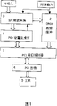
Fig. 1 is the structure of program identifier filter of the present invention.As shown in Figure 1, program identifier of the present invention is crossed and is expressed device and comprise: data acquisition module 0, the program identifier that links to each other with data acquisition module 0 was provided with and expressed operational module 1 and data buffering module 2 respectively, with program identifier the bus control unit module 3 that filter operation module 1 links to each other with data buffering module 2 is set, bus control unit module 3 links to each other with main frame 5 by peripheral element extension interface (PCI) bus 4.
As above-mentioned structure, PID filter of the present invention is to use very high speed IC hardware description (VHDL) to realize in the programmable gate array (FPGA) at the scene.Can solidify very easily, change into application-specific IC (ASIC).Adopted figure to combine in design, design from top to bottom with language.Whole design can be divided into top layer and two levels of bottom.Top layer is the modular structure figure of graphics mode, as shown in Figure 1.Bottom can be described as very high speed IC hardware description (VHDL) code of each module, is sub modular structure, as shown in Figure 2.
Described top layer is:
As shown in Figure 1, main frame 5 (Control Software is contained in inside) by peripheral element extension interface (PCI) bus 4 and (PCI) bus control unit module 3 pre-configured program identifiers filter operation module 1 is set, comprise PID tabulation, filtered model etc.Data acquisition module 0 (synchronous parallel interface (SPI)) and program identifier are provided with and filter behaviour's module 1, data buffering module 2 links to each other, and the data of importing are come in by synchronous parallel interface (SPI) collection, give module 1 after extracting PID; Module 1 according to pre-configured information relatively by PTD, the output control signal is used for data flow in the control module 0.Cushion if need just be input in the module 2; Otherwise, be that unit abandons with the bag data.Module 2 links to each other with module 3, and sends direct memory access (DMA) interruption application and response burst transfer by direct memory access (DMA) controller wherein.And module 3 is controllers of having realized a PCI (2.2) agreement, be main frame 5 (Control Software) with filter between transfer of data and the control bridge of communicating by letter.Main frame 5 wherein is microprocessor or computer.
Fig. 2 is the structure refinement of the program identifier filter of the present invention of Fig. 1.As shown in Figure 2, comprise data latches submodule 001 in the described data acquisition module 0, the data buffer submodule 002 that links to each other with data latches submodule 001, the interface that links to each other with data buffer submodule 002 (synchronous parallel interface (SPI)) controller submodule 004, the byte counter submodule 003 that is connected with clock and the control switch 005 that link to each other with interface controller submodule 004 respectively.
Described program identifier is provided with filter operation module 1 and comprises random asccess memory submodule 101 (or claiming program identifier random access memory (PID RAM) submodule); Program identifier comparator submodule 103 that links to each other with random asccess memory submodule 101 respectively and configuration interface controller submodule 104; The filtered model controller submodule 105 that links to each other with program identifier comparator submodule 103 with configuration interface controller submodule 104 respectively; The program identifier latch submodule 102 that links to each other with interface controller submodule 004 in the data acquisition module 0 with program identifier comparator submodule 103 respectively.Said program identifier latch submodule 103 links to each other with interface controller submodule 004 in the data acquisition module 0; Program identifier comparator submodule 103 links to each other with control switch 005 in the data acquisition module 0.
The pushup storage 202 that comprises data counter submodule 201 and link to each other with clock in described and the data buffering module 2 that data acquisition module 0 links to each other with data counter submodule 201.
Described and program identifier are provided with bus control unit module 3 that filter operation module 1 links to each other with data buffering module 2 and comprise bus control unit (PCI) submodule 301 and direct access memory (DMA) controller submodule 302.
The module among above-mentioned Fig. 1, Fig. 2 and the function of submodule are:
● data acquisition module 0 realizes obtaining from synchronous parallel interface (SPI) function of transport stream (TS) data.Data latches submodule 001 utilizes input clock to latch the data of input TS.In the present embodiment, data buffer submodule 002 provides the buffering of two bytes for latched data.Byte counter submodule 003 offers interface controller (SPI) submodule 004 for each TS input byte count.(SPI) byte number that provided in conjunction with byte counter submodule 003 of interface controller submodule 004 is realized data sync according to the SPI interface protocol.
● program identifier is provided with configuration and the controlled function that filter operation module 1 realizes program identifier (PID).101 storages of random asccess memory (PID RAM) submodule need the PID of operation, comprise program identifier (PID) array: " PID
0, PID
1..., PID
n".Program identifier (PID) latch submodule 102 latchs the PID that extracts from current TS.Whether PID stored among PID that PID comparator submodule 103 is more current and the PID RAM meets.Configuration interface controller submodule 104 is realized the interface conversion with pci controller 3, for main frame 5 provides PID operation control channel.As: PID RAM or configuration PID filtered model are set.Filtered model controller submodule 105 switches the PID filtered model according to the control command of main frame 5 (being arranged at the software in the main frame).
● data buffering module 2 realizes the pooling feature of the direct access memory of data (DMA) controller submodule.Data counter submodule 201 is that direct memory access (DMA) interrupts the thresholding counter controller, when data reach thresholding in pushup storage (FIFO) submodule, sends the interruption application to direct memory access (DMA) controller submodule 302.In pushup storage submodule 202, comprise byte (Byte) array: " Byte
0, Byte
1..., Byte
N-1, Byte
n", it provides the transfer of data buffering for dma controller submodule 302.
● pci bus controller module 3 realizes the controlled function of pci interface and dma controller submodule 302.Pci bus controller submodule 301 is according to the standard of PCI, realizes communicating by letter and the DMA control transmission of data between filter and the main frame (computer or microprocessor).
Described bottom-layer design is:
Digital phase-locking storage submodule 001 in the ■ module 0 has used 8 latchs of the standard in the field programmable gate array (FPGA), latchs TS by input clock, sends into the digit buffer submodule 002 that is made of 16 bit registers.Byte counter submodule 003 also has been to use 8 unidirectional counters of standard in the field programmable gate array (FPGA).Synchronous parallel interface (SPI interface) controller submodule 004 has then used the mode of hardware state machine in conjunction with combinational logic, realizes the extraction of data synchronization and PID according to the requirement of SPI agreement.
■ module 1: be that to form a capacity by the inner random-access memory (ram) of field programmable gate array (FPGA) be 13 * 32 synchronous dual-port random asccess memory (RAM) submodule 101, be used for the PID tabulation that the storing driver setting gets off, and store positive and negative two kinds of filtered models respectively by the filtered model controller submodule 105 that 2 bit registers constitute.The PID of current TS bag obtains from module 0 by the program identifier latch submodule 102 of one 13 standard latch formation, and by program identifier (PID) tabulation among program identifier comparator submodule 103 traversal random asccess memory submodules 101 (the PID RAM), compare with current PID, see whether be consistent, at last according to the different different switch controlling signal of filtered model output in the filtered model controller submodule 105, be used for control data reception with abandon.
■ module 2: be the data buffering of direct memory access (DMA) controller submodule 302.This module mainly is the data buffering that enough sizes are provided for dma controller submodule 302, and can in time send the interrupt requests of data to dma controller.10 unidirectional counters of a standard in this module, have been used equally.And inner (piece) random-access memory (ram) resource of field programmable gate array (FPGA) has also been adopted in the realization of pushup storage submodule 202 (FIFO), is the synchronous pushup storage (FIFO) of a capacity 8 * 512.Data on one side at counting, when data are accumulated to when reaching certain thresholding, are sent to dma controller submodule 302 and are interrupted application when filling FIFO.
■ module 3: this is a peripheral element extension interface (PCI) controller module.It comprises a dma controller submodule 302.In the present embodiment, dma controller submodule 302 utilizes the internal resource of field programmable gate array (FPGA) to realize a controller of following the standard of PCI 2.2 agreements, in order to realize communicating by letter between filter and the main frame.
As above-mentioned structure, adopted hardware state machine to come the transfer and the conversion of design point among the present invention, realize configuration read-write, memory read-write and the input/output end port read-write of PCI, and realized the identification of port by address decoding.
The course of work of filter of the present invention is: main frame (software) carries out various configurations by pci bus to filter, comprise the presetting of initialization, PID RAM of filter, setting of PID filtered model or the like, pci bus controller in the filter (module 3) is the order that receives from pci bus 4, through submitting to configuration interface controller (submodule 104) after the conversion, this module can be gone action according to the instruction that drives, as dispose PID RAM (submodule 101), main frame can be opened dma controller, begins to receive the TS data.
Then, module 0 is utilized input clock, according to the SPI interface protocol, extract the PID of current TS in conjunction with byte counter, and realize to the TS packet synchronously, last program identifier is provided with filter operation module 1 output control switch signal, submits corresponding TS bag on request to.
This concrete workflow of invention filter is described below: submodule 001 is delivered to buffering in the submodule 002 after utilizing the clock of input that the TS that imports is sampled, latchs.Meanwhile, byte counter (submodule 003) is counted each byte data that latchs into, the data of buffering in the count value of submodule 004 zygote module 003 and the submodule 002, standard by digital video broadcasting (DVB) is carried out data sync, and the PID that extracts in the current data stream delivers to module 1; Module 1 latchs current PID by submodule 102, compare by the PID that pre-sets in submodule 103 and the submodule 101, and, judge whether current program data needs to receive, and exports a switch controlling signal at last according to the filtered model control signal of submodule 105.The switch of control data passage, unwanted data are dropped, and the data that need then are transported to data buffering module 2 by the integral multiple of TS bag.
Next, data after counter (submodule 201) reaches the thresholding of DMA, are sent interrupt requests to dma controller (submodule 302) in FIFO (submodule 202) buffering; After request was by response, dma controller was initiated burst transfer by pci bus, data is sent in the middle of the internal memory of main frame.
At last, main frame obtains data from internal memory, to submitting data to application program after data (program identifier) the comparisons Treatment Analysis, or filter is reconfigured, to reach best performance.
The PID filter of the invention described above can be described as a kind of PCI equipment, is to drive and control by the software in the main frame.
The control method of program identifier filter of the present invention be adopt the software be arranged in the main frame to the driving of program identifier filter with control and different filtered models is set.Its concrete control method is:
The first step, at first be initialization, comprise initialization, reset each module to the PID filter.For example for:
The initialization of ▲ module 0: the lowest order to logic reset register (interface on interface bus and the main frame-I/O port, offset address are 0x94) writes ' 1 ', writes ' 0 ' again after 10 milliseconds at least at interval.This operation meeting resets to all submodules in the module 0: byte counter is cleared, and buffer is cleared, and latch and SPI interface controller are reset, and control switch is disconnected;
The initialization of ▲ module 1: the lowest order to logic reset register (I/O port, offset address are 0x94) writes ' 0 ', writes ' 1 ' again after 10 milliseconds at least at interval.This operation can empty the PID RAM submodule in the module 1, and other submodule is resetted;
The initialization of ▲ module 2: the lowest order to logic reset register (I/O port, offset address are 0x94) writes ' 1 ', writes ' 0 ' again after 10 milliseconds at least at interval.This operates meeting to the counter submodule zero clearing in the module 2, and empties FIFO;
The initialization of ▲ module 3: the highest order of logic reset register (I/O port, offset address are 0x00) is write ' 1 ', write ' 0 ' again after 10 milliseconds at least at interval.This operation meeting resets to module 3.
Second goes on foot, is provided with the filtered model of program identifier (PID) filter:
1, the positive logic filtered model is set earlier: lowest order in the PID mode register (I/O port, offset address are 0x8C) is write ' 0 '; This moment, the PID filter was in the positive logic operating state, received only the corresponding TS data with set PID.
2, the antilogical filtered model is set again: lowest order in the PID mode register (I/O port, offset address are 0x8C) is write ' 1 '; This moment, the PID filter was in the antilogical operating state, received only the every other TS data except that the corresponding TS data of set PID.
The 3rd goes on foot, is provided with the program identifier (PID) of PID filter:
1, the modification to program identifier (PID) is operated by elder generation: at PID serial number register (I/O port, offset address is 0x84) in write the sequence number of the PID that need to revise, write the numerical value of revising back PID at PID numerical value register (IO port, offset address are 0x88).PID numerical value on the correspondence position in PID RAM is modified like this.If will delete single PID, only need in the PID serial number register, write corresponding PID sequence number, and write the numerical value (0x1FFF) of PID at PID numerical value register, get final product;
2, operate emptying other PID among the PID RAM again: lowest order writes ' 1 ' in PID reseting register (I/O port, offset address are 0x90), and then writes ' 0 '.All locational PID will be cleared among the PID RAM at this moment;
The 4th step, starting PID filter receive data:
At first the log-on data receive path writes ' 1 ' at the middle lowest order of logic control register (I/O port, offset address are 0x9C).At this moment, when the data among the FIFO reached thresholding, hardware can be initiated the DMA transmission, and data can be sent in the corresponding DMA internal memory;
Then obtain the data that received, after transfer of data is finished, can produce a DMA and interrupt, and from DMA internal memory, can obtain data corresponding address;
The form of the 5th step, analysis PID filter: analyze the program identifier and the program category of all programs that Program Map Table provided of Program Association Table acquisition, therefrom draw the number of program identifier and the data traffic of every class program.
In standard DVB system, can comprise the packet that some indicate specific PID in the transport stream, be commonly referred to special form, the important information on services of some relevant these transport stream can be provided in these special forms.Wherein importantly the most frequently used be:
Program Association Table (PAT) is (PID=0x00)---and be at each multiplexing road business, provide corresponding Program Map Table (PMT) and network information table (NIT) corresponding PID.
Program Map Table (PMT)-be the PID of program clock reference (PCR) the field correspondence of sign and the every road of the PID business of indicating the stream correspondence of forming every road business, and the program category of every road business.
Therefore, PID=0x00 is set, and the corresponding data of reception just can obtain complete Program Association Table (PAT).Be easy to just can know the pairing PID of Program Map Table (PMT) by the information that provides among the PAT, so just can arrive the PMT Data Receiving, form complete PMT.And PMT can provide the PID and the program category of all programs, therefrom just can draw the number of PID and the data traffic that estimates every class program.
Fig. 3 is the idiographic flow to the above-mentioned control method of filter of the present invention.According to the flow process of Fig. 3, the concrete steps of the invention described above control method are:
The first step: initialization, each module of filter is carried out reset operation, and PCI allocation bus control unit submodule, direct memory access (DMA) or the like is set;
Second step: by peripheral element extension interface (PCI) bus I/O port, be configured the interface controller module, filtered model controller submodule is set, make it be in the positive logic operating state;
The 3rd step:, be configured the interface controller submodule, 00 by pci bus I/O port, 01,10,11 four program identifiers (hexadecimal) write in program identifier random asccess memory (PID RAM) submodule 101, and empty other program identifier (PID);
The 4th step: configuration direct memory access (DMA) controller submodule, open the Data Receiving switch, the log-on data receive path; Data directly are sent in the corresponding internal memory of main frame by direct memory access (DMA) controller submodule;
The 5th step: from host memory, obtain data and analyze form, obtain the corresponding program identifier (PID) of Program Map Table (PMT); The PID that table (PMT) is corresponding writes in joint random asccess memory (PID RAM) submodule, and empties other program identifier (PID);
The 7th step: from host memory, obtain data and analyze form, can obtain in the transport stream the multiplexing program identifier (PID) that must be all of institute, and program category accordingly;
The 8th step: the quantity N of (PID) of the program correspondence that analysis user need receive, and corresponding data flow amount.If quantity N≤32 of program correspondence then jumped to for the 9th step; Otherwise, jumped to for the tenth step;
The 9th step: keep the positive logic filtered model constant,, be configured the interface controller submodule, all PID of required reception are write PID RAM, and empty other PID by pci bus I/O port.Then, jumped to for the 12 step;
The tenth step: by pci bus I/O port, be configured the interface controller submodule filtered model controller submodule is set, make it be in the antilogical operating state;
The 11 step: pairing PID writes PID RAM the program that does not need to receive, if the PID number more than or equal to 32, then selects 32 bigger PID of flow to write PID RAM.If the PID number less than 32, then all writes PID RAM to them, and empties the PID on the rest position among the PID RAM;
The 12 step: restart the Data Receiving passage, configuration finishes.