WO2025142145A1 - 光検出装置、光検出装置の製造方法及び電子機器 - Google Patents
光検出装置、光検出装置の製造方法及び電子機器 Download PDFInfo
- Publication number
- WO2025142145A1 WO2025142145A1 PCT/JP2024/039692 JP2024039692W WO2025142145A1 WO 2025142145 A1 WO2025142145 A1 WO 2025142145A1 JP 2024039692 W JP2024039692 W JP 2024039692W WO 2025142145 A1 WO2025142145 A1 WO 2025142145A1
- Authority
- WO
- WIPO (PCT)
- Prior art keywords
- light
- line width
- depth
- region
- semiconductor layer
- Prior art date
- Legal status (The legal status is an assumption and is not a legal conclusion. Google has not performed a legal analysis and makes no representation as to the accuracy of the status listed.)
- Pending
Links
Images
















Classifications
-
- H—ELECTRICITY
- H10—SEMICONDUCTOR DEVICES; ELECTRIC SOLID-STATE DEVICES NOT OTHERWISE PROVIDED FOR
- H10F—INORGANIC SEMICONDUCTOR DEVICES SENSITIVE TO INFRARED RADIATION, LIGHT, ELECTROMAGNETIC RADIATION OF SHORTER WAVELENGTH OR CORPUSCULAR RADIATION
- H10F39/00—Integrated devices, or assemblies of multiple devices, comprising at least one element covered by group H10F30/00, e.g. radiation detectors comprising photodiode arrays
- H10F39/10—Integrated devices
- H10F39/12—Image sensors
-
- H—ELECTRICITY
- H10—SEMICONDUCTOR DEVICES; ELECTRIC SOLID-STATE DEVICES NOT OTHERWISE PROVIDED FOR
- H10F—INORGANIC SEMICONDUCTOR DEVICES SENSITIVE TO INFRARED RADIATION, LIGHT, ELECTROMAGNETIC RADIATION OF SHORTER WAVELENGTH OR CORPUSCULAR RADIATION
- H10F39/00—Integrated devices, or assemblies of multiple devices, comprising at least one element covered by group H10F30/00, e.g. radiation detectors comprising photodiode arrays
- H10F39/10—Integrated devices
- H10F39/12—Image sensors
- H10F39/18—Complementary metal-oxide-semiconductor [CMOS] image sensors; Photodiode array image sensors
Definitions
- microloading When processing deep trench shapes such as through trenches and non-through trenches, or when processing by dry etching, a phenomenon occurs in which the processing depth varies depending on the processing pattern, i.e., microloading. This microloading phenomenon increases the difficulty of process design in order to ensure light-shielding performance. Also, in the case of a through trench structure, the microloading phenomenon makes it impossible to ensure a break margin to the lower layer. Furthermore, in a structure in which a photodiode and a MEM (memory) are stacked vertically, the light-shielding band width increases depending on the microloading thickness, creating issues from the perspective of pixel design.
- MEM memory
- Patent Document 1 discloses an image sensor that reduces the microloading phenomenon by arranging an isolation region that isolates multiple pixels from each other and forming a non-isolation region at the corner of the pixel.
- the image sensor disclosed in Patent Document 1 removes the orthogonal portions in order to avoid processing depth variations that occur at the orthogonal portions where processing patterns overlap when processing light-shielding trenches between photoelectric conversion elements.
- One aspect of the present disclosure is a photodetector device comprising: a semiconductor layer having a light-receiving surface on which light is incident and an element-forming surface located on the opposite side of the light-receiving surface; a plurality of pixels arranged in a matrix on the semiconductor layer and capable of generating an electrical signal in response to light incident from the light-receiving surface; and a pixel separator extending in a depth direction from the light-receiving surface of the semiconductor layer to the element-forming surface and separating adjacent pixels, the pixel separator extending in a row direction or a column direction in a plan view, a recessed region having a first depth formed with a first line width, and a recessed region having a second depth different from the first depth formed with a second line width different from the first line width so as to match the recessed region of the first depth.
- Another aspect of the present disclosure is a method for manufacturing a photodetector comprising: a semiconductor layer having a light-receiving surface on which light is incident and an element forming surface located on the opposite side of the light-receiving surface; a plurality of pixels arranged in a matrix on the semiconductor layer and capable of generating an electrical signal in response to light incident from the light-receiving surface; and a pixel separation section extending in a depth direction from the light-receiving surface of the semiconductor layer to the element forming surface and separating adjacent pixels, the method comprising the steps of: forming a recessed region having a first depth of the pixel separation section extending in a row direction or a column direction in a plan view, the ...
- a method for manufacturing a photodetector comprising: forming a recessed region having a second depth different from the first depth, forming a recessed region having a second line width different from the first line width so as to match the recessed region of the first depth, forming a buried film in the recessed region, forming a hard mask opening pattern in a recessed region having a line width greater than the first line width, and removing the buried film in the recessed region based on the hard mask opening pattern.
- an electronic device including a photodetector device comprising: a semiconductor layer having a light-receiving surface on which light is incident and an element forming surface located on the opposite side of the light-receiving surface; a plurality of pixels arranged in a matrix in the semiconductor layer and capable of generating an electrical signal in response to light incident from the light-receiving surface; and a pixel separator extending in a depth direction from the light-receiving surface of the semiconductor layer to the element forming surface and separating adjacent pixels, the pixel separator extending in a row direction or a column direction in a plan view, a recessed region having a first depth formed with a first line width, and a recessed region having a second depth different from the first depth formed with a second line width different from the first line width so as to match the recessed region of the first depth.
- FIG. 1 is a chip layout diagram showing a configuration example of a photodetector according to a first embodiment of the present disclosure.
- 1 is a block diagram showing a configuration example of a light detection device according to a first embodiment of the present disclosure.
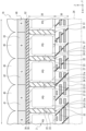
- 2 is a schematic cross-sectional view showing a cross-sectional structure of a pixel array portion.
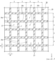
- FIG. 2 is a schematic plan view showing a plane pattern of an isolation region in a pixel array portion;
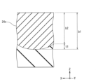
- FIG. FIG. 13 is a plan view of a straight pattern of an isolation region in a comparative example of the first embodiment.
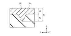
- 5B is a cross-sectional view of a linear pattern of the separation region shown by the dashed line in FIG. 5A.
- FIG. 11 is a plan view of a crossing pattern of isolation regions in a comparative example of the first embodiment.
- 6B is a cross-sectional view of the crossing pattern of the isolation regions shown by the dashed dotted line in FIG. 6A.
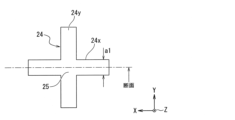
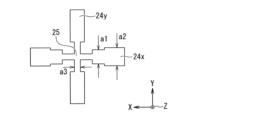
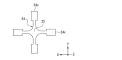
- FIG. 2 is a plan view of a crossing pattern of isolation regions in the first embodiment of the present disclosure.
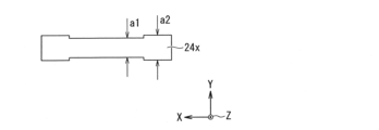
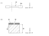
- FIG. 2 is a plan view of a linear pattern of an isolation region in the first embodiment of the present disclosure.
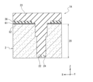
- 4 is a cross-sectional view showing an example of a structure of a stopper layer for a trench in the first embodiment of the present disclosure.
- FIG. FIG. 2 is a plan view (part 1) showing a process of forming an active pattern from a trench pattern in the first embodiment of the present disclosure.
- FIG. 4 is a plan view (part 2) showing a process of forming an active pattern from a trench pattern in the first embodiment of the present disclosure.
- FIG. 11 is a plan view (part 3) showing a process of forming an active pattern from a trench pattern in the first embodiment of the present disclosure.
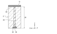
- 5A to 5C are cross-sectional views (part 1) illustrating process steps of a method for forming an isolation region and an element isolation portion of the photodetector according to the first embodiment of the present disclosure.
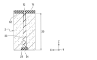
- 5A to 5C are cross-sectional views (part 2) illustrating process steps of the method for forming an isolation region and an element isolation portion of the photodetector according to the first embodiment of the present disclosure.
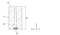
- 5A to 5C are cross-sectional views (part 3) illustrating process steps of a method for forming an isolation region and an element isolation portion of a photodetector according to the first embodiment of the present disclosure.
- 5A to 5C are cross-sectional views (part 4) illustrating process steps of the method for forming an isolation region and an element isolation portion of the photodetector according to the first embodiment of the present disclosure.
- 5A to 5C are cross-sectional views showing process steps of a method for forming an isolation region and an element isolation portion of a photodetector according to the first embodiment of the present disclosure
- 10A to 10C are cross-sectional views (part 1) illustrating a process procedure of a method for backfilling an insulating film in an isolation region of a photodetector according to a first modified example of the first embodiment of the present disclosure with a metal film.
- 11A to 11C are cross-sectional views (part 2) illustrating a process procedure of a method for backfilling an insulating film in an isolation region of a photodetector according to a first modified example of the first embodiment of the present disclosure with a metal film.
- 11A to 11C are cross-sectional views (part 3) illustrating a process procedure of a method for backfilling an insulating film in an isolation region of a photodetector according to a first modified example of the first embodiment of the present disclosure with a metal film.
- 11A to 11C are cross-sectional views (part 4) illustrating the process steps of the method of backfilling the insulating film in the isolation region of the photodetector according to the first modified example of the first embodiment of the present disclosure with a metal film.
- FIG. 11 is a plan view showing an example of a hole arrangement pattern in a first modified example of the first embodiment of the present disclosure.
- FIG. 13 is a plan view showing a state in which the opening area of a corner portion at an intersection of isolation regions is increased due to lithography, as a comparative example of the second modified example of the first embodiment of the present disclosure.
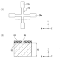
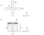
- 11A and 11B are a plan view and a cross-sectional view (part 1) illustrating a process procedure of a method for forming an intersection point of isolation regions in a photodetector device according to a second modified example of the first embodiment of the present disclosure.
- 11A and 11B are a plan view and a cross-sectional view (part 2) showing a process procedure of a method for forming an intersection point of isolation regions in a photodetector device according to a second modified example of the first embodiment of the present disclosure.
- FIG. 11A and 11B are plan views and cross-sectional views (part 3) showing a process procedure of a method for forming an intersection point of isolation regions in a photodetector device according to a second modified example of the first embodiment of the present disclosure.
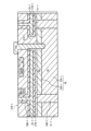
- FIG. 11 is a partial cross-sectional view illustrating an example of a light detection device according to a second embodiment of the present disclosure.
- 11A to 11C are cross-sectional views (part 1) illustrating an example of a manufacturing process for a light detection device according to a second embodiment of the present disclosure.
- 13A to 13C are cross-sectional views (part 2) illustrating an example of a manufacturing process for the light detection device according to the second embodiment of the present disclosure.
- 13A to 13C are cross-sectional views (part 3) illustrating an example of a manufacturing process for the light detection device according to the second embodiment of the present disclosure.
- 13A to 13C are cross-sectional views (part 4) illustrating an example of a manufacturing process for a light detection device according to a second embodiment of the present disclosure.
- 5 is a cross-sectional view (part 5) illustrating an example of a manufacturing process for the light detection device according to the second embodiment of the present disclosure.
- FIG. 6 is a cross-sectional view (part 6) illustrating an example of a manufacturing process for the light detection device according to the second embodiment of the present disclosure.
- the semiconductor chip 2 includes a semiconductor layer 20 having a plurality of photoelectric conversion regions 27, and a color filter layer 40 arranged on the light incident surface side, which is the second surface S2 side of a first surface S1 and a second surface S2 located opposite each other in the thickness direction (Z direction) of the semiconductor layer 20.
- the semiconductor chip 2 further includes a plurality of microlenses 45 (on-chip lenses, wafer lenses) arranged on the light incident surface side of the color filter layer 40 (the side opposite to the semiconductor layer 20 side).
- the semiconductor chip 2 further includes a multilayer wiring layer 30 arranged on the first surface S1 side of the semiconductor layer 20, and a support substrate 34 arranged on the side of the multilayer wiring layer 30 opposite the semiconductor layer 20 side.
- the support substrate 34 is provided on the surface of the multi-layer wiring layer 30 opposite the surface facing the semiconductor layer 20.
- the support substrate 34 is a substrate for ensuring the strength of the semiconductor layer 20 during the manufacturing stage of the light detection device 1A.
- the material for the support substrate 34 may be, for example, silicon (Si).
- a planarization film 36 and an adhesive film 38 are laminated in this order from the semiconductor layer 20 side between the semiconductor layer 20 and the color filter layer 40.
- the planarization film 36 covers the entire light incident side of the semiconductor layer 20 in the pixel array section 2A so that the light incident side of the semiconductor layer 20 is a flat surface without any irregularities.
- the planarization film 36 may be, for example, a silicon oxide (SiO2) film.
- the adhesive film 38 is disposed between the planarization film 36 and the color filter layer 40.
- a silicon oxide film is used as the adhesive film 38.
- the photodetector 1A having the above configuration, light is irradiated from the microlens 45 side of the semiconductor chip 2, the irradiated light passes through the microlens 45 and the color filter sections 41, 42, and 43 individually, and the transmitted light is photoelectrically converted in the photoelectric conversion region 27 to generate signal charges.
- the generated signal charges are then output as pixel signals by the vertical signal lines 11 consisting of the wiring 32 of the multilayer wiring layer 30 via pixel transistors formed on the first surface S1 side of the semiconductor layer 20.
- the distance to the subject is calculated based on the difference between the signal charges generated in the photoelectric conversion region 27.
- the separation region 24 includes a first portion 24x that extends in the X direction with a line width a1 in a plan view, and a second portion 24y that extends in the Y direction.
- the first portion 24x and the second portion 24y extend in directions perpendicular to each other.
- Each of the photoelectric conversion regions 27 is partitioned at both ends in the X direction by two second portions 24y of the separation region 24, and at both ends in the Y direction by two first portions 24x of the separation region 24.
- Each of the first portion 24x and the second portion 24y included in the separation region 24 extends across the second surface and the first surface of the semiconductor layer 20.
- Each of the first portion 24x and the second portion 24y includes a trench 22 that extends across the second surface S2 and the first surface S1 of the semiconductor layer 20, and an insulating film 23 embedded in the trench 22.
- Fig. 5A is a plan view of the straight pattern of the separation region 24 in a comparative example of the first embodiment.
- Fig. 5B is a cross-sectional view of the straight pattern of the separation region 24 indicated by the dashed line in Fig. 5A.
- both ends of the straight pattern have a depth b2 that is shallower by t1 than the depth b1 at the center of the straight pattern due to the microloading phenomenon. Therefore, the separation region 24 becomes non-penetrating, so that light leaks in and the light blocking property is deteriorated.
- FIG. 6A is a plan view of the intersection pattern of the isolation region 24 in a comparative example of the first embodiment.
- FIG. 6B is a cross-sectional view of the intersection pattern of the isolation region 24 indicated by the dashed line in FIG. 6A.
- the depth b3 of the intersection point between the first portion 24x and the second portion 24y of the isolation region 24 (hereinafter referred to as the intersection point 25) is deeper by t2 than the depth b1 of the non-intersection point due to the microloading phenomenon. For this reason, there is a risk that the isolation region 24 will damage the lower layer, exposing the metal of the multilayer wiring layer 30.
- Fig. 7 is a plan view of a cross pattern of the separation region 24 in the first embodiment of the present disclosure.
- Fig. 8 is a plan view of a straight pattern of the separation region 24 in the first embodiment of the present disclosure.
- the line width a3 of the intersection 25 between the first portion 24x and the second portion 24y of the isolation region 24 is made thinner than the line width a1 of the non-intersection, and the depth b3 of the intersection 25 is made to match the depth b1 of the non-intersection.
- the area of the location where the microloading phenomenon occurs corresponds to the area of the processed location of the isolation region 24.
- the line width a2 at both ends of the intersection pattern is made thicker than the line width a1. Note that the range where the line width is made thinner and thicker than a1 is the range where an insulating film 23 such as silicon oxide (SiO2) can be embedded in the trench 22 of the isolation region 24.
- the line width a2 at both ends of the straight line pattern of the separation region 24 is formed to be thicker than the line width a1, and the depth b2 at both ends is made to match the depth b1.
- FIGS. 10A to 10C are plan views showing the process of forming an active pattern from a trench pattern.
- the process for forming the isolation region 24 can be performed not only at a process position after the back surface of the back-illuminated image sensor is turned to the back surface, but also at a FEOL (Front End Of Line) process for forming transistors and the like.
- FEOL Front End Of Line
- the photodetector 1A is manufactured using various devices such as a film forming device (including a CVD (Chemical Vapor Deposition) device and a sputtering device), an ion implantation device, a heat treatment device, an etching device, a CMP (Chemical Mechanical Polishing) device, and a bonding device.
- a film forming device including a CVD (Chemical Vapor Deposition) device and a sputtering device
- an ion implantation device including a heat treatment device, an etching device, a CMP (Chemical Mechanical Polishing) device, and a bonding device.
- these devices are collectively referred to as manufacturing devices.
- the manufacturing equipment removes the insulating film 23 covering the top surface of the planarization film 36 in an etch-back process. Then, in FIG. 11C, the manufacturing equipment deposits, for example, a coating film 62 in the area in the trench 22 where the insulating film 23 has been removed.
- the coating film 62 is a fluid film-forming material formed by a coating process or the like.
- the manufacturing equipment forms an anti-reflective film 63 on the upper surface of the planarization film 36 and the upper surface of the coating film 62, and then patterns a resist 64 on the anti-reflective film 63 in a lithography process.
- the resist 64 is formed in the region of the line width a2 of the isolation region 24, and a hard mask opening pattern is arranged.
- the line width is made wider in the portion where the trench 22 is shallower, and the line width is made narrower in the portion where the trench 22 is deeper, thereby making it possible to control the microloading phenomenon. Therefore, by mitigating the influence of the microloading phenomenon, freedom in the potential design of the structures of the pixels 3 and the photoelectric conversion region 27 can be obtained, and the characteristics can be improved.
- the isolation region 24 is first flattened, and a hard mask opening pattern is placed in the thick line width area of the isolation region 24, and the active pattern 54 is formed by overlapping it with the isolation region 24, thereby making it possible to avoid characteristic degradation.
- a first modified example of the first embodiment of the present disclosure relates to removing the insulating film 23 in the trench 22 after the back surface is formed in the FEOL process and backfilling with a metal film.
- a metal film that is expected to have high light shielding properties cannot be used from the viewpoint of contamination, and an insulating film 23 such as silicon oxide SiO2 or Poly-Si is filled in. Therefore, when the isolation region 24 is formed in the FEOL process, in order to fill the trench 22 of the isolation region 24 with a metal film, it is necessary to remove the insulating film 23 in the trench 22 after the back surface is formed and backfill with a metal film.
- Method of manufacturing a photodetector 12A to 12D are cross-sectional views showing the process steps of a method for backfilling the insulating film 23 in the isolation region 24 of the photodetector 1A in the first modified example of the first embodiment of the present disclosure with a metal film.
- the manufacturing equipment removes the insulating film 23 buried in the trench 22 by a wet etching process. Then, in FIG. 12D, the manufacturing equipment removes the resist 71.
- the above-mentioned hole 72 is placed at the intersection 25 of the first portion 24x and the second portion 24y of the isolation region 24, taking into consideration misalignment of the etching pattern of the insulating film 23.
- thinning the intersection 25 deteriorates the alignment margin. Therefore, in a first modified example of the first embodiment of the present disclosure, as shown in FIG. 13, the hole 72 is placed in the regions 24x1 and 24x2 that correspond to the line width a1 of the first portion 24x of the isolation region 24.
- the hole 72 is placed in the regions 24y1 and 24y2 that correspond to the line width a1 of the second portion 24y of the isolation region 24. This relaxes design constraints.
- the second modified example of the first embodiment of the present disclosure is a measure to address the problem of microloading being deteriorated due to the opening area of the corner portion of the intersection 25 of the isolation region 24 becoming larger due to lithography, as shown in FIG.
- the manufacturing equipment deposits a resist 81 as a hard mask on the second surface S2 of the semiconductor layer 20 in order to form the first portion 24x of the isolation region 24 in a lithography process.
- the manufacturing equipment then forms an opening 82 in the first portion 24x of the isolation region 24 along the direction indicated by the arrow X in FIG. 15A.
- the manufacturing equipment removes silicon from the semiconductor layer 20 along the openings 82 and 83 using a wet etching process or the like to form trenches 22.
- the photodetector 1B is, for example, a global shutter back-illuminated image sensor formed of a complementary metal oxide semiconductor (CMOS) image sensor or the like.
- CMOS complementary metal oxide semiconductor
- the first substrate 30-1 is constructed by laminating an insulating layer 32-1 on a semiconductor substrate 31-1 (an example of a semiconductor layer). In other words, the insulating layer 32-1 is formed in contact with the upper surface of the semiconductor substrate 31-1.
- the first transfer transistor TRX, the second transfer transistor TRM, the charge holding unit MEM, the third transfer transistor TRG, the floating diffusion FD, and the discharge transistor OFG are formed on the upper surface of the semiconductor substrate 31-1.
- the charge holding unit MEM is formed near the upper surface of the semiconductor substrate 31-1. Therefore, the upper surface of the semiconductor substrate 31-1 serves as the formation surface 31B-1 for the first transfer transistor TRX and the like.
- the gate electrodes of the first transfer transistor TRX, the second transfer transistor TRM, the third transfer transistor TRG, and the discharge transistor OFG, and the wiring connected to these gate electrodes are provided.
- the gate electrodes of the first transfer transistor TRX, the second transfer transistor TRM, the third transfer transistor TRG, and the discharge transistor OFG, and the wiring connected to these gate electrodes are formed, for example, from a metal material.
- the gate electrode (vertical gate electrode VG) of the first transfer transistor TRX may be formed from polysilicon.
- the gate electrode (vertical gate electrode VG) of the first transfer transistor TRX is formed extending from the upper surface (forming surface 31B-1) of the semiconductor substrate 31-1 in the thickness direction (normal direction) of the semiconductor substrate 31-1.
- the gate electrode (vertical gate electrode VG) of the first transfer transistor TRX extends from the formation surface 31B-1 to a depth that reaches the N-type semiconductor region 32A (photodiode PD).
- the gate electrode (vertical gate electrode VG) of the first transfer transistor TRX has, for example, a rod-like shape that extends in the thickness direction (normal direction) of the semiconductor substrate 31-1.
- the element isolation section 34-1 is formed so as to surround the pixel 11-1 (particularly the photodiode PD) in the horizontal plane direction, and is further formed extending in the normal direction (thickness direction) of the semiconductor substrate 31-1.
- the element isolation section 34-1 is formed between two adjacent photodiodes PD.
- the element isolation section 34-1 is composed of, for example, a metal embedded section 34A-1 and a P-type semiconductor section 34B-1.
- the metal-embedded portion 37A-1 is formed, for example, by using CVD.
- the metal-embedded portion 37A-1 is formed, for example, of aluminum or an aluminum alloy.
- the insulating film 37B-1 is, for example, an oxide film formed by thermally oxidizing the semiconductor substrate 31-1, and is formed, for example, of silicon oxide.
- the insulating film 37B-1 may be composed of a multilayer film including a SiO2 film (silicon oxide film).
- the insulating film 37B-1 may have a layered structure composed, for example, of a SiO2 film (silicon oxide film), an SCF film, and a SiO2 film (silicon oxide film).
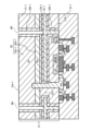
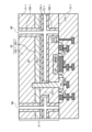
- Figures 17A to 17L show an example of a manufacturing process for the light detection device 1B.
- a semiconductor substrate 31-1 is prepared on which a photodiode PD, a P-type semiconductor portion 34B-1, a floating diffusion FD, a charge storage portion MEM, etc. are formed (FIG. 17A).
- a hard mask 110-1 is formed on the upper surface (formation surface 31B-1) of the semiconductor substrate 31-1 to selectively cover the formation surface 31B-1 (FIG. 17A).
- the hard mask 110-1 has an opening H1 at the position where the element isolation portion 36-1 is to be formed, and is made of an insulating material such as SiN (silicon nitride) or SiO2 (silicon oxide).
- the portion of the Si (111) that constitutes the semiconductor substrate 31-1 exposed at the opening H1 is dug down by dry etching using the hard mask 110-1 to form a trench H2 at the position where the element isolation section 36-1 is to be formed (FIG. 17B).
- the depth of the trench H2 at this time corresponds to the dimension in the depth direction of the element isolation section 36-1 that will be formed later. Note that when wet etching is performed on the semiconductor substrate 31-1, which will be described later, the etching process also progresses slightly in the ⁇ 111> direction, so it is advisable to adjust the depth of the trench H2 taking this into consideration.
- sidewalls 33s-1 are formed to cover the sides of trench H2 (FIG. 17C).
- an insulating film made of, for example, SiN or SiO2 is formed to cover the inner surface of trench H2, i.e., the sides and bottom of trench H2, and then only the insulating film covering the bottom of trench H2 is removed by dry etchback.
- a cavity 51-1 is formed inside the semiconductor substrate 31-1, which is a Si (111) substrate, surrounded by crystal surfaces 31D-1, 31E-1, and 31F-1, and communicating with trench H2 (FIG. 17E).
- the semiconductor portion 31C is formed in the same layer of the semiconductor substrate 31-1 as the cavity portion 51-1.
- a trench H4 is formed in the P-type semiconductor portion 34B-1 from the light receiving surface 31A-1 side of the semiconductor substrate 31-1 using, for example, dry etching (FIG. 17J).
- the trench H4 is formed to a depth where the bottom surface of the trench H4 reaches the buried portion 35-1.
- the buried portion 35-1 is removed by wet etching using a specified chemical solution.
- a cavity portion 53-1 that spreads in the stacking plane direction and connects to the trench H4 is formed at the position where the buried portion 35-1 was removed (FIG. 17K).
- the chemical solution used at this time is, for example, hydrofluoric acid.
- the insulating film 37B-1 remains without being etched, so the insulating film 37B-1 remains between the vertical gate electrode VG and the cavity portion 53-1.
- metal embedded portions 34A-1, 36A-1, and 37A-1 are formed by, for example, CVD so as to fill trench H4 and cavity 53-1 (FIG. 17L).
- the surface is then flattened by surface polishing using CMP.
- second substrate 40-1 is bonded to light receiving surface 31A-1 of semiconductor substrate 31-1, and light receiving lens 50-1 is bonded to light receiving surface 31A-1.
- photodetector 1B according to the second embodiment of the present disclosure is manufactured.
- the thickness of the light-shielding portion after wet etching increases as the microloading during processing of the trench H2 increases, and the area of the photodiode PD or the charge storage portion (MEM) decreases, so that the thickness can be minimized by changing the line width of the trench H2. This improves the degree of freedom in designing the pixel 11-1.
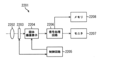
- FIG. 18 is a block diagram showing an example configuration of an imaging device as an electronic device to which the present technology is applied.
- the imaging device 2201 shown in FIG. 18 is configured with an optical system 2202, a shutter device 2203, a solid-state imaging element 2204 as a light detection device, a control circuit 2205, a signal processing circuit 2206, a monitor 2207, and two memories 2208, and is capable of capturing still images and moving images.
- the optical system 2202 is configured to have one or more lenses, and guides light from a subject (incident light) to the solid-state image sensor 2204 , forming an image on the light receiving surface of the solid-state image sensor 2204 .
- the shutter device 2203 is disposed between the optical system 2202 and the solid-state image sensor 2204 , and controls the light irradiation period and light blocking period for the solid-state image sensor 2204 under the control of a control circuit 2205 .
- the solid-state imaging element 2204 is configured by a package including the above-mentioned solid-state imaging element.
- the solid-state imaging element 2204 accumulates signal charge for a certain period of time according to the light that is imaged on the light receiving surface via the optical system 2202 and the shutter device 2203.
- the signal charge accumulated in the solid-state imaging element 2204 is transferred according to a drive signal (timing signal) supplied from the control circuit 2205.
- the control circuit 2205 outputs a drive signal that controls the transfer operation of the solid-state image sensor 2204 and the shutter operation of the shutter device 2203, thereby driving the solid-state image sensor 2204 and the shutter device 2203.
- the technology according to the present disclosure (the present technology) can be applied to various products.
- the technology according to the present disclosure may be applied to an endoscopic surgery system.
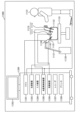
- FIG. 19 is a diagram showing an example of a schematic configuration of an endoscopic surgery system to which the technology according to the present disclosure (the present technology) can be applied.
- 19 shows a state in which an operator (doctor) 11131 is performing surgery on a patient 11132 on a patient bed 11133 using an endoscopic surgery system 11000.
- the endoscopic surgery system 11000 is composed of an endoscope 11100, other surgical tools 11110 such as an insufflation tube 11111 and an energy treatment tool 11112, a support arm device 11120 that supports the endoscope 11100, and a cart 11200 on which various devices for endoscopic surgery are mounted.
- the endoscope 11100 is composed of a lens barrel 11101, the tip of which is inserted into the body cavity of the patient 11132 at a predetermined length, and a camera head 11102 connected to the base end of the lens barrel 11101.
- the endoscope 11100 is configured as a so-called rigid scope having a rigid lens barrel 11101, but the endoscope 11100 may also be configured as a so-called flexible scope having a flexible lens barrel.
- the tip of the tube 11101 has an opening into which an objective lens is fitted.
- a light source device 11203 is connected to the endoscope 11100, and light generated by the light source device 11203 is guided to the tip of the tube by a light guide extending inside the tube 11101, and is irradiated via the objective lens towards an object to be observed inside the body cavity of the patient 11132.
- the endoscope 11100 may be a direct-viewing endoscope, an oblique-viewing endoscope, or a side-viewing endoscope.
- An optical system and an image sensor are provided inside the camera head 11102, and the reflected light (observation light) from the object of observation is focused on the image sensor by the optical system.
- the image sensor converts the observation light photoelectrically to generate an electrical signal corresponding to the observation light, i.e., an image signal corresponding to the observed image.
- the image signal is sent to the camera control unit (CCU: Camera Control Unit) 11201 as RAW data.
- CCU Camera Control Unit
- the light source device 11203 is composed of a light source such as an LED (Light Emitting Diode), and supplies irradiation light to the endoscope 11100 when photographing an operation site, etc.
- the input device 11204 is an input interface for the endoscopic surgery system 11000.
- a user can input various information and instructions to the endoscopic surgery system 11000 via the input device 11204. For example, the user inputs an instruction to change the imaging conditions (type of irradiation light, magnification, focal length, etc.) of the endoscope 11100.
- the light source device 11203 that supplies irradiation light to the endoscope 11100 when photographing the surgical site can be composed of a white light source composed of, for example, an LED, a laser light source, or a combination of these.
- a white light source composed of, for example, an LED, a laser light source, or a combination of these.
- the white light source is composed of a combination of RGB laser light sources, the output intensity and output timing of each color (each wavelength) can be controlled with high precision, so that the white balance of the captured image can be adjusted in the light source device 11203.
- excitation light is irradiated to the body tissue and the fluorescence from the body tissue is observed (autofluorescence observation), or a reagent such as indocyanine green (ICG) is locally injected into the body tissue and excitation light corresponding to the fluorescent wavelength of the reagent is irradiated to the body tissue to obtain a fluorescent image.
- the light source device 11203 may be configured to supply narrow band light and/or excitation light corresponding to such special light observation.
- the lens unit 11401 is an optical system provided at the connection with the lens barrel 11101. Observation light taken in from the tip of the lens barrel 11101 is guided to the camera head 11102 and enters the lens unit 11401.
- the lens unit 11401 is composed of a combination of multiple lenses including a zoom lens and a focus lens.
- the communication unit 11404 is configured with a communication device for transmitting and receiving various information to and from the CCU 11201.
- the communication unit 11404 transmits the image signal obtained from the imaging unit 11402 as RAW data to the CCU 11201 via the transmission cable 11400.
- the communication unit 11404 also receives control signals for controlling the operation of the camera head 11102 from the CCU 11201, and supplies them to the camera head control unit 11405.
- the control signals include information on the imaging conditions, such as information specifying the frame rate of the captured image, information specifying the exposure value during imaging, and/or information specifying the magnification and focus of the captured image.
- the control unit 11413 performs various controls related to the imaging of the surgical site, etc. by the endoscope 11100, and the display of the captured images obtained by imaging the surgical site, etc. For example, the control unit 11413 generates a control signal for controlling the driving of the camera head 11102.
- the control unit 11413 also causes the display device 11202 to display the captured image showing the surgical site, etc., based on the image signal that has been image-processed by the image processing unit 11412. At this time, the control unit 11413 may recognize various objects in the captured image using various image recognition techniques. For example, the control unit 11413 can recognize surgical tools such as forceps, specific body parts, bleeding, mist generated when the energy treatment tool 11112 is used, etc., by detecting the shape and color of the edges of objects included in the captured image. When the control unit 11413 causes the display device 11202 to display the captured image, it may use the recognition result to superimpose various types of surgical support information on the image of the surgical site. By superimposing the surgical support information and presenting it to the surgeon 11131, the burden on the surgeon 11131 can be reduced and the surgeon 11131 can proceed with the surgery reliably.
- various image recognition techniques such as forceps, specific body parts, bleeding, mist generated when the energy treatment tool 11112 is used, etc.
- the transmission cable 11400 connecting the camera head 11102 and the CCU 11201 is an electrical signal cable corresponding to communication of electrical signals, an optical fiber corresponding to optical communication, or a composite cable of these.
- communication is performed wired using a transmission cable 11400, but communication between the camera head 11102 and the CCU 11201 may also be performed wirelessly.
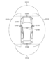
- the microcomputer 12051 can obtain the distance to each solid object within the imaging ranges 12111 to 12114 and the change in this distance over time (relative speed with respect to the vehicle 12100) based on the distance information obtained from the imaging units 12101 to 12104, and can extract as a preceding vehicle, in particular, the closest solid object on the path of the vehicle 12100 that is traveling in approximately the same direction as the vehicle 12100 at a predetermined speed (e.g., 0 km/h or faster). Furthermore, the microcomputer 12051 can set the inter-vehicle distance that should be maintained in advance in front of the preceding vehicle, and perform automatic braking control (including follow-up stop control) and automatic acceleration control (including follow-up start control). In this way, cooperative control can be performed for the purpose of automatic driving, which runs autonomously without relying on the driver's operation.
- automatic braking control including follow-up stop control
- automatic acceleration control including follow-up start control
- the microcomputer 12051 classifies and extracts three-dimensional object data on three-dimensional objects, such as two-wheeled vehicles, ordinary vehicles, large vehicles, pedestrians, utility poles, and other three-dimensional objects, based on the distance information obtained from the imaging units 12101 to 12104, and can use the data to automatically avoid obstacles.
- the microcomputer 12051 distinguishes obstacles around the vehicle 12100 into obstacles that are visible to the driver of the vehicle 12100 and obstacles that are difficult to see.
- At least one of the imaging units 12101 to 12104 may be an infrared camera that detects infrared rays.
- the microcomputer 12051 can recognize a pedestrian by determining whether or not a pedestrian is present in the image captured by the imaging units 12101 to 12104. The recognition of such a pedestrian is performed, for example, by a procedure of extracting feature points in the image captured by the imaging units 12101 to 12104 as infrared cameras, and a procedure of performing pattern matching processing on a series of feature points that indicate the contour of an object to determine whether or not it is a pedestrian.
- the technology disclosed herein can be applied to, for example, the image capture unit 12031. Specifically, it can be applied to the light detection device 1A in FIG. 1.
- the intersecting regions of the pixel separation units include a first region extending in the row direction and a second region extending in the column direction,
- an opening pattern for removing a buried film in the recessed region is formed on both ends of the first region that have the first line width except for the intersection with the second region;
- Each of the plurality of pixels is a photoelectric conversion unit located on a light receiving surface side of the light shielding unit in a thickness direction of the semiconductor layer, the photoelectric conversion unit performing photoelectric conversion on the light incident from the light receiving surface to generate electric charges; a charge retention portion located on an element formation surface side of the light shielding portion in a thickness direction of the semiconductor layer, the charge retention portion retaining charges transferred from the photoelectric conversion portion;
- the light detection device according to (7) above, (9)
- Each of the plurality of pixels includes a vertical gate electrode that reaches the photoelectric conversion unit and a transfer transistor that transfers charges from the photoelectric conversion unit to the charge storage unit;
- each of the plurality of pixels has a charge-shielding portion interposed between the edge of the opening of the light-shielding portion closer to the charge storage portion and the vertical gate electrode, which blocks the transfer of charges to the transfer transistor.
- the film type embedded in the pixel separation portion is a silicon-based film type.
- the film type embedded in the pixel separating portion is a metal-based film type.
- the pixel separating portion has a hard mask opening pattern formed in a recessed region having a line width larger than the first line width.
- a method for manufacturing a photodetector including: a semiconductor layer having a light-receiving surface on which light is incident and an element formation surface located on the opposite side of the light-receiving surface; a plurality of pixels arranged in a matrix in the semiconductor layer and capable of generating an electric signal in response to light incident from the light-receiving surface; and a pixel separation section extending in a depth direction from the light-receiving surface of the semiconductor layer to the element formation surface and separating adjacent pixels, the method comprising the steps of: forming a recessed region having a first depth and a first line width in the pixel separation portion, the recessed region extending in a row direction or a column direction in a plan view; forming a recessed region having a second depth different from the first depth with a second line width different from the first line width so as to match the recessed region of the first depth; forming a buried film in the recessed region; forming a hard mask opening pattern in the recessed region having
Landscapes
- Solid State Image Pick-Up Elements (AREA)
Abstract
トレンチ形状を加工する際に、簡単な工程により加工パターンに依存した深さばらつきを低減し得る光検出装置を提供する。光検出装置は、半導体層と、複数の画素と、画素分離部とを備える。半導体層は、光が入射する受光面及び前記受光面の反対側に位置する素子形成面を有する。複数の画素は、半導体層に行列状に配置され、受光面から入射した光に応じて電気信号を生成する。画素分離部は、半導体層の受光面から素子形成面への深さ方向に延伸し、隣接する前記画素の間を分離する。画素分離部は、平面視において、行方向または列方向へ延伸され、第1の深さを有する掘り込み領域を第1の線幅で形成され、第1の深さと異なる第2の深さを有する掘り込み領域を、第1の深さの掘り込み領域に合わせるように、第1の線幅とは異なる第2の線幅で形成される。
Description
本開示に係る技術(本技術)は、光検出装置、光検出装置の製造方法、及び光検出装置を備える電子機器に関する。
従来、デジタルスチルカメラやデジタルビデオカメラなどの撮像機能を備えた電子機器においては、光検出装置として、例えば、CCD(Charge Coupled Device)やCMOS(Complementary Metal Oxide Semiconductor)イメージセンサなどの固体撮像素子が使用されている。光検出装置は、光電変換を行うフォトダイオード(光電変換素子)とトランジスタとが組み合わされた画素を有しており、平面的に配置された複数の画素から出力される画素信号に基づいて画像が構築される。
ところで、画素に強い光が入射された場合、その画素のフォトダイオードに蓄積されている電荷が飽和してあふれ出し、ブルーミングと呼ばれる現象が発生することがある。このため、画素間を貫通トレンチにより分離し、画素間にまたがってトランジスタ等の素子を配置する箇所に非貫通トレンチを形成する固体撮像装置が提案されている。
ところで、貫通トレンチ及び非貫通トレンチ等の深いトレンチ形状を加工する際、もしくはドライエッチングにて加工する際、加工パターンに依存して加工深さにばらつきが生じる現象、つまりマイクロローディング現象が発生する。このマイクロローディング現象により、遮光性能確保のために、プロセス設計の難易度が増加する。また、貫通トレンチ構造の場合に、マイクロローディング現象により、下層へのブレイクマージンを確保できない。さらに、フォトダイオードとMEM(メモリ)を縦方向に積層する構造においては、マイクロローディング厚に依存して遮光帯幅が大きくなり、画素設計視点において課題が生じる。
下記特許文献1には、複数の画素同士を分離する分離領域を配置するとともに、画素の隅部に非分離領域を形成することにより、マイクロローディング現象を低減する撮像素子が開示されている。つまり、特許文献1に開示されている撮像素子は、光電変換素子間の遮光トレンチ加工において、加工パターンが重なる直交箇所で生じる加工深さばらつきを回避するため、直交箇所を削除する。
ところで、近年では、遮光トレンチ加工において、加工パターンの直交箇所を削除することなく、簡単な工程によりマイクロローディング現象を低減する手法が強く望まれている。
本開示はこのような事情に鑑みてなされたもので、トレンチ形状を加工する際に、簡単な工程により加工パターンに依存した深さばらつきを低減し得る光検出装置、光検出装置の製造方法及び電子機器を提供することを目的とする。
本開示の一態様は、光が入射する受光面及び前記受光面の反対側に位置する素子形成面を有する半導体層と、前記半導体層に行列状に配置され、前記受光面から入射した光に応じて電気信号を生成可能な複数の画素と、前記半導体層の前記受光面から前記素子形成面への深さ方向に延伸し、隣接する前記画素の間を分離する画素分離部と、を備え、前記画素分離部は、平面視において、行方向または列方向へ延伸され、第1の深さを有する掘り込み領域を第1の線幅で形成され、前記第1の深さと異なる第2の深さを有する掘り込み領域を、前記第1の深さの掘り込み領域に合わせるように、前記第1の線幅とは異なる第2の線幅で形成される、光検出装置である。
本開示の他の態様は、光が入射する受光面及び前記受光面の反対側に位置する素子形成面を有する半導体層と、前記半導体層に行列状に配置され、前記受光面から入射した光に応じて電気信号を生成可能な複数の画素と、前記半導体層の前記受光面から前記素子形成面への深さ方向に延伸し、隣接する前記画素の間を分離する画素分離部と、を備える光検出装置の製造方法であって、平面視において、行方向または列方向へ延伸される前記画素分離部の、第1の深さを有する掘り込み領域を第1の線幅で形成することと、前記第1の深さと異なる第2の深さを有する掘り込み領域を、前記第1の深さの掘り込み領域に合わせるように、前記第1の線幅とは異なる第2の線幅で形成することと、前記掘り込み領域内に、埋め込み膜を形成することと、前記掘り込み領域のうち前記第1の線幅より太い線幅の掘り込み領域にハードマスク開口パターンを形成することと、前記ハードマスク開口パターンに基づいて、前記掘り込み領域内の前記埋め込み膜を除去することと、を備える、光検出装置の製造方法である。
さらに、本開示の他の態様は、光が入射する受光面及び前記受光面の反対側に位置する素子形成面を有する半導体層と、前記半導体層に行列状に配置され、前記受光面から入射した光に応じて電気信号を生成可能な複数の画素と、前記半導体層の前記受光面から前記素子形成面への深さ方向に延伸し、隣接する前記画素の間を分離する画素分離部と、を備え、前記画素分離部は、平面視において、行方向または列方向へ延伸され、第1の深さを有する掘り込み領域を第1の線幅で形成され、前記第1の深さと異なる第2の深さを有する掘り込み領域を、前記第1の深さの掘り込み領域に合わせるように、前記第1の線幅とは異なる第2の線幅で形成される、光検出装置を備えた、電子機器である。
以下において、図面を参照して本開示の実施形態を説明する。以下の説明で参照する図面の記載において、同一又は類似の部分には同一又は類似の符号を付し、重複する説明を省略する。但し、図面は模式的なものであり、厚みと平面寸法との関係、各装置や各部材の厚みの比率等は現実のものと異なることに留意すべきである。したがって、具体的な厚みや寸法は以下の説明を参酌して判定すべきものである。また、図面相互間においても互いの寸法の関係や比率が異なる部分が含まれていることは勿論である。
本明細書において、「第1導電型」はp型又はn型の一方であり、「第2導電型」はp型又はn型のうちの「第1導電型」とは異なる一方を意味する。また、「n」や「p」に付す「+」や「-」は、「+」及び「-」が付記されていない半導体領域に比して、それぞれ相対的に不純物密度が高い又は低い半導体領域であることを意味する。但し、同じ「n」と「n」とが付された半導体領域であっても、それぞれの半導体領域の不純物密度が厳密に同じであることを意味するものではない。
また、以下の説明における上下等の方向の定義は、単に説明の便宜上の定義であって、本開示の技術的思想を限定するものではない。例えば、対象を90°回転して観察すれば上下は左右に変換して読まれ、180°回転して観察すれば上下は反転して読まれることは勿論である。
なお、本明細書中に記載される効果はあくまで例示であって限定されるものでは無く、また他の効果があってもよい。
なお、本明細書中に記載される効果はあくまで例示であって限定されるものでは無く、また他の効果があってもよい。
<第1の実施形態>
本開示の第1の実施形態では、光検出装置として、裏面照射型のCMOS(Complementary Metal Oxide Semiconductor)イメージセンサである固体撮像装置に本技術を適用した一例について説明する。
本開示の第1の実施形態では、光検出装置として、裏面照射型のCMOS(Complementary Metal Oxide Semiconductor)イメージセンサである固体撮像装置に本技術を適用した一例について説明する。
(光検出装置の全体構成)
まず、光検出装置1Aの全体構成について説明する。
図1に示すように、本開示の第1実施形態に係る光検出装置1Aは、平面視したときの二次元平面形状が方形状の半導体チップ2を主体に構成されている。即ち、光検出装置1Aは、半導体チップ2に搭載されている。
まず、光検出装置1Aの全体構成について説明する。
図1に示すように、本開示の第1実施形態に係る光検出装置1Aは、平面視したときの二次元平面形状が方形状の半導体チップ2を主体に構成されている。即ち、光検出装置1Aは、半導体チップ2に搭載されている。
図1に示すように、光検出装置1Aが搭載された半導体チップ2は、互いに直交するX方向及びY方向を含む二次元平面において、中央部に設けられた方形状の画素アレイ部2Aと、この画素アレイ部2Aの外側に画素アレイ部2Aを囲むようにして設けられた周辺部2Bとを備えている。
画素アレイ部2Aは、集光される光を受光する受光面である。そして、画素アレイ部2Aには、X方向及びY方向を含む二次元平面において複数の画素3が行列状に配置されている。換言すれば、画素3は、二次元平面内で互いに直交するX方向及びY方向のそれぞれの方向に繰り返し配置されている。
図1に示すように、周辺部2Bには、複数のボンディングパッド14が配置されている。複数のボンディングパッド14の各々は、例えば、半導体チップ2の二次元平面における4つの辺の各々の辺に沿って配列されている。複数のボンディングパッド14の各々は、半導体チップ2を外部装置と電気的に接続する際に用いられる入出力端子である。
半導体チップ2は、図2に示すロジック回路13を備えている。ロジック回路13は、図2に示すように、垂直駆動回路4、カラム信号処理回路5、水平駆動回路6、出力回路7及び制御回路8などを含む。ロジック回路13は、電界効果トランジスタとして、例えば、nチャネル導電型のMOSFET(Metal Oxide Semiconductor Field Effect Transistor)及びpチャネル導電型のMOSFETを有するCMOS(Complenentary MOS)回路で構成されている。
垂直駆動回路4は、例えばシフトレジスタによって構成されている。垂直駆動回路4は、所望の画素駆動線10を順次選択し、選択した画素駆動線10に画素3を駆動するためのパルスを供給し、各画素3を行単位で駆動する。即ち、垂直駆動回路4は、画素アレイ部2Aの各画素3を行単位で順次垂直方向に選択走査し、各画素3の光電変換素子が受光量に応じて生成した信号電荷に基づく画素3からの画素信号を、垂直信号線11を通してカラム信号処理回路5に供給する。
カラム信号処理回路5は、例えば画素3の列毎に配置されており、1行分の画素3から出力される信号に対して画素列毎にノイズ除去等の信号処理を行う。例えばカラム信号処理回路5は、画素固有の固定パターンノイズを除去するためのCDS(Correlated Double Sampling:相関2重サンプリング)及びAD(Analog Digital)変換等の信号処理を行う。
水平駆動回路6は、例えばシフトレジスタによって構成されている。水平駆動回路6は、水平走査パルスをカラム信号処理回路5に順次出力することによって、カラム信号処理回路5の各々を順番に選択し、カラム信号処理回路5の各々から信号処理が行われた画素信号を水平信号線12に出力させる。
出力回路7は、カラム信号処理回路5の各々から水平信号線12を通して順次に供給される画素信号に対し、信号処理を行って出力する。信号処理としては、例えば、バッファリング、黒レベル調整、列ばらつき補正、各種デジタル信号処理等を用いることができる。
制御回路8は、垂直同期信号、水平同期信号、及びマスタクロック信号に基づいて、垂直駆動回路4、カラム信号処理回路5、及び水平駆動回路6等の動作の基準となるクロック信号や制御信号を生成する。そして、制御回路8は、生成したクロック信号や制御信号を、垂直駆動回路4、カラム信号処理回路5、及び水平駆動回路6等に出力する。
複数の画素3の各々の画素3は、図3に示す光電変換領域27と、図示していないが複数の画素トランジスタとを含む。複数の画素トランジスタとしては、例えば、転送トランジスタ、リセットトランジスタ、選択トランジスタ、増幅トランジスタの4つのトランジスタを採用できる。また、複数の画素トランジスタとしては、例えば選択トランジスタを除いた3つのトランジスタを採用してもよい。
<光検出装置の具体的な構成>
次に、光検出装置1Aの具体的な構成について説明する。
図3に示すように、半導体チップ2は、複数の光電変換領域27が設けられた半導体層20と、この半導体層20の厚さ方向(Z方向)において互いに反対側に位置する第1の面S1及び第2の面S2のうちの第2の面S2側である光入射面側に配置されたカラーフィルタ層40とを備えている。
また、半導体チップ2は、カラーフィルタ層40の光入射面側(半導体層20側とは反対側)に配置された複数のマイクロレンズ45(オンチップレンズ、ウエハレンズ)を更に備えている。
また、半導体チップ2は、半導体層20の第1の面S1側に配置された多層配線層30と、この多層配線層30の半導体層20側とは反対側に配置された支持基板34とを更に備えている。
次に、光検出装置1Aの具体的な構成について説明する。
図3に示すように、半導体チップ2は、複数の光電変換領域27が設けられた半導体層20と、この半導体層20の厚さ方向(Z方向)において互いに反対側に位置する第1の面S1及び第2の面S2のうちの第2の面S2側である光入射面側に配置されたカラーフィルタ層40とを備えている。
また、半導体チップ2は、カラーフィルタ層40の光入射面側(半導体層20側とは反対側)に配置された複数のマイクロレンズ45(オンチップレンズ、ウエハレンズ)を更に備えている。
また、半導体チップ2は、半導体層20の第1の面S1側に配置された多層配線層30と、この多層配線層30の半導体層20側とは反対側に配置された支持基板34とを更に備えている。
半導体層20は、例えば単結晶シリコンからなるp型の半導体基板で構成されている。複数の光電変換領域27の各々の光電変換領域27は、画素アレイ部2Aにおいて、複数の画素3の各々の画素3に対応して行列状に配置されている。そして、各光電変換領域27は、半導体層20に設けられた分離領域24(画素分離部の一例)によって区画されている。分離領域24は、半導体層20の第2の面S2側から第1の面S1側に向かって延伸し、平面視で互に隣り合う光電変換領域27間を電気的及び光学的に分離している。分離領域24は、半導体層20の第2の面S2側から第1の面S1側に向かって延伸するトレンチ22(掘り込み領域の一例)と、このトレンチ22内に埋め込まれた絶縁膜23(埋め込み膜の一例)とを含む。絶縁膜23としては、例えば酸化シリコン膜を用いることができる。この第1実施形態の分離領域24は、これに限定されないが、半導体層20の第2の面S2及び第1の面S1に亘って延伸している。
ここで、半導体層20の第1の面S1を素子形成面又は主面、第2の面S2側を光入射面(受光面の一例)又は裏面と呼ぶこともある。この第1実施形態の光検出装置1Aは、半導体層20の第2の面(光入射面,裏面)S2側から入射した光を、半導体層20に設けられた光電変換領域27で光電変換する。
また、平面視とは、半導体層20の厚さ方向(Z方向)に沿う方向から見た場合を指す。また、断面視とは、半導体層20の厚さ方向(Z方向)に沿う断面を半導体層20の厚さ方向(Z方向)と直交する方向(X方向又はY方向)から見た場合を指す。
また、平面視とは、半導体層20の厚さ方向(Z方向)に沿う方向から見た場合を指す。また、断面視とは、半導体層20の厚さ方向(Z方向)に沿う断面を半導体層20の厚さ方向(Z方向)と直交する方向(X方向又はY方向)から見た場合を指す。
なお、分離領域24としては、トレンチ22内において、金属膜の両側を絶縁膜で挟んだサンドイッチ構造を採用することもできる。
図3に示すように、複数の光電変換領域27の各々の光電変換領域27には、例えばp型の半導体領域からなるp型のウエル領域21と、n型の半導体領域21aとが構成されている。また、複数の光電変換領域27の各々の光電変換領域27には、詳細に図示していないが、光電変換素子として例えばフォトダイオード(PD:Photo Diode)素子が構成され、更に転送トランジスタが構成されている。即ち、画素アレイ部2Aには、半導体層20に埋設された光電変換素子及び転送トランジスタを含む画素3が行列状(二次元マトリクス状)に複数配置されている。光電変換領域27では、入射光の光量に応じた信号電荷が生成され、生成された信号電荷が蓄積される。n型の半導体領域21aはp型のウエル領域21内に設けられている。フォトダイオードPDは、p型のウエル領域21及びn型の半導体領域21aを含む。
図3に示すように、多層配線層30は、半導体層20の光入射面(第2の面S2)側とは反対側の第1の面S1側に配置されており、配線32を含む配線層が層間絶縁膜31を介して複数段積層された構成になっている。各配線層の配線32を介して各画素3を構成する画素トランジスタが駆動される。多層配線層30は、半導体層20の光入射面側(第2の面S2側)とは反対側に配置されているので、配線32のレイアウトを自由に設定することができる。
カラーフィルタ層40は、これに限定されないが、例えば、赤色(R)の第1カラーフィルタ部41と、緑色(G)の第2カラーフィルタ部42と、青色(B)の第3カラーフィルタ部43とを含む。この第1~第3カラーフィルタ部41~43は、画素アレイ部2Aにおいて、複数の画素3の各々の画素3、即ち、複数の光電変換領域27の各々の光電変換領域27に対応して行列状に配置されている。第1~第3カラーフィルタ部41~43は、光電変換領域27に受光させたい入射光の特定の波長を透過し、透過させた入射光を光電変換領域27に入射させる構成になっている。
複数のマイクロレンズ45の各々のマイクロレンズ45は、画素アレイ部2Aにおいて、複数の画素3の各々の画素3、即ち複数の光電変換領域27の各々の光電変換領域27に対応して行列状に配置されている。マイクロレンズ45は、照射光を集光し、集光した光を、カラーフィルタ層40を介して半導体層20の光電変換領域27に効率よく入射させる。複数のマイクロレンズ45は、カラーフィルタ層40の光入射面側においてマイクロレンズアレイを構成している。
支持基板34は、多層配線層30の半導体層20に面する側とは反対側の面に設けられている。支持基板34は、光検出装置1Aの製造段階において、半導体層20の強度を確保するための基板である。支持基板34の材料としては、例えば、シリコン(Si)を用いることができる。
図3に示すように、半導体層20とカラーフィルタ層40との間には、半導体層20側から平坦化膜36及び接着膜38がこの順で積層されている。
平坦化膜36は、半導体層20の光入射面側が凹凸のない平坦面となるように、画素アレイ部2Aにおいて、半導体層20の光入射面側全体を覆っている。平坦化膜36としては、例えば酸化シリコン(SiO2)膜を用いることができる。
接着膜38は、平坦化膜36と、カラーフィルタ層40との間に配置される。接着膜38としては、例えば酸化シリコン膜が用いられている。
以上の構成を有する光検出装置1Aでは、光が半導体チップ2のマイクロレンズ45側から照射され、照射された光がマイクロレンズ45及びカラーフィルタ部41,42,43を個別に透過し、透過した光が光電変換領域27で光電変換されることで、信号電荷が生成される。そして、生成された信号電荷が、半導体層20の第1の面S1側に形成された画素トランジスタを介して、多層配線層30の配線32からなる垂直信号線11によって画素信号として出力される。また、光電変換領域27で生成された信号電荷間の差に基づき、被写体までの間の距離が算出される。
<分離領域及び光電変換領域>
次に、分離領域24及び光電変換領域27の具体的な構成について説明する。
次に、分離領域24及び光電変換領域27の具体的な構成について説明する。
図4に示すように、分離領域24は、平面視で線幅a1でX方向に延伸する第1部分24xと、Y方向に延伸する第2部分24yと、を含む。第1部分24xと第2部分24yとは、各々の延伸方向が直交している。複数の光電変換領域27の各々の光電変換領域27は、X方向の両端側が分離領域24の2つの第2部分24yで区画され、Y方向の両端側が分離領域24の2つの第1部分24xで区画されている。分離領域24に含まれる第1部分24x及び第2部分24yの各々は、半導体層20第2の面及び第1の面に亘って延伸している。そして、第1部分24x及び第2部分24yの各々は、半導体層20の第2の面S2及び第1の面S1に亘って延伸するトレンチ22と、このトレンチ22内に埋め込まれた絶縁膜23とを含む。
<第1の実施形態の比較例>
図5Aは、第1の実施形態の比較例における分離領域24の直進パターンの平面図である。図5Bは、図5Aの一点鎖線で示す分離領域24の直進パターンの断面図である。分離領域24の第1部分24xにおいて、直進パターンの両端は、マイクロローディング現象によって直進パターンの真ん中の深さb1に比べてt1ほど浅い深さb2となる。このため、分離領域24が非貫通となることにより、光が漏れ込み、遮光性が悪くなる。
図5Aは、第1の実施形態の比較例における分離領域24の直進パターンの平面図である。図5Bは、図5Aの一点鎖線で示す分離領域24の直進パターンの断面図である。分離領域24の第1部分24xにおいて、直進パターンの両端は、マイクロローディング現象によって直進パターンの真ん中の深さb1に比べてt1ほど浅い深さb2となる。このため、分離領域24が非貫通となることにより、光が漏れ込み、遮光性が悪くなる。
図6Aは、第1の実施形態の比較例における分離領域24の交差パターンの平面図である。図6Bは、図6Aの一点鎖線で示す分離領域24の交差パターンの断面図である。分離領域24の第1部分24xと第2部分24yとの交差する箇所(以後、交差箇所25と称する)の深さb3は、マイクロローディング現象によって交差しない箇所の深さb1に比べてt2ほど深くなる。このため、分離領域24が下層を壊す恐れがあり、多層配線層30の金属を露出させる恐れがある。
<第1の実施形態による解決手段>
図7は、本開示の第1の実施形態における分離領域24の交差パターンの平面図である。図8は、本開示の第1の実施形態における分離領域24の直進パターンの平面図である。
図7は、本開示の第1の実施形態における分離領域24の交差パターンの平面図である。図8は、本開示の第1の実施形態における分離領域24の直進パターンの平面図である。
本開示の第1の実施形態では、図7に示すように、分離領域24の第1部分24xと第2部分24yとの交差箇所25の線幅a3を、交差しない箇所の線幅a1より細く形成して、交差箇所25の深さb3を交差しない箇所の深さb1に合わせ込むようにしている。つまり、マイクロローディング現象の発生箇所の面積は、分離領域24の加工箇所の面積に相当する。また、本開示の第1の実施形態では、交差パターンの両端の線幅a2を線幅a1より太く形成している。なお、線幅a1より細くする範囲及び太くする範囲は、分離領域24のトレンチ22に酸化シリコン(SiO2)等の絶縁膜23を埋め込み可能な範囲である。
また、本開示の第1の実施形態では、図8に示すように、分離領域24の直進パターンの両端の線幅a2を、線幅a1より太く形成して、両端の深さb2を深さb1に合わせ込むようにしている。
本開示の第1の実施形態において、第2の面S2側から分離領域24を形成する場合に、光電変換領域27を貫通するトレンチを形成する必要があるが、PMD(Pre-Metal Directric Layer)を貫通すると多層配線層30の金属が露出するため、コンタミネーション汚染の懸念があり、図9に示すように、ストッパー層50を形成しておく必要がある。ストッパー層50として、第1の酸化シリコン膜51と、窒化シリコン膜52と、第2の酸化シリコン膜53等の異種膜を形成しておく必要がある。ストッパー層50は、光漏れ込みパスとなりうるが、マイクロローディング現象を抑制することで、ストッパー層50の膜厚を最小限にすることができ、例えばMEM(電荷保持部の一例)への光漏れ込みを最小化することができる。
(アクティブパターン形成方法)
図10A乃至図10Cは、トレンチパターンからアクティブパターンの形成工程を示す平面図である。
分離領域24の形成工程は、裏面照射型イメージセンサ―の裏面化後の工程位置だけではなく、トランジスタ等を形成するFEOL(Front End Of Line)工程でも形成可能である。
図10A乃至図10Cは、トレンチパターンからアクティブパターンの形成工程を示す平面図である。
分離領域24の形成工程は、裏面照射型イメージセンサ―の裏面化後の工程位置だけではなく、トランジスタ等を形成するFEOL(Front End Of Line)工程でも形成可能である。
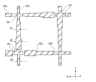
FEOL工程にてトレンチ22を形成する場合、このトレンチパターンがアクティブパターンに転用されることもある。図10Aにおいて、分離領域24の第1部分24xと第2部分24yとの間に、非分離領域26が形成されている箇所が含まれる。分離領域24の交差箇所25では、分離領域24はマイクロローディング現象によって深くなる。また、非分離領域26では、分離領域24の第1部分24xの端、及び第1部分24xの端は、マイクロローディング現象によって浅くなる。
そこで、図10Bに示すように、分離領域24の交差箇所25では、第1部分24x及び第2部分24yそれぞれの線幅a1を線幅a3に細めて形成する。また、非分離領域26では、第1部分24x及び第2部分24yそれぞれの端の線幅a1を線幅a2に太くして形成する。ところで、線幅a1と線幅a2との境目の凸部551、及び線幅a1と線幅a3との境目の凸部552では、応力集中、電界集中による特性劣化が懸念される。
そこで、図10Cに示すように、分離領域24のトレンチ22を一度平坦化し、トレンチ22の上にアクティブパターン54を重ねて形成する。アクティブパターン54は、分離領域24の線幅a2の領域に後述するハードマスク開口パターンを配置して形成される。また、アクティブパターン54で囲まれる画素3内には、素子分離部(STI)56が形成される。これにより、特性劣化は回避可能である。
(光検出装置の製造方法)
図11A乃至図11Eは、本開示の第1の実施形態における光検出装置1Aの分離領域24及び素子分離部56の形成方法の工程手順を示す断面図である。なお、光検出装置1Aは、成膜装置(CVD(Chemical Vapor Deposition)装置、スパッタ装置を含む)、イオン注入装置、熱処理装置、エッチング装置、CMP(Chemical Mechanical Polishing)装置、貼り合わせ装置など、各種の装置を用いて製造される。以下、これらの装置を、製造装置と総称する。
図11A乃至図11Eは、本開示の第1の実施形態における光検出装置1Aの分離領域24及び素子分離部56の形成方法の工程手順を示す断面図である。なお、光検出装置1Aは、成膜装置(CVD(Chemical Vapor Deposition)装置、スパッタ装置を含む)、イオン注入装置、熱処理装置、エッチング装置、CMP(Chemical Mechanical Polishing)装置、貼り合わせ装置など、各種の装置を用いて製造される。以下、これらの装置を、製造装置と総称する。
図11Aにおいて、半導体チップ2を用意し、製造装置は、半導体チップ2の半導体層20の第2の面S2(光入射面)に例えば酸化シリコン(SiO2)等の絶縁膜61を積層し、絶縁膜61の上面に平坦化膜36を積層し、第2の面S2からトレンチ22を貫通して形成する。そして、製造装置は、トレンチ22に例えばPoly-Siから成る絶縁膜23を埋め込む。絶縁膜23は、平坦化膜36の上面を覆っている。
次に、図11Bにおいて、製造装置は、エッチバック工程にて平坦化膜36の上面を覆う絶縁膜23を除去する。続いて、図11Cにおいて、製造装置は、トレンチ22内の絶縁膜23が除去された箇所に例えば塗布膜62を積層する。塗布膜62は、塗布プロセス等による流動性のある成膜材料である。
次に、図11Dにおいて、製造装置は、平坦化膜36の上面及び塗布膜62の上面に反射防止膜63を形成し、リソグラフィ工程にて反射防止膜63上にレジスト64にパターニングする。ここでは、分離領域24の線幅a2の領域にレジスト64を形成してハードマスク開口パターンを配置する。
次に、図11Eにおいて、製造装置は、ドライエッチング工程にて反射防止膜63及びレジスト64を除去し、アクティブパターン54を形成し、素子分離部56を形成する。
<第1の実施形態による作用効果>
以上のように第1の実施形態によれば、分離領域24において、トレンチ22が浅くなる箇所に関しては線幅を太くし、トレンチ22が深くなる箇所に関しては線幅を細くすることで、マイクロローディング現象のコントロールが可能となる。このため、マイクロローディング現象の影響を緩和することで、画素3、光電変換領域27の構造のポテンシャル設計の自由度が得られ、特性の向上が可能となる。
以上のように第1の実施形態によれば、分離領域24において、トレンチ22が浅くなる箇所に関しては線幅を太くし、トレンチ22が深くなる箇所に関しては線幅を細くすることで、マイクロローディング現象のコントロールが可能となる。このため、マイクロローディング現象の影響を緩和することで、画素3、光電変換領域27の構造のポテンシャル設計の自由度が得られ、特性の向上が可能となる。
また、第1の実施形態によれば、マイクロローディング現象を低減するために、分離領域24の線幅を変えると、アクティブエリアの凸部551,552への応力が集中し、また電界集中による特性劣化が懸念されることになるため、分離領域24を一度平坦化し、分離領域24の太い線幅の領域にハードマスク開口パターンを配置してアクティブパターン54を分離領域24に重ねて形成することで、特性劣化は回避可能である。
<第1の実施形態の第1の変形例>
本開示の第1の実施形態の第1の変形例は、FEOL工程において、裏面化後にトレンチ22の中の絶縁膜23を除去し、メタル膜を埋め戻すことに関する。FEOL工程では、高い遮光性が期待できるメタル膜はコンタミネーション汚染の視点において使用できず、酸化シリコンSiO2やPoly-Si等の絶縁膜23を埋め込むこととなる。そのため、FEOL工程にて分離領域24を形成した場合、メタル膜を分離領域24のトレンチ22中に埋め込むためには、裏面化後にトレンチ22中の絶縁膜23を除去し、メタル膜を埋め戻す作業が必要となる。
本開示の第1の実施形態の第1の変形例は、FEOL工程において、裏面化後にトレンチ22の中の絶縁膜23を除去し、メタル膜を埋め戻すことに関する。FEOL工程では、高い遮光性が期待できるメタル膜はコンタミネーション汚染の視点において使用できず、酸化シリコンSiO2やPoly-Si等の絶縁膜23を埋め込むこととなる。そのため、FEOL工程にて分離領域24を形成した場合、メタル膜を分離領域24のトレンチ22中に埋め込むためには、裏面化後にトレンチ22中の絶縁膜23を除去し、メタル膜を埋め戻す作業が必要となる。
(光検出装置の製造方法)
図12A乃至図12Dは、本開示の第1の実施形態の第1の変形例における光検出装置1Aの分離領域24の絶縁膜23をメタル膜に埋め戻す方法の工程手順を示す断面図である。
図12A乃至図12Dは、本開示の第1の実施形態の第1の変形例における光検出装置1Aの分離領域24の絶縁膜23をメタル膜に埋め戻す方法の工程手順を示す断面図である。
図12Aにおいて、製造装置は、トレンチ22に例えばPoly-Siから成る絶縁膜23を埋め込んだ半導体層20の第2の面S2に酸化シリコン(SiO2)等のレジスト71をハードマスクとして成膜する。続いて、図12Bにおいて、製造装置は、リソグラフィ工程にてトレンチ22上にホール形状等のパターニングを行い、ホール72を形成する。
次に、図12Cにおいて、製造装置は、ウェットエッチング工程にてトレンチ22に埋め込まれた絶縁膜23を除去する。そして、図12Dにおいて、製造装置は、レジスト71を除去する。
上記ホール72は、絶縁膜23のエッチングパターンの合わせズレを考慮して、分離領域24の第1部分24xと第2部分24yとの交差箇所25に配置される。しかし、交差箇所25を細線化することで合わせマージンが悪化する。そこで、本開示の第1の実施形態の第1の変形例では、図13に示すように、分離領域24の第1部分24xの線幅a1となる領域24x1,24x2にホール72を配置する。また、分離領域24の第2部分24yの線幅a1となる領域24y1,24y2にホール72を配置する。これにより、デザイン制約が緩和される。
<第1の実施形態の第2の変形例>
本開示の第1の実施形態の第2の変形例は、図14に示すように、分離領域24の交差箇所25のコーナー部がリソグラフィ起因によって開口面積が大きくなることでマイクロローディングが悪化してしまうことへの対策である。
本開示の第1の実施形態の第2の変形例は、図14に示すように、分離領域24の交差箇所25のコーナー部がリソグラフィ起因によって開口面積が大きくなることでマイクロローディングが悪化してしまうことへの対策である。
(光検出装置の製造方法)
図15A乃至図15Cは、本開示の第1の実施形態の第2の変形例における光検出装置1Aの分離領域24の交差箇所25を形成する方法の工程手順を示す平面図及び断面図である。図15A乃至図15Cの(1)は平面図であり、図15A乃至図15Cの(2)は(1)の一点鎖線で示す分離領域24の断面図である。
図15A乃至図15Cは、本開示の第1の実施形態の第2の変形例における光検出装置1Aの分離領域24の交差箇所25を形成する方法の工程手順を示す平面図及び断面図である。図15A乃至図15Cの(1)は平面図であり、図15A乃至図15Cの(2)は(1)の一点鎖線で示す分離領域24の断面図である。
図15Aにおいて、製造装置は、リソグラフィ工程にて分離領域24の第1部分24xを形成するために、半導体層20の第2の面S2にレジスト81をハードマスクとして成膜する。そして、製造装置は、分離領域24の第1部分24xの図15A中矢印Xで示す方向に沿って開口部82を形成する。
次に、図15Bにおいて、製造装置は、リソグラフィ工程にて分離領域24の第2部分24yを形成するために、半導体層20の第2の面S2にレジスト83をハードマスクとして成膜する。そして、製造装置は、分離領域24の第2部分24yの図15B中矢印Yで示す方向に沿って開口部84を形成する。
次に、図15Cにおいて、製造装置は、ウェットエッチング工程等にて開口部82,83に沿って半導体層20のシリコンを除去して、トレンチ22を形成する。
<第1の実施形態の第2の変形例による作用効果>
第1の実施形態の第2の変形例によれば、分離領域24の交差箇所25がリソグラフィ起因によって開口面積が大きくなることでマイクロローディングが悪化してしまうため、分離領域24の第1部分24xと、第2部分24yとを別々に加工することで、交差箇所25の矩形性を上げることができる。
第1の実施形態の第2の変形例によれば、分離領域24の交差箇所25がリソグラフィ起因によって開口面積が大きくなることでマイクロローディングが悪化してしまうため、分離領域24の第1部分24xと、第2部分24yとを別々に加工することで、交差箇所25の矩形性を上げることができる。
<第2の実施形態>
本開示の第2の実施形態に係る光検出装置1Bについて説明する。光検出装置1Bは、例えば、CMOS(Complementary Metal Oxide Semiconductor)イメージセンサ等からなるグローバルシャッタ方式の裏面照射型のイメージセンサである。
本開示の第2の実施形態に係る光検出装置1Bについて説明する。光検出装置1Bは、例えば、CMOS(Complementary Metal Oxide Semiconductor)イメージセンサ等からなるグローバルシャッタ方式の裏面照射型のイメージセンサである。
(光検出装置の構成)
図16は、本開示の第2の実施形態に係る光検出装置1Bの一例を示す部分断面図である。
図16は、本開示の第2の実施形態に係る光検出装置1Bの一例を示す部分断面図である。
第1基板30-1は、半導体基板31-1(半導体層の一例)上に絶縁層32-1を積層して構成されている。つまり、絶縁層32-1は、半導体基板31-1の上面に接して形成されている。半導体基板31-1の上面には、第1転送トランジスタTRX、第2転送トランジスタTRM、電荷保持部MEM、第3転送トランジスタTRG、フローティングディフュージョンFDおよび排出トランジスタOFGが形成されている。半導体基板31-1の上面近傍には、電荷保持部MEMが形成されている。従って、半導体基板31-1の上面は、第1転送トランジスタTRXなどの形成面31B-1となっている。
絶縁層32-1内には、第1転送トランジスタTRX、第2転送トランジスタTRM、第3転送トランジスタTRGおよび排出トランジスタOFGのゲート電極や、これらのゲート電極に接続された配線などが設けられている。第1転送トランジスタTRX、第2転送トランジスタTRM、第3転送トランジスタTRGおよび排出トランジスタOFGのゲート電極や、これらのゲート電極に接続された配線は、例えば、金属材料によって形成されている。第1転送トランジスタTRXのゲート電極(垂直ゲート電極VG)は、ポリシリコンによって形成されていてもよい。
半導体基板31-1,41-1は、例えば、シリコン基板で構成されている。半導体基板31-1は、例えば、シリコン(111)基板で構成されている。シリコン(111)基板とは、(111)の結晶方位を有する単結晶シリコン基板である。半導体基板31-1は、上面(形成面31B-1(素子形成面の一例))の一部およびその近傍に、N型半導体領域32B-1を有しており、N型半導体領域32B-1よりも深い領域にN型半導体領域32A-1を有している。半導体基板31-1は、さらに、フローティングディフュージョンFDおよび電荷保持部MEMを有している。第1転送トランジスタTRXのゲート電極(垂直ゲート電極VG)は、半導体基板31-1の上面(形成面31B-1)から、半導体基板31-1の厚さ方向(法線方向)に延在して形成されている。第1転送トランジスタTRXのゲート電極(垂直ゲート電極VG)は、形成面31B-1から、N型半導体領域32A(フォトダイオードPD)に達する深さまで延在している。第1転送トランジスタTRXのゲート電極(垂直ゲート電極VG)は、例えば、半導体基板31-1の厚さ方向(法線方向)に延在する棒状の形状となっている。
第1基板30-1は、例えば、さらに、半導体基板31-1の裏面(受光面31A-1)に接する固定電荷膜38-1を有している。固定電荷膜38-1は、半導体基板31-1の受光面31A-1側の界面準位に起因する暗電流の発生を抑制するため、負の固定電荷を有している。固定電荷膜38-1は、例えば、負の固定電荷を有する絶縁膜によって形成されている。そのような絶縁膜の材料としては、例えば、酸化ハフニウム、酸化ジルコン、酸化アルミニウム、酸化チタンまたは酸化タンタルが挙げられる。固定電荷膜38-1が誘起する電界により、半導体基板31-1の受光面31A-1側の界面にホール蓄積層が形成される。このホール蓄積層によって、界面からの電子の発生が抑制される。第1基板30-1は、例えば、さらに、カラーフィルタ39-1を有している。カラーフィルタ39-1は、半導体基板31-1の受光面31A-1側に設けられている。カラーフィルタ39-1は、例えば、固定電荷膜38-1に接して設けられており、固定電荷膜38-1を介して画素11-1と対向する位置に設けられている。
各画素11-1は、半導体基板31-1の裏面(受光面31A-1)側に受光レンズ50-1を有している。つまり、光検出装置1Bは、画素11-1ごとに1つずつ設けられた複数の受光レンズ50-1を備えている。複数の受光レンズ50-1は、フォトダイオードPDごとに1つずつ設けられており、フォトダイオードPDと対向する位置に配置されている。つまり、光検出装置1Bは、裏面照射型の撮像装置である。受光レンズ50-1は、例えば、カラーフィルタ39-1に接して設けられており、カラーフィルタ39-1および固定電荷膜38-1を介して画素11-1と対向する位置に設けられている。
第1基板30-1は、互いに隣接する2つの画素11-1を電気的かつ光学的に分離する素子分離部34-1,36-1を有している。素子分離部34-1,36-1は、半導体基板31-1の法線方向(厚さ方向)に延在して形成されている。素子分離部34-1,36-1は、半導体基板31-1内において、半導体基板31-1の法線方向(厚さ方向)に積層されている。つまり、素子分離部34-1,36-1は、互いに連結されている。素子分離部34-1,36-1からなる構造体は、受光面31A-1から形成面31B-1まで延在して形成されている。つまり、素子分離部34-1,36-1からなる構造体は、半導体基板31-1および半導体層33-1を貫通している。
素子分離部34-1は、画素11-1(特にフォトダイオードPD)を水平面内方向において取り囲むように形成されており、さらに、半導体基板31-1の法線方向(厚さ方向)に延在して形成されている。素子分離部34-1は、互いに隣接する2つのフォトダイオードPDの間に形成されている。素子分離部34-1は、例えば、金属埋め込み部34A-1およびP型半導体部34B-1によって構成されている。
金属埋め込み部34A-1およびP型半導体部34B-1は、ともに、画素11-1(特にフォトダイオードPD)を水平面内方向において取り囲むとともに、半導体基板31-1の法線方向(厚さ方向)に延在している。P型半導体部34B-1は、金属埋め込み部34A-1の側面に接して形成されており、金属埋め込み部34A-1とフォトダイオードPDとの間に形成されている。金属埋め込み部34A-1は、例えば、CVD(Chemical Vapor Deposition)を用いて形成されている。金属埋め込み部34A-1は、例えば、アルミニウムまたはアルミニウム合金によって形成されている。P型半導体部34B-1は、導電型がP型の半導体によって形成されている。
素子分離部36-1は、画素11-1(特に、第1転送トランジスタTRX、第2転送トランジスタTRM、電荷保持部MEM、第3転送トランジスタTRG、フローティングディフュージョンFDおよび排出トランジスタOFG)を水平面内方向において取り囲むように形成されており、さらに、半導体基板31-1の法線方向(厚さ方向)に延在して形成されている。素子分離部36-1は、半導体基板31-1の法線方向(厚さ方向)において素子分離部34-1と対向する位置に設けられている。素子分離部36-1は、例えば、金属埋め込み部36Aおよび絶縁膜36Bによって構成されている。
金属埋め込み部36A-1および絶縁膜36B-1は、ともに、画素11-1(特に、第1転送トランジスタTRX、第2転送トランジスタTRM、電荷保持部MEM、第3転送トランジスタTRG、フローティングディフュージョンFDおよび排出トランジスタOFG)を水平面内方向において取り囲むとともに、半導体基板31-1の法線方向(厚さ方向)に延在している。絶縁膜36B-1は、金属埋め込み部36A-1の側面に接して形成されており、金属埋め込み部36A-1と画素11-1との間に形成されている。金属埋め込み部36A-1は、例えば、CVDを用いて形成されている。金属埋め込み部36Aは、例えば、アルミニウムまたはアルミニウム合金によって形成されている。絶縁膜36B-1は、例えば、半導体基板31-1を熱酸化することにより形成された酸化膜であり、例えば、酸化シリコンによって形成されている。
素子分離部34-1の上部と素子分離部36-1の下部とが半導体基板31-1の法線方向(厚さ方向)において互いに連結されている。素子分離部34-1および素子分離部36-1からなる複合体が、本開示の「分離部」の一具体例に相当する。素子分離部34-1および素子分離部36-1からなる複合体は、各画素11-1を電気的かつ光学的に分離する。素子分離部34-1および素子分離部36-1からなる複合体は、受光面31A-1から形成面31B-1まで延在して形成されている。つまり、素子分離部34-1および素子分離部36-1からなる複合体は、半導体基板31-1を貫通している。
第1基板30-1は、さらに、フォトダイオードPDと電荷保持部MEMとの間の層内に延在して形成された遮光部37-1を有している。遮光部37-1は、受光面31A-1を介して入射した光の、電荷保持部MEMへの入射を遮る。遮光部37-1は、例えば、金属埋め込み部37A-1および絶縁膜37B-1によって構成されている。絶縁膜37B-1は、金属埋め込み部37A-1の上面、下面および側面に接して形成されており、金属埋め込み部37A-1を覆うように形成されている。
金属埋め込み部37A-1は、例えば、CVDを用いて形成されている。金属埋め込み部37A-1は、例えば、アルミニウムまたはアルミニウム合金によって形成されている。絶縁膜37B-1は、例えば、半導体基板31-1を熱酸化することにより形成された酸化膜であり、例えば、酸化シリコンによって形成されている。絶縁膜37B-1は、SiO2膜(シリコン酸化膜)を含む多層膜によって構成されていてもよい。絶縁膜37B-1は、例えば、SiO2膜(シリコン酸化膜)、SCF膜およびSiO2膜(シリコン酸化膜)からなる積層構造となっていてもよい。SCF膜は、例えば、酸化ハフニウム、酸化ジルコン、酸化アルミニウム、酸化チタンまたは酸化タンタルなどによって構成されている。絶縁膜37B-1は、SiO2(シリコン酸化物)からなる単層膜となっていてもよい。金属埋め込み部37A-1が、本開示の「遮光部」の一具体例に相当する。絶縁膜37B-1が、本開示の「遮電荷部」の一具体例に相当する。
金属埋め込み部37A-1は、素子分離部34-1の金属埋め込み部34A-1の上部に接して形成されている。金属埋め込み部37A-1は、半導体基板31-1の裏面(受光面31A-1)を介して入射した光の、電荷保持部MEMへの入射を遮る。金属埋め込み部37A-1は、フォトダイオードPDと電荷保持部MEMとの間の層内に配置されている。金属埋め込み部37A-1は、半導体基板31-1の法線方向(厚さ方向)に延在するシート状の金属層である。金属埋め込み部37A-1は、素子分離部34-1の金属埋め込み部34A-1の上部と、素子分離部36-1の金属埋め込み部36A-1の下部とに接して形成されている。絶縁膜37B-1は、素子分離部36-1の絶縁膜36B-1に接して形成されている。つまり、素子分離部34-1,36-1は、遮光部37-1と連結されている。
金属埋め込み部37A-1は、垂直ゲート電極VGが貫通する開口37H-1を有している。つまり、金属埋め込み部37A-1は、開口37H-1以外の箇所で、半導体基板31-1の裏面(受光面31A-1)を介して入射した光の、電荷保持部MEMへの入射を遮る。開口37H-1には、半導体基板31-1の一部(半導体部31C)が存在しており、この半導体部31Cが、第1転送トランジスタTRXへ電荷を転送する転送路として機能する。絶縁膜37B-1は、金属埋め込み部37A-1を覆っており、金属埋め込み部37A-1と、垂直ゲート電極VGとを絶縁分離する。金属埋め込み部37A-1および垂直ゲート電極VGは、ともに、絶縁膜37B-1に接して形成されている。絶縁膜37B-1は、開口37H-1のうち電荷保持部MEM寄りの端縁と垂直ゲート電極VGとの間を介した、第1転送トランジスタTRXへの電荷の転送を遮る。従って、開口37H-1のうち電荷保持部MEM寄りの端縁(つまり、金属埋め込み部37A-1の端縁のうち、電荷保持部MEM寄りの端縁)と、垂直ゲート電極VGとの間には、第1転送トランジスタTRXへ電荷を転送する転送路が存在していない。言い換えると、開口37H-1のうち電荷保持部MEM寄りの端縁(つまり、金属埋め込み部37A-1の端縁のうち、電荷保持部MEM寄りの端縁)と、垂直ゲート電極VGとの間には、受光面31A-1して入射した光が電荷保持部MEMに侵入する経路が存在しないか、または、ほとんど存在しない。なお、開口37H-1の電荷保持部MEMから遠く離れた端縁(つまり、金属埋め込み部37A-1の端縁のうち、電荷保持部MEMから遠く離れた端縁)と、垂直ゲート電極VGとの間には、第1転送トランジスタTRXへ電荷を転送する転送路が存在している。
(製造方法)
次に、光検出装置1Bの製造方法について説明する。図17A~図17Lは、光検出装置1Bの製造工程の一例を表したものである。
次に、光検出装置1Bの製造方法について説明する。図17A~図17Lは、光検出装置1Bの製造工程の一例を表したものである。
まず、フォトダイオードPD、P型半導体部34B-1、フローティングディフュージョンFD、電荷保持部MEMなどが形成された半導体基板31-1を用意する(図17A)。次に、半導体基板31-1の上面(形成面31B-1)に、形成面31B-1を選択的に覆うハードマスク110-1を形成する(図17A)。ハードマスク110-1は、素子分離部36-1を形成する予定の位置に開口H1を有しており、例えば、SiN(窒化珪素)やSiO2(酸化珪素)などの絶縁材料からなる。
次に、ハードマスク110-1を利用したドライエッチングにより、半導体基板31-1を構成するSi(111)のうち開口H1において露出した部分を掘り下げることで、素子分離部36-1を形成する予定の位置にトレンチH2を形成する(図17B)。このときのトレンチH2の深さが、後に形成される素子分離部36-1の深さ方向の寸法に対応する。なお、後述の半導体基板31-1に対するウェットエッチングの実施の際、<111>方向にも僅かにエッチング処理が進行するので、それを考慮してトレンチH2の深さを調節するとよい。
次に、トレンチH2の側面を覆うようにサイドウォール33s-1を形成する(図17C)。サイドウォール33s-1を形成する際には、例えばSiNやSiO2などからなる絶縁膜をトレンチH2の内面、すなわちトレンチH2の側面および底面を覆うように形成したのち、ドライエッチバックにより、トレンチH2の底面を覆う絶縁膜のみを除去する。このとき、半導体基板31-1の上面(形成面31B-1)を選択的に覆うハードマスク110-1をドライエッチバックにより除去せずに残存させるため、サイドウォール33s-1の構成材料はハードマスク110-1の構成材料と異なるものを用いるとよい。
次に、トレンチH2の底面をさらに掘り下げるように、半導体基板31-1を構成するSi(111)をドライエッチバックにより一部除去する(図17D)。その際、例えば遮光部37-1の厚さに対応する深さ分だけ、トレンチH2の底面をさらに掘り下げる。この場合も、後述の半導体基板31-1に対するウェットエッチングの実施の際、<111>方向にも僅かにエッチング処理が進行するので、それを考慮してトレンチH2の底面からの掘り下げ深さを調節するとよい。
次に、トレンチH2に所定のアルカリ水溶液を注入し、ウェットエッチングを行うことで、半導体基板31-1を構成するSi(111)を一部除去する(図17E)。アルカリ水溶液としては、無機溶液であればKOH,NaOH,またはCsOHなどが適用可能であり、有機溶液であればEDP(エチレンジアミンピロカテコール水溶液),N2H4(ヒドラジン),NH4OH(水酸化アンモニウム),またはTMAH(水酸化テトラメチルアンモニウム)などが適用可能である。
ここでは、Si(111)の面方位に応じてエッチングレートが異なる性質を利用した結晶異方性エッチングを行う。具体的には、Si(111)基板においては、<111>方向のエッチングレートに対して<110>方向のエッチングレートが十分に高くなる。したがって、本開示の第2の実施形態では、半導体基板31-1の上面(形成面31B-1)と平行な所定の方向(第1方向)へのエッチングが進行する一方、半導体基板31-1の上面(形成面31B-1)と平行な方向であって、かつ、第1方向と直交する第2方向や、半導体基板31-1の上面(形成面31B-1)と直交する第3方向にはほとんどエッチングが進行しないこととなる。その結果、Si(111)基板である半導体基板31-1の内部に、結晶面31D-1,31E-1,31F-1によって囲まれた、トレンチH2と連通する空洞部51-1が形成される(図17E)。このとき、半導体基板31-1のうち、空洞部51-1と同一の層内に、半導体部31Cが形成される。
ここで、マイクロローディング現象による影響が大きいと空洞部51-1の厚みも大きくなり、PDの体積が減少しQs低下、また転送経路も狭くなり転送効率の劣化等の懸念がある。そこで、本開示の第2の実施形態では、トレンチH2が交差する箇所において、線幅を細く形成することで、空洞部51-1の厚みを最小に抑えることができる。また、マイクロローディング現象により空洞部51-1の厚みが薄くなる場合に、トレンチH2の線幅を太く形成することで、空洞部51-1の厚みを太くすることができる。これにより、画素11-1の設計に対する自由度が向上する。
空洞部51-1を形成した後、ハードマスク110-1およびサイドウォール33s-1を、例えばウェットエッチングにより除去する。なお、等方性のドライエッチングによりハードマスク110-1およびサイドウォール33s-1の除去を行うことが可能な場合もある。ウェットエッチングでは、ハードマスク110-1等がSiO2からなる場合には、例えばDHF(希フッ酸)やBHF(バッファードフッ酸)などのHF(フッ酸)が含有される薬液を用い、ハードマスク110-1等がSiNからなる場合には、ホットりん酸(hot phosphoricacid)やHFが含有される薬液を用いるとよい。なお、ハードマスク110-1およびサイドウォール33s-1の除去を行わなくともよい。
次に、トレンチH2の側面および空洞部51-1の内面と、半導体基板31-1の上面(形成面31B-1)とを覆うように絶縁膜37B-1を形成し、さらに、トレンチH2および空洞部51-1を埋めるように埋め込み部35-1を形成する(図17F)。
次に、半導体基板31-1に、半導体部31C-1を貫通するトレンチH3を形成する(図17G)。このとき、トレンチH3の側面に絶縁膜37B-1が露出するように、トレンチH3を形成する。さらに、トレンチH3の底面がN型半導体領域32A-1(フォトダイオードPD)に達する深さにまでトレンチH3を形成する。図17Gに示したように、トレンチH3の側面に絶縁膜37B-1が突出していてもかまわない。
次に、トレンチH3を埋め込むように、垂直ゲート電極VGを形成する(図17H)。このとき、垂直ゲート電極VGは、金属材料によって形成されていてもよいし、ポリシリコンによって形成されていてもよい。次に、第1転送トランジスタTRX、第2転送トランジスタTRM、第3転送トランジスタTRGおよび排出トランジスタOFGを形成するとともに、これらを埋め込む絶縁層32-1を形成する(図17I)。
次に、例えば、ドライエッチングを用いて、半導体基板31-1の受光面31A-1側から、P型半導体部34B-1にトレンチH4を形成する(図17J)。このとき、トレンチH4の底面が、埋め込み部35-1に達する深さまでトレンチH4を形成する。続いて、所定の薬液を用いたウェットエッチングにより、埋め込み部35-1を除去する。その結果、埋め込み部35-1が除去された位置に、積層面内方向に広がり、トレンチH4と繋がる空洞部53-1が形成される(図17K)。このときの薬液としては、例えば、フッ酸が用いられる。ここで、絶縁膜37B-1はエッチングされずに残るので、垂直ゲート電極VGと空洞部53-1との間には、絶縁膜37B-1が残る。
次に、例えば、CVDにより、トレンチH4および空洞部53-1を埋め込むように金属埋め込み部34A-1,36A-1,37A-1を形成する(図17L)。その後、CMPによる表面研磨により、表面を平坦化する。続いて、半導体基板31-1の受光面31A-1に第2基板40-1を貼り合わせるとともに、受光レンズ50-1を受光面31A-1に貼り合わせる。このようにして、本開示の第2の実施形態に係る光検出装置1Bが製造される。
<第2の実施形態による作用効果>
以上のように第2の実施形態によれば、ウェットエッチング後の遮光部は、トレンチH2の加工時のマイクロローディングが大きいほど厚みが大きくなり、フォトダイオードPDまたは電荷保持部(MEM)の領域が少なくなるため、トレンチH2の線幅を変えることで、厚みを最小限にすることができる。これにより、画素11-1の設計に対する自由度が向上する。
以上のように第2の実施形態によれば、ウェットエッチング後の遮光部は、トレンチH2の加工時のマイクロローディングが大きいほど厚みが大きくなり、フォトダイオードPDまたは電荷保持部(MEM)の領域が少なくなるため、トレンチH2の線幅を変えることで、厚みを最小限にすることができる。これにより、画素11-1の設計に対する自由度が向上する。
<その他の実施形態>
上記のように、本技術は第1から第2の実施形態及び第1の実施形態の第1の変形例及び第2の変形例によって記載したが、この開示の一部をなす論述及び図面は本技術を限定するものであると理解すべきではない。上記の第1から第2の実施形態が開示する技術内容の趣旨を理解すれば、当業者には様々な代替実施形態、実施例及び運用技術が本技術に含まれ得ることが明らかとなろう。また、第1から第2の実施形態及び第1の実施形態の第1の変形例及び第2の変形例がそれぞれ開示する構成を、矛盾の生じない範囲で適宜組み合わせることができる。例えば、複数の異なる実施形態がそれぞれ開示する構成を組み合わせてもよく、同一の実施形態の複数の異なる変形例がそれぞれ開示する構成を組み合わせてもよい。
上記のように、本技術は第1から第2の実施形態及び第1の実施形態の第1の変形例及び第2の変形例によって記載したが、この開示の一部をなす論述及び図面は本技術を限定するものであると理解すべきではない。上記の第1から第2の実施形態が開示する技術内容の趣旨を理解すれば、当業者には様々な代替実施形態、実施例及び運用技術が本技術に含まれ得ることが明らかとなろう。また、第1から第2の実施形態及び第1の実施形態の第1の変形例及び第2の変形例がそれぞれ開示する構成を、矛盾の生じない範囲で適宜組み合わせることができる。例えば、複数の異なる実施形態がそれぞれ開示する構成を組み合わせてもよく、同一の実施形態の複数の異なる変形例がそれぞれ開示する構成を組み合わせてもよい。
<電子機器への応用例>
上述した光検出装置は、例えば、デジタルスチルカメラやデジタルビデオカメラなどの撮像装置、撮像機能を備えた携帯電話機、または、撮像機能を備えた他の機器といった各種の電子機器に適用することができる。
図18は、本技術を適用した電子機器としての撮像装置の構成例を示すブロック図である。
上述した光検出装置は、例えば、デジタルスチルカメラやデジタルビデオカメラなどの撮像装置、撮像機能を備えた携帯電話機、または、撮像機能を備えた他の機器といった各種の電子機器に適用することができる。
図18は、本技術を適用した電子機器としての撮像装置の構成例を示すブロック図である。
図18に示される撮像装置2201は、光学系2202、シャッタ装置2203、光検出装置としての固体撮像素子2204、制御回路2205、信号処理回路2206、モニタ2207、および2メモリ2208を備えて構成され、静止画像および動画像を撮像可能である。
光学系2202は、1枚または複数枚のレンズを有して構成され、被写体からの光(入射光)を固体撮像素子2204に導き、固体撮像素子2204の受光面に結像させる。
シャッタ装置2203は、光学系2202および固体撮像素子2204の間に配置され、制御回路2205の制御に従って、固体撮像素子2204への光照射期間および遮光期間を制御する。
シャッタ装置2203は、光学系2202および固体撮像素子2204の間に配置され、制御回路2205の制御に従って、固体撮像素子2204への光照射期間および遮光期間を制御する。
固体撮像素子2204は、上述した固体撮像素子を含むパッケージにより構成される。固体撮像素子2204は、光学系2202およびシャッタ装置2203を介して受光面に結像される光に応じて、一定期間、信号電荷を蓄積する。固体撮像素子2204に蓄積された信号電荷は、制御回路2205から供給される駆動信号(タイミング信号)に従って転送される。
制御回路2205は、固体撮像素子2204の転送動作、および、シャッタ装置2203のシャッタ動作を制御する駆動信号を出力して、固体撮像素子2204およびシャッタ装置2203を駆動する。
信号処理回路2206は、固体撮像素子2204から出力された信号電荷に対して各種の信号処理を施す。信号処理回路2206が信号処理を施すことにより得られた画像(画像データ)は、モニタ2207に供給されて表示されたり、メモリ2208に供給されて記憶(記録)されたりする。
このように構成されている撮像装置2201においても、上述した固体撮像素子2204に代えて、光検出装置1を適用することが可能となる。
このように構成されている撮像装置2201においても、上述した固体撮像素子2204に代えて、光検出装置1を適用することが可能となる。
<内視鏡手術システムへの応用例>
本開示に係る技術(本技術)は、様々な製品へ応用することができる。例えば、本開示に係る技術は、内視鏡手術システムに適用されてもよい。
本開示に係る技術(本技術)は、様々な製品へ応用することができる。例えば、本開示に係る技術は、内視鏡手術システムに適用されてもよい。
図19は、本開示に係る技術(本技術)が適用され得る内視鏡手術システムの概略的な構成の一例を示す図である。
図19では、術者(医師)11131が、内視鏡手術システム11000を用いて、患者ベッド11133上の患者11132に手術を行っている様子が図示されている。図示するように、内視鏡手術システム11000は、内視鏡11100と、気腹チューブ11111やエネルギー処置具11112等の、その他の術具11110と、内視鏡11100を支持する支持アーム装置11120と、内視鏡下手術のための各種の装置が搭載されたカート11200と、から構成される。
図19では、術者(医師)11131が、内視鏡手術システム11000を用いて、患者ベッド11133上の患者11132に手術を行っている様子が図示されている。図示するように、内視鏡手術システム11000は、内視鏡11100と、気腹チューブ11111やエネルギー処置具11112等の、その他の術具11110と、内視鏡11100を支持する支持アーム装置11120と、内視鏡下手術のための各種の装置が搭載されたカート11200と、から構成される。
内視鏡11100は、先端から所定の長さの領域が患者11132の体腔内に挿入される鏡筒11101と、鏡筒11101の基端に接続されるカメラヘッド11102と、から構成される。図示する例では、硬性の鏡筒11101を有するいわゆる硬性鏡として構成される内視鏡11100を図示しているが、内視鏡11100は、軟性の鏡筒を有するいわゆる軟性鏡として構成されてもよい。
鏡筒11101の先端には、対物レンズが嵌め込まれた開口部が設けられている。内視鏡11100には光源装置11203が接続されており、当該光源装置11203によって生成された光が、鏡筒11101の内部に延設されるライトガイドによって当該鏡筒の先端まで導光され、対物レンズを介して患者11132の体腔内の観察対象に向かって照射される。なお、内視鏡11100は、直視鏡であってもよいし、斜視鏡又は側視鏡であってもよい。
カメラヘッド11102の内部には光学系及び撮像素子が設けられており、観察対象からの反射光(観察光)は当該光学系によって当該撮像素子に集光される。当該撮像素子によって観察光が光電変換され、観察光に対応する電気信号、すなわち観察像に対応する画像信号が生成される。当該画像信号は、RAWデータとしてカメラコントロールユニット(CCU: Camera Control Unit)11201に送信される。
CCU11201は、CPU(Central Processing Unit)やGPU(Graphics Processing Unit)等によって構成され、内視鏡11100及び表示装置11202の動作を統括的に制御する。さらに、CCU11201は、カメラヘッド11102から画像信号を受け取り、その画像信号に対して、例えば現像処理(デモザイク処理)等の、当該画像信号に基づく画像を表示するための各種の画像処理を施す。
表示装置11202は、CCU11201からの制御により、当該CCU11201によって画像処理が施された画像信号に基づく画像を表示する。
表示装置11202は、CCU11201からの制御により、当該CCU11201によって画像処理が施された画像信号に基づく画像を表示する。
光源装置11203は、例えばLED(Light Emitting Diode)等の光源から構成され、術部等を撮影する際の照射光を内視鏡11100に供給する。
入力装置11204は、内視鏡手術システム11000に対する入力インタフェースである。ユーザは、入力装置11204を介して、内視鏡手術システム11000に対して各種の情報の入力や指示入力を行うことができる。例えば、ユーザは、内視鏡11100による撮像条件(照射光の種類、倍率及び焦点距離等)を変更する旨の指示等を入力する。
入力装置11204は、内視鏡手術システム11000に対する入力インタフェースである。ユーザは、入力装置11204を介して、内視鏡手術システム11000に対して各種の情報の入力や指示入力を行うことができる。例えば、ユーザは、内視鏡11100による撮像条件(照射光の種類、倍率及び焦点距離等)を変更する旨の指示等を入力する。
処置具制御装置11205は、組織の焼灼、切開又は血管の封止等のためのエネルギー処置具11112の駆動を制御する。気腹装置11206は、内視鏡11100による視野の確保及び術者の作業空間の確保の目的で、患者11132の体腔を膨らめるために、気腹チューブ11111を介して当該体腔内にガスを送り込む。レコーダ11207は、手術に関する各種の情報を記録可能な装置である。プリンタ11208は、手術に関する各種の情報を、テキスト、画像又はグラフ等各種の形式で印刷可能な装置である。
なお、内視鏡11100に術部を撮影する際の照射光を供給する光源装置11203は、例えばLED、レーザ光源又はこれらの組み合わせによって構成される白色光源から構成することができる。RGBレーザ光源の組み合わせにより白色光源が構成される場合には、各色(各波長)の出力強度及び出力タイミングを高精度に制御することができるため、光源装置11203において撮像画像のホワイトバランスの調整を行うことができる。また、この場合には、RGBレーザ光源それぞれからのレーザ光を時分割で観察対象に照射し、その照射タイミングに同期してカメラヘッド11102の撮像素子の駆動を制御することにより、RGBそれぞれに対応した画像を時分割で撮像することも可能である。当該方法によれば、当該撮像素子にカラーフィルタを設けなくても、カラー画像を得ることができる。
また、光源装置11203は、出力する光の強度を所定の時間ごとに変更するようにその駆動が制御されてもよい。その光の強度の変更のタイミングに同期してカメラヘッド11102の撮像素子の駆動を制御して時分割で画像を取得し、その画像を合成することにより、いわゆる黒つぶれ及び白とびのない高ダイナミックレンジの画像を生成することができる。
また、光源装置11203は、特殊光観察に対応した所定の波長帯域の光を供給可能に構成されてもよい。特殊光観察では、例えば、体組織における光の吸収の波長依存性を利用して、通常の観察時における照射光(すなわち、白色光)に比べて狭帯域の光を照射することにより、粘膜表層の血管等の所定の組織を高コントラストで撮影する、いわゆる狭帯域光観察(Narrow Band Imaging)が行われる。あるいは、特殊光観察では、励起光を照射することにより発生する蛍光により画像を得る蛍光観察が行われてもよい。蛍光観察では、体組織に励起光を照射し当該体組織からの蛍光を観察すること(自家蛍光観察)、又はインドシアニングリーン(ICG)等の試薬を体組織に局注するとともに当該体組織にその試薬の蛍光波長に対応した励起光を照射し蛍光像を得ること等を行うことができる。光源装置11203は、このような特殊光観察に対応した狭帯域光及び/又は励起光を供給可能に構成され得る。
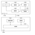
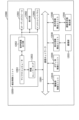
図20は、図19に示すカメラヘッド11102及びCCU11201の機能構成の一例を示すブロック図である。
カメラヘッド11102は、レンズユニット11401と、撮像部11402と、駆動部11403と、通信部11404と、カメラヘッド制御部11405と、を有する。CCU11201は、通信部11411と、画像処理部11412と、制御部11413と、を有する。カメラヘッド11102とCCU11201とは、伝送ケーブル11400によって互いに通信可能に接続されている。
カメラヘッド11102は、レンズユニット11401と、撮像部11402と、駆動部11403と、通信部11404と、カメラヘッド制御部11405と、を有する。CCU11201は、通信部11411と、画像処理部11412と、制御部11413と、を有する。カメラヘッド11102とCCU11201とは、伝送ケーブル11400によって互いに通信可能に接続されている。
レンズユニット11401は、鏡筒11101との接続部に設けられる光学系である。鏡筒11101の先端から取り込まれた観察光は、カメラヘッド11102まで導光され、当該レンズユニット11401に入射する。レンズユニット11401は、ズームレンズ及びフォーカスレンズを含む複数のレンズが組み合わされて構成される。
撮像部11402は、撮像素子で構成される。撮像部11402を構成する撮像素子は、1つ(いわゆる単板式)であってもよいし、複数(いわゆる多板式)であってもよい。撮像部11402が多板式で構成される場合には、例えば各撮像素子によってRGBそれぞれに対応する画像信号が生成され、それらが合成されることによりカラー画像が得られてもよい。あるいは、撮像部11402は、3D(Dimensional)表示に対応する右目用及び左目用の画像信号をそれぞれ取得するための1対の撮像素子を有するように構成されてもよい。3D表示が行われることにより、術者11131は術部における生体組織の奥行きをより正確に把握することが可能になる。なお、撮像部11402が多板式で構成される場合には、各撮像素子に対応して、レンズユニット11401も複数系統設けられ得る。
また、撮像部11402は、必ずしもカメラヘッド11102に設けられなくてもよい。例えば、撮像部11402は、鏡筒11101の内部に、対物レンズの直後に設けられてもよい。
駆動部11403は、アクチュエータによって構成され、カメラヘッド制御部11405からの制御により、レンズユニット11401のズームレンズ及びフォーカスレンズを光軸に沿って所定の距離だけ移動させる。これにより、撮像部11402による撮像画像の倍率及び焦点が適宜調整され得る。
駆動部11403は、アクチュエータによって構成され、カメラヘッド制御部11405からの制御により、レンズユニット11401のズームレンズ及びフォーカスレンズを光軸に沿って所定の距離だけ移動させる。これにより、撮像部11402による撮像画像の倍率及び焦点が適宜調整され得る。
通信部11404は、CCU11201との間で各種の情報を送受信するための通信装置によって構成される。通信部11404は、撮像部11402から得た画像信号をRAWデータとして伝送ケーブル11400を介してCCU11201に送信する。
また、通信部11404は、CCU11201から、カメラヘッド11102の駆動を制御するための制御信号を受信し、カメラヘッド制御部11405に供給する。当該制御信号には、例えば、撮像画像のフレームレートを指定する旨の情報、撮像時の露出値を指定する旨の情報、並びに/又は撮像画像の倍率及び焦点を指定する旨の情報等、撮像条件に関する情報が含まれる。
なお、上記のフレームレートや露出値、倍率、焦点等の撮像条件は、ユーザによって適宜指定されてもよいし、取得された画像信号に基づいてCCU11201の制御部11413によって自動的に設定されてもよい。後者の場合には、いわゆるAE(Auto Exposure)機能、AF(Auto Focus)機能及びAWB(Auto White Balance)機能が内視鏡11100に搭載されていることになる。
カメラヘッド制御部11405は、通信部11404を介して受信したCCU11201からの制御信号に基づいて、カメラヘッド11102の駆動を制御する。
通信部11411は、カメラヘッド11102との間で各種の情報を送受信するための通信装置によって構成される。通信部11411は、カメラヘッド11102から、伝送ケーブル11400を介して送信される画像信号を受信する。
通信部11411は、カメラヘッド11102との間で各種の情報を送受信するための通信装置によって構成される。通信部11411は、カメラヘッド11102から、伝送ケーブル11400を介して送信される画像信号を受信する。
また、通信部11411は、カメラヘッド11102に対して、カメラヘッド11102の駆動を制御するための制御信号を送信する。画像信号や制御信号は、電気通信や光通信等によって送信することができる。
画像処理部11412は、カメラヘッド11102から送信されたRAWデータである画像信号に対して各種の画像処理を施す。
画像処理部11412は、カメラヘッド11102から送信されたRAWデータである画像信号に対して各種の画像処理を施す。
制御部11413は、内視鏡11100による術部等の撮像、及び、術部等の撮像により得られる撮像画像の表示に関する各種の制御を行う。例えば、制御部11413は、カメラヘッド11102の駆動を制御するための制御信号を生成する。
また、制御部11413は、画像処理部11412によって画像処理が施された画像信号に基づいて、術部等が映った撮像画像を表示装置11202に表示させる。この際、制御部11413は、各種の画像認識技術を用いて撮像画像内における各種の物体を認識してもよい。例えば、制御部11413は、撮像画像に含まれる物体のエッジの形状や色等を検出することにより、鉗子等の術具、特定の生体部位、出血、エネルギー処置具11112の使用時のミスト等を認識することができる。制御部11413は、表示装置11202に撮像画像を表示させる際に、その認識結果を用いて、各種の手術支援情報を当該術部の画像に重畳表示させてもよい。手術支援情報が重畳表示され、術者11131に提示されることにより、術者11131の負担を軽減することや、術者11131が確実に手術を進めることが可能になる。
カメラヘッド11102及びCCU11201を接続する伝送ケーブル11400は、電気信号の通信に対応した電気信号ケーブル、光通信に対応した光ファイバ、又はこれらの複合ケーブルである。
ここで、図示する例では、伝送ケーブル11400を用いて有線で通信が行われていたが、カメラヘッド11102とCCU11201との間の通信は無線で行われてもよい。
ここで、図示する例では、伝送ケーブル11400を用いて有線で通信が行われていたが、カメラヘッド11102とCCU11201との間の通信は無線で行われてもよい。
以上、本開示に係る技術が適用され得る内視鏡手術システムの一例について説明した。本開示に係る技術は、以上説明した構成のうち、例えば、内視鏡11100や、カメラヘッド11102の撮像部11402、CCU11201の画像処理部11412等に適用され得る。具体的には、図1の光検出装置1Aは、撮像部10402に適用することができる。
なお、ここでは、一例として内視鏡手術システムについて説明したが、本開示に係る技術は、その他、例えば、顕微鏡手術システム等に適用されてもよい。
なお、ここでは、一例として内視鏡手術システムについて説明したが、本開示に係る技術は、その他、例えば、顕微鏡手術システム等に適用されてもよい。
<移動体への応用例>
本開示に係る技術(本技術)は、様々な製品へ応用することができる。例えば、本開示に係る技術は、自動車、電気自動車、ハイブリッド電気自動車、自動二輪車、自転車、パーソナルモビリティ、飛行機、ドローン、船舶、ロボット等のいずれかの種類の移動体に搭載される装置として実現されてもよい。
本開示に係る技術(本技術)は、様々な製品へ応用することができる。例えば、本開示に係る技術は、自動車、電気自動車、ハイブリッド電気自動車、自動二輪車、自転車、パーソナルモビリティ、飛行機、ドローン、船舶、ロボット等のいずれかの種類の移動体に搭載される装置として実現されてもよい。
図21は、本開示に係る技術が適用され得る移動体制御システムの一例である車両制御システムの概略的な構成例を示すブロック図である。
車両制御システム12000は、通信ネットワーク12001を介して接続された複数の電子制御ユニットを備える。図21に示した例では、車両制御システム12000は、駆動系制御ユニット12010、ボディ系制御ユニット12020、車外情報検出ユニット12030、車内情報検出ユニット12040、及び統合制御ユニット12050を備える。また、統合制御ユニット12050の機能構成として、マイクロコンピュータ12051、音声画像出力部12052、及び車載ネットワークI/F(interface)12053が図示されている。
車両制御システム12000は、通信ネットワーク12001を介して接続された複数の電子制御ユニットを備える。図21に示した例では、車両制御システム12000は、駆動系制御ユニット12010、ボディ系制御ユニット12020、車外情報検出ユニット12030、車内情報検出ユニット12040、及び統合制御ユニット12050を備える。また、統合制御ユニット12050の機能構成として、マイクロコンピュータ12051、音声画像出力部12052、及び車載ネットワークI/F(interface)12053が図示されている。
駆動系制御ユニット12010は、各種プログラムにしたがって車両の駆動系に関連する装置の動作を制御する。例えば、駆動系制御ユニット12010は、内燃機関又は駆動用モータ等の車両の駆動力を発生させるための駆動力発生装置、駆動力を車輪に伝達するための駆動力伝達機構、車両の舵角を調節するステアリング機構、及び、車両の制動力を発生させる制動装置等の制御装置として機能する。
ボディ系制御ユニット12020は、各種プログラムにしたがって車体に装備された各種装置の動作を制御する。例えば、ボディ系制御ユニット12020は、キーレスエントリシステム、スマートキーシステム、パワーウィンドウ装置、あるいは、ヘッドランプ、バックランプ、ブレーキランプ、ウィンカー又はフォグランプ等の各種ランプの制御装置として機能する。この場合、ボディ系制御ユニット12020には、鍵を代替する携帯機から発信される電波又は各種スイッチの信号が入力され得る。ボディ系制御ユニット12020は、これらの電波又は信号の入力を受け付け、車両のドアロック装置、パワーウィンドウ装置、ランプ等を制御する。
車外情報検出ユニット12030は、車両制御システム12000を搭載した車両の外部の情報を検出する。例えば、車外情報検出ユニット12030には、撮像部12031が接続される。車外情報検出ユニット12030は、撮像部12031に車外の画像を撮像させるとともに、撮像された画像を受信する。車外情報検出ユニット12030は、受信した画像に基づいて、人、車、障害物、標識又は路面上の文字等の物体検出処理又は距離検出処理を行ってもよい。
撮像部12031は、光を受光し、その光の受光量に応じた電気信号を出力する光センサである。撮像部12031は、電気信号を画像として出力することもできるし、測距の情報として出力することもできる。また、撮像部12031が受光する光は、可視光であっても良いし、赤外線等の非可視光であっても良い。
車内情報検出ユニット12040は、車内の情報を検出する。車内情報検出ユニット12040には、例えば、運転者の状態を検出する運転者状態検出部12041が接続される。運転者状態検出部12041は、例えば運転者を撮像するカメラを含み、車内情報検出ユニット12040は、運転者状態検出部12041から入力される検出情報に基づいて、運転者の疲労度合い又は集中度合いを算出してもよいし、運転者が居眠りをしていないかを判別してもよい。
マイクロコンピュータ12051は、車外情報検出ユニット12030又は車内情報検出ユニット12040で取得される車内外の情報に基づいて、駆動力発生装置、ステアリング機構又は制動装置の制御目標値を演算し、駆動系制御ユニット12010に対して制御指令を出力することができる。例えば、マイクロコンピュータ12051は、車両の衝突回避あるいは衝撃緩和、車間距離に基づく追従走行、車速維持走行、車両の衝突警告、又は車両のレーン逸脱警告等を含むADAS(Advanced Driver Assistance System)の機能実現を目的とした協調制御を行うことができる。
また、マイクロコンピュータ12051は、車外情報検出ユニット12030又は車内情報検出ユニット12040で取得される車両の周囲の情報に基づいて駆動力発生装置、ステアリング機構又は制動装置等を制御することにより、運転者の操作に拠らずに自律的に走行する自動運転等を目的とした協調制御を行うことができる。
また、マイクロコンピュータ12051は、車外情報検出ユニット12030で取得される車外の情報に基づいて、ボディ系制御ユニット12020に対して制御指令を出力することができる。例えば、マイクロコンピュータ12051は、車外情報検出ユニット12030で検知した先行車又は対向車の位置に応じてヘッドランプを制御し、ハイビームをロービームに切り替える等の防眩を図ることを目的とした協調制御を行うことができる。
音声画像出力部12052は、車両の搭乗者又は車外に対して、視覚的又は聴覚的に情報を通知することが可能な出力装置へ音声及び画像のうちの少なくとも一方の出力信号を送信する。図21の例では、出力装置として、オーディオスピーカ12061、表示部12062及びインストルメントパネル12063が例示されている。表示部12062は、例えば、オンボードディスプレイ及びヘッドアップディスプレイの少なくとも一つを含んでいてもよい。
図22は、撮像部12031の設置位置の例を示す図である。
図22では、車両12100は、撮像部12031として、撮像部12101,12102,12103,12104,12105を有する。
図22では、車両12100は、撮像部12031として、撮像部12101,12102,12103,12104,12105を有する。
撮像部12101,12102,12103,12104,12105は、例えば、車両12100のフロントノーズ、サイドミラー、リアバンパ、バックドア及び車室内のフロントガラスの上部等の位置に設けられる。フロントノーズに備えられる撮像部12101及び車室内のフロントガラスの上部に備えられる撮像部12105は、主として車両12100の前方の画像を取得する。サイドミラーに備えられる撮像部12102,12103は、主として車両12100の側方の画像を取得する。リアバンパ又はバックドアに備えられる撮像部12104は、主として車両12100の後方の画像を取得する。撮像部12101及び12105で取得される前方の画像は、主として先行車両又は、歩行者、障害物、信号機、交通標識又は車線等の検出に用いられる。
なお、図22には、撮像部12101ないし12104の撮影範囲の一例が示されている。撮像範囲12111は、フロントノーズに設けられた撮像部12101の撮像範囲を示し、撮像範囲12112,12113は、それぞれサイドミラーに設けられた撮像部12102,12103の撮像範囲を示し、撮像範囲12114は、リアバンパ又はバックドアに設けられた撮像部12104の撮像範囲を示す。例えば、撮像部12101ないし12104で撮像された画像データが重ね合わせられることにより、車両12100を上方から見た俯瞰画像が得られる。
撮像部12101ないし12104の少なくとも1つは、距離情報を取得する機能を有していてもよい。例えば、撮像部12101ないし12104の少なくとも1つは、複数の撮像素子からなるステレオカメラであってもよいし、位相差検出用の画素を有する撮像素子であってもよい。
例えば、マイクロコンピュータ12051は、撮像部12101ないし12104から得られた距離情報を基に、撮像範囲12111ないし12114内における各立体物までの距離と、この距離の時間的変化(車両12100に対する相対速度)を求めることにより、特に車両12100の進行路上にある最も近い立体物で、車両12100と略同じ方向に所定の速度(例えば、0km/h以上)で走行する立体物を先行車として抽出することができる。さらに、マイクロコンピュータ12051は、先行車の手前に予め確保すべき車間距離を設定し、自動ブレーキ制御(追従停止制御も含む)や自動加速制御(追従発進制御も含む)等を行うことができる。このように運転者の操作に拠らずに自律的に走行する自動運転等を目的とした協調制御を行うことができる。
例えば、マイクロコンピュータ12051は、撮像部12101ないし12104から得られた距離情報を元に、立体物に関する立体物データを、2輪車、普通車両、大型車両、歩行者、電柱等その他の立体物に分類して抽出し、障害物の自動回避に用いることができる。例えば、マイクロコンピュータ12051は、車両12100の周辺の障害物を、車両12100のドライバが視認可能な障害物と視認困難な障害物とに識別する。そして、マイクロコンピュータ12051は、各障害物との衝突の危険度を示す衝突リスクを判断し、衝突リスクが設定値以上で衝突可能性がある状況であるときには、オーディオスピーカ12061や表示部12062を介してドライバに警報を出力することや、駆動系制御ユニット12010を介して強制減速や回避操舵を行うことで、衝突回避のための運転支援を行うことができる。
撮像部12101ないし12104の少なくとも1つは、赤外線を検出する赤外線カメラであってもよい。例えば、マイクロコンピュータ12051は、撮像部12101ないし12104の撮像画像中に歩行者が存在するか否かを判定することで歩行者を認識することができる。かかる歩行者の認識は、例えば赤外線カメラとしての撮像部12101ないし12104の撮像画像における特徴点を抽出する手順と、物体の輪郭を示す一連の特徴点にパターンマッチング処理を行って歩行者か否かを判別する手順によって行われる。マイクロコンピュータ12051が、撮像部12101ないし12104の撮像画像中に歩行者が存在すると判定し、歩行者を認識すると、音声画像出力部12052は、当該認識された歩行者に強調のための方形輪郭線を重畳表示するように、表示部12062を制御する。また、音声画像出力部12052は、歩行者を示すアイコン等を所望の位置に表示するように表示部12062を制御してもよい。
以上、本開示に係る技術が適用され得る車両制御システムの一例について説明した。本開示に係る技術は、以上説明した構成のうち、例えば、撮像部12031等に適用され得る。具体的には、図1の光検出装置1Aに適用することができる。
なお、本開示は以下のような構成も取ることができる。
(1)
光が入射する受光面及び前記受光面の反対側に位置する素子形成面を有する半導体層と、
前記半導体層に行列状に配置され、前記受光面から入射した光に応じて電気信号を生成可能な複数の画素と、
前記半導体層の前記受光面から前記素子形成面への深さ方向に延伸し、隣接する前記画素の間を分離する画素分離部と、
を備え、
前記画素分離部は、平面視において、行方向または列方向へ延伸され、第1の深さを有する掘り込み領域を第1の線幅で形成され、前記第1の深さと異なる第2の深さを有する掘り込み領域を、前記第1の深さの掘り込み領域に合わせるように、前記第1の線幅とは異なる第2の線幅で形成される、光検出装置。
(2)
前記画素分離部は、前記第2の深さが前記第1の深さより浅い場合に、前記第2の線幅を前記第1の線幅より太く形成される、(1)に記載の光検出装置。
(3)
前記画素分離部は、前記第2の深さが前記第1の深さより深い場合に、前記第2の線幅を前記第1の線幅より細く形成される、(1)に記載の光検出装置。
(4)
前記画素分離部は、行方向に延伸される前記第1の線幅の掘り込み領域と列方向に延伸される前記第1の線幅の掘り込み領域とが交差する領域を有し、平面視において、前記交差する領域の線幅が、前記第1の線幅よりも細く形成される、(1)に記載の光検出装置。
(5)
前記画素分離部の前記交差する領域は、前記行方向に延伸される第1の領域と、前記列方向に延伸される第2の領域とを有し、
前記第1の領域及び前記第2の領域は、別々に形成される、(4)に記載の光検出装置。
(6)
前記第1の領域は、前記第2の領域と交差する箇所以外の前記第1の線幅となる両端に、前記掘り込み領域の埋め込み膜を除去するための開口パターンをそれぞれ形成し、
前記第2の領域は、前記第1の領域と交差する箇所以外の前記第1の線幅となる両端に、前記掘り込み領域の埋め込み膜を除去するための開口パターンをそれぞれ形成する、(5)に記載の光検出装置。
(7)
前記画素分離部から前記半導体層の厚み方向に垂直な方向に沿って延在した遮光部を備え、
前記遮光部は、前記画素分離部の前記第1の深さの掘り込み領域において、第1の厚みを有し、前記第2の深さの掘り込み領域において、前記第1の厚みとは異なる第2の厚みを有する場合に、前記第2の厚みを前記第1の厚みに合わせるように形成される、(1)に記載の光検出装置。
(8)
前記複数の画素のそれぞれは、
前記半導体層の厚み方向において前記遮光部から受光面側に位置し、前記受光面から入射した光を光電変換して電荷を生成する光電変換部と、
前記半導体層の厚み方向において前記遮光部から素子形成面側に位置し、前記光電変換部から転送される電荷を保持する電荷保持部と、
を備える、(7)に記載の光検出装置。
(9)
前記複数の画素のそれぞれは、前記光電変換部に達する垂直ゲート電極を有し、前記光電変換部から前記電荷保持部に電荷を転送する転送トランジスタを備え、
前記遮光部は、前記垂直ゲート電極が貫通する開口部を有する、(8)に記載の光検出装置。
(10)
前記複数の画素のそれぞれは、前記遮光部の開口部のうち電荷保持部寄りの端縁と前記垂直ゲート電極との間に介した、前記転送トランジスタへの電荷の転送を遮る遮電荷部を有する、(9)に記載の光検出装置。
(11)
前記画素分離部に埋め込む膜種は、シリコン系膜種である、(1)に記載の光検出装置。
(12)
前記画素分離部に埋め込む膜種は、メタル系膜種である、(1)に記載の光検出装置。
(13)
前記画素分離部は、前記第1の線幅より太い線幅の掘り込み領域に形成されるハードマスク開口パターンを有する、(1)に記載の光検出装置。
(14)
光が入射する受光面及び前記受光面の反対側に位置する素子形成面を有する半導体層と、前記半導体層に行列状に配置され、前記受光面から入射した光に応じて電気信号を生成可能な複数の画素と、前記半導体層の前記受光面から前記素子形成面への深さ方向に延伸し、隣接する前記画素の間を分離する画素分離部と、を備える光検出装置の製造方法であって、
平面視において、行方向または列方向へ延伸される前記画素分離部の、第1の深さを有する掘り込み領域を第1の線幅で形成することと、
前記第1の深さと異なる第2の深さを有する掘り込み領域を、前記第1の深さの掘り込み領域に合わせるように、前記第1の線幅とは異なる第2の線幅で形成することと、
前記掘り込み領域内に、埋め込み膜を形成することと、
前記掘り込み領域のうち前記第1の線幅より太い線幅の掘り込み領域にハードマスク開口パターンを形成することと、
前記ハードマスク開口パターンに基づいて、前記掘り込み領域内の前記埋め込み膜を除去することと、
を備える、光検出装置の製造方法。
(15)
光が入射する受光面及び前記受光面の反対側に位置する素子形成面を有する半導体層と、
前記半導体層に行列状に配置され、前記受光面から入射した光に応じて電気信号を生成可能な複数の画素と、
前記半導体層の前記受光面から前記素子形成面への深さ方向に延伸し、隣接する前記画
素の間を分離する画素分離部と、
を備え、
前記画素分離部は、平面視において、行方向または列方向へ延伸され、第1の深さを有する掘り込み領域を第1の線幅で形成され、前記第1の深さと異なる第2の深さを有する掘り込み領域を、前記第1の深さの掘り込み領域に合わせるように、前記第1の線幅とは異なる第2の線幅で形成される、光検出装置を備えた、
電子機器。
(1)
光が入射する受光面及び前記受光面の反対側に位置する素子形成面を有する半導体層と、
前記半導体層に行列状に配置され、前記受光面から入射した光に応じて電気信号を生成可能な複数の画素と、
前記半導体層の前記受光面から前記素子形成面への深さ方向に延伸し、隣接する前記画素の間を分離する画素分離部と、
を備え、
前記画素分離部は、平面視において、行方向または列方向へ延伸され、第1の深さを有する掘り込み領域を第1の線幅で形成され、前記第1の深さと異なる第2の深さを有する掘り込み領域を、前記第1の深さの掘り込み領域に合わせるように、前記第1の線幅とは異なる第2の線幅で形成される、光検出装置。
(2)
前記画素分離部は、前記第2の深さが前記第1の深さより浅い場合に、前記第2の線幅を前記第1の線幅より太く形成される、(1)に記載の光検出装置。
(3)
前記画素分離部は、前記第2の深さが前記第1の深さより深い場合に、前記第2の線幅を前記第1の線幅より細く形成される、(1)に記載の光検出装置。
(4)
前記画素分離部は、行方向に延伸される前記第1の線幅の掘り込み領域と列方向に延伸される前記第1の線幅の掘り込み領域とが交差する領域を有し、平面視において、前記交差する領域の線幅が、前記第1の線幅よりも細く形成される、(1)に記載の光検出装置。
(5)
前記画素分離部の前記交差する領域は、前記行方向に延伸される第1の領域と、前記列方向に延伸される第2の領域とを有し、
前記第1の領域及び前記第2の領域は、別々に形成される、(4)に記載の光検出装置。
(6)
前記第1の領域は、前記第2の領域と交差する箇所以外の前記第1の線幅となる両端に、前記掘り込み領域の埋め込み膜を除去するための開口パターンをそれぞれ形成し、
前記第2の領域は、前記第1の領域と交差する箇所以外の前記第1の線幅となる両端に、前記掘り込み領域の埋め込み膜を除去するための開口パターンをそれぞれ形成する、(5)に記載の光検出装置。
(7)
前記画素分離部から前記半導体層の厚み方向に垂直な方向に沿って延在した遮光部を備え、
前記遮光部は、前記画素分離部の前記第1の深さの掘り込み領域において、第1の厚みを有し、前記第2の深さの掘り込み領域において、前記第1の厚みとは異なる第2の厚みを有する場合に、前記第2の厚みを前記第1の厚みに合わせるように形成される、(1)に記載の光検出装置。
(8)
前記複数の画素のそれぞれは、
前記半導体層の厚み方向において前記遮光部から受光面側に位置し、前記受光面から入射した光を光電変換して電荷を生成する光電変換部と、
前記半導体層の厚み方向において前記遮光部から素子形成面側に位置し、前記光電変換部から転送される電荷を保持する電荷保持部と、
を備える、(7)に記載の光検出装置。
(9)
前記複数の画素のそれぞれは、前記光電変換部に達する垂直ゲート電極を有し、前記光電変換部から前記電荷保持部に電荷を転送する転送トランジスタを備え、
前記遮光部は、前記垂直ゲート電極が貫通する開口部を有する、(8)に記載の光検出装置。
(10)
前記複数の画素のそれぞれは、前記遮光部の開口部のうち電荷保持部寄りの端縁と前記垂直ゲート電極との間に介した、前記転送トランジスタへの電荷の転送を遮る遮電荷部を有する、(9)に記載の光検出装置。
(11)
前記画素分離部に埋め込む膜種は、シリコン系膜種である、(1)に記載の光検出装置。
(12)
前記画素分離部に埋め込む膜種は、メタル系膜種である、(1)に記載の光検出装置。
(13)
前記画素分離部は、前記第1の線幅より太い線幅の掘り込み領域に形成されるハードマスク開口パターンを有する、(1)に記載の光検出装置。
(14)
光が入射する受光面及び前記受光面の反対側に位置する素子形成面を有する半導体層と、前記半導体層に行列状に配置され、前記受光面から入射した光に応じて電気信号を生成可能な複数の画素と、前記半導体層の前記受光面から前記素子形成面への深さ方向に延伸し、隣接する前記画素の間を分離する画素分離部と、を備える光検出装置の製造方法であって、
平面視において、行方向または列方向へ延伸される前記画素分離部の、第1の深さを有する掘り込み領域を第1の線幅で形成することと、
前記第1の深さと異なる第2の深さを有する掘り込み領域を、前記第1の深さの掘り込み領域に合わせるように、前記第1の線幅とは異なる第2の線幅で形成することと、
前記掘り込み領域内に、埋め込み膜を形成することと、
前記掘り込み領域のうち前記第1の線幅より太い線幅の掘り込み領域にハードマスク開口パターンを形成することと、
前記ハードマスク開口パターンに基づいて、前記掘り込み領域内の前記埋め込み膜を除去することと、
を備える、光検出装置の製造方法。
(15)
光が入射する受光面及び前記受光面の反対側に位置する素子形成面を有する半導体層と、
前記半導体層に行列状に配置され、前記受光面から入射した光に応じて電気信号を生成可能な複数の画素と、
前記半導体層の前記受光面から前記素子形成面への深さ方向に延伸し、隣接する前記画
素の間を分離する画素分離部と、
を備え、
前記画素分離部は、平面視において、行方向または列方向へ延伸され、第1の深さを有する掘り込み領域を第1の線幅で形成され、前記第1の深さと異なる第2の深さを有する掘り込み領域を、前記第1の深さの掘り込み領域に合わせるように、前記第1の線幅とは異なる第2の線幅で形成される、光検出装置を備えた、
電子機器。
1A,1B 光検出装置
2 半導体チップ
2A 画素アレイ部
2B 周辺部
2C パッド配置部
3 画素
4 垂直駆動回路
5 カラム信号処理回路
6 水平駆動回路
7 出力回路
8 制御回路
10 画素駆動配線、
11 垂直信号線
12 水平信号線
13 ロジック回路
14 ボンディングパッド
20 半導体層
20x1,20y1 第1側面部
20x2,20y2 第2側面部
21 p型のウエル領域
22 トレンチ
23 絶縁膜
24 分離領域
24x 第1部分
24y 第2部分
24x1,24x2,24y1,24y2 領域
25 交差箇所
26 非分離領域
27 光電変換領域
30 多層配線層
30-1 第1基板
31 層間絶縁膜
31-1,41-1 半導体基板
31A-1 受光面
31B-1 形成面
31C-1 半導体部
31D-1,31E-1,31F-1 結晶面
32 配線
32-1 絶縁層
32A N型半導体領域
32A-1,32B-1 N型半導体領域
33-1 半導体層
33s-1 サイドウォール
34 支持基板
34-1,36-1 素子分離部
34A-1,35-1 埋め込み部
34B-1 P型半導体部
36 平坦化膜
36A-1 金属埋め込み部
36B-1,37B-1 絶縁膜
37-1 遮光部
37H-1 開口
38 接着膜
38-1 固定電荷膜
39-1 カラーフィルタ
40 カラーフィルタ層
40-1 第2基板
41 第1カラーフィルタ部
42 第2カラーフィルタ部
43 第3カラーフィルタ部
45 マイクロレンズ
50 ストッパー層
50-1 受光レンズ
51 第1の酸化シリコン膜
51-1,53-1 空洞部
52 窒化シリコン膜
53 第2の酸化シリコン膜
54 アクティブパターン
56 素子分離部(STI)
61 絶縁膜
62 塗布膜
63 反射防止膜
64,71,81,83 レジスト
72 ホール
82,84 開口部
110-1 ハードマスク
111 シリコン
551,552 凸部
2201 撮像装置
2202 光学系
2203 シャッタ装置
2204 固体撮像素子
2205 制御回路
2206 信号処理回路
2207 モニタ
2208 メモリ
10402 撮像部
11000 内視鏡手術システム
11100 内視鏡
11101 鏡筒
11102 カメラヘッド
11110 術具
11111 気腹チューブ
11112 エネルギー処置具
11120 支持アーム装置
11131 術者(医師)
11132 患者
11133 患者ベッド
11200 カート
11201 カメラコントロールユニット(CCU: Camera Control Unit)
11202 表示装置
11203 光源装置
11204 入力装置
11205 処置具制御装置
11206 気腹装置
11207 レコーダ
11208 プリンタ
11400 伝送ケーブル
11401 レンズユニット
11402 撮像部
11403 駆動部
11404 通信部
11405 カメラヘッド制御部
11411 通信部
11412 画像処理部
11413 制御部
12000 車両制御システム
12001 通信ネットワーク
12010 駆動系制御ユニット
12020 ボディ系制御ユニット
12030 車外情報検出ユニット
12031 撮像部
12040 車内情報検出ユニット
12041 運転者状態検出部
12050 統合制御ユニット
12051 マイクロコンピュータ
12052 音声画像出力部
12061 オーディオスピーカ
12062 表示部
12063 インストルメントパネル
12100 車両
12101~12105 撮像部
12111~12114 撮像範囲
2 半導体チップ
2A 画素アレイ部
2B 周辺部
2C パッド配置部
3 画素
4 垂直駆動回路
5 カラム信号処理回路
6 水平駆動回路
7 出力回路
8 制御回路
10 画素駆動配線、
11 垂直信号線
12 水平信号線
13 ロジック回路
14 ボンディングパッド
20 半導体層
20x1,20y1 第1側面部
20x2,20y2 第2側面部
21 p型のウエル領域
22 トレンチ
23 絶縁膜
24 分離領域
24x 第1部分
24y 第2部分
24x1,24x2,24y1,24y2 領域
25 交差箇所
26 非分離領域
27 光電変換領域
30 多層配線層
30-1 第1基板
31 層間絶縁膜
31-1,41-1 半導体基板
31A-1 受光面
31B-1 形成面
31C-1 半導体部
31D-1,31E-1,31F-1 結晶面
32 配線
32-1 絶縁層
32A N型半導体領域
32A-1,32B-1 N型半導体領域
33-1 半導体層
33s-1 サイドウォール
34 支持基板
34-1,36-1 素子分離部
34A-1,35-1 埋め込み部
34B-1 P型半導体部
36 平坦化膜
36A-1 金属埋め込み部
36B-1,37B-1 絶縁膜
37-1 遮光部
37H-1 開口
38 接着膜
38-1 固定電荷膜
39-1 カラーフィルタ
40 カラーフィルタ層
40-1 第2基板
41 第1カラーフィルタ部
42 第2カラーフィルタ部
43 第3カラーフィルタ部
45 マイクロレンズ
50 ストッパー層
50-1 受光レンズ
51 第1の酸化シリコン膜
51-1,53-1 空洞部
52 窒化シリコン膜
53 第2の酸化シリコン膜
54 アクティブパターン
56 素子分離部(STI)
61 絶縁膜
62 塗布膜
63 反射防止膜
64,71,81,83 レジスト
72 ホール
82,84 開口部
110-1 ハードマスク
111 シリコン
551,552 凸部
2201 撮像装置
2202 光学系
2203 シャッタ装置
2204 固体撮像素子
2205 制御回路
2206 信号処理回路
2207 モニタ
2208 メモリ
10402 撮像部
11000 内視鏡手術システム
11100 内視鏡
11101 鏡筒
11102 カメラヘッド
11110 術具
11111 気腹チューブ
11112 エネルギー処置具
11120 支持アーム装置
11131 術者(医師)
11132 患者
11133 患者ベッド
11200 カート
11201 カメラコントロールユニット(CCU: Camera Control Unit)
11202 表示装置
11203 光源装置
11204 入力装置
11205 処置具制御装置
11206 気腹装置
11207 レコーダ
11208 プリンタ
11400 伝送ケーブル
11401 レンズユニット
11402 撮像部
11403 駆動部
11404 通信部
11405 カメラヘッド制御部
11411 通信部
11412 画像処理部
11413 制御部
12000 車両制御システム
12001 通信ネットワーク
12010 駆動系制御ユニット
12020 ボディ系制御ユニット
12030 車外情報検出ユニット
12031 撮像部
12040 車内情報検出ユニット
12041 運転者状態検出部
12050 統合制御ユニット
12051 マイクロコンピュータ
12052 音声画像出力部
12061 オーディオスピーカ
12062 表示部
12063 インストルメントパネル
12100 車両
12101~12105 撮像部
12111~12114 撮像範囲
Claims (15)
- 光が入射する受光面及び前記受光面の反対側に位置する素子形成面を有する半導体層と、
前記半導体層に行列状に配置され、前記受光面から入射した光に応じて電気信号を生成可能な複数の画素と、
前記半導体層の前記受光面から前記素子形成面への深さ方向に延伸し、隣接する前記画素の間を分離する画素分離部と、
を備え、
前記画素分離部は、平面視において、行方向または列方向へ延伸され、第1の深さを有する掘り込み領域を第1の線幅で形成され、前記第1の深さと異なる第2の深さを有する掘り込み領域を、前記第1の深さの掘り込み領域に合わせるように、前記第1の線幅とは異なる第2の線幅で形成される、光検出装置。 - 前記画素分離部は、前記第2の深さが前記第1の深さより浅い場合に、前記第2の線幅を前記第1の線幅より太く形成される、請求項1に記載の光検出装置。
- 前記画素分離部は、前記第2の深さが前記第1の深さより深い場合に、前記第2の線幅を前記第1の線幅より細く形成される、請求項1に記載の光検出装置。
- 前記画素分離部は、行方向に延伸される前記第1の線幅の掘り込み領域と列方向に延伸される前記第1の線幅の掘り込み領域とが交差する領域を有し、平面視において、前記交差する領域の線幅が、前記第1の線幅よりも細く形成される、請求項1に記載の光検出装置。
- 前記画素分離部の前記交差する領域は、前記行方向に延伸される第1の領域と、前記列方向に延伸される第2の領域とを有し、
前記第1の領域及び前記第2の領域は、別々に形成される、請求項4に記載の光検出装置。 - 前記第1の領域は、前記第2の領域と交差する箇所以外の前記第1の線幅となる両端に、前記掘り込み領域の埋め込み膜を除去するための開口パターンをそれぞれ形成し、
前記第2の領域は、前記第1の領域と交差する箇所以外の前記第1の線幅となる両端に、前記掘り込み領域の埋め込み膜を除去するための開口パターンをそれぞれ形成する、請求項5に記載の光検出装置。 - 前記画素分離部から前記半導体層の厚み方向に垂直な方向に沿って延在した遮光部を備え、
前記遮光部は、前記画素分離部の前記第1の深さの掘り込み領域において、第1の厚みを有し、前記第2の深さの掘り込み領域において、前記第1の厚みとは異なる第2の厚みを有する場合に、前記第2の厚みを前記第1の厚みに合わせるように形成される、請求項1に記載の光検出装置。 - 前記複数の画素のそれぞれは、
前記半導体層の厚み方向において前記遮光部から受光面側に位置し、前記受光面から入射した光を光電変換して電荷を生成する光電変換部と、
前記半導体層の厚み方向において前記遮光部から素子形成面側に位置し、前記光電変換部から転送される電荷を保持する電荷保持部と、
を備える、請求項7に記載の光検出装置。 - 前記複数の画素のそれぞれは、前記光電変換部に達する垂直ゲート電極を有し、前記光電変換部から前記電荷保持部に電荷を転送する転送トランジスタを備え、
前記遮光部は、前記垂直ゲート電極が貫通する開口部を有する、請求項8に記載の光検出装置。 - 前記複数の画素のそれぞれは、前記遮光部の開口部のうち電荷保持部寄りの端縁と前記垂直ゲート電極との間に介した、前記転送トランジスタへの電荷の転送を遮る遮電荷部を有する、請求項9に記載の光検出装置。
- 前記画素分離部に埋め込む膜種は、シリコン系膜種である、請求項1に記載の光検出装置。
- 前記画素分離部に埋め込む膜種は、メタル系膜種である、請求項1に記載の光検出装置。
- 前記画素分離部は、前記第1の線幅より太い線幅の掘り込み領域に形成されるハードマスク開口パターンを有する、請求項1に記載の光検出装置。
- 光が入射する受光面及び前記受光面の反対側に位置する素子形成面を有する半導体層と、前記半導体層に行列状に配置され、前記受光面から入射した光に応じて電気信号を生成可能な複数の画素と、前記半導体層の前記受光面から前記素子形成面への深さ方向に延伸し、隣接する前記画素の間を分離する画素分離部と、を備える光検出装置の製造方法であって、
平面視において、行方向または列方向へ延伸される前記画素分離部の、第1の深さを有する掘り込み領域を第1の線幅で形成することと、
前記第1の深さと異なる第2の深さを有する掘り込み領域を、前記第1の深さの掘り込み領域に合わせるように、前記第1の線幅とは異なる第2の線幅で形成することと、
前記掘り込み領域内に、埋め込み膜を形成することと、
前記掘り込み領域のうち前記第1の線幅より太い線幅の掘り込み領域にハードマスク開口パターンを形成することと、
前記ハードマスク開口パターンに基づいて、前記掘り込み領域内の前記埋め込み膜を除去することと、
を備える、光検出装置の製造方法。 - 光が入射する受光面及び前記受光面の反対側に位置する素子形成面を有する半導体層と、
前記半導体層に行列状に配置され、前記受光面から入射した光に応じて電気信号を生成可能な複数の画素と、
前記半導体層の前記受光面から前記素子形成面への深さ方向に延伸し、隣接する前記画素の間を分離する画素分離部と、
を備え、
前記画素分離部は、平面視において、行方向または列方向へ延伸され、第1の深さを有する掘り込み領域を第1の線幅で形成され、前記第1の深さと異なる第2の深さを有する掘り込み領域を、前記第1の深さの掘り込み領域に合わせるように、前記第1の線幅とは異なる第2の線幅で形成される、光検出装置を備えた、
電子機器。
Applications Claiming Priority (2)
| Application Number | Priority Date | Filing Date | Title |
|---|---|---|---|
| JP2023-218414 | 2023-12-25 | ||
| JP2023218414 | 2023-12-25 |
Publications (1)
| Publication Number | Publication Date |
|---|---|
| WO2025142145A1 true WO2025142145A1 (ja) | 2025-07-03 |
Family
ID=96218850
Family Applications (1)
| Application Number | Title | Priority Date | Filing Date |
|---|---|---|---|
| PCT/JP2024/039692 Pending WO2025142145A1 (ja) | 2023-12-25 | 2024-11-07 | 光検出装置、光検出装置の製造方法及び電子機器 |
Country Status (1)
| Country | Link |
|---|---|
| WO (1) | WO2025142145A1 (ja) |
Citations (5)
| Publication number | Priority date | Publication date | Assignee | Title |
|---|---|---|---|---|
| JP2014033107A (ja) * | 2012-08-03 | 2014-02-20 | Sony Corp | 固体撮像装置、固体撮像装置の製造方法及び電子機器 |
| US20160099267A1 (en) * | 2014-10-02 | 2016-04-07 | Samsung Electronics Co., Ltd. | Cmos image sensor for reducing dead zone |
| WO2020137370A1 (ja) * | 2018-12-27 | 2020-07-02 | ソニーセミコンダクタソリューションズ株式会社 | 固体撮像装置および電子機器 |
| JP2021034598A (ja) * | 2019-08-27 | 2021-03-01 | ソニーセミコンダクタソリューションズ株式会社 | 撮像素子、製造方法、および電子機器 |
| US20220246658A1 (en) * | 2021-02-04 | 2022-08-04 | Hua Hong Semiconductor (Wuxi) Limited | Image sensor and method for making the same |
-
2024
- 2024-11-07 WO PCT/JP2024/039692 patent/WO2025142145A1/ja active Pending
Patent Citations (5)
| Publication number | Priority date | Publication date | Assignee | Title |
|---|---|---|---|---|
| JP2014033107A (ja) * | 2012-08-03 | 2014-02-20 | Sony Corp | 固体撮像装置、固体撮像装置の製造方法及び電子機器 |
| US20160099267A1 (en) * | 2014-10-02 | 2016-04-07 | Samsung Electronics Co., Ltd. | Cmos image sensor for reducing dead zone |
| WO2020137370A1 (ja) * | 2018-12-27 | 2020-07-02 | ソニーセミコンダクタソリューションズ株式会社 | 固体撮像装置および電子機器 |
| JP2021034598A (ja) * | 2019-08-27 | 2021-03-01 | ソニーセミコンダクタソリューションズ株式会社 | 撮像素子、製造方法、および電子機器 |
| US20220246658A1 (en) * | 2021-02-04 | 2022-08-04 | Hua Hong Semiconductor (Wuxi) Limited | Image sensor and method for making the same |
Similar Documents
| Publication | Publication Date | Title |
|---|---|---|
| JP7586709B2 (ja) | 固体撮像装置および電子機器 | |
| US20230411429A1 (en) | Imaging device and light-receiving element | |
| WO2023042462A1 (ja) | 光検出装置、光検出装置の製造方法、及び電子機器 | |
| JP7520499B2 (ja) | 半導体素子および電子機器 | |
| JP7677899B2 (ja) | 撮像素子および撮像装置 | |
| JP7503399B2 (ja) | 固体撮像装置及びその製造方法、並びに電子機器 | |
| JP7562250B2 (ja) | 半導体素子および電子機器 | |
| WO2024262205A1 (ja) | 半導体装置 | |
| WO2024202617A1 (ja) | 半導体装置、光検出装置及び半導体装置の製造方法 | |
| WO2023210238A1 (ja) | 光検出装置及び電子機器 | |
| WO2025142145A1 (ja) | 光検出装置、光検出装置の製造方法及び電子機器 | |
| JP7802812B2 (ja) | 撮像装置及び電子機器 | |
| JP7759387B2 (ja) | 固体撮像装置およびその製造方法 | |
| WO2025028016A1 (ja) | 半導体装置、半導体装置の製造方法及び光検出装置 | |
| US20250142999A1 (en) | Photodetector and method of manufacturing photodetector | |
| WO2025028015A1 (ja) | 光検出装置及び半導体装置 | |
| WO2025084263A1 (ja) | 光検出装置および固体撮像装置 | |
| WO2025028020A1 (ja) | 半導体装置及び光検出装置 | |
| WO2024154666A1 (ja) | 半導体装置 | |
| WO2024202616A1 (ja) | 光検出装置、光検出装置の製造方法及び電子機器 | |
| WO2025069737A1 (ja) | 光検出装置及び電子機器 | |
| WO2025197315A1 (ja) | 光検出装置及び電子機器 | |
| WO2025028017A1 (ja) | 光検出装置及び電子機器 | |
| WO2026038469A1 (ja) | 半導体装置、光検出装置および電子機器 | |
| WO2025079337A1 (ja) | 光検出装置及び電子機器 |
Legal Events
| Date | Code | Title | Description |
|---|---|---|---|
| 121 | Ep: the epo has been informed by wipo that ep was designated in this application |
Ref document number: 24912038 Country of ref document: EP Kind code of ref document: A1 |