WO2025142111A1 - 電波反射板および電波反射装置 - Google Patents
電波反射板および電波反射装置 Download PDFInfo
- Publication number
- WO2025142111A1 WO2025142111A1 PCT/JP2024/038699 JP2024038699W WO2025142111A1 WO 2025142111 A1 WO2025142111 A1 WO 2025142111A1 JP 2024038699 W JP2024038699 W JP 2024038699W WO 2025142111 A1 WO2025142111 A1 WO 2025142111A1
- Authority
- WO
- WIPO (PCT)
- Prior art keywords
- radio wave
- ground electrode
- electrode
- region
- reflecting
- Prior art date
- Legal status (The legal status is an assumption and is not a legal conclusion. Google has not performed a legal analysis and makes no representation as to the accuracy of the status listed.)
- Pending
Links
Images




Classifications
-
- H—ELECTRICITY
- H01—ELECTRIC ELEMENTS
- H01Q—ANTENNAS, i.e. RADIO AERIALS
- H01Q13/00—Waveguide horns or mouths; Slot antennas; Leaky-waveguide antennas; Equivalent structures causing radiation along the transmission path of a guided wave
- H01Q13/08—Radiating ends of two-conductor microwave transmission lines, e.g. of coaxial lines, of microstrip lines
-
- H—ELECTRICITY
- H01—ELECTRIC ELEMENTS
- H01Q—ANTENNAS, i.e. RADIO AERIALS
- H01Q15/00—Devices for reflection, refraction, diffraction or polarisation of waves radiated from an antenna, e.g. quasi-optical devices
- H01Q15/14—Reflecting surfaces; Equivalent structures
-
- H—ELECTRICITY
- H01—ELECTRIC ELEMENTS
- H01Q—ANTENNAS, i.e. RADIO AERIALS
- H01Q21/00—Antenna arrays or systems
- H01Q21/06—Arrays of individually energised antenna units similarly polarised and spaced apart
Definitions
- the antenna elements of the phased array antenna device in Patent Document 1 have multiple strip wirings, a planar electrode facing the multiple strip wirings, and a liquid crystal layer provided between the multiple strip wirings and the planar electrode. Different voltages are applied to the multiple strip wirings in the multiple antenna elements.
- the phase can be changed by adjusting the dielectric constant of the liquid crystal layer for each antenna element and superimposing the reflected waves. This makes it possible to set the reflection direction of the radio waves in any direction.
- one embodiment of the present invention has an object to provide a transparent radio wave reflector that improves visibility at the boundaries between radio wave reflectors when multiple radio wave reflectors are combined and arranged. Also, one embodiment of the present invention has an object to provide a radio wave reflecting device in which multiple transparent radio wave reflectors are combined and arranged, improving visibility at the boundaries between the radio wave reflectors.
- the radio wave reflector includes a patch electrode on a first substrate, a ground electrode on a second substrate different from the first substrate, a liquid crystal layer between the patch electrode and the ground electrode, a reflective antenna region in which the patch electrode and the ground electrode overlap in a planar view, and a peripheral region in which only the ground electrode is provided, surrounding the reflective antenna region in a planar view, and each of the patch electrode and the ground electrode includes a plurality of openings.
- each of the first radio wave reflector and the second radio wave reflector includes a patch electrode on a first substrate, a ground electrode on a second substrate different from the first substrate, a liquid crystal layer between the patch electrode and the ground electrode, a reflective antenna region in which the patch electrode and the ground electrode overlap in a planar view, and a peripheral region surrounding the reflective antenna region in which only the ground electrode is provided in a planar view, and each of the patch electrode and the ground electrode includes a plurality of openings, and the peripheral region of the first radio wave reflector is in contact with the peripheral region of the second radio wave reflector.
- FIG. 1 is a schematic plan view showing an outline of the configuration of a radio wave reflecting device according to an embodiment of the present invention
- 1 is a schematic plan view showing an outline of the configuration of a radio wave reflector according to one embodiment of the present invention
- 1 is a schematic cross-sectional view showing the configuration of a reflective antenna cell of a radio wave reflector according to one embodiment of the present invention and the direction in which radio waves are reflected by the reflective antenna cell.
- 1 is a schematic plan view showing the configuration of a reflecting antenna region and a peripheral region of a radio wave reflecting plate according to an embodiment of the present invention.
- FIG. 1 is a schematic plan view showing the configuration of a reflecting antenna region and a peripheral region of a radio wave reflecting plate according to an embodiment of the present invention.
- FIG. 1 is a schematic plan view showing the configuration of a reflecting antenna region and a peripheral region of a radio wave reflecting plate according to an embodiment of the present invention.
- two components being “substantially identical” means that the two components are different in size but have the same shape, the difference in area between the two components is within ⁇ 5%, or the difference in aperture ratio between the two components is within 5%.
- the radio wave reflecting device 1 includes a plurality of radio wave reflecting plates 10.
- the two radio wave reflecting plates 10 are arranged so that their end faces are in contact with each other. Therefore, one radio wave reflecting plate 10 includes at least one end face that is in contact with the end face of the other radio wave reflecting plate 10.
- the number of radio wave reflecting plates 10 shown in FIG. 1A is four, the number of radio wave reflecting plates 10 in the radio wave reflecting device 1 is not limited to this.
- the number of radio wave reflecting plates 10 in the radio wave reflecting device 1 may be two or more.
- the planar shape of the radio wave reflecting plate 10 shown in FIG. 1A is rectangular, but the planar shape of the radio wave reflecting plate 10 in the radio wave reflecting device 1 is not limited to this.
- the planar shape of the radio wave reflecting plate 10 in the radio wave reflecting device 1 may be, for example, a hexagon. It is preferable that the radio wave reflecting plate 10 has a planar shape that does not create gaps between the radio wave reflecting plates 10 when multiple radio wave reflecting plates 10 are combined and arranged.
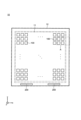
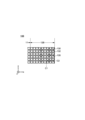
- FIG. 1B is a schematic plan view showing an outline of the configuration of a radio wave reflector 10 according to one embodiment of the present invention.
- the radio wave reflector 10 includes a reflecting antenna area 11 and a peripheral area 12.
- the reflecting antenna area 11 is provided in the center of the radio wave reflector 10, and the peripheral area 12 surrounds the reflecting antenna area 11 and is provided in the peripheral area of the radio wave reflector 10.
- the reflecting antenna area 11 is provided with a plurality of reflecting antenna cells 100.
- the reflecting antenna cells 100 are arranged in a matrix in the x-axis direction and the y-axis direction. However, the arrangement of the reflecting antenna cells 100 is not limited to this.
- the peripheral area is provided with a driving circuit 200 that generates a control signal that controls each of the reflecting antenna cells 100. Wiring is also provided to electrically connect the reflecting antenna cells 100 and the driving circuit 200.
- the peripheral area 12 may be provided with a terminal for supplying a signal or power from the outside.
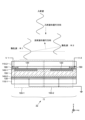
- FIG. 2 is a schematic cross-sectional view showing the configuration of a reflecting antenna cell 100 of a radio wave reflector 10 according to one embodiment of the present invention and the direction in which radio waves are reflected by the reflecting antenna cell 100.
- FIG. 2 shows a first reflecting antenna cell 100-1 and a second reflecting antenna cell 100-2 as two adjacent reflecting antenna cells 100.
- Each of the first reflecting antenna cell 100-1 and the second reflecting antenna cell 100-2 includes a patch electrode 120 provided on the first substrate 110-1 and a ground electrode 130 provided on the second substrate 110-2.
- the patch electrode 120 of the first reflecting antenna cell 100-1 and the patch electrode 120 of the second reflecting antenna cell 100-2 are not electrically connected.
- the ground electrode 130 is provided in common to the first reflecting antenna cell 100-1 and the second reflecting antenna cell 100-2.
- a first alignment film 140-1 is provided on the patch electrode 120.
- a second alignment film 140-2 is provided on the ground electrode 130.
- the first substrate 110-1 and the second substrate 110-2 are arranged so that the patch electrode 120 and the ground electrode 130 face each other, and a liquid crystal layer 150 is provided between the first alignment film 140-1 and the second alignment film 140-2.
- the first substrate 110-1 and the second substrate 110-2 can each be made of glass, quartz, resin, or the like.
- a metallic material can be used for each of the patch electrode 120 and the ground electrode 130.
- the metallic material is molybdenum (Mo), tungsten (W), titanium (Ti), aluminum (Al), copper (Cu), or an alloy of these.
- Mo molybdenum
- tungsten W
- Ti titanium
- Al aluminum
- Cu copper
- Each of the patch electrode 120 and the ground electrode 130 may have a single-layer structure or a multilayer structure.
- the first alignment film 140-1 and the second alignment film 140-2 can each be made of a polyimide resin or the like.
- the first alignment film 140-1 and the second alignment film 140-2 have been subjected to an alignment process using a rubbing method, a photoalignment method, or the like.
- the liquid crystal layer 150 contains a liquid crystal material having dielectric anisotropy.
- the liquid crystal material of the liquid crystal layer 150 may be a nematic liquid crystal or a cholesteric liquid crystal that contains liquid crystal molecules capable of twisted alignment.
- the liquid crystal layer 150 preferably contains a chiral agent to stabilize the twisted alignment of the liquid crystal molecules.
- the initial alignment state (alignment state when no voltage is applied) of the liquid crystal molecules in the liquid crystal layer 150 is controlled by the first alignment film 140-1 and the second alignment film 140-2, which have been subjected to an alignment treatment.
- the alignment state of the liquid crystal molecules in the liquid crystal layer 150 changes, and the dielectric constant of the liquid crystal layer 150 also changes. Details will be described later, but the radio wave reflector 10 uses the change in the dielectric constant of the liquid crystal layer 150 to control the phase of the reflected radio waves.
- the dielectric constant of the liquid crystal is greater when a voltage is applied than when no voltage is applied. Also, when liquid crystal molecules have negative dielectric anisotropy, the dielectric constant of the liquid crystal is smaller when a voltage is applied than when no voltage is applied.
- the liquid crystal layer 150 formed of liquid crystals having dielectric anisotropy can also be considered as a variable dielectric layer. By utilizing the dielectric anisotropy of the liquid crystal layer 150, the reflective antenna cell 100 can control the phase delay (or not delay) of radio waves scattered by the ground electrode 130.
- the frequency bands to which the radio wave reflector 10 is applicable are the very high frequency (VHF) band, the ultra high frequency (UHF) band, the super high frequency (SHF) band, the submillimeter wave (THF: tremendous high frequency) band, and the millimeter wave (EHF: extra high frequency) band.
- VHF very high frequency
- UHF ultra high frequency
- SHF super high frequency
- THF submillimeter wave
- EHF millimeter wave
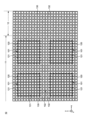
- Fig. 3 is a schematic plan view showing the configuration of the reflecting antenna region 11 and the peripheral region 12 of the radio wave reflector 10 according to one embodiment of the present invention. Specifically, Fig. 3 is a partial enlarged view of the region A including the four reflecting antenna cells 100 in Fig. 1B, and the region A includes a part of the reflecting antenna region 11 and a part of the peripheral region 12.
- the first width w1 and the second width w2 shown in FIG. 4A are spaced apart at equal intervals, but the second width w2 of the fourth opening 134 may vary.
- the fourth opening 134 may be arranged such that the second width w2 gradually decreases in the direction from the reflecting antenna area 11 toward the end face of the radio wave reflector 10A.
- the ground electrodes 133 are densely arranged near the boundary between the two radio wave reflectors 10A, making the boundary between the two radio wave reflectors 10A even less noticeable.
- the ground electrode 133 provided in the peripheral region 12A has been described as having a linear shape, but the planar shape of the ground electrode 133 provided in the peripheral region 12A is not limited to this. Regardless of the shape of the ground electrode 133, the aperture ratio of the peripheral region 12A can be made to approximately match the aperture ratio of the reflecting antenna region by adjusting the size (area, width, etc.) of the ground electrode 133.
- the switching element 160 includes a semiconductor layer 161, a gate insulating layer 162, and a gate electrode 163.
- the semiconductor layer 161 is provided on the first substrate 110-1.
- the gate insulating layer 162 is provided on the first substrate 110-1 so as to cover the semiconductor layer 161.
- the gate electrode 163 is provided on the gate insulating layer 162 so as to overlap with the semiconductor layer 161.
- the gate electrode 163 is electrically connected to the selection signal line 166.
- An interlayer insulating layer 164 is provided on the gate electrode 163.
- the interlayer insulating layer 164 has two openings formed therein through which the semiconductor layer 161 is exposed.
- the semiconductor layer 161 is electrically connected to the patch electrode 120 through one opening, and is electrically connected to the data signal line 167 through the other opening.
- a planarization layer 165 is provided on the interlayer insulating layer 164 and the data signal line 167.
- the patch electrode 120 is provided on the planarization layer 165.
- the data signal line 167 is formed using a metal material such as titanium (Ti), aluminum (Al), or molybdenum (Mo).
- the data signal line 167 is configured with a laminated structure of titanium (Ti)/aluminum (Al)/titanium (Ti), or a laminated structure of molybdenum (Mo)/aluminum (Al)/molybdenum (Mo).
- the planarization layer 165 is formed using a resin material such as acrylic or polyimide.
- the aperture ratio of the reflective antenna region 11 is determined taking into consideration not only the light blocking by the ground electrode 130 but also the light blocking by the switching element 160, the selection signal line 166, and the data signal line 167. That is, in this modification, the aperture ratio of the reflective antenna region 11 is expressed as the total aperture area relative to the area of the reflective antenna region 11.
- the total aperture area is the area of the region in which none of the patch electrode 120, the ground electrode 130, the switching element 160, the selection signal line 166, and the data signal line 167 is provided in a plan view.
- the area of the third opening 132 in the peripheral region 12 may be adjusted so that the aperture ratio of the peripheral region 12 is approximately equal to the aperture ratio of the reflective antenna region 11.
- the radio wave reflecting device 1 is also arranged by combining multiple radio wave reflectors 10B, but the aperture ratio of the peripheral area 12 of the radio wave reflector 10 is approximately the same as the aperture ratio of the reflecting antenna area 11. Therefore, even when two radio wave reflectors 10A are adjacent to each other, the boundary between the two adjacent peripheral areas 12 is not easily noticeable. In other words, in a transparent radio wave reflecting device 1, it is possible to improve visibility at the boundary between the radio wave reflectors 10.
- the radio wave reflecting device 1 is configured by combining and arranging a plurality of radio wave reflecting plates 10B.
- the radio wave reflecting plate 10B includes the same components as the radio wave reflecting plate 10, the description of those components may be omitted.
- FIG. 7 is a schematic plan view showing the configuration of the peripheral region 12B of a radio wave reflector 10B according to one embodiment of the present invention.
- FIG. 8 is a schematic cross-sectional view showing the configuration of the peripheral region 12B of a radio wave reflector 10B according to one embodiment of the present invention. Specifically, FIG. 8 is a cross-sectional view of the peripheral region 12B cut along line C1-C2 in FIG. 7. Note that, for convenience, components on the first substrate 110-1 side and the liquid crystal layer 150 are omitted in FIG. 8.
- the peripheral region 12B of the radio wave reflector 10B includes a ground electrode 130, a third opening 132, multiple dummy pattern electrodes 135, and an insulating layer 136.
- the insulating layer 136 covers the ground electrode 130 and is provided on the ground electrode 130.
- the multiple dummy pattern electrodes 135 are provided on the insulating layer 136. In other words, the multiple dummy pattern electrodes 135 are provided on a different layer from the ground electrode 130.
- the dummy pattern electrode 135 can be made of the same metal material as the ground electrode 130.
- the dummy pattern electrode 135 does not need to be grounded and may be in a floating state.
- the aperture ratio of the peripheral region 12B can be adjusted by adjusting the shape, size, and position of the dummy pattern electrode 135.
- the dummy pattern electrode 135 spaced apart from the ground electrode 130 a configuration similar to the patch electrode 120 spaced apart from the ground electrode 130 in the reflecting antenna region 11 can be formed in the peripheral region 12B. Therefore, the viewing angle dependency of the peripheral region 12B can be made closer to the viewing angle dependency of the reflecting antenna region 11. As a result, even when two radio wave reflectors 10B are adjacent to each other, the boundary between the two adjacent peripheral regions 12B is less noticeable. In other words, in a transparent radio wave reflecting device 1, the visibility of the boundary between the radio wave reflectors 10B can be improved.
Landscapes
- Physics & Mathematics (AREA)
- Electromagnetism (AREA)
- Aerials With Secondary Devices (AREA)
Abstract
電波反射板は、第1の基板の上のパッチ電極と、第1の基板と異なる第2の基板の上の接地電極と、パッチ電極と接地電極との間の液晶層と、平面視において、パッチ電極と接地電極とが重畳する反射アンテナ領域と、平面視において、反射アンテナ領域を囲み、接地電極のみが設けられる周辺領域と、を含み、パッチ電極および接地電極の各々は、複数の開口部を含む。
Description
本発明の一実施形態は、入射する電波の反射方向を制御することのできる電波反射板に関する。また、複数の電波反射板が組み合わせられた電波反射装置に関する。
フェーズドアレイアンテナ(Phased Array Antenna)装置(以下、「電波反射板」という場合がある。)は、面状に配列された複数のアンテナ素子のそれぞれに対し、印加する高周波信号の振幅と位相を調整することでアンテナを固定した状態で指向性を制御している。フェーズドアレイアンテナ装置は移相器を必要とする。液晶の配向状態による誘電率の変化を利用した移相器を用いたフェーズドアレイアンテナ装置が開示されている(例えば、特許文献1参照)。
特許文献1におけるフェーズドアレイアンテナ装置のアンテナ素子は、複数のストリップ配線と、複数のストリップ配線と対向する平面電極と、複数のストリップ配線と平面電極との間に設けられた液晶層と、を有する。複数のアンテナ素子において、複数のストリップ配線に異なる電圧を印加する。そして、アンテナ素子ごとの液晶層の誘電率を調整して、反射波を重ね合わせることで、位相を変化させることができる。これにより、電波の反射方向を任意の方向に設定することができる。
電波反射板は電波基地局を簡素化することができる。但し、電波反射板の設置によって景観が損なわれるという問題があるため、第5世代移動通信システム(G5)用の電波反射板として、透明な電波反射板が要望されている。液晶を用いた電波反射板では、透明化が可能である。また、複数の透明な電波反射板を組み合わせて配置することにより、大面積の透明な電波反射装置を作製することもできる。しかしながら、透明な電波反射装置では、隣接する2つの電波反射板の継ぎ目が目立つなど、電波反射板間の境界における視認性が悪いという問題がある。
本発明の一実施形態は、上記問題に鑑み、複数の電波反射板が組み合わされて配置されたときに、電波反射板間の境界における視認性を向上させる透明な電波反射板を提供することを目的の一つとする。また、本発明の一実施形態は、複数の透明な電波反射板が組み合わされて配置され、電波反射板間の境界における視認性が向上した電波反射装置を提供することを目的の一つとする。
本発明の一実施形態に係る電波反射板は、第1の基板の上のパッチ電極と、第1の基板と異なる第2の基板の上の接地電極と、パッチ電極と接地電極との間の液晶層と、平面視において、パッチ電極と接地電極とが重畳する反射アンテナ領域と、平面視において、反射アンテナ領域を囲み、接地電極のみが設けられる周辺領域と、を含み、パッチ電極および接地電極の各々は、複数の開口部を含む。
第1の電波反射板と、第1の電波反射板と隣接する第2の電波反射板と、を含み、第1の電波反射板および第2の電波反射板の各々は、第1の基板の上のパッチ電極と、第1の基板と異なる第2の基板の上の接地電極と、パッチ電極と接地電極との間の液晶層と、平面視において、パッチ電極と接地電極とが重畳する反射アンテナ領域と、平面視において、反射アンテナ領域を囲み、接地電極のみが設けられる周辺領域と、を含み、パッチ電極および接地電極の各々は、複数の開口部を含み、第1の電波反射板の周辺領域と第2の電波反射板の周辺領域とが接する。
以下、本発明の実施形態を、図面などを参照しながら説明する。但し、本発明は多くの異なる態様で実施することが可能であり、以下に例示する実施形態の記載内容に限定して解釈されるものではない。図面は説明をより明確にするため、実際の態様に比べ、各部の幅、厚さ、形状などについて模式的に表される場合があるが、あくまで一例であって、本発明の解釈を限定するものではない。また、本明細書と図面において、既出の図に関して前述したものと同様の構成要素には、同一の符号を付して、詳細な説明を適宜省略する場合がある。さらに、構成要素に「第1」、「第2」と付記された文字は、構成要素を区別するために用いられる便宜的な標識であり、特段の説明がない限りそれ以上の意味を有しない。
本明細書において、ある部材または領域が他の部材または領域の「上に(または下に)」あるとする場合、特段の限定がない限りこれは他の部材または領域の直上(または直下)にある場合のみでなく他の部材または領域の上方(または下方)にある場合を含み、すなわち、他の部材または領域の上方(または下方)において間に別の構成要素が含まれている場合も含む。
本明細書において、2つの構成要素が「略同一」とは、2つの構成要素の大きさは異なるが形状が同一であること、2つの構成要素の面積の差が±5%以内であること、または2つの構成要素の開口率の差が5%以内であること、を意味する。
図1A~図3を参照して、本発明の一実施形態に係る電波反射装置1または電波反射板10について説明する。
[1.電波反射装置1の構成]
図1Aは、本発明の一実施形態に係る電波反射装置1の構成の概要を示す模式的な平面図である。
図1Aは、本発明の一実施形態に係る電波反射装置1の構成の概要を示す模式的な平面図である。
図1Aに示すように、電波反射装置1は、複数の電波反射板10を含む。2つの電波反射板10は、お互いの端面が接するように配置されている。そのため、1つの電波反射板10は、他の電波反射板10の端面と接する少なくとも1つの端面を含む。図1Aに示す電波反射板10の個数は4個であるが、電波反射装置1における電波反射板10の個数はこれに限られない。電波反射装置1における電波反射板10の個数は、2個以上であればよい。また、図1Aに示す電波反射板10の平面形状は矩形であるが、電波反射装置1における電波反射板10の平面形状はこれに限られない。電波反射装置1における電波反射板10の平面形状は、例えば、六角形であってもよい。なお、電波反射板10は、複数の電波反射板10が組み合わされて配置されたときに、電波反射板10間に間隙を生じない平面形状を有することが好ましい。
[2.電波反射板10の構成]
図1Bは、本発明の一実施形態に係る電波反射板10の構成の概要を示す模式的な平面図である。
図1Bは、本発明の一実施形態に係る電波反射板10の構成の概要を示す模式的な平面図である。
図1Bに示すように、電波反射板10は、反射アンテナ領域11および周辺領域12を含む。反射アンテナ領域11は、電波反射板10の中央部に設けられ、周辺領域12は、反射アンテナ領域11を囲み、電波反射板10の周辺部に設けられている。反射アンテナ領域11には、複数の反射アンテナセル100が設けられている。複数の反射アンテナセル100は、x軸方向およびy軸方向にマトリックス状に配置されている。但し、複数の反射アンテナセル100の配置構成は、この限りではない。周辺領域には、複数の反射アンテナセル100の各々を制御する制御信号を生成する駆動回路200が設けられている。また、反射アンテナセル100と駆動回路200とを電気的に接続するための配線が設けられている。なお、図示しないが、周辺領域12には、外部から信号または電力を供給するための端子が設けられてもよい。
ここで、図2を参照して、反射アンテナセル100の構成および機能について説明する。
図2は、本発明の一実施形態に係る電波反射板10の反射アンテナセル100の構成および反射アンテナセル100による電波の反射方向を示す模式的な断面図である。図2には、隣接する2つの反射アンテナセル100として、第1の反射アンテナセル100-1および第2の反射アンテナセル100-2が示されている。
第1の反射アンテナセル100-1および第2の反射アンテナセル100-2の各々は、第1の基板110-1の上に設けられたパッチ電極120および第2の基板110-2の上に設けられた接地電極130を含む。第1の反射アンテナセル100-1のパッチ電極120と第2の反射アンテナセル100-2のパッチ電極120とは、電気的に接続されていない。一方、接地電極130は、第1の反射アンテナセル100-1および第2の反射アンテナセル100-2に共通して設けられている。パッチ電極120の上には、第1の配向膜140-1が設けられている。接地電極130の上には、第2の配向膜140-2が設けられている。第1の基板110-1と第2の基板110-2とは、パッチ電極120と接地電極130とが対向するように配置され、第1の配向膜140-1と第2の配向膜140-2との間には液晶層150が設けられている。
第1の基板110-1および第2の基板110-2の各々として、ガラス、石英、または樹脂などを用いることができる。
パッチ電極120および接地電極130の各々として、金属材料を用いることができる。例えば、金属材料は、モリブデン(Mo)、タングステン(W)、チタン(Ti)、アルミニウム(Al)、もしくは銅(Cu)またはこれらの合金である。なお、パッチ電極120および接地電極130の各々は、単層構造を有していてもよく、積層構造を有していてもよい。
第1の配向膜140-1および第2の配向膜140-2の各々として、ポリイミド樹脂などを用いることができる。第1の配向膜140-1および第2の配向膜140-2には、ラビング法または光配向法などを用いて配向処理が行われている。
液晶層150は、誘電異方性を有する液晶材料を含む。例えば、液晶層150の液晶材料として、ツイスト配向が可能な液晶分子を含むネマチック液晶またはコレステリック液晶などを用いることができる。また、液晶層150は、液晶分子のツイスト配向を安定化させるため、カイラル剤が含まれていることが好ましい。
配向処理が行われた第1の配向膜140-1および第2の配向膜140-2により、液晶層150内の液晶分子は、初期配向状態(電圧無印加時の配向状態)が制御されている。パッチ電極120に電圧が印加され、パッチ電極120と接地電極130との間に電位差が形成されると、液晶層150内の液晶分子の配向状態が変化し、液晶層150の誘電率も変化する。詳細は後述するが、電波反射板10では、液晶層150の誘電率の変化を利用し、反射する電波の位相を制御する。
液晶分子が正の誘電異方性を有する場合、電圧無印加時よりも電圧印加時の方が、液晶の誘電率が大きくなる。また、液晶分子が負の誘電異方性を有する場合、電圧無印加時よりも電圧印加時の方が、液晶の誘電率が小さくなる。誘電異方性を有する液晶で形成された液晶層150は可変誘電体層とみなすこともできる。反射アンテナセル100は、液晶層150の誘電異方性を利用することで、接地電極130で散乱する電波の位相を遅らせる(または遅らせない)ように制御することができる。
上述したように、第1の反射アンテナセル100-1および第2の反射アンテナセル100-2における基本的な構成は同じである。すなわち、複数の反射アンテナセル100の各々は、上述した基本的な構成を有する。一方、複数の反射アンテナセル100の各々は、スイッチング素子160と電気的に接続されている。具体的には、スイッチング素子160は、パッチ電極120と電気的に接続されており、スイッチング素子160を制御することにより、パッチ電極120に印加される電圧が変化する。
図2に示すように、電波は、第1の基板110-1の表面の法線方向と平行に電波反射板10に入射される(図2中の「入射波の進行方向」参照)。ここで、第1の反射アンテナセル100-1のパッチ電極120には第1の電圧V1が印加され、第2の反射アンテナセル100-2のパッチ電極120には第1の電圧V1と異なる第2の電圧V2が印加されている場合を考える。第1の反射アンテナセル100-1および第2の反射アンテナセル100-2に同じ位相を有する電波が入射すると、第1の反射アンテナセル100-1と第2の反射アンテナセル100-2とでは液晶層150の誘電率が異なることから、第1の反射アンテナセル100-1と第2の反射アンテナセル100-2とにおいて、位相の異なる散乱波が生成される。例えば、図2に示すように、第2の反射アンテナセル100-2で散乱する散乱波R2の位相は、第1の反射アンテナセル100-1で散乱する散乱波R1の位相よりも進む。この場合、反射アンテナ領域11で反射される電波は、第1の基板110-1の表面の法線方向とは異なる方向に進行する(図2中の「反射波の進行方向」参照)。図2には、隣接する2つの反射アンテナセル100を示したが、電波反射板10では、マトリクス状に配置された複数の反射アンテナセル100を別個に制御することができる。そのため、電波反射板10は、電波の反射方向を任意の方向に制御することができる。
電波反射板10の適用対象とする周波数帯は、超短波(VHF:Very High Frequency)帯、極超短波(UHF:Ultra-High Frequency)帯、マイクロ波(SHF:Super High Frequency)帯、サブミリ波(THF:Tremendously high frequency)、ミリ波(EHF:Extra High Frequency)帯である。上述したように、液晶層150では、パッチ電極120に印加される電圧によって液晶分子の配向状態が変化するが、接地電極130に入射する電波の周波数にはほとんど追従しない。液晶分子のこのような特性により、パッチ電極120によって液晶層150の誘電率を変化させつつ、接地電極130で電波を散乱させ、散乱される電波の位相を制御することができる。
[3.反射アンテナ領域11および周辺領域12の構成]
図3は、本発明の一実施形態に係る電波反射板10の反射アンテナ領域11および周辺領域12の構成を示す模式的な平面図である。具体的には、図3は、図1Bにおける4つの反射アンテナセル100を含む領域Aの部分拡大図であり、領域Aは、反射アンテナ領域11の一部および周辺領域12の一部を含む。
図3は、本発明の一実施形態に係る電波反射板10の反射アンテナ領域11および周辺領域12の構成を示す模式的な平面図である。具体的には、図3は、図1Bにおける4つの反射アンテナセル100を含む領域Aの部分拡大図であり、領域Aは、反射アンテナ領域11の一部および周辺領域12の一部を含む。
反射アンテナ領域11において、電波反射板10は、第1の領域101および第2の領域102を含む。第1の領域101は、平面視において、パッチ電極120と接地電極130とが重畳する領域である。すなわち、第1の領域101は、反射アンテナセル100に相当する領域である。第2の領域102は、平面視において、パッチ電極120と接地電極130とが重畳しない領域である。すなわち、第2の領域102は、接地電極130のみが設けられた領域である。
第1の領域101において、パッチ電極120は、複数の第1の開口部121を含む。また、第1の領域101において、接地電極130は、複数の第2の開口部131を含む。第1の開口部121および第2の開口部131の各々の断面形状は矩形であるが、これに限られない。複数の第2の開口部131の平面形状は、複数の第1の開口部121の平面形状と略同一である。第2の開口部131は、第1の開口部121と略同一の開口面積を有し、第1の開口部121と重畳している。そのため、第1の領域101において、光は、第1の開口部121および第2の開口部131を透過することができる。
第2の領域102において、接地電極130は、複数の第3の開口部132を含む。第3の開口部132の断面形状は矩形であるが、これに限られない。複数の第3の開口部132の平面形状は、複数の第2の開口部131の平面形状と略同一である。換言すると、第3の開口部132は、第2の開口部131と略同一の開口面積を有する。第2の領域102ではパッチ電極120が設けられていないため、第2の領域102において、光は、第3の開口部132を透過することができる。
周辺領域12は、第2の領域102と同様の構成を有する。すなわち、周辺領域12において、接地電極130は、複数の第3の開口部132を含む。第2の周辺領域12における接地電極130は、反射アンテナ領域11における接地電極130と略同一の平面形状を有する。具体的には、周辺領域12における接地電極130は、格子形状を有する。周辺領域12ではパッチ電極が設けられていないため、周辺領域12において、光は、第3の開口部132を透過することができる。
パッチ電極120および接地電極130は、光を透過しない。しかしながら、電波反射板10では、光を透過させるために、パッチ電極120および接地電極130に多くの開口部(複数の第1の開口部121、複数の第2の開口部131、および複数の第3の開口部132)が設けられており、電波反射板10に入射した光は、開口部を透過する。そのため、電波反射板10は、透明な電波反射板となる。
電波反射装置1は、複数の電波反射板10が組み合わされて配置されるが、電波反射板10の周辺領域12には、反射アンテナ領域11に設けられている接地電極130と略同一のパターン形状を有する接地電極130が設けられている。そのため、2つの電波反射板10が隣接したときであっても、互いに接する2つの周辺領域12間の境界が目立ちにくい。すなわち、透明性を有する電波反射装置1において、電波反射板10間の境界における視認性を向上させることができる。
<第1実施形態の変形例1>
図4Aおよび図4Bを参照して、電波反射板10の変形例として電波反射板10Aについて説明する。電波反射装置1は、複数の電波反射板10Aを組み合わせて配置する構成も適用することができる。なお、以下では、電波反射板10Aが電波反射板10と同様の構成要素を含むとき、その構成要素の説明を省略する場合がある。
図4Aおよび図4Bを参照して、電波反射板10の変形例として電波反射板10Aについて説明する。電波反射装置1は、複数の電波反射板10Aを組み合わせて配置する構成も適用することができる。なお、以下では、電波反射板10Aが電波反射板10と同様の構成要素を含むとき、その構成要素の説明を省略する場合がある。
図4Aおよび図4Bの各々は、本発明の一実施形態に係る電波反射板10Aの反射アンテナ領域11および周辺領域12Aの構成を示す模式的な平面図である。具体的には、図4Aおよび図4Bの各々は、図1Bにおける4つの反射アンテナセル100を含む領域Aの部分拡大図である。
図4Aに示すように、周辺領域12Aは、接地電極133および複数の第4の開口部134を含む。具体的には、周辺領域12Aには接地電極130と同一の層で形成される接地電極133が設けられ、接地電極133は、y軸方向(すなわち、電波反射板10Aの端面に沿った方向)に延在する複数の第4の開口部134を含む。換言すると、周辺領域12Aには、格子形状を有する接地電極130と異なる直線形状を有する接地電極133が設けられている。接地電極133の直線形状の第1の幅w1は、第4の開口部134の第2の幅w2と同一であってもよく、小さくてもよく、大きくてもよい。第1の幅w1および第2の幅w2は、反射アンテナ領域11の接地電極130の開口率(以下、単に、「反射アンテナ領域11の開口率」という場合がある。)を考慮して決定されてもよい。反射アンテナ領域11の開口率は、反射アンテナ領域11の面積に対する接地電極130の開口面積によって表される。換言すると、反射アンテナ領域11の開口率は、反射アンテナ領域11の面積に対する第2の開口部131および第3の開口部132の合計面積によって表される。一方、周辺領域12の開口率は、周辺領域12の面積に対する接地電極133の開口面積によって表される。換言すると、周辺領域12の開口率は、周辺領域12の面積に対する第4の開口部134の面積によって表される。そのため、例えば、周辺領域12の開口率が反射アンテナ領域11の開口率と略一致するように、第1の幅w1および第2の幅w2を決定してもよい。
なお、周辺領域12Aにおける接地電極133は、反射アンテナ領域11における接地電極130と異なり、ダミーパターンである。そのため、接地電極133は、接地されている必要はなく、フローティング状態であってもよい。
図4Aに示す第1の幅w1および第2の幅w2は、等間隔に設けられていたが、第4の開口部134の第2の幅w2は、変化してもよい。例えば、図4Bに示すように、第4の開口部134は、反射アンテナ領域11から電波反射板10Aの端面に向かう方向において第2の幅w2が徐々に小さくなるように設けられてもよい。この場合、2つの電波反射板10Aの境界付近には、接地電極133が密に配置されることになるため、2つの電波反射板10Aの境界がさらに目立ちにくい。
なお、本変形例では、周辺領域12Aに設けられる接地電極133が直線形状を有するとして説明したが、周辺領域12Aに設けられる接地電極133の平面形状はこれに限られない。接地電極133がどのような形状であっても、接地電極133の大きさ(面積または幅など)を調整することにより、周辺領域12Aの開口率を反射アンテナ領域の開口率に略一致させることができる。
本変形例においても、電波反射装置1は、複数の電波反射板10Aが組み合わされて配置されるが、電波反射板10Aの周辺領域12Aには、周辺領域12Aの開口率が、反射アンテナ領域11の開口率と略同一となるように、接地電極130の平面形状と異なる接地電極133が設けられている。そのため、2つの電波反射板10Aが隣接したときであっても、互いに接する2つの周辺領域12A間の境界が目立ちにくい。すなわち、透明性を有する電波反射装置1において、電波反射板10A間の境界における視認性を向上させることができる。
<第1実施形態の変形例2>
第1の基板110-1上には、パッチ電極120だけでなく、パッチ電極120に供給する電位を制御するためのスイッチング素子が設けられる。ここで、図5および図6を参照して、電波反射板10の反射アンテナ領域11の構成について詳細に説明する。
第1の基板110-1上には、パッチ電極120だけでなく、パッチ電極120に供給する電位を制御するためのスイッチング素子が設けられる。ここで、図5および図6を参照して、電波反射板10の反射アンテナ領域11の構成について詳細に説明する。
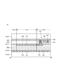
図5は、本発明の一実施形態に係る電波反射板10の反射アンテナ領域11の構成を示す模式的な平面図である。図6は、本発明の一実施形態に係る電波反射板10の反射アンテナ領域11の構成を示す模式的な断面図である。具体的には、図6は、図5中のB1-B2線で切断された反射アンテナ領域11の断面図である。上述したように、第1の領域101は、反射アンテナセル100に相当する。
図5および図6には、スイッチング素子160の一例として、トランジスタが示されている。すなわち、スイッチング素子160は、半導体層161、ゲート絶縁層162、およびゲート電極163を含む。半導体層161は、第1の基板110-1の上に設けられている。ゲート絶縁層162は、半導体層161を覆うように、第1の基板110-1の上に設けられている。ゲート電極163は、半導体層161と重畳するように、ゲート絶縁層162の上に設けられている。ゲート電極163は、選択信号線166と電気的に接続されている。ゲート電極163の上には、層間絶縁層164が設けられている。層間絶縁層164には、半導体層161が露出される2つの開口が形成されている。半導体層161は、一方の開口を介してパッチ電極120と電気的に接続され、他方の開口を介してデータ信号線167と電気的に接続されている。層間絶縁層164およびデータ信号線167の上には、平坦化層165が設けられている。パッチ電極120は、平坦化層165の上に設けられている。
半導体層161は、アモルファスシリコンもしくは多結晶シリコンなどのシリコン半導体、または酸化インジウムガリウム亜鉛、酸化インジウムガリウムアルミニウム、酸化インジウムガリウム、酸化亜鉛、もしくは酸化ガリウムなどの酸化物半導体を用いて形成される。ゲート絶縁層162および層間絶縁層164は、例えば、酸化シリコン膜、または酸化シリコン膜と窒化シリコン膜との積層構造を用いて形成される。ゲート電極163と選択信号線166とは、同一層で形成されていてもよい。ゲート電極163および選択信号線166は、例えば、モリブデン(Mo)、タングステン(W)、またはこれらの合金を用いて形成される。データ信号線167は、チタン(Ti)、アルミニウム(Al)、またはモリブデン(Mo)などの金属材料を用いて形成される。例えば、データ信号線167は、チタン(Ti)/アルミニウム(Al)/チタン(Ti)の積層構造、またはモリブデン(Mo)/アルミニウム(Al)/モリブデン(Mo)の積層構造で構成される。平坦化層165は、アクリルまたはポリイミドなどの樹脂材料を用いて形成される。
選択信号線166およびデータ信号線167は、駆動回路200と電気的に接続されている。駆動回路200からの制御信号は、選択信号線166およびデータ信号線167を介してスイッチング素子160に入力される。スイッチング素子160は、制御信号に基づいて動作し、これにより、液晶層150内の液晶分子の配向状態が変化する。
上述したように、第1の基板110-1上には、パッチ電極120だけでなく、スイッチング素子160が設けられる。スイッチング素子160に含まれる金属材料は、光を透過しない。そこで、本変形例では、反射アンテナ領域11の開口率を、接地電極130による遮光だけでなく、スイッチング素子160、選択信号線166、およびデータ信号線167による遮光も考慮して決定する。すなわち、本変形例では、反射アンテナ領域11の開口率は、反射アンテナ領域11の面積に対する総開口面積で表される。ここで、総開口面積は、平面視において、パッチ電極120、接地電極130、スイッチング素子160、選択信号線166、およびデータ信号線167のいずれもが設けられていない領域の面積である。本変形例では、例えば、周辺領域12の開口率が反射アンテナ領域11の開口率と略一致するように、周辺領域12の第3の開口部132の面積を調整してもよい。
本変形例においても、電波反射装置1は、複数の電波反射板10Bが組み合わされて配置されるが、電波反射板10の周辺領域12の開口率は、反射アンテナ領域11の開口率と略同一である。そのため、2つの電波反射板10Aが隣接したときであっても、互いに接する2つの周辺領域12間の境界が目立ちにくい。すなわち、透明性を有する電波反射装置1において、電波反射板10間の境界における視認性を向上させることができる。
<第2実施形態>
図7および図8を参照して、本発明の一実施形態に係る電波反射装置1および電波反射板10Bについて説明する。電波反射装置1は、複数の電波反射板10Bを組み合わせて配置された構成である。なお、以下では、電波反射板10Bが電波反射板10と同様の構成要素を含むとき、その構成要素の説明を省略する場合がある。
図7および図8を参照して、本発明の一実施形態に係る電波反射装置1および電波反射板10Bについて説明する。電波反射装置1は、複数の電波反射板10Bを組み合わせて配置された構成である。なお、以下では、電波反射板10Bが電波反射板10と同様の構成要素を含むとき、その構成要素の説明を省略する場合がある。
図7は、本発明の一実施形態に係る電波反射板10Bの周辺領域12Bの構成を示す模式的な平面図である。図8は、本発明の一実施形態に係る電波反射板10Bの周辺領域12Bの構成を示す模式的な断面図である。具体的には、図8は、図7中のC1-C2線で切断された周辺領域12Bの断面図である。なお、図8では、便宜上、第1の基板110-1側の構成要素および液晶層150などが省略されている。
図7および図8に示すように、電波反射板10Bの周辺領域12Bは、接地電極130、第3の開口部132、複数のダミーパターン電極135、および絶縁層136を含む。絶縁層136は、接地電極130を覆い、接地電極130の上に設けられている。複数のダミーパターン電極135は、絶縁層136の上に設けられている。すなわち、複数のダミーパターン電極135は、接地電極130と異なる層に設けられている。
ダミーパターン電極135として、接地電極130と同様の金属材料を用いることができる。ダミーパターン電極135は、接地されている必要はなく、フローティング状態であってもよい。
図7に示すダミーパターン電極135の平面形状は矩形であるが、ダミーパターン電極135の平面形状はこれに限られない。ダミーパターン電極135の平面形状は、円形であってもよい。また、ダミーパターン電極135の大きさは、特に限定されない。例えば、ダミーパターン電極135の面積は、第3の開口部132の開口面積と同じであってもよく、大きくてもよく、小さくてもよい。さらに、ダミーパターン電極135が配置される位置も、特に限定されない。ダミーパターン電極135は、接地電極130と重畳するように配置されていてもよく、接地電極130と重畳しないように配置されていてもよい。
本実施形態では、ダミーパターン電極135の形状、大きさ、および位置を調整することにより、周辺領域12Bの開口率を調整することができる。また、接地電極130と離間したダミーパターン電極135を設けることにより、反射アンテナ領域11内の接地電極130と離間したパッチ電極120と同様の構成を周辺領域12Bに形成することができる。そのため、周辺領域12Bの視野角依存性を、反射アンテナ領域11の視野角依存性に近づけることができる。これにより、2つの電波反射板10Bが隣接したときであっても、互いに接する2つの周辺領域12B間の境界が目立ちにくい。すなわち、透明性を有する電波反射装置1において、電波反射板10B間の境界における視認性を向上させることができる。
なお、上述では、第2の基板110-2上にダミーパターン電極135を設ける構成を説明したが、本実施形態では、ダミーパターン電極135を第1の基板110-1上に設ける構成も適用することができる。
本発明の実施形態および変形例は、相互に矛盾しない限りにおいて、適宜組み合わせて実施することができる。また、実施形態を基にして、当業者が適宜構成要素の追加、削除、もしくは設計変更を行ったもの、または、工程の追加、省略、もしくは条件変更を行ったものも、本発明の要旨を備えている限り、本発明の範囲に含まれる。
上述した実施形態によりもたらされる作用効果とは異なる他の作用効果であっても、本明細書の記載から明らかなもの、または、当業者において容易に予測し得るものについては、当然に本発明によりもたらされるものと解される。
1:電波反射装置、 10、10A、10B:電波反射板、 11:反射アンテナ領域、 12、12A、12B:周辺領域、 100:反射アンテナセル、 100-1:第1の反射アンテナセル、 100-2:第2の反射アンテナセル、 101:第1の領域、 102:第2の領域、 110-1:第1の基板、 110-2:第2の基板、 120:パッチ電極、 121:第1の開口部、 130、133:接地電極、 131:第2の開口部、 132:第3の開口部、 134:第4の開口部、 135:ダミーパターン電極、 136:絶縁層、 140-1:第1の配向膜、 140-2:第2の配向膜、 150:液晶層、 160:スイッチング素子、 161:半導体層、 162:ゲート絶縁層、 163:ゲート電極、 164:層間絶縁層、 165:平坦化層、 166:選択信号線、 167:データ信号線、 200:駆動回路
Claims (12)
- 第1の基板の上のパッチ電極と、
前記第1の基板と異なる第2の基板の上の接地電極と、
前記パッチ電極と前記接地電極との間の液晶層と、
平面視において、前記パッチ電極と前記接地電極とが重畳する反射アンテナ領域と、
前記平面視において、前記反射アンテナ領域を囲み、前記接地電極のみが設けられる周辺領域と、を含み、
前記パッチ電極および前記接地電極の各々は、複数の開口部を含む、電波反射板。 - 前記周辺領域内の前記接地電極の前記複数の開口部は、前記反射アンテナ領域内の前記接地電極の前記複数の開口部と略同一の平面形状を有する、請求項1に記載の電波反射板。
- 前記周辺領域の開口率は、前記反射アンテナ領域の開口率と略同一である、請求項1に記載の電波反射板。
- 前記周辺領域内の前記接地電極は、格子形状を有する、請求項1に記載の電波反射板。
- 前記周辺領域内の前記接地電極は、直線形状を有する、請求項1に記載の電波反射板。
- 前記周辺領域において、前記接地電極と異なる層として、ダミーパターン電極が設けられる、請求項1に記載の電波反射板。
- 第1の電波反射板と、
前記第1の電波反射板と隣接する第2の電波反射板と、を含み、
前記第1の電波反射板および前記第2の電波反射板の各々は、
第1の基板の上のパッチ電極と、
前記第1の基板と異なる第2の基板の上の接地電極と、
前記パッチ電極と前記接地電極との間の液晶層と、
平面視において、前記パッチ電極と前記接地電極とが重畳する反射アンテナ領域と、
前記平面視において、前記反射アンテナ領域を囲み、前記接地電極のみが設けられる周辺領域と、を含み、
前記パッチ電極および前記接地電極の各々は、複数の開口部を含み、
前記第1の電波反射板の前記周辺領域と前記第2の電波反射板の前記周辺領域とが接する、電波反射装置。 - 前記第1の電波反射板および前記第2の電波反射板の各々において、前記周辺領域内の前記接地電極の前記複数の開口部は、前記反射アンテナ領域内の前記接地電極の前記複数の開口部と略同一の平面形状を有する、請求項7に記載の電波反射装置。
- 前記第1の電波反射板および前記第2の電波反射板の各々において、前記周辺領域の開口率は、前記反射アンテナ領域の開口率と略同一である、請求項7に記載の電波反射装置。
- 前記第1の電波反射板および前記第2の電波反射板の各々において、前記周辺領域内の前記接地電極は、格子形状を有する、請求項7に記載の電波反射装置。
- 前記第1の電波反射板および前記第2の電波反射板の各々において、前記周辺領域内の前記接地電極は、直線形状を有する、請求項7に記載の電波反射装置。
- 前記第1の電波反射板および前記第2の電波反射板の各々の前記周辺領域において、前記接地電極と異なる層として、ダミーパターン電極が設けられる、請求項7に記載の電波反射装置。
Applications Claiming Priority (2)
| Application Number | Priority Date | Filing Date | Title |
|---|---|---|---|
| JP2023-223124 | 2023-12-28 | ||
| JP2023223124 | 2023-12-28 |
Publications (1)
| Publication Number | Publication Date |
|---|---|
| WO2025142111A1 true WO2025142111A1 (ja) | 2025-07-03 |
Family
ID=96218919
Family Applications (1)
| Application Number | Title | Priority Date | Filing Date |
|---|---|---|---|
| PCT/JP2024/038699 Pending WO2025142111A1 (ja) | 2023-12-28 | 2024-10-30 | 電波反射板および電波反射装置 |
Country Status (1)
| Country | Link |
|---|---|
| WO (1) | WO2025142111A1 (ja) |
Citations (3)
| Publication number | Priority date | Publication date | Assignee | Title |
|---|---|---|---|---|
| JP2012249204A (ja) * | 2011-05-30 | 2012-12-13 | Kobe Steel Ltd | マイクロ波平面アンテナ |
| WO2020095786A1 (ja) * | 2018-11-06 | 2020-05-14 | Agc株式会社 | 基板 |
| WO2023095566A1 (ja) * | 2021-11-25 | 2023-06-01 | 株式会社ジャパンディスプレイ | 電波反射板 |
-
2024
- 2024-10-30 WO PCT/JP2024/038699 patent/WO2025142111A1/ja active Pending
Patent Citations (3)
| Publication number | Priority date | Publication date | Assignee | Title |
|---|---|---|---|---|
| JP2012249204A (ja) * | 2011-05-30 | 2012-12-13 | Kobe Steel Ltd | マイクロ波平面アンテナ |
| WO2020095786A1 (ja) * | 2018-11-06 | 2020-05-14 | Agc株式会社 | 基板 |
| WO2023095566A1 (ja) * | 2021-11-25 | 2023-06-01 | 株式会社ジャパンディスプレイ | 電波反射板 |
Similar Documents
| Publication | Publication Date | Title |
|---|---|---|
| US12117698B2 (en) | Intelligent reflecting surface and intelligent reflecting device | |
| US20250015508A1 (en) | Reflect array | |
| US20250149800A1 (en) | Reflecting device | |
| US20240243484A1 (en) | Reflect array | |
| US20240364008A1 (en) | Reflect array | |
| US20260074434A1 (en) | Reflecting device | |
| WO2025142111A1 (ja) | 電波反射板および電波反射装置 | |
| WO2025142110A1 (ja) | 電波反射板 | |
| WO2025142109A1 (ja) | 電波反射板 | |
| WO2024116573A1 (ja) | 電波反射装置 | |
| US20250266865A1 (en) | Intelligent reflecting surface | |
| US20250226588A1 (en) | Intelligent reflecting surface | |
| US20250389989A1 (en) | Intelligent reflecting surface | |
| US20250379367A1 (en) | Intelligent reflecting surface | |
| US12578599B2 (en) | Reflecting device having liquid crystal material | |
| US20250379366A1 (en) | Intelligent reflecting surface and reflecting device | |
| US20250379617A1 (en) | Intelligent reflecting surface | |
| US20260005436A1 (en) | Reflecting element for intelligent reflecting surface | |
| US20260011928A1 (en) | Intelligent reflecting surface | |
| US20260024919A1 (en) | Intelligent reflecting surface | |
| US20260003234A1 (en) | Intelligent reflecting surface | |
| WO2026088586A1 (ja) | 電波反射装置 | |
| CN120266344A (zh) | 电波反射装置 | |
| WO2025027981A1 (ja) | 電波反射装置の検査装置、およびその検査方法 | |
| KR20250091286A (ko) | 전파 반사 장치 |
Legal Events
| Date | Code | Title | Description |
|---|---|---|---|
| 121 | Ep: the epo has been informed by wipo that ep was designated in this application |
Ref document number: 24912004 Country of ref document: EP Kind code of ref document: A1 |