WO2025123003A1 - Advanced sampling methods for faster molecular sensor response to highly dilute analytes - Google Patents
Advanced sampling methods for faster molecular sensor response to highly dilute analytes Download PDFInfo
- Publication number
- WO2025123003A1 WO2025123003A1 PCT/US2024/059139 US2024059139W WO2025123003A1 WO 2025123003 A1 WO2025123003 A1 WO 2025123003A1 US 2024059139 W US2024059139 W US 2024059139W WO 2025123003 A1 WO2025123003 A1 WO 2025123003A1
- Authority
- WO
- WIPO (PCT)
- Prior art keywords
- waveform
- analyte
- sensor
- aptamer
- binding affinity
- Prior art date
- Legal status (The legal status is an assumption and is not a legal conclusion. Google has not performed a legal analysis and makes no representation as to the accuracy of the status listed.)
- Pending
Links
Classifications
-
- G—PHYSICS
- G01—MEASURING; TESTING
- G01N—INVESTIGATING OR ANALYSING MATERIALS BY DETERMINING THEIR CHEMICAL OR PHYSICAL PROPERTIES
- G01N33/00—Investigating or analysing materials by specific methods not covered by groups G01N1/00 - G01N31/00
- G01N33/48—Biological material, e.g. blood, urine; Haemocytometers
- G01N33/50—Chemical analysis of biological material, e.g. blood, urine; Testing involving biospecific ligand binding methods; Immunological testing
- G01N33/53—Immunoassay; Biospecific binding assay; Materials therefor
- G01N33/5308—Immunoassay; Biospecific binding assay; Materials therefor for analytes not provided for elsewhere, e.g. nucleic acids, uric acid, worms, mites
-
- A—HUMAN NECESSITIES
- A61—MEDICAL OR VETERINARY SCIENCE; HYGIENE
- A61B—DIAGNOSIS; SURGERY; IDENTIFICATION
- A61B5/00—Measuring for diagnostic purposes; Identification of persons
- A61B5/145—Measuring characteristics of blood in vivo, e.g. gas concentration or pH-value ; Measuring characteristics of body fluids or tissues, e.g. interstitial fluid or cerebral tissue
-
- A—HUMAN NECESSITIES
- A61—MEDICAL OR VETERINARY SCIENCE; HYGIENE
- A61B—DIAGNOSIS; SURGERY; IDENTIFICATION
- A61B5/00—Measuring for diagnostic purposes; Identification of persons
- A61B5/68—Arrangements of detecting, measuring or recording means, e.g. sensors, in relation to patient
- A61B5/6846—Arrangements of detecting, measuring or recording means, e.g. sensors, in relation to patient specially adapted to be brought in contact with an internal body part, i.e. invasive
- A61B5/6847—Arrangements of detecting, measuring or recording means, e.g. sensors, in relation to patient specially adapted to be brought in contact with an internal body part, i.e. invasive mounted on an invasive device
- A61B5/685—Microneedles
-
- G—PHYSICS
- G01—MEASURING; TESTING
- G01N—INVESTIGATING OR ANALYSING MATERIALS BY DETERMINING THEIR CHEMICAL OR PHYSICAL PROPERTIES
- G01N27/00—Investigating or analysing materials by the use of electric, electrochemical, or magnetic means
- G01N27/26—Investigating or analysing materials by the use of electric, electrochemical, or magnetic means by investigating electrochemical variables; by using electrolysis or electrophoresis
- G01N27/28—Electrolytic cell components
- G01N27/30—Electrodes, e.g. test electrodes; Half-cells
- G01N27/327—Biochemical electrodes, e.g. electrical or mechanical details for in vitro measurements
- G01N27/3275—Sensing specific biomolecules, e.g. nucleic acid strands, based on an electrode surface reaction
- G01N27/3276—Sensing specific biomolecules, e.g. nucleic acid strands, based on an electrode surface reaction being a hybridisation with immobilised receptors
-
- A—HUMAN NECESSITIES
- A61—MEDICAL OR VETERINARY SCIENCE; HYGIENE
- A61B—DIAGNOSIS; SURGERY; IDENTIFICATION
- A61B5/00—Measuring for diagnostic purposes; Identification of persons
- A61B5/0002—Remote monitoring of patients using telemetry, e.g. transmission of vital signals via a communication network
-
- C—CHEMISTRY; METALLURGY
- C12—BIOCHEMISTRY; BEER; SPIRITS; WINE; VINEGAR; MICROBIOLOGY; ENZYMOLOGY; MUTATION OR GENETIC ENGINEERING
- C12N—MICROORGANISMS OR ENZYMES; COMPOSITIONS THEREOF; PROPAGATING, PRESERVING, OR MAINTAINING MICROORGANISMS; MUTATION OR GENETIC ENGINEERING; CULTURE MEDIA
- C12N2310/00—Structure or type of the nucleic acid
- C12N2310/10—Type of nucleic acid
- C12N2310/16—Aptamers
Definitions
- Electrochemical aptamer sensors can identify the presence and/or concentration of an analyte of interest via the use of an aptamer sequence that specifically binds to the analyte of interest.
- These sensors may include aptamers attached to an electrode, wherein each of the aptamers has a redox active molecule (redox tag) attached thereto.
- the redox couple can transfer electrical charge to or from the electrode.
- an analyte binds to the aptamer
- the aptamer changes shape, bringing the redox couple closer to or further from, on average, the electrode. This results in a measurable change in electrical current that can be translated to a measure of presence or concentration of the analyte.
- aptamer sensors are an example of an affinity-based biosensor. Other aptamer switching and measurement modes can also result in a measurable change in redox electrical current.
- a major unresolved challenge for current aptamer sensors and other affinity-based biosensors is a limit on the range of detection that can be achieved by the sensors when testing for the presence or concentration of highly dilute analytes – such as in the nanomolar (nM) or picomolar (pM) ranges (or even lower ranges of concentration).
- highly dilute analytes — such as in the nanomolar (nM) or picomolar (pM) ranges (or even lower ranges of concentration.
- nM nanomolar
- pM picomolar
- a sensor for insulin which has concentrations of analyte in 10’s to 100’s of pM in blood and in interstitial fluid, may not be able to measure accurately a decrease in insulin in the body because while insulin in the body may decrease in less than an hour, it could require greater than 10 hours for the insulin sensor to release the insulin from the aptamers and properly report a measurement of insulin that correlates with concentrations in the body.
- Another major unresolved challenge is that the electrical measurement technique used with aptamer sensors can also significantly alter the binding affinity by making the binding affinity weaker. [0006] And so, a need still exists for devices and methods to enable faster aptamer sensors responses to highly dilute analytes.
- One aspect of the present invention is directed to a method for continually sensing at least one analyte.
- the method includes bringing a sample including at least one analyte into contact with at least one sensor having an electrode and a plurality of aptamers that are capable of binding to the analyte.
- At least some of the aptamers each carry at least one tag (such as a redox tag), wherein each tag changes in at least one parameter when analyte binds to its associated aptamer (such as by being brought closer to or further from, on average, the electrode (which results in a measurable change in electrical current that can be translated to a measure of presence or concentration of the analyte).
- the method also includes applying a first electronic waveform to the at least one sensor, wherein the first electronic waveform is associated with a first binding affinity between the analyte and the plurality of aptamers.
- the method also includes applying a second electronic waveform to the at least one sensor, wherein the second electronic waveform is associated with a second binding affinity between the analyte and the plurality of aptamers.
- the first electronic waveform and second electronic waveform are different waveforms, and the first binding affinity and second binding affinity differ by at least 2X.
- the method may further include detecting the presence of analyte or measuring the concentration of analyte: (a) during and/or after applying the first electronic waveform, (b) during and/or after applying the second electronic waveform, or (c) during and/or after applying the first electronic waveform and during and/or after applying the second electronic waveform.
- FIG. 1 is a schematic of an embodiment of a sensor device including a plurality of microneedles.
- FIG. 1 is a schematic of an embodiment of a sensor device including a plurality of microneedles.
- FIG. 2 is a schematic of another embodiment of a sensor device including a single microneedle or needle or strip.
- FIG.3 is a schematic showing a working electrode for a sensor device having a plurality of aptamers bound thereto, and illustrating examples of aptamer conformations with and without analyte bound to the aptamer.
- FIG. 4 is a diagram of an example environment in which systems and/or methods described herein may be implemented.
- FIG. 5 is a schematic showing an example wearable monitoring device according to the present invention.
- FIG. 6 is a plot of binding affinity (Kd) vs. time (min) for an analyte and aptamer in accordance with principles of the present invention.
- FIG.7 is another plot of binding affinity (Kd) vs. time (min) for an analyte and aptamer in accordance with principles of the present invention.
- FIG. 8 is a plot of actual and measured concentrations vs. time for two different electronic sampling methods in accordance with principles of the present invention.
- FIG. 9 is a plot of sensor response in terms of redox current vs. analyte concentration for two different electronic sampling methods in accordance with principles of the present invention.
- FIG. 10A is a graph demonstrating electrical measurement techniques using square wave voltammetry.
- FIG.10B is a graph showing “forward,” “backward,” and “net” voltammograms.
- FIG. 11 is a graph showing in vivo data collected for a cortisol sensor inserted subcutaneously in a rat, showing sensor response versus time following injection of the cortisol analyte.
- FIG.12 is a graph of the cumulative distribution function (CDF) versus lower limit of quantification (LLOQ) for SomaLogic aptamers (commercially available from SomaLogic Operating Co., Inc., Boulder, CO).
- CDF cumulative distribution function
- LLOQ lower limit of quantification
- analyte sensor or “continuous sensing” or “continuous monitoring” with a “continuous sensor” or “continuous analyte sensor” or “continuous monitor,” or “continual sensing” or “continual monitoring” with a “continual sensor” or “continual analyte sensor” or “continual monitor” means a sensor, monitor, sensing, or monitoring that provides a measurement that responds to changing concentration of at least one analyte in a solution, and which includes the capability of a device to provide multiple measurements of an analyte over time.
- Such sensors can include electrochemical sensors such as those using aptamers for affinity based sensing or other suitable measures, may include mechanical or optical sensors, such as those based on biolayer interferometry, or other sensing mechanisms that support one or more embodiments of the present invention.
- analyte means any solute in a solution or fluid which can be measured using a sensor. Analytes can be small molecules, proteins, peptides, electrolytes, acids, bases, antibodies, molecules with small molecules bound to them, DNA, RNA, drugs, chemicals, pollutants, or other solutes in a solution or fluid.
- electrode means any material that is electrically conductive such as gold, platinum, nickel, silicon, conductive liquid infused materials such as ionic liquids, PEDOT:PSS, conductive oxides, carbon, boron-doped diamond, nanotubes or nanowire meshes, or other suitable electrically conducting materials.
- working electrode means the electrode that is performing the sensing, such as the electrode that carries sensing chemistry such as aptamers. Counter and reference electrodes or just counter electrodes are further required for operation in a 3 or 2 electrode electrochemical measurement system, respectively. A working electrode may also be referred to as “a sensor” or “the sensor”.
- support or “sensor support” means at least one material that allows placement of the sensor into skin and which is able to maintain position of the sensor in skin.
- the support may be an insulating material such as a plastic or ceramic, or for example may be an electrode such as a gold, tantalum, tungsten, or other type of wire. In some cases, the support may also be an electrode required for operation of the sensor.
- the term “about,” when referring to a value or to an amount of mass, weight, time, volume, pH, size, concentration or percentage is meant to encompass variations of ⁇ 20% in some embodiments, ⁇ 10% in some embodiments, ⁇ 5% in some embodiments, ⁇ 1% in some embodiments, ⁇ 0.5% in some embodiments, and ⁇ 0.1% in some embodiments from the specified amount, as such variations are appropriate to perform the disclosed method.
- the term “protective layer” means a homogeneous or heterogeneous layer of material or of one or more types of molecules on an electrode which reduce electrochemical background current and/or current due to electrochemical interference, and which may promote proper freedom of movement for the aptamer which is required for creating a measurable response to analyte concentration.
- the term “antifouling layer” means a homogeneous or heterogeneous layer of material or of one or more types of molecules on a surface which reduces fouling on a surface compared to if such an antifouling layer was not utilized. A protective layer may also act as an antifouling layer.
- a permi-selective membrane such as polybetaine may also be an anti- fouling layer.
- aptamer means a molecule that undergoes a conformation or binding change as an analyte binds to the molecule, and which satisfies the general operating principles of the sensing method as described herein.
- Such molecules are, e.g., natural or modified DNA, RNA, or XNA oligonucleotide sequences, spiegelmers, peptide aptamers, and affimers.
- Modifications may include substituting unnatural nucleic acid bases for natural bases within the aptamer sequence, replacing natural sequences with unnatural sequences, or other suitable modifications that improve sensor function, but which behave analogous to traditional aptamers.
- Two or more aptamers bound together can also be referred to as an aptamer (i.e., not separated in solution).
- Aptamers can have molecular weights of at least 1 kDa, 10 kDa, or 100 kDa.
- the term “redox tag” or “redox molecule” means any species such as small or large molecules with a redox active portion that when brought adjacent to an electrode can reversibly transfer at least one electron with the electrode.
- Redox tag or molecule examples include methylene blue, ferrocene, quinones, or other suitable species that satisfy the definition of a redox tag or molecule.
- a redox tag or molecule is referred to as a redox mediator.
- Redox tags or molecules may also exchange electrons or change in behavior when brought into proximity with other redox tags or molecules. Exogenous redox molecules are those added to a device, e.g. they are not endogenous and provided by the sample fluid to be tested.
- the term “change in electron transfer” means a redox molecule whose electron transfer with an electrode has changed in a measurable manner.
- This change in electron transfer can, for example, originate from availability for electron transfer, distance from an electrode, diffusion rate to or from an electrode, a shift or increase or decrease in electrochemical activity of the redox molecule, or any other embodiment as taught herein that results in a measurable change in electron transfer between the redox molecule and the electrode.
- sensing monolayer means at least a plurality of aptamers on a working electrode, which may also include a plurality of molecules or mixtures of molecules that form a protective layer and/or an anti-fouling layer.
- a “device” comprises at least one sensor based on at least one aptamer and at least one sensor solution. Devices can sense multiple samples and be in multiple configurations such as a microneedle or in-dwelling sensor needle to measure interstitial fluid, or an implanted device.
- sensor off times, sensor response times, lag times, and analyte-aptamer dissociation times means a time period after a change in analyte concentration that is reproducible across multiple measurements such as a 90% to 10% response time, or 10% binding to 90% binding.
- sensor off times, sensor response times, lag times, and analyte-aptamer dissociation times means a time period after a change in analyte concentration that is reproducible across multiple measurements such as a 90% to 10% response time, or 10% binding to 90% binding.
- oscillating voltammetry includes any electrochemical measurement waveform with waveforms that oscillate both positive and negative in potential multiple times (at least more than twice) capturing both oxidation and reduction currents of a redox tag on an aptamer in a period less than 500 ms.
- oscillating voltammetry may include but is not limited to square wave voltammetry, differential pulse voltammetry, and alternating current voltammetry are all examples of “oscillating voltammetry” as taught in “Comparison of voltammetric methods used in the interrogation of electrochemical aptamer-based sensors” DOI: 10.1039/D3SD00083D, Sens.
- Certain embodiments of the disclosed invention show sensors as simple individual elements. It is understood that many sensors require two or more electrodes, reference electrodes, or additional supporting technology or features which are not captured in the description herein. Sensors can be in duplicate, triplicate, or more, to provide improved data and readings. Sensors may provide continual, continuous, or discrete data and/or readings.
- Certain embodiments of the disclosed invention show sub-components of what would be sensing devices with more sub- components needed for use of the device in various applications, which are known (e.g., a reference or counter electrode, a battery, antenna, adhesive), and for purposes of brevity and focus on inventive aspects, such components may not be explicitly shown in the diagrams or described in the embodiments of the disclosed invention. All ranges of parameters disclosed herein include the endpoints of the ranges. [0041] With reference to FIG. 1, one embodiment of a sensor device 100 is shown.
- the illustrated embodiment of the sensor device 100 includes: a microneedle support 110 that can be made of metal, semiconductor, or plastic for example, and at least one working electrode 120 such as gold, carbon, platinum, or other suitable electrode material.
- Counter and references electrodes are not shown and may be included on support 110.
- the device may also comprise electronics (not shown) for reading the sensor 120 and communicating data to a user or smart phone (not shown).
- Electrode 120 may also be a component of an aptamer sensor.
- An example of such an aptamer sensor including the working electrode 120 may include at least one blocking layer of a plurality of molecules such as mercaptohexanol (which may be thiol bonded to the electrode 120), and at least one aptamer that is responsive to binding to an analyte and which is associated with a redox tag such as methylene blue.
- this embodiment of device 100 by be introduced to a sample fluid, such as dermal interstitial fluid of skin 12 is shown.
- the working electrode(s) 120 are typically for the same analyte, such as cortisol for example, and are shown as embedded through the epidermis 12a and into the dermis 12b.
- the working electrodes may potentially be embedded into the hypodermis 12c.
- the depth of penetration into skin 12 by the device 100 is typically 100’s of ⁇ m (often 500-700 ⁇ m) for microneedle arrays as shown in FIG.1.
- the device 100 may also use hollow microneedles and a sensor which is inside the hollow microneedles [or which is outside the body (not shown)], as taught by, Friedel M, Werbovetz B, Drexelius A, Watkins Z, Bali A, Plaxco KW, Heikenfeld J. Continuous molecular monitoring of human dermal interstitial fluid with microneedle-enabled electrochemical aptamer sensors. Lab Chip.2023 Jul 12;23(14):3289- 3299. doi: 10.1039/d3lc00210a.
- each illustrated microneedle on support 110 includes a working electrode 120 disposed inside the microneedle and positioned at the open end of each needle.
- each of these electrodes may be part of an aptamer sensor, and thus have at least one aptamer associated therewith [such as by being bound to a surface of the electrode(s) 120].
- a conventional prior art sensor device 200 is shown. This device 200 includes a single needle element with a working electrode 220 embedded in the hypodermis 12c (shown) or dermis 12b (not shown). This arrangement is commonly employed in continuous glucose monitors.
- the working electrode 220 is embedded deeply enough with adequate penetrating depth (e.g. ⁇ 5 mm) such that for most users of the device 200 the working electrode 220 will always be securely in the hypodermis 12c during use of the device 200.
- the prior art has at least one approach where the working electrode depth of penetration into tissue is predetermined.
- FIGS. 1 and 2 are wearable examples of sensors, sensors of the present invention may also be fully implanted into the body (not shown).
- other embodiments of a device in accordance with aspects of the present invention by not be embedded in microneedles, or include microneedles at all – but may be a device to which a collected sample is introduced outside the body of a subject.
- an aptamer sensor that includes at least one or more aptamers associated with the working electrode.
- the working electrode 320 is comprised of an electrode material such as gold.
- the gold is then incubated with aptamers 350 via thiol attachment to the electrode 320, and the aptamer 350 includes a redox tag 352, such as methylene blue.
- the electrode surface is further incubated with a protective monolayer 356 such as mercaptohexanol, mercaptoocotanol, or other suitable chemistry.
- a protective membrane such as polybetaine hydrogel or other suitable material may be added to prevent fouling of the monolayer surface.
- the working electrode 320 may be preserved in a preservative such as trehalose to enable dry storage.
- the aptamer sensor shown in FIG.3 is brought into contact with a sample from a subject (a sample to be tested for the presence and/or concentration of a particular analyte or analytes).
- the aptamer, as described above, is a molecule that has a binding affinity for the target analyte.
- binding of aptamer 350 to analyte 354 causes a shape conformation change which brings the redox tag 352 closer to the electrode 320 resulting in increased electron transfer (increased electrical current).
- aptamer at the right side of figure is not bound to analyte, whereas aptamer at the left side of the figure has bound analyte and, as a result, redox tag 352 is brought closer to surface of electrode 320.
- concentration of analyte 354 increases, more binding of analyte 354 to aptamers 350 occurs (as there will typically be a plurality of such aptamers with associated redox tags present on surface of electrode 320), and more electron transfer occurs (more measurable electrical current).
- concentration of analyte 354 decreases, conversely electrical current decreases.
- FIG. 4 illustrates a diagram of an example environment 800 in which systems and/or methods described herein may be implemented.
- Reference numerals for aspects or features shown in FIG. 4 do not necessarily correspond to reference numerals of similar or corresponding aspects or features shown in other figures. As shown in FIG.
- example environment 800 may include a plurality of sensor devices (designated generally by reference number 802) and a plurality of user devices (designated generally by the reference 804) that are linked together by one or more network(s) (designated generally by the reference 806).
- the network(s) 806 provide(s) communications links between the various sensor devices 802 and/or user devices 804 and may be supported by networking components 807 that interconnect the sensor devices 802 and/or user devices 804, including for example, routers, hubs, firewalls, network interfaces, wired or wireless communications links and corresponding interconnections, cellular stations and corresponding cellular conversion technologies (e.g., to convert between cellular and Transmission Control Protocol (TCP) / Internet Protocol (IP), etc.).
- TCP Transmission Control Protocol
- IP Internet Protocol
- the network(s) 806 may comprise connections using one or more intranets, extranets, local area networks (LANs), wide area networks (WANs), Wi-Fi networks, the Internet, including the world wide web, cellular and/or other arrangements for enabling communication between the sensor devices 802 and/or the user devices 804, in either real time or otherwise (e.g., via time shifting, batch processing, etc.), and/or any other connections known in the art.
- LANs local area networks
- WANs wide area networks
- Wi-Fi networks the Internet, including the world wide web
- the Internet including the world wide web
- Sensor device 802 includes one or more devices capable of receiving, measuring, detecting, storing, processing, and/or transmitting information associated with the presence and/or concentration of a target analyte in a sample fluid (such as, for example, a change in electrical current between redox tag and electrode of aptamer sensor devices).
- sensor device 802 may include a wearable monitoring device (e.g., a purpose-driven appliance, an Internet of Things (IoT) device, a special purpose device, etc.), a device configured with one or more electrodes, a device capable of detecting analyte material such as aptamers, and/or a similar type of device.
- a sensor device 802 implemented as a wearable monitoring device is schematically illustrated in FIG.
- the wearable monitoring device can attach to other parts of a patient’s body.
- the sensor device 802 may be a monitoring device that is not worn by a patient.
- the sensor device 802 e.g., the wearable monitoring device
- can communicate locally e.g., to a user device 804) via Bluetooth, ultrawide band, via one or more radio frequencies (RF) or via any other form of wired or wireless communication.
- RF radio frequencies
- sensor device 802 (e.g., the wearable monitoring device) can communicate across a network, e.g., via Wi-Fi and/or communicate locally to another sensor device 802 and/or to a user device 804.
- User device 804 includes one or more devices capable of receiving, storing, processing, and/or providing information associated with the presence and/or concentration of a target analyte in a sample fluid (such as, for example, a change in electrical current between redox tag and electrode of aptamer sensor devices).
- user device 804 may include a device, such as a tablet computer (e.g., an iPad, etc.), a mobile phone (e.g., a smart phone, a radiotelephone, etc.), a laptop computer, a handheld computer, a server computer, an edge device, a gaming device, a wearable communication device (e.g., a smart wristwatch, a pair of smart eyeglasses, etc.), or a similar type of device.
- a tablet computer e.g., an iPad, etc.
- a mobile phone e.g., a smart phone, a radiotelephone, etc.
- laptop computer e.g., a laptop computer, a handheld computer, a server computer, an edge device, a gaming device, a wearable communication device (e.g., a smart wristwatch, a pair of smart eyeglasses, etc.), or a similar type of device.
- a wearable communication device e.g., a smart wristwatch, a pair of
- user device 804 may be any device capable of communicating with another user device 804 and/or with a sensor device 802, e.g., via Bluetooth, Ultrawide band, near field communication (NFC), via one or more radio frequencies (RF) or via any other form of wired or wireless communication, over the network 806, or any combination thereof.
- a sensor device 802 e.g., via Bluetooth, Ultrawide band, near field communication (NFC), via one or more radio frequencies (RF) or via any other form of wired or wireless communication, over the network 806, or any combination thereof.
- RF radio frequencies
- Server device 812 is capable of receiving, storing, processing, and/or providing device data, medical data, user data, platform data, miscellaneous data, and/or any other data or information described according to the principles of the present disclosure (such as information associated with the presence and/or concentration of a target analyte in a sample fluid such as, for example, a change in electrical current between redox tag and electrode of aptamer sensor devices).
- server device 812 may include a web server, a file server, a server that supports an analysis engine 814 and corresponding data sources (collectively identified as data sources 816), and/or the like.
- the analysis engine 814 and data sources 816 provide the resources to implement and store data related to collecting and aggregating data from wearable monitoring devices, captured events, combinations thereof, etc., as described in greater detail herein.
- the data sources 816 are implemented by a collection of databases that store various types of information. Solely by way of example, the data sources 816 can include device data 818, e.g., data related to wearable monitoring devices, including configuration data, version data, software versioning and control, data generated from wearing a wearable monitoring device, etc.
- the data sources 816 can also include medical data 820, e.g., medical research, etc., used to calibrate, tune, design, modify, etc., wearable monitoring devices.
- the data sources 816 can also optionally include user data, e.g., data regarding the patients that are wearing the wearable monitoring devices, where such data is collected.
- user data e.g., data regarding the patients that are wearing the wearable monitoring devices, where such data is collected.
- personally identifiable information (PII) data is collected, it is to be understood that PII data is collected in accordance with any applicable laws and regulations. For example, a patient may be asked to consent to providing PII data and/or the patient may be made aware of their rights pertaining to confidentiality and data privacy.
- the data sources 816 can include platform data 824, e.g., data used by the analysis engine 814, e.g., computer drivers, graphical user interface (GUI) information, algorithms for processing physiological conditions, etc.
- GUI graphical user interface
- the data sources 816 can optionally include miscellaneous data 826, e.g., any data needed by the analysis engine 814 that is not otherwise accounted for above.
- the processing of physiological data of a corresponding patient wearing the wearable monitoring device can be carried out entirely on a sensor device 802 (such as a wearable monitoring device itself); on a user device 804 such as a smartphone, by the analysis engine 814, or via combinations thereof (e.g., by distributing processing tasks among two or more processing devices).
- a sensor device 802 implemented as a wearable monitoring device (see sensor device 802 schematically attached to a patient’s arm)
- a user device 804 such as a smartphone can optionally provide a graphical user interface for displaying dashboard measurement results, but all processing is carried out on the wearable monitoring device itself.
- the smart phone can carry out some processing, e.g., to compare computed data to dashboard thresholds, to carry out algorithms, rules, or other processing, as described more fully herein.
- the analysis engine 814 can collect data from each wearable monitoring device, e.g., for trend analysis of patient data, for device state of health monitoring (e.g., to detect faults in the wearable devices themselves), for battery charge level monitoring, for versioning (such as to carry out software updates), etc.
- the software-based analysis engine 814 is controlled by a third party, e.g., the manufacturer of the wearable monitoring devices.
- the analysis engine 814 schematically represents integration into an electronic health record system, e.g., to connect a patient to the patient’s doctor so that the doctor can access the electronic data generated by a corresponding wearable monitoring device.
- one or more devices of FIG. 6 may include a bus, a processor, a memory, a storage component, an input component, an output component, and/or a communication interface.
- the Bus includes a component that permits communication among multiple components of a device of FIG.4.
- the processor is implemented in hardware, firmware, and/or a combination of hardware and software.
- the processor includes a central processing unit (CPU), a graphics processing unit (GPU), an accelerated processing unit (APU), a microprocessor, a microcontroller, a digital signal processor (DSP), a field-programmable gate array (FPGA), an application-specific integrated circuit (ASIC), and/or another type of processing component.
- the processor includes one or more processors capable of being programmed to perform a function.
- the memory includes a random-access memory (RAM), a read only memory (ROM), and/or another type of dynamic or static storage device (e.g., a flash memory, a magnetic memory, and/or an optical memory) that stores information and/or instructions for use by processor.
- RAM random-access memory
- ROM read only memory
- static storage device e.g., a flash memory, a magnetic memory, and/or an optical memory
- the storage component stores information and/or software related to the operation and use of the device of FIG. 4.
- the storage component may include a hard disk (e.g., a magnetic disk, an optical disk, a magneto-optic disk, and/or a solid-state disk), a compact disc (CD), a digital versatile disc (DVD), a floppy disk, a cartridge, a magnetic tape, and/or another type of non-transitory computer-readable medium, along with a corresponding drive.
- the input component includes a component that permits the device of FIG.4 to receive information, such as via user input (e.g., a touch screen display, a keyboard, a keypad, a mouse, a button, a switch, and/or a microphone).
- the input component may include a sensor for sensing information (e.g., a global positioning system (GPS) component, an accelerometer, a gyroscope, and/or an actuator).
- the output component includes a component that provides output information from the device of FIG. 4 (e.g., a display, a speaker, and/or one or more light-emitting diodes (LEDs)).
- the communication interface includes a transceiver-like component (e.g., a transceiver and/or a separate receiver and transmitter) that enables the device of FIG.4 to communicate with other devices, such as via a wired connection, a wireless connection, or a combination of wired and wireless connections.
- the communication interface may permit the device of FIG.4 to receive information from another device and/or provide information to another device.
- the communication interface may include an Ethernet interface, an optical interface, a coaxial interface, an infrared interface, a radio frequency (RF) interface, a universal serial bus (USB) interface, a Wi-Fi interface, a cellular network interface, an application programming interface (API), and/or the like.
- RF radio frequency
- USB universal serial bus
- Wi-Fi interface Wireless Fidelity
- cellular network interface cellular network interface
- API application programming interface
- a computer- readable medium is defined herein as a non-transitory memory device.
- a memory device includes memory space within a single physical storage device or memory space spread across multiple physical storage devices.
- Software instructions may be read into the memory and/or the storage component from another computer-readable medium or from another device via the communication interface. When executed, software instructions stored in the memory and/or the storage component may cause the processor to perform one or more processes described herein. Additionally, or alternatively, hardwired circuitry may be used in place of or in combination with software instructions to perform one or more processes described herein. Thus, embodiments described herein are not limited to any specific combination of hardware circuitry and software. [0066] The number and arrangement of devices and networks shown in FIG.4 are provided as an example.
- FIG. 4 there may be additional devices and/or networks, fewer devices and/or networks, different devices and/or networks, or differently arranged devices and/or networks than those shown in FIG. 4.
- two or more devices shown in FIG. 4 may be implemented within a single device, or a single device shown in FIG. 4 may be implemented as multiple, distributed devices.
- a set of devices (e.g., one or more devices) of environment 800 may perform one or more functions described as being performed by another set of devices of environment 800.
- FIG.5 an example wearable monitoring device 900 is schematically illustrated, according to aspects of the present disclosure. Like numerals in FIG. 5 do not necessarily refer to like features like that in the other figures.
- the wearable monitoring device 900 can represent an example embodiment of a sensor device (such as sensor device 802 of FIG. 4), e.g., a wearable monitoring device as previously described.
- the wearable monitoring device 900 includes a housing 910 that attaches to a patient. The housing can attach to the patient via an adhesive 904, a strap, or other securement.
- the wearable monitoring device 900 also includes at least a first working electrode 920 and may include a second working electrode 922 and further may include a third working electrode 924 or even more working electrodes.
- the electrodes 920, 922, 924 may be embedded in the epidermis 912a, dermis 912b, or hypodermis 912c.
- one or more electrodes include an analyte detecting material, e.g., aptamers, such that continual or continuous sensing can be carried out.
- Electrode 950 may be a gel electrode pad and serve the roles of a reference and counter electrode on the surface of the skin.
- the housing 910 is couplable to the electrodes 920, 922, 924.
- “couplable” is to be construed broadly to mean any one of permanently coupled, detachably coupled, temporarily coupled, user attachable, user detachable, user attachable and detachable, factory attachable, factory detachable, user attachable, factory attachable and detachable, or any combination thereof, unless specifically noted otherwise.
- the housing 910 includes a potentiostat 991 that is communicably coupled to the electrodes 920, 922, 924 (or a combination thereof) using an optional multiplexer 990, or alternatively each of electrodes 920, 922, 924 can receive a direct dedicated connection to a potentiostat 991.
- a potentiostat is to be interpreted broadly, and is not limited to any particular number of sensors.
- the potentiostat can be implemented as a bipotentiostat, polypotentiostat, etc., depending upon the sensor configuration provided by the wearable monitoring device 900.
- wearable monitoring device 900 includes a controller 993 that is communicably coupled to memory 992.
- the controller 993 is also communicably coupled to a communication interface 994 (shown as TX/RX, e.g., an interface capable of transmitting/receiving data).
- the controller 993 includes necessary electronics that enable the controller 993 to carry out the intended functionality of the wearable monitoring device.
- the controller 993 can include a processor, bus interface, ports, registers, memory, etc., that enables the wearable monitoring device 900 to carry out the functionality described more fully herein.
- the controller 993 is communicably coupled to one or more of the optional multiplexer 990, potentiostat 991, the memory 992, the communication interface 994, optional miscellaneous sensors 995, optional display/output 996, combinations thereof, etc.
- the communication interface 994 may comprise, for example, at least one transceiver that communicates via Bluetooth, Wi-Fi, Ultrawideband, near field communication, combinations thereof, etc.
- the optional display/output 996 can comprise a display screen, a dimensionally limited display screen, a touch screen, a haptic output, a light output, a speaker/alarm, or combinations thereof.
- the controller 993 uses the potentiostat 991 to collect measurements from electrodes 920, 922, 924, and stores the collected measurements in the memory 992.
- the controller 993 may further provide filtering, analysis, control, authorization, authentication, and other controller specific functions.
- the communication interface 994 facilitates coupling the wearable monitoring device 900 with an external computing device, e.g., a smartphone, a cloud computer, etc.
- the communication interface 994 can include one or more modalities, each with different data and/or authorizations. For instance, a patient may access data from the wearable monitoring device on a smartphone, whereas a doctor may be able to access more detailed information from a cloud server and/or through electronic health records (see FIG. 5).
- the adhesive 904 of the wearable monitoring device 900 is, or includes, a gel electrode 950 that is connected to at least one of the potentiostat 991, the controller 993, or the sensor 995.
- a gel electrode 950 could be the counter or reference electrode for the electrodes 920, 922, 924.
- aptamer sensors for highly dilute analytes exhibit very slow dissociation rates for the analyte releasing from the aptamer as the concentration of analyte is decreasing.
- Low affinity interactions with K d values in the ⁇ M range have dissociation rate constants around 1 s ⁇ 1 .
- high-affinity interactions with K d s in the nanomolar range have dissociation rate constants around 0.001 s ⁇ 1 and half lives >10 min.
- the sensor response time could lag falling cortisol concentrations in the body.
- disassociation rates can be even slower with half-lives of multiple hours or more.
- the present invention is able to accelerate analyte disassociation though advanced sampling methods, where there is (1) at least a first electronic waveform to measure the analyte, (such as discussed here and below with respect to FIGS. 10A and 10B and FIG. 11), and (2) at least one second electronic waveform to alter the apparent binding affinity of the analyte to the aptamer.
- the second electronic waveform may be at least one of: (a) an analyte accumulation waveform; (b) an analyte depletion waveform; (c) an ion accumulation waveform; (d) an ion depletion waveform; (e) an aptamer repelling waveform; (f) an aptamer attracting waveform; (g) an aptamer oscillating waveform; or (h) a waveform that reduces the measured time for analyte to dissociate from the aptamer by at least 2X. [0080] Consider the following example that includes use of an analyte accumulation waveform.
- a hydrogel coated aptamer sensor (including polybetaine hydrogel, for example), will often exhibit a slower response to increasing concentration of analyte such as insulin or NT- proBNP because of size-limited diffusion lag time from interstitial fluid through the membrane to the aptamers on the sensor surface. And so, to achieve an accurate result, low frequency ( ⁇ 10 Hz) square wave voltammetry can be continuously scanned from -0.1 to -0.5V for 15 minutes, or a negative DC potential of -0.3V applied.
- NT-proBNP This can accumulate (attract) NT-proBNP, which is positively charged at body pH and result in an apparent (but not real) increased binding affinity between NT-proBNP and the aptamer by at least 2X, allowing detection of NT-proBNP over its physiological pM to nM range of concentration in the body.
- the square wave voltammetry is then ceased for a period of time (e.g., 30 minutes) or a slight positive potential (of, for example, +200 mV) is held on the working electrode to locally deplete NT-proBNP by at least 2X compared to the NT-proBNP concentration near the aptamers during the square wave voltammetry measurement, or high frequency square wave voltammetry is performed at >10 Hz, and ideally >100 Hz, and as much as 1000’s Hz or more.
- An electrode can be continuously scanned with a small negative potential at -0.05 to -0.1V with square wave voltammetry to suppress oxidation and resulting desorption of alkythiolates on the monolayer, then briefly scanned for 1’s or 10’s or 100’s of seconds at low ( ⁇ 10 Hz) or high frequency (>10 Hz) over the square wave voltammetry window from -0.1V to -0.5V to measure the insulin concentration while insulin is increasing in the body.
- the insulin can be locally depleted from near the electrode by continuously scanning for 15 minutes with 100 Hz square wave voltammetry from -0.4 to -0.5V to deplete (repel) the negatively charged insulin molecules and accelerate the disassociation of insulin from the aptamers.
- a waveform such as square wave voltammetry (as in the first example above) can be used to increase the apparent binding affinity between analyte and aptamer – i.e., as an analyte accumulation waveform; whereas for those analytes that are negatively charged at body pH, one may follow that shown in the second example above, where the square wave voltammetry is used as an analyte depletion waveform.
- Analytes and aptamers are very sensitive to ion concentrations which can stabilize or destabilize analyte binding or aptamer secondary structure.
- the above taught examples, or other positive or negative waveforms can be used to deplete or accumulate ions (potassium, sodium, magnesium, chloride, etc.) that stabilize or destabilize the aptamer secondary structure or binding affinity to the analyte and alter binding affinity by at least 2X.
- aptamer binding affinity with proteins can be primarily mediated via electrostatic forces, [as taught by Schmidt, C., Kammel, A., Tanner, J.A. et al. A multiparametric fluorescence assay for screening aptamer–protein interactions based on microbeads.
- aptamer attracting or repelling or oscillating waveforms that can alter the binding affinity by at least 2X.
- the negatively charged aptamer due to numerous negatively charged phosphate groups
- the majority of the electric field may be experienced at or near defects (disorder, missing blocking layer molecules, etc.) in the blocking layer 356 (shown in FIG.3).
- the aptamer moves toward or away from the electrode surface as potential is applied on the order of a millisecond (ms).
- aptamer shape itself can respond rapidly and oscillate back and forth at the frequencies used for square wave voltammetry (10’s to 100’s of Hz). Therefore, unlike aptamer binding and dissociation experiments performed with molecular beacons where only optical measurement is used, in the electrochemical format, one can enable a faster disassociation time for the analyte from the aptamer, and the aptamer sensor can be continually measured.
- cyclic voltammetry measurement of analyte concentration can be performed at scan rates of 0.01 V/s to 100 V/s, or faster or slow scan rates, over a potential window from -0.1 to -0.5V (or other potential windows), for a single cyclic voltammetry cycle, or averaged results from multiple cyclic voltammetry cycles for a period of 5 minutes to measure an analyte with an aptamer sensor.
- a scan window of -0.1 to -0.5 V and 100 mV/s and collecting 8 cycles would require 32 seconds per measurement of each working electrode Then to disassociate the aptamer and analyte more quickly before the next measurement, the aptamer can be scanned with an aptamer oscillating waveform greater than 20Hz, 50 Hz, 100Hz, 200 Hz or 500 Hz with an alternating square waveform of +0.5 to -0.5V or -0.1V to -0.5 V to accelerate disassociation times by 2, 3, 5, or even 10X or more.
- +0.5, or -0.5V can be held on the electrode to attract or repel the aptamer and limit its ability to bind or maintain secondary structure required for binding to the target analyte, also accelerating disassociation of the target analyte from the aptamer.
- the analyte can then be quickly measured during or after this oscillating waveform disassociates analytes and aptamers, the measurement using one or more known methods (fast cyclic voltammetry, chronoamperometry, square wave voltammetry, etc.).
- the present invention may therefore include a waveform that is an aptamer oscillating waveform to disassociate the aptamers and analytes, and a waveform that is an analyte measurement waveform, and may further include a first waveform associated with a first sensor off time and a second waveform is associated with a second sensor off, where the first sensor off time is at least 2X faster than the second sensor off time.
- the first waveform may be used to measure presence or amount or concentration of analyte and/or alter binding affinity between aptamer and analyte – and then the second waveform may be used to disassociate the aptamer and analyte.
- it may be the first waveform that is used for disassociation, followed by the use of the second waveform to for increased binding, or detection or measurement of analyte.
- Another embodiment of the present invention includes redox tags that are not necessarily methylene blue, for example Ferrocene, which would allow measurement not in a negative potential range but in a positive potential range.
- the present invention may include a suitable redox tag with redox potentials that are positive, negative, or near or at 0V potential.
- Another embodiment of the present invention includes the widely reported aptamer binding to thrombin.
- the above methods can be combined, for example, in sensing a positively charged analyte. Both the analyte can be depleted with positive potential on the electrode and the aptamer stabilization or secondary structure degraded with respect to binding to the analyte, resulting in 2, 3, 5, or even 10X faster aptamer to analyte disassociation rates.
- the present invention may use waveforms or measurement techniques that promote a stronger binding affinity.
- the binding affinity exhibited by the sensor during >100 Hz square wave voltammetry can be 3X weaker (larger in magnitude) than the same sensor measured at ⁇ 10 Hz square wave voltammetry or for example using cyclic voltammetry or chronoamperometry.
- Kd binding affinity
- time in minutes is shown for the case of two or more sampling methods applied over time where the objective is to increase dissociation rate of the aptamer and analyte for achieving a faster sensor off time, in accordance with principles of the present invention.
- an analyte measurement is performed while the binding affinity (K d ) is strongest (e.g. using cyclic voltammetry, chronoamperometry, or lower frequency square wave voltammetry of ⁇ 10 Hz) during a time period noted as 894 in FIG. 6.
- a higher frequency square wave of 10’s to 100’s mV amplitude is applied (e.g.500 Hz, 0 to - 0.5V or +0.5V to -0.5V). If over time the analyte concentration was decreasing during the measurement (e.g. falling linearly between 20 minutes and 120 minutes) then the periods of time 892 will provide more rapid dissociation of the analyte and aptamers such that a more accurate and less time-lagged measurement is achieved during period 894 such as measurements 890.
- an analyte accumulating waveform, a DC waveform, or other suitable waveform is used that provides a stronger binding affinity that would exist compared to for example a continuously repeating >100 Hz square wave voltammogram.
- many aptamer sensors provide the maximum sensor response when measured with square wave voltammetry at frequencies > 100 Hz. If an aptamer sensor is continually or continuously measured this way, for example, for a protein such as IL-6, or peptides such as insulin or NT-proBNP, the measurement can shift the K d values significantly.
- an aptamer for NT-proBNP exhibits a Kd in the 100’s of pM when measured by surface-plasmon-resonance (no electrical waveform) whereas when measured with square wave voltammetry at 300 Hz the aptamer exhibits a K d near 10 nM which is too high to measure most physiological concentrations. Therefore, the aptamer sensor can be operated during period 994 such that the binding affinity between aptamer and analyte is at least 3X stronger (lower in magnitude, e.g. 1 nM) than the binding affinity during measurement of the aptamer sensor (e.g. >3 nM).
- the measurement period 994 is very short to collect a measurement 990, so short that there is inadequate time for all the analytes and aptamers to fully dissociate. Therefore, the measurement 990 has less of a negative effect on the binding affinity than it would otherwise.
- the measurement period 994 could be as little as milliseconds (e.g. using chronoamperometry) or millseconds or seconds (using 1V/s to 10V/s cyclic voltammetry over -0.1 to -0.5V potential range).
- certain embodiments of the present invention may include at least a first waveform and at least a second waveform where the first waveform is applied less than at least one of ⁇ 50, ⁇ 20, ⁇ 10, ⁇ 5, ⁇ 2, ⁇ 1% of the time that the second waveform is applied.
- Embodiments the present invention may include a waveform comprising scanning oscillating voltammetry such as square wave voltammetry for a first period of time, resulting in a measurement of analyte concentration, wherein the oscillating frequency is less than 10 Hz or less than 30Hz, and wherein the first period of time is less than 1 minute, less than 10s, or less than 1 second.
- a plot of sensor off time is plotted vs. actual analyte concentration 1081 and measured analyte concentrations 1083, 1085 using two different measurement waveforms.
- the two different waveforms may be, for example, a standard waveform 1083 such as 5 Hz square wave voltammetry or a cyclic voltammetry or other suitable methods that do not significantly dissociate the analyte and aptamer, vs. a waveform 1085 such as a 50Hz or 500 Hz square wave voltammogram.
- the measured concentrations vs. actual concentrations may or may not line up accurately because of the influence of sensor accuracy, precision, measurement waveforms, or other factors, and FIG.8 simply is illustrating a depiction of change in sensor off time for the same sensor, or two similar sensors from the same fabrication batch, measured two different ways (1083, 1085).
- the measured concentrations 1083 and 1085 trend to the same ‘zero analyte’ concentration measured by the sensor regardless of the sensor waveform, whereas for higher concentrations of analyte at ⁇ 30 minute that are in the range of detection of the sensor the waveform choice 1085, 1083 had a clear influence on the measured vs. actual concentration because the apparent Kd (binding affinity) is shifted by the choice of waveform.
- Such shifts in actual vs. measured concentrations can simply be corrected for through calibration curves that are then stored in software as is commonly practiced in the art of biosensors such as glucose monitors.
- the present invention may include a first waveform or sampling method with a first sensor off time or analyte-aptamer dissociation time and a second waveform or sampling method with a second sensor off time or analyte-aptamer dissociation time, where the first and second times differ by at least 2X or at least 5X or at least 10X.
- Sampling method 1175 could be, for example square wave voltammetry at 300 Hz frequency whereas sampling method 1173 could be, for example cyclic voltammetry at 1’s of V/s scan rates, both over a potential range of -0.1 to -0.5 V.
- EXAMPLE Materials Sulfuric acid (96%, p.a.), Sodium hydroxide (98%, pellets), Pulverized phosphate buffered saline (PBS, pH 7.4), Tris-EDTA solution (TE buffer; pH: 8), Bovine Serum, tris(2- carboxyethyl) phosphine hydrochloride (TCEP; 98%), sodium azide (99.5%), 1,6-d6-mercapto-1- hexanol (MCH; 98%) and 8-mercapto-1-octanol (MCO; 97%) were obtained from Sigma Aldrich (USA).
- Example aptamer sequences are as follows: Tar et 5’ Se uence 3’ ] Sensor preparation [0096] Gold electrodes with a titanium adhesion layer were deposited on PET or Kapton strips that provide a support for the electrodes. The gold was patterned via photolithography and chemical etching, and electrical insulators applied that were photo-defineable or screen-printable. The gold was further electroplated with additional gold and electrochemically roughened or cleaned prior to aptamer and protective layer incubation.
- Electrochemical cleaning was performed in a standard three-electrode electrochemical cell consisting of a gold working electrode, platinum counter electrode, and Ag/AgCl reference electrode by running 700 cyclic voltammetry scans in 0.5 M NaOH from -1 V to -1.6 V at a scan rate of 1 V/s and subsequently 150 scans in 0.5 M H 2 SO 4 solution from 0V to 1.6 V at 1 V/s.
- electrodes were thoroughly rinsed with DI water, dried in a nitrogen stream (99.999% purity), and used for subsequent incubation.
- a lyophilized pellet of modified aptamer was diluted down to a 100 ⁇ M stock solution using TE buffer and kept at -20 ⁇ C until use.
- Preparation of aptamer working solution was performed by first mixing an aliquot of the 100 ⁇ M aptamer stock solution with equal volume of 0.5 M TCEP dissolved in Milli-Q water. The mixture was then set aside for 1hr to ensure complete reduction of any disulfide aptamer molecules. The obtained solution was then diluted to an intermediary concentration of ⁇ 4 uM with 1x PBS/2 mM MgCl 2 buffer and the concentration confirmed via the absorbance measured at 260 nm using a Nanodrop UV/Vis Spectrophotometer. This solution was then subsequently diluted to 500 nM with 1x PBS/2 mM MgCl2 buffer for incubation of aptamer onto for one hour.
- the aptamer functionalized electrodes were then rinsed with DI water and incubated overnight at room temperature in 5 mM MCH or MCO prepared in 1x PBS.
- the functionalized sensors were then rinsed with DI water prior to coating with trehalose for storage and ultimately then used for measurement.
- Electrochemical roughening and hydrogel protection was performed, prior to aptamer and MCH or MCO incubation, by immersing electrodes in 5 M NaOH solution and subjecting them to 20 ms long alternating potential steps of -5 V and +0.8 V (vs. Hg/Hg2SO4, sat.
- CHI 620E potentiostat (Austin, Texas) connected to a 64-channel multiplexer in a standard three-electrode system with aptamer/alkylthiolate functionalized electrodes serving as working electrodes.
- the counter and reference electrodes were inserted into the skin using a platinum counter electrode, and a Ag/AgCl reference electrode, or alternately the counter and reference electrodes can be a large gel-electrode-pad electrode on the surface of the skin as taught in PCT/US21/51972 –‘APTAMER SENSORS WITH REFERENCE AND COUNTER VOLTAGE CONTROL’.
- FIG.10A has a square waveform of frequency f and voltage amplitude ESW. This is superimposed on a staircase that ramps the mean voltage (the mean potential per pulse pair, E) by a voltage step size per cycle, Estep.
- E mean potential per pulse pair
- Estep a voltage step size per cycle
- the present invention applies generally to aptamer sensors (as described above) and other types of affinity biosensors, but is not limited to the specific examples taught herein.
- Available electrochemical sensors for analytes such as cortisol, vancomycin, phenylalanine, insulin, BNP, NT-proBNP, IL-6, C-peptide, C-Reactive protein, and sensors for other analyte targets may be incorporated in the present invention without limitation.
- Such aptamers can be obtained from the literature, by SELEX, or purchased from companies such as SOMAlogic, or BasePair Bio, or Dianox and adapted into the aptamer sensor similar to shown in FIG.3 or other aptamer sensing configurations based on alternative switching mechanisms such as redox quenching, molecular pendulums, or other suitable methods.
- the principles of the present invention are most practically useful for aptamers with strong binding affinities (Kd values) in the nM, pM, and fM levels if it is desired to benefit from the present invention by reducing sensor off times.
- FIG.12 illustrates the cumulative distribution function (CDF) and lower limit of quantification (LLOQ) for SomaLogic aptamers which are commercially available (from SomaLogic Operating Co., Inc., Boulder, CO). Many of these aptamers have binding affinity (K d ) values that are so low that the present invention is required to enable fast off times in biosensing applications.
- CDF cumulative distribution function
- LLOQ lower limit of quantification
- the present invention may include a first waveform and at least a second waveform, where during the first waveform or the second waveform the aptamer and the analyte will have a binding affinity during measurement that is at least less than 10 nM.
- This invention relates generally to biosensors that can be used to detect the presence of and/or measure the concentration of highly dilute analytes.
- Electrochemical aptamer sensors can identify the presence and/or concentration of an analyte of interest via the use of an aptamer sequence that specifically binds to the analyte of interest.
- These sensors may include aptamers attached to an electrode, wherein each of the aptamers has a redox active molecule (redox tag) attached thereto.
- the redox couple can transfer electrical charge to or from the electrode.
- an analyte binds to the aptamer
- the aptamer changes shape, bringing the redox couple closer to or further from, on average, the electrode. This results in a measurable change in electrical current that can be translated to a measure of presence or concentration of the analyte.
- aptamer sensors are an example of an affinity -based biosensor. Other aptamer switching and measurement modes can also result in a measurable change in redox electrical current.
- a major unresolved challenge for current aptamer sensors and other affinity -based biosensors is a limit on the range of detection that can be achieved by the sensors when testing for the presence or concentration of highly dilute analytes - such as in the nanomolar (nM) or picomolar (pM) ranges (or even lower ranges of concentration).
- highly dilute analytes - such as in the nanomolar (nM) or picomolar (pM) ranges (or even lower ranges of concentration.
- nM nanomolar
- pM picomolar
- a sensor for insulin which has concentrations of analyte in 10’ s to 100’s of pM in blood and in interstitial fluid, may not be able to measure accurately a decrease in insulin in the body because while insulin in the body may decrease in less than an hour, it could require greater than 10 hours for the insulin sensor to release the insulin from the aptamers and properly report a measurement of insulin that correlates with concentrations in the body.
- Another major unresolved challenge is that the electrical measurement technique used with aptamer sensors can also significantly alter the binding affinity by making
- One aspect of the present invention is directed to a method for continually sensing at least one analyte.
- the method includes bringing a sample including at least one analyte into contact with at least one sensor having an electrode and a plurality of aptamers that are capable of binding to the analyte.
- At least some of the aptamers each carry at least one tag (such as a redox tag), wherein each tag changes in at least one parameter when analyte binds to its associated aptamer (such as by being brought closer to or further from, on average, the electrode (which results in a - 2 - measurable change in electrical current that can be translated to a measure of presence or concentration of the analyte).
- the method also includes applying a first electronic waveform to the at least one sensor, wherein the first electronic waveform is associated with a first binding affinity between the analyte and the plurality of aptamers.
- the method also includes applying a second electronic waveform to the at least one sensor, wherein the second electronic waveform is associated with a second binding affinity between the analyte and the plurality of aptamers.
- the first electronic waveform and second electronic waveform are different waveforms, and the first binding affinity and second binding affinity differ by at least 2X.
- the method may further include detecting the presence of analyte or measuring the concentration of analyte: (a) during and/or after applying the first electronic waveform, (b) during and/or after applying the second electronic waveform, or (c) during and/or after applying the first electronic waveform and during and/or after applying the second electronic waveform.
- Examples of waveforms that the first and second waveforms may each be selected from, but not limited to, are an analyte accumulation waveform, an analyte depletion waveform, an ion accumulation waveform, an ion depletion waveform, an aptamer repelling waveform, an aptamer attracting waveform; and an aptamer oscillating waveform.
- FIG. 1 is a schematic of an embodiment of a sensor device including a plurality of microneedles.
- FIG. 2 is a schematic of another embodiment of a sensor device including a single microneedle or needle or strip.
- FIG. 3 is a schematic showing a working electrode for a sensor device having a plurality of aptamers bound thereto, and illustrating examples of aptamer conformations with and without analyte bound to the aptamer.
- FIG. 4 is a diagram of an example environment in which systems and/or methods described herein may be implemented.
- FIG. 5 is a schematic showing an example wearable monitoring device according to the present invention.
- FIG. 6 is a plot of binding affinity (Kd) vs. time (min) for an analyte and aptamer in accordance with principles of the present invention.
- FIG. 7 is another plot of binding affinity (Kd) vs. time (min) for an analyte and aptamer in accordance with principles of the present invention.
- FIG. 8 is a plot of actual and measured concentrations vs. time for two different electronic sampling methods in accordance with principles of the present invention.
- FIG. 9 is a plot of sensor response in terms of redox current vs. analyte concentration for two different electronic sampling methods in accordance with principles of the present invention.
- FIG. 10A is a graph demonstrating electrical measurement techniques using square wave voltammetry.
- FIG. 10B is a graph showing “forward,” “backward,” and “net” voltammograms.
- FIG. 11 is a graph showing in vivo data collected for a cortisol sensor inserted subcutaneously in a rat, showing sensor response versus time following injection of the cortisol analyte.
- FIG. 12 is a graph of the cumulative distribution function (CDF) versus lower limit of quantification (LLOQ) for SomaLogic aptamers (commercially available from SomaLogic Operating Co., Inc., Boulder, CO).
- CDF cumulative distribution function
- LLOQ lower limit of quantification
- analyte sensor or “continuous sensing” or “continuous monitoring” with a “continuous sensor” or “continuous analyte sensor” or “continuous monitor,” or “continual sensing” or “continual monitoring” with a “continual sensor” or “continual analyte sensor” or “continual monitor” means a sensor, monitor, sensing, or monitoring that provides a measurement that responds to changing concentration of at least one analyte in a solution, and which includes the capability of a device to provide multiple measurements of an analyte over time.
- sensors can include electrochemical sensors such as those using aptamers for affinity based sensing or other suitable measures, may include mechanical or optical sensors, such as those based on biolayer interferometry, or other sensing mechanisms that support one or more embodiments of the present invention.
- analyte means any solute in a solution or fluid which can be measured using a sensor.
- Analytes can be small molecules, proteins, peptides, electrolytes, acids, bases, antibodies, molecules with small molecules bound to them, DNA, RNA, drugs, chemicals, pollutants, or other solutes in a solution or fluid.
- electrode means any material that is electrically conductive such as gold, platinum, nickel, silicon, conductive liquid infused materials such as ionic liquids,
- working electrode means the electrode that is performing the sensing, such as the electrode that carries sensing chemistry such as aptamers. Counter and reference electrodes or just counter electrodes are further required for operation in a 3 or 2 electrode electrochemical measurement system, respectively.
- a working electrode may also be referred to as “a sensor” or “the sensor”.
- support or “sensor support” means at least one material that allows placement of the sensor into skin and which is able to maintain position of the sensor in skin.
- the support may be an insulating material such as a plastic or ceramic, or for example may be an electrode such as a gold, tantalum, tungsten, or other type of wire. In some cases, the support may also be an electrode required for operation of the sensor.
- the term “about,” when referring to a value or to an amount of mass, weight, time, volume, pH, size, concentration or percentage is meant to encompass variations of ⁇ 20% in some embodiments, ⁇ 10% in some embodiments, ⁇ 5% in some embodiments, ⁇ 1% in some embodiments, ⁇ 0.5% in some embodiments, and ⁇ 0.1% in some embodiments from the specified amount, as such variations are appropriate to perform the disclosed method.
- the term “protective layer” means a homogeneous or heterogeneous layer of material or of one or more types of molecules on an electrode which reduce electrochemical background current and/or current due to electrochemical interference, and which may promote proper freedom of movement for the aptamer which is required for creating a measurable response to analyte concentration.
- the term “antifouling layer” means a homogeneous or heterogeneous layer of material or of one or more types of molecules on a surface which reduces fouling on a surface compared to if such an antifouling layer was not utilized.
- a protective layer may also act as an antifouling layer.
- a permi-selective membrane such as polybetaine may also be an antifouling layer.
- aptamer means a molecule that undergoes a conformation or binding change as an analyte binds to the molecule, and which satisfies the general operating principles of the sensing method as described herein.
- Such molecules are, e.g., natural or modified DNA, RNA, or XNA oligonucleotide sequences, spiegelmers, peptide aptamers, and affimers. Modifications may include substituting unnatural nucleic acid bases for natural bases within the aptamer sequence, replacing natural sequences with unnatural sequences, or other suitable modifications that improve sensor function, but which behave analogous to traditional aptamers.
- aptamers bound together can also be referred to as an aptamer (i.e., not separated in solution).
- Aptamers can have molecular weights of at least 1 kDa, 10 kDa, or 100 kDa.
- redox tag or “redox molecule” means any species such as small or large molecules with a redox active portion that when brought adjacent to an electrode can reversibly transfer at least one electron with the electrode.
- Redox tag or molecule examples include methylene blue, ferrocene, quinones, or other suitable species that satisfy the definition of a redox tag or molecule.
- a redox tag or molecule is referred to as a redox mediator.
- Redox tags or molecules may also exchange electrons or change in behavior when brought into proximity with other redox tags or molecules. Exogenous redox molecules are those added to a device, e.g. they are not endogenous and provided by the sample fluid to be tested.
- the term “change in electron transfer” means a redox molecule whose electron transfer with an electrode has changed in a measurable manner. This change in electron transfer can, for example, originate from availability for electron transfer, distance from an electrode, diffusion rate to or from an electrode, a shift or increase or decrease in electrochemical activity of the redox molecule, or any other embodiment as taught herein that results in a measurable change in electron transfer between the redox molecule and the electrode.
- sensing monolayer means at least a plurality of aptamers on a working electrode, which may also include a plurality of molecules or mixtures of molecules that form a protective layer and/or an anti-fouling layer.
- a “device” comprises at least one sensor based on at least one aptamer and at least one sensor solution. Devices can sense multiple samples and be in multiple configurations such as a microneedle or in-dwelling sensor needle to measure interstitial fluid, or an implanted device.
- sensor off times, sensor response times, lag times, and analyte- aptamer dissociation times means a time period after a change in analyte concentration that is reproducible across multiple measurements such as a 90% to 10% response time, or 10% binding to 90% binding.
- sensor off times, sensor response times, lag times, and analyte- aptamer dissociation times means a time period after a change in analyte concentration that is reproducible
- oscillating voltammetry includes any electrochemical measurement waveform with waveforms that oscillate both positive and negative in potential multiple times (at least more than twice) capturing both oxidation and reduction currents of a redox tag on an aptamer in a period less than 500 ms.
- oscillating voltammetry may include but is not limited to square wave voltammetry, differential pulse voltammetry, and alternating current voltammetry are all examples of “oscillating voltammetry” as taught in “Comparison of voltammetric methods used in the interrogation of electrochemical aptamer-based sensors” DOI: 10.1039/D3SD00083D, Sens. Diagn., 2024, 3, 95-103.
- a single chronoamperometry curve or a slow cyclic voltammogram are not oscillating voltammetry.
- Certain embodiments of the disclosed invention show sensors as simple individual elements. It is understood that many sensors require two or more electrodes, reference electrodes, or additional supporting technology or features which are not captured in the description herein. Sensors can be in duplicate, triplicate, or more, to provide improved data and readings. Sensors may provide continual, continuous, or discrete data and/or readings. Certain embodiments of the disclosed invention show sub-components of what would be sensing devices with more subcomponents needed for use of the device in various applications, which are known (e.g., a reference or counter electrode, a battery, antenna, adhesive), and for purposes of brevity and focus on inventive aspects, such components may not be explicitly shown in the diagrams or described in the embodiments of the disclosed invention. All ranges of parameters disclosed herein include the endpoints of the ranges.
- a sensor device 100 includes: a microneedle support 110 that can be - 7 - made of metal, semiconductor, or plastic for example, and at least one working electrode 120 such as gold, carbon, platinum, or other suitable electrode material. Counter and references electrodes are not shown and may be included on support 110.
- the device may also comprise electronics (not shown) for reading the sensor 120 and communicating data to a user or smart phone (not shown). Electrode 120 may also be a component of an aptamer sensor.
- An example of such an aptamer sensor including the working electrode 120 may include at least one blocking layer of a plurality of molecules such as mercaptohexanol (which may be thiol bonded to the electrode 120), and at least one aptamer that is responsive to binding to an analyte and which is associated with a redox tag such as methylene blue.
- a redox tag such as methylene blue.
- the working electrode(s) 120 are typically for the same analyte, such as cortisol for example, and are shown as embedded through the epidermis 12a and into the dermis 12b. In alternative emobodiments, the working electrodes may potentially be embedded into the hypodermis 12c.
- the depth of penetration into skin 12 by the device 100 is typically 100’s of pm (often 500-700 pm) for microneedle arrays as shown in FIG. 1.
- the device 100 may also use hollow microneedles and a sensor which is inside the hollow microneedles [or which is outside the body (not shown)], as taught by, Friedel M, Werbovetz B, Drexelius A, Watkins Z, Bali A, Plaxco KW, Heikenfeld J. Continuous molecular monitoring of human dermal interstitial fluid with microneedle-enabled electrochemical aptamer sensors. Lab Chip. 2023 Jul 12;23(14):3289- 3299. doi: I0.1039/d3lc00210a. PM1D: 37395135. In particular, as shown in FIG.
- each illustrated microneedle on support 110 includes a working electrode 120 disposed inside the microneedle and positioned at the open end of each needle.
- each of these electrodes may be part of an aptamer sensor, and thus have at least one aptamer associated therewith [such as by being bound to a surface of the electrode(s) 120].
- a conventional prior art sensor device 200 is shown.
- This device 200 includes a single needle element with a working electrode 220 embedded in the hypodermis 12c (shown) or dermis 12b (not shown).
- This arrangement is commonly employed in continuous glucose monitors.
- the working electrode 220 is embedded deeply enough with adequate penetrating depth (e.g. ⁇ 5 mm) such that for most users of the device 200 the working electrode 220 will always be securely in the hypodermis 12c during use of the device 200.
- the prior art has at least one approach where the working electrode depth of penetration into tissue is predetermined.
- FIGS. 1 and 2 are wearable examples of sensors, sensors of the present invention may also be fully implanted into the body (not shown). Additionally, other embodiments of a device in accordance with aspects of the present invention by not be embedded in microneedles, or include microneedles at all - but may be a device to which a collected sample is introduced outside the body of a subject.
- an aptamer sensor that includes at least one or more aptamers associated with the working electrode.
- the working electrode 320 is comprised of an electrode material such as gold.
- the gold is then incubated with aptamers 350 via thiol attachment to the electrode 320, and the aptamer 350 includes a redox tag 352, such as methylene blue.
- the electrode surface is further incubated with a protective monolayer 356 such as mercaptohexanol, mercaptoocotanol, or other suitable chemistry.
- a protective membrane such as polybetaine hydrogel or other suitable material may be added to prevent fouling of the monolayer surface.
- the working electrode 320 may be preserved in a preservative such as trehalose to enable dry storage.
- the aptamer sensor shown in FIG. 3 is brought into contact with a sample from a subject (a sample to be tested for the presence and/or concentration of a particular analyte or analytes).
- the aptamer, as described above, is a molecule that has a binding affinity for the target analyte.
- binding of aptamer 350 to analyte 354 causes a shape conformation change which brings the redox tag 352 closer to the electrode 320 resulting in increased electron transfer (increased electrical current).
- aptamer at the right side of figure is not bound to analyte, whereas aptamer at the left side of the figure has bound analyte and, as a result, redox tag 352 is brought closer to surface of electrode 320.
- concentration of analyte 354 increases, more binding of analyte 354 to aptamers 350 occurs (as there will typically be a plurality of such aptamers with associated redox tags present on surface of electrode 320), and more electron transfer occurs (more measurable electrical current).
- concentration of analyte 354 decreases, conversely electrical current decreases.
- Devices as taught herein can insert the supports carrying the working electrodes into skin using one or methods such as those commonly deployed for the insertion of glucose sensors needles for continuous glucose monitors (such as a slotted insertion guide or other methods).
- FIG. 4 illustrates a diagram of an example environment 800 in which systems and/or methods described herein may be implemented.
- Reference numerals for aspects or features shown in FIG. 4 do not necessarily correspond to reference numerals of similar or corresponding
- example environment 800 may include a plurality of sensor devices (designated generally by reference number 802) and a plurality of user devices (designated generally by the reference 804) that are linked together by one or more network(s) (designated generally by the reference 806).
- the network(s) 806 provide(s) communications links between the various sensor devices 802 and/or user devices 804 and may be supported by networking components 807 that interconnect the sensor devices 802 and/or user devices 804, including for example, routers, hubs, firewalls, network interfaces, wired or wireless communications links and corresponding interconnections, cellular stations and corresponding cellular conversion technologies (e.g., to convert between cellular and Transmission Control Protocol (TCP) / Internet Protocol (IP), etc.).
- TCP Transmission Control Protocol
- IP Internet Protocol
- the network(s) 806 may comprise connections using one or more intranets, extranets, local area networks (LANs), wide area networks (WANs), Wi-Fi networks, the Internet, including the world wide web, cellular and/or other arrangements for enabling communication between the sensor devices 802 and/or the user devices 804, in either real time or otherwise (e.g., via time shifting, batch processing, etc.), and/or any other connections known in the art.
- LANs local area networks
- WANs wide area networks
- Wi-Fi networks the Internet, including the world wide web
- the Internet including the world wide web
- Sensor device 802 includes one or more devices capable of receiving, measuring, detecting, storing, processing, and/or transmitting information associated with the presence and/or concentration of a target analyte in a sample fluid (such as, for example, a change in electrical current between redox tag and electrode of aptamer sensor devices).
- sensor device 802 may include a wearable monitoring device (e.g., a purpose-driven appliance, an Internet of Things (loT) device, a special purpose device, etc.), a device configured with one or more electrodes, a device capable of detecting analyte material such as aptamers, and/or a similar type of device.
- a wearable monitoring device e.g., a purpose-driven appliance, an Internet of Things (loT) device, a special purpose device, etc.
- a device configured with one or more electrodes
- a device capable of detecting analyte material such as aptamers, and/or a similar type of device.
- the wearable monitoring device can attach to other parts of a patient’s body.
- the sensor device 802 may be a monitoring device that is not worn by a patient.
- the sensor device 802 can communicate locally (e.g., to a user device 804) via Bluetooth, ultrawide band, via one or more radio frequencies (RF) or via any other form of wired or wireless communication.
- sensor device 802 e.g., the wearable monitoring device
- User device 804 includes one or more devices capable of receiving, storing, processing, and/or providing information associated with the presence and/or concentration of a target analyte in a sample fluid (such as, for example, a change in electrical current between redox tag and electrode of aptamer sensor devices).
- user device 804 may include a device, such as a tablet computer (e.g., an iPad, etc.), a mobile phone (e.g., a smart phone, a radiotelephone, etc.), a laptop computer, a handheld computer, a server computer, an edge device, a gaming device, a wearable communication device (e.g., a smart wristwatch, a pair of smart eyeglasses, etc.), or a similar type of device.
- a tablet computer e.g., an iPad, etc.
- a mobile phone e.g., a smart phone, a radiotelephone, etc.
- laptop computer e.g., a laptop computer, a handheld computer, a server computer, an edge device, a gaming device, a wearable communication device (e.g., a smart wristwatch, a pair of smart eyeglasses, etc.), or a similar type of device.
- a wearable communication device e.g., a smart wristwatch, a pair of
- user device 804 may be any device capable of communicating with another user device 804 and/or with a sensor device 802, e.g., via Bluetooth, Ultrawide band, near field communication (NFC), via one or more radio frequencies (RF) or via any other form of wired or wireless communication, over the network 806, or any combination thereof.
- a sensor device 802 e.g., via Bluetooth, Ultrawide band, near field communication (NFC), via one or more radio frequencies (RF) or via any other form of wired or wireless communication, over the network 806, or any combination thereof.
- RF radio frequencies
- the example environment 800 further includes a server device 812.
- Server device 812 is capable of receiving, storing, processing, and/or providing device data, medical data, user data, platform data, miscellaneous data, and/or any other data or information described according to the principles of the present disclosure (such as information associated with the presence and/or concentration of a target analyte in a sample fluid such as, for example, a change in electrical current between redox tag and electrode of aptamer sensor devices).
- server device 812 may include a web server, a fde server, a server that supports an analysis engine 814 and corresponding data sources (collectively identified as data sources 816), and/or the like.
- the analysis engine 814 and data sources 816 provide the resources to implement and store data related to collecting and aggregating data from wearable monitoring devices, captured events, combinations thereof, etc., as described in greater detail herein.
- the data sources 816 are implemented by a collection of databases that store various types of information.
- the data sources 816 can include device data 818, e.g., data related to wearable monitoring devices, including configuration data, version data, software versioning and control, data generated from wearing a wearable monitoring device, etc.
- the data sources 816 can also include medical data 820, e.g., medical research, etc., used to calibrate, tune, design, modify, etc., wearable monitoring devices.
- the data sources 816 can also optionally include user data, e.g., data regarding the patients that are wearing the wearable monitoring devices, where such data is collected.
- PII data is collected in accordance with any applicable laws and regulations. For example, a patient may be asked to consent to providing PII data and/or the patient may be made aware of their rights
- the data sources 816 can include platform data 824, e.g., data used by the analysis engine 814, e.g., computer drivers, graphical user interface (GUI) information, algorithms for processing physiological conditions, etc.
- the data sources 816 can optionally include miscellaneous data 826, e.g., any data needed by the analysis engine 814 that is not otherwise accounted for above.
- the processing of physiological data of a corresponding patient wearing the wearable monitoring device can be carried out entirely on a sensor device 802 (such as a wearable monitoring device itself); on a user device 804 such as a smartphone, by the analysis engine 814, or via combinations thereof (e.g., by distributing processing tasks among two or more processing devices).
- a sensor device 802 such as a wearable monitoring device itself
- a user device 804 such as a smartphone
- a sensor device 802 implemented as a wearable monitoring device (see sensor device 802 schematically attached to a patient’s arm)
- a user device 804 such as a smartphone can optionally provide a graphical user interface for displaying dashboard measurement results, but all processing is carried out on the wearable monitoring device itself.
- the smart phone can carry out some processing, e.g., to compare computed data to dashboard thresholds, to carry out algorithms, rules, or other processing, as described more fully herein.
- the analysis engine 814 can collect data from each wearable monitoring device, e.g., for trend analysis of patient data, for device state of health monitoring (e.g., to detect faults in the wearable devices themselves), for battery charge level monitoring, for versioning (such as to carry out software updates), etc.
- the software-based analysis engine 814 is controlled by a third party, e.g., the manufacturer of the wearable monitoring devices.
- the analysis engine 814 schematically represents integration into an electronic health record system, e.g., to connect a patient to the patient’s doctor so that the doctor can access the electronic data generated by a corresponding wearable monitoring device.
- one or more devices of FIG. 6 may include a bus, a processor, a memory, a storage component, an input component, an output component, and/or a communication interface.
- the Bus includes a component that permits communication among multiple components of a device of FIG. 4.
- the processor is implemented in hardware, firmware, and/or a combination of hardware and software.
- the processor includes a central processing unit (CPU), a graphics processing unit (GPU), an accelerated processing unit (APU), a microprocessor, a microcontroller, a digital signal processor (DSP), a field-programmable gate array (FPGA), an application-specific integrated circuit (ASIC), and/or another type of processing component.
- the processor includes one or more processors capable of being programmed to perform a function.
- the memory includes a random-access memory (RAM), a read only memory (ROM), and/or another type of dynamic or static storage device (e.g., a flash memory, a magnetic memory, and/or an optical memory) that stores information and/or instructions for use by processor.
- RAM random-access memory
- ROM read only memory
- static storage device e.g., a flash memory, a magnetic memory, and/or an optical memory
- the storage component stores information and/or software related to the operation and use of the device of FIG. 4.
- the storage component may include a hard disk (e.g., a magnetic disk, an optical disk, a magneto-optic disk, and/or a solid-state disk), a compact disc (CD), a digital versatile disc (DVD), a floppy disk, a cartridge, a magnetic tape, and/or another type of non-transitory computer-readable medium, along with a corresponding drive.
- the input component includes a component that permits the device of FIG. 4 to receive information, such as via user input (e.g., a touch screen display, a keyboard, a keypad, a mouse, a button, a switch, and/or a microphone). Additionally, or alternatively, the input component may include a sensor for sensing information (e.g., a global positioning system (GPS) component, an accelerometer, a gyroscope, and/or an actuator).
- GPS global positioning system
- the output component includes a component that provides output information from the device of FIG. 4 (e.g., a display, a speaker, and/or one or more light-emitting diodes (LEDs)).
- LEDs light-emitting diodes
- the communication interface includes a transceiver-like component (e.g., a transceiver and/or a separate receiver and transmitter) that enables the device of FIG. 4 to communicate with other devices, such as via a wired connection, a wireless connection, or a combination of wired and wireless connections.
- the communication interface may permit the device of FIG. 4 to receive information from another device and/or provide information to another device.
- the communication interface may include an Ethernet interface, an optical interface, a coaxial interface, an infrared interface, a radio frequency (RF) interface, a universal serial bus (USB) interface, a Wi-Fi interface, a cellular network interface, an application programming interface (API), and/or the like.
- One or more of the devices shown in FIG. 4 may perform one or more processes described herein. For example, one or more of the devices shown in FIG. 4 may perform these
- a computer- readable medium is defined herein as a non-transitory memory device.
- a memory device includes memory space within a single physical storage device or memory space spread across multiple physical storage devices.
- Software instructions may be read into the memory and/or the storage component from another computer-readable medium or from another device via the communication interface.
- software instructions stored in the memory and/or the storage component may cause the processor to perform one or more processes described herein.
- hardwired circuitry may be used in place of or in combination with software instructions to perform one or more processes described herein.
- FIG. 4 The number and arrangement of devices and networks shown in FIG. 4 are provided as an example. In practice, there may be additional devices and/or networks, fewer devices and/or networks, different devices and/or networks, or differently arranged devices and/or networks than those shown in FIG. 4. Furthermore, two or more devices shown in FIG. 4 may be implemented within a single device, or a single device shown in FIG. 4 may be implemented as multiple, distributed devices. Additionally, or alternatively, a set of devices (e.g., one or more devices) of environment 800 may perform one or more functions described as being performed by another set of devices of environment 800.
- a set of devices e.g., one or more devices
- the wearable monitoring device 900 can represent an example embodiment of a sensor device (such as sensor device 802 of FIG. 4), e.g., a wearable monitoring device as previously described.
- the wearable monitoring device 900 includes a housing 910 that attaches to a patient.
- the housing can attach to the patient via an adhesive 904, a strap, or other securement.
- the wearable monitoring device 900 also includes at least a first working electrode 920 and may include a second working electrode 922 and further may include a third working electrode 924 or even more working electrodes.
- the electrodes 920, 922, 924 may be embedded in the epidermis 912a, dermis 912b, or hypodermis 912c.
- one or more electrodes include an analyte detecting material, e.g., aptamers, such that continual or continuous sensing can be carried out.
- Electrode 950 may be a gel electrode pad and serve the roles of a reference and counter electrode on the surface of the skin.
- the housing 910 is couplable to the electrodes 920, 922, 924.
- "couplable” is to be construed broadly to mean any one of permanently coupled, detachably coupled, temporarily coupled, user attachable, user detachable, user attachable and detachable, factory attachable, factory detachable, user attachable, factory attachable and detachable, or any combination thereof, unless specifically noted otherwise.
- the housing 910 includes a potentiostat 991 that is communicably coupled to the electrodes 920, 922, 924 (or a combination thereof) using an optional multiplexer 990, or alternatively each of electrodes 920, 922, 924 can receive a direct dedicated connection to a potentiostat 991.
- a potentiostat is to be interpreted broadly, and is not limited to any particular number of sensors.
- the potentiostat can be implemented as a bipotentiostat, polypotentiostat, etc., depending upon the sensor configuration provided by the wearable monitoring device 900.
- wearable monitoring device 900 includes a controller 993 that is communicably coupled to memory 992.
- the controller 993 is also communicably coupled to a communication interface 994 (shown as TX/RX, e.g., an interface capable of transmitting/receiving data).
- TX/RX e.g., an interface capable of transmitting/receiving data
- the controller 993 includes necessary electronics that enable the controller 993 to carry out the intended functionality of the wearable monitoring device.
- the controller 993 can include a processor, bus interface, ports, registers, memory, etc., that enables the wearable monitoring device 900 to carry out the functionality described more fully herein.
- the controller 993 is communicably coupled to one or more of the optional multiplexer 990, potentiostat 991, the memory 992, the communication interface 994, optional miscellaneous sensors 995, optional display/output 996, combinations thereof, etc.
- the communication interface 994 may comprise, for example, at least one transceiver that communicates via Bluetooth, Wi-Fi, Ultrawideband, near field communication, combinations thereof, etc.
- the optional display/output 996 can comprise a display screen, a dimensionally limited display screen, a touch screen, a haptic output, a light output, a speaker/alarm, or combinations thereof.
- the controller 993 uses the potentiostat 991 to collect measurements from electrodes 920, 922, 924, and stores the collected measurements in the memory 992.
- the controller 993 may further provide filtering, analysis, control, authorization, authentication, and other controller specific functions.
- the communication interface 994 facilitates coupling the wearable monitoring device 900 with an external computing device, e.g., a smartphone, a cloud computer, etc. In this
- the communication interface 994 can include one or more modalities, each with different data and/or authorizations. For instance, a patient may access data from the wearable monitoring device on a smartphone, whereas a doctor may be able to access more detailed information from a cloud server and/or through electronic health records (see FIG. 5). In this regard, multiple modalities of communication may be utilized with wearable monitoring device 900.
- the adhesive 904 of the wearable monitoring device 900 is, or includes, a gel electrode 950 that is connected to at least one of the potentiostat 991, the controller 993, or the sensor 995.
- a gel electrode 950 could be the counter or reference electrode for the electrodes 920, 922, 924.
- the present invention is able to accelerate analyte disassociation though advanced sampling methods, where there is (1) at least a first electronic waveform to measure the analyte, (such as discussed here and below with respect to FIGS. 10A and 10B and FIG. 11), and (2) at least one second electronic waveform to alter the apparent binding affinity of the analyte to the aptamer.
- the second electronic waveform may be at least one of:
- a hydrogel coated aptamer sensor (including polybetaine hydrogel, for example), will often exhibit a slower response to increasing concentration of analyte such as insulin or NT- proBNP because of size-limited diffusion lag time from interstitial fluid through the membrane to the aptamers on the sensor surface. And so, to achieve an accurate result, low frequency ( ⁇ 10 Hz) square wave voltammetry can be continuously scanned from -0.1 to -0.5V for 15 minutes, or a negative DC potential of -0.3V applied.
- NT-proBNP This can accumulate (attract) NT-proBNP, which is positively charged at body pH and result in an apparent (but not real) increased binding affinity between NT-proBNP and the aptamer by at least 2X, allowing detection of NT-proBNP over its physiological pM to nM range of concentration in the body.
- the square wave voltammetry is then ceased for a period of time (e.g., 30 minutes) or a slight positive potential (of, for example, +200 mV) is held on the working electrode to locally deplete NT-proBNP by at least 2X compared to the NT-proBNP concentration near the aptamers during the square wave voltammetry measurement, or high frequency square wave voltammetry is performed at >10 Hz, and ideally >100 Hz, and as much as 1000’s Hz or more.
- Other examples of positively charged analytes include BNP or Troponin I in body pH (7.4), where BNP has an isoelectric point of 10.95 and Troponin I has an isoelectric point of 9.9.
- analyte depletion waveform As another example, consider the use of an analyte depletion waveform. Consider insulin, which is negatively charged at blood pH because it has an isoelectric point of ⁇ 5.3-5.4. An electrode can be continuously scanned with a small negative potential at -0.05 to -0.1V with square wave voltammetry to suppress oxidation and resulting desorption of alkythiolates on the monolayer, then briefly scanned for l’s or 10’s or 100’s of seconds at low ( ⁇ 10 Hz) or high frequency (>10 Hz) over the square wave voltammetry window from -0.1V to -0.5V to measure the insulin concentration while insulin is increasing in the body.
- the insulin can be locally depleted from near the electrode by continuously scanning for 15 minutes with 100 Hz square wave voltammetry from -0.4 to -0.5V to deplete (repel) the negatively charged insulin molecules and accelerate the disassociation of insulin from the aptamers. Then to make an accurate and more sensitive measurement of insulin, the process described above in this paragraph is repeated to allow insulin concentration to reaccumulate near the aptamers.
- a waveform such as square wave voltammetry (as in the first example above) can be used to increase the apparent binding affinity between analyte and aptamer - i.e., as an analyte accumulation waveform; whereas for those analytes that are negatively charged at body pH, one may follow that shown in the second example above, where the square wave voltammetry is used as an analyte depletion waveform.
- aptamer binding affinity with proteins can be primarily mediated via electrostatic forces, [as taught by Schmidt, C., Kammel, A., Tanner, J. A. et al. A multiparametric fluorescence assay for screening aptamer-protein interactions based on microbeads. Sci Rep 12, 2961 (2022). https://doi.org/10.1038/s41598-022-06817-0].
- aptamer attracting or repelling or oscillating waveforms that can alter the binding affinity by at least 2X.
- the negatively charged aptamer due to numerous negatively charged phosphate groups
- the majority of the electric field may be experienced at or near defects (disorder, missing blocking layer molecules, etc.) in the blocking layer 356 (shown in FIG. 3).
- the aptamer moves toward or away from the electrode surface as potential is applied on the order of a millisecond (ms).
- aptamer shape itself can respond rapidly and oscillate back and forth at the frequencies used for square wave voltammetry (10’s to 100’s of Hz). Therefore, unlike aptamer binding and dissociation experiments performed with molecular beacons where only optical measurement is used, in the electrochemical format, one can enable a faster disassociation time for the analyte from the aptamer, and the aptamer sensor can be continually measured.
- cyclic voltammetry measurement of analyte concentration can be performed at scan rates of 0.01 V/s to 100 V/s, or faster or slow scan rates, over a potential window from -0.1 to -0.5V (or other potential windows), for a single cyclic voltammetry cycle, or averaged results from multiple cyclic voltammetry cycles for a period of 5 minutes to measure an analyte with an aptamer sensor.
- a scan window of -0.1 to -0.5 V and 100 mV/s and collecting 8 cycles would require 32 seconds per
- the aptamer can be scanned with an aptamer oscillating waveform greater than 20Hz, 50 Hz, 100Hz, 200 Hz or 500 Hz with an alternating square waveform of +0.5 to -0.5V or -0.1V to -0.5 V to accelerate disassociation times by 2, 3, 5, or even 10X or more.
- +0.5, or -0.5V can be held on the electrode to attract or repel the aptamer and limit its ability to bind or maintain secondary structure required for binding to the target analyte, also accelerating disassociation of the target analyte from the aptamer.
- the analyte can then be quickly measured during or after this oscillating waveform disassociates analytes and aptamers, the measurement using one or more known methods (fast cyclic voltammetry, chronoamperometry, square wave voltammetry, etc.).
- the present invention may therefore include a waveform that is an aptamer oscillating waveform to disassociate the aptamers and analytes, and a waveform that is an analyte measurement waveform, and may further include a first waveform associated with a first sensor off time and a second waveform is associated with a second sensor off, where the first sensor off time is at least 2X faster than the second sensor off time.
- the first waveform may be used to measure presence or amount or concentration of analyte and/or alter binding affinity between aptamer and analyte - and then the second waveform may be used to disassociate the aptamer and analyte.
- it may be the first waveform that is used for disassociation, followed by the use of the second waveform to for increased binding, or detection or measurement of analyte.
- Another embodiment of the present invention includes redox tags that are not necessarily methylene blue, for example Ferrocene, which would allow measurement not in a negative potential range but in a positive potential range.
- the present invention may include a suitable redox tag with redox potentials that are positive, negative, or near or at 0V potential.
- Another embodiment of the present invention includes the widely reported aptamer binding to thrombin. On an electrode surface, with applied electric fields of +0.01V/nm or +0.1 V/nm the aptamer to thrombin binding is stable, yet with an applied electric field of +0.5V/nm thrombin will spontaneously disassociate from the aptamer.
- the above methods can be combined, for example, in sensing a positively charged analyte. Both the analyte can be depleted with positive
- the present invention may use waveforms or measurement techniques that promote a stronger binding affinity.
- the binding affinity exhibited by the sensor during >100 Hz square wave voltammetry can be 3X weaker (larger in magnitude) than the same sensor measured at ⁇ 10 Hz square wave voltammetry or for example using cyclic voltammetry or chronoamperometry.
- FIG. 6 a plot of binding affinity (Kd) for an aptamer sensor vs. time (in minutes) is shown for the case of two or more sampling methods applied over time where the objective is to increase dissociation rate of the aptamer and analyte for achieving a faster sensor off time, in accordance with principles of the present invention.
- an analyte measurement is performed while the binding affinity (Kd) is strongest (e.g. using cyclic voltammetry, chronoamperometry, or lower frequency square wave voltammetry of ⁇ 10 Hz) during a time period noted as 894 in FIG. 6.
- a higher frequency square wave of 10’s to 100’s mV amplitude is applied (e.g. 500 Hz, 0 to - 0.5V or +0.5V to -0.5V). If over time the analyte concentration was decreasing during the measurement (e.g. falling linearly between 20 minutes and 120 minutes) then the periods of time 892 will provide more rapid dissociation of the analyte and aptamers such that a more accurate and less time-lagged measurement is achieved during period 894 such as measurements 890. Sampling at time points 890 results in at least 2X, 3X, or 10X stronger binding affinity (Kd) during measurement of the aptamer sensor than during periods 892.
- Kd binding affinity
- FIG. 7 Another plot of binding affinity (Kd) for an aptamer sensor vs. time (minutes) is shown for the case of two or more sampling methods applied over time where the objective is to increase the binding affinity of the aptamer and analyte, in accordance with principles of the present invention.
- no measurement waveform an analyte accumulating waveform, a DC waveform, or other suitable waveform is used that provides a stronger binding affinity that would exist compared to for example a continuously repeating >100 Hz square wave voltammogram.
- many aptamer sensors provide the maximum sensor response when measured with square wave voltammetry at frequencies > 100 Hz. If an aptamer sensor is continually or continuously measured this way, for
- the measurement can shift the Kd values significantly.
- an aptamer for NT-proBNP exhibits a Kd in the 100’s of pM when measured by surface-plasmon-resonance (no electrical waveform) whereas when measured with square wave voltammetry at 300 Hz the aptamer exhibits a Kd near 10 nM which is too high to measure most physiological concentrations. Therefore, the aptamer sensor can be operated during period 994 such that the binding affinity between aptamer and analyte is at least 3X stronger (lower in magnitude, e.g.
- the measurement period 994 is very short to collect a measurement 990, so short that there is inadequate time for all the analytes and aptamers to fully dissociate. Therefore, the measurement 990 has less of a negative effect on the binding affinity than it would otherwise.
- the measurement period 994 could be as little as milliseconds (e.g. using chronoamperometry) or millseconds or seconds (using IV/s to lOV/s cyclic voltammetry over -0.1 to -0.5 V potential range).
- certain embodiments of the present invention may include at least a first waveform and at least a second waveform where the first waveform is applied less than at least one of ⁇ 50, ⁇ 20, ⁇ 10, ⁇ 5, ⁇ 2, ⁇ 1 % of the time that the second waveform is applied.
- Embodiments the present invention may include a waveform comprising scanning oscillating voltammetry such as square wave voltammetry for a first period of time, resulting in a measurement of analyte concentration, wherein the oscillating frequency is less than 10 Hz or less than 30Hz, and wherein the first period of time is less than 1 minute, less than 10s, or less than 1 second.
- scanning oscillating voltammetry such as square wave voltammetry for a first period of time, resulting in a measurement of analyte concentration
- the oscillating frequency is less than 10 Hz or less than 30Hz
- the first period of time is less than 1 minute, less than 10s, or less than 1 second.
- a plot of sensor off time is plotted vs. actual analyte concentration 1081 and measured analyte concentrations 1083, 1085 using two different measurement waveforms.
- the two different waveforms may be, for example, a standard waveform 1083 such as 5 Hz square wave voltammetry or a cyclic voltammetry or other suitable methods that do not significantly dissociate the analyte and aptamer, vs. a waveform 1085 such as a 50Hz or 500 Hz square wave voltammogram.
- the measured concentrations vs.
- FIG. 8 simply is illustrating a depiction of change in sensor off time for the same sensor, or two similar sensors from the same fabrication batch, measured two different ways (1083, 1085). For example, after 30 minutes the analyte concentration 1081 is below the limit of
- the present invention may include a first waveform or sampling method with a first sensor off time or analyte-aptamer dissociation time and a second waveform or sampling method with a second sensor off time or analyte-aptamer dissociation time, where the first and second times differ by at least 2X or at least 5X or at least 10X.
- FIG. 9 an example full plot of sensor response, by redox current vs. analyte concentration (measured using two different electronic sampling methods - as shown by 1173 and 1175) is provided in FIG. 9.
- response 1175 has a binding affinity that is at least 3X weaker (larger in magnitude) than the binding affinity 1173.
- Sampling method 1175 could be, for example square wave voltammetry at 300 Hz frequency whereas sampling method 1173 could be, for example cyclic voltammetry at l’s of V/s scan rates, both over a potential range of -0.1 to -0.5 V.
- Sulfuric acid (96%, p.a.), Sodium hydroxide (98%, pellets), Pulverized phosphate buffered saline (PBS, pH 7.4), Tris-EDTA solution (TE buffer; pH: 8), Bovine Serum, tris(2- carboxyethyl) phosphine hydrochloride (TCEP: 98%), sodium azide (99.5%), l,6-d6-mercapto-l- hexanol (MCH; 98%) and 8-mercapto-l -octanol (MCO; 97%) were obtained from Sigma Aldrich (USA).
- Gold electrodes with a titanium adhesion layer were deposited on PET or Kapton strips that provide a support for the electrodes.
- the gold was patterned via photolithography and chemical etching, and electrical insulators applied that were photo-defineable or screen-printable.
- the gold was further electroplated with additional gold and electrochemically roughened or cleaned prior to aptamer and protective layer incubation.
- Electrochemical cleaning was performed in a standard three-electrode electrochemical cell consisting of a gold working electrode, platinum counter electrode, and Ag/AgCl reference electrode by running 700 cyclic voltammetry scans in 0.5 M NaOH from -1 V to -1.6 V at a scan rate of 1 V/s and subsequently 150 scans in 0.5 M H2SO4 solution from 0V to 1.6 V at 1 V/s.
- electrodes were thoroughly rinsed with DI water, dried in a nitrogen stream (99.999% purity), and used for subsequent incubation.
- a lyophilized pellet of modified aptamer was diluted down to a 100 pM stock solution using TE buffer and kept at -20 °C until use.
- Preparation of aptamer working solution was performed by first mixing an aliquot of the 100 pM aptamer stock solution with equal volume of 0.5 M TCEP dissolved in Milli-Q water. The mixture was then set aside for Jackpot to ensure complete reduction of any disulfide aptamer molecules. The obtained solution was then diluted to an intermediary concentration of ⁇ 4 uM with lx PBS/2 mM MgCh buffer and the
- - 23 - concentration confirmed via the absorbance measured at 260 nm using a Nanodrop UV/Vis Spectrophotometer.
- This solution was then subsequently diluted to 500 nM with lx PBS/2 mM MgCl 2 buffer for incubation of aptamer onto for one hour.
- the aptamer functionalized electrodes were then rinsed with DI water and incubated overnight at room temperature in 5 mM MCH or MCO prepared in lx PBS.
- the functionalized sensors were then rinsed with DI water prior to coating with trehalose for storage and ultimately then used for measurement.
- Electrochemical roughening and hydrogel protection was performed, prior to aptamer and MCH or MCO incubation, by immersing electrodes in 5 M NaOH solution and subjecting them to 20 ms long alternating potential steps of -5 V and +0.8 V (vs. Hg/Hg2SO4, sat. NaiSO ⁇ respectively, for a total duration of 6000s in an electrochemical cell consisting of a Kapton®-carbon counter and saturated Hg/Hg2SO4 reference electrode. Once the roughening was completed, the electrodes were rinsed with copious amounts of DI water and aptamer and MCH or MCO then incubated as described above.
- Modification of the sensors with an antibiofouling zwitterionic polybetainebased hydrogel was performed by drop-casting 1 pL of the aqueous mixture consisting of monomer/cross-linker/photo-initiator (2.8g/1.8pl/36pl respectively dissolved in 1 ml of DI water) over the sensor and exposing it to UV light (X: 280-450 nm, Bluewave LEDPrime UVA, Dynamax, USA) for 45 min.
- Electrochemical measurements were performed with a miniaturized potentiostat (details in FIG. 7) or performed by a benchtop CHI 620E potentiostat (Austin, Texas) connected to a 64-channel multiplexer in a standard three-electrode system with aptamer/alkylthiolate functionalized electrodes serving as working electrodes.
- the counter and reference electrodes were inserted into the skin using a platinum counter electrode, and a Ag/AgCl reference electrode, or alternately the counter and reference electrodes can be a large gel-electrode-pad electrode on the surface of the skin as taught in PCT/US21/51972 -‘APTAMER SENSORS WITH REFERENCE AND COUNTER VOLTAGE CONTROL’ .
- Cyclic voltammograms were recorded in a window from -0.1 V to -0.5 V at a scan rate of 100 mV/s.
- Square-wave voltammetry was performed in a potential window from -0.1 V to -0.5 V at 25 mV amplitude at the optimal frequency of measurement for each aptamer.
- 10A has a square waveform of frequency f and voltage amplitude Esw. This is superimposed on a staircase that ramps the mean voltage (the mean potential per pulse pair, E) by a voltage step size per cycle, Estep.
- E mean potential per pulse pair
- Estep a voltage step size per cycle
- the present invention applies generally to aptamer sensors (as described above) and other types of affinity biosensors, but is not limited to the specific examples taught herein.
- Available electrochemical sensors for analytes such as cortisol, vancomycin, phenylalanine, insulin, BNP, NT-proBNP, IL-6, C-peptide, C-Reactive protein, and sensors for other analyte targets may be incorporated in the present invention without limitation.
- Such aptamers can be obtained from the literature, by SELEX, or purchased from companies such as SOMAlogic, or BasePair Bio, or Dianox and adapted into the aptamer sensor similar to shown in FIG.
- aptamers 3 or other aptamer sensing configurations based on alternative switching mechanisms such as redox quenching, molecular pendulums, or other suitable methods are most practically useful for aptamers with strong binding affinities (Kd values) in the nM, pM, and fM levels if it is desired to benefit from the present invention by reducing sensor off times.
- the principles of the present invention are practically useful for many aptamers regardless of binding affinity if it is desired to benefit from the present invention by shifting (increasing or decreasing) the apparent binding affinity.
- FIG. 12 illustrates the cumulative distribution function (CDF) and lower limit of quantification (LLOQ) for SomaLogic aptamers which are commercially available (from SomaLogic Operating Co., Inc., Boulder, CO). Many of these aptamers have binding affinity (Kd) values that are so low that the present invention is required to enable fast off times in biosensing applications.
- CDF cumulative distribution function
- LLOQ lower limit of quantification
Landscapes
- Health & Medical Sciences (AREA)
- Life Sciences & Earth Sciences (AREA)
- Molecular Biology (AREA)
- Physics & Mathematics (AREA)
- Engineering & Computer Science (AREA)
- General Health & Medical Sciences (AREA)
- Immunology (AREA)
- Pathology (AREA)
- Biomedical Technology (AREA)
- Chemical & Material Sciences (AREA)
- Surgery (AREA)
- Animal Behavior & Ethology (AREA)
- General Physics & Mathematics (AREA)
- Public Health (AREA)
- Veterinary Medicine (AREA)
- Urology & Nephrology (AREA)
- Medical Informatics (AREA)
- Heart & Thoracic Surgery (AREA)
- Hematology (AREA)
- Biophysics (AREA)
- Analytical Chemistry (AREA)
- Biochemistry (AREA)
- Spectroscopy & Molecular Physics (AREA)
- Electrochemistry (AREA)
- Tropical Medicine & Parasitology (AREA)
- Biotechnology (AREA)
- Cell Biology (AREA)
- Chemical Kinetics & Catalysis (AREA)
- Microbiology (AREA)
- Optics & Photonics (AREA)
- Food Science & Technology (AREA)
- Medicinal Chemistry (AREA)
- Investigating Or Analysing Biological Materials (AREA)
Abstract
A method for continually sensing at least one analyte. The method includes bringing a sample including at least one analyte into contact with at least one sensor having an electrode and a plurality of aptamers that are capable of binding to the analyte. At least some of the aptamers each carry at least one tag (such as a redox tag), wherein each tag changes in at least one parameter when analyte binds to its associated aptamer (such as by being brought closer to or further from, on average, the electrode (which results in a measurable change in electrical current that can be translated to a measure of presence or concentration of the analyte). The method also includes applying a first electronic waveform to the at least one sensor, wherein the first electronic waveform is associated with a first binding affinity between the analyte and the plurality of aptamers. The method also includes applying a second electronic waveform to the at least one sensor, wherein the second electronic waveform is associated with a second binding affinity between the analyte and the plurality of aptamers. The first electronic waveform and second electronic waveform are different waveforms, and the first binding affinity and second binding affinity differ by at least 2X.
Description
ADVANCED SAMPLING METHODS FOR FASTER MOLECULAR SENSOR RESPONSE TO HIGHLY DILUTE ANALYTES CROSS-REFERENCE TO RELATED APPLICATIONS [0001] This application claims priority to, and the benefit of the filing date of, U.S. Patent Application Serial No.63/608,090, filed on December 8, 2023, and U.S. Patent Application Serial No. 63/712,574, filed on October 28, 2024, the disclosures of each of which are incorporated by reference herein in their entireties. FIELD OF THE INVENTION [0002] This invention relates generally to biosensors that can be used to detect the presence of and/or measure the concentration of highly dilute analytes. BACKGROUND OF THE INVENTION [0003] This section is intended to introduce the reader to various aspects of art that may be related to various aspects of the present invention, which are described and/or claimed below. This discussion is believed to be helpful in providing the reader with background information to facilitate a better understanding of various aspects of the present invention. Accordingly, it should be understood that these statements are to be read in this light, and not as admissions of prior art. [0004] Electrochemical aptamer sensors can identify the presence and/or concentration of an analyte of interest via the use of an aptamer sequence that specifically binds to the analyte of interest. These sensors may include aptamers attached to an electrode, wherein each of the aptamers has a redox active molecule (redox tag) attached thereto. The redox couple can transfer electrical charge to or from the electrode. When an analyte binds to the aptamer, the aptamer changes shape, bringing the redox couple closer to or further from, on average, the electrode. This results in a measurable change in electrical current that can be translated to a measure of presence or concentration of the analyte. When used in this manner, then, aptamer sensors are an example of an affinity-based biosensor. Other aptamer switching and measurement modes can also result in a measurable change in redox electrical current. [0005] A major unresolved challenge for current aptamer sensors and other affinity-based biosensors (particularly those where the aptamers are bonded to the working electrode) is a limit on the range of detection that can be achieved by the sensors when testing for the presence or concentration of highly dilute analytes – such as in the nanomolar (nM) or picomolar (pM) ranges (or even lower ranges of concentration). While advances in non-native aptamer chemistries and peptimers, affimers, use of aptamer/antibody combination switches, and other approaches drive
down the binding affinity of the aptamer sensor such that lower ranges of detection are possible, this results in a decrease in sensor response times. For example, consider an abrupt decrease in analyte concentration from µM to nM to pM, where the response time for analyte at µM concentration is 0.7s. A first order prediction of sensor response time for nM would be [(0.7s)(1E3)]/60=11.6 min, and for a 10pm to 100 pM range could be as long as 19 hours [(0.7s)(1E6)/60 for pM]. So for example, a sensor for insulin, which has concentrations of analyte in 10’s to 100’s of pM in blood and in interstitial fluid, may not be able to measure accurately a decrease in insulin in the body because while insulin in the body may decrease in less than an hour, it could require greater than 10 hours for the insulin sensor to release the insulin from the aptamers and properly report a measurement of insulin that correlates with concentrations in the body. Another major unresolved challenge is that the electrical measurement technique used with aptamer sensors can also significantly alter the binding affinity by making the binding affinity weaker. [0006] And so, a need still exists for devices and methods to enable faster aptamer sensors responses to highly dilute analytes. A need still exists for devices and methods to measure aptamer sensors without making the binding affinity weaker. If such devices and methods can be achieved, greater accuracy, precision, and predictive value of biosensor measurements can be achieved. SUMMARY OF THE INVENTION [0007] Certain exemplary aspects of the invention are set forth below. It should be understood that these aspects are presented merely to provide the reader with a brief summary of certain forms the invention might take and that these aspects are not intended to limit the scope of the invention. Indeed, the invention may encompass a variety of aspects that may not be explicitly set forth below. [0008] Many of the drawbacks and limitations stated above can be resolved by creating novel and advanced interplays of chemicals, materials, sensors, electronics, microfluidics, algorithms, computing, software, systems, and other features or designs, in a manner that affordably, effectively, conveniently, intelligently, or reliably brings sensing technology into proximity with biofluid and analytes. [0009] One aspect of the present invention is directed to a method for continually sensing at least one analyte. The method includes bringing a sample including at least one analyte into contact with at least one sensor having an electrode and a plurality of aptamers that are capable of binding to the analyte. At least some of the aptamers each carry at least one tag (such as a redox tag), wherein each tag changes in at least one parameter when analyte binds to its associated aptamer (such as by being brought closer to or further from, on average, the electrode (which results in a
measurable change in electrical current that can be translated to a measure of presence or concentration of the analyte). The method also includes applying a first electronic waveform to the at least one sensor, wherein the first electronic waveform is associated with a first binding affinity between the analyte and the plurality of aptamers. The method also includes applying a second electronic waveform to the at least one sensor, wherein the second electronic waveform is associated with a second binding affinity between the analyte and the plurality of aptamers. The first electronic waveform and second electronic waveform are different waveforms, and the first binding affinity and second binding affinity differ by at least 2X. [0010] The method may further include detecting the presence of analyte or measuring the concentration of analyte: (a) during and/or after applying the first electronic waveform, (b) during and/or after applying the second electronic waveform, or (c) during and/or after applying the first electronic waveform and during and/or after applying the second electronic waveform. [0011] Examples of waveforms that the first and second waveforms may each be selected from, but not limited to, are an analyte accumulation waveform, an analyte depletion waveform, an ion accumulation waveform, an ion depletion waveform, an aptamer repelling waveform, an aptamer attracting waveform; and an aptamer oscillating waveform. BRIEF DESCRIPTION OF THE DRAWINGS [0009] The objects and advantages of the disclosed invention will be further appreciated in light of the following detailed descriptions and drawings in which: [0010] FIG. 1 is a schematic of an embodiment of a sensor device including a plurality of microneedles. [0011] FIG. 2 is a schematic of another embodiment of a sensor device including a single microneedle or needle or strip. [0012] FIG.3 is a schematic showing a working electrode for a sensor device having a plurality of aptamers bound thereto, and illustrating examples of aptamer conformations with and without analyte bound to the aptamer. [0013] FIG. 4 is a diagram of an example environment in which systems and/or methods described herein may be implemented. [0014] FIG. 5 is a schematic showing an example wearable monitoring device according to the present invention. [0015] FIG. 6 is a plot of binding affinity (Kd) vs. time (min) for an analyte and aptamer in accordance with principles of the present invention.
[0016] FIG.7 is another plot of binding affinity (Kd) vs. time (min) for an analyte and aptamer in accordance with principles of the present invention. [0017] FIG. 8 is a plot of actual and measured concentrations vs. time for two different electronic sampling methods in accordance with principles of the present invention. [0018] FIG. 9 is a plot of sensor response in terms of redox current vs. analyte concentration for two different electronic sampling methods in accordance with principles of the present invention. [0019] FIG. 10A is a graph demonstrating electrical measurement techniques using square wave voltammetry. [0020] FIG.10B is a graph showing “forward,” “backward,” and “net” voltammograms. [0021] FIG. 11 is a graph showing in vivo data collected for a cortisol sensor inserted subcutaneously in a rat, showing sensor response versus time following injection of the cortisol analyte. [0022] FIG.12 is a graph of the cumulative distribution function (CDF) versus lower limit of quantification (LLOQ) for SomaLogic aptamers (commercially available from SomaLogic Operating Co., Inc., Boulder, CO). DEFINITIONS [0023] As used herein, “analyte sensor,” or “continuous sensing” or “continuous monitoring” with a “continuous sensor” or “continuous analyte sensor” or “continuous monitor,” or “continual sensing” or “continual monitoring” with a “continual sensor” or “continual analyte sensor” or “continual monitor” means a sensor, monitor, sensing, or monitoring that provides a measurement that responds to changing concentration of at least one analyte in a solution, and which includes the capability of a device to provide multiple measurements of an analyte over time. Such sensors can include electrochemical sensors such as those using aptamers for affinity based sensing or other suitable measures, may include mechanical or optical sensors, such as those based on biolayer interferometry, or other sensing mechanisms that support one or more embodiments of the present invention. [0024] As used herein, the term “analyte” means any solute in a solution or fluid which can be measured using a sensor. Analytes can be small molecules, proteins, peptides, electrolytes, acids, bases, antibodies, molecules with small molecules bound to them, DNA, RNA, drugs, chemicals, pollutants, or other solutes in a solution or fluid. [0025] As used herein, the term “electrode” means any material that is electrically conductive such as gold, platinum, nickel, silicon, conductive liquid infused materials such as ionic liquids,
PEDOT:PSS, conductive oxides, carbon, boron-doped diamond, nanotubes or nanowire meshes, or other suitable electrically conducting materials. [0026] As used herein, the term “working electrode” means the electrode that is performing the sensing, such as the electrode that carries sensing chemistry such as aptamers. Counter and reference electrodes or just counter electrodes are further required for operation in a 3 or 2 electrode electrochemical measurement system, respectively. A working electrode may also be referred to as “a sensor” or “the sensor”. [0027] As used herein, “support” or “sensor support” means at least one material that allows placement of the sensor into skin and which is able to maintain position of the sensor in skin. The support may be an insulating material such as a plastic or ceramic, or for example may be an electrode such as a gold, tantalum, tungsten, or other type of wire. In some cases, the support may also be an electrode required for operation of the sensor. [0028] As used herein, the term “about,” when referring to a value or to an amount of mass, weight, time, volume, pH, size, concentration or percentage is meant to encompass variations of ±20% in some embodiments, ±10% in some embodiments, ±5% in some embodiments, ±1% in some embodiments, ±0.5% in some embodiments, and ±0.1% in some embodiments from the specified amount, as such variations are appropriate to perform the disclosed method. [0029] As used herein, the term “protective layer” means a homogeneous or heterogeneous layer of material or of one or more types of molecules on an electrode which reduce electrochemical background current and/or current due to electrochemical interference, and which may promote proper freedom of movement for the aptamer which is required for creating a measurable response to analyte concentration. [0030] As used herein, the term “antifouling layer” means a homogeneous or heterogeneous layer of material or of one or more types of molecules on a surface which reduces fouling on a surface compared to if such an antifouling layer was not utilized. A protective layer may also act as an antifouling layer. A permi-selective membrane such as polybetaine may also be an anti- fouling layer. [0031] As used herein, the term “aptamer” means a molecule that undergoes a conformation or binding change as an analyte binds to the molecule, and which satisfies the general operating principles of the sensing method as described herein. Such molecules are, e.g., natural or modified DNA, RNA, or XNA oligonucleotide sequences, spiegelmers, peptide aptamers, and affimers. Modifications may include substituting unnatural nucleic acid bases for natural bases within the aptamer sequence, replacing natural sequences with unnatural sequences, or other suitable modifications that improve sensor function, but which behave analogous to traditional aptamers.
Two or more aptamers bound together can also be referred to as an aptamer (i.e., not separated in solution). Aptamers can have molecular weights of at least 1 kDa, 10 kDa, or 100 kDa. [0032] As used herein, the term “redox tag” or “redox molecule” means any species such as small or large molecules with a redox active portion that when brought adjacent to an electrode can reversibly transfer at least one electron with the electrode. Redox tag or molecule examples include methylene blue, ferrocene, quinones, or other suitable species that satisfy the definition of a redox tag or molecule. In some cases, a redox tag or molecule is referred to as a redox mediator. Redox tags or molecules may also exchange electrons or change in behavior when brought into proximity with other redox tags or molecules. Exogenous redox molecules are those added to a device, e.g. they are not endogenous and provided by the sample fluid to be tested. [0033] As used herein, the term “change in electron transfer” means a redox molecule whose electron transfer with an electrode has changed in a measurable manner. This change in electron transfer can, for example, originate from availability for electron transfer, distance from an electrode, diffusion rate to or from an electrode, a shift or increase or decrease in electrochemical activity of the redox molecule, or any other embodiment as taught herein that results in a measurable change in electron transfer between the redox molecule and the electrode. There are numerous redox tags or redox molecules that are possible, and there are numerous structural switching mechanisms for how aptamers can change electron transfer properties for the redox tag or molecule when the aptamer binds or releases the target analyte, and such alternative switching mechanisms are herein included even if not specifically mentioned. [0034] As used herein, the term “sensing monolayer” means at least a plurality of aptamers on a working electrode, which may also include a plurality of molecules or mixtures of molecules that form a protective layer and/or an anti-fouling layer. [0035] As used herein, a “device” comprises at least one sensor based on at least one aptamer and at least one sensor solution. Devices can sense multiple samples and be in multiple configurations such as a microneedle or in-dwelling sensor needle to measure interstitial fluid, or an implanted device. [0036] As used herein “sensor off times, sensor response times, lag times, and analyte-aptamer dissociation times” means a time period after a change in analyte concentration that is reproducible across multiple measurements such as a 90% to 10% response time, or 10% binding to 90% binding. [0037] As used herein “sensor off times, sensor response times, lag times, and analyte-aptamer dissociation times” means a time period after a change in analyte concentration that is reproducible
across multiple measurements such as a 90% to 10% response time, or 10% binding to 90% binding. [0038] As used herein “oscillating voltammetry” includes any electrochemical measurement waveform with waveforms that oscillate both positive and negative in potential multiple times (at least more than twice) capturing both oxidation and reduction currents of a redox tag on an aptamer in a period less than 500 ms. For example, oscillating voltammetry may include but is not limited to square wave voltammetry, differential pulse voltammetry, and alternating current voltammetry are all examples of “oscillating voltammetry” as taught in “Comparison of voltammetric methods used in the interrogation of electrochemical aptamer-based sensors” DOI: 10.1039/D3SD00083D, Sens. Diagn., 2024, 3, 95-103. For example, a single chronoamperometry curve or a slow cyclic voltammogram are not oscillating voltammetry. DETAILED DESCRIPTION OF THE INVENTION [0039] One or more specific embodiments of the present invention will be described below. In an effort to provide a concise description of these embodiments, all features of an actual implementation may not be described in the specification. It should be appreciated that in the development of any such actual implementation, as in any engineering or design project, numerous implementation-specific decisions must be made to achieve the developers’ specific goals, such as compliance with system-related and business-related constraints, which may vary from one implementation to another. Moreover, it should be appreciated that such a development effort might be complex and time consuming, but would nevertheless be a routine undertaking of design, fabrication, and manufacture for those of ordinary skill having the benefit of this disclosure. [0040] Certain embodiments of the disclosed invention show sensors as simple individual elements. It is understood that many sensors require two or more electrodes, reference electrodes, or additional supporting technology or features which are not captured in the description herein. Sensors can be in duplicate, triplicate, or more, to provide improved data and readings. Sensors may provide continual, continuous, or discrete data and/or readings. Certain embodiments of the disclosed invention show sub-components of what would be sensing devices with more sub- components needed for use of the device in various applications, which are known (e.g., a reference or counter electrode, a battery, antenna, adhesive), and for purposes of brevity and focus on inventive aspects, such components may not be explicitly shown in the diagrams or described in the embodiments of the disclosed invention. All ranges of parameters disclosed herein include the endpoints of the ranges. [0041] With reference to FIG. 1, one embodiment of a sensor device 100 is shown. The illustrated embodiment of the sensor device 100 includes: a microneedle support 110 that can be
made of metal, semiconductor, or plastic for example, and at least one working electrode 120 such as gold, carbon, platinum, or other suitable electrode material. Counter and references electrodes are not shown and may be included on support 110. The device may also comprise electronics (not shown) for reading the sensor 120 and communicating data to a user or smart phone (not shown). Electrode 120 may also be a component of an aptamer sensor. An example of such an aptamer sensor including the working electrode 120 may include at least one blocking layer of a plurality of molecules such as mercaptohexanol (which may be thiol bonded to the electrode 120), and at least one aptamer that is responsive to binding to an analyte and which is associated with a redox tag such as methylene blue. (An example of such an aptamer sensor is shown in FIG.3, and is discussed in greater detail, below.) Further aptamer examples will be taught in later examples. [0042] Referring still to FIG.1, this embodiment of device 100 by be introduced to a sample fluid, such as dermal interstitial fluid of skin 12 is shown. More specifically, the working electrode(s) 120 are typically for the same analyte, such as cortisol for example, and are shown as embedded through the epidermis 12a and into the dermis 12b. In alternative emobodiments, the working electrodes may potentially be embedded into the hypodermis 12c. The depth of penetration into skin 12 by the device 100 is typically 100’s of µm (often 500-700 µm) for microneedle arrays as shown in FIG.1. With further reference to FIG.1, the device 100 may also use hollow microneedles and a sensor which is inside the hollow microneedles [or which is outside the body (not shown)], as taught by, Friedel M, Werbovetz B, Drexelius A, Watkins Z, Bali A, Plaxco KW, Heikenfeld J. Continuous molecular monitoring of human dermal interstitial fluid with microneedle-enabled electrochemical aptamer sensors. Lab Chip.2023 Jul 12;23(14):3289- 3299. doi: 10.1039/d3lc00210a. PMID: 37395135. In particular, as shown in FIG. 1, each illustrated microneedle on support 110 includes a working electrode 120 disposed inside the microneedle and positioned at the open end of each needle. As described above, each of these electrodes may be part of an aptamer sensor, and thus have at least one aptamer associated therewith [such as by being bound to a surface of the electrode(s) 120]. [0043] With reference to FIG. 2, where like numerals refer to like features, a conventional prior art sensor device 200 is shown. This device 200 includes a single needle element with a working electrode 220 embedded in the hypodermis 12c (shown) or dermis 12b (not shown). This arrangement is commonly employed in continuous glucose monitors. The working electrode 220 is embedded deeply enough with adequate penetrating depth (e.g. ~5 mm) such that for most users of the device 200 the working electrode 220 will always be securely in the hypodermis 12c during use of the device 200. Hence, the prior art has at least one approach where the working electrode depth of penetration into tissue is predetermined.
[0044] With reference to embodiments of the invention, while FIGS. 1 and 2 are wearable examples of sensors, sensors of the present invention may also be fully implanted into the body (not shown). Additionally, other embodiments of a device in accordance with aspects of the present invention by not be embedded in microneedles, or include microneedles at all – but may be a device to which a collected sample is introduced outside the body of a subject. [0045] With reference to FIG. 3, where like numerals refer to like features, for embodiments of the present invention additional details are provided on the structure and operation of an example of an aptamer sensor that includes at least one or more aptamers associated with the working electrode. The working electrode 320 is comprised of an electrode material such as gold. The gold is then incubated with aptamers 350 via thiol attachment to the electrode 320, and the aptamer 350 includes a redox tag 352, such as methylene blue. In between the aptamers the electrode surface is further incubated with a protective monolayer 356 such as mercaptohexanol, mercaptoocotanol, or other suitable chemistry. A protective membrane such as polybetaine hydrogel or other suitable material (not shown) may be added to prevent fouling of the monolayer surface. The working electrode 320 may be preserved in a preservative such as trehalose to enable dry storage. In use, the aptamer sensor shown in FIG.3 is brought into contact with a sample from a subject (a sample to be tested for the presence and/or concentration of a particular analyte or analytes). The aptamer, as described above, is a molecule that has a binding affinity for the target analyte. In a non-limiting but specific example, binding of aptamer 350 to analyte 354 causes a shape conformation change which brings the redox tag 352 closer to the electrode 320 resulting in increased electron transfer (increased electrical current). (In FIG. 3, aptamer at the right side of figure is not bound to analyte, whereas aptamer at the left side of the figure has bound analyte and, as a result, redox tag 352 is brought closer to surface of electrode 320.) As concentration of analyte 354 increases, more binding of analyte 354 to aptamers 350 occurs (as there will typically be a plurality of such aptamers with associated redox tags present on surface of electrode 320), and more electron transfer occurs (more measurable electrical current). As concentration of analyte 354 decreases, conversely electrical current decreases. Devices as taught herein can insert the supports carrying the working electrodes into skin using one or methods such as those commonly deployed for the insertion of glucose sensors needles for continuous glucose monitors (such as a slotted insertion guide or other methods). [0046] With a basic understanding of the above-described sensors in place, reference is now drawn to FIG. 4, which illustrates a diagram of an example environment 800 in which systems and/or methods described herein may be implemented. Reference numerals for aspects or features shown in FIG. 4 do not necessarily correspond to reference numerals of similar or corresponding
aspects or features shown in other figures. As shown in FIG. 4, example environment 800 may include a plurality of sensor devices (designated generally by reference number 802) and a plurality of user devices (designated generally by the reference 804) that are linked together by one or more network(s) (designated generally by the reference 806). [0047] The network(s) 806 provide(s) communications links between the various sensor devices 802 and/or user devices 804 and may be supported by networking components 807 that interconnect the sensor devices 802 and/or user devices 804, including for example, routers, hubs, firewalls, network interfaces, wired or wireless communications links and corresponding interconnections, cellular stations and corresponding cellular conversion technologies (e.g., to convert between cellular and Transmission Control Protocol (TCP) / Internet Protocol (IP), etc.). Moreover, the network(s) 806 may comprise connections using one or more intranets, extranets, local area networks (LANs), wide area networks (WANs), Wi-Fi networks, the Internet, including the world wide web, cellular and/or other arrangements for enabling communication between the sensor devices 802 and/or the user devices 804, in either real time or otherwise (e.g., via time shifting, batch processing, etc.), and/or any other connections known in the art. [0048] Sensor device 802 includes one or more devices capable of receiving, measuring, detecting, storing, processing, and/or transmitting information associated with the presence and/or concentration of a target analyte in a sample fluid (such as, for example, a change in electrical current between redox tag and electrode of aptamer sensor devices). For example, sensor device 802 may include a wearable monitoring device (e.g., a purpose-driven appliance, an Internet of Things (IoT) device, a special purpose device, etc.), a device configured with one or more electrodes, a device capable of detecting analyte material such as aptamers, and/or a similar type of device. A sensor device 802 implemented as a wearable monitoring device is schematically illustrated in FIG. 4 as a wearable device mounted to a patient’s arm solely for convenience of illustration. In practical applications, the wearable monitoring device can attach to other parts of a patient’s body. In some embodiments, the sensor device 802 may be a monitoring device that is not worn by a patient. [0049] In some embodiments, the sensor device 802 (e.g., the wearable monitoring device) can communicate locally (e.g., to a user device 804) via Bluetooth, ultrawide band, via one or more radio frequencies (RF) or via any other form of wired or wireless communication. In other embodiments, sensor device 802 (e.g., the wearable monitoring device) can communicate across a network, e.g., via Wi-Fi and/or communicate locally to another sensor device 802 and/or to a user device 804.
[0050] User device 804 includes one or more devices capable of receiving, storing, processing, and/or providing information associated with the presence and/or concentration of a target analyte in a sample fluid (such as, for example, a change in electrical current between redox tag and electrode of aptamer sensor devices). For example, user device 804 may include a device, such as a tablet computer (e.g., an iPad, etc.), a mobile phone (e.g., a smart phone, a radiotelephone, etc.), a laptop computer, a handheld computer, a server computer, an edge device, a gaming device, a wearable communication device (e.g., a smart wristwatch, a pair of smart eyeglasses, etc.), or a similar type of device. In some embodiments, user device 804 may be any device capable of communicating with another user device 804 and/or with a sensor device 802, e.g., via Bluetooth, Ultrawide band, near field communication (NFC), via one or more radio frequencies (RF) or via any other form of wired or wireless communication, over the network 806, or any combination thereof. [0051] The example environment 800 further includes a server device 812. Server device 812 is capable of receiving, storing, processing, and/or providing device data, medical data, user data, platform data, miscellaneous data, and/or any other data or information described according to the principles of the present disclosure (such as information associated with the presence and/or concentration of a target analyte in a sample fluid such as, for example, a change in electrical current between redox tag and electrode of aptamer sensor devices). For example, server device 812 may include a web server, a file server, a server that supports an analysis engine 814 and corresponding data sources (collectively identified as data sources 816), and/or the like. The analysis engine 814 and data sources 816 provide the resources to implement and store data related to collecting and aggregating data from wearable monitoring devices, captured events, combinations thereof, etc., as described in greater detail herein. [0052] In an exemplary implementation, the data sources 816 are implemented by a collection of databases that store various types of information. Solely by way of example, the data sources 816 can include device data 818, e.g., data related to wearable monitoring devices, including configuration data, version data, software versioning and control, data generated from wearing a wearable monitoring device, etc. The data sources 816 can also include medical data 820, e.g., medical research, etc., used to calibrate, tune, design, modify, etc., wearable monitoring devices. The data sources 816 can also optionally include user data, e.g., data regarding the patients that are wearing the wearable monitoring devices, where such data is collected. To the extent personally identifiable information (PII) data is collected, it is to be understood that PII data is collected in accordance with any applicable laws and regulations. For example, a patient may be asked to consent to providing PII data and/or the patient may be made aware of their rights
pertaining to confidentiality and data privacy. As yet further examples, the data sources 816 can include platform data 824, e.g., data used by the analysis engine 814, e.g., computer drivers, graphical user interface (GUI) information, algorithms for processing physiological conditions, etc. As yet a further example, the data sources 816 can optionally include miscellaneous data 826, e.g., any data needed by the analysis engine 814 that is not otherwise accounted for above. [0053] Considering FIG. 4 as an environment used by wearable monitoring devices, in some embodiments, the processing of physiological data of a corresponding patient wearing the wearable monitoring device (e.g., biochemical sensing with additional sensing modalities that enhance patient care or health and wellness) can be carried out entirely on a sensor device 802 (such as a wearable monitoring device itself); on a user device 804 such as a smartphone, by the analysis engine 814, or via combinations thereof (e.g., by distributing processing tasks among two or more processing devices). [0054] With specific regard to a sensor device 802 implemented as a wearable monitoring device (see sensor device 802 schematically attached to a patient’s arm), it may be desirable to carry out all of the processing on the wearable monitoring device itself. In this regard, a user device 804 such as a smartphone can optionally provide a graphical user interface for displaying dashboard measurement results, but all processing is carried out on the wearable monitoring device itself. [0055] In other embodiments, the smart phone can carry out some processing, e.g., to compare computed data to dashboard thresholds, to carry out algorithms, rules, or other processing, as described more fully herein. [0056] In still other embodiments, the analysis engine 814 can collect data from each wearable monitoring device, e.g., for trend analysis of patient data, for device state of health monitoring (e.g., to detect faults in the wearable devices themselves), for battery charge level monitoring, for versioning (such as to carry out software updates), etc. [0057] In some embodiments, the software-based analysis engine 814 is controlled by a third party, e.g., the manufacturer of the wearable monitoring devices. [0058] In some embodiments, the analysis engine 814 schematically represents integration into an electronic health record system, e.g., to connect a patient to the patient’s doctor so that the doctor can access the electronic data generated by a corresponding wearable monitoring device. [0059] In some embodiments, one or more devices of FIG. 6 may include a bus, a processor, a memory, a storage component, an input component, an output component, and/or a communication interface.
[0060] The Bus includes a component that permits communication among multiple components of a device of FIG.4. The processor is implemented in hardware, firmware, and/or a combination of hardware and software. The processor includes a central processing unit (CPU), a graphics processing unit (GPU), an accelerated processing unit (APU), a microprocessor, a microcontroller, a digital signal processor (DSP), a field-programmable gate array (FPGA), an application-specific integrated circuit (ASIC), and/or another type of processing component. In some embodiments, the processor includes one or more processors capable of being programmed to perform a function. The memory includes a random-access memory (RAM), a read only memory (ROM), and/or another type of dynamic or static storage device (e.g., a flash memory, a magnetic memory, and/or an optical memory) that stores information and/or instructions for use by processor. [0061] The storage component stores information and/or software related to the operation and use of the device of FIG. 4. For example, the storage component may include a hard disk (e.g., a magnetic disk, an optical disk, a magneto-optic disk, and/or a solid-state disk), a compact disc (CD), a digital versatile disc (DVD), a floppy disk, a cartridge, a magnetic tape, and/or another type of non-transitory computer-readable medium, along with a corresponding drive. [0062] The input component includes a component that permits the device of FIG.4 to receive information, such as via user input (e.g., a touch screen display, a keyboard, a keypad, a mouse, a button, a switch, and/or a microphone). Additionally, or alternatively, the input component may include a sensor for sensing information (e.g., a global positioning system (GPS) component, an accelerometer, a gyroscope, and/or an actuator). The output component includes a component that provides output information from the device of FIG. 4 (e.g., a display, a speaker, and/or one or more light-emitting diodes (LEDs)). [0063] The communication interface includes a transceiver-like component (e.g., a transceiver and/or a separate receiver and transmitter) that enables the device of FIG.4 to communicate with other devices, such as via a wired connection, a wireless connection, or a combination of wired and wireless connections. The communication interface may permit the device of FIG.4 to receive information from another device and/or provide information to another device. For example, the communication interface may include an Ethernet interface, an optical interface, a coaxial interface, an infrared interface, a radio frequency (RF) interface, a universal serial bus (USB) interface, a Wi-Fi interface, a cellular network interface, an application programming interface (API), and/or the like. [0064] One or more of the devices shown in FIG. 4 may perform one or more processes described herein. For example, one or more of the devices shown in FIG. 4 may perform these
processes based on the processor executing software instructions stored by a non-transitory computer-readable medium, such as the memory and/or the storage component. A computer- readable medium is defined herein as a non-transitory memory device. A memory device includes memory space within a single physical storage device or memory space spread across multiple physical storage devices. [0065] Software instructions may be read into the memory and/or the storage component from another computer-readable medium or from another device via the communication interface. When executed, software instructions stored in the memory and/or the storage component may cause the processor to perform one or more processes described herein. Additionally, or alternatively, hardwired circuitry may be used in place of or in combination with software instructions to perform one or more processes described herein. Thus, embodiments described herein are not limited to any specific combination of hardware circuitry and software. [0066] The number and arrangement of devices and networks shown in FIG.4 are provided as an example. In practice, there may be additional devices and/or networks, fewer devices and/or networks, different devices and/or networks, or differently arranged devices and/or networks than those shown in FIG. 4. Furthermore, two or more devices shown in FIG. 4 may be implemented within a single device, or a single device shown in FIG. 4 may be implemented as multiple, distributed devices. Additionally, or alternatively, a set of devices (e.g., one or more devices) of environment 800 may perform one or more functions described as being performed by another set of devices of environment 800. [0067] Referring now to FIG.5, an example wearable monitoring device 900 is schematically illustrated, according to aspects of the present disclosure. Like numerals in FIG. 5 do not necessarily refer to like features like that in the other figures. The wearable monitoring device 900 can represent an example embodiment of a sensor device (such as sensor device 802 of FIG. 4), e.g., a wearable monitoring device as previously described. [0068] The wearable monitoring device 900 includes a housing 910 that attaches to a patient. The housing can attach to the patient via an adhesive 904, a strap, or other securement. [0069] The wearable monitoring device 900 also includes at least a first working electrode 920 and may include a second working electrode 922 and further may include a third working electrode 924 or even more working electrodes. The electrodes 920, 922, 924 may be embedded in the epidermis 912a, dermis 912b, or hypodermis 912c. In some embodiments, one or more electrodes include an analyte detecting material, e.g., aptamers, such that continual or continuous sensing can be carried out. Electrode 950, may be a gel electrode pad and serve the roles of a reference and counter electrode on the surface of the skin.
[0070] In practical applications, the housing 910 is couplable to the electrodes 920, 922, 924. As used herein, "couplable" is to be construed broadly to mean any one of permanently coupled, detachably coupled, temporarily coupled, user attachable, user detachable, user attachable and detachable, factory attachable, factory detachable, user attachable, factory attachable and detachable, or any combination thereof, unless specifically noted otherwise. [0071] As illustrated, the housing 910 includes a potentiostat 991 that is communicably coupled to the electrodes 920, 922, 924 (or a combination thereof) using an optional multiplexer 990, or alternatively each of electrodes 920, 922, 924 can receive a direct dedicated connection to a potentiostat 991. In practical applications, the term “potentiostat” is to be interpreted broadly, and is not limited to any particular number of sensors. For instance, the potentiostat can be implemented as a bipotentiostat, polypotentiostat, etc., depending upon the sensor configuration provided by the wearable monitoring device 900. [0072] Additionally, wearable monitoring device 900 includes a controller 993 that is communicably coupled to memory 992. The controller 993 is also communicably coupled to a communication interface 994 (shown as TX/RX, e.g., an interface capable of transmitting/receiving data). [0073] The controller 993 includes necessary electronics that enable the controller 993 to carry out the intended functionality of the wearable monitoring device. For instance, the controller 993 can include a processor, bus interface, ports, registers, memory, etc., that enables the wearable monitoring device 900 to carry out the functionality described more fully herein. [0074] Also, as illustrated, the controller 993 is communicably coupled to one or more of the optional multiplexer 990, potentiostat 991, the memory 992, the communication interface 994, optional miscellaneous sensors 995, optional display/output 996, combinations thereof, etc. [0075] The communication interface 994 may comprise, for example, at least one transceiver that communicates via Bluetooth, Wi-Fi, Ultrawideband, near field communication, combinations thereof, etc. [0076] The optional display/output 996 can comprise a display screen, a dimensionally limited display screen, a touch screen, a haptic output, a light output, a speaker/alarm, or combinations thereof. [0077] The controller 993 uses the potentiostat 991 to collect measurements from electrodes 920, 922, 924, and stores the collected measurements in the memory 992. The controller 993 may further provide filtering, analysis, control, authorization, authentication, and other controller specific functions. The communication interface 994 facilitates coupling the wearable monitoring device 900 with an external computing device, e.g., a smartphone, a cloud computer, etc. In this
regard, the communication interface 994 can include one or more modalities, each with different data and/or authorizations. For instance, a patient may access data from the wearable monitoring device on a smartphone, whereas a doctor may be able to access more detailed information from a cloud server and/or through electronic health records (see FIG. 5). In this regard, multiple modalities of communication may be utilized with wearable monitoring device 900. [0078] In some embodiments, the adhesive 904 of the wearable monitoring device 900 is, or includes, a gel electrode 950 that is connected to at least one of the potentiostat 991, the controller 993, or the sensor 995. For example, a gel electrode 950 could be the counter or reference electrode for the electrodes 920, 922, 924. [0079] As described above in the Background section, and as observed experimentally and as predicted theoretically, [such as in Pollard TD, A guide to simple and informative binding assays, Mol Biol Cell., 2010 Dec;21(23):4061-7. doi: 10.1091/mbc.E10-08-0683. PMID: 21115850; PMCID: PMC2993736], aptamer sensors for highly dilute analytes exhibit very slow dissociation rates for the analyte releasing from the aptamer as the concentration of analyte is decreasing. Low affinity interactions with Kd values in the µM range have dissociation rate constants around 1 s−1. For a first-order reaction this corresponds to a halftime for dissociation of 0.7 s (t1/2= ln 2/k = 0.693/k). On the other hand, high-affinity interactions with Kds in the nanomolar range have dissociation rate constants around 0.001 s−1 and half lives >10 min. For a sensing a molecule such as cortisol, at low nM concentrations, the sensor response time could lag falling cortisol concentrations in the body. For analytes with even lower concentrations in the pM range, disassociation rates can be even slower with half-lives of multiple hours or more. The present invention is able to accelerate analyte disassociation though advanced sampling methods, where there is (1) at least a first electronic waveform to measure the analyte, (such as discussed here and below with respect to FIGS. 10A and 10B and FIG. 11), and (2) at least one second electronic waveform to alter the apparent binding affinity of the analyte to the aptamer. The second electronic waveform may be at least one of: (a) an analyte accumulation waveform; (b) an analyte depletion waveform; (c) an ion accumulation waveform; (d) an ion depletion waveform; (e) an aptamer repelling waveform; (f) an aptamer attracting waveform; (g) an aptamer oscillating waveform; or
(h) a waveform that reduces the measured time for analyte to dissociate from the aptamer by at least 2X. [0080] Consider the following example that includes use of an analyte accumulation waveform. A hydrogel coated aptamer sensor, (including polybetaine hydrogel, for example), will often exhibit a slower response to increasing concentration of analyte such as insulin or NT- proBNP because of size-limited diffusion lag time from interstitial fluid through the membrane to the aptamers on the sensor surface. And so, to achieve an accurate result, low frequency (<10 Hz) square wave voltammetry can be continuously scanned from -0.1 to -0.5V for 15 minutes, or a negative DC potential of -0.3V applied. This can accumulate (attract) NT-proBNP, which is positively charged at body pH and result in an apparent (but not real) increased binding affinity between NT-proBNP and the aptamer by at least 2X, allowing detection of NT-proBNP over its physiological pM to nM range of concentration in the body. To enable fast dissociation of target to aptamer, the square wave voltammetry is then ceased for a period of time (e.g., 30 minutes) or a slight positive potential (of, for example, +200 mV) is held on the working electrode to locally deplete NT-proBNP by at least 2X compared to the NT-proBNP concentration near the aptamers during the square wave voltammetry measurement, or high frequency square wave voltammetry is performed at >10 Hz, and ideally >100 Hz, and as much as 1000’s Hz or more. Other examples of positively charged analytes include BNP or Troponin I in body pH (7.4), where BNP has an isoelectric point of 10.95 and Troponin I has an isoelectric point of 9.9. [0081] As another example, consider the use of an analyte depletion waveform. Consider insulin, which is negatively charged at blood pH because it has an isoelectric point of ~5.3-5.4. An electrode can be continuously scanned with a small negative potential at -0.05 to -0.1V with square wave voltammetry to suppress oxidation and resulting desorption of alkythiolates on the monolayer, then briefly scanned for 1’s or 10’s or 100’s of seconds at low (<10 Hz) or high frequency (>10 Hz) over the square wave voltammetry window from -0.1V to -0.5V to measure the insulin concentration while insulin is increasing in the body. To more accurately measure insulin decreasing in the body, the insulin can be locally depleted from near the electrode by continuously scanning for 15 minutes with 100 Hz square wave voltammetry from -0.4 to -0.5V to deplete (repel) the negatively charged insulin molecules and accelerate the disassociation of insulin from the aptamers. Then to make an accurate and more sensitive measurement of insulin, the process described above in this paragraph is repeated to allow insulin concentration to re- accumulate near the aptamers. [0082] For analyte accumulation or analyte depletion waveforms, numerous other examples are possible by simply understanding the isoelectric points of the analytes as taught for example
in Daniel Malamud, James W. Drysdale, “Isoelectric points of proteins: A table”, Analytical Biochemistry,Volume 86, Issue 2, 1978, Pages 620-647, ISSN 0003-2697. For those analytes that are positively charged at body pH, a waveform such as square wave voltammetry (as in the first example above) can be used to increase the apparent binding affinity between analyte and aptamer – i.e., as an analyte accumulation waveform; whereas for those analytes that are negatively charged at body pH, one may follow that shown in the second example above, where the square wave voltammetry is used as an analyte depletion waveform. [0083] Now consider the following examples for ion depletion or ion accumulation waveforms which can alter the binding affinity by at least 2X. Analytes and aptamers are very sensitive to ion concentrations which can stabilize or destabilize analyte binding or aptamer secondary structure. The above taught examples, or other positive or negative waveforms can be used to deplete or accumulate ions (potassium, sodium, magnesium, chloride, etc.) that stabilize or destabilize the aptamer secondary structure or binding affinity to the analyte and alter binding affinity by at least 2X. For example, aptamer binding affinity with proteins can be primarily mediated via electrostatic forces, [as taught by Schmidt, C., Kammel, A., Tanner, J.A. et al. A multiparametric fluorescence assay for screening aptamer–protein interactions based on microbeads. Sci Rep 12, 2961 (2022). https://doi.org/10.1038/s41598-022-06817-0]. [0084] Now consider the following examples for use of aptamer attracting or repelling or oscillating waveforms that can alter the binding affinity by at least 2X. The negatively charged aptamer (due to numerous negatively charged phosphate groups) can be strongly influenced by electric field. The majority of the electric field may be experienced at or near defects (disorder, missing blocking layer molecules, etc.) in the blocking layer 356 (shown in FIG.3). In a molecular pendulum aptamer sensor format, the aptamer moves toward or away from the electrode surface as potential is applied on the order of a millisecond (ms). This implies that the aptamer shape itself can respond rapidly and oscillate back and forth at the frequencies used for square wave voltammetry (10’s to 100’s of Hz). Therefore, unlike aptamer binding and dissociation experiments performed with molecular beacons where only optical measurement is used, in the electrochemical format, one can enable a faster disassociation time for the analyte from the aptamer, and the aptamer sensor can be continually measured. For example, cyclic voltammetry measurement of analyte concentration can be performed at scan rates of 0.01 V/s to 100 V/s, or faster or slow scan rates, over a potential window from -0.1 to -0.5V (or other potential windows), for a single cyclic voltammetry cycle, or averaged results from multiple cyclic voltammetry cycles for a period of 5 minutes to measure an analyte with an aptamer sensor. For example, a scan window of -0.1 to -0.5 V and 100 mV/s and collecting 8 cycles would require 32 seconds per
measurement of each working electrode Then to disassociate the aptamer and analyte more quickly before the next measurement, the aptamer can be scanned with an aptamer oscillating waveform greater than 20Hz, 50 Hz, 100Hz, 200 Hz or 500 Hz with an alternating square waveform of +0.5 to -0.5V or -0.1V to -0.5 V to accelerate disassociation times by 2, 3, 5, or even 10X or more. Similarly, +0.5, or -0.5V can be held on the electrode to attract or repel the aptamer and limit its ability to bind or maintain secondary structure required for binding to the target analyte, also accelerating disassociation of the target analyte from the aptamer. The analyte can then be quickly measured during or after this oscillating waveform disassociates analytes and aptamers, the measurement using one or more known methods (fast cyclic voltammetry, chronoamperometry, square wave voltammetry, etc.). The present invention may therefore include a waveform that is an aptamer oscillating waveform to disassociate the aptamers and analytes, and a waveform that is an analyte measurement waveform, and may further include a first waveform associated with a first sensor off time and a second waveform is associated with a second sensor off, where the first sensor off time is at least 2X faster than the second sensor off time. [0085] As can be seen in the examples of use of different waveforms, above, in certain embodiments the first waveform may be used to measure presence or amount or concentration of analyte and/or alter binding affinity between aptamer and analyte – and then the second waveform may be used to disassociate the aptamer and analyte. However, in certain embodiments, it may be the first waveform that is used for disassociation, followed by the use of the second waveform to for increased binding, or detection or measurement of analyte. And, in other embodiments, one may use one of the waveforms to disassociate aptamer and analyte, wait a period of time for analyte and aptamer to re-associate, and then use another waveform to detect or measure the analyte. [0086] Another embodiment of the present invention includes redox tags that are not necessarily methylene blue, for example Ferrocene, which would allow measurement not in a negative potential range but in a positive potential range. The present invention may include a suitable redox tag with redox potentials that are positive, negative, or near or at 0V potential. [0087] Another embodiment of the present invention includes the widely reported aptamer binding to thrombin. On an electrode surface, with applied electric fields of +0.01V/nm or +0.1V/nm the aptamer to thrombin binding is stable, yet with an applied electric field of +0.5V/nm thrombin will spontaneously disassociate from the aptamer. [0088] In yet another aspect of the present invention, the above methods can be combined, for example, in sensing a positively charged analyte. Both the analyte can be depleted with positive
potential on the electrode and the aptamer stabilization or secondary structure degraded with respect to binding to the analyte, resulting in 2, 3, 5, or even 10X faster aptamer to analyte disassociation rates. [0089] In yet another aspect of the present invention, in some cases using waveforms that accelerate dissociation of aptamer and analyte can be undesired. Therefore, the present invention may use waveforms or measurement techniques that promote a stronger binding affinity. For example, with a large peptide or protein analyte, the binding affinity exhibited by the sensor during >100 Hz square wave voltammetry can be 3X weaker (larger in magnitude) than the same sensor measured at <10 Hz square wave voltammetry or for example using cyclic voltammetry or chronoamperometry. [0090] With reference to FIG.6, a plot of binding affinity (Kd) for an aptamer sensor vs. time (in minutes) is shown for the case of two or more sampling methods applied over time where the objective is to increase dissociation rate of the aptamer and analyte for achieving a faster sensor off time, in accordance with principles of the present invention. In this example, at time points indicated by arrows 890 an analyte measurement is performed while the binding affinity (Kd) is strongest (e.g. using cyclic voltammetry, chronoamperometry, or lower frequency square wave voltammetry of <10 Hz) during a time period noted as 894 in FIG. 6. To ensure a faster dissociation of the aptamer and analyte for achieving a faster sensor off response, during period 892 a higher frequency square wave of 10’s to 100’s mV amplitude is applied (e.g.500 Hz, 0 to - 0.5V or +0.5V to -0.5V). If over time the analyte concentration was decreasing during the measurement (e.g. falling linearly between 20 minutes and 120 minutes) then the periods of time 892 will provide more rapid dissociation of the analyte and aptamers such that a more accurate and less time-lagged measurement is achieved during period 894 such as measurements 890. Sampling at time points 890 results in at least 2X, 3X, or 10X stronger binding affinity (Kd) during measurement of the aptamer sensor than during periods 892. [0091] With reference to FIG. 7, another plot of binding affinity (Kd) for an aptamer sensor vs. time (minutes) is shown for the case of two or more sampling methods applied over time where the objective is to increase the binding affinity of the aptamer and analyte, in accordance with principles of the present invention. In this example, during periods 992 no measurement waveform, an analyte accumulating waveform, a DC waveform, or other suitable waveform is used that provides a stronger binding affinity that would exist compared to for example a continuously repeating >100 Hz square wave voltammogram. For example, many aptamer sensors provide the maximum sensor response when measured with square wave voltammetry at frequencies > 100 Hz. If an aptamer sensor is continually or continuously measured this way, for
example, for a protein such as IL-6, or peptides such as insulin or NT-proBNP, the measurement can shift the Kd values significantly. In a specific example an aptamer for NT-proBNP exhibits a Kd in the 100’s of pM when measured by surface-plasmon-resonance (no electrical waveform) whereas when measured with square wave voltammetry at 300 Hz the aptamer exhibits a Kd near 10 nM which is too high to measure most physiological concentrations. Therefore, the aptamer sensor can be operated during period 994 such that the binding affinity between aptamer and analyte is at least 3X stronger (lower in magnitude, e.g. 1 nM) than the binding affinity during measurement of the aptamer sensor (e.g. >3 nM). As illustrated in FIG.7, the measurement period 994 is very short to collect a measurement 990, so short that there is inadequate time for all the analytes and aptamers to fully dissociate. Therefore, the measurement 990 has less of a negative effect on the binding affinity than it would otherwise. The measurement period 994 could be as little as milliseconds (e.g. using chronoamperometry) or millseconds or seconds (using 1V/s to 10V/s cyclic voltammetry over -0.1 to -0.5V potential range). The measurement period could also be short and use square wave voltammetry using methods of only partial scanning of a full square wave voltammogram as taught in US2023/0349894A1 “Reduced electronic sampling of aptamer sensors” (those methods in US2023/0349894A1 being incorporated by reference herein in their entireties). Thus, certain embodiments of the present invention may include at least a first waveform and at least a second waveform where the first waveform is applied less than at least one of <50, <20, <10, <5, <2, <1% of the time that the second waveform is applied. Embodiments the present invention may include a waveform comprising scanning oscillating voltammetry such as square wave voltammetry for a first period of time, resulting in a measurement of analyte concentration, wherein the oscillating frequency is less than 10 Hz or less than 30Hz, and wherein the first period of time is less than 1 minute, less than 10s, or less than 1 second. [0092] With reference to FIG.8, in accordance with principles of the present invention, a plot of sensor off time is plotted vs. actual analyte concentration 1081 and measured analyte concentrations 1083, 1085 using two different measurement waveforms. The two different waveforms may be, for example, a standard waveform 1083 such as 5 Hz square wave voltammetry or a cyclic voltammetry or other suitable methods that do not significantly dissociate the analyte and aptamer, vs. a waveform 1085 such as a 50Hz or 500 Hz square wave voltammogram. The measured concentrations vs. actual concentrations may or may not line up accurately because of the influence of sensor accuracy, precision, measurement waveforms, or other factors, and FIG.8 simply is illustrating a depiction of change in sensor off time for the same sensor, or two similar sensors from the same fabrication batch, measured two different ways (1083, 1085). For example, after 30 minutes the analyte concentration 1081 is below the limit of
detection of the sensor, so the measured concentrations 1083 and 1085 trend to the same ‘zero analyte’ concentration measured by the sensor regardless of the sensor waveform, whereas for higher concentrations of analyte at <30 minute that are in the range of detection of the sensor the waveform choice 1085, 1083 had a clear influence on the measured vs. actual concentration because the apparent Kd (binding affinity) is shifted by the choice of waveform. Such shifts in actual vs. measured concentrations can simply be corrected for through calibration curves that are then stored in software as is commonly practiced in the art of biosensors such as glucose monitors. The present invention may include a first waveform or sampling method with a first sensor off time or analyte-aptamer dissociation time and a second waveform or sampling method with a second sensor off time or analyte-aptamer dissociation time, where the first and second times differ by at least 2X or at least 5X or at least 10X. For example, in FIG.8 sensor off time 1083 is at least 2X slower than sensor off time 1085, measurable by the time it takes to transition from 10% sensor response to 90% sensor response to a change in analyte concentration at t=30 min. Generally, achieving in practice such differences in sensor off times requires sensors that have aptamers with very strong binding affinities (nM’s to pM’s to fM’s) because for weaker binding affinities (µM’s, mM’s) the sensor off time is frequently diffusion or convection limited by transport of the analyte to or from the sensor surface. [0093] With further reference to FIGS.6, 7, 8, and 9, an example full plot of sensor response, by redox current vs. analyte concentration (measured using two different electronic sampling methods – as shown by 1173 and 1175) is provided in FIG.9. As shown, response 1175 has a binding affinity that is at least 3X weaker (larger in magnitude) than the binding affinity 1173. Sampling method 1175 could be, for example square wave voltammetry at 300 Hz frequency whereas sampling method 1173 could be, for example cyclic voltammetry at 1’s of V/s scan rates, both over a potential range of -0.1 to -0.5 V. [0094] An example of fabrication and testing of an embodiment of a device in accordance with aspects of the present invention is as follows: EXAMPLE Materials [0095] Sulfuric acid (96%, p.a.), Sodium hydroxide (98%, pellets), Pulverized phosphate buffered saline (PBS, pH 7.4), Tris-EDTA solution (TE buffer; pH: 8), Bovine Serum, tris(2- carboxyethyl) phosphine hydrochloride (TCEP; 98%), sodium azide (99.5%), 1,6-d6-mercapto-1- hexanol (MCH; 98%) and 8-mercapto-1-octanol (MCO; 97%) were obtained from Sigma Aldrich (USA). 2-hydroxy-2methylpropiophenone (photo-initiator, purity: >96%) was purchased from TCI Chemicals. [2-(methacryloyloxy)ethyl]dimethyl-(3-sulfopropyl)ammonium hydroxide
(monomer, purity: >95%) was obtained from Chem-Impex INC, USA. Absolute ethanol (100%; anhydrous) was purchased from Fisher Scientific (USA). Vancomycin hydrochloride (94.6%) and ethylene glycol-dimethacrylate (cross-linker, purity: >98%) were obtained from Alfa Aesar. The 3’-methylene blue and 5’-thiol modified oligonucleotide sequences were synthetized by Integrated DNA Technologies (IDT, USA). Example aptamer sequences are as follows: Tar et 5’ Se uence 3’ ]
 Sensor preparation [0096] Gold electrodes with a titanium adhesion layer were deposited on PET or Kapton strips that provide a support for the electrodes. The gold was patterned via photolithography and chemical etching, and electrical insulators applied that were photo-defineable or screen-printable. The gold was further electroplated with additional gold and electrochemically roughened or cleaned prior to aptamer and protective layer incubation. Electrochemical cleaning was performed in a standard three-electrode electrochemical cell consisting of a gold working electrode, platinum counter electrode, and Ag/AgCl reference electrode by running 700 cyclic voltammetry scans in 0.5 M NaOH from -1 V to -1.6 V at a scan rate of 1 V/s and subsequently 150 scans in 0.5 M H2SO4 solution from 0V to 1.6 V at 1 V/s. Once the electrochemical cleaning was complete, electrodes were thoroughly rinsed with DI water, dried in a nitrogen stream (99.999% purity), and used for subsequent incubation. A lyophilized pellet of modified aptamer was diluted down to a 100 µM stock solution using TE buffer and kept at -20̊ C until use. Preparation of aptamer working solution was performed by first mixing an aliquot of the 100 µM aptamer stock solution with equal volume of 0.5 M TCEP dissolved in Milli-Q water. The mixture was then set aside for 1hr to ensure complete reduction of any disulfide aptamer molecules. The obtained solution was then diluted to an intermediary concentration of ~4 uM with 1x PBS/2 mM MgCl2 buffer and the
concentration confirmed via the absorbance measured at 260 nm using a Nanodrop UV/Vis Spectrophotometer. This solution was then subsequently diluted to 500 nM with 1x PBS/2 mM MgCl2 buffer for incubation of aptamer onto for one hour. The aptamer functionalized electrodes were then rinsed with DI water and incubated overnight at room temperature in 5 mM MCH or MCO prepared in 1x PBS. The functionalized sensors were then rinsed with DI water prior to coating with trehalose for storage and ultimately then used for measurement. Electrochemical roughening and hydrogel protection was performed, prior to aptamer and MCH or MCO incubation, by immersing electrodes in 5 M NaOH solution and subjecting them to 20 ms long alternating potential steps of -5 V and +0.8 V (vs. Hg/Hg2SO4, sat. Na2SO4) respectively, for a total duration of 6000s in an electrochemical cell consisting of a Kapton®-carbon counter and saturated Hg/Hg2SO4 reference electrode. Once the roughening was completed, the electrodes were rinsed with copious amounts of DI water and aptamer and MCH or MCO then incubated as described above. Modification of the sensors with an antibiofouling zwitterionic polybetaine- based hydrogel was performed by drop-casting 1 µL of the aqueous mixture consisting of monomer/cross-linker/photo-initiator (2.8g/1.8µl/36µl respectively dissolved in 1 ml of DI water) over the sensor and exposing it to UV light (λ: 280-450 nm, Bluewave LEDPrime UVA, Dynamax, USA) for 45 min. Electrochemical measurements [0097] Electrochemical measurements were performed with a miniaturized potentiostat (details in FIG. 7) or performed by a benchtop CHI 620E potentiostat (Austin, Texas) connected to a 64-channel multiplexer in a standard three-electrode system with aptamer/alkylthiolate functionalized electrodes serving as working electrodes. The counter and reference electrodes were inserted into the skin using a platinum counter electrode, and a Ag/AgCl reference electrode, or alternately the counter and reference electrodes can be a large gel-electrode-pad electrode on the surface of the skin as taught in PCT/US21/51972 –‘APTAMER SENSORS WITH REFERENCE AND COUNTER VOLTAGE CONTROL’. Cyclic voltammograms were recorded in a window from -0.1 V to -0.5 V at a scan rate of 100 mV/s. Square-wave voltammetry was performed in a potential window from -0.1 V to -0.5 V at 25 mV amplitude at the optimal frequency of measurement for each aptamer. FIG.10A has a square waveform of frequency f and voltage amplitude ESW. This is superimposed on a staircase that ramps the mean voltage (the mean potential per pulse pair, E) by a voltage step size per cycle, Estep. In FIG.10B in response to this varying voltage, the system produced an oscillating faradic current. This current was then
deconvoluted into “forward” and “backward” voltammograms by extracting the current at specific times after the capacitive background current had at least partially diminished (ifwd and ibwd). [0098] Kinetic differential measurmements, two frequency measurement, or continuous square wave voltammetry were utilized to improve calibration-free operation of the sensors. Example in-vivo data collected for a cortisol sensor inserted subcutaneously in a rat is shown in FIG.11, where injections of cortisol were performed at 5 or10 mg/kg. Additional Targets With Stronger Binding Affinities and Slower Sensor Off Times [0099] The present invention applies generally to aptamer sensors (as described above) and other types of affinity biosensors, but is not limited to the specific examples taught herein. Available electrochemical sensors for analytes such as cortisol, vancomycin, phenylalanine, insulin, BNP, NT-proBNP, IL-6, C-peptide, C-Reactive protein, and sensors for other analyte targets may be incorporated in the present invention without limitation. Such aptamers can be obtained from the literature, by SELEX, or purchased from companies such as SOMAlogic, or BasePair Bio, or Dianox and adapted into the aptamer sensor similar to shown in FIG.3 or other aptamer sensing configurations based on alternative switching mechanisms such as redox quenching, molecular pendulums, or other suitable methods. Generally, the principles of the present invention are most practically useful for aptamers with strong binding affinities (Kd values) in the nM, pM, and fM levels if it is desired to benefit from the present invention by reducing sensor off times. Generally, the principles of the present invention are practically useful for many aptamers regardless of binding affinity if it is desired to benefit from the present invention by shifting (increasing or decreasing) the apparent binding affinity. [00100] For examples of aptamers with strong binding affinities, FIG.12 illustrates the cumulative distribution function (CDF) and lower limit of quantification (LLOQ) for SomaLogic aptamers which are commercially available (from SomaLogic Operating Co., Inc., Boulder, CO). Many of these aptamers have binding affinity (Kd) values that are so low that the present invention is required to enable fast off times in biosensing applications. For example, the IL-6 aptamer from SomaLogic is publicly known and has a 200 pM binding affinity and can be thiol bonded to a gold working electrode with 6 or 8 carbon linkage and distally tagged with methylene blue, include a blocking layer such as mercaptooctanol, to make an aptamer sensor working electrode, using the sequence for the aptamer: 5’ GGCAGGZZEGGPAZZAACACGZZAAGZCGGZGG-idT-3’, where Z = benzyl, P = naphthyl, E = phenethyl chemical modifications of the natural aptamer bases. Using an aptamer such as the IL-6 aptamer or other strong binding affinity aptamers, the present invention may include a
first waveform and at least a second waveform, where during the first waveform or the second waveform the aptamer and the analyte will have a binding affinity during measurement that is at least less than 10 nM. [00101] Although not described in detail herein, other steps which are readily interpreted from or incorporated along with the disclosed embodiments shall be included as part of the invention. The embodiments that have been described herein provide specific examples to portray inventive elements, but will not necessarily cover all possible embodiments commonly known to those skilled in the art.
Sensor preparation [0096] Gold electrodes with a titanium adhesion layer were deposited on PET or Kapton strips that provide a support for the electrodes. The gold was patterned via photolithography and chemical etching, and electrical insulators applied that were photo-defineable or screen-printable. The gold was further electroplated with additional gold and electrochemically roughened or cleaned prior to aptamer and protective layer incubation. Electrochemical cleaning was performed in a standard three-electrode electrochemical cell consisting of a gold working electrode, platinum counter electrode, and Ag/AgCl reference electrode by running 700 cyclic voltammetry scans in 0.5 M NaOH from -1 V to -1.6 V at a scan rate of 1 V/s and subsequently 150 scans in 0.5 M H2SO4 solution from 0V to 1.6 V at 1 V/s. Once the electrochemical cleaning was complete, electrodes were thoroughly rinsed with DI water, dried in a nitrogen stream (99.999% purity), and used for subsequent incubation. A lyophilized pellet of modified aptamer was diluted down to a 100 µM stock solution using TE buffer and kept at -20̊ C until use. Preparation of aptamer working solution was performed by first mixing an aliquot of the 100 µM aptamer stock solution with equal volume of 0.5 M TCEP dissolved in Milli-Q water. The mixture was then set aside for 1hr to ensure complete reduction of any disulfide aptamer molecules. The obtained solution was then diluted to an intermediary concentration of ~4 uM with 1x PBS/2 mM MgCl2 buffer and the
concentration confirmed via the absorbance measured at 260 nm using a Nanodrop UV/Vis Spectrophotometer. This solution was then subsequently diluted to 500 nM with 1x PBS/2 mM MgCl2 buffer for incubation of aptamer onto for one hour. The aptamer functionalized electrodes were then rinsed with DI water and incubated overnight at room temperature in 5 mM MCH or MCO prepared in 1x PBS. The functionalized sensors were then rinsed with DI water prior to coating with trehalose for storage and ultimately then used for measurement. Electrochemical roughening and hydrogel protection was performed, prior to aptamer and MCH or MCO incubation, by immersing electrodes in 5 M NaOH solution and subjecting them to 20 ms long alternating potential steps of -5 V and +0.8 V (vs. Hg/Hg2SO4, sat. Na2SO4) respectively, for a total duration of 6000s in an electrochemical cell consisting of a Kapton®-carbon counter and saturated Hg/Hg2SO4 reference electrode. Once the roughening was completed, the electrodes were rinsed with copious amounts of DI water and aptamer and MCH or MCO then incubated as described above. Modification of the sensors with an antibiofouling zwitterionic polybetaine- based hydrogel was performed by drop-casting 1 µL of the aqueous mixture consisting of monomer/cross-linker/photo-initiator (2.8g/1.8µl/36µl respectively dissolved in 1 ml of DI water) over the sensor and exposing it to UV light (λ: 280-450 nm, Bluewave LEDPrime UVA, Dynamax, USA) for 45 min. Electrochemical measurements [0097] Electrochemical measurements were performed with a miniaturized potentiostat (details in FIG. 7) or performed by a benchtop CHI 620E potentiostat (Austin, Texas) connected to a 64-channel multiplexer in a standard three-electrode system with aptamer/alkylthiolate functionalized electrodes serving as working electrodes. The counter and reference electrodes were inserted into the skin using a platinum counter electrode, and a Ag/AgCl reference electrode, or alternately the counter and reference electrodes can be a large gel-electrode-pad electrode on the surface of the skin as taught in PCT/US21/51972 –‘APTAMER SENSORS WITH REFERENCE AND COUNTER VOLTAGE CONTROL’. Cyclic voltammograms were recorded in a window from -0.1 V to -0.5 V at a scan rate of 100 mV/s. Square-wave voltammetry was performed in a potential window from -0.1 V to -0.5 V at 25 mV amplitude at the optimal frequency of measurement for each aptamer. FIG.10A has a square waveform of frequency f and voltage amplitude ESW. This is superimposed on a staircase that ramps the mean voltage (the mean potential per pulse pair, E) by a voltage step size per cycle, Estep. In FIG.10B in response to this varying voltage, the system produced an oscillating faradic current. This current was then
deconvoluted into “forward” and “backward” voltammograms by extracting the current at specific times after the capacitive background current had at least partially diminished (ifwd and ibwd). [0098] Kinetic differential measurmements, two frequency measurement, or continuous square wave voltammetry were utilized to improve calibration-free operation of the sensors. Example in-vivo data collected for a cortisol sensor inserted subcutaneously in a rat is shown in FIG.11, where injections of cortisol were performed at 5 or10 mg/kg. Additional Targets With Stronger Binding Affinities and Slower Sensor Off Times [0099] The present invention applies generally to aptamer sensors (as described above) and other types of affinity biosensors, but is not limited to the specific examples taught herein. Available electrochemical sensors for analytes such as cortisol, vancomycin, phenylalanine, insulin, BNP, NT-proBNP, IL-6, C-peptide, C-Reactive protein, and sensors for other analyte targets may be incorporated in the present invention without limitation. Such aptamers can be obtained from the literature, by SELEX, or purchased from companies such as SOMAlogic, or BasePair Bio, or Dianox and adapted into the aptamer sensor similar to shown in FIG.3 or other aptamer sensing configurations based on alternative switching mechanisms such as redox quenching, molecular pendulums, or other suitable methods. Generally, the principles of the present invention are most practically useful for aptamers with strong binding affinities (Kd values) in the nM, pM, and fM levels if it is desired to benefit from the present invention by reducing sensor off times. Generally, the principles of the present invention are practically useful for many aptamers regardless of binding affinity if it is desired to benefit from the present invention by shifting (increasing or decreasing) the apparent binding affinity. [00100] For examples of aptamers with strong binding affinities, FIG.12 illustrates the cumulative distribution function (CDF) and lower limit of quantification (LLOQ) for SomaLogic aptamers which are commercially available (from SomaLogic Operating Co., Inc., Boulder, CO). Many of these aptamers have binding affinity (Kd) values that are so low that the present invention is required to enable fast off times in biosensing applications. For example, the IL-6 aptamer from SomaLogic is publicly known and has a 200 pM binding affinity and can be thiol bonded to a gold working electrode with 6 or 8 carbon linkage and distally tagged with methylene blue, include a blocking layer such as mercaptooctanol, to make an aptamer sensor working electrode, using the sequence for the aptamer: 5’ GGCAGGZZEGGPAZZAACACGZZAAGZCGGZGG-idT-3’, where Z = benzyl, P = naphthyl, E = phenethyl chemical modifications of the natural aptamer bases. Using an aptamer such as the IL-6 aptamer or other strong binding affinity aptamers, the present invention may include a
first waveform and at least a second waveform, where during the first waveform or the second waveform the aptamer and the analyte will have a binding affinity during measurement that is at least less than 10 nM. [00101] Although not described in detail herein, other steps which are readily interpreted from or incorporated along with the disclosed embodiments shall be included as part of the invention. The embodiments that have been described herein provide specific examples to portray inventive elements, but will not necessarily cover all possible embodiments commonly known to those skilled in the art.
12/5/24, 10:08 AM Sequence Listing
Sequence Listing
 file:///C:/Users/ggraff AppData/Roaming/ST26_authoring/Project_9/generated.html 1/2
12/5/24, 10:08 AM Sequence Listing
file:///C:/Users/ggraff AppData/Roaming/ST26_authoring/Project_9/generated.html 1/2
12/5/24, 10:08 AM Sequence Listing
 file:///C:/Users/ggraff/AppData/Roaming/ST26_authoring/Project_9/generated.html 2/2
ADVANCED SAMPLING METHODS FOR FASTER MOLECULAR SENSOR RESPONSE TO HIGHLY DILUTE ANALYTES
file:///C:/Users/ggraff/AppData/Roaming/ST26_authoring/Project_9/generated.html 2/2
ADVANCED SAMPLING METHODS FOR FASTER MOLECULAR SENSOR RESPONSE TO HIGHLY DILUTE ANALYTES
CROSS-REFERENCE TO RELATED APPLICATIONS
[0001] This application claims priority to, and the benefit of the filing date of, U.S. Patent Application Serial No. 63/608,090, filed on December 8, 2023, and U.S. Patent Application Serial No. 63/712,574, filed on October 28, 2024, the disclosures of each of which are incorporated by reference herein in their entireties.
FIELD OF THE INVENTION
[0002] This invention relates generally to biosensors that can be used to detect the presence of and/or measure the concentration of highly dilute analytes.
BACKGROUND OF THE INVENTION
[0003] This section is intended to introduce the reader to various aspects of art that may be related to various aspects of the present invention, which are described and/or claimed below. This discussion is believed to be helpful in providing the reader with background information to facilitate abetter understanding of various aspects of the present invention. Accordingly, it should be understood that these statements are to be read in this light, and not as admissions of prior art.
[0004] Electrochemical aptamer sensors can identify the presence and/or concentration of an analyte of interest via the use of an aptamer sequence that specifically binds to the analyte of interest. These sensors may include aptamers attached to an electrode, wherein each of the aptamers has a redox active molecule (redox tag) attached thereto. The redox couple can transfer electrical charge to or from the electrode. When an analyte binds to the aptamer, the aptamer changes shape, bringing the redox couple closer to or further from, on average, the electrode. This results in a measurable change in electrical current that can be translated to a measure of presence or concentration of the analyte. When used in this manner, then, aptamer sensors are an example of an affinity -based biosensor. Other aptamer switching and measurement modes can also result in a measurable change in redox electrical current.
[0005] A major unresolved challenge for current aptamer sensors and other affinity -based biosensors (particularly those where the aptamers are bonded to the working electrode) is a limit on the range of detection that can be achieved by the sensors when testing for the presence or concentration of highly dilute analytes - such as in the nanomolar (nM) or picomolar (pM) ranges (or even lower ranges of concentration). While advances in non-native aptamer chemistries and peptimers, affimers, use of aptamer/antibody combination switches, and other approaches drive - 1 -
down the binding affinity of the aptamer sensor such that lower ranges of detection are possible, this results in a decrease in sensor response times. For example, consider an abrupt decrease in analyte concentration from pM to nM to pM, where the response time for analyte at pM concentration is 0.7s. A first order prediction of sensor response time for nM would be [(0.7s)(lE3)]/60=l 1.6 min, and for a 10pm to 100 pM range could be as long as 19 hours [(0.7s)(lE6)/60 for pM], So for example, a sensor for insulin, which has concentrations of analyte in 10’ s to 100’s of pM in blood and in interstitial fluid, may not be able to measure accurately a decrease in insulin in the body because while insulin in the body may decrease in less than an hour, it could require greater than 10 hours for the insulin sensor to release the insulin from the aptamers and properly report a measurement of insulin that correlates with concentrations in the body. Another major unresolved challenge is that the electrical measurement technique used with aptamer sensors can also significantly alter the binding affinity by making the binding affinity weaker.
[0006] And so, a need still exists for devices and methods to enable faster aptamer sensors responses to highly dilute analytes. A need still exists for devices and methods to measure aptamer sensors without making the binding affinity weaker. If such devices and methods can be achieved, greater accuracy, precision, and predictive value of biosensor measurements can be achieved.
SUMMARY OF THE INVENTION
[0007] Certain exemplary aspects of the invention are set forth below. It should be understood that these aspects are presented merely to provide the reader with a brief summary of certain forms the invention might take and that these aspects are not intended to limit the scope of the invention. Indeed, the invention may encompass a variety of aspects that may not be explicitly set forth below. [0008] Many of the drawbacks and limitations stated above can be resolved by creating novel and advanced interplays of chemicals, materials, sensors, electronics, microfluidics, algorithms, computing, software, systems, and other features or designs, in a manner that affordably, effectively, conveniently, intelligently, or reliably brings sensing technology into proximity with biofluid and analytes.
[0009] One aspect of the present invention is directed to a method for continually sensing at least one analyte. The method includes bringing a sample including at least one analyte into contact with at least one sensor having an electrode and a plurality of aptamers that are capable of binding to the analyte. At least some of the aptamers each carry at least one tag (such as a redox tag), wherein each tag changes in at least one parameter when analyte binds to its associated aptamer (such as by being brought closer to or further from, on average, the electrode (which results in a - 2 -
measurable change in electrical current that can be translated to a measure of presence or concentration of the analyte). The method also includes applying a first electronic waveform to the at least one sensor, wherein the first electronic waveform is associated with a first binding affinity between the analyte and the plurality of aptamers. The method also includes applying a second electronic waveform to the at least one sensor, wherein the second electronic waveform is associated with a second binding affinity between the analyte and the plurality of aptamers. The first electronic waveform and second electronic waveform are different waveforms, and the first binding affinity and second binding affinity differ by at least 2X.
[0010] The method may further include detecting the presence of analyte or measuring the concentration of analyte: (a) during and/or after applying the first electronic waveform, (b) during and/or after applying the second electronic waveform, or (c) during and/or after applying the first electronic waveform and during and/or after applying the second electronic waveform.
[0011] Examples of waveforms that the first and second waveforms may each be selected from, but not limited to, are an analyte accumulation waveform, an analyte depletion waveform, an ion accumulation waveform, an ion depletion waveform, an aptamer repelling waveform, an aptamer attracting waveform; and an aptamer oscillating waveform.
BRIEF DESCRIPTION OF THE DRAWINGS
[0009] The objects and advantages of the disclosed invention will be further appreciated in light of the following detailed descriptions and drawings in which:
[0010] FIG. 1 is a schematic of an embodiment of a sensor device including a plurality of microneedles.
[0011] FIG. 2 is a schematic of another embodiment of a sensor device including a single microneedle or needle or strip.
[0012] FIG. 3 is a schematic showing a working electrode for a sensor device having a plurality of aptamers bound thereto, and illustrating examples of aptamer conformations with and without analyte bound to the aptamer.
[0013] FIG. 4 is a diagram of an example environment in which systems and/or methods described herein may be implemented.
[0014] FIG. 5 is a schematic showing an example wearable monitoring device according to the present invention.
[0015] FIG. 6 is a plot of binding affinity (Kd) vs. time (min) for an analyte and aptamer in accordance with principles of the present invention.
- 3 -
[0016] FIG. 7 is another plot of binding affinity (Kd) vs. time (min) for an analyte and aptamer in accordance with principles of the present invention.
[0017] FIG. 8 is a plot of actual and measured concentrations vs. time for two different electronic sampling methods in accordance with principles of the present invention.
[0018] FIG. 9 is a plot of sensor response in terms of redox current vs. analyte concentration for two different electronic sampling methods in accordance with principles of the present invention.
[0019] FIG. 10A is a graph demonstrating electrical measurement techniques using square wave voltammetry.
[0020] FIG. 10B is a graph showing “forward,” “backward,” and “net” voltammograms.
[0021] FIG. 11 is a graph showing in vivo data collected for a cortisol sensor inserted subcutaneously in a rat, showing sensor response versus time following injection of the cortisol analyte.
[0022] FIG. 12 is a graph of the cumulative distribution function (CDF) versus lower limit of quantification (LLOQ) for SomaLogic aptamers (commercially available from SomaLogic Operating Co., Inc., Boulder, CO).
DEFINITIONS
[0023] As used herein, “analyte sensor,” or “continuous sensing” or “continuous monitoring” with a “continuous sensor” or “continuous analyte sensor” or “continuous monitor,” or “continual sensing” or “continual monitoring” with a “continual sensor” or “continual analyte sensor” or “continual monitor” means a sensor, monitor, sensing, or monitoring that provides a measurement that responds to changing concentration of at least one analyte in a solution, and which includes the capability of a device to provide multiple measurements of an analyte over time. Such sensors can include electrochemical sensors such as those using aptamers for affinity based sensing or other suitable measures, may include mechanical or optical sensors, such as those based on biolayer interferometry, or other sensing mechanisms that support one or more embodiments of the present invention.
[0024] As used herein, the term “analyte” means any solute in a solution or fluid which can be measured using a sensor. Analytes can be small molecules, proteins, peptides, electrolytes, acids, bases, antibodies, molecules with small molecules bound to them, DNA, RNA, drugs, chemicals, pollutants, or other solutes in a solution or fluid.
[0025] As used herein, the term “electrode” means any material that is electrically conductive such as gold, platinum, nickel, silicon, conductive liquid infused materials such as ionic liquids,
- 4 -
PEDOT:PSS, conductive oxides, carbon, boron-doped diamond, nanotubes or nanowire meshes, or other suitable electrically conducting materials.
[0026] As used herein, the term “working electrode” means the electrode that is performing the sensing, such as the electrode that carries sensing chemistry such as aptamers. Counter and reference electrodes or just counter electrodes are further required for operation in a 3 or 2 electrode electrochemical measurement system, respectively. A working electrode may also be referred to as “a sensor” or “the sensor”.
[0027] As used herein, “support” or “sensor support” means at least one material that allows placement of the sensor into skin and which is able to maintain position of the sensor in skin. The support may be an insulating material such as a plastic or ceramic, or for example may be an electrode such as a gold, tantalum, tungsten, or other type of wire. In some cases, the support may also be an electrode required for operation of the sensor.
[0028] As used herein, the term “about,” when referring to a value or to an amount of mass, weight, time, volume, pH, size, concentration or percentage is meant to encompass variations of ±20% in some embodiments, ±10% in some embodiments, ±5% in some embodiments, ±1% in some embodiments, ±0.5% in some embodiments, and ±0.1% in some embodiments from the specified amount, as such variations are appropriate to perform the disclosed method.
[0029] As used herein, the term “protective layer” means a homogeneous or heterogeneous layer of material or of one or more types of molecules on an electrode which reduce electrochemical background current and/or current due to electrochemical interference, and which may promote proper freedom of movement for the aptamer which is required for creating a measurable response to analyte concentration.
[0030] As used herein, the term “antifouling layer” means a homogeneous or heterogeneous layer of material or of one or more types of molecules on a surface which reduces fouling on a surface compared to if such an antifouling layer was not utilized. A protective layer may also act as an antifouling layer. A permi-selective membrane such as polybetaine may also be an antifouling layer.
[0031] As used herein, the term “aptamer” means a molecule that undergoes a conformation or binding change as an analyte binds to the molecule, and which satisfies the general operating principles of the sensing method as described herein. Such molecules are, e.g., natural or modified DNA, RNA, or XNA oligonucleotide sequences, spiegelmers, peptide aptamers, and affimers. Modifications may include substituting unnatural nucleic acid bases for natural bases within the aptamer sequence, replacing natural sequences with unnatural sequences, or other suitable modifications that improve sensor function, but which behave analogous to traditional aptamers.
- 5 -
Two or more aptamers bound together can also be referred to as an aptamer (i.e., not separated in solution). Aptamers can have molecular weights of at least 1 kDa, 10 kDa, or 100 kDa.
[0032] As used herein, the term “redox tag” or “redox molecule” means any species such as small or large molecules with a redox active portion that when brought adjacent to an electrode can reversibly transfer at least one electron with the electrode. Redox tag or molecule examples include methylene blue, ferrocene, quinones, or other suitable species that satisfy the definition of a redox tag or molecule. In some cases, a redox tag or molecule is referred to as a redox mediator. Redox tags or molecules may also exchange electrons or change in behavior when brought into proximity with other redox tags or molecules. Exogenous redox molecules are those added to a device, e.g. they are not endogenous and provided by the sample fluid to be tested.
[0033] As used herein, the term “change in electron transfer” means a redox molecule whose electron transfer with an electrode has changed in a measurable manner. This change in electron transfer can, for example, originate from availability for electron transfer, distance from an electrode, diffusion rate to or from an electrode, a shift or increase or decrease in electrochemical activity of the redox molecule, or any other embodiment as taught herein that results in a measurable change in electron transfer between the redox molecule and the electrode. There are numerous redox tags or redox molecules that are possible, and there are numerous structural switching mechanisms for how aptamers can change electron transfer properties for the redox tag or molecule when the aptamer binds or releases the target analyte, and such alternative switching mechanisms are herein included even if not specifically mentioned.
[0034] As used herein, the term “sensing monolayer” means at least a plurality of aptamers on a working electrode, which may also include a plurality of molecules or mixtures of molecules that form a protective layer and/or an anti-fouling layer.
[0035] As used herein, a “device” comprises at least one sensor based on at least one aptamer and at least one sensor solution. Devices can sense multiple samples and be in multiple configurations such as a microneedle or in-dwelling sensor needle to measure interstitial fluid, or an implanted device.
[0036] As used herein “sensor off times, sensor response times, lag times, and analyte- aptamer dissociation times” means a time period after a change in analyte concentration that is reproducible across multiple measurements such as a 90% to 10% response time, or 10% binding to 90% binding.
[0037] As used herein “sensor off times, sensor response times, lag times, and analyte- aptamer dissociation times” means a time period after a change in analyte concentration that is reproducible
- 6 -
across multiple measurements such as a 90% to 10% response time, or 10% binding to 90% binding.
[0038] As used herein “oscillating voltammetry” includes any electrochemical measurement waveform with waveforms that oscillate both positive and negative in potential multiple times (at least more than twice) capturing both oxidation and reduction currents of a redox tag on an aptamer in a period less than 500 ms. For example, oscillating voltammetry may include but is not limited to square wave voltammetry, differential pulse voltammetry, and alternating current voltammetry are all examples of “oscillating voltammetry” as taught in “Comparison of voltammetric methods used in the interrogation of electrochemical aptamer-based sensors” DOI: 10.1039/D3SD00083D, Sens. Diagn., 2024, 3, 95-103. For example, a single chronoamperometry curve or a slow cyclic voltammogram are not oscillating voltammetry.
DETAILED DESCRIPTION OF THE INVENTION
[0039] One or more specific embodiments of the present invention will be described below. In an effort to provide a concise description of these embodiments, all features of an actual implementation may not be described in the specification. It should be appreciated that in the development of any such actual implementation, as in any engineering or design project, numerous implementation- specific decisions must be made to achieve the developers’ specific goals, such as compliance with system-related and business-related constraints, which may vary from one implementation to another. Moreover, it should be appreciated that such a development effort might be complex and time consuming, but would nevertheless be a routine undertaking of design, fabrication, and manufacture for those of ordinary skill having the benefit of this disclosure.
[0040] Certain embodiments of the disclosed invention show sensors as simple individual elements. It is understood that many sensors require two or more electrodes, reference electrodes, or additional supporting technology or features which are not captured in the description herein. Sensors can be in duplicate, triplicate, or more, to provide improved data and readings. Sensors may provide continual, continuous, or discrete data and/or readings. Certain embodiments of the disclosed invention show sub-components of what would be sensing devices with more subcomponents needed for use of the device in various applications, which are known (e.g., a reference or counter electrode, a battery, antenna, adhesive), and for purposes of brevity and focus on inventive aspects, such components may not be explicitly shown in the diagrams or described in the embodiments of the disclosed invention. All ranges of parameters disclosed herein include the endpoints of the ranges.
[0041] With reference to FIG. 1, one embodiment of a sensor device 100 is shown. The illustrated embodiment of the sensor device 100 includes: a microneedle support 110 that can be - 7 -
made of metal, semiconductor, or plastic for example, and at least one working electrode 120 such as gold, carbon, platinum, or other suitable electrode material. Counter and references electrodes are not shown and may be included on support 110. The device may also comprise electronics (not shown) for reading the sensor 120 and communicating data to a user or smart phone (not shown). Electrode 120 may also be a component of an aptamer sensor. An example of such an aptamer sensor including the working electrode 120 may include at least one blocking layer of a plurality of molecules such as mercaptohexanol (which may be thiol bonded to the electrode 120), and at least one aptamer that is responsive to binding to an analyte and which is associated with a redox tag such as methylene blue. (An example of such an aptamer sensor is shown in FIG. 3, and is discussed in greater detail, below.) Further aptamer examples will be taught in later examples. [0042] Referring still to FIG. 1, this embodiment of device 100 by be introduced to a sample fluid, such as dermal interstitial fluid of skin 12 is shown. More specifically, the working electrode(s) 120 are typically for the same analyte, such as cortisol for example, and are shown as embedded through the epidermis 12a and into the dermis 12b. In alternative emobodiments, the working electrodes may potentially be embedded into the hypodermis 12c. The depth of penetration into skin 12 by the device 100 is typically 100’s of pm (often 500-700 pm) for microneedle arrays as shown in FIG. 1. With further reference to FIG. 1, the device 100 may also use hollow microneedles and a sensor which is inside the hollow microneedles [or which is outside the body (not shown)], as taught by, Friedel M, Werbovetz B, Drexelius A, Watkins Z, Bali A, Plaxco KW, Heikenfeld J. Continuous molecular monitoring of human dermal interstitial fluid with microneedle-enabled electrochemical aptamer sensors. Lab Chip. 2023 Jul 12;23(14):3289- 3299. doi: I0.1039/d3lc00210a. PM1D: 37395135. In particular, as shown in FIG. 1, each illustrated microneedle on support 110 includes a working electrode 120 disposed inside the microneedle and positioned at the open end of each needle. As described above, each of these electrodes may be part of an aptamer sensor, and thus have at least one aptamer associated therewith [such as by being bound to a surface of the electrode(s) 120].
[0043] With reference to FIG. 2, where like numerals refer to like features, a conventional prior art sensor device 200 is shown. This device 200 includes a single needle element with a working electrode 220 embedded in the hypodermis 12c (shown) or dermis 12b (not shown). This arrangement is commonly employed in continuous glucose monitors. The working electrode 220 is embedded deeply enough with adequate penetrating depth (e.g. ~5 mm) such that for most users of the device 200 the working electrode 220 will always be securely in the hypodermis 12c during use of the device 200. Hence, the prior art has at least one approach where the working electrode depth of penetration into tissue is predetermined.
- 8 -
[0044] With reference to embodiments of the invention, while FIGS. 1 and 2 are wearable examples of sensors, sensors of the present invention may also be fully implanted into the body (not shown). Additionally, other embodiments of a device in accordance with aspects of the present invention by not be embedded in microneedles, or include microneedles at all - but may be a device to which a collected sample is introduced outside the body of a subject.
[0045] With reference to FIG. 3, where like numerals refer to like features, for embodiments of the present invention additional details are provided on the structure and operation of an example of an aptamer sensor that includes at least one or more aptamers associated with the working electrode. The working electrode 320 is comprised of an electrode material such as gold. The gold is then incubated with aptamers 350 via thiol attachment to the electrode 320, and the aptamer 350 includes a redox tag 352, such as methylene blue. In between the aptamers the electrode surface is further incubated with a protective monolayer 356 such as mercaptohexanol, mercaptoocotanol, or other suitable chemistry. A protective membrane such as polybetaine hydrogel or other suitable material (not shown) may be added to prevent fouling of the monolayer surface. The working electrode 320 may be preserved in a preservative such as trehalose to enable dry storage. In use, the aptamer sensor shown in FIG. 3 is brought into contact with a sample from a subject (a sample to be tested for the presence and/or concentration of a particular analyte or analytes). The aptamer, as described above, is a molecule that has a binding affinity for the target analyte. In a non-limiting but specific example, binding of aptamer 350 to analyte 354 causes a shape conformation change which brings the redox tag 352 closer to the electrode 320 resulting in increased electron transfer (increased electrical current). (In FIG. 3, aptamer at the right side of figure is not bound to analyte, whereas aptamer at the left side of the figure has bound analyte and, as a result, redox tag 352 is brought closer to surface of electrode 320.) As concentration of analyte 354 increases, more binding of analyte 354 to aptamers 350 occurs (as there will typically be a plurality of such aptamers with associated redox tags present on surface of electrode 320), and more electron transfer occurs (more measurable electrical current). As concentration of analyte 354 decreases, conversely electrical current decreases. Devices as taught herein can insert the supports carrying the working electrodes into skin using one or methods such as those commonly deployed for the insertion of glucose sensors needles for continuous glucose monitors (such as a slotted insertion guide or other methods).
[0046] With a basic understanding of the above-described sensors in place, reference is now drawn to FIG. 4, which illustrates a diagram of an example environment 800 in which systems and/or methods described herein may be implemented. Reference numerals for aspects or features shown in FIG. 4 do not necessarily correspond to reference numerals of similar or corresponding
- 9 -
aspects or features shown in other figures. As shown in FIG. 4, example environment 800 may include a plurality of sensor devices (designated generally by reference number 802) and a plurality of user devices (designated generally by the reference 804) that are linked together by one or more network(s) (designated generally by the reference 806).
[0047] The network(s) 806 provide(s) communications links between the various sensor devices 802 and/or user devices 804 and may be supported by networking components 807 that interconnect the sensor devices 802 and/or user devices 804, including for example, routers, hubs, firewalls, network interfaces, wired or wireless communications links and corresponding interconnections, cellular stations and corresponding cellular conversion technologies (e.g., to convert between cellular and Transmission Control Protocol (TCP) / Internet Protocol (IP), etc.). Moreover, the network(s) 806 may comprise connections using one or more intranets, extranets, local area networks (LANs), wide area networks (WANs), Wi-Fi networks, the Internet, including the world wide web, cellular and/or other arrangements for enabling communication between the sensor devices 802 and/or the user devices 804, in either real time or otherwise (e.g., via time shifting, batch processing, etc.), and/or any other connections known in the art.
[0048] Sensor device 802 includes one or more devices capable of receiving, measuring, detecting, storing, processing, and/or transmitting information associated with the presence and/or concentration of a target analyte in a sample fluid (such as, for example, a change in electrical current between redox tag and electrode of aptamer sensor devices). For example, sensor device 802 may include a wearable monitoring device (e.g., a purpose-driven appliance, an Internet of Things (loT) device, a special purpose device, etc.), a device configured with one or more electrodes, a device capable of detecting analyte material such as aptamers, and/or a similar type of device. A sensor device 802 implemented as a wearable monitoring device is schematically illustrated in FIG. 4 as a wearable device mounted to a patient’s arm solely for convenience of illustration. In practical applications, the wearable monitoring device can attach to other parts of a patient’s body. In some embodiments, the sensor device 802 may be a monitoring device that is not worn by a patient.
[0049] In some embodiments, the sensor device 802 (e.g., the wearable monitoring device) can communicate locally (e.g., to a user device 804) via Bluetooth, ultrawide band, via one or more radio frequencies (RF) or via any other form of wired or wireless communication. In other embodiments, sensor device 802 (e.g., the wearable monitoring device) can communicate across a network, e.g., via Wi-Fi and/or communicate locally to another sensor device 802 and/or to a user device 804.
- 10 -
[0050] User device 804 includes one or more devices capable of receiving, storing, processing, and/or providing information associated with the presence and/or concentration of a target analyte in a sample fluid (such as, for example, a change in electrical current between redox tag and electrode of aptamer sensor devices). For example, user device 804 may include a device, such as a tablet computer (e.g., an iPad, etc.), a mobile phone (e.g., a smart phone, a radiotelephone, etc.), a laptop computer, a handheld computer, a server computer, an edge device, a gaming device, a wearable communication device (e.g., a smart wristwatch, a pair of smart eyeglasses, etc.), or a similar type of device. In some embodiments, user device 804 may be any device capable of communicating with another user device 804 and/or with a sensor device 802, e.g., via Bluetooth, Ultrawide band, near field communication (NFC), via one or more radio frequencies (RF) or via any other form of wired or wireless communication, over the network 806, or any combination thereof.
[0051 ] The example environment 800 further includes a server device 812. Server device 812 is capable of receiving, storing, processing, and/or providing device data, medical data, user data, platform data, miscellaneous data, and/or any other data or information described according to the principles of the present disclosure (such as information associated with the presence and/or concentration of a target analyte in a sample fluid such as, for example, a change in electrical current between redox tag and electrode of aptamer sensor devices). For example, server device 812 may include a web server, a fde server, a server that supports an analysis engine 814 and corresponding data sources (collectively identified as data sources 816), and/or the like. The analysis engine 814 and data sources 816 provide the resources to implement and store data related to collecting and aggregating data from wearable monitoring devices, captured events, combinations thereof, etc., as described in greater detail herein.
[0052] In an exemplary implementation, the data sources 816 are implemented by a collection of databases that store various types of information. Solely by way of example, the data sources 816 can include device data 818, e.g., data related to wearable monitoring devices, including configuration data, version data, software versioning and control, data generated from wearing a wearable monitoring device, etc. The data sources 816 can also include medical data 820, e.g., medical research, etc., used to calibrate, tune, design, modify, etc., wearable monitoring devices. The data sources 816 can also optionally include user data, e.g., data regarding the patients that are wearing the wearable monitoring devices, where such data is collected. To the extent personally identifiable information (PII) data is collected, it is to be understood that PII data is collected in accordance with any applicable laws and regulations. For example, a patient may be asked to consent to providing PII data and/or the patient may be made aware of their rights
- 11 -
pertaining to confidentiality and data privacy. As yet further examples, the data sources 816 can include platform data 824, e.g., data used by the analysis engine 814, e.g., computer drivers, graphical user interface (GUI) information, algorithms for processing physiological conditions, etc. As yet a further example, the data sources 816 can optionally include miscellaneous data 826, e.g., any data needed by the analysis engine 814 that is not otherwise accounted for above.
[0053] Considering FIG. 4 as an environment used by wearable monitoring devices, in some embodiments, the processing of physiological data of a corresponding patient wearing the wearable monitoring device (e.g., biochemical sensing with additional sensing modalities that enhance patient care or health and wellness) can be carried out entirely on a sensor device 802 (such as a wearable monitoring device itself); on a user device 804 such as a smartphone, by the analysis engine 814, or via combinations thereof (e.g., by distributing processing tasks among two or more processing devices).
[0054] With specific regard to a sensor device 802 implemented as a wearable monitoring device (see sensor device 802 schematically attached to a patient’s arm), it may be desirable to carry out all of the processing on the wearable monitoring device itself. In this regard, a user device 804 such as a smartphone can optionally provide a graphical user interface for displaying dashboard measurement results, but all processing is carried out on the wearable monitoring device itself.
[0055] In other embodiments, the smart phone can carry out some processing, e.g., to compare computed data to dashboard thresholds, to carry out algorithms, rules, or other processing, as described more fully herein.
[0056] In still other embodiments, the analysis engine 814 can collect data from each wearable monitoring device, e.g., for trend analysis of patient data, for device state of health monitoring (e.g., to detect faults in the wearable devices themselves), for battery charge level monitoring, for versioning (such as to carry out software updates), etc.
[0057] In some embodiments, the software-based analysis engine 814 is controlled by a third party, e.g., the manufacturer of the wearable monitoring devices.
[0058] In some embodiments, the analysis engine 814 schematically represents integration into an electronic health record system, e.g., to connect a patient to the patient’s doctor so that the doctor can access the electronic data generated by a corresponding wearable monitoring device.
[0059] In some embodiments, one or more devices of FIG. 6 may include a bus, a processor, a memory, a storage component, an input component, an output component, and/or a communication interface.
- 12 -
[0060] The Bus includes a component that permits communication among multiple components of a device of FIG. 4. The processor is implemented in hardware, firmware, and/or a combination of hardware and software. The processor includes a central processing unit (CPU), a graphics processing unit (GPU), an accelerated processing unit (APU), a microprocessor, a microcontroller, a digital signal processor (DSP), a field-programmable gate array (FPGA), an application-specific integrated circuit (ASIC), and/or another type of processing component. In some embodiments, the processor includes one or more processors capable of being programmed to perform a function. The memory includes a random-access memory (RAM), a read only memory (ROM), and/or another type of dynamic or static storage device (e.g., a flash memory, a magnetic memory, and/or an optical memory) that stores information and/or instructions for use by processor.
[0061] The storage component stores information and/or software related to the operation and use of the device of FIG. 4. For example, the storage component may include a hard disk (e.g., a magnetic disk, an optical disk, a magneto-optic disk, and/or a solid-state disk), a compact disc (CD), a digital versatile disc (DVD), a floppy disk, a cartridge, a magnetic tape, and/or another type of non-transitory computer-readable medium, along with a corresponding drive.
[0062] The input component includes a component that permits the device of FIG. 4 to receive information, such as via user input (e.g., a touch screen display, a keyboard, a keypad, a mouse, a button, a switch, and/or a microphone). Additionally, or alternatively, the input component may include a sensor for sensing information (e.g., a global positioning system (GPS) component, an accelerometer, a gyroscope, and/or an actuator). The output component includes a component that provides output information from the device of FIG. 4 (e.g., a display, a speaker, and/or one or more light-emitting diodes (LEDs)).
[0063] The communication interface includes a transceiver-like component (e.g., a transceiver and/or a separate receiver and transmitter) that enables the device of FIG. 4 to communicate with other devices, such as via a wired connection, a wireless connection, or a combination of wired and wireless connections. The communication interface may permit the device of FIG. 4 to receive information from another device and/or provide information to another device. For example, the communication interface may include an Ethernet interface, an optical interface, a coaxial interface, an infrared interface, a radio frequency (RF) interface, a universal serial bus (USB) interface, a Wi-Fi interface, a cellular network interface, an application programming interface (API), and/or the like.
[0064] One or more of the devices shown in FIG. 4 may perform one or more processes described herein. For example, one or more of the devices shown in FIG. 4 may perform these
- 13 -
processes based on the processor executing software instructions stored by a non-transitory computer-readable medium, such as the memory and/or the storage component. A computer- readable medium is defined herein as a non-transitory memory device. A memory device includes memory space within a single physical storage device or memory space spread across multiple physical storage devices.
[0065] Software instructions may be read into the memory and/or the storage component from another computer-readable medium or from another device via the communication interface. When executed, software instructions stored in the memory and/or the storage component may cause the processor to perform one or more processes described herein. Additionally, or alternatively, hardwired circuitry may be used in place of or in combination with software instructions to perform one or more processes described herein. Thus, embodiments described herein are not limited to any specific combination of hardware circuitry and software.
[0066] The number and arrangement of devices and networks shown in FIG. 4 are provided as an example. In practice, there may be additional devices and/or networks, fewer devices and/or networks, different devices and/or networks, or differently arranged devices and/or networks than those shown in FIG. 4. Furthermore, two or more devices shown in FIG. 4 may be implemented within a single device, or a single device shown in FIG. 4 may be implemented as multiple, distributed devices. Additionally, or alternatively, a set of devices (e.g., one or more devices) of environment 800 may perform one or more functions described as being performed by another set of devices of environment 800.
[0067] Referring now to FIG. 5, an example wearable monitoring device 900 is schematically illustrated, according to aspects of the present disclosure. Like numerals in FIG. 5 do not necessarily refer to like features like that in the other figures. The wearable monitoring device 900 can represent an example embodiment of a sensor device (such as sensor device 802 of FIG. 4), e.g., a wearable monitoring device as previously described.
[0068] The wearable monitoring device 900 includes a housing 910 that attaches to a patient. The housing can attach to the patient via an adhesive 904, a strap, or other securement.
[0069] The wearable monitoring device 900 also includes at least a first working electrode 920 and may include a second working electrode 922 and further may include a third working electrode 924 or even more working electrodes. The electrodes 920, 922, 924 may be embedded in the epidermis 912a, dermis 912b, or hypodermis 912c. In some embodiments, one or more electrodes include an analyte detecting material, e.g., aptamers, such that continual or continuous sensing can be carried out. Electrode 950, may be a gel electrode pad and serve the roles of a reference and counter electrode on the surface of the skin.
- 14 -
[0070] In practical applications, the housing 910 is couplable to the electrodes 920, 922, 924. As used herein, "couplable" is to be construed broadly to mean any one of permanently coupled, detachably coupled, temporarily coupled, user attachable, user detachable, user attachable and detachable, factory attachable, factory detachable, user attachable, factory attachable and detachable, or any combination thereof, unless specifically noted otherwise.
[0071] As illustrated, the housing 910 includes a potentiostat 991 that is communicably coupled to the electrodes 920, 922, 924 (or a combination thereof) using an optional multiplexer 990, or alternatively each of electrodes 920, 922, 924 can receive a direct dedicated connection to a potentiostat 991. In practical applications, the term “potentiostat” is to be interpreted broadly, and is not limited to any particular number of sensors. For instance, the potentiostat can be implemented as a bipotentiostat, polypotentiostat, etc., depending upon the sensor configuration provided by the wearable monitoring device 900.
[0072] Additionally, wearable monitoring device 900 includes a controller 993 that is communicably coupled to memory 992. The controller 993 is also communicably coupled to a communication interface 994 (shown as TX/RX, e.g., an interface capable of transmitting/receiving data).
[0073] The controller 993 includes necessary electronics that enable the controller 993 to carry out the intended functionality of the wearable monitoring device. For instance, the controller 993 can include a processor, bus interface, ports, registers, memory, etc., that enables the wearable monitoring device 900 to carry out the functionality described more fully herein.
[0074] Also, as illustrated, the controller 993 is communicably coupled to one or more of the optional multiplexer 990, potentiostat 991, the memory 992, the communication interface 994, optional miscellaneous sensors 995, optional display/output 996, combinations thereof, etc.
[0075] The communication interface 994 may comprise, for example, at least one transceiver that communicates via Bluetooth, Wi-Fi, Ultrawideband, near field communication, combinations thereof, etc.
[0076] The optional display/output 996 can comprise a display screen, a dimensionally limited display screen, a touch screen, a haptic output, a light output, a speaker/alarm, or combinations thereof.
[0077] The controller 993 uses the potentiostat 991 to collect measurements from electrodes 920, 922, 924, and stores the collected measurements in the memory 992. The controller 993 may further provide filtering, analysis, control, authorization, authentication, and other controller specific functions. The communication interface 994 facilitates coupling the wearable monitoring device 900 with an external computing device, e.g., a smartphone, a cloud computer, etc. In this
- 15 -
regard, the communication interface 994 can include one or more modalities, each with different data and/or authorizations. For instance, a patient may access data from the wearable monitoring device on a smartphone, whereas a doctor may be able to access more detailed information from a cloud server and/or through electronic health records (see FIG. 5). In this regard, multiple modalities of communication may be utilized with wearable monitoring device 900.
[0078] In some embodiments, the adhesive 904 of the wearable monitoring device 900 is, or includes, a gel electrode 950 that is connected to at least one of the potentiostat 991, the controller 993, or the sensor 995. For example, a gel electrode 950 could be the counter or reference electrode for the electrodes 920, 922, 924.
[0079] As described above in the Background section, and as observed experimentally and as predicted theoretically, [such as in Pollard TD, A guide to simple and informative binding assays, Mol Biol Cell., 2010 Dec;21(23):4061-7. doi: 10.1091/mbc.E10-08-0683. PMID: 21115850; PMCID: PMC2993736], aptamer sensors for highly dilute analytes exhibit very slow dissociation rates for the analyte releasing from the aptamer as the concentration of analyte is decreasing. Low affinity interactions with Kd values in the M range have dissociation rate constants around 1 s-1. For a first-order reaction this corresponds to a halftime for dissociation of 0.7 s (ti/2= In 2/k = 0.693/k). On the other hand, high-affinity interactions with KdS in the nanomolar range have dissociation rate constants around 0.001 s-1 and half lives >10 min. For a sensing a molecule such as cortisol, at low nM concentrations, the sensor response time could lag falling cortisol concentrations in the body. For analytes with even lower concentrations in the pM range, disassociation rates can be even slower with half-lives of multiple hours or more. The present invention is able to accelerate analyte disassociation though advanced sampling methods, where there is (1) at least a first electronic waveform to measure the analyte, (such as discussed here and below with respect to FIGS. 10A and 10B and FIG. 11), and (2) at least one second electronic waveform to alter the apparent binding affinity of the analyte to the aptamer. The second electronic waveform may be at least one of:
(a) an analyte accumulation waveform;
(b) an analyte depletion waveform;
(c) an ion accumulation waveform;
(d) an ion depletion waveform;
(e) an aptamer repelling waveform;
(f) an aptamer attracting waveform;
(g) an aptamer oscillating waveform; or
- 16 -
(h) a waveform that reduces the measured time for analyte to dissociate from the aptamer by at least 2X.
[0080] Consider the following example that includes use of an analyte accumulation waveform. A hydrogel coated aptamer sensor, (including polybetaine hydrogel, for example), will often exhibit a slower response to increasing concentration of analyte such as insulin or NT- proBNP because of size-limited diffusion lag time from interstitial fluid through the membrane to the aptamers on the sensor surface. And so, to achieve an accurate result, low frequency (<10 Hz) square wave voltammetry can be continuously scanned from -0.1 to -0.5V for 15 minutes, or a negative DC potential of -0.3V applied. This can accumulate (attract) NT-proBNP, which is positively charged at body pH and result in an apparent (but not real) increased binding affinity between NT-proBNP and the aptamer by at least 2X, allowing detection of NT-proBNP over its physiological pM to nM range of concentration in the body. To enable fast dissociation of target to aptamer, the square wave voltammetry is then ceased for a period of time (e.g., 30 minutes) or a slight positive potential (of, for example, +200 mV) is held on the working electrode to locally deplete NT-proBNP by at least 2X compared to the NT-proBNP concentration near the aptamers during the square wave voltammetry measurement, or high frequency square wave voltammetry is performed at >10 Hz, and ideally >100 Hz, and as much as 1000’s Hz or more. Other examples of positively charged analytes include BNP or Troponin I in body pH (7.4), where BNP has an isoelectric point of 10.95 and Troponin I has an isoelectric point of 9.9.
[0081] As another example, consider the use of an analyte depletion waveform. Consider insulin, which is negatively charged at blood pH because it has an isoelectric point of ~5.3-5.4. An electrode can be continuously scanned with a small negative potential at -0.05 to -0.1V with square wave voltammetry to suppress oxidation and resulting desorption of alkythiolates on the monolayer, then briefly scanned for l’s or 10’s or 100’s of seconds at low (<10 Hz) or high frequency (>10 Hz) over the square wave voltammetry window from -0.1V to -0.5V to measure the insulin concentration while insulin is increasing in the body. To more accurately measure insulin decreasing in the body, the insulin can be locally depleted from near the electrode by continuously scanning for 15 minutes with 100 Hz square wave voltammetry from -0.4 to -0.5V to deplete (repel) the negatively charged insulin molecules and accelerate the disassociation of insulin from the aptamers. Then to make an accurate and more sensitive measurement of insulin, the process described above in this paragraph is repeated to allow insulin concentration to reaccumulate near the aptamers.
[0082] For analyte accumulation or analyte depletion waveforms, numerous other examples are possible by simply understanding the isoelectric points of the analytes as taught for example
- 17 -
in Daniel Malamud, James W. Drysdale, “Isoelectric points of proteins: A table”, Analytical Biochemistry, Volume 86, Issue 2, 1978, Pages 620-647, ISSN 0003-2697. For those analytes that are positively charged at body pH, a waveform such as square wave voltammetry (as in the first example above) can be used to increase the apparent binding affinity between analyte and aptamer - i.e., as an analyte accumulation waveform; whereas for those analytes that are negatively charged at body pH, one may follow that shown in the second example above, where the square wave voltammetry is used as an analyte depletion waveform.
[0083] Now consider the following examples for ion depletion or ion accumulation waveforms which can alter the binding affinity by at least 2X. Analytes and aptamers are very sensitive to ion concentrations which can stabilize or destabilize analyte binding or aptamer secondary structure. The above taught examples, or other positive or negative waveforms can be used to deplete or accumulate ions (potassium, sodium, magnesium, chloride, etc.) that stabilize or destabilize the aptamer secondary structure or binding affinity to the analyte and alter binding affinity by at least 2X. For example, aptamer binding affinity with proteins can be primarily mediated via electrostatic forces, [as taught by Schmidt, C., Kammel, A., Tanner, J. A. et al. A multiparametric fluorescence assay for screening aptamer-protein interactions based on microbeads. Sci Rep 12, 2961 (2022). https://doi.org/10.1038/s41598-022-06817-0].
[0084] Now consider the following examples for use of aptamer attracting or repelling or oscillating waveforms that can alter the binding affinity by at least 2X. The negatively charged aptamer (due to numerous negatively charged phosphate groups) can be strongly influenced by electric field. The majority of the electric field may be experienced at or near defects (disorder, missing blocking layer molecules, etc.) in the blocking layer 356 (shown in FIG. 3). In a molecular pendulum aptamer sensor format, the aptamer moves toward or away from the electrode surface as potential is applied on the order of a millisecond (ms). This implies that the aptamer shape itself can respond rapidly and oscillate back and forth at the frequencies used for square wave voltammetry (10’s to 100’s of Hz). Therefore, unlike aptamer binding and dissociation experiments performed with molecular beacons where only optical measurement is used, in the electrochemical format, one can enable a faster disassociation time for the analyte from the aptamer, and the aptamer sensor can be continually measured. For example, cyclic voltammetry measurement of analyte concentration can be performed at scan rates of 0.01 V/s to 100 V/s, or faster or slow scan rates, over a potential window from -0.1 to -0.5V (or other potential windows), for a single cyclic voltammetry cycle, or averaged results from multiple cyclic voltammetry cycles for a period of 5 minutes to measure an analyte with an aptamer sensor. For example, a scan window of -0.1 to -0.5 V and 100 mV/s and collecting 8 cycles would require 32 seconds per
- 18 -
measurement of each working electrode Then to disassociate the aptamer and analyte more quickly before the next measurement, the aptamer can be scanned with an aptamer oscillating waveform greater than 20Hz, 50 Hz, 100Hz, 200 Hz or 500 Hz with an alternating square waveform of +0.5 to -0.5V or -0.1V to -0.5 V to accelerate disassociation times by 2, 3, 5, or even 10X or more. Similarly, +0.5, or -0.5V can be held on the electrode to attract or repel the aptamer and limit its ability to bind or maintain secondary structure required for binding to the target analyte, also accelerating disassociation of the target analyte from the aptamer. The analyte can then be quickly measured during or after this oscillating waveform disassociates analytes and aptamers, the measurement using one or more known methods (fast cyclic voltammetry, chronoamperometry, square wave voltammetry, etc.). The present invention may therefore include a waveform that is an aptamer oscillating waveform to disassociate the aptamers and analytes, and a waveform that is an analyte measurement waveform, and may further include a first waveform associated with a first sensor off time and a second waveform is associated with a second sensor off, where the first sensor off time is at least 2X faster than the second sensor off time.
[0085] As can be seen in the examples of use of different waveforms, above, in certain embodiments the first waveform may be used to measure presence or amount or concentration of analyte and/or alter binding affinity between aptamer and analyte - and then the second waveform may be used to disassociate the aptamer and analyte. However, in certain embodiments, it may be the first waveform that is used for disassociation, followed by the use of the second waveform to for increased binding, or detection or measurement of analyte. And, in other embodiments, one may use one of the waveforms to disassociate aptamer and analyte, wait a period of time for analyte and aptamer to re-associate, and then use another waveform to detect or measure the analyte.
[0086] Another embodiment of the present invention includes redox tags that are not necessarily methylene blue, for example Ferrocene, which would allow measurement not in a negative potential range but in a positive potential range. The present invention may include a suitable redox tag with redox potentials that are positive, negative, or near or at 0V potential.
[0087] Another embodiment of the present invention includes the widely reported aptamer binding to thrombin. On an electrode surface, with applied electric fields of +0.01V/nm or +0.1 V/nm the aptamer to thrombin binding is stable, yet with an applied electric field of +0.5V/nm thrombin will spontaneously disassociate from the aptamer.
[0088] In yet another aspect of the present invention, the above methods can be combined, for example, in sensing a positively charged analyte. Both the analyte can be depleted with positive
- 19 -
potential on the electrode and the aptamer stabilization or secondary structure degraded with respect to binding to the analyte, resulting in 2, 3, 5, or even 10X faster aptamer to analyte disassociation rates.
[0089] In yet another aspect of the present invention, in some cases using waveforms that accelerate dissociation of aptamer and analyte can be undesired. Therefore, the present invention may use waveforms or measurement techniques that promote a stronger binding affinity. For example, with a large peptide or protein analyte, the binding affinity exhibited by the sensor during >100 Hz square wave voltammetry can be 3X weaker (larger in magnitude) than the same sensor measured at <10 Hz square wave voltammetry or for example using cyclic voltammetry or chronoamperometry.
[0090] With reference to FIG. 6, a plot of binding affinity (Kd) for an aptamer sensor vs. time (in minutes) is shown for the case of two or more sampling methods applied over time where the objective is to increase dissociation rate of the aptamer and analyte for achieving a faster sensor off time, in accordance with principles of the present invention. In this example, at time points indicated by arrows 890 an analyte measurement is performed while the binding affinity (Kd) is strongest (e.g. using cyclic voltammetry, chronoamperometry, or lower frequency square wave voltammetry of <10 Hz) during a time period noted as 894 in FIG. 6. To ensure a faster dissociation of the aptamer and analyte for achieving a faster sensor off response, during period 892 a higher frequency square wave of 10’s to 100’s mV amplitude is applied (e.g. 500 Hz, 0 to - 0.5V or +0.5V to -0.5V). If over time the analyte concentration was decreasing during the measurement (e.g. falling linearly between 20 minutes and 120 minutes) then the periods of time 892 will provide more rapid dissociation of the analyte and aptamers such that a more accurate and less time-lagged measurement is achieved during period 894 such as measurements 890. Sampling at time points 890 results in at least 2X, 3X, or 10X stronger binding affinity (Kd) during measurement of the aptamer sensor than during periods 892.
[0091] With reference to FIG. 7, another plot of binding affinity (Kd) for an aptamer sensor vs. time (minutes) is shown for the case of two or more sampling methods applied over time where the objective is to increase the binding affinity of the aptamer and analyte, in accordance with principles of the present invention. In this example, during periods 992 no measurement waveform, an analyte accumulating waveform, a DC waveform, or other suitable waveform is used that provides a stronger binding affinity that would exist compared to for example a continuously repeating >100 Hz square wave voltammogram. For example, many aptamer sensors provide the maximum sensor response when measured with square wave voltammetry at frequencies > 100 Hz. If an aptamer sensor is continually or continuously measured this way, for
- 20 -
example, for a protein such as IL-6, or peptides such as insulin or NT-proBNP, the measurement can shift the Kd values significantly. In a specific example an aptamer for NT-proBNP exhibits a Kd in the 100’s of pM when measured by surface-plasmon-resonance (no electrical waveform) whereas when measured with square wave voltammetry at 300 Hz the aptamer exhibits a Kd near 10 nM which is too high to measure most physiological concentrations. Therefore, the aptamer sensor can be operated during period 994 such that the binding affinity between aptamer and analyte is at least 3X stronger (lower in magnitude, e.g. 1 nM) than the binding affinity during measurement of the aptamer sensor (e.g. >3 nM). As illustrated in FIG. 7, the measurement period 994 is very short to collect a measurement 990, so short that there is inadequate time for all the analytes and aptamers to fully dissociate. Therefore, the measurement 990 has less of a negative effect on the binding affinity than it would otherwise. The measurement period 994 could be as little as milliseconds (e.g. using chronoamperometry) or millseconds or seconds (using IV/s to lOV/s cyclic voltammetry over -0.1 to -0.5 V potential range). The measurement period could also be short and use square wave voltammetry using methods of only partial scanning of a full square wave voltammogram as taught in US2023/0349894A1 "Reduced electronic sampling of aptamer sensors” (those methods in US2023/0349894A1 being incorporated by reference herein in their entireties). Thus, certain embodiments of the present invention may include at least a first waveform and at least a second waveform where the first waveform is applied less than at least one of <50, <20, <10, <5, <2, <1 % of the time that the second waveform is applied. Embodiments the present invention may include a waveform comprising scanning oscillating voltammetry such as square wave voltammetry for a first period of time, resulting in a measurement of analyte concentration, wherein the oscillating frequency is less than 10 Hz or less than 30Hz, and wherein the first period of time is less than 1 minute, less than 10s, or less than 1 second.
[0092] With reference to FIG. 8, in accordance with principles of the present invention, a plot of sensor off time is plotted vs. actual analyte concentration 1081 and measured analyte concentrations 1083, 1085 using two different measurement waveforms. The two different waveforms may be, for example, a standard waveform 1083 such as 5 Hz square wave voltammetry or a cyclic voltammetry or other suitable methods that do not significantly dissociate the analyte and aptamer, vs. a waveform 1085 such as a 50Hz or 500 Hz square wave voltammogram. The measured concentrations vs. actual concentrations may or may not line up accurately because of the influence of sensor accuracy, precision, measurement waveforms, or other factors, and FIG. 8 simply is illustrating a depiction of change in sensor off time for the same sensor, or two similar sensors from the same fabrication batch, measured two different ways (1083, 1085). For example, after 30 minutes the analyte concentration 1081 is below the limit of
- 21 -
detection of the sensor, so the measured concentrations 1083 and 1085 trend to the same ‘zero analyte’ concentration measured by the sensor regardless of the sensor waveform, whereas for higher concentrations of analyte at <30 minute that are in the range of detection of the sensor the waveform choice 1085, 1083 had a clear influence on the measured vs. actual concentration because the apparent Kd (binding affinity) is shifted by the choice of waveform. Such shifts in actual vs. measured concentrations can simply be corrected for through calibration curves that are then stored in software as is commonly practiced in the art of biosensors such as glucose monitors. The present invention may include a first waveform or sampling method with a first sensor off time or analyte-aptamer dissociation time and a second waveform or sampling method with a second sensor off time or analyte-aptamer dissociation time, where the first and second times differ by at least 2X or at least 5X or at least 10X. For example, in FIG. 8 sensor off time 1083 is at least 2X slower than sensor off time 1085, measurable by the time it takes to transition from 10% sensor response to 90% sensor response to a change in analyte concentration at t=30 min. Generally, achieving in practice such differences in sensor off times requires sensors that have aptamers with very strong binding affinities (nM’s to pM’s to fM’s) because for weaker binding affinities (pM’s, mM’s) the sensor off time is frequently diffusion or convection limited by transport of the analyte to or from the sensor surface.
[0093] With further reference to FIGS. 6, 7, 8, and 9, an example full plot of sensor response, by redox current vs. analyte concentration (measured using two different electronic sampling methods - as shown by 1173 and 1175) is provided in FIG. 9. As shown, response 1175 has a binding affinity that is at least 3X weaker (larger in magnitude) than the binding affinity 1173. Sampling method 1175 could be, for example square wave voltammetry at 300 Hz frequency whereas sampling method 1173 could be, for example cyclic voltammetry at l’s of V/s scan rates, both over a potential range of -0.1 to -0.5 V.
[0094] An example of fabrication and testing of an embodiment of a device in accordance with aspects of the present invention is as follows:
EXAMPLE
Materials
[0095] Sulfuric acid (96%, p.a.), Sodium hydroxide (98%, pellets), Pulverized phosphate buffered saline (PBS, pH 7.4), Tris-EDTA solution (TE buffer; pH: 8), Bovine Serum, tris(2- carboxyethyl) phosphine hydrochloride (TCEP: 98%), sodium azide (99.5%), l,6-d6-mercapto-l- hexanol (MCH; 98%) and 8-mercapto-l -octanol (MCO; 97%) were obtained from Sigma Aldrich (USA). 2-hydroxy-2methylpropiophenone (photo-initiator, purity: >96%) was purchased from TCI Chemicals. [2-(methacryloyloxy)ethyl]dimethyl-(3-sulfopropyl)ammonium hydroxide
- 22 -
(monomer, purity: >95%) was obtained from Chem-Impex INC, USA. Absolute ethanol (100%; anhydrous) was purchased from Fisher Scientific (USA). Vancomycin hydrochloride (94.6%) and ethylene glycol-dimethacrylate (cross-linker, purity: >98%) were obtained from Alfa Aesar. The 3 ’-methylene blue and 5 ’-thiol modified oligonucleotide sequences were synthetized by Integrated DNA Technologies (IDT, USA). Example aptamer sequences are as follows:
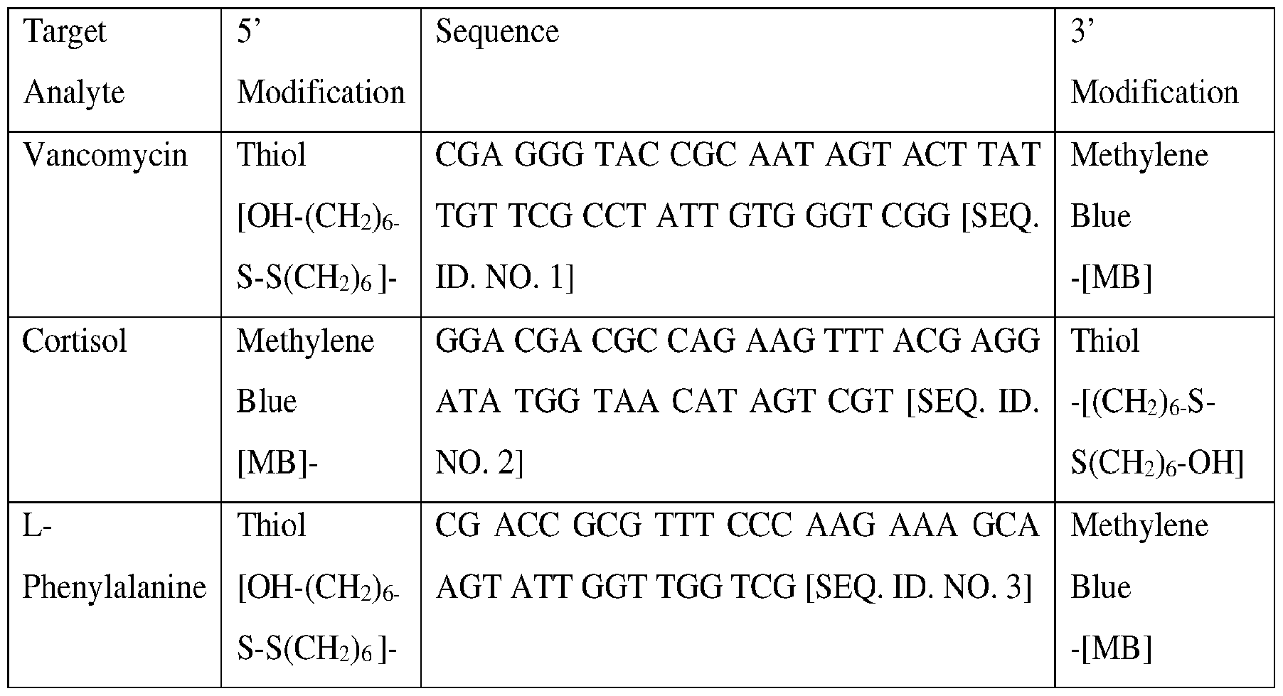
Sensor preparation
[0096] Gold electrodes with a titanium adhesion layer were deposited on PET or Kapton strips that provide a support for the electrodes. The gold was patterned via photolithography and chemical etching, and electrical insulators applied that were photo-defineable or screen-printable. The gold was further electroplated with additional gold and electrochemically roughened or cleaned prior to aptamer and protective layer incubation. Electrochemical cleaning was performed in a standard three-electrode electrochemical cell consisting of a gold working electrode, platinum counter electrode, and Ag/AgCl reference electrode by running 700 cyclic voltammetry scans in 0.5 M NaOH from -1 V to -1.6 V at a scan rate of 1 V/s and subsequently 150 scans in 0.5 M H2SO4 solution from 0V to 1.6 V at 1 V/s. Once the electrochemical cleaning was complete, electrodes were thoroughly rinsed with DI water, dried in a nitrogen stream (99.999% purity), and used for subsequent incubation. A lyophilized pellet of modified aptamer was diluted down to a 100 pM stock solution using TE buffer and kept at -20 °C until use. Preparation of aptamer working solution was performed by first mixing an aliquot of the 100 pM aptamer stock solution with equal volume of 0.5 M TCEP dissolved in Milli-Q water. The mixture was then set aside for Ihr to ensure complete reduction of any disulfide aptamer molecules. The obtained solution was then diluted to an intermediary concentration of ~4 uM with lx PBS/2 mM MgCh buffer and the
- 23 -
concentration confirmed via the absorbance measured at 260 nm using a Nanodrop UV/Vis Spectrophotometer. This solution was then subsequently diluted to 500 nM with lx PBS/2 mM MgCl 2 buffer for incubation of aptamer onto for one hour. The aptamer functionalized electrodes were then rinsed with DI water and incubated overnight at room temperature in 5 mM MCH or MCO prepared in lx PBS. The functionalized sensors were then rinsed with DI water prior to coating with trehalose for storage and ultimately then used for measurement. Electrochemical roughening and hydrogel protection was performed, prior to aptamer and MCH or MCO incubation, by immersing electrodes in 5 M NaOH solution and subjecting them to 20 ms long alternating potential steps of -5 V and +0.8 V (vs. Hg/Hg2SO4, sat. NaiSO^ respectively, for a total duration of 6000s in an electrochemical cell consisting of a Kapton®-carbon counter and saturated Hg/Hg2SO4 reference electrode. Once the roughening was completed, the electrodes were rinsed with copious amounts of DI water and aptamer and MCH or MCO then incubated as described above. Modification of the sensors with an antibiofouling zwitterionic polybetainebased hydrogel was performed by drop-casting 1 pL of the aqueous mixture consisting of monomer/cross-linker/photo-initiator (2.8g/1.8pl/36pl respectively dissolved in 1 ml of DI water) over the sensor and exposing it to UV light (X: 280-450 nm, Bluewave LEDPrime UVA, Dynamax, USA) for 45 min.
Electrochemical measurements
[0097] Electrochemical measurements were performed with a miniaturized potentiostat (details in FIG. 7) or performed by a benchtop CHI 620E potentiostat (Austin, Texas) connected to a 64-channel multiplexer in a standard three-electrode system with aptamer/alkylthiolate functionalized electrodes serving as working electrodes. The counter and reference electrodes were inserted into the skin using a platinum counter electrode, and a Ag/AgCl reference electrode, or alternately the counter and reference electrodes can be a large gel-electrode-pad electrode on the surface of the skin as taught in PCT/US21/51972 -‘APTAMER SENSORS WITH REFERENCE AND COUNTER VOLTAGE CONTROL’ . Cyclic voltammograms were recorded in a window from -0.1 V to -0.5 V at a scan rate of 100 mV/s. Square-wave voltammetry was performed in a potential window from -0.1 V to -0.5 V at 25 mV amplitude at the optimal frequency of measurement for each aptamer. FIG. 10A has a square waveform of frequency f and voltage amplitude Esw. This is superimposed on a staircase that ramps the mean voltage (the mean potential per pulse pair, E) by a voltage step size per cycle, Estep. In FIG. 10B in response to this varying voltage, the system produced an oscillating faradic current. This current was then
- 24 -
deconvoluted into “forward” and “backward” voltammograms by extracting the current at specific times after the capacitive background current had at least partially diminished (ifwd and ibwd). [0098] Kinetic differential measurmements, two frequency measurement, or continuous square wave voltammetry were utilized to improve calibration-free operation of the sensors. Example in-vivo data collected for a cortisol sensor inserted subcutaneously in a rat is shown in FIG. 11, where injections of cortisol were performed at 5 or 10 mg/kg.
Additional Targets With Stronger Binding Affinities and Slower Sensor Off Times [0099] The present invention applies generally to aptamer sensors (as described above) and other types of affinity biosensors, but is not limited to the specific examples taught herein. Available electrochemical sensors for analytes such as cortisol, vancomycin, phenylalanine, insulin, BNP, NT-proBNP, IL-6, C-peptide, C-Reactive protein, and sensors for other analyte targets may be incorporated in the present invention without limitation. Such aptamers can be obtained from the literature, by SELEX, or purchased from companies such as SOMAlogic, or BasePair Bio, or Dianox and adapted into the aptamer sensor similar to shown in FIG. 3 or other aptamer sensing configurations based on alternative switching mechanisms such as redox quenching, molecular pendulums, or other suitable methods. Generally, the principles of the present invention are most practically useful for aptamers with strong binding affinities (Kd values) in the nM, pM, and fM levels if it is desired to benefit from the present invention by reducing sensor off times. Generally, the principles of the present invention are practically useful for many aptamers regardless of binding affinity if it is desired to benefit from the present invention by shifting (increasing or decreasing) the apparent binding affinity.
[00100] For examples of aptamers with strong binding affinities, FIG. 12 illustrates the cumulative distribution function (CDF) and lower limit of quantification (LLOQ) for SomaLogic aptamers which are commercially available (from SomaLogic Operating Co., Inc., Boulder, CO). Many of these aptamers have binding affinity (Kd) values that are so low that the present invention is required to enable fast off times in biosensing applications. For example, the IL-6 aptamer from SomaLogic is publicly known and has a 200 pM binding affinity and can be thiol bonded to a gold working electrode with 6 or 8 carbon linkage and distally tagged with methylene blue, include a blocking layer such as mercaptooctanol, to make an aptamer sensor working electrode, using the sequence for the aptamer: 5’ GGCAGGZZEGGPAZZAACACGZZAAGZCGGZGG-idT-3’, where Z = benzyl, P = naphthyl, E = phenethyl chemical modifications of the natural aptamer bases. Using an aptamer such as the IL-6 aptamer or other strong binding affinity aptamers, the present invention may include a
- 25 -
first waveform and at least a second waveform, where during the first waveform or the second waveform the aptamer and the analyte will have a binding affinity during measurement that is at least less than 10 nM.
[00101] Although not described in detail herein, other steps which are readily interpreted from or incorporated along with the disclosed embodiments shall be included as part of the invention. The embodiments that have been described herein provide specific examples to portray inventive elements, but will not necessarily cover all possible embodiments commonly known to those skilled in the art.
- 26 -
12/5/24, 10:08 AM Sequence Listing
Sequence Listing
 file:///C:/Users/ggraff/AppData/Roaming/ST26_authoring/Project_9/generated.html
27
12/5/24, 10:08 AM Sequence Listing

28 file:///C:/Users/ggraff/AppData/Roaming/ST26_authoring/Project_9/generated.html 2/2
Claims
WHAT IS CLAIMED IS: 1. A method for continually sensing at least one analyte, comprising: bringing a sample including at least one analyte into contact with at least one sensor having an electrode and a plurality of aptamers that are capable of binding to the analyte, wherein at least some of the aptamers each carry at least one tag, and wherein each tag changes in at least one parameter when analyte binds to its associated aptamer; applying a first electronic waveform to the at least one sensor, wherein the first electronic waveform is associated with a first binding affinity between the analyte and the plurality of aptamers; and applying a second electronic waveform to the at least one sensor, wherein the second electronic waveform is associated with a second binding affinity between the analyte and the plurality of aptamers; whereinthe first electronic waveform and second electronic waveform are different waveforms, and wherein the first binding affinity and second binding affinity differ by at least 2X.
2. The method of claim 1, further comprising detecting the presence of analyte or measuring the concentration of analyte: (a) during and/or after applying the first electronic waveform, (b) during and/or after applying the second electronic waveform, or (c) during and/or after applying the first electronic waveform and during and/or after applying the second electronic waveform.
3. The method of claim 1 wherein each of the first and second waveforms are selected from the group consisting of: a. an analyte accumulation waveform; b. an analyte depletion waveform; c. an ion accumulation waveform; d. an ion depletion waveform; e. an aptamer repelling waveform; f. an aptamer attracting waveform; and g. an aptamer oscillating waveform.
4. The method of claim 1 wherein the first binding affinity is at least 2X stronger than the second binding affinity. - 27 -
5. The method of claim 1 wherein the first binding affinity is at least 3X stronger than the second binding affinity.
6. The method of claim 1 wherein the first binding affinity is at least 10X stronger than the second binding affinity.
7. The method of claim 1 wherein first waveform is associated with a first sensor off time and at least the second waveform is associated with a second sensor off, where the first and second sensor off times differ by at least 2X.
8. The method of claim 1 wherein first waveform is associated with a first sensor off time and at least the second waveform is associated with a second sensor off, where the first and second sensor off times differ by at least 5X.
9. The method of claim 1 wherein first waveform is associated with a first sensor off time and at least the second waveform is associated with a second sensor off, where the first and second sensor off times differ by at least 10X.
10. The method of claim 1 wherein the first waveform is applied less than at least one of <50, <20, <10, <5, <2, <1% of the time that the second waveform is applied.
11. The method of claim 1 wherein the second waveform promotes faster disassociation of the analyte and aptamers than the first waveform.
12. The method of claim 1 wherein the second waveform promotes greater binding of the analyte and the aptamers than the first waveform.
13. The method of claim 1 wherein during the first waveform or during the second waveform the aptamer and the analyte have a binding affinity that during measurement that is at least less than 10 nM.
14. The method of claim 1, wherein the first waveform comprises oscillating voltammetry with an oscillating frequency for a first period of time, resulting in a measurement of analyte concentration. - 28 -
15. The method of claim 14, wherein the oscillating frequency is less than 10 Hz.
16. The method of claim 14, wherein the oscillating frequency is less than 30 Hz.
17. The method of claim 14, wherein the first period of time is less than 1 minute.
18. The method of claim 14, wherein the first period of time is less than 10s.
19. The method of claim 14, wherein the first period of time is less than 1s.
20. The method of claim 1, wherein the first waveform is a cyclic voltammetry waveform.
21. The method of claim 1, wherein the first waveform is a chronoamperometry waveform.
22. The method of claim 1 wherein the first waveform is an analyte accumulation waveform.
23. The method of claim 1 wherein the first waveform is an analyte depletion waveform.
24. The method of claim 1 wherein the first waveform is an analyte depletion waveform.
25. The method of claim 1 wherein the first waveform is an aptamer oscillating waveform to disassociate aptamers and analytes.
26. The method of claim 25 wherein the second waveform is an analyte measurement waveform.
27. The method of claim 26 wherein first waveform is associated with a first sensor off time and the second waveform is associated with a second sensor off, where the first sensor off time is at least 2X faster than the second sensor off time. - 29 -
Applications Claiming Priority (4)
| Application Number | Priority Date | Filing Date | Title |
|---|---|---|---|
| US202363608090P | 2023-12-08 | 2023-12-08 | |
| US63/608,090 | 2023-12-08 | ||
| US202463712574P | 2024-10-28 | 2024-10-28 | |
| US63/712,574 | 2024-10-28 |
Publications (1)
| Publication Number | Publication Date |
|---|---|
| WO2025123003A1 true WO2025123003A1 (en) | 2025-06-12 |
Family
ID=95980577
Family Applications (1)
| Application Number | Title | Priority Date | Filing Date |
|---|---|---|---|
| PCT/US2024/059139 Pending WO2025123003A1 (en) | 2023-12-08 | 2024-12-09 | Advanced sampling methods for faster molecular sensor response to highly dilute analytes |
Country Status (1)
| Country | Link |
|---|---|
| WO (1) | WO2025123003A1 (en) |
Citations (3)
| Publication number | Priority date | Publication date | Assignee | Title |
|---|---|---|---|---|
| WO2021067779A1 (en) * | 2019-10-04 | 2021-04-08 | University Of Cincinnati | Shelf-stable, ready-to-use, electrochemical aptamer sensors |
| WO2022067051A1 (en) * | 2020-09-24 | 2022-03-31 | University Of Cincinnati | Aptamer sensors with reference and counter voltage control |
| WO2023205274A1 (en) * | 2022-04-19 | 2023-10-26 | University Of Cincinnati | Multimode sensor integration onto needle-based sensing systems |
-
2024
- 2024-12-09 WO PCT/US2024/059139 patent/WO2025123003A1/en active Pending
Patent Citations (4)
| Publication number | Priority date | Publication date | Assignee | Title |
|---|---|---|---|---|
| WO2021067779A1 (en) * | 2019-10-04 | 2021-04-08 | University Of Cincinnati | Shelf-stable, ready-to-use, electrochemical aptamer sensors |
| WO2022067051A1 (en) * | 2020-09-24 | 2022-03-31 | University Of Cincinnati | Aptamer sensors with reference and counter voltage control |
| US20230349894A1 (en) * | 2020-09-24 | 2023-11-02 | University Of Cincinnati | Reduced electronic sampling of aptamer sensors |
| WO2023205274A1 (en) * | 2022-04-19 | 2023-10-26 | University Of Cincinnati | Multimode sensor integration onto needle-based sensing systems |
Non-Patent Citations (2)
| Title |
|---|
| KUMAKLI HOPE, BALDWIN MARIE, ABEYKOON SANDUNI W., WHITE RYAN J.: "Microscale, Electrochemical, Aptamer-Based Sensors for Enhanced Small-Molecule Detection at Millisecond Time Scales", ACS SENSORS, AMERICAN CHEMICAL SOCIETY, US, vol. 8, no. 12, 22 December 2023 (2023-12-22), US, pages 4521 - 4530, XP093333132, ISSN: 2379-3694, DOI: 10.1021/acssensors.3c01055 * |
| SCHOUKROUN-BARNES LAUREN R, MACAZO FLORIKA C, GUTIERREZ BRENDA, LOTTERMOSER JUSTINE, LIU JUAN, WHITE RYAN J: "Reagentless, Structure-Switching Electrochemical Aptamer Based Sensors", ANNU REV ANAL CHEM (PALO ALTO CALIF). 2016 JUN 12; 9(1): 163Â181., 1 January 2016 (2016-01-01), XP093042794, DOI: 10.1146/annurev- * |
Similar Documents
| Publication | Publication Date | Title |
|---|---|---|
| Ye et al. | Nucleic acid-based wearable and implantable electrochemical sensors | |
| Koklu et al. | Organic bioelectronic devices for metabolite sensing | |
| Lin et al. | Wearable microneedle-based electrochemical aptamer biosensing for precision dosing of drugs with narrow therapeutic windows | |
| EP4072417B1 (en) | Devices and methods for aptamer-assisted microneedle-based monitoring of biomarkers | |
| JP5711141B2 (en) | Substrate concentration continuous measurement method | |
| Koudelka et al. | In vivo response of microfabricated glucose sensors to glycemia changes in normal rats. | |
| TW201038942A (en) | Wireless monitoring bio-diagnosis system | |
| Wang et al. | Label-free and sensitive thrombin sensing on a molecularly grafted aptamer on graphene | |
| JP2010528297A (en) | System and method for integrated electrochemical detection and electrical detection | |
| CN106572819A (en) | Electrochemical sensing system | |
| CN119907641A (en) | Wearable microfluidic bioaffinity sensors for automated molecular analysis | |
| Rousseau et al. | Perspective—Assessing electrochemical, aptamer-based sensors for dynamic monitoring of cellular signaling | |
| KR102488119B1 (en) | Bio sensor and manufacturing method thereof | |
| Paleček et al. | Ionic strength-dependent structural transition of proteins at electrode surfaces | |
| Kannan et al. | Ultrasensitive detection of l-cysteine using gold–5-amino-2-mercapto-1, 3, 4-thiadiazole core–shell nanoparticles film modified electrode | |
| Fan et al. | Iodide modified silver electrode and its application to the electroanalysis of hemoglobin | |
| US20250130196A1 (en) | Electrochemical Aptamer Sensors with Strong Sensor Response to Large Analytes | |
| Yang et al. | A needle-type sensor for monitoring glucose in whole blood. | |
| WO2025034769A1 (en) | Factory and in-vivo calibration of electrochemical aptamer sensors | |
| US20250116626A1 (en) | Electrochemical Aptamer Sensors with Signal Amplification Via Multiple Redox Tags | |
| JP2026507109A (en) | Biosensors for placement at non-predetermined skin depths - Patent Application 20070122997 | |
| Gerola et al. | Glucose biosensor based on multisegment nanowires exhibiting reversible magnetic control | |
| Tu | Wearable Sweat Sensors for Disease Monitoring and Management | |
| WO2026105844A1 (en) | Electrode and biosensor capable of measuring target analyte or uric acid with high sensitivity, and protein detection using electron from uric acid | |
| KR102175938B1 (en) | Glucose sensor fabricated on cylindrical single fiber |
Legal Events
| Date | Code | Title | Description |
|---|---|---|---|
| 121 | Ep: the epo has been informed by wipo that ep was designated in this application |
Ref document number: 24901703 Country of ref document: EP Kind code of ref document: A1 |