WO2025115656A1 - 半導体装置、電子機器、車両 - Google Patents
半導体装置、電子機器、車両 Download PDFInfo
- Publication number
- WO2025115656A1 WO2025115656A1 PCT/JP2024/040675 JP2024040675W WO2025115656A1 WO 2025115656 A1 WO2025115656 A1 WO 2025115656A1 JP 2024040675 W JP2024040675 W JP 2024040675W WO 2025115656 A1 WO2025115656 A1 WO 2025115656A1
- Authority
- WO
- WIPO (PCT)
- Prior art keywords
- output
- signal
- output switch
- circuit
- voltage
- Prior art date
- Legal status (The legal status is an assumption and is not a legal conclusion. Google has not performed a legal analysis and makes no representation as to the accuracy of the status listed.)
- Pending
Links
Images









Classifications
-
- H—ELECTRICITY
- H02—GENERATION; CONVERSION OR DISTRIBUTION OF ELECTRIC POWER
- H02H—EMERGENCY PROTECTIVE CIRCUIT ARRANGEMENTS
- H02H5/00—Emergency protective circuit arrangements for automatic disconnection directly responsive to an undesired change from normal non-electric working conditions with or without subsequent reconnection
- H02H5/04—Emergency protective circuit arrangements for automatic disconnection directly responsive to an undesired change from normal non-electric working conditions with or without subsequent reconnection responsive to abnormal temperature
-
- H—ELECTRICITY
- H02—GENERATION; CONVERSION OR DISTRIBUTION OF ELECTRIC POWER
- H02H—EMERGENCY PROTECTIVE CIRCUIT ARRANGEMENTS
- H02H7/00—Emergency protective circuit arrangements specially adapted for specific types of electric machines or apparatus or for sectionalised protection of cable or line systems, and effecting automatic switching in the event of an undesired change from normal working conditions
-
- H—ELECTRICITY
- H02—GENERATION; CONVERSION OR DISTRIBUTION OF ELECTRIC POWER
- H02J—ELECTRIC POWER NETWORKS; CIRCUIT ARRANGEMENTS OR SYSTEMS FOR SUPPLYING OR DISTRIBUTING ELECTRIC POWER; SYSTEMS FOR STORING ELECTRIC ENERGY
- H02J1/00—Circuit arrangements for DC mains or DC distribution networks
Definitions
- This disclosure relates to semiconductor devices, electronic devices, and vehicles.
- IPDs intelligent power devices
- SPSs smartt power switches
- a semiconductor device includes an output switch and an overcurrent protection circuit configured to detect an output current flowing through the output switch and apply overcurrent protection, the overcurrent protection circuit operates to limit the output current to a first overcurrent protection threshold or less until a first time has elapsed since an instruction to turn on the output switch has been issued or until a voltage across the output switch falls below a detection threshold, whichever occurs first, and when the voltage across the output switch falls below the detection threshold before the first time has elapsed since an instruction to turn on the output switch has been issued, the output current is limited to the first overcurrent protection threshold or less.
- the output switch When the output current exceeds a second overcurrent protection threshold that is greater than the overcurrent protection threshold, the output switch is forcibly turned off, and when the output current falls below the second overcurrent protection threshold, the output switch is released from the forced off state.
- the output current exceeds the second overcurrent protection threshold after the first time has elapsed since the output switch was instructed to turn on, or the number of times the output switch is forcibly turned off after the voltage across the output switch falls below the detection threshold reaches an upper limit, whichever comes first the output switch is forcibly turned off, and when the second time has elapsed, the output switch is released from the forced off state.
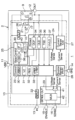
- FIG. 1 is a diagram showing an example of a configuration of an electronic device equipped with a semiconductor device.
- FIG. 2 is a diagram showing a first embodiment of a semiconductor device.
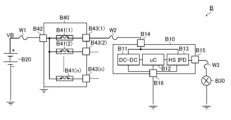
- FIG. 3 is a diagram showing an example of an electronic device equipped with a mechanical fuse.
- FIG. 4 is a diagram showing a second embodiment of the semiconductor device.
- FIG. 5 is a diagram showing a first example of the abnormality protection operation.
- FIG. 6 is a diagram showing a second example of the abnormality protection operation.
- FIG. 7 is a diagram showing a third example of the abnormality protection operation.
- FIG. 8 is a diagram showing a fourth example of the abnormality protection operation.
- FIG. 9 is a diagram showing a first example of a start-up operation in the second embodiment.
- FIG. 10 is a diagram showing a second example of the start-up operation in the second embodiment.
- FIG. 11 is a diagram showing a third example of the start-up operation in the second embodiment.
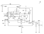
- FIG. 12 is a diagram showing a third embodiment of the semiconductor device.
- FIG. 13 is a diagram showing the turn-off behavior of the third embodiment.
- FIG. 14 is a diagram showing the startup behavior of the third embodiment.
- FIG. 15 is a partially enlarged view of a portion of FIG.
- FIG. 16 is a diagram showing a fourth embodiment of the semiconductor device.
- FIG. 17 is a diagram showing an example of generating a count completion signal.
- FIG. 18 is a diagram showing an example of the configuration of the control circuit.
- FIG. 19 is a diagram showing an example of generation of an upper limit count reached signal.
- FIG. 20 is a diagram showing an example of a mode transition.
- FIG. 21 is a diagram showing a first example of the start-up operation in the fourth embodiment.
- FIG. 22 is a diagram showing a second example of the start-up operation in the fourth embodiment.
- FIG. 23 is a diagram showing a third example of the start-up operation in the fourth embodiment.
- FIG. 24 is a diagram showing the external appearance of the vehicle.
- An electronic device A of this example includes a semiconductor device 1, a DC power source 2, and a load 3.
- the semiconductor device 1 is a high-side switch IC (a type of IPD) that connects/disconnects a DC power source 2 and a load 3, and is composed of an integrated power MISFET [metal insulator semiconductor field effect transistor] 9 and a controller 10.
- a high-side switch IC a type of IPD
- MISFET metal insulator semiconductor field effect transistor
- the semiconductor device 1 also has a number of external electrodes as means for establishing electrical connection with the outside of the device.
- the semiconductor device 1 has a drain electrode 11 (corresponding to the power supply electrode VBB), a source electrode 12 (corresponding to the output electrode OUT), an input electrode 13 (corresponding to the input electrode IN), and a reference voltage electrode 14 (corresponding to the ground electrode GND).
- the controller 10 includes multiple types of functional circuits that realize various functions.
- the multiple types of functional circuits include a circuit that generates a gate drive signal VG that drives and controls the power MISFET 9 based on an electrical signal from the outside.
- the drain electrode 11 transmits the power supply voltage VB to the drain of the power MISFET 9 and various circuits of the controller 10.
- the source electrode 12 is connected to the source of the power MISFET 9, and transmits the output voltage VOUT and the output current IOUT to the load 3.
- a signal line e.g., a wire harness laid between the source electrode 12 and the load 3 generally has an inductance component L (and a resistance component).
- the input electrode 13 transmits an input voltage (input signal) for driving the controller 10.
- the reference voltage electrode 14 transmits a reference voltage (e.g., a ground voltage) to the controller 10.
- a resistance component R generally accompanies the signal line between the reference voltage electrode 14 and the ground terminal.
- a light source such as a bulb lamp or an LED (light emitting diode) lamp
- the semiconductor device 1 includes a drain electrode 11, a source electrode 12, an input electrode 13, a reference voltage electrode 14, an enable electrode 15, a sense electrode 16, a gate control wiring 17, a power MISFET 9, and a controller 10.
- the drain electrode 11 provides a power supply voltage VB to the power MISFET 9 and the controller 10.
- the power supply voltage VB may be 10 V or more and 20 V or less.
- the input electrode 13 may be connected to an MCU [micro controller unit], a DC/DC converter, an LDO [low drop out] regulator, or the like.
- the input electrode 13 provides an input voltage to the controller 10.
- the input voltage may be 1 V or more and 10 V or less.
- the reference voltage electrode 14 is connected to a reference voltage wiring (ground terminal).
- the reference voltage electrode 14 provides a reference voltage to the power MISFET 9 and the controller 10.
- the enable electrode 15 may be connected to the MCU. An electrical signal for enabling or disabling some or all of the functions of the controller 10 is input to the enable electrode 15.
- the sense electrode 16 transmits an electrical signal for detecting an abnormality in the controller 10 to the outside of the device.
- the sense electrode 16 may be pulled up or down by a resistor.
- the gate of the power MISFET 9 is connected to the controller 10 (particularly the gate control circuit 25 described below) via the gate control wiring 17.
- the drain of the power MISFET 9 is connected to the drain electrode 11.
- the source of the power MISFET 9 is connected to the controller 10 (particularly the current detection circuit 27 described below) and the source electrode 12.
- the controller 10 includes a sensor MISFET 21, an input circuit 22, a current/voltage control circuit 23, a protection circuit 24, a gate control circuit 25, an active clamp circuit 26, a current detection circuit 27, a power supply reverse connection protection circuit 28, and an abnormality detection circuit 29.
- the gate of the sensor MISFET 21 is connected to the gate control circuit 25.
- the drain of the sensor MISFET 21 is connected to the drain electrode 11.
- the source of the sensor MISFET 21 is connected to the current detection circuit 27.
- the input circuit 22 is connected to the input electrode 13 and the current/voltage control circuit 23.
- the input circuit 22 may include a Schmitt trigger circuit.
- the input circuit 22 shapes the waveform of the electrical signal applied to the input electrode 13.
- the signal generated by the input circuit 22 is input to the current/voltage control circuit 23.
- the current/voltage control circuit 23 is connected to a protection circuit 24, a gate control circuit 25, a power supply reverse connection protection circuit 28, and an abnormality detection circuit 29.
- the current/voltage control circuit 23 may include a logic circuit.
- the current/voltage control circuit 23 generates various voltages in response to the electrical signal from the input circuit 22 and the electrical signal from the protection circuit 24.
- the current/voltage control circuit 23 includes a drive voltage generation circuit 30, a first constant voltage generation circuit 31, a second constant voltage generation circuit 32, and a reference voltage/reference current generation circuit 33.
- the drive voltage generation circuit 30 generates a drive voltage for driving the gate control circuit 25.
- the drive voltage may be set to a value obtained by subtracting a predetermined value from the power supply voltage VB.
- the drive voltage generation circuit 30 may generate a drive voltage between 5V and 15V, obtained by subtracting 5V from the power supply voltage VB.
- the drive voltage is input to the gate control circuit 25.
- the first constant voltage generating circuit 31 generates a first constant voltage for driving the protection circuit 24.
- the first constant voltage generating circuit 31 may include a Zener diode or a regulator circuit (here, a Zener diode).
- the first constant voltage may be 1 V or more and 5 V or less.
- the first constant voltage is input to the protection circuit 24 (more specifically, the load open detection circuit 35 described later, etc.).
- the second constant voltage generating circuit 32 generates a second constant voltage for driving the protection circuit 24.
- the second constant voltage generating circuit 32 may include a Zener diode or a regulator circuit (here, a regulator circuit).
- the second constant voltage may be 1 V or more and 5 V or less.
- the second constant voltage is input to the protection circuit 24 (more specifically, the overheat protection circuit 36 and the low voltage malfunction suppression circuit 37 described later).
- the reference voltage/reference current generating circuit 33 generates a reference voltage and a reference current for the various circuits.
- the reference voltage may be 1 V or more and 5 V or less.
- the reference current may be 1 mA or more and 1 A or less.
- the reference voltage and the reference current are input to the various circuits. If the various circuits include a comparator, the reference voltage and the reference current may be input to the comparator.
- the protection circuit 24 is connected to the current/voltage control circuit 23, the gate control circuit 25, the abnormality detection circuit 29, the source of the power MISFET 9, and the source of the sensor MISFET 21.
- the protection circuit 24 includes an overcurrent protection circuit 34, an open load detection circuit 35, an overheat protection circuit 36, and an undervoltage malfunction suppression circuit 37.
- the overcurrent protection circuit 34 protects the power MISFET 9 from an overcurrent.
- the overcurrent protection circuit 34 is connected to the gate control circuit 25 and the source of the sensor MISFET 21.
- the overcurrent protection circuit 34 may include a current monitor circuit.
- the signal generated by the overcurrent protection circuit 34 is input to the gate control circuit 25 (more specifically, the drive signal output circuit 40 described later).
- the load open detection circuit 35 detects the short state and open state of the power MISFET 9.
- the load open detection circuit 35 is connected to the current/voltage control circuit 23 and the source of the power MISFET 9.
- the signal generated by the load open detection circuit 35 is input to the current/voltage control circuit 23.
- the overheat protection circuit 36 monitors the temperature of the power MISFET 9 and protects the power MISFET 9 from an excessive temperature rise.
- the overheat protection circuit 36 is connected to the current/voltage control circuit 23.
- the overheat protection circuit 36 may include a temperature sensing device such as a temperature sensing diode or a thermistor.
- the signal generated by the overheat protection circuit 36 is input to the current/voltage control circuit 23.
- the low-voltage malfunction suppression circuit 37 suppresses malfunction of the power MISFET 9 when the power supply voltage VB is less than a predetermined value.
- the low-voltage malfunction suppression circuit 37 is connected to the current/voltage control circuit 23.
- the signal generated by the low-voltage malfunction suppression circuit 37 is input to the current/voltage control circuit 23.
- the gate control circuit 25 controls the on and off states of the power MISFET 9 and the on and off states of the sensor MISFET 21.
- the gate control circuit 25 is connected to the current/voltage control circuit 23, the protection circuit 24, the gate of the power MISFET 9, and the gate of the sensor MISFET 21.
- the gate control circuit 25 outputs a gate drive signal VG to the gate control wiring 17 in response to an electrical signal from the current/voltage control circuit 23 and an electrical signal from the protection circuit 24.
- the gate drive signal VG is input to the gate of the power MISFET 9 and the gate of the sensor MISFET 21 via the gate control wiring 17.
- the gate control circuit 25 turns the power MISFET 9 on and off by controlling the gate drive signal VG in response to an electrical signal (input signal) applied to the input electrode 13.
- the gate control circuit 25 includes an oscillation circuit 38, a charge pump circuit 39, and a drive signal output circuit 40.
- the oscillation circuit 38 oscillates in response to an electrical signal from the current/voltage control circuit 23, and generates a predetermined electrical signal.
- the electrical signal generated by the oscillation circuit 38 is input to the charge pump circuit 39.
- the charge pump circuit 39 generates a boost voltage VCP based on the electrical signal from the oscillation circuit 38.
- the boost voltage VCP generated by the charge pump circuit 39 is input to the drive signal output circuit 40.
- the drive signal output circuit 40 operates by receiving the boosted voltage VCP output from the charge pump circuit 39, and generates a gate drive signal VG in response to an electrical signal from the protection circuit 24 (more specifically, the overcurrent protection circuit 34).
- the gate drive signal VG is input to the gate of the power MISFET 9 and the gate of the sensor MISFET 21 via the gate control wiring 17.
- the sensor MISFET 21 and the power MISFET 9 are simultaneously controlled by the gate control circuit 25.
- the active clamp circuit 26 protects the power MISFET 9 from back electromotive force.
- the active clamp circuit 26 is connected to the drain electrode 11, the gate of the power MISFET 9, and the gate of the sensor MISFET 21.
- the active clamp circuit 26 may include multiple diodes.
- the active clamp circuit 26 may include a plurality of diodes connected in a forward bias to each other.
- the active clamp circuit 26 may include a plurality of diodes connected in a reverse bias to each other.
- the active clamp circuit 26 may include a plurality of diodes connected in a forward bias to each other, and a plurality of diodes connected in a reverse bias to each other.
- the multiple diodes may include pn junction diodes, or Zener diodes, or pn junction diodes and Zener diodes.
- the active clamp circuit 26 may include multiple Zener diodes connected to each other in a biased manner.
- the active clamp circuit 26 may include Zener diodes and pn junction diodes connected to each other in a reverse biased manner.
- the current detection circuit 27 detects the current flowing through the power MISFET 9 and the sensor MISFET 21.
- the current detection circuit 27 is connected to the protection circuit 24, the abnormality detection circuit 29, the source of the power MISFET 9, and the source of the sensor MISFET 21.
- the current detection signal is input to the abnormality detection circuit 29.
- the power supply reverse connection protection circuit 28 protects the current/voltage control circuit 23 and the power MISFET 9 from reverse voltage when the DC power supply 2 is reverse connected.
- the power supply reverse connection protection circuit 28 is connected to the reference voltage electrode 14 and the current/voltage control circuit 23.
- the abnormality detection circuit 29 monitors the voltage of the protection circuit 24.
- the abnormality detection circuit 29 is connected to the current/voltage control circuit 23, the protection circuit 24, and the current detection circuit 27. If an abnormality (such as a voltage fluctuation) occurs in any of the overcurrent protection circuit 34, the open load detection circuit 35, the overheat protection circuit 36, and the low voltage malfunction suppression circuit 37, the abnormality detection circuit 29 generates an abnormality detection signal according to the voltage of the protection circuit 24 and outputs it to the outside.
- the abnormality detection circuit 29 includes a first multiplexer circuit 41 and a second multiplexer circuit 42.
- the first multiplexer circuit 41 includes two input sections, one output section, and one selection control input section.
- the protection circuit 24 and the current detection circuit 27 are respectively connected to the input section of the first multiplexer circuit 41.
- the second multiplexer circuit 42 is connected to the output section of the first multiplexer circuit 41.
- the current/voltage control circuit 23 is connected to the selection control input section of the first multiplexer circuit 41.
- the first multiplexer circuit 41 generates an abnormality detection signal in response to the electrical signal from the current/voltage control circuit 23, the voltage detection signal from the protection circuit 24, and the current detection signal from the current detection circuit 27.
- the abnormality detection signal generated by the first multiplexer circuit 41 is input to the second multiplexer circuit 42.
- the second multiplexer circuit 42 includes two inputs and one output.
- the inputs of the second multiplexer circuit 42 are connected to the output of the second multiplexer circuit 42 and the enable electrode 15, respectively.
- the output of the second multiplexer circuit 42 is connected to the sense electrode 16.
- an MCU When an MCU is connected to the enable electrode 15 and a pull-up or pull-down resistor is connected to the sense electrode 16, an on signal is input from the MCU to the enable electrode 15, and an abnormality detection signal is extracted from the sense electrode 16.
- the abnormality detection signal is converted into an electrical signal by the resistor connected to the sense electrode 16. An abnormal state of the semiconductor device 1 is detected based on this electrical signal.
- An electronic device B of this configuration example includes a control unit B10, a battery B20, a load B30, and a fuse box B40.
- the control unit B10 drives the load B30 by receiving a power supply voltage VB from the battery B20 via the fuse box B40.
- the control unit B10 includes a DC/DC converter B11, a microcomputer B12, an upper switch B13, a power supply electrode B14, an output electrode B15, and a reference voltage electrode B16.
- the control unit B10 may be, for example, an ECU [electronic control unit].
- the DC/DC converter B11 generates the desired internal power supply voltage from the power supply voltage VB and outputs it to each part of the control unit B10 (such as the microcomputer B12).
- the microcontroller B12 receives an internal power supply voltage from the DC/DC converter B11 and controls the on/off of the upper switch B13.
- the upper switch B13 is connected between the power supply electrode B14 and the output electrode B15, and is controlled to be turned on/off according to instructions from the microcomputer B12.
- the power supply electrode B14 receives the power supply voltage VB from the battery B20 via the fuse box B40.
- the output electrode B15 is connected to the load B30, for example, via the wire W3.
- the reference voltage electrode B16 is connected to the ground terminal, for example.
- the fuse box B40 includes n fuses B41(1) to B41(n), an input electrode B42, and output electrodes B43(1) to B43(n).
- Fuse B41(i) is a so-called mechanical fuse, and when a current exceeding the rated value flows through it, it melts down due to Joule heat to protect the circuit.
- the output electrode B43(1) is connected to the power supply electrode B14 of the control unit B10 via, for example, a wire W2.
- control unit B10 In order to solve the above problem, it is possible to use an electronic fuse (so-called e-fuse) using an IPD instead of a mechanical fuse.
- the control unit B10 often has its own input capacitor in the subsystem such as the DC/DC converter B11. Therefore, from the perspective of the electronic fuse, the control unit B10 functions as a capacitive load with a large capacitance value (generally in the mF range).
- Semiconductor Device (Second Embodiment) 4 is a diagram showing a second embodiment of the semiconductor device 1 (i.e., a configuration example of the semiconductor device 1 replacing a mechanical fuse).
- the fuse box B40 is replaced with the semiconductor device 1, based on the electronic device B shown in FIG.
- the semiconductor device 1 has a configuration similar to that of the first embodiment (FIG. 2) described above, and further includes a CMODE enable electrode 51, an input circuit 52, and a mode control circuit 53. Therefore, the components already described are given the same reference numerals as those in FIG. 2 to avoid redundant explanations, and the following description will focus on new components and components related to them.
- the power MISFET 9 is an output switch that connects/disconnects the drain electrode 11 and the source electrode 12 in response to the gate drive signal VG.
- the overcurrent protection circuit 34 detects the output current IOUT flowing through the power MISFET 9 and controls the gate drive signal VG to apply overcurrent protection.
- the overheat protection circuit 36 detects the monitored temperature and controls the gate drive signal VG to apply overheat protection.
- the temperature to be monitored may be a first temperature Temp1 detected in the power element formation region including the power MISFET 9.
- the first temperature Temp1 may be, for example, a pn junction temperature Tj1 in the power element formation region.
- the second temperature Temp2 may be, for example, the pn junction temperature Tj2 of the analog circuit formation region or the logic circuit formation region, or the case temperature Tc of the semiconductor device 1 or the ambient temperature Ta.
- the CMODE enable electrode 51 is an external electrode for switching the mode control circuit 53 between enabled and disabled.
- the input circuit 52 shapes the waveform of the electrical signal applied to the CMODE enable electrode 51 and outputs it to the mode control circuit 53.
- the mode control circuit 53 generates a mode control signal S1 for switching between setting the overcurrent protection circuit 34 and the overheat protection circuit 36 to normal mode or capacitive load drive mode.
- the mode control signal S1 is output to each of the overcurrent protection circuit 34 and the overheat protection circuit 36.
- the mode control circuit 53 is enabled, for example, when the electrical signal applied to the CMODE enable electrode 51 is at a high level, and is in a state in which the logical level of the mode control signal S1 can be switched.
- the overcurrent protection circuit 34 and the overheat protection circuit 36 are set to the normal mode when the mode control signal S1 is at a high level, and are set to the capacitive load drive mode when the mode control signal S1 is at a low level.
- the overcurrent protection circuit 34 performs a current limiting operation to limit the output current IOUT to less than or equal to the overcurrent protection threshold Iocp.
- the overheat protection circuit 36 also repeatedly forcibly turns off and restarts the power MISFET 9 each time the monitored temperature (for example, the aforementioned temperature difference ⁇ Temp) rises to the overheat protection threshold Ttsd.
- the mode control circuit 53 is disabled, for example, when the electrical signal applied to the CMODE enable electrode 51 is at a low level. In this case, the mode control signal S1 is fixed at a high level. Therefore, the overcurrent protection circuit 34 and the overheat protection circuit 36 are set to the normal mode.
- the fuse box B40 mentioned above is replaced with the semiconductor device 1. That is, if the output current IOUT becomes excessive (for example, several tens to 100 A), the power MISFET 9 is forcibly turned off, thereby limiting or cutting off the output current IOUT quickly and accurately. Therefore, both the semiconductor device 1 and the control unit B10 can be safely protected. Also, unlike a configuration using a mechanical fuse, there is no need to replace a blown fuse B41(i) even if a failure occurs.
- the semiconductor device 1 has a capacitive load drive mode as one of its operation modes. Therefore, it can appropriately drive a capacitive load (control unit B10 in this figure) without increasing the size of the power MISFET 9 or requiring additional external components.
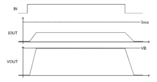
- this diagram shows the behavior when a resistive load (or an inductive load) is driven by the semiconductor device 1 of the second embodiment (FIG. 4).
- the output voltage VOUT rises to the power supply voltage VB.
- the output current IOUT reaches the target value (nominal value) without exceeding the overcurrent protection threshold Iocp.
- the behavior of the semiconductor device 1 differs depending on whether the overcurrent protection circuit 34 and the overheat protection circuit 36 are set to normal mode or capacitive load drive mode.
- this diagram shows the behavior when a capacitive load (e.g., control unit B10) is driven by the semiconductor device 1 of the second embodiment (FIG. 4).
- This diagram also shows that the electrical signal applied to the CMODE enable electrode 51 is at a low level, and the mode control signal S1 is fixed at a high level.
- this diagram shows the behavior when the overcurrent protection circuit 34 and the overheat protection circuit 36 are set to normal mode.
- this figure shows the behavior of a capacitive load (e.g., control unit B10) when driven by the semiconductor device 1 of the second embodiment (FIG. 4).
- a capacitive load e.g., control unit B10
- the overcurrent protection circuit 34 and the overheat protection circuit 36 are set to normal mode.
- the overcurrent protection operation in normal mode is different from that described above.
- this figure like the above-mentioned Figures 6 and 7, shows the behavior when a capacitive load (e.g., control unit B10) is driven by the semiconductor device 1 of the second embodiment ( Figure 4).
- a capacitive load e.g., control unit B10
- the overcurrent protection circuit 34 and the overheat protection circuit 36 are set to the capacitive load drive mode rather than the normal mode.
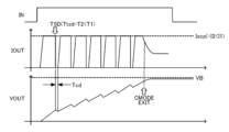
- both the overcurrent protection threshold Iocp and the overheat protection threshold Ttsd are lowered below those in the normal mode, and the power MISFET 9 is repeatedly forced off and restarted.
- the capacitive load drive mode makes it possible to properly drive capacitive loads that are difficult to drive in normal mode.
- the overcurrent protection threshold Iocp and the overheat protection threshold Ttsd are lowered compared to the normal mode. Therefore, while the capacitive load is being charged, the semiconductor device 1 and the capacitive load connected thereto (e.g., the control unit B10) are maintained in a safe operation area (SOA [safety operation area]).
- SOA safe operation area
- At least one of the second overcurrent protection threshold Iocp2 and the second overheat protection threshold Ttsd2 may be raised stepwise to the first overcurrent protection threshold Iocp1 and the first overheat protection threshold Ttsd1 in response to an increase in the output voltage VOUT or over time.
- the mode control circuit 53 may switch the overcurrent protection circuit 34 and the overheat protection circuit 36 from the capacitive load drive mode to the normal mode when a specific recovery condition (described in detail later) is satisfied (see “CMODE EXIT" in the figure).
- Iocp overcurrent protection threshold
- Iocp overcurrent protection threshold
- the semiconductor device 1 of this configuration example can switch between normal mode and capacitive load drive mode as needed. Therefore, for example, the on-resistance of the power MISFET 9 is relatively high, and it is compatible with process technologies that require stricter overcurrent protection operations.
- the overcurrent protection threshold Iocp is lowered (Iocp1 ⁇ Iocp2). This reduces the peak of the inrush current flowing through the capacitive load during charging.
- the above ratio is not limited to the above in any way.
- the overheat protection threshold Ttsd is lowered (Ttsd1 ⁇ Ttsd2). This has two effects. The first is that the semiconductor device 1 is maintained in the safe operating area while the capacitive load is not fully charged, i.e., while the capacitive load is functioning as a virtual short circuit. The second is that the semiconductor device 1 is quickly cooled to the overheat release temperature (safety temperature), so that the timing for restarting the power MISFET 9 is advanced and the capacitive load can continue to be charged. In other words, a charge pump effect is obtained, so that the output voltage VOUT can be reliably raised.
- the overheat release temperature safety temperature
- the capacitive load drive mode is automatically restored to the normal mode.
- the above threshold voltage Vth corresponds to the termination threshold of the capacitive load drive mode.
- the overcurrent protection operation after the return to the normal mode can be any of the current limiting operation, the hiccup operation, and the off-latch operation.
- the normal mode may be automatically restored when a predetermined time (e.g., 50 ms) has elapsed since the capacitive load drive mode was set. This allows the semiconductor device 1 to be maintained within a safe operating area even if an output short circuit or other fault occurs.
- a predetermined time e.g. 50 ms
- the semiconductor device 1 includes a CMODE enable electrode 51 for switching between enabling and disabling the mode control circuit 53 (and thus the capacitive load drive mode). This allows the user to freely decide whether or not to use the capacitive load drive mode. Furthermore, the mode control circuit 53 can be easily switched between enabling and disabling without applying any special gimmick (such as high-frequency PWM [pulse width modulation] drive or multi-level input) to the input electrode IN.
- any special gimmick such as high-frequency PWM [pulse width modulation] drive or multi-level input
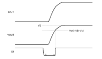
- ⁇ Startup operation> 9 is a diagram showing a first example of the startup operation of the semiconductor device 1 according to the second embodiment (FIG. 4). In this diagram, from the top, an output current IOUT, an output voltage VOUT, and a mode control signal S1 are depicted.
- the mode control circuit 53 drops the mode control signal S1 to a low level when the power MISFET 9 transitions to an on state. Therefore, the overcurrent protection circuit 34 and the overheat protection circuit 36 are set to the capacitive load drive mode described above. Note that the capacitive load drive mode does not have any effect on the drive operation (e.g., slew rate) of the resistive load.
- the mode control circuit 53 raises the mode control signal S1 to a high level. This switches the overcurrent protection circuit 34 and the overheat protection circuit 36 from the capacitive load drive mode to the normal mode.
- the above-mentioned recovery condition is that the output voltage VOUT is detected to be higher than a predetermined threshold voltage Vth.
- Vth VB - Vx
- Vx bias voltage
- the above recovery condition may also be that a predetermined time (e.g., 50 ms) has elapsed since the mode control signal S1 was lowered to a low level.
- a predetermined time e.g., 50 ms
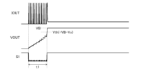
- FIG. 10 is a diagram showing a second example of the startup operation of the semiconductor device 1 of the second embodiment (FIG. 4).
- the output current IOUT, the output voltage VOUT, and the mode control signal S1 are depicted from the top.
- the on-resistance of the power MISFET 9 is 4 m ⁇ .
- the mode control signal S1 is pulled down to a low level, and the overcurrent protection circuit 34 and the overheat protection circuit 36 are set to the capacitive load drive mode.
- This causes the output voltage VOUT to rise to the threshold voltage Vth within the required start-up time t1 (e.g., less than 2 ms).
- the conditions for returning from the capacitive load drive mode to the normal mode are the same as above.
- FIG. 11 is a diagram showing a third example of the startup operation of the semiconductor device 1 of the second embodiment (FIG. 4).
- the output current IOUT, the output voltage VOUT, and the mode control signal S1 are depicted from the top.
- the on-resistance of the power MISFET 9 is 4 m ⁇ .
- the mode control signal S1 is pulled down to a low level, and the overcurrent protection circuit 34 and the overheat protection circuit 36 are set to the capacitive load drive mode.
- This causes the output voltage VOUT to rise to the threshold voltage Vth within the required start-up time t2 (e.g., less than 7.5 ms).
- the conditions for returning from the capacitive load drive mode to the normal mode are the same as above.
- ⁇ Semiconductor Device (Third Embodiment)> 12 is a diagram showing a third embodiment (corresponding to a comparative example to be compared with the fourth embodiment described later) of the semiconductor device 1.
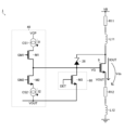
- the semiconductor device 1 of this embodiment is based on the second embodiment (FIG. 4) described above and further includes a high speed turn-off circuit 60.
- transistor M1 e.g., a P-channel MISFET
- transistor M2 e.g., an N-channel MISFET
- current sources CS1 and CS2 are clearly shown as components of the drive signal output circuit 40.
- a resistance component R11 and an inductance component L11 of the wire harness are depicted between the application terminal of the power supply voltage VB and the drain of the power MISFET 9.
- a resistance component R12 and an inductance component L12 of the wire harness are depicted between the source of the power MISFET 9 and a reference potential terminal (e.g., a ground terminal).
- the source of transistor M1 is connected to the application terminal of boost voltage VCP via current source CS1.
- the source of transistor M2 is connected to the application terminal of output voltage VOUT via current source CS2.
- the gate of transistor M1 is connected to the application terminal of gate voltage GM1.
- the gate of transistor M2 is connected to the application terminal of gate voltage GM2. Note that gate voltages GM1 and GM2 can each be understood as being supplied from current/voltage control circuit 23.
- Transistors M1 and M2 connected in this way form a half-bridge output stage of the drive signal output circuit 40.
- transistor M1 provides conduction/cutoff between current source CS1 and the gate of power MISFET 9 in response to gate voltage GM1.
- Transistor M2 provides conduction/cutoff between the gate of power MISFET 9 and current source CS2 in response to gate voltage GM2.
- the gate voltages GM1 and GM2 are both at a low level.
- the transistor M1 is turned on and the transistor M2 is turned off.
- the gate capacitance (not shown) of the power MISFET 9 is charged by the first current I1 that flows from the application terminal of the boost voltage VCP through the current source CS1 and the transistor M1 to the gate of the power MISFET 9. Therefore, the gate drive signal VG becomes a high level ( ⁇ VCP). As a result, the power MISFET 9 is turned on.
- the gate voltages GM1 and GM2 are both at a high level. Therefore, the transistor M1 is turned off, and the transistor M2 is turned on. At this time, the gate capacitance (not shown) of the power MISFET 9 is discharged by the second current I2 that flows from the gate of the power MISFET 9 through the transistor M2 and the current source CS2 to the application terminal of the output voltage VOUT. Therefore, the gate drive signal VG becomes a low level ( ⁇ VOUT). As a result, the power MISFET 9 is turned off.
- transistors M1 and M2 are complementarily turned on/off in response to the electrical signal (input signal) applied to the input electrode 13, and thus the gate voltages GM1 and GM2.
- the high-speed turn-off circuit 60 quickly turns off the power MISFET 9 with a second gate discharge capability higher than the first gate discharge capability of the drive signal output circuit 40 in response to an abnormality detection signal DET (e.g., an overcurrent protection signal or an overheat protection signal).
- DET an abnormality detection signal
- the high speed turn-off circuit 60 includes a transistor M3 (e.g., an N-channel MISFET).
- the drain of the transistor M3 is connected to the gate of the power MISFET 9.
- the gate of the transistor M3 is connected to the application terminal of the abnormality detection signal DET.
- Transistor M3 connected in this manner connects/disconnects the gate and source of power MISFET 9 in response to the abnormality detection signal DET.
- the gate drive signal VG is pulled down to a low level ( ⁇ VOUT) without delay via the transistor M3 without relying on the drive signal output circuit 40. Therefore, the power MISFET 9 is turned off at high speed in a shorter time than in a normal turn-off using the drive signal output circuit 40.
- the transistor M3 is in an off state. Therefore, there is no problem with the charge/discharge control of the gate drive signal VG by the drive signal output circuit 40.
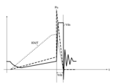
- FIG. 13 is a diagram showing the turn-off behavior of the semiconductor device 1 of the third embodiment (FIG. 12).
- the solid line is the drain-source voltage Vds of the power MISFET 9.
- the small dashed line is the output current IOUT flowing through the power MISFET 9.
- an abnormality protection operation e.g., an overcurrent protection operation or an overheat protection operation.
- the active clamp circuit 26 operates to return the power MISFET 9 to the on state (strictly speaking, the power MISFET 9 is not fully turned off).
- the power MISFET 9 is maintained in the on state until the inductive energy stored in the inductance component of the load short-circuit path is dissipated (which may be understood as regeneration, absorption, or consumption).
- the semiconductor device 1 must also control the turn-off of the power MISFET 9 so that the instantaneous maximum junction temperature does not exceed the absolute maximum rating.
- the maximum peak value of the power consumption Pc becomes relatively large due to the high-speed turn-off of the power MISFET 9.
- the total power consumption (total energy) that needs to be safely dissipated by the active clamp operation is reduced.
- the maximum junction temperature of the power MISFET 9 is reduced. In this way, the introduction of the high-speed turn-off circuit 60 makes it possible to improve the harness ground fault tolerance.
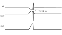
- Fig. 14 is a diagram showing the startup behavior of the semiconductor device 1 in the third embodiment (Fig. 12).
- Fig. 15 is a partially enlarged diagram of a part (a dashed-dotted line frame ⁇ ) of Fig. 14. In both diagrams, the power supply voltage VB, the output voltage VOUT, and the output current IOUT are depicted from the top.
- the semiconductor device 1 is started in the capacitive load drive mode.
- the drain-source voltage Vds of the power MISFET 9 is likely to decrease. This causes the timing of switching from the capacitive load drive mode to the normal mode to be accelerated, which may cause a start-up failure of the capacitive load.
- a fourth embodiment is proposed that can eliminate the start-up failure of the capacitive load.
- Semiconductor Device (Fourth Embodiment) 16 is a diagram showing a fourth embodiment of the semiconductor device 1.
- an overcurrent protection circuit 34 detects an output current IOUT flowing through a power MISFET 9 (corresponding to an output switch) and applies overcurrent protection.
- the overcurrent protection circuit 34 includes a detection circuit 341, a control circuit 342, and an output circuit 343 as components for performing the overcurrent protection operation after the capacitive load drive mode ends, more specifically, for performing the forced off control of the power MISFET 9, including the hiccup operation described above.
- the detection circuit 341 outputs an internal signal S11 according to the result of comparing the output current IOUT with the overcurrent protection threshold IocpH, for example, after the mode control signal S1 output from the mode control circuit 53 falls from high to low.
- the detection circuit 341 may also receive an input of a sense voltage Vs ( ⁇ IOUT) according to the output current IOUT.
- the mode control signal S1 is at a high level in the capacitive load driving mode described above, and is at a low level after the capacitive load driving mode ends.
- the logical level of the mode control signal S1 may be the opposite to that shown in the examples of the second embodiment ( Figures 9 to 11).
- the internal signal S11 is at a high level, for example, when the output current IOUT is greater than the overcurrent protection threshold IocpH. On the other hand, the internal signal S11 is at a low level when the output current IOUT is less than the overcurrent protection threshold IocpH. However, when the mode control signal S1 is at a high level, the internal signal S11 is fixed (masked) at a low level.
- the overcurrent protection threshold IocpH may be set to a value (e.g., 90 A) greater than the overcurrent protection threshold IocpL (e.g., 60 A) set in the capacitive load drive mode.
- the overcurrent protection threshold IocpH may have hysteresis.
- the control circuit 342 receives, for example, the mode control signal S1 and count completion signal S2 output from the mode control circuit 53, and the internal signal S11 output from the detection circuit 341, and outputs the internal signal S12.
- the internal configuration and operation of the control circuit 342 will be described later.
- FIG. 17 shows an example of generating the count completion signal S2. This figure shows the terminal voltages (IN/CMODE) of the input electrode 13 and the CMODE enable electrode 51, the mode control signal S1, and the count completion signal S2.
- the mode control circuit 53 starts counting time T1 (e.g., 50 ms).
- time T1 e.g. 50 ms.
- a CR timer or the like may be used as the means for measuring time T1.
- the mode control signal S1 is pulled down to a low level. That is, the capacitive load drive mode is terminated not only when the drain-source voltage Vds of the power MISFET 9 falls below the detection threshold Vx, but also when time T1 has elapsed. In this case, the semiconductor device 1 transitions from the capacitive load drive mode to the normal mode without passing through the intermediate mode (details of which will be described later).
- a pulse is generated in the count completion signal S2 when a time T1 has elapsed since the power MISFET 9 was instructed to be turned on.
- the output circuit 343 receives the internal signals S11 and S12 and outputs a forced-off signal S34 for the power MISFET 9.
- the forced off signal S34 is at a low level when the internal signal S11 is at a high level, and is at a high level when the internal signal S11 is at a low level.
- the forced off signal S34 is also maintained at a low level for a time T2 (e.g., 50 ms) after a pulse is generated in the internal signal S12 (details will be described later).
- the drive signal output circuit 40 forcibly turns off the power MISFET 9 when the forced-off signal S34 is at a low level, for example. On the other hand, the drive signal output circuit 40 releases the forced-off state of the power MISFET 9 when the forced-off signal S34 is at a high level, for example.
- the overcurrent protection circuit 34 also includes components for performing overcurrent protection operation in the capacitive load drive mode, more specifically, a current limiting operation that pulls down the gate drive signal VG of the power MISFET 9 to limit the output current IOUT to less than or equal to the overcurrent protection threshold Iocp.
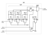
- FIG. 18 is a diagram showing an example of the configuration of the control circuit 342.
- the control circuit 342 in this example configuration includes a logical product operator AND, D flip-flops FF1 to FF4, inverters INV1 to INV3, a multiplexer MUX, and a logical negative sum operator NOR.
- D flip-flop FF1 latches the inverted output signal XQ1 input to the data terminal (D) when the internal signal S11 input to the clock terminal (>) rises to a high level, and outputs it as the output signal Q1 from the output terminal (Q). D flip-flop FF1 also resets the output signal Q1 to a low level when the reset signal RST input to the reset terminal (O) falls to a low level, for example.
- the D flip-flop FF2 latches the inverted output signal XQ2 input to the data terminal (D) when the inverted output signal XQ1 input to the clock terminal (>) rises to a high level, and outputs it as an output signal Q2 from the output terminal (Q).
- the D flip-flop FF2 also resets the output signal Q2 to a low level when the reset signal RST input to the reset terminal (O) falls to a low level, for example.
- the D flip-flop FF3 latches the inverted output signal XQ3 input to the data terminal (D) when the inverted output signal XQ2 input to the clock terminal (>) rises to a high level, and outputs it as an output signal Q3 from the output terminal (Q).
- the D flip-flop FF3 also resets the output signal Q2 to a low level when the reset signal RST input to the reset terminal (O) falls to a low level, for example.
- the D flip-flop FF4 latches the high level signal VH input to the data terminal (D) and outputs it as an output signal Q4 from the output terminal (Q).
- the D flip-flop FF4 resets the output signal Q4 to a low level when, for example, the intermediate mode completion signal S22 input to the reset terminal (O) falls to a low level.
- Inverter INV1 generates an inverted output signal XQ1 by inverting the logic level of output signal Q1.
- Inverter INV2 generates an inverted output signal XQ2 by inverting the logic level of output signal Q2.
- Inverter INV3 generates an inverted output signal XQ3 by inverting the logic level of output signal Q3.
- the logical product operator AND generates the upper limit count reached signal S21 by performing a logical product operation on each of the output signals Q1 to Q3.
- the upper limit count reached signal S21 is at high level when all of the output signals Q1 to Q3 are at high level.
- the upper limit count reached signal S21 is at low level when at least one of the output signals Q1 to Q3 is at low level.
- the NOR logic unit NOR generates the intermediate mode expiration signal S22 by performing a NOR operation on the count expiration signal S2 and the upper limit count reached signal S21.
- the intermediate mode expiration signal S22 becomes low level when at least one of the count expiration signal S2 and the upper limit count reached signal S21 is at high level.
- the intermediate mode expiration signal S22 becomes high level when both the count expiration signal S2 and the upper limit count reached signal S21 are at low level.
- the multiplexer MUX selects and outputs either the output signal Q1 or the upper limit count reached signal S21 as the internal signal S12 in response to the output signal Q4.
- the output signal Q1 can be understood as a signal synchronized with the internal signal S11. However, the internal signal S11 itself may be input to the multiplexer MUX instead of the output signal Q1.
- the multiplexer MUX selects and outputs the upper limit count reached signal S21 as the internal signal S12.
- the output signal Q4 is kept at a high level until the time T1 has elapsed since the mode control signal S1 was raised to a high level to instruct the power MISFET 9 to turn on and the count completion signal S2 is raised to a high level, or until the number of pulses generated by the internal signal S11 reaches the upper limit and a pulse is generated in the upper limit count reached signal S21, whichever comes first.
- the multiplexer MUX selects and outputs the output signal Q1 as the internal signal S12.
- the output signal Q4 is reset to a low level when the count completion signal S2 is raised to a high level after a time T1 has elapsed since the mode control signal S1 was raised to a high level as an instruction to turn on the power MISFET 9, or when the number of pulses generated by the internal signal S11 reaches the upper limit and a pulse is generated in the upper limit count reached signal S21, whichever comes first.
- FIG. 19 shows an example of how the upper limit count reached signal S21 is generated by the counter CNT. From the top, the diagram shows the internal signal S11, the output signals Q1 to Q3, and the upper limit count reached signal S21.
- the output signal Q1 rises to a high level. Meanwhile, the output signals Q2 and Q3 are both maintained at a low level. Therefore, the upper limit count reached signal S21 goes to a low level.
- the upper limit can be adjusted as desired by increasing or decreasing the number of D flip-flops that form the counter CNT.
- FIG. 20 is a diagram showing an example of mode transition in the fourth embodiment. From the top, the diagram shows the mode control signal S1, the internal signals S11 and S12, the forced off signal S34, and the operation mode state. Note that the diagram shows the capacitive load drive mode (CMODE), intermediate mode (MID), and normal mode (NORMAL) as operation modes.
- CMODE capacitive load drive mode
- MID intermediate mode
- NVMAL normal mode
- the mode control signal S1 is at a high level. Therefore, the semiconductor device 1 is in the capacitive load drive mode (CMODE).
- the mode control signal S1 is maintained at a high level until either the time T1 has elapsed since the power MISFET 9 was instructed to be turned on, or the time the drain-source voltage Vds of the power MISFET 9 falls below the detection threshold Vx, whichever comes first.
- the overcurrent protection circuit 34 limits the output current IOUT to an overcurrent protection threshold IocpL (e.g., 60 A) or less.
- the overheat protection circuit 36 forcibly turns off the power MISFET 9 when the monitored temperature (e.g., the aforementioned temperature difference ⁇ Temp) exceeds the overheat protection threshold TtsdL (e.g., 30°C).
- the internal signal S11 is fixed at a low level. Therefore, the internal signal S12 also remains at a low level. As a result, the forced off signal S34 is maintained at a high level.
- the point at which time T1 has elapsed may be interpreted as the point at which the count completion signal S2 is raised to a high level. Also, the point at which the number of pulses generated by the internal signal S11 reaches the upper limit may be interpreted as the point at which a pulse is generated in the upper limit reached signal S21.
- the overcurrent protection threshold Iocp and the overheat protection threshold Ttsd are raised (e.g., from 60 A to 90 A and from 30° C. to 60° C.).
- the output slew rate SR of the gate drive signal VG may be raised (e.g., from 1.5 A/ ⁇ s to 7 A/ ⁇ s).
- the number of times that the internal signal S11 generates a pulse has not reached the upper limit (four times). Therefore, even if a pulse is generated in the internal signal S11, the internal signal S12 is maintained at a low level. Therefore, the forced off signal S34 is not maintained at a low level for the time T2 (e.g., 50 ms). In other words, the normal hiccup operation triggered by the internal signal S12 is not performed.
- the second and third pulses are generated in the internal signal S11 each time the output current IOUT exceeds the overcurrent protection threshold IocpH.
- the number of times the internal signal S11 has generated pulses has not yet reached the upper limit (four times). Therefore, as with time t51, the normal hiccup operation is not performed, and the power MISFET 9 is repeatedly forced off and released depending on the comparison result between the output current IOUT and the overcurrent protection threshold IocpH.
- the multiplexer MUX is in a state in which it selects and outputs the output signal Q1 (or the internal signal S11) as the internal signal S12. Therefore, when the internal signal S11 rises to a high level, the internal signal S12 also rises to a high level without delay. As a result, the forced off signal S34 is again maintained at a low level for the time T2. In other words, the normal hiccup operation triggered by the internal signal S12 continues.
- the intervals (times t51 to t52, t52 to t53, and t53 to t54) at which the power MISFET 9 is repeatedly forced off and released have a length (on the order of ⁇ s) that corresponds to the response speed of the detection circuit 341. Note that if the length corresponds to the response speed of the detection circuit 341, the on/off cycle may become too short. In that case, a delay on the order of ⁇ s may be added.
- the power MISFET 9 is repeatedly forced off and released at shorter intervals compared to the hiccup operation in the normal mode (NORMAL). Therefore, even if the capacitive load drive mode (CMODE) ends before the output voltage VOUT has risen sufficiently, it is possible to charge the capacitive load without any problems.
- CMODE capacitive load drive mode
- the overheat protection circuit 36 forces the power MISFET 9 off when the monitored temperature exceeds the overheat protection threshold TtsdH (e.g., 60°C).
- the overheat protection circuit 36 cancels the forced off of the power MISFET 9 when the monitored temperature falls below the overheat protection threshold TtsdH.
- the timing for switching the overheat protection threshold Ttsd may be the start timing of the normal mode (NORMAL) instead of the start timing of the intermediate mode (MID). In the latter case, safety is improved. However, the load drive capability may be reduced.
- the intervals (times t51 to t52, t52 to t53, and t53 to t54) at which the power MISFET 9 is repeatedly forced off and released may have a length that depends on the response speed of the overheat protection circuit 36.
- the intervals at which the power MISFET 9 is repeatedly forced off and released will be sufficiently short (on the order of ⁇ s) compared to the aforementioned time T2 (e.g., 50 ms).
- This figure also shows an example of transitioning from intermediate mode (MID) to normal mode (NORMAL) at time t54 when the capacitive load drive mode (CMODE) ends at time t51 and the number of pulses generated by the internal signal S11 reaches the upper limit (4 times).
- MID intermediate mode
- NVMAL normal mode
- FIG. 21 is a diagram showing a first example of the startup operation in the fourth embodiment. From the top, the diagram shows the output voltage VOUT, the mode control signal S1, the overheat protection signal TSD, and the output current IOUT.
- the overheat protection signal TSD goes to a high level when the monitored temperature is higher than the overheat protection threshold. On the other hand, the overheat protection signal TSD goes to a low level when the monitored temperature is lower than the overheat protection threshold.
- the overheat protection signal TSD is at a high level, the power MISFET 9 is forced off.
- the overheat protection signal TSD is at a low level, the forced off of the power MISFET 9 is released.
- wire harness inductance value Lwire 0.1 ⁇ H
- wire harness resistance value Rwire 0.2 m ⁇
- power supply voltage VB 14 V
- ambient temperature Ta 25°C.
- FIG. 22 is a diagram showing a second example of the startup operation in the fourth embodiment. As with FIG. 21, from the top, this diagram shows the output voltage VOUT, the mode control signal S1, the overheat protection signal TSD, and the output current IOUT.
- wire harness inductance value Lwire 1 ⁇ H
- wire harness resistance value Rwire 2 m ⁇
- power supply voltage VB 14 V
- ambient temperature Ta 25°C.
- the wire harness inductance value Lwire and resistance value Rwire are each 10 times larger.
- the capacitive load drive mode ends before the output voltage VOUT rises sufficiently.
- the overcurrent protection operation and overheat protection operation are activated twice in the intermediate mode described above (see the circle for the output current IOUT).
- the power MISFET 9 is forced off and released repeatedly at intervals shorter than those of a normal hiccup operation. Therefore, after time t72, the output voltage VOUT rises to close to the power supply voltage VB.
- FIG. 23 is a diagram showing a third example of the startup operation in the fourth embodiment. As with the above-mentioned FIGS. 21 and 22, this diagram shows, from top to bottom, the output voltage VOUT, the mode control signal S1, the overheat protection signal TSD, and the output current IOUT.
- wire harness inductance value Lwire 2.5 ⁇ H
- wire harness resistance value Rwire 5 m ⁇
- power supply voltage VB 14 V
- ambient temperature Ta 25°C.
- the wire harness inductance value Lwire and resistance value Rwire are 2.5 times larger.
- the capacitive load drive mode ends immediately after the output voltage VOUT begins to rise.
- the overcurrent protection operation and overheat protection operation are activated five times in the intermediate mode described above (see the circles for the output current IOUT).
- the power MISFET 9 is repeatedly forced off and released at intervals shorter than those of a normal hiccup operation. Therefore, after time t82, the output voltage VOUT rises to close to the power supply voltage VB.
- ⁇ Application example to low-side switch IC> a high-side switch IC that replaces a mechanical fuse is illustrated, but the capacitive load driving mode is not limited to this.
- the capacitive load driving mode can be widely implemented in other IPDs.
- the aforementioned power MISFET 9 may be provided as a low-side switch element that establishes/cuts conduction between an output electrode to which one end of a load is connected and a reference voltage electrode to which a reference voltage (e.g., ground voltage) is applied.
- a reference voltage e.g., ground voltage
- the mode control circuit 53 may set the operating mode to the capacitive load drive mode when the output voltage VOUT applied to the output electrode is higher than a predetermined threshold voltage Vth', and set the operating mode to the normal mode when the output voltage VOUT is lower than the threshold voltage Vth'.
- ⁇ Application to vehicles> 24 is an external view showing one example of a vehicle configuration.
- the vehicle X of this example configuration is equipped with various electronic devices that operate by receiving power supply from a battery.
- Vehicle X includes not only engine vehicles, but also electric vehicles (BEVs [battery electric vehicles], HEVs [hybrid electric vehicles], PHEVs/PHVs (plug-in hybrid electric vehicles/plug-in hybrid vehicles), and xEVs such as FCEVs/FCVs (fuel cell electric vehicles/fuel cell vehicles)).
- BEVs battery electric vehicles
- HEVs hybrid electric vehicles
- PHEVs/PHVs plug-in hybrid electric vehicles/plug-in hybrid vehicles
- FCEVs/FCVs fuel cell electric vehicles/fuel cell vehicles
- the semiconductor device 1 described above can be incorporated into any of the electronic devices installed in the vehicle X.
- the output current (IOUT) is limited to a first overcurrent protection threshold (IocpL) or less until a first time (T1) has elapsed since a command to turn on the output switch (9) has been issued or until a voltage (Vds) across the output switch (9) falls below a detection threshold (Vx), whichever occurs first;
- the output current (IOUT) exceeds a second overcurrent protection threshold (IocpH) that is greater than the first overcurrent protection threshold (IocpL), the output switch (9) is forcibly turned off, and if the output current (IOUT) falls below the second overcurrent protection threshold (IocpL)
- the overcurrent protection circuit (34) a detection circuit (341) configured to output a first internal signal (S11) according to a comparison result between the output current (IOUT) and the second overcurrent protection threshold (IocpH) after a time point when a voltage (Vds) across the output switch (9) falls below the detection threshold (Vx); a control circuit (342) configured to generate a pulse in a second internal signal (S12) when the first time (T1) has elapsed since the output switch (9) was instructed to be turned on or when the number of pulse generation times of the first internal signal (S11) reaches the upper limit, whichever comes first, and to output the first internal signal (S11) or a signal (Q1) synchronized therewith as the second internal signal (S12) after the time; an output circuit (343) configured to receive the first internal signal (S11) and the second internal signal (S12) and generate a forced-off signal S34 for the output switch (9); Including, The semiconductor device (1) described in Appendix 1,
- the control circuit (342) a counter (CNT) configured to generate a pulse in an upper limit count reaching signal (S21) when the number of pulse generation times of the first internal signal (S11) reaches the upper limit value; a multiplexer (MUX) configured to output the upper limit count reaching signal (S21) as the second internal signal (S12) until the first time (T1) has elapsed since the output switch (9) was instructed to be turned on or until a pulse is generated in the upper limit count reaching signal (S21), whichever comes first, and to output the first internal signal (S11) or a signal (Q1) synchronized therewith as the second internal signal (S12) after the first time (T1);
- the semiconductor device (1) according to claim 2, comprising:
- Appendix 4 The semiconductor device (1) according to any one of appendices 1 to 3, further comprising an overheat protection circuit (36) configured to detect monitored temperatures (Temp1, ⁇ Temp) and apply overheat protection.
- an overheat protection circuit (36) configured to detect monitored temperatures (Temp1, ⁇ Temp) and apply overheat protection.
- Appendix 8 The semiconductor device (1) according to any one of Appendices 1 to 7, wherein the output switch (9) is a high-side switch configured to establish/cut off conduction between a power supply electrode (11) and an output electrode (12), or a low-side switch configured to establish/cut off conduction between the output electrode (12) and a reference voltage electrode (14).
- the output switch (9) is a high-side switch configured to establish/cut off conduction between a power supply electrode (11) and an output electrode (12), or a low-side switch configured to establish/cut off conduction between the output electrode (12) and a reference voltage electrode (14).
Landscapes
- Engineering & Computer Science (AREA)
- Power Engineering (AREA)
- Electronic Switches (AREA)
Abstract
過電流保護回路34は、出力スイッチ9のターンオン指示から両端間電圧Vdsが検出閾値Vxを下回るまで出力電流IOUTを過電流保護閾値IocpL以下に制限する(~t51)。過電流保護回路34は、両端間電圧Vdsが検出閾値Vxを下回って以降、出力電流IOUTが過電流保護閾値IocpH(>IocpL)を上回ると出力スイッチ9を強制オフして出力電流IOUTが過電流保護閾値IocpHを下回ると強制オフを解除する(t51~54)。過電流保護回路34は、両端間電圧Vdsが検出閾値Vxを下回ってから出力スイッチ9の強制オフ回数が上限値に達して以降、出力電流IOUTが過電流保護閾値IocpHを上回ると出力スイッチ9を強制オフして時間T2が経過すると強制オフを解除する(t54~)。
Description
本開示は、半導体装置、電子機器及び車両に関する。
本願出願人は、IPD[intelligent power device]、SPS[smart power switch]と呼ばれる半導体装置に関して、これまでに数多くの新技術を提案している(例えば特許文献1を参照)。
[概要]
しかしながら、従来の半導体装置は、容量性負荷の駆動手法(異常保護機能との両立)について検討の余地があった。
しかしながら、従来の半導体装置は、容量性負荷の駆動手法(異常保護機能との両立)について検討の余地があった。
例えば、本開示に係る半導体装置は、出力スイッチと、前記出力スイッチに流れる出力電流を検出して過電流保護を掛けるように構成された過電流保護回路と、を備え、前記過電流保護回路は、前記出力スイッチのターンオンが指示されてから第1時間が経過する時点又は前記出力スイッチの両端間電圧が検出閾値を下回る時点のうちいずれか早く到来する時点まで、前記出力電流を第1過電流保護閾値以下に制限するように動作し、前記出力スイッチのターンオンが指示されてから前記第1時間が経過する前に前記出力スイッチの両端間電圧が前記検出閾値を下回ったときには、前記出力電流が前記第1過電流保護閾値よりも大きい第2過電流保護閾値を上回ると前記出力スイッチを強制オフして前記出力電流が前記第2過電流保護閾値を下回ると前記出力スイッチの強制オフを解除するように動作し、前記出力スイッチのターンオンが指示されてから前記第1時間が経過する時点又は前記出力スイッチの両端間電圧が前記検出閾値を下回ってから前記出力スイッチを強制オフする回数が上限値に達する時点のうちいずれか早く到来する時点以降、前記出力電流が前記第2過電流保護閾値を上回ると前記出力スイッチを強制オフして第2時間が経過すると前記出力スイッチの強制オフを解除するように動作する。
[詳細な説明]
<電子機器>
図1は、半導体装置を備えた電子機器の一構成例を示す図である。本構成例の電子機器Aは、半導体装置1と、直流電源2と、負荷3と、を備える。
<電子機器>
図1は、半導体装置を備えた電子機器の一構成例を示す図である。本構成例の電子機器Aは、半導体装置1と、直流電源2と、負荷3と、を備える。
半導体装置1は、直流電源2と負荷3との間を導通/遮断するハイサイドスイッチIC(IPDの一種)であり、パワーMISFET[metal insulator semiconductor field effect transistor]9と、コントローラ10と、を集積化して成る。
また、半導体装置1は、装置外部との電気的な接続を確立するための手段として、複数の外部電極を備える。本図に即して述べると、半導体装置1は、ドレイン電極11(=電源電極VBBに相当)と、ソース電極12(=出力電極OUTに相当)と、入力電極13(=入力電極INに相当)と、基準電圧電極14(=接地電極GNDに相当)を備える。
パワーMISFET9は、絶縁ゲート型パワートランジスタ(=出力スイッチ)の一例であり、ドレイン電極11とソース電極12との間を導通/遮断するハイサイドスイッチ素子として機能する。
コントローラ10は、種々の機能を実現する複数種の機能回路を含む。例えば、複数種の機能回路は、外部からの電気信号に基づいてパワーMISFET9を駆動制御するゲート駆動信号VGを生成する回路を含む。
ドレイン電極11は、パワーMISFET9のドレインとコントローラ10の各種回路に電源電圧VBを伝える。ソース電極12は、パワーMISFET9のソースに接続されており、出力電圧VOUT及び出力電流IOUTを負荷3に伝達する。なお、ソース電極12と負荷3との間に敷設される信号線(例えばワイヤーハーネス)には、一般にインダクタンス成分L(及び抵抗成分)が付随する。入力電極13は、コントローラ10を駆動するための入力電圧(入力信号)を伝達する。基準電圧電極14は、コントローラ10に基準電圧(例えば接地電圧)を伝達する。なお、基準電圧電極14と接地端との間には、一般に抵抗成分Rが付随する。
<半導体装置(第1実施形態)>
図2は、半導体装置1の第1実施形態(=図1に示される半導体装置1の電気的構造)を示す図である。以下では半導体装置1が車両に搭載される場合を例にとって説明する。なお、半導体装置1は、車両への搭載に際して、バルブランプ、若しくはLED[light emitting diode]ランプなどの光源、又は、その他の種類の電子制御デバイスへの通電制御を行うためのハイサイドスイッチとして適用され得る。
図2は、半導体装置1の第1実施形態(=図1に示される半導体装置1の電気的構造)を示す図である。以下では半導体装置1が車両に搭載される場合を例にとって説明する。なお、半導体装置1は、車両への搭載に際して、バルブランプ、若しくはLED[light emitting diode]ランプなどの光源、又は、その他の種類の電子制御デバイスへの通電制御を行うためのハイサイドスイッチとして適用され得る。
半導体装置1は、ドレイン電極11、ソース電極12、入力電極13、基準電圧電極14、イネーブル電極15、センス電極16、ゲート制御配線17、パワーMISFET9及びコントローラ10を含む。
ドレイン電極11(=電源電極VBB)は、直流電源2に接続される。ドレイン電極11は、パワーMISFET9及びコントローラ10に電源電圧VBを提供する。電源電圧VBは、10V以上20V以下であってもよい。一方、ソース電極12(=出力電極OUT)は、負荷3に接続される。
入力電極13(=入力電極IN)は、MCU[micro controller unit]、DC/DCコンバータ、LDO[low drop out]レギュレータなどに接続されてもよい。入力電極13は、コントローラ10に入力電圧を提供する。入力電圧は、1V以上10V以下であってもよい。基準電圧電極14は、基準電圧配線(接地端)に接続される。基準電圧電極14は、パワーMISFET9及びコントローラ10に基準電圧を提供する。
イネーブル電極15は、MCUに接続されてもよい。イネーブル電極15には、コントローラ10の一部又は全部の機能を有効または無効にするための電気信号が入力される。センス電極16は、コントローラ10の異常を検出するための電気信号を装置外部に伝達する。なお、センス電極16は、抵抗器によりプルアップ又はプルダウンされてもよい。
パワーMISFET9のゲートは、ゲート制御配線17を介してコントローラ10(特に後述のゲート制御回路25)に接続されている。パワーMISFET9のドレインは、ドレイン電極11に接続されている。パワーMISFET9のソースは、コントローラ10(特に後述する電流検出回路27)およびソース電極12に接続されている。
コントローラ10は、センサMISFET21、入力回路22、電流・電圧制御回路23、保護回路24、ゲート制御回路25、アクティブクランプ回路26、電流検出回路27、電源逆接続保護回路28および異常検出回路29を含む。
センサMISFET21のゲートは、ゲート制御回路25に接続されている。センサMISFET21のドレインは、ドレイン電極11に接続されている。センサMISFET21のソースは、電流検出回路27に接続されている。
入力回路22は、入力電極13および電流・電圧制御回路23に接続されている。入力回路22は、シュミットトリガ回路を含んでいてもよい。入力回路22は、入力電極13に印加された電気信号の波形を整形する。入力回路22により生成された信号は、電流・電圧制御回路23に入力される。
電流・電圧制御回路23は、保護回路24、ゲート制御回路25、電源逆接続保護回路28および異常検出回路29に接続されている。電流・電圧制御回路23は、ロジック回路を含んでいてもよい。
電流・電圧制御回路23は、入力回路22からの電気信号および保護回路24からの電気信号に応じて種々の電圧を生成する。電流・電圧制御回路23は、この形態では、駆動電圧生成回路30、第1定電圧生成回路31、第2定電圧生成回路32および基準電圧・基準電流生成回路33を含む。
駆動電圧生成回路30は、ゲート制御回路25を駆動するための駆動電圧を生成する。駆動電圧は、電源電圧VBから所定値を差し引いた値に設定されてもよい。駆動電圧生成回路30は、電源電圧VBから5Vを差し引いた5V以上15V以下の駆動電圧を生成してもよい。駆動電圧は、ゲート制御回路25に入力される。
第1定電圧生成回路31は、保護回路24を駆動するための第1定電圧を生成する。第1定電圧生成回路31は、ツェナーダイオードまたはレギュレータ回路(ここではツェナーダイオード)を含んでいてもよい。第1定電圧は、1V以上5V以下であってもよい。第1定電圧は、保護回路24(より具体的には、後述する負荷オープン検出回路35等)に入力される。
第2定電圧生成回路32は、保護回路24を駆動するための第2定電圧を生成する。第2定電圧生成回路32は、ツェナーダイオードまたはレギュレータ回路(ここではレギュレータ回路)を含んでいてもよい。第2定電圧は、1V以上5V以下であってもよい。第2定電圧は、保護回路24(より具体的には、後述する過熱保護回路36及び低電圧誤動作抑制回路37)に入力される。
基準電圧・基準電流生成回路33は、各種回路の基準電圧および基準電流を生成する。基準電圧は、1V以上5V以下であってもよい。基準電流は、1mA以上1A以下であってもよい。基準電圧および基準電流は、各種回路に入力される。各種回路がコンパレータを含む場合、基準電圧および基準電流は、当該コンパレータに入力されてもよい。
保護回路24は、電流・電圧制御回路23、ゲート制御回路25、異常検出回路29、パワーMISFET9のソース及びセンサMISFET21のソースに接続されている。保護回路24は、過電流保護回路34、負荷オープン検出回路35、過熱保護回路36および低電圧誤動作抑制回路37を含む。
過電流保護回路34は、過電流からパワーMISFET9を保護する。過電流保護回路34は、ゲート制御回路25およびセンサMISFET21のソースに接続されている。過電流保護回路34は、電流モニタ回路を含んでいてもよい。過電流保護回路34によって生成された信号は、ゲート制御回路25(より具体的には、後述する駆動信号出力回路40)に入力される。
負荷オープン検出回路35は、パワーMISFET9のショート状態及びオープン状態を検出する。負荷オープン検出回路35は、電流・電圧制御回路23及びパワーMISFET9のソースに接続されている。負荷オープン検出回路35により生成された信号は、電流・電圧制御回路23に入力される。
過熱保護回路36は、パワーMISFET9の温度を監視し、過度な温度上昇からパワーMISFET9を保護する。過熱保護回路36は、電流・電圧制御回路23に接続されている。過熱保護回路36は、感温ダイオードまたはサーミスタ等の感温デバイスを含んでいてもよい。過熱保護回路36によって生成された信号は、電流・電圧制御回路23に入力される。
低電圧誤動作抑制回路37は、電源電圧VBが所定値未満である場合にパワーMISFET9が誤動作するのを抑制する。低電圧誤動作抑制回路37は、電流・電圧制御回路23に接続されている。低電圧誤動作抑制回路37によって生成された信号は、電流・電圧制御回路23に入力される。
ゲート制御回路25は、パワーMISFET9のオン状態並びにオフ状態、及び、センサMISFET21のオン状態並びにオフ状態をそれぞれ制御する。ゲート制御回路25は、電流・電圧制御回路23、保護回路24、パワーMISFET9のゲートおよびセンサMISFET21のゲートに接続されている。
ゲート制御回路25は、電流・電圧制御回路23からの電気信号および保護回路24からの電気信号に応じて、ゲート制御配線17にゲート駆動信号VGを出力する。ゲート駆動信号VGは、ゲート制御配線17を介してパワーMISFET9のゲートおよびセンサMISFET21のゲートにそれぞれ入力される。ゲート制御回路25は、具体的に述べると、入力電極13に印加された電気信号(入力信号)に応じてゲート駆動信号VGを制御することによりパワーMISFET9をオン/オフする。
ゲート制御回路25は、より具体的には、発振回路38、チャージポンプ回路39および駆動信号出力回路40を含む。発振回路38は、電流・電圧制御回路23からの電気信号に応じて発振し、所定の電気信号を生成する。発振回路38によって生成された電気信号は、チャージポンプ回路39に入力される。チャージポンプ回路39は、発振回路38からの電気信号に基づいて昇圧電圧VCPを生成する。チャージポンプ回路39によって生成される昇圧電圧VCPは、駆動信号出力回路40に入力される。
駆動信号出力回路40は、チャージポンプ回路39から出力される昇圧電圧VCPを受けて動作し、保護回路24(より具体的には、過電流保護回路34)からの電気信号に応じてゲート駆動信号VGを生成する。ゲート駆動信号VGは、ゲート制御配線17を介してパワーMISFET9のゲートおよびセンサMISFET21のゲートに入力される。センサMISFET21およびパワーMISFET9は、ゲート制御回路25によって同時に制御される。
アクティブクランプ回路26は、逆起電力からパワーMISFET9を保護する。アクティブクランプ回路26は、ドレイン電極11、パワーMISFET9のゲートおよびセンサMISFET21のゲートに接続されている。アクティブクランプ回路26は、複数のダイオードを含んでいてもよい。
アクティブクランプ回路26は、互いに順バイアス接続された複数のダイオードを含んでいてもよい。アクティブクランプ回路26は、互いに逆バイアス接続された複数のダイオードを含んでいてもよい。アクティブクランプ回路26は、互いに順バイアス接続された複数のダイオード、および、互いに逆バイアス接続された複数のダイオードを含んでいてもよい。
複数のダイオードは、pn接合ダイオード、または、ツェナーダイオード、もしくは、pn接合ダイオードおよびツェナーダイオードを含んでいてもよい。アクティブクランプ回路26は、互いにバイアス接続された複数のツェナーダイオードを含んでいてもよい。アクティブクランプ回路26は、互いに逆バイアス接続されたツェナーダイオードおよびpn接合ダイオードを含んでいてもよい。
電流検出回路27は、パワーMISFET9およびセンサMISFET21を流れる電流を検出する。電流検出回路27は、保護回路24、異常検出回路29、パワーMISFET9のソースおよびセンサMISFET21のソースに接続されている。電流検出回路27は、パワーMISFET9によって生成された電気信号(=出力電流IOUT)およびセンサMISFET21によって生成された電気信号(=出力電流IOUTと同じ挙動を示すセンス電流ISNS)に応じて、電流検出信号を生成する。電流検出信号は、異常検出回路29に入力される。
電源逆接続保護回路28は、直流電源2が逆接続された際に、逆電圧から電流・電圧制御回路23及びパワーMISFET9等を保護する。電源逆接続保護回路28は、基準電圧電極14および電流・電圧制御回路23に接続されている。
異常検出回路29は、保護回路24の電圧を監視する。異常検出回路29は、電流・電圧制御回路23、保護回路24および電流検出回路27に接続されている。過電流保護回路34、負荷オープン検出回路35、過熱保護回路36および低電圧誤動作抑制回路37のいずれかに異常(電圧の変動等)が生じた場合、異常検出回路29は、保護回路24の電圧に応じた異常検出信号を生成し、外部に出力する。
異常検出回路29は、より具体的には、第1マルチプレクサ回路41および第2マルチプレクサ回路42を含む。第1マルチプレクサ回路41は、2つの入力部、1つの出力部および1つの選択制御入力部を含む。第1マルチプレクサ回路41の入力部には、保護回路24および電流検出回路27がそれぞれ接続されている。第1マルチプレクサ回路41の出力部には、第2マルチプレクサ回路42が接続されている。第1マルチプレクサ回路41の選択制御入力部には、電流・電圧制御回路23が接続されている。
第1マルチプレクサ回路41は、電流・電圧制御回路23からの電気信号、保護回路24からの電圧検出信号および電流検出回路27からの電流検出信号に応じて、異常検出信号を生成する。第1マルチプレクサ回路41によって生成された異常検出信号は、第2マルチプレクサ回路42に入力される。
第2マルチプレクサ回路42は、2つの入力部および1つの出力部を含む。第2マルチプレクサ回路42の入力部には、第2マルチプレクサ回路42の出力部およびイネーブル電極15がそれぞれ接続されている。第2マルチプレクサ回路42の出力部には、センス電極16が接続されている。
イネーブル電極15にMCUが接続され、センス電極16にプルアップ用またはプルダウン用の抵抗器が接続されている場合、MCUからイネーブル電極15にオン信号が入力され、センス電極16から異常検出信号が取り出される。異常検出信号は、センス電極16に接続された抵抗器によって電気信号に変換される。半導体装置1の状態異常は、この電気信号に基づいて検出される。
<機械式ヒューズの課題>
図3は、機械式ヒューズを備えた電子機器の一例を示す図である。本構成例の電子機器Bは、制御ユニットB10と、バッテリB20と、負荷B30と、ヒューズボックスB40と、を備える。
図3は、機械式ヒューズを備えた電子機器の一例を示す図である。本構成例の電子機器Bは、制御ユニットB10と、バッテリB20と、負荷B30と、ヒューズボックスB40と、を備える。
制御ユニットB10は、バッテリB20からヒューズボックスB40を介して電源電圧VBの供給を受けることにより負荷B30を駆動する。本図に即して述べると、制御ユニットB10は、DC/DCコンバータB11と、マイコンB12と、上側スイッチB13と、電源電極B14と、出力電極B15と、基準電圧電極B16と、含む。制御ユニットB10は、例えば、ECU[electronic control unit]であってもよい。
DC/DCコンバータB11は、電源電圧VBから所望の内部電源電圧を生成して制御ユニットB10の各部(マイコンB12など)に出力する。
マイコンB12は、DC/DCコンバータB11から内部電源電圧の供給を受けることにより上側スイッチB13のオン/オフ制御を行う。
上側スイッチB13は、電源電極B14と出力電極B15との間に接続されており、マイコンB12からの指示に応じてオン/オフ制御される。
電源電極B14は、バッテリB20からヒューズボックスB40を介して電源電圧VBの供給を受ける。出力電極B15は、例えば、ワイヤW3を介して負荷B30に接続される。基準電圧電極B16は、例えば接地端に接続される。
ヒューズボックスB40は、n個のヒューズB41(1)~B41(n)と、入力電極B42と、出力電極B43(1)~B43(n)と、を含む。
ヒューズB41(i)(ただしi=1,2,…,n)は、入力電極B42と出力電極B43(i)との間に接続されている。ヒューズB41(i)は、いわゆる機械式ヒューズであり、自身に定格以上の電流が流れるとジュール熱により溶断されて回路を保護する。
入力電極B42は、例えばワイヤW1を介してバッテリB20の正極端(=電源電圧VBの印加端)に接続される。出力電極B43(1)は、例えばワイヤW2を介して制御ユニットB10の電源電極B14に接続される。
ヒューズボックスB40を用いる電子機器Bでは、2つの問題がある。1つ目は、ヒューズB41(i)の反応時間(=溶断までの所要時間)が不明で精度が悪いことである。そのため、保護対象となる制御ユニットB10の破損がしばしば問題となり得る。2つ目は、溶断したヒューズB41(i)の交換作業が必要となることである。多くの場合、完全なシステム交換(=ヒューズボックスB40の交換)が必要となる。
なお、上記の問題を解決するためには、例えば、機械式ヒューズに代えてIPDによる電子式ヒューズ(いわゆるeヒューズ)を用いることが考えられる。ただし、制御ユニットB10は、DC/DCコンバータB11などのサブシステムに独自の入力キャパシタを備えることが多い。そのため、制御ユニットB10は、電子ヒューズから見ると、大きな容量値(一般にはmFレンジ)を持つ容量性負荷として機能する。
従って、一般的なIPDによる電子ヒューズでは、制御ユニットB10の起動時に大きな突入電流が流れても過熱保護機能が発動しないように、出力スイッチの大型化が必要となる。そのため、IPDのコストアップに繋がる。
なお、ディスクリート部品によるプリチャージ回路を用意してけば、IPDの出力スイッチを大型化せずに済む。しかしながら、部品点数の増大及びPCB[printed circuit board]の大型化が必要となるので、電子機器全体で見ればコストアップとなり得る。
以下では、上記の課題を解消し得る新規な半導体装置を提案する。
<半導体装置(第2実施形態)>
図4は、半導体装置1の第2実施形態(=機械式ヒューズを代替する半導体装置1の一構成例)を示す図である。本構成例の電子機器Bでは、先出の図3を基本としつつ、ヒューズボックスB40が半導体装置1に置き換えられている。
図4は、半導体装置1の第2実施形態(=機械式ヒューズを代替する半導体装置1の一構成例)を示す図である。本構成例の電子機器Bでは、先出の図3を基本としつつ、ヒューズボックスB40が半導体装置1に置き換えられている。
なお、半導体装置1のソース電極12(=出力電極OUT)に外付けされる制御ユニットB10は、半導体装置1から見ると、大きな容量値を持つ容量性負荷として機能する。そこで、制御ユニットB10は、キャパシタC1及び抵抗R1の並列回路として等価的に描写されている。また、本図では、センス電極16を接地端にプルダウンするための抵抗R2が明示されている。
半導体装置1は、基本的に先出の第1実施形態(図2)と同様の構成であり、CMODEイネーブル電極51と、入力回路52と、モード制御回路53とをさらに備える。そこで、既出の構成要素については、図2と同一の符号を付すことで重複した説明を省略し、新規な構成要素及びそれらに関連する構成要素について重点的に説明する。
パワーMISFET9は、ゲート駆動信号VGに応じてドレイン電極11とソース電極12との間を導通/遮断する出力スイッチである。
過電流保護回路34は、パワーMISFET9に流れる出力電流IOUTを検出して過電流保護を掛けるようにゲート駆動信号VGを制御する。
過熱保護回路36は、監視対象温度を検出して過熱保護を掛けるようにゲート駆動信号VGを制御する。
上記の監視対象温度は、パワーMISFET9を含むパワー素子形成領域で検出される第1温度Temp1であってもよい。なお、第1温度Temp1は、例えば、パワー素子形成領域のpn接合温度Tj1であってもよい。
また、上記の監視対象温度は、第1温度Temp1と、パワー素子形成領域以外で検出される第2温度Temp2との温度差ΔTemp(=Temp1-Temp2)であってもよい。なお、第2温度Temp2は、例えばアナログ回路形成領域又はロジック回路形成領域のpn接合温度Tj2であってもよいし、半導体装置1のケース温度Tc又は周囲温度Taであってもよい。
CMODEイネーブル電極51は、モード制御回路53の有効/無効を切り替えるための外部電極である。
入力回路52は、CMODEイネーブル電極51に印加される電気信号の波形を整形してモード制御回路53に出力する。
モード制御回路53は、過電流保護回路34及び過熱保護回路36それぞれを通常モードに設定するか容量性負荷駆動モードに設定するかを切り替えるためのモード制御信号S1を生成する。モード制御信号S1は、過電流保護回路34及び過熱保護回路36それぞれに出力される。
なお、モード制御回路53は、例えば、CMODEイネーブル電極51に印加される電気信号がハイレベルであるときに有効となり、モード制御信号S1の論理レベルを切り替え得る状態となる。例えば、過電流保護回路34及び過熱保護回路36は、モード制御信号S1がハイレベルであるときに通常モードに設定され、モード制御信号S1がローレベルであるときに容量性負荷駆動モードに設定される。
容量性負荷駆動モードにおいて、過電流保護回路34は、出力電流IOUTを過電流保護閾値Iocp以下に制限する電流制限動作を行う。特に、容量性負荷駆動モードにおいて、過電流保護閾値Iocpは、通常モードで設定される第1過電流保護閾値Iocp1よりも低い第2過電流保護閾値Iocp2(例えばIocp2=Iocp1×0.7)に設定される。
また、過熱保護回路36は、監視対象温度(例えば先出の温度差ΔTemp)が過熱保護閾値Ttsdまで上昇する度にパワーMISFET9の強制オフと再起動を繰り返す。特に、容量性負荷駆動モードにおいて、過熱保護閾値Ttsdは、通常モードで設定される第1過熱保護閾値Ttsd1(例えばTtsd1=90℃)よりも低い第2過熱保護閾値Ttsd2(例えばTtsd2=30℃)に設定される。
一方、モード制御回路53は、例えば、CMODEイネーブル電極51に印加される電気信号がローレベルであるときに無効となる。この場合には、モード制御信号S1がハイレベルに固定される。従って、過電流保護回路34及び過熱保護回路36は、通常モードに設定される。
このように、本構成例の電子機器Bでは、先出のヒューズボックスB40が半導体装置1に置き換えられている。すなわち、出力電流IOUTが過大(例えば数十~100A)となった場合には、パワーMISFET9が強制オフされることにより、出力電流IOUTが高速かつ高精度に制限又は遮断される。従って、半導体装置1及び制御ユニットB10の双方が安全に保護され得る。また、機械式ヒューズを用いた構成と異なり、障害が生じた場合でも溶断したヒューズB41(i)の交換作業が不要となる。
さらに、半導体装置1は、その動作モードとして容量性負荷駆動モードを備えている。従って、パワーMISFET9の大型化又は追加の外部コンポーネントを要することなく容量性負荷(本図では制御ユニットB10)を適切に駆動することができる。
以下では、半導体装置1の異常保護動作に着目しつつ、半導体装置1の通常モードと容量性負荷駆動モードとの違いについて説明する。この説明により、容量性負荷駆動モードを使用する利点が明らかとなる。
<異常保護動作>
図5は、第2実施形態(図4)の半導体装置1における異常保護動作の第1例を示す図である。本図では上から順に、入力電極INの印加電圧(=入力電圧)、出力電流IOUT、及び、出力電圧VOUTがそれぞれ描写されている。
図5は、第2実施形態(図4)の半導体装置1における異常保護動作の第1例を示す図である。本図では上から順に、入力電極INの印加電圧(=入力電圧)、出力電流IOUT、及び、出力電圧VOUTがそれぞれ描写されている。
なお、本図では、第2実施形態(図4)の半導体装置1により抵抗性負荷(又は誘導性負荷)が駆動される場合の挙動が示されている。この場合、入力電極INに印加される電気信号がハイレベルに立ち上げられると、出力電圧VOUTが電源電圧VBまで立ち上がる。また、出力電流IOUTは、過電流保護閾値Iocpを上回ることなく目標値(公称値)に達する。
上記の挙動は、過電流保護回路34及び過熱保護回路36が通常モードに設定されているか容量性負荷駆動モードに設定されているかを問わない。言い換えると、第2実施形態(図4)の半導体装置1により抵抗性負荷又は誘導性負荷が駆動される場合には、過電流保護回路34及び過熱保護回路36が容量性負荷駆動モードに設定されていたとしても、半導体装置1の動作には特段の影響がない。
一方、第2実施形態(図4)の半導体装置1により容量性負荷が駆動される場合には、過電流保護回路34及び過熱保護回路36が通常モードに設定されているか容量性負荷駆動モードに設定されているかに応じて半導体装置1の挙動が異なる。
図6は、第2実施形態(図4)の半導体装置1における異常保護動作の第2例を示す図である。本図では上から順に、入力電極INの印加電圧(=入力電圧)、出力電流IOUT、及び、出力電圧VOUTがそれぞれ描写されている。
なお、本図では、第2実施形態(図4)の半導体装置1により容量性負荷(例えば制御ユニットB10)が駆動される場合の挙動が示されている。また、本図では、CMODEイネーブル電極51に印加される電気信号がローレベルとされており、モード制御信号S1がハイレベルに固定されているものとする。つまり、本図では、過電流保護回路34及び過熱保護回路36が通常モードに設定されている場合の挙動が示されている。
この場合、入力電極INに印加される電気信号がハイレベルに立ち上げられると、容量性負荷に大きな突入電流が流れるので、出力電流IOUTが急峻に増大する。このとき、過電流保護回路34は、出力電流IOUTが過電流保護閾値Iocp(=Iocp1)以下となるように電流制限動作を行う。
また、容量性負荷の容量値が大きく、パワーMISFET9の素子サイズが小さい場合には、パワーMISFET9の発熱が大きくなる。その結果、過熱保護回路36は、監視対象温度(例えば先出の温度差ΔTemp)が過熱保護閾値Ttsd(=Ttsd1)まで上昇する度にパワーMISFET9の強制オフと再起動を繰り返す状態となる。
なお、過熱保護動作によりパワーMISFET9が強制オフされてから再起動されるまでには、ある程度の冷却時間Tcdが必要となる。その間、出力電流IOUTが容量性負荷に供給されない状態が続く。そのため、本図で示したように、出力電圧VOUTの立ち上げに支障を来すおそれがある。
パワーMISFET9の素子サイズを大型化すれば、過熱保護動作が発動しにくくなるので、出力電圧VOUTを正しく立ち上げることができる。ただし、先にも述べた通り、パワーMISFET9の大型化は、半導体装置1のコストアップに繋がる。
図7は、第2実施形態(図4)の半導体装置1における異常保護動作の第3例を示す図である。本図では上から順に、入力電極INの印加電圧(=入力電圧)、出力電流IOUT、及び、出力電圧VOUTがそれぞれ描写されている。
なお、本図では、先出の図6と同じく、第2実施形態(図4)の半導体装置1により容量性負荷(例えば制御ユニットB10)が駆動される場合の挙動が示されている。また、過電流保護回路34及び過熱保護回路36が通常モードに設定されている点についても先と同様である。ただし、通常モードでの過電流保護動作が先とは異なる。
本図に即して述べると、過電流保護回路34は、出力電流IOUTが過電流保護閾値Iocp(=Iocp1)まで増大した時点でパワーMISFET9を強制オフし続けるようにオフラッチ動作を実施する。
このようなオフラッチ動作は、AEC-Q100-012規格のような厳しい安全基準への適合を目的とする場合には極めて有効である。しかしながら、容量性負荷の駆動を鑑みれば、不適と言わざるを得ない。なぜなら、パワーMISFET9の強制オフラッチに伴い、容量性負荷に対する出力電流IOUTの供給が完全に遮断されるので、出力電圧VOUTが全く立ち上がらなくなるからである。
そのため、過電流保護回路34がオフラッチ動作を行う場合には、パワーMISFET9を大型化しても何ら意味はなく、外部のプリチャージ回路が必須となる。
図8は、第2実施形態(図4)の半導体装置1における異常保護動作の第4例を示す図である。本図では上から順に、入力電極INの印加電圧(=入力電圧)、出力電流IOUT、及び、出力電圧VOUTがそれぞれ描写されている。
なお、本図では、先出の図6及び図7と同様、第2実施形態(図4)の半導体装置1により容量性負荷(例えば制御ユニットB10)が駆動される場合の挙動が示されている。ただし、過電流保護回路34及び過熱保護回路36が通常モードではなく容量性負荷駆動モードに設定されている点が先とは異なる。
本図に即して述べると、容量性負荷駆動モードにおいて、過電流保護回路34は、出力電流IOUTを過電流保護閾値Iocp(=Iocp2<Iocp1)以下に制限する電流制限動作を行う。また、過熱保護回路36は、監視対象温度(例えば先出の温度差ΔTemp)が過熱保護閾値Ttsd(=Ttsd2<Ttsd1)まで上昇する度にパワーMISFET9の強制オフと再起動を繰り返す。
このように、容量性負荷駆動モードでは、過電流保護閾値Iocp及び過熱保護閾値Ttsdの双方(少なくとも過熱保護閾値Ttsd)が通常モードよりも引き下げられた状態で、パワーMISFET9の強制オフと再起動が繰り返される状態となる。
従って、過熱保護動作によりパワーMISFET9が強制オフされてから再起動されるまでの冷却時間Tcdが短くなる。その結果、パワーMISFET9の大型化、又は、外部のプリチャージ回路を要することなく、容量性負荷を充電して出力電圧VOUTを立ち上げることが可能となる。
このように、容量性負荷駆動モードであれば、通常モードでの駆動が難しい容量性負荷を適切に駆動することが可能となる。
また、容量性負荷駆動モードでは、先にも述べたように、過電流保護閾値Iocp及び過熱保護閾値Ttsdが通常モードよりも引き下げられている。従って、容量性負荷を充電している間、半導体装置1及びこれに接続される容量性負荷(例えば制御ユニットB10)が安全動作領域(いわゆるSOA[safety operation area])に維持される。
なお、容量性負荷駆動モードにおいて、第2過電流保護閾値Iocp2及び第2過熱保護閾値Ttsd2の少なくとも一方は、出力電圧VOUTの上昇に応じて、又は、時間の経過と共に、第1過電流保護閾値Iocp1及び第1過熱保護閾値Ttsd1まで段階的に引き上げられてもよい。
また、モード制御回路53は、所定の復帰条件(詳細は後述)が充足されたときに、過電流保護回路34及び過熱保護回路36を容量性負荷駆動モードから通常モードに切り替えてもよい(本図中の「CMODE EXIT」を参照)。
例えば、通常モード復帰後の過電流保護動作としては、容量性負荷駆動モードと同様、出力電流IOUTを過電流保護閾値Iocp(=Iocp1)以下に制限する電流制限動作であってもよい。
また、例えば、通常モード復帰後の過電流保護動作としては、出力電流IOUTが過電流保護閾値Iocp(=Iocp1)まで増大する度にパワーMISFET9の強制オフと再起動を繰り返すヒカップ動作であってもよい。このようなヒカップ動作であれば、上記の電流制限動作よりもパワーMISFET9の発熱が抑えられる。
また、例えば、通常モード復帰後の過電流保護動作としては、出力電流IOUTが過電流保護閾値Iocp(=Iocp1)まで増大した時点でパワーMISFET9を強制オフし続けるオフラッチ動作であってもよい。このようなオフラッチ動作であれば、上記の電流制限動作及びヒカップ動作と比べて、さらに過電流発生時の安全性が高められる。
このように、本構成例の半導体装置1であれば、必要に応じて通常モードと容量性負荷駆動モードが切り替えられる。従って、例えば、パワーMISFET9のオン抵抗が比較的高く、より厳しい過電流保護動作を必要とするプロセステクノロジとも互換性がある。
上記した容量性負荷駆動モードの動作とアーキテクチャを要約すると、最も重要な属性は次の通りである。
(1)容量性負荷駆動モードでは、過熱保護動作として過熱検出/再起動動作(=過熱検出によるパワーMISFET9の強制オフと過熱解除によるパワーMISFET9の再起動を繰り返す状態)が強制される。これにより、出力電圧VOUTが十分に立ち上がるまで容量性負荷が繰り返し充電される。
(2)容量性負荷駆動モードでは、過電流保護動作として電流制限動作が強制される。これにより、容量性負荷が完全に充電される前に出力電流IOUTがオフラッチされることを防止することができる。
(3)容量性負荷駆動モードでは、過電流保護閾値Iocpが引き下げられる(Iocp1→Iocp2)。これにより、充電中の容量性負荷に流れる突入電流のピークが低減される。例えば、容量性負荷駆動モードで設定される第2過電流保護閾値Iocp2は、通常モードで設定される第1過電流保護閾値Iocp1の70%(すなわちIocp2=Iocp1×0.7)であってもよい。ただし、上記の比率は、何ら上記に限定されるものではない。
(4)容量性負荷駆動モードでは、過熱保護閾値Ttsdが引き下げられる(Ttsd1→Ttsd2)。これには2つの効果がある。1つ目は、容量性負荷が完全に充電されていない間、すなわち、容量性負荷が仮想短絡として機能している間、半導体装置1が安全動作領域に維持されるという効果である。2つ目は、半導体装置1が過熱解除温度(安全温度)まで速やかに冷却されるので、パワーMISFET9の再起動タイミングが早まり、容量性負荷を充電し続けることができるという効果である。すなわち、チャージポンプ効果が得られるので、出力電圧VOUTを確実に立ち上げることができる。
(5)出力電圧VOUTが所定の閾値電圧Vthよりも高くなった時点で容量性負荷駆動モードから通常モードに自動復帰される。すなわち、上記の閾値電圧Vthは、容量性負荷駆動モードの終了閾値に相当する。なお、通常モード復帰後の過電流保護動作については、先にも述べたように、電流制限動作、ヒカップ動作、又は、オフラッチ動作のいずれであっても構わない。
(6)容量性負荷駆動モードに設定されてから所定時間(例えば50ms)が経過した時点で通常モードに自動復帰されてもよい。これにより、出力短絡又はその他の障害が生じた場合でも半導体装置1を安全動作領域に維持することができる。
(7)半導体装置1は、モード制御回路53(延いては容量性負荷駆動モード)の有効/無効を切り替えるためのCMODEイネーブル電極51を備える。これにより、ユーザは、容量性負荷駆動モードを利用するか否かを任意に決定することができる。さらに、入力電極INに特別なギミック(高周波PWM[pulse width modulation]駆動又は複数レベル入力など)を適用することなく、簡易にモード制御回路53の有効/無効を切り替えることができる。
<起動動作>
図9は、第2実施形態(図4)の半導体装置1における起動動作の第1例を示す図である。本図では、上から順に、出力電流IOUT、出力電圧VOUT、及び、モード制御信号S1がそれぞれ描写されている。
図9は、第2実施形態(図4)の半導体装置1における起動動作の第1例を示す図である。本図では、上から順に、出力電流IOUT、出力電圧VOUT、及び、モード制御信号S1がそれぞれ描写されている。
なお、本図では、第2実施形態(図4)の半導体装置1により純粋な抵抗性負荷(例えばR1=2Ω、C1=0F)が駆動される場合の挙動が示されている。また、パワーMISFET9のオン抵抗は4mΩとする。
本図で示すように、モード制御回路53は、パワーMISFET9のオン遷移時において、モード制御信号S1をローレベルに立ち下げる。従って、過電流保護回路34及び過熱保護回路36が先述の容量性負荷駆動モードに設定される。なお、容量性負荷駆動モードは、抵抗性負荷の駆動動作(例えばスルーレート)に何ら影響を及ぼさない。
また、モード制御回路53は、所定の復帰条件が充足されたときにモード制御信号S1をハイレベルに立ち上げる。これにより、過電流保護回路34及び過熱保護回路36が容量性負荷駆動モードから通常モードに切り替えられる。
本図に即して述べると、上記の復帰条件として、出力電圧VOUTが所定の閾値電圧Vthよりも高くなったことが検出されている。例えば、閾値電圧Vthは、電源電圧VB(例えば14V)よりもバイアス電圧Vx(例えば2V)だけ低い電圧値(Vth=VB-Vx)に設定されていてもよい。このような設定によれば、出力電圧VOUTが十分に立ち上がった時点で容量性負荷駆動モードが自動的に終了される。
また、上記の復帰条件としては、モード制御信号S1がローレベルに立ち下げられてから所定時間(例えば50ms)が経過したことが検出されてもよい。
図10は、第2実施形態(図4)の半導体装置1における起動動作の第2例を示す図である。本図では、先出の図9と同じく、上から順に、出力電流IOUT、出力電圧VOUT、及び、モード制御信号S1がそれぞれ描写されている。
なお、本図では、第2実施形態(図4)の半導体装置1により容量性負荷(例えばR1=2Ω、C1=1mF)が駆動される場合の挙動が示されている。また、パワーMISFET9のオン抵抗は4mΩとする。
本図で示すように、パワーMISFET9のオン遷移時には、モード制御信号S1がローレベルに立ち下げられて、過電流保護回路34及び過熱保護回路36が容量性負荷駆動モードに設定される。これにより、出力電圧VOUTは、要求範囲内の起動時間t1(例えば2ms未満)で閾値電圧Vthまで上昇する。容量性負荷駆動モードから通常モードへの復帰条件(出力電圧監視又はタイマ監視)については、先と同様である。
図11は、第2実施形態(図4)の半導体装置1における起動動作の第3例を示す図である。本図では、先の図9及び図10と同様、上から順に、出力電流IOUT、出力電圧VOUT、及び、モード制御信号S1がそれぞれ描写されている。
なお、本図では、第2実施形態(図4)の半導体装置1により、図10よりも大容量の容量性負荷(例えば、R1=2Ω、C1=4mF)が駆動される場合の挙動が示されている。また、パワーMISFET9のオン抵抗は4mΩとする。
本図で示すように、パワーMISFET9のオン遷移時には、モード制御信号S1がローレベルに立ち下げられて、過電流保護回路34及び過熱保護回路36が容量性負荷駆動モードに設定される。これにより、出力電圧VOUTは、要求範囲内の起動時間t2(例えば7.5ms未満)で閾値電圧Vthまで上昇する。容量性負荷駆動モードから通常モードへの復帰条件(出力電圧監視又はタイマ監視)については、先と同様である。
<半導体装置(第3実施形態)>
図12は、半導体装置1の第3実施形態(=後出の第4実施形態と対比される比較例に相当)を示す図である。本実施形態の半導体装置1は、先出の第2実施形態(図4)を基本としつつ、高速ターンオフ回路60をさらに備える。
図12は、半導体装置1の第3実施形態(=後出の第4実施形態と対比される比較例に相当)を示す図である。本実施形態の半導体装置1は、先出の第2実施形態(図4)を基本としつつ、高速ターンオフ回路60をさらに備える。
また、本図では、駆動信号出力回路40の構成要素として、トランジスタM1(例えばPチャネル型MISFET)と、トランジスタM2(例えばNチャネル型MISFET)と、電流源CS1及びCS2と、が明示されている。
なお、本図では、電源電圧VBの印加端とパワーMISFET9のドレインとの間に、ワイヤーハーネスの抵抗成分R11及びインダクタンス成分L11が描写されている。また、本図では、パワーMISFET9のソースと基準電位端(例えば接地端)との間に、ワイヤーハーネスの抵抗成分R12及びインダクタンス成分L12が描写されている。
電流源CS1(=第1電流源に相当)は、ゲート駆動信号VGをハイレベル(=オン時の論理レベル)に切り替えるときに、パワーMISFET9のゲート容量(不図示)を充電するための第1電流I1を生成する。
電流源CS2(=第2電流源に相当)は、ゲート駆動信号VGをローレベル(=オフ時の論理レベル)に切り替えるときに、パワーMISFET9のゲート容量(不図示)を放電するための第2電流I2を生成する。
トランジスタM1のソースは、電流源CS1を介して昇圧電圧VCPの印加端に接続される。トランジスタM2のソースは、電流源CS2を介して出力電圧VOUTの印加端に接続される。トランジスタM1及びM2それぞれのドレインは、いずれもパワーMISFET9のゲート(=ゲート駆動信号VGの印加端)に接続される。トランジスタM1のゲートは、ゲート電圧GM1の印加端に接続される。トランジスタM2のゲートは、ゲート電圧GM2の印加端に接続される。なお、ゲート電圧GM1及びGM2は、それぞれ、電流・電圧制御回路23から供給されるものとして理解され得る。
このように接続されたトランジスタM1及びM2は、駆動信号出力回路40のハーフブリッジ出力段を形成している。本図に即して述べると、トランジスタM1は、ゲート電圧GM1に応じて電流源CS1とパワーMISFET9のゲートとの間を導通/遮断する。また、トランジスタM2は、ゲート電圧GM2に応じてパワーMISFET9のゲートと電流源CS2との間を導通/遮断する。
例えば、入力電極13に印加された電気信号(入力信号)がハイレベル(=パワーMISFET9をオンするときの論理レベル)であるときには、ゲート電圧GM1及びGM2がいずれもローレベルとされる。そのため、トランジスタM1がオン状態となり、トランジスタM2がオフ状態となる。このとき、昇圧電圧VCPの印加端から電流源CS1及びトランジスタM1を介してパワーMISFET9のゲートに流れる第1電流I1によりパワーMISFET9のゲート容量(不図示)が充電される。従って、ゲート駆動信号VGがハイレベル(≒VCP)となる。その結果、パワーMISFET9がオン状態となる。
また、例えば、入力電極13に印加された電気信号(入力信号)がローレベル(=パワーMISFET9をオフするときの論理レベル)であるときには、ゲート電圧GM1及びGM2がいずれもハイレベルとされる。そのため、トランジスタM1がオフ状態となり、トランジスタM2がオン状態となる。このとき、パワーMISFET9のゲートからトランジスタM2及び電流源CS2を介して出力電圧VOUTの印加端に流れる第2電流I2によりパワーMISFET9のゲート容量(不図示)が放電される。従って、ゲート駆動信号VGがローレベル(≒VOUT)となる。その結果、パワーMISFET9がオフ状態となる。
このように、トランジスタM1及びM2は、入力電極13に印加された電気信号(入力信号)、延いては、ゲート電圧GM1及びGM2に応じて相補的にオン/オフされる。
高速ターンオフ回路60は、異常検出信号DET(例えば過電流保護信号又は過熱保護信号)に応じて、駆動信号出力回路40が持つ第1のゲート放電能力よりも高い第2のゲート放電能力でパワーMISFET9を高速ターンオフする。
本図に即して述べると、高速ターンオフ回路60は、トランジスタM3(例えばNチャネル型MISFET)を含む。トランジスタM3のドレインは、パワーMISFET9のゲートに接続される。トランジスタM3のソースは、パワーMISFET9のソース(=出力電圧VOUTの印加端)に接続される。トランジスタM3のゲートは、異常検出信号DETの印加端に接続される。
このように接続されたトランジスタM3は、異常検出信号DETに応じてパワーMISFET9のゲートとソースとの間を導通/遮断する。
例えば、異常検出信号DETがハイレベル(=異常検出時の論理レベル)であるときには、トランジスタM3がオン状態となる。従って、駆動信号出力回路40のゲート放電経路(=パワーMISFET9のゲートとソースとの間に直列接続されたトランジスタM2及び電流源CS2)がトランジスタM3によりバイパスされる。
その結果、ゲート駆動信号VGは、駆動信号出力回路40に依ることなくトランジスタM3を介して遅滞なくローレベル(≒VOUT)に引き下げられる。従って、駆動信号出力回路40を用いる通常ターンオフと比べて、パワーMISFET9がより短い時間で高速ターンオフされる。
一方、異常検出信号DETがローレベル(=異常未検出時の論理レベル)であるときには、トランジスタM3がオフ状態となる。従って、駆動信号出力回路40によるゲート駆動信号VGの充放電制御に支障を来すことはない。
図13は、第3実施形態(図12)の半導体装置1によるターンオフ挙動を示す図である。実線は、パワーMISFET9のドレイン・ソース間電圧Vdsである。小破線は、パワーMISFET9に流れる出力電流IOUTである。大破線は、パワーMISFET9の消費電力Pc(=IOUT×Vds)である。
例えば、ソース電極12(=出力電極OUT)の地絡が生じたときには、異常保護動作(例えば過電流保護動作又は過熱保護動作)により、パワーMISFET9が強制的にオフ状態とされる。パワーMISFET9の強制オフに伴い、パワーMISFET9のドレイン・ソース間電圧Vdsが所定の最大ピーク値(=アクティブクランプ電圧Vclp)に達すると、アクティブクランプ回路26の働きにより、パワーMISFET9がオン状態(厳密にはパワーMISFET9がフルオフされていない状態)に戻る。
なお、パワーMISFET9は、負荷短絡経路のインダクタンス成分に蓄えられた誘導エネルギーが放散(回生、吸収又は消費と理解されてもよい)されるまでオン状態に維持される。ここで、半導体装置1は、パワーMISFET9のターンオフに伴って負荷短絡経路のインダクタンス成分に蓄えられる誘導エネルギー(=安全に放散させる必要のある総エネルギー)が最小化されるように、パワーMISFET9をオフ状態としてから再びオン状態に戻す必要がある。また、半導体装置1は、瞬間的な最大接合温度が絶対最大定格を超えないように、パワーMISFET9のターンオフ制御を行わなければならない。
本実施形態の半導体装置1では、パワーMISFET9の高速ターンオフに伴い、消費電力Pcの最大ピーク値が比較的大きくなる。ただし、ドレイン・ソース間電圧Vdsの最大値(=アクティブクランプ電圧Vclp)が同じである場合には、ファラデーの法則に従い、負荷短絡経路のインダクタンス成分に蓄えられた全ての誘導エネルギーを放散し切るまでに必要なクランプ時間tclp(=消磁時間)が短縮される。
従って、アクティブクランプ動作により安全に放散させる必要のあるトータルの消費電力量(総エネルギー)が小さくなる。その結果、パワーMISFET9の最大接合部温度が低くなる。このように、高速ターンオフ回路60の導入によれば、ハーネス地絡耐量の向上を図ることが可能となる。
<高速ターンオフに起因する起動不良>
図14は、第3実施形態(図12)における半導体装置1の起動挙動を示す図である。また、図15は、図14の一部(一点鎖線枠α)が部分的に拡大された図である。両図では、それぞれ、上から順に、電源電圧VB、出力電圧VOUT、及び、出力電流IOUTが描写されている。
図14は、第3実施形態(図12)における半導体装置1の起動挙動を示す図である。また、図15は、図14の一部(一点鎖線枠α)が部分的に拡大された図である。両図では、それぞれ、上から順に、電源電圧VB、出力電圧VOUT、及び、出力電流IOUTが描写されている。
時刻t11において、半導体装置1は、容量性負荷駆動モードにより起動される。先にも述べられているように、容量性負荷駆動モードでは、出力電流IOUTが過電流保護閾値Iocp(=Iocp2<Iocp1)以下に制限された状態で、監視対象温度(例えば先出の温度差ΔTemp)が過熱保護閾値Ttsd(=Ttsd2<Ttsd1)まで上昇する度にパワーMISFET9の強制オフと再起動が繰り返される。
ここで、パワーMISFET9の強制オフ時に先述の高速ターンオフが実施されると、出力電圧VOUTのオーバーシュート及びアンダーシュートが生じる。また、パワーMISFET9の再起動時に出力電流IOUTが急峻に増大すると、電源電圧VBが過渡的に低下し得る。
上記の挙動により、時刻t12において、出力電圧VOUTが閾値電圧Vth(=VB-Vx)を上回ると、半導体装置1が本来よりも早いタイミングで容量性負荷駆動モードから通常モードに復帰する。このとき、過電流保護動作が先述のヒカップ動作に切り替わる。従って、駆動対象の負荷によっては、出力電圧VOUTが所望値(≒電源電圧VB)まで立ち上がらなくなる。
特に、ドレイン電極11(=電源電極VBB)とソース電極12(=出力電極OUT)にワイヤーハーネスが接続されていると、パワーMISFET9のドレイン・ソース間電圧Vdsが低下しやすい。そのため、容量性負荷駆動モードから通常モードへの切り替わりタイミングが早まり、容量性負荷の起動不良を生じるおそれがある。
以下では、上記の考察に鑑み、容量性負荷の起動不良を解消することのできる第4実施形態が提案される。
<半導体装置(第4実施形態)>
図16は、半導体装置1の第4実施形態を示す図である。本実施形態の半導体装置1において、過電流保護回路34は、パワーMISFET9(=出力スイッチに相当)に流れる出力電流IOUTを検出して過電流保護を掛ける。
図16は、半導体装置1の第4実施形態を示す図である。本実施形態の半導体装置1において、過電流保護回路34は、パワーMISFET9(=出力スイッチに相当)に流れる出力電流IOUTを検出して過電流保護を掛ける。
本図に即して述べると、過電流保護回路34は、容量性負荷駆動モードの終了後における過電流保護動作、より具体的には、先述のヒカップ動作を含むパワーMISFET9の強制オフ制御を実施するための構成要素として、検出回路341と、制御回路342と、出力回路343と、を備える。
検出回路341は、例えば、モード制御回路53から出力されるモード制御信号S1がハイレベルからローレベルに立ち下がる時点以降に、出力電流IOUTと過電流保護閾値IocpHとの比較結果に応じた内部信号S11を出力する。検出回路341は、出力電流IOUTに応じたセンス電圧Vs(∝IOUT)の入力を受けてもよい。
モード制御回路53は、パワーMISFET9のターンオンが指示された時点、例えば入力電極13(=入力電極IN)がハイレベルとされた時点でモード制御信号S1をハイレベルに立ち上げてもよい。一方、モード制御回路53は、パワーMISFET9のドレイン・ソース間電圧Vdsが検出閾値Vx(=先出のバイアス電圧Vx)を下回った時点でモード制御信号S1をローレベルに立ち下げてもよい。
つまり、本実施形態の半導体装置1において、モード制御信号S1は、先述の容量性負荷駆動モードでハイレベルとなり、容量性負荷駆動モードの終了後にローレベルとなる。このように、モード制御信号S1の論理レベルは、第2実施形態の例示(図9~図11)とは逆であってもよい。
内部信号S11は、例えば、出力電流IOUTが過電流保護閾値IocpHよりも大きいときにハイレベルとなる。一方、内部信号S11は、出力電流IOUTが過電流保護閾値IocpHよりも小さいときにローレベルとなる。ただし、モード制御信号S1がハイレベルであるときには、内部信号S11がローレベルに固定(マスク)される。
過電流保護閾値IocpHは、容量性負荷駆動モードで設定される過電流保護閾値IocpL(例えば60A)よりも大きい値(例えば90A)に設定されるとよい。過電流保護閾値IocpHは、ヒステリシスを持ってもよい。
制御回路342は、例えば、モード制御回路53から出力されるモード制御信号S1及びカウント満了信号S2、並びに、検出回路341から出力される内部信号S11それぞれの入力を受けて内部信号S12を出力する。なお、制御回路342の内部構成及び動作については後述される。
図17は、カウント満了信号S2の一生成例を示す図である。本図では、入力電極13及びCMODEイネーブル電極51それぞれの端子電圧(IN/CMODE)、モード制御信号S1、並びに、カウント満了信号S2が描写されている。
時刻t31において、入力電極13及びCMODEイネーブル電極51それぞれにハイレベルの端子電圧(IN/CMODE)が印加されると、モード制御信号S1がハイレベルに立ち上げられる。従って、半導体装置1が容量性負荷駆動モードとなる。
また、時刻t31では、モード制御回路53が時間T1(例えば50ms)のカウントを開始する。なお、時間T1の計時手段としては、CRタイマなどが用いられてもよい。
時刻t32において、時間T1のカウントが満了すると、モード制御信号S1がローレベルに立ち下げられる。すなわち、パワーMISFET9のドレイン・ソース間電圧Vdsが検出閾値Vxを下回った場合だけでなく、時間T1が経過した場合にも容量性負荷駆動モードが終了される。この場合、半導体装置1は、容量性負荷駆動モードから中間モード(詳細は後述)を経ることなく通常モードに移行することになる。
また、カウント満了信号S2には、パワーMISFET9のターンオンが指示されてから時間T1が経過した時点でパルスが生成される。
図16に戻り、過電流保護回路34の要部に関する説明が続く。出力回路343は、内部信号S11及びS12それぞれの入力を受けてパワーMISFET9の強制オフ信号S34を出力する。
強制オフ信号S34は、例えば、内部信号S11がハイレベルであるときにローレベルとなり、内部信号S11がローレベルであるときにハイレベルとなる。また、強制オフ信号S34は、内部信号S12にパルスが生成されてから時間T2(例えば50ms)に亘ってローレベルに維持される(詳細は後述)。
駆動信号出力回路40は、例えば、強制オフ信号S34がローレベルであるときにパワーMISFET9を強制オフする。一方、駆動信号出力回路40は、例えば、強制オフ信号S34がハイレベルであるときにパワーMISFET9の強制オフを解除する。
また、本図では明示されていないが、過電流保護回路34は、容量性負荷駆動モードでの過電流保護動作、より具体的には、パワーMISFET9のゲート駆動信号VGを引き下げて出力電流IOUTを過電流保護閾値Iocp以下に制限する電流制限動作を実施するための構成要素も備えている。
図18は、制御回路342の一構成例を示す図である。本構成例の制御回路342は、論理積演算器ANDと、DフリップフロップFF1~FF4と、インバータINV1~INV3と、マルチプレクサMUXと、否定論理和演算器NORと、を含む。
DフリップフロップFF1は、例えば、クロック端(>)に入力される内部信号S11がハイレベルに立ち上がった時点でデータ端(D)に入力されている反転出力信号XQ1をラッチし、出力端(Q)から出力信号Q1として出力する。また、DフリップフロップFF1は、例えば、リセット端(〇)に入力されるリセット信号RSTがローレベルに立ち下がった時点で出力信号Q1をローレベルにリセットする。
DフリップフロップFF2は、例えば、クロック端(>)に入力される反転出力信号XQ1がハイレベルに立ち上がった時点でデータ端(D)に入力されている反転出力信号XQ2をラッチし、出力端(Q)から出力信号Q2として出力する。また、DフリップフロップFF2は、例えば、リセット端(〇)に入力されるリセット信号RSTがローレベルに立ち下がった時点で出力信号Q2をローレベルにリセットする。
DフリップフロップFF3は、例えば、クロック端(>)に入力される反転出力信号XQ2がハイレベルに立ち上がった時点でデータ端(D)に入力されている反転出力信号XQ3をラッチし、出力端(Q)から出力信号Q3として出力する。また、DフリップフロップFF3は、例えば、リセット端(〇)に入力されるリセット信号RSTがローレベルに立ち下がった時点で出力信号Q2をローレベルにリセットする。
DフリップフロップFF4は、例えば、クロック端(>)に入力されるモード制御信号S1がハイレベルに立ち上がったときに、データ端(D)に入力されるハイレベル信号VHをラッチし、出力端(Q)から出力信号Q4として出力する。また、DフリップフロップFF4は、例えば、リセット端(〇)に入力される中間モード満了信号S22がローレベルに立ち下がった時点で出力信号Q4をローレベルにリセットする。
インバータINV1は、出力信号Q1の論理レベルを反転させることにより反転出力信号XQ1を生成する。
インバータINV2は、出力信号Q2の論理レベルを反転させることにより反転出力信号XQ2を生成する。
インバータINV3は、出力信号Q3の論理レベルを反転させることにより反転出力信号XQ3を生成する。
論理積演算器ANDは、出力信号Q1~Q3それぞれの論理積演算を行うことにより上限回数到達信号S21を生成する。上限回数到達信号S21は、出力信号Q1~Q3がいずれもハイレベルであるときにハイレベルとなる。上限回数到達信号S21は、出力信号Q1~Q3の少なくとも一つがローレベルであるときにローレベルとなる。
なお、上記構成要素のうち、n段(ただしnは1以上の整数、例えば本図ではn=3)のDフリップフロップFF1~FF3及びインバータINV1~INV3と、論理積演算器ANDは、内部信号S11のパルス生成回数が上限値2n-1回(本図では7回)に達する時点で上限回数到達信号S21にパルスを生成するカウンタCNTを形成する。
否定論理和演算器NORは、カウント満了信号S2と上限回数到達信号S21の否定論理和演算を行うことにより中間モード満了信号S22を生成する。中間モード満了信号S22は、カウント満了信号S2と上限回数到達信号S21の少なくとも一つがハイレベルであるときにローレベルとなる。中間モード満了信号S22は、カウント満了信号S2と上限回数到達信号S21の双方がローレベルであるときにハイレベルとなる。
マルチプレクサMUXは、出力信号Q4に応じて出力信号Q1及び上限回数到達信号S21のいずれか一方を内部信号S12として選択出力する。なお、出力信号Q1は、内部信号S11に同期した信号として理解され得る。ただし、マルチプレクサMUXには、出力信号Q1に代えて内部信号S11そのものが入力されてもよい。
本図に即して述べると、マルチプレクサMUXは、出力信号Q4がハイレベルであるときに、上限回数到達信号S21を内部信号S12として選択出力する。出力信号Q4は、パワーMISFET9のターンオン指示としてモード制御信号S1がハイレベルに立ち上げられてから、時間T1が経過してカウント満了信号S2がハイレベルに立ち上げられる時点、又は、内部信号S11のパルス生成回数が上限値に達して上限回数到達信号S21にパルスが生成される時点のうち、いずれか早く到来する時点までハイレベルとされる。
一方、マルチプレクサMUXは、出力信号Q4がローレベルであるときに、出力信号Q1を内部信号S12として選択出力する。出力信号Q4は、パワーMISFET9のターンオン指示としてモード制御信号S1がハイレベルに立ち上げられてから、時間T1が経過してカウント満了信号S2がハイレベルに立ち上げられる時点、又は、内部信号S11のパルス生成回数が上限値に達して上限回数到達信号S21にパルスが生成される時点のうち、いずれか早く到来する時点でローレベルにリセットされる。
図19は、カウンタCNTによる上限回数到達信号S21の一生成例を示す図である。本図では、上から順に、内部信号S11、出力信号Q1~Q3、及び、上限回数到達信号S21が描写されている。
時刻t41において、内部信号S11に1発目のパルスが生成されると、出力信号Q1がハイレベルに立ち上がる。一方、出力信号Q2及びQ3は、いずれもローレベルに維持される。従って、上限回数到達信号S21は、ローレベルとなる。
時刻t42において、内部信号S11に2発目のパルスが生成されると、出力信号Q2がハイレベルに立ち上がる。一方、出力信号Q2はローレベルに立ち下がり、出力信号Q3はローレベルに維持される。従って、上限回数到達信号S21は、ローレベルとなる。
時刻t43において、内部信号S11に3発目のパルスが生成されると、出力信号Q1が再びハイレベルに立ち上がる。このとき、出力信号Q2はハイレベルに維持されるが、出力信号Q3がローレベルに維持される。従って、上限回数到達信号S21は、ローレベルとなる。
時刻t44において、内部信号S11に4発目のパルスが生成されると、出力信号Q3がハイレベルに立ち上がる。一方、出力信号Q1及びQ2は、いずれもローレベルに立ち下がる。従って、上限回数到達信号S21は、ローレベルとなる。
時刻t45において、内部信号S11に5発目のパルスが生成されると、出力信号Q1が再びハイレベルに立ち上がる。このとき、出力信号Q3はハイレベルに維持されるが、出力信号Q2がローレベルに維持される。従って、上限回数到達信号S21は、ローレベルとなる。
時刻t46において、内部信号S11に6発目のパルスが生成されると、出力信号Q2が再びハイレベルに立ち上がる。このとき、出力信号Q3はハイレベルに維持されるが、出力信号Q1がローレベルに立ち下がる。従って、上限回数到達信号S21は、ローレベルとなる。
時刻t47において、内部信号S11に7発目のパルスが生成されると、出力信号Q1が再びハイレベルに立ち上がる。このとき、出力信号Q2及びQ3はハイレベルに維持される。従って、上限回数到達信号S21がハイレベルに立ち上がる。
このように、内部信号S11のパルス生成回数が上限回数(7回)に達する時点で、上限回数到達信号S21にパルスが生成される。なお、カウンタCNTを形成するDフリップフロップを増減することにより、上記の上限回数が任意に調整され得る。
図20は、第4実施形態におけるモード遷移の一例を示す図である。本図では、上から順に、モード制御信号S1、内部信号S11及びS12、強制オフ信号S34、並びに、動作モードの状態が描写されている。なお、本図では、動作モードとして、容量性負荷駆動モード(CMODE)、中間モード(MID)、及び、通常モード(NORMAL)が描写されている。
時刻t51以前には、モード制御信号S1がハイレベルとされている。従って、半導体装置1は、容量性負荷駆動モード(CMODE)となる。なお、モード制御信号S1は、パワーMISFET9のターンオンが指示されてから、時間T1が経過する時点又はパワーMISFET9のドレイン・ソース間電圧Vdsが検出閾値Vxを下回る時点のうち、いずれか早く到来する時点までハイレベルに維持される。
上記の容量性負荷駆動モード(S1=H)において、過電流保護回路34は、出力電流IOUTを過電流保護閾値IocpL(例えば60A)以下に制限する。また、過熱保護回路36は、監視対象温度(例えば先出の温度差ΔTemp)が過熱保護閾値TtsdL(例えば30℃)を上回るとパワーMISFET9を強制オフする。一方、過熱保護回路36は、監視対象温度が過熱保護閾値TtsdLを下回るとパワーMISFET9の強制オフを解除する。このように、容量性負荷駆動モード(S1=H)における過電流保護動作及び過熱保護動作については、これまでに説明された通りである。
なお、容量性負荷駆動モード(S1=H)では、内部信号S11がローレベルに固定される。従って、内部信号S12もローレベルのままとなる。その結果、強制オフ信号S34がハイレベルに維持される。
時刻t51では、パワーMISFET9のターンオン指示から時間T1の経過前(S2=L)にパワーMISFET9のドレイン・ソース間電圧Vdsが検出閾値Vxを下回った結果、モード制御信号S1がローレベルに立ち下げられている。これ以降、時間T1が経過する時点又は内部信号S11のパルス生成回数が上限値(本図では4回)に達する時点のうち、いずれか早く到来する時点(本図では時刻t54)まで、半導体装置1が中間モード(MID)となる。
なお、時間T1が経過する時点は、カウント満了信号S2がハイレベルに立ち上げられる時点と読み替えられてもよい。また、内部信号S11のパルス生成回数が上限値に達する時点は、上限回数到達信号S21にパルスが生成される時点と読み替えられてもよい。
時刻t51における容量性負荷駆動モードの解除(S1=L)に伴い、過電流保護閾値Iocp及び過熱保護閾値Ttsdがそれぞれ引き上げられる(例えば60A→90A、30℃→60℃)。また、ゲート駆動信号VGの出力スルーレートSRが引き上げられてもよい(例えば1.5A/μs→7A/μs)。
時刻t51において、出力電流IOUTが過電流保護閾値IocpH(例えば90A)を上回ると、内部信号S11に1発目のパルスが生成される。その結果、強制オフ信号S34がローレベルに立ち下げられる。従って、パワーMISFET9が強制オフされて出力電流IOUTが遮断される。
ただし、この時点では、内部信号S11のパルス生成回数が上限回数(4回)に達していない。そのため、内部信号S11にパルスが生成されても内部信号S12がローレベルに維持される。従って、強制オフ信号S34が時間T2(例えば50ms)に亘ってローレベルに維持されることはない。言い換えると、内部信号S12をトリガとする通常のヒカップ動作は実施されない。
なお、時刻t51で出力電流IOUTが遮断されると、出力電流IOUTが過電流保護閾値IocpHを下回るので、内部信号S11がローレベルに立ち下がる。その結果、強制オフ信号S34がハイレベルに立ち上げられるので、パワーMISFET9の強制オフが解除される。
時刻t52及びt53では、それぞれ、出力電流IOUTが過電流保護閾値IocpHを上回る度に、内部信号S11に2発目及び3発目のパルスが生成される。ただし、内部信号S11のパルス生成回数は、未だ上限回数(4回)に達していない。従って、時刻t51と同様、通常のヒカップ動作が実施されることはなく、出力電流IOUTと過電流保護閾値IocpHとの比較結果に応じて、パワーMISFET9の強制オフと解除が繰り返される。
その後、時刻t54において、内部信号S11のパルス生成回数が上限回数(4回)に達すると、上限回数到達信号S21(延いては内部信号S12)がハイレベルに立ち上がる。従って、強制オフ信号S34が時間T2に亘ってローレベルに維持される。つまり、内部信号S12をトリガとする通常のヒカップ動作が実施される。言い換えると、時刻t54以降、半導体装置1が通常モード(NORMAL)となる。
時刻t55において、時間T2が経過すると、強制オフ信号S34がハイレベルに立ち上げられてパワーMISFET9の強制オフが解除される。その結果、出力電流IOUTが再び流れ始める。
時刻t56において、出力電流IOUTが過電流保護閾値IocpHを上回ると、内部信号S11がハイレベルに立ち上がる。なお、先出の時刻t55以降、マルチプレクサMUXは、出力信号Q1(又は内部信号S11)を内部信号S12として選択出力する状態となっている。従って、内部信号S11がハイレベルに立ち上がると、内部信号S12も遅滞なくハイレベルに立ち上がる。その結果、強制オフ信号S34が再び時間T2に亘ってローレベルに維持される。つまり、内部信号S12をトリガとする通常のヒカップ動作が継続される。
なお、先述の中間モード(MID)において、パワーMISFET9の強制オフと解除が繰り返される間隔(時刻t51~t52、時刻t52~t53、及び、時刻t53~t54)は、検出回路341の応答速度に応じた長さ(μsオーダー)となる。なお、検出回路341の応答速度に応じた長さでは、オン/オフの周期が短くなり過ぎる場合もあり得る。その場合には、μsオーダーの遅延が付与されてもよい。
このように、中間モード(MID)では、通常モード(NORMAL)でのヒカップ動作と比べて、より短い間隔でパワーMISFET9の強制オフと解除が繰り返される。従って、出力電圧VOUTが十分に上昇しないまま容量性負荷駆動モード(CMODE)が終了した場合であっても、容量性負荷を支障なくチャージすることが可能となる。
また、時刻t51で容量性負荷駆動モードが終了されて以降、過熱保護回路36は、監視対象温度が過熱保護閾値TtsdH(例えば60℃)を上回るとパワーMISFET9を強制オフする。一方、過熱保護回路36は、監視対象温度が過熱保護閾値TtsdHを下回るとパワーMISFET9の強制オフを解除する。このように、容量性負荷駆動モード終了後(S1=L)の過熱保護動作については、これまでに説明された通りである。なお、過熱保護閾値Ttsdの切替タイミングは、中間モード(MID)の開始タイミングではなく、通常モード(NORMAL)の開始タイミングであってもよい。後者の場合、安全性が向上する。ただし、負荷の駆動能力は低下し得る。
そのため、本図では明示されていないが、中間モード(MID)において、パワーMISFET9の強制オフと解除が繰り返される間隔(時刻t51~t52、時刻t52~t53、及び、時刻t53~t54)は、過熱保護回路36の応答速度に応じた長さとなる場合もあり得る。ただし、検出回路341及び過熱保護回路36いずれの応答速度に依存する場合でも、パワーMISFET9の強制オフと解除が繰り返される間隔は、先出の時間T2(例えば50ms)と比べて十分に短い長さ(μsオーダー)となる。
また、本図では、時刻t51で容量性負荷駆動モード(CMODE)が終了した後、時刻t54で内部信号S11のパルス生成回数が上限回数(4回)に達したことでにより、中間モード(MID)から通常モード(NORMAL)に移行する例が示されている。
ただし、パワーMISFET9のターンオン指示から時間T1が経過したときには、内部信号S11のパルス生成回数が上限回数に達する前でも、中間モード(MID)から通常モード(NORMAL)への移行が行われる。
図21は、第4実施形態における起動動作の第1例を示す図である。本図では、上から順に、出力電圧VOUT、モード制御信号S1、過熱保護信号TSD、及び、出力電流IOUTが描写されている。
過熱保護信号TSDは、監視対象温度が過熱保護閾値よりも高いときにハイレベルとなる。一方、過熱保護信号TSDは、監視対象温度が過熱保護閾値よりも低いときにローレベルとなる。過熱保護信号TSDがハイレベルであるときには、パワーMISFET9が強制オフされる。過熱保護信号TSDがローレベルであるときには、パワーMISFET9の強制オフが解除される。
なお、本図のシミュレーション条件は、ワイヤーハーネスのインダクタンス値Lwire=0.1μH、ワイヤーハーネスの抵抗値Rwire=0.2mΩ、電源電圧VB=14V及び周囲温度Ta=25℃である。
上記のシミュレーション条件では、時刻t61~t62において、半導体装置1が容量性負荷駆動モード(S1=H)となる。この間、容量性負荷が十分にチャージされて出力電圧VOUTが電源電圧VBの近傍まで上昇する。従って、本図では、時刻t62以降、過電流保護動作及び過熱保護動作がいずれも発動していない。そのため、先述の中間モード(MID)におけるパワーMISFET9のパルス駆動も実施されない。
図22は、第4実施形態における起動動作の第2例を示す図である。本図では、先出の図21と同じく、上から順に、出力電圧VOUT、モード制御信号S1、過熱保護信号TSD、及び、出力電流IOUTが描写されている。
なお、本図のシミュレーション条件は、ワイヤーハーネスのインダクタンス値Lwire=1μH、ワイヤーハーネスの抵抗値Rwire=2mΩ、電源電圧VB=14V及び周囲温度Ta=25℃である。すなわち、先出の図21と比べて、ワイヤーハーネスのインダクタンス値Lwire及び抵抗値Rwireがそれぞれ10倍とされている。
上記のシミュレーション条件では、時刻t71~t72において、半導体装置1が容量性負荷駆動モード(S1=H)となる。ただし、時刻t72では、出力電圧VOUTが十分に上昇する前に容量性負荷駆動モードが終了している。その結果、本図では、時刻t72以降、先述の中間モードで過電流保護動作及び過熱保護動作が2回発動している(出力電流IOUTの丸印を参照)。このとき、通常のヒカップ動作よりも短い間隔でパワーMISFET9の強制オフと解除が繰り返される。従って、時刻t72以降、出力電圧VOUTが電源電圧VBの近傍まで上昇する。
図23は、第4実施形態における起動動作の第3例を示す図である。本図では、先出の図21及び図22と同じく、上から順に、出力電圧VOUT、モード制御信号S1、過熱保護信号TSD、及び、出力電流IOUTが描写されている。
なお、本図のシミュレーション条件は、ワイヤーハーネスのインダクタンス値Lwire=2.5μH、ワイヤーハーネスの抵抗値Rwire=5mΩ、電源電圧VB=14V及び周囲温度Ta=25℃である。すなわち、先出の図22と比べて、ワイヤーハーネスのインダクタンス値Lwire及び抵抗値Rwireがさらに2.5倍とされている。
上記のシミュレーション条件では、時刻t81~t82において、半導体装置1が容量性負荷駆動モード(S1=H)となる。ただし、時刻t82では、出力電圧VOUTが上昇し始めた直後に容量性負荷駆動モードが終了している。その結果、本図では、時刻t82以降、先述の中間モードで過電流保護動作及び過熱保護動作が5回発動している(出力電流IOUTの丸印を参照)。このとき、通常のヒカップ動作よりも短い間隔でパワーMISFET9の強制オフと解除が繰り返される。従って、時刻t82以降、出力電圧VOUTが電源電圧VBの近傍まで上昇する。
なお、パワーMISFET9の強制オフと解除が繰り返される間隔のうち、比較的短い間隔は検出回路231の応答速度に起因するものであり、比較的長い間隔は過熱保護回路36の応答速度に起因するものである。
<ローサイドスイッチICへの適用例>
上記実施形態では、機械式ヒューズを代替するハイサイドスイッチICが例示されているが、容量性負荷駆動モードが実装される対象は、これに限定されない。例えば、容量性負荷駆動モードは、その他のIPDにも広く実装され得る。
上記実施形態では、機械式ヒューズを代替するハイサイドスイッチICが例示されているが、容量性負荷駆動モードが実装される対象は、これに限定されない。例えば、容量性負荷駆動モードは、その他のIPDにも広く実装され得る。
例えば、先出のパワーMISFET9は、負荷の一端が接続される出力電極と、基準電圧(例えば接地電圧)が印加される基準電圧電極との間を導通/遮断するローサイドスイッチ素子として設けられてもよい。
その場合、モード制御回路53は、出力電極に印加される出力電圧VOUTが所定の閾値電圧Vth’よりも高いときに動作モードを容量性負荷駆動モードとし、出力電圧VOUTが閾値電圧Vth’よりも低いときに動作モードを通常モードとしてもよい。
なお、閾値電圧Vth’は、基準電圧(例えば接地電圧)を基準として生成される電圧(=GND+Vy)であってもよい。すなわち、閾値電圧Vth’は、電源電圧VBを基準として生成される先出の閾値電圧Vth(=VB-Vx)とは異なってもよい。
<車両への適用>
図24は、車両の一構成例を示す外観図である。本構成例の車両Xは、バッテリから電力供給を受けて動作する種々の電子機器を搭載している。
図24は、車両の一構成例を示す外観図である。本構成例の車両Xは、バッテリから電力供給を受けて動作する種々の電子機器を搭載している。
車両Xには、エンジン車のほか、電動車(BEV[battery electric vehicle]、HEV[hybrid electric vehicle]、PHEV/PHV(plug-in hybrid electric vehicle/plug-in hybrid vehicle]、又は、FCEV/FCV(fuel cell electric vehicle/fuel cell vehicle]などのxEV)も含まれる。
なお、先に説明した半導体装置1は、車両Xに搭載される電子機器のいずれにも組み込むことが可能である。
<付記>
以下では、上記開示について付記する。本開示によれば、異常保護機能を損なうことなく容量性負荷を適切に駆動することが可能となる。
以下では、上記開示について付記する。本開示によれば、異常保護機能を損なうことなく容量性負荷を適切に駆動することが可能となる。
[付記1]
出力スイッチ(9)と、
前記出力スイッチ(9)に流れる出力電流(IOUT)を検出して過電流保護を掛けるように構成された過電流保護回路(34)と、
を備え、
前記過電流保護回路(34)は、
前記出力スイッチ(9)のターンオンが指示されてから第1時間(T1)が経過する時点又は前記出力スイッチ(9)の両端間電圧(Vds)が検出閾値(Vx)を下回る時点のうちいずれか早く到来する時点まで、前記出力電流(IOUT)を第1過電流保護閾値(IocpL)以下に制限するように動作し、
前記出力スイッチ(9)のターンオンが指示されてから前記第1時間(T1)が経過する前に前記出力スイッチ(9)の両端間電圧(Vds)が前記検出閾値(Vx)を下回ったときには、前記出力電流(IOUT)が前記第1過電流保護閾値(IocpL)よりも大きい第2過電流保護閾値(IocpH)を上回ると前記出力スイッチ(9)を強制オフして前記出力電流(IOUT)が前記第2過電流保護閾値(IocpH)を下回ると前記出力スイッチ(9)の強制オフを解除するように動作し、
前記出力スイッチ(9)のターンオンが指示されてから前記第1時間(T1)が経過する時点又は前記出力スイッチ(9)の両端間電圧(Vds)が前記検出閾値(Vx)を下回ってから前記出力スイッチ(9)を強制オフする回数が上限値に達する時点のうちいずれか早く到来する時点以降、前記出力電流(IOUT)が前記第2過電流保護閾値(IocpH)を上回ると前記出力スイッチ(9)を強制オフして第2時間(T2)が経過すると前記出力スイッチ(9)の強制オフを解除するように動作する、半導体装置(1)。
出力スイッチ(9)と、
前記出力スイッチ(9)に流れる出力電流(IOUT)を検出して過電流保護を掛けるように構成された過電流保護回路(34)と、
を備え、
前記過電流保護回路(34)は、
前記出力スイッチ(9)のターンオンが指示されてから第1時間(T1)が経過する時点又は前記出力スイッチ(9)の両端間電圧(Vds)が検出閾値(Vx)を下回る時点のうちいずれか早く到来する時点まで、前記出力電流(IOUT)を第1過電流保護閾値(IocpL)以下に制限するように動作し、
前記出力スイッチ(9)のターンオンが指示されてから前記第1時間(T1)が経過する前に前記出力スイッチ(9)の両端間電圧(Vds)が前記検出閾値(Vx)を下回ったときには、前記出力電流(IOUT)が前記第1過電流保護閾値(IocpL)よりも大きい第2過電流保護閾値(IocpH)を上回ると前記出力スイッチ(9)を強制オフして前記出力電流(IOUT)が前記第2過電流保護閾値(IocpH)を下回ると前記出力スイッチ(9)の強制オフを解除するように動作し、
前記出力スイッチ(9)のターンオンが指示されてから前記第1時間(T1)が経過する時点又は前記出力スイッチ(9)の両端間電圧(Vds)が前記検出閾値(Vx)を下回ってから前記出力スイッチ(9)を強制オフする回数が上限値に達する時点のうちいずれか早く到来する時点以降、前記出力電流(IOUT)が前記第2過電流保護閾値(IocpH)を上回ると前記出力スイッチ(9)を強制オフして第2時間(T2)が経過すると前記出力スイッチ(9)の強制オフを解除するように動作する、半導体装置(1)。
[付記2]
前記過電流保護回路(34)は、
前記出力スイッチ(9)の両端間電圧(Vds)が前記検出閾値(Vx)を下回る時点以降に前記出力電流(IOUT)と前記第2過電流保護閾値(IocpH)との比較結果に応じた第1内部信号(S11)を出力するように構成された検出回路(341)と、
前記出力スイッチ(9)のターンオンが指示されてから前記第1時間(T1)が経過する時点又は前記第1内部信号(S11)のパルス生成回数が前記上限値に達する時点のうちいずれか早く到来する時点で第2内部信号(S12)にパルスを生成するとともに当該時点以降には前記第1内部信号(S11)又はこれと同期する信号(Q1)を前記第2内部信号(S12)として出力するように構成された制御回路(342)と、
前記第1内部信号(S11)及び前記第2内部信号(S12)それぞれの入力を受けて前記出力スイッチ(9)の強制オフ信号S34を生成するように構成された出力回路(343)と、
を含み、
前記強制オフ信号(S34)は、前記第2内部信号(S12)にパルスが生成されてから前記第2時間(T1)に亘ってオフ時の論理レベルに維持される、付記1に記載の半導体装置(1)。
前記過電流保護回路(34)は、
前記出力スイッチ(9)の両端間電圧(Vds)が前記検出閾値(Vx)を下回る時点以降に前記出力電流(IOUT)と前記第2過電流保護閾値(IocpH)との比較結果に応じた第1内部信号(S11)を出力するように構成された検出回路(341)と、
前記出力スイッチ(9)のターンオンが指示されてから前記第1時間(T1)が経過する時点又は前記第1内部信号(S11)のパルス生成回数が前記上限値に達する時点のうちいずれか早く到来する時点で第2内部信号(S12)にパルスを生成するとともに当該時点以降には前記第1内部信号(S11)又はこれと同期する信号(Q1)を前記第2内部信号(S12)として出力するように構成された制御回路(342)と、
前記第1内部信号(S11)及び前記第2内部信号(S12)それぞれの入力を受けて前記出力スイッチ(9)の強制オフ信号S34を生成するように構成された出力回路(343)と、
を含み、
前記強制オフ信号(S34)は、前記第2内部信号(S12)にパルスが生成されてから前記第2時間(T1)に亘ってオフ時の論理レベルに維持される、付記1に記載の半導体装置(1)。
[付記3]
前記制御回路(342)は、
前記第1内部信号(S11)のパルス生成回数が前記上限値に達する時点で上限回数到達信号(S21)にパルスを生成するように構成されたカウンタ(CNT)と、
前記出力スイッチ(9)のターンオンが指示されてから前記第1時間(T1)が経過する時点又は前記上限回数到達信号(S21)にパルスが生成される時点のうちいずれか早く到来する時点まで前記上限回数到達信号(S21)を前記第2内部信号(S12)として出力するとともに当該時点以降には前記第1内部信号(S11)又はこれと同期する信号(Q1)を前記第2内部信号(S12)として出力するように構成されたマルチプレクサ(MUX)と、
を含む、付記2に記載の半導体装置(1)。
前記制御回路(342)は、
前記第1内部信号(S11)のパルス生成回数が前記上限値に達する時点で上限回数到達信号(S21)にパルスを生成するように構成されたカウンタ(CNT)と、
前記出力スイッチ(9)のターンオンが指示されてから前記第1時間(T1)が経過する時点又は前記上限回数到達信号(S21)にパルスが生成される時点のうちいずれか早く到来する時点まで前記上限回数到達信号(S21)を前記第2内部信号(S12)として出力するとともに当該時点以降には前記第1内部信号(S11)又はこれと同期する信号(Q1)を前記第2内部信号(S12)として出力するように構成されたマルチプレクサ(MUX)と、
を含む、付記2に記載の半導体装置(1)。
[付記4]
監視対象温度(Temp1、ΔTemp)を検出して過熱保護を掛けるように構成された過熱保護回路(36)をさらに備える、付記1~3のいずれか一項に記載の半導体装置(1)。
監視対象温度(Temp1、ΔTemp)を検出して過熱保護を掛けるように構成された過熱保護回路(36)をさらに備える、付記1~3のいずれか一項に記載の半導体装置(1)。
[付記5]
前記過熱保護回路(36)は、
前記出力スイッチ(9)のターンオンが指示されてから前記第1時間(T1)が経過する時点又は前記出力スイッチ(9)の両端間電圧(Vds)が前記検出閾値(Vx)を下回る時点のうちいずれか早く到来する時点まで、前記監視対象温度(Temp1、ΔTemp)が第1過熱保護閾値(TtsdL)を上回ると前記出力スイッチ(9)を強制オフして前記監視対象温度(Temp1、ΔTemp)が第1過熱保護閾値(TtsdL)を下回ると前記出力スイッチ(9)の強制オフを解除するように動作し、
前記出力スイッチ(9)のターンオンが指示されてから前記第1時間(T1)が経過する時点又は前記出力スイッチ(9)の両端間電圧(Vds)が前記検出閾値(Vx)を下回る時点のうちいずれか早く到来する時点以降、前記監視対象温度(Temp1、ΔTemp)が前記第1過熱保護閾値(TtsdL)よりも高い第2過熱保護閾値(TtsdH)を上回ると前記出力スイッチ(9)を強制オフして前記監視対象温度(Temp1、ΔTemp)が前記第2過熱保護閾値(TtsdH)を下回ると前記出力スイッチ(9)の強制オフを解除するように動作する、付記4に記載の半導体装置(1)。
前記過熱保護回路(36)は、
前記出力スイッチ(9)のターンオンが指示されてから前記第1時間(T1)が経過する時点又は前記出力スイッチ(9)の両端間電圧(Vds)が前記検出閾値(Vx)を下回る時点のうちいずれか早く到来する時点まで、前記監視対象温度(Temp1、ΔTemp)が第1過熱保護閾値(TtsdL)を上回ると前記出力スイッチ(9)を強制オフして前記監視対象温度(Temp1、ΔTemp)が第1過熱保護閾値(TtsdL)を下回ると前記出力スイッチ(9)の強制オフを解除するように動作し、
前記出力スイッチ(9)のターンオンが指示されてから前記第1時間(T1)が経過する時点又は前記出力スイッチ(9)の両端間電圧(Vds)が前記検出閾値(Vx)を下回る時点のうちいずれか早く到来する時点以降、前記監視対象温度(Temp1、ΔTemp)が前記第1過熱保護閾値(TtsdL)よりも高い第2過熱保護閾値(TtsdH)を上回ると前記出力スイッチ(9)を強制オフして前記監視対象温度(Temp1、ΔTemp)が前記第2過熱保護閾値(TtsdH)を下回ると前記出力スイッチ(9)の強制オフを解除するように動作する、付記4に記載の半導体装置(1)。
[付記6]
前記監視対象温度(Temp1、ΔTemp)は、前記出力スイッチ(9)を含むパワー素子領域で検出される第1温度(Temp1)、又は、前記第1温度(Temp1)と前記パワー素子領域以外で検出される第2温度(Temp2)との温度差(ΔTemp)である、付記4又は5に記載の半導体装置(1)。
前記監視対象温度(Temp1、ΔTemp)は、前記出力スイッチ(9)を含むパワー素子領域で検出される第1温度(Temp1)、又は、前記第1温度(Temp1)と前記パワー素子領域以外で検出される第2温度(Temp2)との温度差(ΔTemp)である、付記4又は5に記載の半導体装置(1)。
[付記7]
異常検出時に前記出力スイッチ(9)を異常未検出時よりも高速にオフするように構成される高速ターンオフ回路(60)をさらに備える、付記1~6のいずれか一つに記載の半導体装置(1)。
異常検出時に前記出力スイッチ(9)を異常未検出時よりも高速にオフするように構成される高速ターンオフ回路(60)をさらに備える、付記1~6のいずれか一つに記載の半導体装置(1)。
[付記8]
前記出力スイッチ(9)は、電源電極(11)と出力電極(12)との間を導通/遮断するように構成されたハイサイドスイッチ、又は、出力電極(12)と基準電圧電極(14)との間を導通/遮断するように構成されたローサイドスイッチである、付記1~7のいずれか一つに記載の半導体装置(1)。
前記出力スイッチ(9)は、電源電極(11)と出力電極(12)との間を導通/遮断するように構成されたハイサイドスイッチ、又は、出力電極(12)と基準電圧電極(14)との間を導通/遮断するように構成されたローサイドスイッチである、付記1~7のいずれか一つに記載の半導体装置(1)。
[付記9]
付記1~8のいずれか一つに記載の半導体装置(1)と、
前記半導体装置に接続される負荷(B10)と、
を備える、電子機器(B)。
付記1~8のいずれか一つに記載の半導体装置(1)と、
前記半導体装置に接続される負荷(B10)と、
を備える、電子機器(B)。
[付記10]
付記9に記載の電子機器(B)を備える、車両(X)。
付記9に記載の電子機器(B)を備える、車両(X)。
<その他>
なお、本明細書中に開示されている種々の技術的特徴は、上記実施形態のほか、その技術的創作の主旨を逸脱しない範囲で種々の変更を加えることが可能である。すなわち、上記実施形態は、全ての点で例示であって制限的なものではないと考えられるべきである。また、本開示の技術的範囲は、特許請求の範囲により規定されるものであって、特許請求の範囲と均等の意味及び範囲内に属する全ての変更が含まれると理解されるべきである。
なお、本明細書中に開示されている種々の技術的特徴は、上記実施形態のほか、その技術的創作の主旨を逸脱しない範囲で種々の変更を加えることが可能である。すなわち、上記実施形態は、全ての点で例示であって制限的なものではないと考えられるべきである。また、本開示の技術的範囲は、特許請求の範囲により規定されるものであって、特許請求の範囲と均等の意味及び範囲内に属する全ての変更が含まれると理解されるべきである。
1 半導体装置(ハイサイドスイッチIC)
2 直流電源
3 負荷
9 パワーMISFET(出力スイッチ)
10 コントローラ
11 ドレイン電極(電源電極)
12 ソース電極(出力電極)
13 入力電極
14 基準電圧電極
15 イネーブル電極
16 センス電極
17 ゲート制御配線
21 センサMISFET
22 入力回路
23 電流・電圧制御回路
24 保護回路
25 ゲート制御回路
26 アクティブクランプ回路
27 電流検出回路
28 電源逆接続保護回路
29 異常検出回路
30 駆動電圧生成回路
31 第1定電圧生成回路
32 第2定電圧生成回路
33 基準電圧・基準電流生成回路
34 過電流保護回路
341 検出回路
342 制御回路
343 出力回路
35 負荷オープン検出回路
36 過熱保護回路
37 低電圧誤動作抑制回路
38 発振回路
39 チャージポンプ回路
40 駆動信号出力回路
41 第1マルチプレクサ回路
42 第2マルチプレクサ回路
51 CMODEイネーブル電極
52 入力回路
53 モード制御回路
60 高速ターンオフ回路
A 電子機器
AND 論理積演算器
B 電子機器
B10 制御ユニット(ECU)
B11 DC/DCコンバータ
B12 マイコン
B13 上側スイッチ
B14 電源電極
B15 出力電極
B16 基準電圧電極
B20 バッテリ
B30 負荷
B40 ヒューズボックス
B41(1)~B41(n) ヒューズ
B42 入力電極
B43(1)~B43(n) 出力電極
C1 キャパシタ
CNT カウンタ
CS1、CS2 電流源
FF1~FF4 Dフリップフロップ
INV1~INV3 インバータ
L、L11、L12 インダクタンス成分
M1~M3 トランジスタ
MUX マルチプレクサ
NOR 否定論理和演算器
R、R11、R12 抵抗成分
R1、R2 抵抗
W1~W3 ワイヤ
X 車両
2 直流電源
3 負荷
9 パワーMISFET(出力スイッチ)
10 コントローラ
11 ドレイン電極(電源電極)
12 ソース電極(出力電極)
13 入力電極
14 基準電圧電極
15 イネーブル電極
16 センス電極
17 ゲート制御配線
21 センサMISFET
22 入力回路
23 電流・電圧制御回路
24 保護回路
25 ゲート制御回路
26 アクティブクランプ回路
27 電流検出回路
28 電源逆接続保護回路
29 異常検出回路
30 駆動電圧生成回路
31 第1定電圧生成回路
32 第2定電圧生成回路
33 基準電圧・基準電流生成回路
34 過電流保護回路
341 検出回路
342 制御回路
343 出力回路
35 負荷オープン検出回路
36 過熱保護回路
37 低電圧誤動作抑制回路
38 発振回路
39 チャージポンプ回路
40 駆動信号出力回路
41 第1マルチプレクサ回路
42 第2マルチプレクサ回路
51 CMODEイネーブル電極
52 入力回路
53 モード制御回路
60 高速ターンオフ回路
A 電子機器
AND 論理積演算器
B 電子機器
B10 制御ユニット(ECU)
B11 DC/DCコンバータ
B12 マイコン
B13 上側スイッチ
B14 電源電極
B15 出力電極
B16 基準電圧電極
B20 バッテリ
B30 負荷
B40 ヒューズボックス
B41(1)~B41(n) ヒューズ
B42 入力電極
B43(1)~B43(n) 出力電極
C1 キャパシタ
CNT カウンタ
CS1、CS2 電流源
FF1~FF4 Dフリップフロップ
INV1~INV3 インバータ
L、L11、L12 インダクタンス成分
M1~M3 トランジスタ
MUX マルチプレクサ
NOR 否定論理和演算器
R、R11、R12 抵抗成分
R1、R2 抵抗
W1~W3 ワイヤ
X 車両
Claims (10)
- 出力スイッチと、
前記出力スイッチに流れる出力電流を検出して過電流保護を掛けるように構成された過電流保護回路と、
を備え、
前記過電流保護回路は、
前記出力スイッチのターンオンが指示されてから第1時間が経過する時点又は前記出力スイッチの両端間電圧が検出閾値を下回る時点のうちいずれか早く到来する時点まで、前記出力電流を第1過電流保護閾値以下に制限するように動作し、
前記出力スイッチのターンオンが指示されてから前記第1時間が経過する前に前記出力スイッチの両端間電圧が前記検出閾値を下回ったときには、前記出力電流が前記第1過電流保護閾値よりも大きい第2過電流保護閾値を上回ると前記出力スイッチを強制オフして前記出力電流が前記第2過電流保護閾値を下回ると前記出力スイッチの強制オフを解除するように動作し、
前記出力スイッチのターンオンが指示されてから前記第1時間が経過する時点又は前記出力スイッチの両端間電圧が前記検出閾値を下回ってから前記出力スイッチを強制オフする回数が上限値に達する時点のうちいずれか早く到来する時点以降、前記出力電流が前記第2過電流保護閾値を上回ると前記出力スイッチを強制オフして第2時間が経過すると前記出力スイッチの強制オフを解除するように動作する、半導体装置。 - 前記過電流保護回路は、
前記出力スイッチの両端間電圧が前記検出閾値を下回る時点以降に前記出力電流と前記第2過電流保護閾値との比較結果に応じた第1内部信号を出力するように構成された検出回路と、
前記出力スイッチのターンオンが指示されてから前記第1時間が経過する時点又は前記第1内部信号のパルス生成回数が前記上限値に達する時点のうちいずれか早く到来する時点で第2内部信号にパルスを生成するとともに当該時点以降には前記第1内部信号又はこれと同期する信号を前記第2内部信号として出力するように構成された制御回路と、
前記第1内部信号及び前記第2内部信号それぞれの入力を受けて前記出力スイッチの強制オフ信号を出力するように構成された出力回路と、
を含み、
前記強制オフ信号は、前記第2内部信号にパルスが生成されてから前記第2時間に亘ってオフ時の論理レベルに維持される、請求項1に記載の半導体装置。 - 前記制御回路は、
前記第1内部信号のパルス生成回数が前記上限値に達する時点で上限回数到達信号にパルスを生成するように構成されたカウンタと、
前記出力スイッチのターンオンが指示されてから前記第1時間が経過する時点又は前記上限回数到達信号にパルスが生成される時点のうちいずれか早く到来する時点まで前記上限回数到達信号を前記第2内部信号として出力するとともに当該時点以降には前記第1内部信号又はこれと同期する信号を前記第2内部信号として出力するように構成されたマルチプレクサと、
を含む、請求項2に記載の半導体装置。 - 監視対象温度を検出して過熱保護を掛けるように構成された過熱保護回路をさらに備える、請求項1~3のいずれか一項に記載の半導体装置。
- 前記過熱保護回路は、
前記出力スイッチのターンオンが指示されてから前記第1時間が経過する時点又は前記出力スイッチの両端間電圧が前記検出閾値を下回る時点のうちいずれか早く到来する時点まで、前記監視対象温度が第1過熱保護閾値を上回ると前記出力スイッチを強制オフして前記監視対象温度が第1過熱保護閾値を下回ると前記出力スイッチの強制オフを解除するように動作し、
前記出力スイッチのターンオンが指示されてから前記第1時間が経過する時点又は前記出力スイッチの両端間電圧が前記検出閾値を下回る時点のうちいずれか早く到来する時点以降、前記監視対象温度が前記第1過熱保護閾値よりも高い第2過熱保護閾値を上回ると前記出力スイッチを強制オフして前記監視対象温度が前記第2過熱保護閾値を下回ると前記出力スイッチの強制オフを解除するように動作する、請求項4に記載の半導体装置。 - 前記監視対象温度は、前記出力スイッチを含むパワー素子領域で検出される第1温度、又は、前記第1温度と前記パワー素子領域以外で検出される第2温度との温度差である、請求項4又は5に記載の半導体装置。
- 異常検出時に前記出力スイッチを異常未検出時よりも高速にオフするように構成される高速ターンオフ回路をさらに備える、請求項1~6のいずれか一項に記載の半導体装置。
- 前記出力スイッチは、電源電極と出力電極との間を導通/遮断するように構成されたハイサイドスイッチ、又は、出力電極と基準電圧電極との間を導通/遮断するように構成されたローサイドスイッチである、請求項1~7のいずれか一項に記載の半導体装置。
- 請求項1~8のいずれか一項に記載の半導体装置と、
前記半導体装置に接続される負荷と、
を備える、電子機器。 - 請求項9に記載の電子機器を備える、車両。
Applications Claiming Priority (2)
| Application Number | Priority Date | Filing Date | Title |
|---|---|---|---|
| JP2023199828 | 2023-11-27 | ||
| JP2023-199828 | 2023-11-27 |
Publications (1)
| Publication Number | Publication Date |
|---|---|
| WO2025115656A1 true WO2025115656A1 (ja) | 2025-06-05 |
Family
ID=95897749
Family Applications (1)
| Application Number | Title | Priority Date | Filing Date |
|---|---|---|---|
| PCT/JP2024/040675 Pending WO2025115656A1 (ja) | 2023-11-27 | 2024-11-15 | 半導体装置、電子機器、車両 |
Country Status (1)
| Country | Link |
|---|---|
| WO (1) | WO2025115656A1 (ja) |
Citations (3)
| Publication number | Priority date | Publication date | Assignee | Title |
|---|---|---|---|---|
| JP2006311765A (ja) * | 2005-05-02 | 2006-11-09 | Arueido Kk | 過電流保護回路及びdc/dcコンバータ |
| JP2018007401A (ja) * | 2016-06-30 | 2018-01-11 | パナソニックIpマネジメント株式会社 | 保護回路及び配線器具 |
| JP2019198035A (ja) * | 2018-05-11 | 2019-11-14 | ローム株式会社 | スイッチ装置 |
-
2024
- 2024-11-15 WO PCT/JP2024/040675 patent/WO2025115656A1/ja active Pending
Patent Citations (3)
| Publication number | Priority date | Publication date | Assignee | Title |
|---|---|---|---|---|
| JP2006311765A (ja) * | 2005-05-02 | 2006-11-09 | Arueido Kk | 過電流保護回路及びdc/dcコンバータ |
| JP2018007401A (ja) * | 2016-06-30 | 2018-01-11 | パナソニックIpマネジメント株式会社 | 保護回路及び配線器具 |
| JP2019198035A (ja) * | 2018-05-11 | 2019-11-14 | ローム株式会社 | スイッチ装置 |
Similar Documents
| Publication | Publication Date | Title |
|---|---|---|
| JP6719015B2 (ja) | 過電流保護回路 | |
| JP6712199B2 (ja) | 過電流保護回路 | |
| US20100007999A1 (en) | Step-up switching regulator | |
| US9923471B2 (en) | DC-DC converters having a half-bridge node, controllers therefor and methods of controlling the same | |
| US10715027B2 (en) | Driver circuit | |
| JP7481868B2 (ja) | 過電流保護回路 | |
| US9871440B2 (en) | Internal power supply circuit and semiconductor device | |
| JP2010200554A (ja) | Dc−dcコンバータ | |
| US12592636B2 (en) | Power supply semiconductor device, including a delay circuit to protect power transistor | |
| JP7558179B2 (ja) | 電源装置 | |
| CN106253753B (zh) | 半导体装置 | |
| JP2020108142A (ja) | スイッチ装置 | |
| JP2023065913A (ja) | ゲート制御回路、半導体装置、電子機器、車両 | |
| US12074589B2 (en) | Semiconductor device | |
| US7561450B2 (en) | Protection device for a converter and related method | |
| KR102302699B1 (ko) | 과전류 보호회로 및 액정 디스플레이 장치 | |
| JP7568502B2 (ja) | スイッチング電源用回路及びスイッチング電源装置 | |
| WO2025115656A1 (ja) | 半導体装置、電子機器、車両 | |
| JP7286440B2 (ja) | スイッチ装置 | |
| JP2025066935A (ja) | 半導体装置、電子機器、車両 | |
| EP4216436A1 (en) | Charge redistribution for powering a driven switch | |
| US20250211223A1 (en) | Semiconductor device, electronic device and vehicle | |
| JP2025110997A (ja) | 半導体装置、電子機器、車両 | |
| JP2006050776A (ja) | 半導体スイッチ回路および電力変換装置およびインバータ装置および空気調和機 | |
| CN103427400A (zh) | 开关电源装置的控制电路 |
Legal Events
| Date | Code | Title | Description |
|---|---|---|---|
| 121 | Ep: the epo has been informed by wipo that ep was designated in this application |
Ref document number: 24897343 Country of ref document: EP Kind code of ref document: A1 |