WO2025115482A1 - 受信電力の測定方法、電力反射効率の計算方法、受信電力の測定プログラム、及び、電力反射効率の計算プログラム - Google Patents
受信電力の測定方法、電力反射効率の計算方法、受信電力の測定プログラム、及び、電力反射効率の計算プログラム Download PDFInfo
- Publication number
- WO2025115482A1 WO2025115482A1 PCT/JP2024/038228 JP2024038228W WO2025115482A1 WO 2025115482 A1 WO2025115482 A1 WO 2025115482A1 JP 2024038228 W JP2024038228 W JP 2024038228W WO 2025115482 A1 WO2025115482 A1 WO 2025115482A1
- Authority
- WO
- WIPO (PCT)
- Prior art keywords
- reflection
- electromagnetic wave
- power
- reflecting device
- angle
- Prior art date
- Legal status (The legal status is an assumption and is not a legal conclusion. Google has not performed a legal analysis and makes no representation as to the accuracy of the status listed.)
- Pending
Links
Images






Classifications
-
- G—PHYSICS
- G01—MEASURING; TESTING
- G01R—MEASURING ELECTRIC VARIABLES; MEASURING MAGNETIC VARIABLES
- G01R11/00—Electromechanical arrangements for measuring time integral of electric power or current, e.g. of consumption
-
- G—PHYSICS
- G01—MEASURING; TESTING
- G01R—MEASURING ELECTRIC VARIABLES; MEASURING MAGNETIC VARIABLES
- G01R29/00—Arrangements for measuring or indicating electric quantities not covered by groups G01R19/00 - G01R27/00
- G01R29/08—Measuring electromagnetic field characteristics
-
- G—PHYSICS
- G01—MEASURING; TESTING
- G01R—MEASURING ELECTRIC VARIABLES; MEASURING MAGNETIC VARIABLES
- G01R29/00—Arrangements for measuring or indicating electric quantities not covered by groups G01R19/00 - G01R27/00
- G01R29/08—Measuring electromagnetic field characteristics
- G01R29/10—Radiation diagrams of antennas
-
- H—ELECTRICITY
- H01—ELECTRIC ELEMENTS
- H01Q—ANTENNAS, i.e. RADIO AERIALS
- H01Q15/00—Devices for reflection, refraction, diffraction or polarisation of waves radiated from an antenna, e.g. quasi-optical devices
- H01Q15/14—Reflecting surfaces; Equivalent structures
-
- H—ELECTRICITY
- H04—ELECTRIC COMMUNICATION TECHNIQUE
- H04B—TRANSMISSION
- H04B17/00—Monitoring; Testing
- H04B17/10—Monitoring; Testing of transmitters
- H04B17/15—Performance testing
Definitions
- This disclosure relates to a method for measuring received power, a method for calculating power reflection efficiency, a program for measuring received power, and a program for calculating power reflection efficiency.
- 5G fifth generation
- NLOS non-line-of-sight
- Metasurfaces are formed with periodic structures or patterns that are finer than the wavelength, and are designed to reflect radio waves in a desired direction (see, for example, Non-Patent Document 1). Since metasurfaces can achieve a desired reflection angle while maintaining a planar arrangement, they function effectively as reflectors even in environments where there is not enough space to install a large number of reflective panels. Configurations have been proposed in which a wireless transmission system including an electromagnetic wave reflection device with a metasurface or regular reflection surface is introduced into the production lines of factories and plants (see, for example, Patent Documents 1 and 2).
- the layout of the electromagnetic wave reflecting device and base stations will be designed based on the power reflection efficiency of the electromagnetic wave reflecting device having a metasurface or regular reflecting surface, so it is necessary to properly evaluate the power reflection efficiency. Furthermore, not only when introducing a conventional wireless transmission system, but also when installing an electromagnetic wave reflecting device having a metasurface or regular reflecting surface, it is necessary to properly evaluate the power reflection efficiency.
- the objective of the present invention is to provide a method for measuring received power that can properly measure the received power in an electromagnetic wave reflecting device having a metasurface or regular reflecting surface, and a method for calculating power reflection efficiency that can properly calculate the power reflection efficiency in an electromagnetic wave reflecting device having a metasurface or regular reflecting surface.
- the method for measuring the received power includes a first step of transmitting radio waves of a predetermined band selected from a frequency band of 1 MHz to 300 GHz inclusive from the transmitting antenna in an anechoic chamber in which a transmitting antenna and a vector network analyzer connected to a receiving antenna are arranged with their relative positions fixed, and making the radio waves incident on an electromagnetic wave reflecting device at a first specified angle of incidence; a second step of receiving the reflected wave of the radio waves incident on the electromagnetic wave reflecting device in the first step with the receiving antenna arranged in a direction of a first specified reflection angle with respect to the electromagnetic wave reflecting device, and measuring a first received power in the specified frequency range with the vector network analyzer; a third step of transmitting radio waves of the predetermined band from the transmitting antenna in the anechoic chamber, and making the radio waves incident on a reflector having a metal reflecting surface at a second specified angle of incidence; and a fourth step of receiving the reflected wave of the radio waves incident on the metal reflecting surface in the third
- FIG. 1 is a diagram showing an example of the configuration of an electromagnetic wave reflection device 60 using a reflection panel 10 of an embodiment.
- 1 is a diagram showing an example of the configuration of an electromagnetic wave reflecting fence 100 in which electromagnetic wave reflecting devices 60-1, 60-2, and 60-3 are connected together.
- 2 is a diagram showing an example of a layer structure of a reflective panel 10.
- FIG. 2 is a diagram showing an example of a layer structure of a reflective panel 10A.
- FIG. 1 is a diagram showing an example of the configuration of a unit cell 20 of a conductive pattern 15 formed of a hollow pattern 151.
- FIG. FIG. 2 is a diagram showing an example of measuring equipment arranged in an anechoic chamber 101.
- 10A and 10B are diagrams illustrating an example of a method for calculating power reflection efficiency according to an embodiment.
- 10A and 10B are diagrams illustrating an example of a method for calculating power reflection efficiency according to an embodiment.
- 4 is a flowchart illustrating an example of a process of a method for measuring received power and a method for calculating power reflection efficiency according to an embodiment.
- This figure shows an example of measurement results for the electromagnetic wave reflecting device 60A, showing the distance from the transmitting antenna 115Tx to the electromagnetic wave reflecting device 60A on the path of the incident wave and the distance from the electromagnetic wave reflecting device 60A to the receiving antenna 115Rx on the path of the reflected wave when the correction value is 1 or less and there is no significant change even if the measurement distance is slightly shifted.
- This figure shows an example of measurement results for the electromagnetic wave reflecting device 60A, showing the distance from the transmitting antenna 115Tx to the electromagnetic wave reflecting device 60A on the path of the incident wave and the distance from the electromagnetic wave reflecting device 60A to the receiving antenna 115Rx on the path of the reflected wave when the correction value is 1 or less and there is no significant change even if the measurement distance is slightly shifted.
- 2 is a diagram showing an example of the configuration of a reflecting surface of an electromagnetic wave reflecting device 60A.
- FIG. FIG. 9B shows an example of the results of fitting a quadratic curve to the results of FIG. 9A.
- the configuration of an electromagnetic wave reflection device having a metasurface or regular reflection surface included in a wireless transmission system that can be used outdoors or indoors will be explained below.
- the wireless transmission system includes a base station, and creates a wireless communication area in an outdoor or indoor facility.
- the following defines and explains the XYZ coordinate system.
- the direction parallel to the X axis (X direction), the direction parallel to the Y axis (Y direction), and the direction parallel to the Z axis (Z direction) are mutually perpendicular.
- the -Z direction may be referred to as the lower side or bottom
- the +Z direction may be referred to as the upper side or top.
- Planar view refers to viewing from the XY plane.
- the length, width, thickness, etc. of each part may be exaggerated to make the configuration easier to understand. Words such as parallel, right angle, orthogonal, horizontal, vertical, up and down, etc., are permitted to be misaligned to the extent that they do not impair the effects of the embodiment.
- an electromagnetic wave reflecting device is used to reduce blind zones in a wireless transmission system used indoors and outdoors.
- a "blind zone” refers to an area where the receiving power is reduced by 10 dB or more due to the influence of an obstruction, compared to the surrounding unobstructed receiving environment.
- electromagnetic waves below 3 THz are called radio waves, but in this specification, communication waves transmitted from a base station are called “radio waves” and electromagnetic waves in general are called “electromagnetic waves.”
- Blind zones include not only two-dimensional regions but also three-dimensional space. If production equipment, sensors, or mobile communication terminals equipped with wireless communication capabilities are located in a blind zone, it becomes difficult to send and receive signals between them and the base station. Therefore, electromagnetic wave reflecting devices can be introduced to reduce blind zones and improve the radio wave environment.
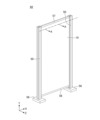
- Fig. 1 is a diagram showing an example of the configuration of an electromagnetic wave reflecting device 60 using a reflecting panel 10 of an embodiment.
- the electromagnetic wave reflecting device 60 has a reflecting panel 10 and a frame 50 that holds the reflecting panel 10.
- the width or horizontal direction of the reflecting panel 10 is the X direction
- the height or vertical direction is the Y direction
- the thickness direction is the Z direction.
- the reflecting panel 10 reflects electromagnetic waves from the gigahertz band to the terahertz band, such as microwaves, millimeter waves, and submillimeter waves, and reflects electromagnetic waves of, for example, 1 MHz to 300 GHz.
- the radio waves transmitted and received by the base station in a wireless transmission system including the electromagnetic wave reflecting device 60 are preferably, for example, radio waves in the frequency band of 1 MHz to 300 GHz, including the Sub-6 frequency band and millimeter wave band of the fifth generation mobile communication system (5G).
- 5G fifth generation mobile communication system
- the Sub-6 frequency band and the 28 GHz band included in the millimeter wave band are used, and the next-generation 6G mobile communication standard is expected to expand to the sub-terahertz band.
- the communication bandwidth can be significantly expanded, making it possible to communicate large amounts of data with low latency.
- the radio waves transmitted and received by the base station may be LTE (Long Term Evolution), LTE-A (LTE-Advanced), UMB (Ultra Mobile Broadband), or CBRS (Citizens Broadband Radio Service).
- the radio waves transmitted and received by the base station may be IEEE802.11 (Wi-Fi (registered trademark)), IEEE802.16 (WiMAX (registered trademark)), IEEE802.20, UWB (Ultra-Wideband), Bluetooth (registered trademark), or LPWA (Low Power Wide Area), etc.
- the reflective panel 10 may have a specular reflective surface in which the angles of incidence and emergence of the electromagnetic wave are equal, or may have a metasurface in which the reflection direction is controlled.
- the reflective panel 10 may be configured to combine a specular reflective surface and a metasurface.
- the metasurface may be designed not only to provide a non-specular reflective surface that reflects the incident electromagnetic wave in a direction different from the angle of incidence, but also to control the diffusion state of the electromagnetic wave.
- the metasurface of the reflective panel 10 reflects both horizontally polarized waves and vertically polarized waves in controlled directions.
- Horizontally polarized waves are waves that vibrate in a direction parallel to the ground or transverse to the direction of propagation.
- Vertically polarized waves are waves that vibrate in a direction perpendicular to the ground or longitudinal to the direction of propagation.
- the frame 50 holds two sides of the reflective panel 10 along the height direction when the reflective panel 10 is installed.
- a top frame 57 that holds the upper end of the reflective panel 10 and a bottom frame 58 that holds the lower end may be provided.
- the frame 50, the top frame 57, and the bottom frame 58 form a frame that holds the entire periphery of the reflective panel 10.
- the frame 50 may be called a "side frame” based on its positional relationship with the top frame 57 and the bottom frame 58.
- Legs 56 that support the frame 50 may be provided. As shown in FIG. 1, it is desirable to provide the legs 56 when the electromagnetic wave reflection device 60 is to be freestanding on the installation surface, but the legs 56 are not essential. Casters may be provided on the legs 56 to make it mobile, or the reflective panel 10 may be installed on a wall surface or hung from the ceiling without providing the legs 56.
- FIG. 2 is a diagram showing an example of the configuration of an electromagnetic wave reflecting fence 100 in which electromagnetic wave reflecting devices 60-1, 60-2, and 60-3 are connected.
- three electromagnetic wave reflecting devices 60-1, 60-2, and 60-3 (hereinafter, collectively referred to as “electromagnetic wave reflecting devices 60" as appropriate) are connected to form the electromagnetic wave reflecting fence 100, but there is no particular limit to the number of electromagnetic wave reflecting devices 60 that are connected.
- Electromagnetic wave reflection devices 60-1, 60-2, and 60-3 each have reflection panels 10-1, 10-2, and 10-3. Adjacent reflection panels are held together by a frame 50 to obtain an electromagnetic wave reflection fence 100 connected in the X direction.
- Each of reflection panels 10-1, 10-2, and 10-3 (hereinafter sometimes collectively referred to as "reflection panel 10") has, at least in part, a reflection surface formed of a hollow rectangular conductive pattern. This allows both horizontally polarized and vertically polarized radio waves to be reflected in a controlled direction.
- Fig. 3 is a diagram showing an example of the layer structure of the reflective panel 10.
- the layer structure shown in Fig. 3 is a layer structure in an XZ cross section of the reflective panel 10, and the stacking direction is the thickness direction (Z direction) of the reflective panel 10.
- Fig. 3 shows a cross section of the reflective panel 10 as seen from the bottom side (-Y direction side) as an example.
- the reflective panel 10 has a dielectric layer 11, a periodic conductive pattern 15 provided on one surface 11A of the dielectric layer 11, and a ground layer 12 provided on the other surface 11B of the dielectric layer 11.
- the conductive pattern 15 forms the reflective surface of the reflective panel 10, and reflects electromagnetic waves in the range of 1 MHz to 300 GHz in a predetermined direction.
- the conductive pattern 15 includes a periodic arrangement of a plurality of hollow patterns 151.
- the specific shape of the hollow patterns 151 will be described later with reference to FIG. 5.
- the hollow patterns are formed of, for example, good conductors such as Ag, Cu, Ni, and Al, and have a thickness of, for example, 0.01 mm to 0.05 mm. If the thickness is less than 0.01 mm, the surface resistivity becomes high, making it difficult to maintain high reflection efficiency. If the thickness is greater than 0.05 mm, it becomes difficult to maintain the flatness of the reflection surface.
- the surface of the conductive pattern 15 may be protected with a transparent film having a dielectric constant and dielectric tangent equivalent to those of the dielectric layer 11.
- the hollow pattern 151 is bonded to the dielectric layer 11 by an adhesive layer 13, for example.
- the adhesive layer 13 is not applied to the entire surface of the dielectric layer 11, but is applied in an amount necessary to stably support the hollow pattern 151. This is to minimize the effect of the adhesive layer 13 on the dielectric constant of the dielectric layer 11.
- the area occupied by the adhesive layer 13 does not need to be exactly the same as the area occupied by the conductive pattern 15, and may vary slightly within the range in which the hollow pattern 151 can be stably adhered to the dielectric layer 11. For example, if the area occupancy rate of the conductive pattern 15 relative to the dielectric layer 11 is 10.0% or more and 45.0% or less, the area occupancy rate of the adhesive layer 13 relative to the dielectric layer 11 is 9.0% or more and 50.0% or less.
- the area occupancy of the conductive pattern 15 is less than 10.0%, it becomes difficult to achieve the desired reflection characteristics and reflection efficiency. If the area occupancy of the conductive pattern 15 exceeds 45.0%, it becomes difficult to maintain the transparency of the reflective panel 10, but in applications where transparency is not required, the area occupancy of the conductive pattern 15 may be made greater than 45.0% to prioritize reflection efficiency.
- the adhesive layer 13 is a material capable of bonding the conductive pattern 15 to the dielectric layer 11, and may be, for example, a thermoplastic resin such as vinyl acetate resin, acrylic resin, cellulose resin, or silicone resin.
- the thickness of the adhesive layer 13 is a thickness capable of stably bonding the conductive pattern 15 to the dielectric layer 11, and is, for example, 0.002 mm or more and 0.050 mm or less. From the viewpoint of ensuring adhesive strength, it is desirable for the thickness to be 0.010 mm or more and 0.050 mm or less.
- the dielectric layer 11 is an insulating polymer film such as polycarbonate, cycloolefin polymer (COP), polyethylene terephthalate (PET), fluororesin, etc., and has a thickness of approximately 0.3 mm to 1.0 mm.
- the dielectric layer 11 may be any material that has a relative dielectric constant and dielectric tangent suitable for achieving the target reflection characteristics.
- the ground layer 12 may be formed of the same material as the conductive pattern 15, or may be formed of a different conductive material.
- the ground layer 12 forms a certain parasitic capacitance between the conductive pattern 15. The amount of phase delay is determined by the parasitic capacitance formed between the conductive pattern 15 and the ground layer 12.
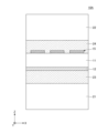
- FIG. 4 is a diagram showing an example of the layer structure of the reflective panel 10A.
- This layer structure has a configuration in which the layer structure of FIG. 3 is sandwiched between two dielectric substrates 21 and 22.
- the dielectric substrate 21 is bonded to the ground layer 12 by an adhesive layer 23.
- the dielectric substrate 22 is bonded to the conductive pattern 15 side of the dielectric layer 11 by an adhesive layer 24.
- the dielectric substrates 21 and 22 are transparent to electromagnetic waves from the gigahertz band to the terahertz band, specifically, electromagnetic waves from 1 MHz to 3 THz, for example, from 1 MHz to 300 GHz.
- the dielectric substrates 21 and 22 are preferably formed as the outermost layer of the reflective panel 10A from a material having excellent impact resistance, durability, and transparency.
- the dielectric substrates 21 and 22 can be made of polycarbonate, acrylic resin, PET, or the like.
- the thickness of the dielectric substrates 21 and 22 can be selected appropriately depending on the installation location, for example, between 1.0 mm and 10.0 mm.
- the thicknesses of the dielectric substrates 21 and 22 may be the same or different.
- the adhesive layer 23 protects the surface of the ground layer 12 and adheres and holds the dielectric substrate 21.
- the adhesive layer 24 protects the surface of the conductive pattern 15 and adheres and holds the dielectric substrate 22. It is desirable for the adhesive layers 23 and 24 to be durable and moisture resistant, and for example, ethylene-vinyl acetate (EVA) copolymer or cycloolefin polymer (COP) can be used.
- EVA ethylene-vinyl acetate
- COP cycloolefin polymer
- the thickness of the adhesive layers 23 and 24 is appropriately determined in the range of 10 ⁇ m to 400 ⁇ m so as to be able to join the dielectric substrates 21 and 22.
- the intrusion of moisture and air into the surface of the conductive pattern 15 is suppressed, and deterioration of the reflective surface is suppressed.
- the ground layer 12 By covering the ground layer 12 with an adhesive layer 23 and bonding the dielectric substrate 21, the intrusion of moisture and air into the surface of the ground layer 12 is suppressed, and surface deterioration of the ground layer 12 is suppressed. This keeps the capacitance between the ground layer 12 and the conductive pattern 15 constant, and makes it possible to maintain the magnitude of the designed phase delay. In other words, the reflection efficiency of radio waves in the designed direction can be maintained.
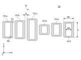
- FIG. 5 is a diagram showing an example of the configuration of a unit cell 20 of a conductive pattern 15 formed of a hollow pattern 151.
- the unit cell 20 has six hollow patterns 151a, 151b, 151c, 151d, 151e, and 151f.
- the width W1 and length L of the hollow patterns 151a to 151f correspond to the width (X) and height (Z) directions of the reflective panel 10 in FIG. 2A, respectively.
- the hollow patterns 151a to 151f have the same width W1 and different lengths L, but their central axes of length are aligned (the Y coordinate position of the central axis is constant).
- the pitch or spacing G in the X direction is constant.
- the shape and size of the hollow patterns 151a to 151f control the phase of reflection, and the reflected waves are superimposed to form a reflected beam in the desired direction.
- the unit cell 20 is designed to reflect the reflected wave beam of electromagnetic waves that are perpendicularly incident (incident angle 0°) in a direction 50° from the perpendicular.
- Hollow patterns 151a, 151b, 151c, 151d, 151e, and 151f have a hole of width W2.
- the hollow patterns have a rectangular ring shape when viewed in the XZ plane.
- the width of the vertical line segments is half the difference between the outer periphery width W1 and the inner periphery width W2 of each hollow pattern 151.
- the width of the horizontal line segments of hollow pattern 151 is determined according to the area of the hole.
- the vertical and horizontal line segments of hollow pattern 151 make it possible to reflect both vertically polarized and horizontally polarized radio waves.
- the corners of the inner circumference of the hollow pattern 151 are curved with a radius of curvature R2.
- the radius of curvature R1 is the same as or smaller than R2.
- the conductive pattern 15 is a periodic pattern in which unit cells 20 are repeatedly arranged in the X and Z directions.
- a reflective surface formed by the conductive pattern 15 on at least a portion of the reflective panel 10 it becomes possible to reflect both horizontally polarized and vertically polarized electromagnetic waves that are incident in a controlled direction.
- ⁇ Measuring equipment> 6 is a diagram showing an example of a measuring device arranged in the anechoic chamber 101.
- a VNA (Vector Network Analyzer) 110 is used as the measuring device.
- a transmitting antenna 115Tx and a receiving antenna 115Rx are connected to the VNA 110 via a cable 110A.
- the transmitting antenna 115Tx is directed toward the electromagnetic wave reflecting device 60, and the receiving antenna 115Rx is arranged in the reflecting direction of the electromagnetic wave reflecting device 60.
- a PC 120 is also connected to the VNA 110.
- the PC 120 may be located inside the anechoic chamber 101, but in FIG. 6 it is located outside the anechoic chamber 101 as an example.
- the electromagnetic wave reflection device 60, the transmitting antenna 115Tx, and the receiving antenna 115Rx are placed at a predetermined height above the floor surface in the anechoic chamber 101 using a tripod or the like.
- the relative positions of the transmitting antenna 115Tx and the receiving antenna 115Rx are fixed.
- the position of the electromagnetic wave reflection device 60 with respect to the transmitting antenna 115Tx and the receiving antenna 115Rx is also fixed.
- the angle of the electromagnetic wave reflecting device 60 may be changed while fixing the transmitting antenna 115Tx and the receiving antenna 115Rx, or the angle of the electromagnetic wave reflecting device 60 may be fixed while changing the position (orientation) of the transmitting antenna 115Tx and the receiving antenna 115Rx. Also, the positions (orientations) of both the electromagnetic wave reflecting device 60 and the transmitting antenna 115Tx and the receiving antenna 115Rx may be changed.
- the VNA 110 includes a transmission circuit section that transmits a transmission signal to a transmission antenna 115Tx, and a reception circuit section that measures the power (reception power) of a reception signal received by a reception antenna 115Rx, as well as a processing section 111 and a memory 112.
- the transmission circuit section and reception circuit section of the VNA 110 are omitted in FIG.
- VNA 110 may also be separated into a VNA connected to the transmitting antenna 115Tx and a VNA connected to the receiving antenna 115Rx, and the two VNAs may be connected by an optical cable or the like to operate in cooperation with each other.
- the VNA 110 incorporates a computer system that realizes the processing unit 111 and memory 112.
- the computer system is realized by a computer including a CPU (Central Processing Unit), RAM (Random Access Memory), ROM (Read Only Memory), an input/output interface, and an internal bus.
- the processing unit 111 represents the functions of the programs executed by the computer system of the VNA 110 as functional blocks.
- the memory 112 is a functional representation of the memory of the computer system of the VNA 110.
- the processing unit 111 controls the transmission circuit unit and the reception circuit unit of the VNA 110 to perform a process of emitting radio waves from the transmission antenna 115Tx and a process of measuring the reception power of the radio waves received by the reception antenna 115Rx. This process is realized by the reception power measurement method of the embodiment.
- the processing unit 111 controls the transmitting circuit unit to transmit radio waves of a predetermined band selected from a frequency band of 1 MHz to 300 GHz from the transmitting antenna 115Tx.
- the selection of the predetermined band is performed by the operator of the PC 120 inputting the desired band to the PC 120, which then transmits data representing the predetermined band to the VNA 110. Note that the selection of the predetermined band may be performed directly on the VNA 110 without going through the PC 120.
- the processing unit 111 controls the receiving circuit unit to scan the frequency of the received power within a specified frequency range and measures the received power at the electromagnetic wave reflection device 60. By using the time domain function, the processing unit 111 can distinguish between the reflected wave at the electromagnetic wave reflection device 60, the reflected wave at the inner wall of the anechoic chamber 101, and the direct wave.
- the reflected wave at the electromagnetic wave reflecting device 60 is a radio wave that is transmitted from the transmitting antenna 115Tx, reflected by the electromagnetic wave reflecting device 60, and reaches the receiving antenna 115Rx.
- the reflected wave at the inner wall of the anechoic chamber 101 is a radio wave that is transmitted from the transmitting antenna 115Tx, reflected by the inner wall of the anechoic chamber 101, and reaches the receiving antenna 115Rx.
- the direct wave is a radio wave that is transmitted from the transmitting antenna 115Tx, and reaches the receiving antenna 115Rx directly.
- the power reflection coefficient is calculated based on the received power, but this processing may be performed by either the processing unit 111 of the VNA 110 or the processing unit 121 of the PC 120, or may be shared between the processing units 111 and 121.
- this processing may be performed by either the processing unit 111 of the VNA 110 or the processing unit 121 of the PC 120, or may be shared between the processing units 111 and 121.
- a form in which the processing unit 111 of the VNA 110 calculates the power reflection coefficient based on the received power is described. That is, here, as an example, a form in which the processing unit 111 of the VNA 110 executes the calculation processing according to the method of calculating the power reflection efficiency is described. Details of the method of calculating the power reflection efficiency will be described later with reference to Figures 6 to 8.
- the memory 112 stores programs, data, and the like required for the processing unit 111 of the VNA 110 to execute the calculation process according to the method for calculating the power reflection efficiency.
- the PC 120 incorporates a computer system that realizes a processing unit 121 and a memory 122.
- the computer system is realized by a computer including a CPU, RAM, ROM, an input/output interface, an internal bus, etc.
- the processing unit 121 is a functional block showing the functions of a program executed by the computer system of the PC 120.
- the memory 122 is a functional representation of the memory of the computer system of the PC 120.
- the processing unit 111 of the VNA 110 executes the calculation process using the power reflection efficiency calculation method.
- the processing unit 121 of the PC 120 may execute the calculation process using the power reflection efficiency calculation method, or the processing units 111 and 121 may share the task of executing the calculation process using the power reflection efficiency calculation method.
- the memory 122 stores programs, data, etc. required for the processing unit 121 to execute the processing.
- ⁇ Calculation method of power reflection efficiency according to the embodiment> 7A and 7B are diagrams for explaining an example of a method for calculating the power reflection efficiency according to the embodiment, and show the XYZ coordinate system common to FIGS.
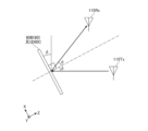
- Figures 7A and 7B show a simplified positional relationship between the transmitting antenna 115Tx, the receiving antenna 115Rx, and the electromagnetic wave reflecting device 60 on a two-dimensional plane.
- the electromagnetic wave reflecting device 60 having a metasurface may be referred to as the electromagnetic wave reflecting device 60A
- the electromagnetic wave reflecting device 60 having a regular reflecting surface may be referred to as the electromagnetic wave reflecting device 60B.
- the electromagnetic wave reflecting devices 60A and 60B they will simply be referred to as the electromagnetic wave reflecting device 60.
- the electromagnetic wave reflecting device 60C is an example of a reflector having a metal reflecting surface.
- the electromagnetic wave reflecting device 60C only needs to have a flat metal surface as its reflecting surface, and as an example, an aluminum metal plate can be used as the electromagnetic wave reflecting device 60C. Note that since the reflecting surface only needs to be a flat metal surface, a reflector in which aluminum foil is attached to a resin substrate or the like can also be used as the electromagnetic wave reflecting device 60C.
- FIG. 7A shows an electromagnetic wave reflection device 60A with a metasurface
- FIG. 7B shows an electromagnetic wave reflection device 60B with a regular reflection surface
- electromagnetic wave reflection device 60C which is made of a perfect conductor, performs specular reflection in the same way as electromagnetic wave reflection device 60B, and is therefore referred to as electromagnetic wave reflection device 60B (60) or 60C in FIG. 7B.
- the angles and distances of the electromagnetic wave reflecting device 60A, the transmitting antenna 115Tx, and the receiving antenna 115Rx are set in advance so that, as an example, the transmitting antenna 115Tx is located in the direction of an incident angle of 0 degrees on the electromagnetic wave reflecting device 60A, and the receiving antenna 115Rx is located in the direction of a reflection angle of ⁇ degrees when a radio wave is incident with an incident angle of 0 degrees.
- the angle ⁇ is the angle formed by the transmitting antenna 115Tx and the receiving antenna 115Rx with respect to the electromagnetic wave reflecting device 60A.
- the normal to the reflecting surface is shown by a dashed line.
- the distance between the electromagnetic wave reflecting device 60A and the transmitting antenna 115Tx on the path of the incident wave is equal to the distance between the electromagnetic wave reflecting device 60A and the receiving antenna 115Rx on the path of the reflected wave.
- the normal to the reflecting surface of the electromagnetic wave reflecting device 60A faces the horizontal direction.
- the incident angle does not have to be 0 degrees.
- the electromagnetic wave reflecting device 60A reflects the radio wave in a direction shifted by ⁇ degrees from the incident angle.
- the positions of the transmitting antenna 115Tx and the receiving antenna 115Rx are not changed, and the angle of the electromagnetic wave reflecting device 60C is adjusted so that the direction of the normal to the reflecting surface of the electromagnetic wave reflecting device 60C passes through the center of the angle ⁇ in FIG. 7A.
- the angle 2 ⁇ is the angle that the transmitting antenna 115Tx and the receiving antenna 115Rx make with respect to the electromagnetic wave reflecting device 60C.
- the distance between the electromagnetic wave reflecting device 60A and the transmitting antenna 115Tx on the path of the incident wave is equal to the distance between the electromagnetic wave reflecting device 60A and the receiving antenna 115Rx on the path of the reflected wave.
- the same reflection conditions mean that the angle ⁇ in FIG. 7A is the same as the sum (2 ⁇ ) of the incident angle ⁇ and the reflection angle ⁇ in FIG. 7B, and that the distance between the electromagnetic wave reflecting device 60A in FIG. 7A and the transmitting antenna 115Tx and the receiving antenna 115Rx is equal to the distance between the electromagnetic wave reflecting device 60C in FIG. 7B and the transmitting antenna 115Tx and the receiving antenna 115Rx.
- the received power P1 of the reflected wave reflected by the electromagnetic wave reflecting device 60A and the received power P2 of the reflected wave reflected by the electromagnetic wave reflecting device 60C are measured, and the power reflection coefficient ⁇ 1 is calculated from the received power P1, and the power reflection coefficient ⁇ 2 is calculated from the received power P2.
- the power reflection efficiency H of the electromagnetic wave reflecting device 60A is calculated by dividing the power reflection coefficient ⁇ 1 by the power reflection coefficient ⁇ 2. In this way, the power reflection efficiency H of the electromagnetic wave reflecting device 60A is calculated by normalizing the power reflection coefficient ⁇ 1 of the electromagnetic wave reflecting device 60A by the power reflection coefficient ⁇ 2 of the electromagnetic wave reflecting device 60C, which is composed of a perfect conductor.
- the power reflection efficiency H of the electromagnetic wave reflection device 60A with a metasurface is the value obtained by dividing ⁇ 1/ ⁇ 2 by the correction value.
- the correction value ⁇ p can be expressed as
- E MR /E PEC is expressed by the following formula (1) or (2).
- ⁇ is the angle of incidence on the metasurface
- Fig. 8 is a flowchart showing an example of the process of the method for measuring received power and the method for calculating power reflection efficiency according to the embodiment.
- the processing unit 111 of the VNA 110 executes the process shown in Fig. 8.
- the process shown in Fig. 8 is executed by the processing unit 111 executing a program for measuring received power and a program for calculating power reflection efficiency that realize the method for measuring received power and the method for calculating power reflection efficiency.
- the processing unit 111 controls the transmission circuit unit to transmit radio waves in a predetermined band selected from a frequency band of 1 MHz to 300 GHz from the transmitting antenna 115Tx, and causes the radio waves to be incident on the electromagnetic wave reflecting device 60 (60A or 60B) at a first specified incident angle (step S1).
- the first specified incident angle is, for example, 0 degrees in the case of the electromagnetic wave reflecting device 60A, and is an incident angle ( ⁇ ) determined by the positional relationship between the transmitting antenna 115Tx and the receiving antenna 115Rx in the case of the electromagnetic wave reflecting device 60B.
- the incident angle determined by the positional relationship between the transmitting antenna 115Tx and the receiving antenna 115Rx is an angle specified by the design of the electromagnetic wave reflecting device 60B.
- Step S1 is an example of process 1.
- the receiving antenna 115Rx arranged in the direction of the first specified reflection angle relative to the electromagnetic wave reflecting device 60 (60A or 60B), receives the reflected wave of the radio wave incident on the electromagnetic wave reflecting device 60 (60A or 60B) in the first step, and the processing unit 111 measures the received power P1 in the specified frequency range (step S2).
- Step S2 is an example of step 2.
- the received power P1 is an example of the first received power.
- the first specified reflection angle is the reflection angle ⁇ specified by the design of the electromagnetic wave reflecting device 60A, and in the case of the electromagnetic wave reflecting device 60B, it is an angle equal to the incident angle in step S1.
- the specified frequency range is a frequency band including multiple measurement points using the time domain function, and can be set in the VNA 110.
- the specified band selected from the frequency band of 1 MHz to 300 GHz is 28 GHz
- the specified frequency range is 22 GHz to 40 GHz
- the multiple measurement points are multiple frequencies set at 10 MHz intervals within the range from 22 GHz to 40 GHz.
- the processing unit 111 controls the transmission circuit unit to transmit radio waves in the same predetermined band as in step S1 from the transmission antenna 115Tx, and makes the radio waves incident on the electromagnetic wave reflecting device 60C at a second specified angle of incidence (step S3). If the electromagnetic wave reflecting device 60A is used in step S1, the second specified angle of incidence is half the reflection angle ⁇ specified by the design of the electromagnetic wave reflecting device 60A, and if the electromagnetic wave reflecting device 60B is used in step S1, the second specified angle of incidence is equal to the first specified angle of incidence for the electromagnetic wave reflecting device 60B in step S1.
- Step S3 is an example of process 1.
- the receiving antenna 115Rx which is arranged in the direction of the second designated reflection angle with respect to the electromagnetic wave reflecting device 60C, receives the reflected wave of the radio wave incident on the electromagnetic wave reflecting device 60C in the third step, and the processing unit 111 measures the received power P2 in the designated frequency range (step S4).
- Step S4 is an example of step 4.
- the received power P2 is an example of the second received power. If the electromagnetic wave reflecting device 60A is used in step S2, the second designated reflection angle is an angle that is half the reflection angle ⁇ of the electromagnetic wave reflecting device 60A, and if the electromagnetic wave reflecting device 60B is used in step S2, the second designated reflection angle is an angle equal to the first designated reflection angle for the electromagnetic wave reflecting device 60B in step S2.
- steps S1 to S4 may be performed first, followed by the processing of steps S1 and S2.
- the position of the electromagnetic wave reflecting device 60 (60A or 60B) in steps S1 and S2 relative to the transmitting antenna 115Tx and the receiving antenna 115Rx is equal to the position of the electromagnetic wave reflecting device 60C in steps S3 and S4 relative to the transmitting antenna 115Tx and the receiving antenna 115Rx.
- the positions of the electromagnetic wave reflecting devices 60A and 60B in steps S1 and S2 are, as an example, the center of gravity positions of the electromagnetic wave reflecting devices 60A and 60B.
- the processing unit 111 calculates the power reflection coefficient ⁇ 1 of the electromagnetic wave reflecting device 60 (60A or 60B) and the power reflection coefficient ⁇ 2 of the electromagnetic wave reflecting device 60C based on the received powers P1 and P2 (step S5).
- the power reflection coefficient ⁇ 1 is calculated as a reflection coefficient of the S-parameter based on the received power P1
- the power reflection coefficient ⁇ 2 is calculated as a reflection coefficient of the S-parameter based on the received power P2.
- Step S5 is an example of the fifth step.
- the power reflection coefficient ⁇ 1 is an example of a first power reflection coefficient
- the power reflection coefficient ⁇ 2 is an example of a second power reflection coefficient.
- the processing unit 111 calculates the power reflection efficiency H of the electromagnetic wave reflection device 60 (60A or 60B) by dividing the power reflection coefficient ⁇ 1 by the power reflection coefficient ⁇ 2 (step S6).
- Step S6 is an example of the sixth step.
- the power reflection efficiency H is calculated as ⁇ 1/ ⁇ 2.
- processing unit 111 executes step S7.
- Step S7 is an example of the seventh step.
- the processing unit 111 then ends the series of processes (end).
- Example 1 is Example 1.
- An anechoic chamber 101 having a length of 5.0 m, a width of 5.0 m, and a height of 3.0 m was used.
- a high-frequency signal at a designated frequency of 22.0 GHz to 40.0 GHz was output from the VNA 110 inside the anechoic chamber 101, and propagated through space via the transmitting antenna 115Tx, incident at an angle of +25° on an aluminum plate having a thickness of 5.0 mm as an electromagnetic wave reflection device 60C composed of a perfect conductor, and the reflected wave was received by the receiving antenna 115Rx in a direction of -25°.
- the received power P2 at 28.0 GHz was measured at the terminal of the VNA 110 connected to the receiving antenna 115Rx.
- the size of the aluminum plate (length in the X direction x length in the Y direction) was 0.2 m x 0.2 m, the distance from the transmitting antenna 115Tx to the aluminum plate on the path of the incident wave was 1.5 m, and the distance from the aluminum plate to the receiving antenna 115Rx on the path of the reflected wave was 1.5 m.
- the received power P2 was ⁇ 29.7 dB, and the power reflection coefficient ⁇ 2 was 0.00108.
- the electromagnetic wave was incident at an angle of +25° on the electromagnetic wave reflection device 60B having a regular reflection surface of 5.0 mm in thickness by spatial propagation through the transmitting antenna 115Tx, and the reflected wave was received at a direction of -25° by the receiving antenna 115Rx, and the received power P1 at 28.0 GHz was measured at the terminal of the VNA 110 connected to the receiving antenna 115Rx.
- the size of the electromagnetic wave reflection device 60B (length in the X direction x length in the Y direction) was 0.2 m x 0.2 m, the distance from the transmitting antenna 115Tx to the electromagnetic wave reflection device 60B on the path of the incident wave was 1.5 m, and the distance from the electromagnetic wave reflection device 60B to the receiving antenna 115Rx on the path of the reflected wave was 1.5 m.
- the received power P1 was -29.8 dB, and the power reflection coefficient ⁇ 1 was 0.00105.
- the ratio of ⁇ 1/ ⁇ 2 was 98.1%. This was consistent with the results of the electromagnetic field analysis performed in advance.
- Example 2 is Example 2.
- An anechoic chamber 101 having a length of 5.0 m, a width of 5.0 m, and a height of 3.0 m was used.
- a high-frequency signal at a designated frequency of 22.0 GHz to 40.0 GHz was output from the VNA 110 inside the anechoic chamber 101, and propagated through space via the transmitting antenna 115Tx, incident at an angle of +25° on an aluminum plate having a thickness of 5.0 mm as an electromagnetic wave reflection device 60C composed of a perfect conductor, and the reflected wave was received by the receiving antenna 115Rx in a direction of -25°.
- the received power P2 at 28.0 GHz was measured at the terminal of the VNA 110 connected to the receiving antenna 115Rx.
- the size of the aluminum plate (length in the X direction x length in the Y direction) was 0.2 m x 0.2 m, the distance from the transmitting antenna 115Tx to the aluminum plate on the path of the incident wave was 1.5 m, and the distance from the aluminum plate to the receiving antenna 115Rx on the path of the reflected wave was 1.5 m.
- the received power P2 was ⁇ 29.7 dB, and the power reflection coefficient ⁇ 2 was 0.00108.
- radio waves were incident on the electromagnetic wave reflecting device 60A having a metasurface with a thickness of 5.0 mm by spatial propagation through the transmitting antenna 115Tx at an incident angle of 0°, and the reflected wave was received by the receiving antenna 115Rx in a direction of +50°, and the received power at 28.0 GHz was measured at the terminal of the VNA 110 connected to the receiving antenna 115Rx.
- the size (length in the X direction x length in the Y direction) of the electromagnetic wave reflecting device 60A was 0.2 m x 0.2 m, the distance from the transmitting antenna 115Tx to the electromagnetic wave reflecting device on the path of the incident wave was 1.5 m, and the distance from the electromagnetic wave reflecting device to the receiving antenna 115Rx on the path of the reflected wave was 1.5 m.
- the received power P1 was -30.8 dB, and the power reflection coefficient ⁇ 1 was 0.00082.
- the ratio of ⁇ 1/ ⁇ 2 was 75.9%.
- the correction value was 0.96, so the power reflection efficiency after correction was 79.1%, which was consistent with the results of the electromagnetic field analysis performed in advance.
- Example 3 is Example 3.
- a radio wave anechoic chamber 101 having a length of 5.0 m, a width of 5.0 m, and a height of 3.0 m was used.
- a high-frequency signal at a designated frequency of 22.0 GHz to 40.0 GHz was output from the VNA 110 inside the radio wave anechoic chamber 101, and propagated through space via the transmitting antenna 115Tx, incident at an angle of +15° on an aluminum plate having a thickness of 5.0 mm as an electromagnetic wave reflection device 60C composed of a perfect conductor, and the reflected wave was received by the receiving antenna 115Rx in a direction of -15°.
- the received power P2 at 28.0 GHz was measured at the terminal of the VNA 110 connected to the receiving antenna 115Rx.
- the size of the aluminum plate (length in the X direction x length in the Y direction) was 0.3 m x 0.3 m, the distance from the transmitting antenna 115Tx to the aluminum plate on the path of the incident wave was 3.0 m, and the distance from the aluminum plate to the receiving antenna 115Rx on the path of the reflected wave was 3.0 m.
- the received power P2 was ⁇ 29.7 dB, and the power reflection coefficient ⁇ 2 was 0.00108.
- radio waves were incident on the electromagnetic wave reflecting device 60A having a metasurface with a thickness of 5.0 mm by spatial propagation through the transmitting antenna 115Tx at an incident angle of 0°, and the reflected wave was received by the receiving antenna 115Rx in a direction of +30°, and the received power P1 at 28.0 GHz was measured at the terminal of the VNA 110 connected to the receiving antenna 115Rx.
- the size (length in the X direction x length in the Y direction) of the electromagnetic wave reflecting device 60A was 0.3 m x 0.3 m, the distance from the transmitting antenna 115Tx to the electromagnetic wave reflecting device 60A on the path of the incident wave was 1.5 m, and the distance from the electromagnetic wave reflecting device 60A to the receiving antenna 115Rx on the path of the reflected wave was 1.5 m.
- the received power P1 was -30.2 dB, and the power reflection coefficient ⁇ 1 was 0.00095.
- the ratio of ⁇ 1/ ⁇ 2 was 88.0%.
- the correction value was 0.98, so the power reflection efficiency after correction was 89.8%, which was consistent with the results of the electromagnetic field analysis performed in advance.
- Example 4 is Example 4.
- a radio wave anechoic chamber 101 having a length of 5.0 m, a width of 5.0 m, and a height of 3.0 m was used.
- a high-frequency signal at a designated frequency of 22.0 GHz to 40.0 GHz was output from the VNA 110 inside the radio wave anechoic chamber 101, and propagated through space via the transmitting antenna 115Tx, incident at an angle of +15° on an aluminum plate having a thickness of 5.0 mm as an electromagnetic wave reflection device 60C composed of a perfect conductor, and the reflected wave was received by the receiving antenna 115Rx in a direction of -15°.
- the received power at 28.0 GHz was measured at the terminal of the VNA 110 connected to the receiving antenna 115Rx.
- the size of the aluminum plate (length in the X direction x length in the Y direction) was 0.5 m x 0.2 m, the distance from the transmitting antenna 115Tx to the aluminum plate on the path of the incident wave was 8.0 m, and the distance from the aluminum plate to the receiving antenna 115Rx on the path of the reflected wave was 8.0 m.
- the received power P2 was ⁇ 29.7 dB, and the power reflection coefficient ⁇ 2 was 0.00108.
- radio waves were incident on the electromagnetic wave reflecting device 60A having a metasurface with a thickness of 5.0 mm by spatial propagation through the transmitting antenna 115Tx at an incident angle of 0°, and the reflected wave was received by the receiving antenna 115Rx in a direction of +45°, and the received power at 28.0 GHz was measured at the terminal of the VNA 110 connected to the receiving antenna 115Rx.
- the size (length in the X direction x length in the Y direction) of the electromagnetic wave reflecting device 60A was 0.2 m x 0.2 m, the distance from the transmitting antenna 115Tx to the electromagnetic wave reflecting device 60A on the path of the incident wave was 1.5 m, and the distance from the electromagnetic wave reflecting device 60A to the receiving antenna 115Rx on the path of the reflected wave was 1.5 m.
- the received power P1 was -30.5 dB, and the power reflection coefficient ⁇ 1 was 0.00089.
- the ratio of ⁇ 1/ ⁇ 2 was 82.4%, but the correction value was 0.99, so the power reflection efficiency after correction was 83.2%, which was consistent with the results of the electromagnetic field analysis performed in advance.
- Example 5 is Comparative Example 1.
- a radio wave anechoic chamber 101 having a length of 5.0 m, a width of 5.0 m, and a height of 3.0 m was used.
- a high-frequency signal at a designated frequency of 22.0 GHz to 40.0 GHz was output from the VNA 110 inside the radio wave anechoic chamber 101, and propagated through space via the transmitting antenna 115Tx, incident at an angle of +25.0° on an aluminum plate having a thickness of 5.0 mm as an electromagnetic wave reflection device 60C composed of a perfect conductor, and the reflected wave was received by the receiving antenna 115Rx in a direction of -25.0°, and the received power at 28.0 GHz was measured at the terminal of the VNA 110 connected to the receiving antenna 115Rx.
- the size of the aluminum plate (length in the X direction x length in the Y direction) was 0.3 m x 0.3 m, the distance from the transmitting antenna 115Tx to the aluminum plate on the path of the incident wave was 1.0 m, and the distance from the aluminum plate to the receiving antenna 115Rx on the path of the reflected wave was 1.0 m.
- the received power was ⁇ 29.5 dB, and the power reflection coefficient ⁇ 2 was 0.00112.
- radio waves were incident at an incidence angle of 0° on the electromagnetic wave reflecting device 60A having a metasurface with a thickness of 5.0 mm by spatial propagation through the transmitting antenna 115Tx, and the reflected wave was received by the receiving antenna 115Rx in a direction of +50°.
- the received power at 28.0 GHz was measured at the terminal of the VNA 110 connected to the receiving antenna 115Rx.
- the size of the electromagnetic wave reflecting device (length in the X direction x length in the Y direction) was 0.3 m x 0.3 m, the distance from the transmitting antenna 115Tx to the electromagnetic wave reflecting device on the path of the incident wave was 0.3 m, and the distance from the electromagnetic wave reflecting device to the receiving antenna 115Rx on the path of the reflected wave was 0.3 m.
- the received power was -30.5 dB, and the power reflection coefficient was 0.00089 ( ⁇ 2).
- the ratio of ⁇ 1/ ⁇ 2 was 63.4%, but the correction value was 2.12, which exceeds 1 and cannot be corrected. Furthermore, the results did not match those of the electromagnetic field analysis conducted in advance.
- Example 6 is Comparative Example 2.
- An anechoic chamber 101 having a length of 5.0 m, a width of 5.0 m, and a height of 3.0 m was used.
- a high-frequency signal at a designated frequency of 22.0 GHz to 40.0 GHz was output from the VNA 110 inside the anechoic chamber 101, and propagated through space via the transmitting antenna 115Tx to an aluminum plate having a thickness of 5.0 mm as an electromagnetic wave reflection device 60C composed of a perfect conductor at an angle of +25°.
- the reflected wave was received by the receiving antenna 115Rx in a direction of -25°, and the received power at 28.0 GHz was measured at the terminal of the VNA 110 connected to the receiving antenna 115Rx.
- the size of the aluminum plate (length in the X direction x length in the Y direction) was 0.5 m x 0.2 m, the distance from the transmitting antenna 115Tx to the aluminum plate on the path of the incident wave was 2.9 m, and the distance from the aluminum plate to the receiving antenna 115Rx on the path of the reflected wave was 2.9 m.
- the received power was ⁇ 29.5 dB, and the power reflection coefficient ⁇ 2 was 0.00112.
- radio waves were incident on the electromagnetic wave reflecting device 60A having a metasurface with a thickness of 5.0 mm by spatial propagation through the transmitting antenna 115Tx at an incident angle of 0°, and the reflected wave was received by the receiving antenna 115Rx in a direction of +50°, and the received power at 28.0 GHz was measured at the terminal of the VNA 110 connected to the receiving antenna 115Rx.
- the size (length in the X direction x length in the Y direction) of the electromagnetic wave reflecting device 60A was 0.3 m x 0.3 m
- the distance from the transmitting antenna 115Tx to the electromagnetic wave reflecting device 60A on the path of the incident wave was 0.3 m
- the distance from the electromagnetic wave reflecting device 60A to the receiving antenna 115Rx on the path of the reflected wave was 0.3 m.
- the received power P1 was -30.9 dB
- the power reflection coefficient ⁇ 1 was 0.00081.
- the ratio of ⁇ 1/ ⁇ 2 was 72.3%, and the correction value was 2.12, which exceeded 1 and made it impossible to correct. In addition, it did not match the results of the electromagnetic field analysis that was performed in advance.
- Example 7 is Comparative Example 3.
- a radio wave anechoic chamber 101 having a length of 5.0 m, a width of 5.0 m, and a height of 3.0 m was used.
- a high-frequency signal at a designated frequency of 22.0 GHz to 40.0 GHz was output from the VNA 110 inside the radio wave anechoic chamber 101, and propagated through space via the transmitting antenna 115Tx, incident at an angle of +30° on an aluminum plate having a thickness of 5.0 mm as an electromagnetic wave reflection device 60C composed of a perfect conductor, and the reflected wave was received by the receiving antenna 115Rx in a direction of -30°.
- the received power at 28.0 GHz was measured at the terminal of the VNA 110 connected to the receiving antenna 115Rx.
- the size of the aluminum plate (length in the X direction x length in the Y direction) was 0.5 m x 0.2 m, the distance from the transmitting antenna 115Tx to the aluminum plate on the path of the incident wave was 2.0 m, and the distance from the aluminum plate to the receiving antenna 115Rx on the path of the reflected wave was 2.0 m.
- the received power P2 was ⁇ 29.5 dB, and the power reflection coefficient ⁇ 2 was 0.00112.
- radio waves were incident on the electromagnetic wave reflecting device 60A having a metasurface with a thickness of 5.0 mm by spatial propagation through the transmitting antenna 115Tx at an incident angle of 0°, and the reflected wave was received by the receiving antenna 115Rx in a direction of +60°, and the received power at 28.0 GHz was measured at the terminal of the VNA 110 connected to the receiving antenna 115Rx.
- the size of the electromagnetic wave reflecting device 60A (length in the X direction x length in the Y direction) was 0.5 m x 0.2 m, the distance from the transmitting antenna 115Tx to the electromagnetic wave reflecting device 60A on the path of the incident wave was 0.3 m, and the distance from the electromagnetic wave reflecting device 60A to the receiving antenna 115Rx on the path of the reflected wave was 0.3 m.
- the received power was -30.5 dB, and the power reflection coefficient ⁇ 1 was 0.00089.
- the ratio of ⁇ 1/ ⁇ 2 was 63.4%, and the correction value was 2.02, which exceeded 1 and made it impossible to correct. In addition, it did not match the results of the electromagnetic field analysis that was performed in advance.
- FIGS. 9A and 9B are diagrams showing an example of the measurement results of the distance from the transmitting antenna 115Tx to the electromagnetic wave reflecting device 60A on the path of the incident wave and the distance from the electromagnetic wave reflecting device 60A to the receiving antenna 115Rx on the path of the reflected wave when the correction value is 1 or less and a slight deviation in the measurement distance does not result in a large change. "No large change" means that the deviation in the measurement distance is to the extent that does not cause practical problems in calculating the power reflection efficiency.
- FIG. 9C is a diagram showing an example of the configuration of the reflecting surface of the electromagnetic wave reflecting device 60A.
- the rectangular reflecting surface of the electromagnetic wave reflecting device 60A has a length (width) of X (m) in the X direction and a length of Y (m) in the Y direction.
- the transmitting antenna 115Tx is located in the direction of the electromagnetic wave reflecting device 60A with an incident angle of 0 degrees
- the receiving antenna 115Rx is located in the direction of the reflection angle of ⁇ degrees when the radio wave is incident with an incident angle of 0 degrees.
- the reflection angle ⁇ takes a positive value in the direction indicated by the arrow in Figure 9C, and a negative value in the opposite direction.
- Figure 9A shows an example of the measurement result of the distance L (see Figure 9C) between the electromagnetic wave reflecting device 60A and the transmitting antenna 115Tx and receiving antenna 115Rx when the electromagnetic wave reflecting device 60A has the same length in the X and Y directions, the correction value is 1 or less, and even if the measurement distance is slightly deviated, there is no significant change.
- the distance L is the measurement result of the distance from the transmitting antenna 115Tx to the electromagnetic wave reflecting device 60A on the path of the incident wave, and the distance from the electromagnetic wave reflecting device 60A to the receiving antenna 115Rx on the path of the reflected wave, when the correction value is 1 or less, and even if the measurement distance is slightly deviated, there is no significant change.
- the distance L is 2.85 m or more.
- the correction value is greater than 1, and even a slight deviation in the measured distance, taking into account the installation and angle accuracy of the antenna and sample, can result in a correction value that is much smaller than the actual appropriate correction value.
- the distance L is 2.85 m or more, the correction value is 1 or less, and even a slight deviation in the measured distance does not result in a large change.
- the distance L increased from 2.85 m to 31.5 m.
- the correction value was greater than 1, and even a slight deviation in the measured distance could result in a correction value that was much smaller than the actual appropriate correction value.
- the distance L was 31.5 m or more, the correction value was less than 1, and even a slight deviation in the measured distance did not result in a large change.
- FIG. 9B shows an example of the measurement results of the distance L between the electromagnetic wave reflection device 60A and the transmitting antenna 115Tx and receiving antenna 115Rx when the lengths in the X direction and Y direction of the electromagnetic wave reflection device 60A are the same or not, the correction value is 1 or less, and even if the measurement distance is slightly shifted, there is no large change.
- the correction value is 1 or less, and even if the measurement distance is slightly deviated, the distance L between the electromagnetic wave reflection device 60A and the transmitting antenna 115Tx and the receiving antenna 115Rx is 1.3 m.
- the distance L is less than 1.30 m, the correction value is greater than 1, and even if the measurement distance is deviated even slightly, the correction value can be much smaller than the actual appropriate correction value.
- the distance L is 1.30 m or more, the correction value is 1 or less, and even if the measurement distance is deviated slightly, the correction value does not change significantly.
- the distance L is about four times longer than the distance L when the electromagnetic wave reflection device 60A has a length of 0.2 m in the X direction and a length of 0.4 m in the Y direction.
- the electromagnetic wave reflection device 60A has a length of 0.2 m in the X direction and a length of 0.2 m in the Y direction
- the distance L is less than 1.30 m
- the correction value is greater than 1, and even a slight deviation in the measured distance can result in a correction value that is much smaller than the actual appropriate correction value.
- the distance L is 1.30 m or more
- the correction value is 1 or less, and even a slight deviation in the measured distance does not result in a large change.
- the distance L in this case is the same as the distance L when the electromagnetic wave reflection device 60A has a length of 0.2 m in the X direction and a length of 0.4 m in the Y direction.
- the electromagnetic wave reflection device 60A has a length of 0.4 m in the X direction and a length of 0.4 m in the Y direction
- the distance L is less than 5.00 m
- the correction value is greater than 1, and even a slight deviation in the measured distance can result in a correction value that is much smaller than the actual appropriate correction value.
- the distance L is 5.00 m or more
- the correction value is less than 1, and even a slight deviation in the measured distance does not result in a large change.
- the distance L in this case is the same as the distance L when the electromagnetic wave reflection device 60A has a length of 0.4 m in the X direction and a length of 0.2 m in the Y direction.
- FIG. 10 is a diagram showing an example of the results of fitting a quadratic curve to the results of FIG. 9A.
- the horizontal axis shows the length (m) of the electromagnetic wave reflection device 60A in the X and Y directions.
- the vertical axis shows the distance L.
- the fitted quadratic curve can be expressed by the following equation (3).
- the method of measuring the received power includes a first step (step S1) of transmitting radio waves in a predetermined band selected from a frequency band of 1 MHz to 300 GHz from the transmitting antenna 115Tx inside an anechoic chamber 101 in which a VNA 110 connected to a transmitting antenna 115Tx and a receiving antenna 115Rx whose relative positions are fixed is arranged, and making the radio waves incident on an electromagnetic wave reflecting device 60 (60A or 60B) at a first designated incident angle, and a second step (step S2) of measuring the reflected wave of the radio waves incident on the electromagnetic wave reflecting device 60 (60A or 60B) in the first step by using a receiving antenna 115Rx arranged in a direction of the first designated reflection angle with respect to the electromagnetic wave reflecting device 60 (60A or 60B).
- the method includes a second step (step S2) of receiving the electromagnetic wave and measuring the first reception power in a specified frequency range with the VNA 110, a third step (step S3) of transmitting radio waves in a specified band from the transmitting antenna 115Tx inside the anechoic chamber 101 and making the radio waves incident on the electromagnetic wave reflecting device 60C made of a perfect conductor at a second specified incident angle, and a fourth step (step S4) of receiving the reflected wave of the radio waves incident on the electromagnetic wave reflecting device 60C in the third step with the receiving antenna 115Rx arranged in the direction of the second specified reflection angle with respect to the electromagnetic wave reflecting device 60C made of a perfect conductor, and measuring the second reception power in the specified frequency range with the VNA 110. Therefore, the VNA 110 can be used to measure the reception power under the same reflection conditions for the electromagnetic wave reflecting device 60 (60A or 60B) having a metasurface or regular reflection surface and the electromagnetic wave reflecting device 60C made of a perfect conductor.
- the angle that the transmitting antenna 115Tx and the receiving antenna 115Rx make with respect to the electromagnetic wave reflecting device 60 (60A or 60B) in the first step (step S1) and the second step (step S2) may be equal to the angle that the transmitting antenna 115Tx and the receiving antenna 115Rx make with respect to the electromagnetic wave reflecting device 60C made of a perfect conductor in the third step (step S3) and the fourth step (step S4). Therefore, the received power can be measured more reliably under the same reflection conditions using the VNA 110.
- the method for calculating the power reflection efficiency includes a fifth step (step S5) of calculating the first power reflection coefficient ⁇ 1 of the electromagnetic wave reflection device 60 (60A or 60B) and the second power reflection coefficient ⁇ 2 of the electromagnetic wave reflection device 60C composed of the perfect conductor based on any of the above-mentioned methods for measuring the received power, the first received power P1, and the second received power P2, and a sixth step (step S6) of calculating the power reflection efficiency ⁇ 1/ ⁇ 2 of the electromagnetic wave reflection device 60 (60A or 60B) by dividing the first power reflection coefficient ⁇ 1 by the second power reflection coefficient ⁇ 2. Therefore, the power reflection efficiency ⁇ 1/ ⁇ 2 of the electromagnetic wave reflection device 60 (60A or 60B) can be calculated using the VNA 110. In addition, the power reflection efficiency ⁇ 1/ ⁇ 2 of the electromagnetic wave reflection device 60 (60A or 60B) can be calculated using the VNA 110 by executing a power reflection efficiency calculation program.
- the electromagnetic wave reflecting device 60 is an electromagnetic wave reflecting device 60B that performs specular reflection, and the first specified angle of incidence, the first specified angle of reflection, the second specified angle of incidence, and the second specified angle of reflection may all be equal. Therefore, by using the VNA 110, it is possible to more reliably calculate the power reflection efficiency ⁇ 1/ ⁇ 2 of the electromagnetic wave reflecting device 60 (60A or 60B) under the same reflection conditions.
- the electromagnetic wave reflecting device 60 is an electromagnetic wave reflecting device 60A that performs non-specular reflection, and the sum of the first specified angle of incidence and the first specified angle of reflection may be equal to the sum of the second specified angle of incidence and the second specified angle of reflection. Therefore, it is possible to more reliably calculate the power reflection efficiency ⁇ 1/ ⁇ 2 of the electromagnetic wave reflecting device 60A under the same reflection conditions using the VNA 110.
- the method may further include a seventh step (step S7) of correcting the power reflection efficiency ⁇ 1/ ⁇ 2 of the electromagnetic wave reflection device 60A performing non-specular reflection by dividing the power reflection efficiency ⁇ 1/ ⁇ 2 of the electromagnetic wave reflection device 60A performing non-specular reflection by the correction value
- 2 which is calculated based on the reflected electric field EMR at an ideal metasurface with no reflection loss and the reflected electric field EPEC at a reflection surface composed of a perfect conductor. Therefore, the power reflection efficiency ⁇ 1/ ⁇ 2 of the electromagnetic wave reflection device 60A having different angles of incidence and reflection can be appropriately corrected using the VNA 110.
- the reflecting surface of the electromagnetic wave reflecting device 60A that performs non-specular reflection is a rectangle with a width of X (m), and the distance on the path of the incident wave between the electromagnetic wave reflecting device 60A that performs non-specular reflection and the transmitting antenna 115Tx is equal to the distance on the path of the reflected wave between the electromagnetic wave reflecting device 60A that performs non-specular reflection and the receiving antenna 115Rx, both of which are L (m).
- the condition for the distance L when the correction value is 1 or less may be expressed by the following equation (5).
- Electromagnetic wave reflection device 100 Electromagnetic wave reflection fence 101 Radio wave anechoic chamber 110 VNA 111 Processing section 112 Memory 115Tx Transmission antenna 115Rx Reception antenna 120 PC 121 Processing section 122 Memory
Landscapes
- Physics & Mathematics (AREA)
- Electromagnetism (AREA)
- General Physics & Mathematics (AREA)
- Engineering & Computer Science (AREA)
- Computer Networks & Wireless Communication (AREA)
- Signal Processing (AREA)
- Aerials With Secondary Devices (AREA)
Abstract
メタサーフェス又は正規反射面を有する電磁波反射装置の受信電力を適切に測定可能な受信電力の測定方法を提供する。 受信電力の測定方法は、相対位置が固定された送信及び受信アンテナに接続されたVNAが配置された電波暗室内で1MHz以上300GHz以下の周波数帯から選択される所定帯域の電波を送信アンテナから送信させて電磁波反射装置に第1指定入射角で入射させ、電磁波反射装置に対して第1指定反射角の方向に配置された受信アンテナで反射波を受信しVNAで指定周波数範囲における第1受信電力を測定し、電波暗室内で送信アンテナから所定帯域の電波を送信させて金属反射面を有する反射板に第2指定入射角で入射させ、金属反射面を有する反射板に対して第2指定反射角の方向に配置された受信アンテナで反射波を受信しVNAで指定周波数範囲における第2受信電力を測定する。
Description
本開示は、受信電力の測定方法、電力反射効率の計算方法、受信電力の測定プログラム、及び、電力反射効率の計算プログラムに関する。
第5世代(以下、「5G」と呼ぶ)移動通信規格では、高速大容量の通信が期待される一方で、直進性の強い電波を使用するため、電波の届きにくい場所が発生し得る。工場内のように金属機械が多く存在する場所や、ビル街のように壁面や街路樹での反射が多い場所では、目的の端末装置や無線機器に電波を届けるための手段が必要である。医療現場、イベント会場、大型商業施設など、基地局アンテナを見通せない(NLOS:Non-Line-Of-Sight)スポットが発生する場所にも同様の要求がある。次世代の第6世代でも、テラヘルツ帯、又はサブテラヘルツ帯の使用が見込まれており、同様の要求がある。
近年、「メタサーフェス」と呼ばれる人工的な表面を持つ反射面が開発されている。メタサーフェスは、波長よりも細かい周期的な構造物又はパターンで形成され、所望の方向に電波を反射するように設計されている(例えば、非特許文献1参照)。メタサーフェスは、平面的な配置構成を維持しながら所望の反射角度を実現できるため、反射パネルを多数設置する空間的な余裕がない環境でも、リフレクタとして有効に機能する。工場やプラントの生産ラインに、メタサーフェス又は正規反射面を有する電磁波反射装置を含む無線伝達システムを導入する構成が提案されている(例えば、特許文献1、及び2参照)。
Diaz-Rubio et al., Sci. Adv. 2017: 3: e1602714 1
ところで、従来のような無線伝達システムを導入する際には、メタサーフェス又は正規反射面を有する電磁波反射装置の電力反射効率に基づいて、電磁波反射装置や基地局の配置等を設計することになるため、電力反射効率を適切に評価する必要がある。また、従来のような無線伝達システムを導入する場合に限らず、メタサーフェス又は正規反射面を有する電磁波反射装置を配置する場合には、電力反射効率を適切に評価する必要がある。
しかしながら、メタサーフェス又は正規反射面を有する電磁波反射装置の電力反射効率の適切な評価方法は、確立されていない。また、電力反射効率を評価するには、電磁波反射装置における受信電力を適切に評価する必要がある。
そこで、メタサーフェス又は正規反射面を有する電磁波反射装置における受信電力を適切に測定可能な受信電力の測定方法、及び、メタサーフェス又は正規反射面を有する電磁波反射装置における電力反射効率を適切に計算可能な電力反射効率の計算方法を提供することを目的とする。
本開示の実施形態の受信電力の測定方法は、相対位置が固定された送信アンテナ及び受信アンテナに接続されたベクトルネットワークアナライザが配置された電波暗室の内部において、1MHz以上300GHz以下の周波数帯から選択される所定帯域の電波を前記送信アンテナから送信させて、電磁波反射装置に対して第1指定入射角で入射させる第1工程と、前記電磁波反射装置に対して第1指定反射角の方向に配置された前記受信アンテナで、前記第1工程において前記電磁波反射装置に入射した前記電波の反射波を受信し、前記ベクトルネットワークアナライザで指定周波数範囲における第1受信電力を測定する第2工程と、前記電波暗室の内部において、前記送信アンテナから前記所定帯域の電波を送信させて、金属反射面を有する反射板に対して第2指定入射角で入射させる第3工程と、前記金属反射面を有する反射板に対して第2指定反射角の方向に配置された前記受信アンテナで、前記第3工程において前記金属反射面に入射した前記電波の反射波を受信し、前記ベクトルネットワークアナライザで前記指定周波数範囲における第2受信電力を測定する第4工程とを含む。
メタサーフェス又は正規反射面を有する電磁波反射装置における受信電力を適切に測定可能な受信電力の測定方法、及び、メタサーフェス又は正規反射面を有する電磁波反射装置における電力反射効率を適切に計算可能な電力反射効率の計算方法を提供できる。
以下、本開示の受信電力の測定方法、電力反射効率の計算方法、受信電力の測定プログラム、及び、電力反射効率の計算プログラムを適用した実施形態について説明する。以下では、同一の要素に同一の符号を付して、重複する説明を省略する場合がある。
以下では、本開示の受信電力の測定方法、電力反射効率の計算方法、受信電力の測定プログラム、及び、電力反射効率の計算プログラムを説明する前に、屋外又は屋内で利用され得る無線伝達システムに含まれる、メタサーフェス又は正規反射面を有する電磁波反射装置の構成について説明する。無線伝達システムは、このような電磁波反射装置に加えて、基地局を含み、屋外又は屋内の施設において、無線通信エリアを構築する。
以下では、XYZ座標系を定義して説明する。X軸に平行な方向(X方向)、Y軸に平行な方向(Y方向)、Z軸に平行な方向(Z方向)は、互いに直交する。また、以下では、説明の便宜上、-Z方向側を下側又は下、+Z方向側を上側又は上と称す場合がある。また、平面視とはXY面視することをいう。また、以下では構成が分かりやすくなるように各部の長さ、太さ、厚さ等を誇張して示す場合がある。また、平行、直角、直交、水平、垂直、上下等の文言は、実施形態の効果を損なわない程度のずれを許容するものとする。
実施形態では、屋内外で用いられる無線伝達システムで、電磁波反射装置を用いて不感地帯を低減する。この明細書で「不感地帯」とは、遮蔽物の影響により、遮蔽のない周囲の受信環境と比較して10dB以上受信電力が低下する地帯をいう。一般的に3THz以下の電磁波は電波と呼ばれるが、この明細書では、基地局から送信される通信波を「電波」と呼び、電磁波一般については「電磁波」と呼ぶ。
不感地帯は、2次元的な領域だけではなく3次元空間も含む。無線通信機能を備えた生産機器、センサ、又は移動通信端末等が不感地帯に位置すると、基地局との間で信号の送受信が困難になる。そこで、電磁波反射装置を導入して不感地帯を低減し、電波環境を改善する。
<実施形態>
図1は、実施形態の反射パネル10を用いた電磁波反射装置60の構成の一例を示す図である。電磁波反射装置60は、反射パネル10と、反射パネル10を保持するフレーム50を有する。図1の座標系で、電磁波反射装置60が設置された状態で、反射パネル10の幅または横方向をX方向、高さまたは縦方向をY方向、厚さ方向をZ方向とする。反射パネル10は、マイクロ波、ミリ波、サブミリ波など、ギガヘルツ帯からテラヘルツ帯にかけての電磁波を反射し、例えば、1MHz以上300GHz以下の電磁波を反射する。
図1は、実施形態の反射パネル10を用いた電磁波反射装置60の構成の一例を示す図である。電磁波反射装置60は、反射パネル10と、反射パネル10を保持するフレーム50を有する。図1の座標系で、電磁波反射装置60が設置された状態で、反射パネル10の幅または横方向をX方向、高さまたは縦方向をY方向、厚さ方向をZ方向とする。反射パネル10は、マイクロ波、ミリ波、サブミリ波など、ギガヘルツ帯からテラヘルツ帯にかけての電磁波を反射し、例えば、1MHz以上300GHz以下の電磁波を反射する。
電磁波反射装置60を含む無線伝達システムで基地局が送受信する電波は、一例として、第五世代移動通信システム(5G)等のSub-6の周波数帯やミリ波帯を含む1MHz~300GHzの周波数帯域の電波であると好適である。現在は、Sub-6の周波数帯と、ミリ波帯に含まれる28GHz帯とが利用されており、次世代の6G移動通信規格では、サブテラヘルツ帯への拡張が見込まれている。このような高周波の帯域を用いることで、通信帯域幅が大幅に拡張され、大量のデータ通信を低遅延で行うことができる。
また、基地局が送受信する電波は、LTE(Long Term Evolution)、LTE-A(LTE-Advanced)、UMB(Ultra Mobile Broadband)、又はCBRS(Citizens Broadband Radio Service)であってもよい。また、基地局が送受信する電波は、IEEE802.11(Wi-Fi(登録商標))、IEEE802.16(WiMAX(登録商標))、IEEE802.20、UWB(Ultra-Wideband)、Bluetooth(登録商標)、又はLPWA(Low Power Wide Area)等であってもよい。
反射パネル10は、電磁波の入射角と出射角が等しい鏡面反射面を有していてもよく、反射方向が制御されたメタサーフェスを有していてもよい。反射パネル10は、鏡面反射面とメタサーフェスを組合せた構成であってもよい。メタサーフェスは、入射電磁波を入射角と異なる方向に反射する非鏡面反射面を提供するだけではなく、電磁波の拡散状態を制御するように設計されていてもよい。
反射パネル10のメタサーフェスは、水平偏波と垂直偏波の両方を制御された方向に反射する。水平偏波とは、地面と平行な方向、または伝搬方向に対して横方向に振動する偏波である。垂直偏波とは、地面に対して垂直な方向、または伝搬方向に対して縦方向に振動する偏波である。メタサーフェスを構成する導体パターンを中空の四角形で形成することで、水平偏波と垂直偏波の両方を、制御された方向に反射することができる。
フレーム50は、反射パネル10を設置したときの高さ方向に沿った2辺を保持する。フレーム50の他に、反射パネル10の上端を保持するトップフレーム57と、下端を保持するボトムフレーム58を設けてもよい。この場合、フレーム50と、トップフレーム57と、ボトムフレーム58とで、反射パネル10の全周を保持するフレームが構成される。フレーム50は、トップフレーム57とボトムフレーム58に対する位置関係で、「サイドフレーム」と呼んでもよい。フレーム50を支持する脚部56を設けてもよい。図1のように、電磁波反射装置60を設置面に自立させるときは脚部56を設けるのが望ましいが、脚部56は必須ではない。脚部56にキャスターを設けて移動式にしてもよいし、脚部56を設けずに反射パネル10を壁面に設置する、または、天井から吊るしてもよい。
図2は、電磁波反射装置60-1、60-2、及び60-3を連結した電磁波反射フェンス100の構成の一例を示す図である。図2では、3つの電磁波反射装置60-1、60-2、及び60-3(以下、適宜「電磁波反射装置60」と総称する場合がある)を連結して電磁波反射フェンス100を構成しているが、連結される電磁波反射装置60の数に、特に制限はない。
電磁波反射装置60-1、60-2、及び60-3は、それぞれ反射パネル10-1、10-2、及び10-3を有する。隣接する反射パネル同士をフレーム50で保持することで、X方向に連結された電磁波反射フェンス100が得られる。反射パネル10-1、10-2、及び10-3(以下で適宜「反射パネル10」と総称する場合がある)のそれぞれは、少なくともその一部に、中空の四角形の導電パターンで形成される反射面を有する。これにより、水平偏波と垂直偏波の両方の電波を制御された方向に反射する。
<反射パネル10の層構造>
図3は、反射パネル10の層構造の一例を示す図である。図3に示す層構造は、反射パネル10のXZ断面における層構造であり、積層方向が反射パネル10の厚さ方向(Z方向)となる。図3には、一例として反射パネル10を下側(-Y方向側)から見た断面を示す。
図3は、反射パネル10の層構造の一例を示す図である。図3に示す層構造は、反射パネル10のXZ断面における層構造であり、積層方向が反射パネル10の厚さ方向(Z方向)となる。図3には、一例として反射パネル10を下側(-Y方向側)から見た断面を示す。
反射パネル10は、誘電体層11と、誘電体層11の一方の表面11Aに設けられる周期的な導電パターン15と、誘電体層11の他方の表面11Bに設けられるグランド層12とを有する。導電パターン15は、反射パネル10の反射面を形成し、1MHz以上300GHz以下の電磁波を所定の方向に反射する。
導電パターン15は、複数の中空パターン151の周期的な配列を含む。中空パターン151の具体的な形状については、図5を参照して後述する。中空パターンは、一例として、Ag、Cu、Ni、Al等の良導体で形成されており、厚さは、一例として、0.01mm以上0.05mm以下である。0.01mm未満だと、表面抵抗率が高くなって反射効率を高く維持するのが困難になる。0.05mmよりも厚くなると、反射面の平坦性を維持するのが困難になる。導電パターン15の表面を、誘電体層11と同等の誘電率と誘電正接を有する透明フィルムで保護してもよい。
中空パターン151は、一例として、接着層13により誘電体層11に接合されている。接着層13は、一例として、誘電体層11の全面に塗布されているのではなく、中空パターン151を安定的に担持するのに必要な量が用いられている。誘電体層11の誘電率に対する接着層13の影響を最小にするためである。接着層13が占める面積は、導電パターン15が占める面積と完全に同じである必要はなく、中空パターン151を安定して誘電体層11に接着できる範囲で、多少のずれがあってもよい。例えば、誘電体層11に対する導電パターン15の面積占有率が10.0%以上45.0%以下であるとすると、誘電体層11に対する接着層13の面積占有率は、9.0%以上50.0%以下である。
導電パターン15の面積占有率が10.0%未満だと、所望の反射特性と反射効率を実現することが困難になる。導電パターン15の面積占有率が45.0%を超えると、反射パネル10の透明性を維持するのが困難になるが、透明性を必要としない用途では、導電パターン15の面積占有率を45.0%よりも大きくして、反射効率を優先してもよい。
接着層13は、導電パターン15を誘電体層11に接合できる材料であり、例えば、酢酸ビニル樹脂、アクリル樹脂、セルロース樹脂、シリコーン樹脂等の熱可塑性樹脂を用いてもよい。接着層13の厚さは、導電パターン15を安定して誘電体層11に接合できる厚さであり、例えば、0.002mm以上0.050mm以下である。接着力を確保する観点から、0.010mm以上0.050mm以下であることが望ましい。
誘電体層11は、ポリカーボネート、シクロオレフィンポリマー(COP)、ポリエチレンテレフタレート(PET)、フッ素樹脂等、絶縁性のポリマーフィルムであり、厚さは0.3mmから1.0mm程度である。誘電体層11は、目標の反射特性を実現するのに適した比誘電率と誘電正接を持つ材料であればよい。
グランド層12は、導電パターン15と同じ材料で形成されていてもよいし、異なる導電材料で形成されていてもよい。グランド層12は、導電パターン15との間に所定の寄生容量を形成する。導電パターン15とグランド層12の間に形成される寄生容量により位相の遅延量が決まる。
図4は、反射パネル10Aの層構造の一例を示す図である。この層構造は、図3の層構造を、2枚の誘電体基板21と22の間に挟み込んだ構成を有する。誘電体基板21は、接着層23により、グランド層12に接合されている。誘電体基板22は、接着層24により、誘電体層11の導電パターン15の側に接合されている。誘電体基板21と22は、ギガヘルツ帯からテラヘルツ帯にかけての電磁波、具体的には1MHz以上3THz以下、例えば1MHz以上300GHz以下の電磁波に対して透明である。誘電体基板21と22は、反射パネル10Aの最外層として、耐衝撃性、耐久性、透明度に優れた材料で形成されていることが望ましい。誘電体基板21及び22として、ポリカーボネート、アクリル樹脂、PETなどを用いることができる。誘電体基板21と22の厚さは、例えば1.0mmから10.0mmの間で、設置場所に応じて適宜選択可能である。誘電体基板21と22の厚さは同じであっても、異なっていてもよい。
接着層23は、グランド層12の表面を保護するとともに、誘電体基板21を接着保持する。接着層24は、導電パターン15の表面を保護するとともに、誘電体基板22を接着保持する。接着層23と24は耐久性と耐湿性を有することが望ましく、例えばエチレン・酢酸ビニル(EVA:ethylene-vinyl acetate)共重合体やシクロオレフィンポリマー(COP)を用いることができる。接着層23と24の厚さは誘電体基板21と22を接合できるように、10μmから400μmの範囲で適宜決定される。
導電パターン15を接着層24で覆って誘電体基板22を接合することで、導電パターン15の表面への水分や空気の侵入が抑制され、反射面の劣化が抑制される。グランド層12を接着層23で覆って誘電体基板21を接合することで、グランド層12の表面への水分や空気の侵入が抑制され、グランド層12の表面劣化が抑制される。これにより、グランド層12と導電パターン15の間のキャパシタンスが一定に維持され、設計された位相遅れの大きさを維持することができる。すなわち、設計された方向への電波の反射効率を維持することができる。
<中空パターンの構成例>
図5は、中空パターン151で構成される導電パターン15の単位セル20の構成の一例を示す図である。
図5は、中空パターン151で構成される導電パターン15の単位セル20の構成の一例を示す図である。
図5に示す例では、単位セル20は、6個の中空パターン151a、151b、151c、151d、151e、及び151fを有する。中空パターン151aから151fの幅W1の方向と長さLの方向は、図2Aの反射パネル10の幅(X)方向と高さ(Z)方向にそれぞれ対応する。中空パターン151aから151fは、幅W1が等しく、長さLはそれぞれ異なるが、長さの中心軸が揃っている(中心軸のY座標位置が一定)。X方向のピッチ又は間隔Gは一定である。中空パターン151aから151fの形状とサイズで反射の位相を制御し、反射波の重ね合わせにより所望の方向に反射ビームを形成する。この例で、単位セル20は、垂直入射(入射角0°)した電磁波の反射波のビームを垂線から50°の方向に反射するように設計されている。
中空パターン151a、151b、151c、151d、151e、及び151f(以下、「中空パターン151」と総称する場合がある)は、幅W2で中抜けされている。中空パターンは、XZ面視で矩形環状の形状を有する。各中空パターン151の外周の幅W1と内周の幅W2の差の1/2が、縦方向の線分の幅である。同様に、中抜けの面積に応じて、中空パターン151の横方向の線分の太さが決まる。中空パターン151の縦方向の線分と横方向の線分により、垂直偏波と水平偏波の両方の電波を反射可能となる。
中空パターン151の外縁の角部は、曲率をつけずに直角であってもよいし、曲率半径R1で湾曲していてもよい。直角の場合は曲率半径R1=0.0mmである。中空パターン151の内周の角部は、曲率半径R2で湾曲している。曲率半径R1は、R2と同じか又はR2よりも小さい。中空パターン151の角部、特に内縁側の角部を所定の曲率半径で丸くすることで電流の集中を防止して反射効率を維持する。具体的には、中空パターン151の内縁側の角部に、幅W1の1/10以上1/2以下の曲率半径R2で丸みをつけることで、電流の集中を抑制しつつ、垂直偏波と水平偏波の双方に応答可能にする。
導電パターン15は、単位セル20をX方向とZ方向に繰り返し配置した周期的なパターンである。反射パネル10の少なくとも一部に導電パターン15で形成される反射面を設けることで、入射する水平偏波と垂直偏波の両方の電磁波を制御された方向に反射可能になる。
<実施形態の受信電力の測定方法、及び、電力反射効率の計算方法>
ここでは、まず図6を用いて、電磁波反射装置60の受信電力を測定する測定機器の一例について説明する。
ここでは、まず図6を用いて、電磁波反射装置60の受信電力を測定する測定機器の一例について説明する。
<測定機器>
図6は、電波暗室101に配置した測定機器の一例を示す図である。ここでは、測定機器としてVNA(Vector Network Analyzer)110を用いる。VNA110には、ケーブル110Aを介して、送信アンテナ115Tx及び受信アンテナ115Rxが接続されている。また、送信アンテナ115Txは、電磁波反射装置60に向けられており、電磁波反射装置60の反射方向には、受信アンテナ115Rxが配置されている。
図6は、電波暗室101に配置した測定機器の一例を示す図である。ここでは、測定機器としてVNA(Vector Network Analyzer)110を用いる。VNA110には、ケーブル110Aを介して、送信アンテナ115Tx及び受信アンテナ115Rxが接続されている。また、送信アンテナ115Txは、電磁波反射装置60に向けられており、電磁波反射装置60の反射方向には、受信アンテナ115Rxが配置されている。
また、VNA110には、PC(Personal Computer)120が接続されている。なお、PC120は、電波暗室101の内部にあってもよいが、図6では、一例として電波暗室101の外部に配置されている。
一例として、電磁波反射装置60、送信アンテナ115Tx、及び受信アンテナ115Rxは、三脚等で電波暗室101内の床面上の所定の高さ位置の場所に配置されている。測定を行う際には、送信アンテナ115Tx及び受信アンテナ115Rxの相対位置は、固定される。また、送信アンテナ115Tx及び受信アンテナ115Rxに対する電磁波反射装置60の位置も固定される。
なお、電磁波反射装置60が非鏡面反射を行うメタサーフェスであるか、又は、鏡面反射を行う反射装置であるかによって、送信アンテナ115Tx及び受信アンテナ115Rxに対する電磁波反射装置60の角度を変更する場合には、送信アンテナ115Tx及び受信アンテナ115Rxを固定して電磁波反射装置60の角度を変更してもよいし、電磁波反射装置60の角度を固定して、送信アンテナ115Tx及び受信アンテナ115Rxの位置(向き)を変更してもよい。また、電磁波反射装置60と、送信アンテナ115Tx及び受信アンテナ115Rxとの両方の位置(向き)を変更してもよい。
<VNA110>
VNA110は、送信アンテナ115Txに送信信号を送信する送信回路部、及び、受信アンテナ115Rxで受信した受信信号の電力(受信電力)を測定する受信回路部の他に、処理部111及びメモリ112を有する。図6では、VNA110の送信回路部及び受信回路部を省略する。
VNA110は、送信アンテナ115Txに送信信号を送信する送信回路部、及び、受信アンテナ115Rxで受信した受信信号の電力(受信電力)を測定する受信回路部の他に、処理部111及びメモリ112を有する。図6では、VNA110の送信回路部及び受信回路部を省略する。
なお、ここでは、1つのVNA110に送信アンテナ115Tx及び受信アンテナ115Rxが接続される形態について説明するが、VNA110は、送信アンテナ115Txに接続されるVNAと、受信アンテナ115Rxに接続されるVNAとに分離されていて、2つのVNAが光ケーブル等で接続されることで、協働して動作する構成であってもよい。
VNA110は、処理部111及びメモリ112を実現するコンピュータシステムを内蔵している。コンピュータシステムは、CPU(Central Processing Unit)、RAM(Random Access Memory)、ROM(Read Only Memory)、入出力インターフェース、及び内部バス等を含むコンピュータによって実現される。処理部111は、VNA110のコンピュータシステムが実行するプログラムの機能を機能ブロックとして示したものである。また、メモリ112は、VNA110のコンピュータシステムのメモリを機能的に表したものである。
<処理部111>
処理部111は、VNA110の送信回路部及び受信回路部を制御して、送信アンテナ115Txに電波を放射させる処理、及び、受信アンテナ115Rxによって受信された電波の受信電力を測定する処理を行う。これは、実施形態の受信電力の測定方法によって実現される処理である。
処理部111は、VNA110の送信回路部及び受信回路部を制御して、送信アンテナ115Txに電波を放射させる処理、及び、受信アンテナ115Rxによって受信された電波の受信電力を測定する処理を行う。これは、実施形態の受信電力の測定方法によって実現される処理である。
処理部111は、送信アンテナ115Txに電波を放射させる処理において、送信回路部を制御して、1MHz以上300GHz以下の周波数帯から選択される所定帯域の電波を送信アンテナ115Txから送信させる。所定帯域の選択は、PC120の操作者がPC120に所望の帯域を入力し、PC120がVNA110に所定帯域を表すデータを伝送することによって行われる。なお、所定帯域の選択は、PC120を介さずに、VNA110に対して直接行われてもよい。
処理部111は、受信電力を測定する処理において、受信回路部を制御して、指定周波数範囲内で受信電力の周波数をスキャンし、電磁波反射装置60における受信電力を測定する。処理部111は、タイムドメイン機能を利用することで、電磁波反射装置60での反射波と、電波暗室101の内壁での反射波と、直接波とを判別可能である。
電磁波反射装置60での反射波は、送信アンテナ115Txから送信され、電磁波反射装置60で反射されて受信アンテナ115Rxに到達する電波である。電波暗室101の内壁での反射波は、送信アンテナ115Txから送信され、電波暗室101の内壁で反射されて受信アンテナ115Rxに到達する電波である。直接波は、送信アンテナ115Txから送信され、受信アンテナ115Rxに直接到達する電波である。
また、実施形態の電力反射効率の計算方法では、受信電力に基づいて電力反射係数を計算するが、この処理は、VNA110の処理部111、又は、PC120の処理部121のいずれが行ってもよいし、処理部111及び121が分担して行ってもよい。ここでは、一例として、VNA110の処理部111が受信電力に基づいて電力反射係数を計算する形態について説明する。すなわち、ここでは、一例として、VNA110の処理部111が電力反射効率の計算方法による計算処理を実行する形態について説明する。なお、電力反射効率の計算方法の詳細については、図6乃至図8を用いて後述する。
<メモリ112>
メモリ112は、VNA110の処理部111が電力反射効率の計算方法による計算処理を実行するために必要なプログラムやデータ等を格納する。
メモリ112は、VNA110の処理部111が電力反射効率の計算方法による計算処理を実行するために必要なプログラムやデータ等を格納する。
<PC120>
PC120は、処理部121及びメモリ122を実現するコンピュータシステムを内蔵している。コンピュータシステムは、CPU、RAM、ROM、入出力インターフェース、及び内部バス等を含むコンピュータによって実現される。処理部121は、PC120のコンピュータシステムが実行するプログラムの機能を機能ブロックとして示したものである。また、メモリ122は、PC120のコンピュータシステムのメモリを機能的に表したものである。
PC120は、処理部121及びメモリ122を実現するコンピュータシステムを内蔵している。コンピュータシステムは、CPU、RAM、ROM、入出力インターフェース、及び内部バス等を含むコンピュータによって実現される。処理部121は、PC120のコンピュータシステムが実行するプログラムの機能を機能ブロックとして示したものである。また、メモリ122は、PC120のコンピュータシステムのメモリを機能的に表したものである。
上述したように、本実施形態では、VNA110の処理部111が電力反射効率の計算方法による計算処理を実行する形態について説明するが、PC120の処理部121が電力反射効率の計算方法による計算処理を実行してもよく、処理部111及び121が分担して、電力反射効率の計算方法による計算処理を実行してもよい。メモリ122は、処理部121が処理を実行するために必要なプログラムやデータ等を格納する。
<実施形態の電力反射効率の計算方法>
図7A及び図7Bは、実施形態の電力反射効率の計算方法の一例を説明する図である。図7A及び図7Bには、図1乃至図5と共通のXYZ座標を示す。
図7A及び図7Bは、実施形態の電力反射効率の計算方法の一例を説明する図である。図7A及び図7Bには、図1乃至図5と共通のXYZ座標を示す。
図7A及び図7Bには、送信アンテナ115Tx、受信アンテナ115Rx、及び電磁波反射装置60の位置関係を二次元平面内で簡略化して示す。以下では、メタサーフェスを有する電磁波反射装置60を電磁波反射装置60Aと称し、正規反射面を有する電磁波反射装置60を電磁波反射装置60Bと称す場合がある。電磁波反射装置60A及び60Bを特に区別しない場合には、単に電磁波反射装置60と称す。
また、電磁波反射装置60A及び60Bの反射効率を計算する際には、完全導体で構成される電磁波反射装置60で測定した受信電力から求めた反射係数を用いる。以下では、完全導体で構成される電磁波反射装置60を電磁波反射装置60Cと称す。電磁波反射装置60Cは、金属反射面を有する反射板の一例である。電磁波反射装置60Cは、反射面が平坦な金属表面であればよく、一例としてアルミニウム製の金属板を電磁波反射装置60Cとして利用可能である。なお、反射面が平坦な金属表面であればよいため、樹脂基板等にアルミニウム箔を貼り付けた反射板を電磁波反射装置60Cとして用いてもよい。
図7Aには、メタサーフェスを有する電磁波反射装置60Aを示し、図7Bには正規反射面を有する電磁波反射装置60Bを示す。また、完全導体で構成される電磁波反射装置60Cは、電磁波反射装置60Bと同様に鏡面反射を行うため、図7Bには、電磁波反射装置60B(60)又は60Cと記す。
<実施形態の電力反射効率の計算方法の詳細>
図7Aに示すように、電磁波反射装置60Aの場合には、一例として、電磁波反射装置60Aに入射角が0度の方向に送信アンテナ115Txが位置し、入射角が0度で電波が入射したときの反射角がθ度の方向に受信アンテナ115Rxが位置するように、予め電磁波反射装置60A、送信アンテナ115Tx、及び受信アンテナ115Rxの角度と距離を設定しておく。角度θは、電磁波反射装置60Aに対して送信アンテナ115Tx及び受信アンテナ115Rxがなす角度である。図7Aには反射面の法線を一点鎖線で示す。入射波の経路上における電磁波反射装置60A及び送信アンテナ115Txの間の距離と、反射波の経路上における電磁波反射装置60A及び受信アンテナ115Rxの間の距離とは等しい。一例として、図7Aでは、電磁波反射装置60Aの反射面の法線は、水平方向を向いている。なお、入射角は0度ではなくてもよい。電磁波反射装置60Aは、入射角に対してθ度だけずれた方向に電波を反射する。
図7Aに示すように、電磁波反射装置60Aの場合には、一例として、電磁波反射装置60Aに入射角が0度の方向に送信アンテナ115Txが位置し、入射角が0度で電波が入射したときの反射角がθ度の方向に受信アンテナ115Rxが位置するように、予め電磁波反射装置60A、送信アンテナ115Tx、及び受信アンテナ115Rxの角度と距離を設定しておく。角度θは、電磁波反射装置60Aに対して送信アンテナ115Tx及び受信アンテナ115Rxがなす角度である。図7Aには反射面の法線を一点鎖線で示す。入射波の経路上における電磁波反射装置60A及び送信アンテナ115Txの間の距離と、反射波の経路上における電磁波反射装置60A及び受信アンテナ115Rxの間の距離とは等しい。一例として、図7Aでは、電磁波反射装置60Aの反射面の法線は、水平方向を向いている。なお、入射角は0度ではなくてもよい。電磁波反射装置60Aは、入射角に対してθ度だけずれた方向に電波を反射する。
また、電磁波反射装置60Aと同一の反射条件で電磁波反射装置60Cの受信電力を測定する際には、図7Bに示すように、送信アンテナ115Tx及び受信アンテナ115Rxの位置を変えずに、電磁波反射装置60Cの角度を調整して、電磁波反射装置60Cの反射面の法線の方向が、図7Aにおける角度θの中心を通るようにする。これにより、電磁波反射装置60Cは、入射角及び反射角がφ度であり、θ=2φが成り立つ。角度2φは、電磁波反射装置60Cに対して送信アンテナ115Tx及び受信アンテナ115Rxがなす角度である。入射波の経路上における電磁波反射装置60A及び送信アンテナ115Txの間の距離と、反射波の経路上における電磁波反射装置60A及び受信アンテナ115Rxの間の距離とは等しい。
同一の反射条件とは、このように、図7Aにおける角度θと、図7Bにおける入射角φ及び反射角φの合計(2φ)とが同一で、かつ、図7Aにおける電磁波反射装置60Aと、送信アンテナ115Tx及び受信アンテナ115Rxとの間の距離と、図7Bにおける電磁波反射装置60Cと、送信アンテナ115Tx及び受信アンテナ115Rxとの間の距離とが等しいことをいう。
このように、同一の反射条件において、電磁波反射装置60Aで反射された反射波の受信電力P1と、電磁波反射装置60Cで反射された反射波の受信電力P2とを測定し、受信電力P1から電力反射係数Γ1を計算するとともに、受信電力P2から電力反射係数Γ2を計算する。
そして、同一の反射条件において電磁波反射装置60A及び60Cについて計算した電力反射係数Γ1及びΓ2を用いて、電力反射係数Γ1を電力反射係数Γ2で除算することで、電磁波反射装置60Aの電力反射効率Hを計算する。このようにして、電磁波反射装置60Aの電力反射係数Γ1を完全導体で構成される電磁波反射装置60Cの電力反射係数Γ2で規格化することで、電磁波反射装置60Aの電力反射効率Hを計算する。
完全導体で構成される電磁波反射装置60Cは、鏡面反射を行うため、入射角と反射角が等しいが、メタサーフェスを有する電磁波反射装置60Aは、入射角と反射角が異なることから、同一の反射条件において電磁波反射装置60A及び60Cについて計算した電力反射係数Γ1及びΓ2から計算した電力反射効率H(=Γ1/Γ2)を補正する必要がある。メタサーフェスを有する電磁波反射装置60Aの電力反射効率Hは、Γ1/Γ2を補正値で除算した値とする。
反射損失のない理想的なメタサーフェスでの反射電界をEMR、完全導体で構成される反射面での反射電界をEPECとすると、補正値εpは|EMR/EPEC|2で表すことができる。
|EMR/EPEC|は、次式(1)又は次式(2)で表される。


ここで、θはメタサーフェスへの入射角、φは相当する正規反射の場合の反射角である。メタサーフェスの反射角をθ=50°、あるいはθr=50°、入射角をθi=0°、正規反射の反射角φ=25°とすると、補正値εpは0.7826である。
なお、ここでは、図7A及び図7Bを用いて、メタサーフェスを有する電磁波反射装置60Aの電力反射効率Hの求め方について説明した。正規反射面を有する電磁波反射装置60Bの場合には、受信電力の測定と、受信電力に基づく電力反射係数Γ2の計算とを図7Bのように、入射角と反射角がともにφの反射条件で行うことになる。このため、メタサーフェスを有する電磁波反射装置60Aのようにレーダ断面積の違いに基づく補正は不要になる。
同一の反射条件において、電磁波反射装置60Bで反射された反射波の受信電力P1と、電磁波反射装置60Cで反射された反射波の受信電力P2とを測定し、受信電力P1から電力反射係数Γ1を計算するとともに、受信電力P2から電力反射係数Γ2を計算する。そして、同一の反射条件において電磁波反射装置60A及び60Cについて計算した電力反射係数Γ1及びΓ2を用いて、電力反射係数Γ1を電力反射係数Γ2で除算することで、電磁波反射装置60Bの電力反射効率H(=Γ1/Γ2)を計算することができる。
<フローチャート>
図8は、実施形態の受信電力の測定方法、及び、電力反射効率の計算方法の処理の一例を示すフローチャートである。ここでは、一例として、VNA110の処理部111が図8に示す処理を実行する。図8に示す処理は、処理部111が、受信電力の測定方法及び電力反射効率の計算方法を実現する受信電力の測定プログラム及び電力反射効率の計算プログラムを実行することによって実行される。
図8は、実施形態の受信電力の測定方法、及び、電力反射効率の計算方法の処理の一例を示すフローチャートである。ここでは、一例として、VNA110の処理部111が図8に示す処理を実行する。図8に示す処理は、処理部111が、受信電力の測定方法及び電力反射効率の計算方法を実現する受信電力の測定プログラム及び電力反射効率の計算プログラムを実行することによって実行される。
処理部111は、送信回路部を制御して1MHz以上300GHz以下の周波数帯から選択される所定帯域の電波を送信アンテナ115Txから送信させて、電磁波反射装置60(60A又は60B)に対して第1指定入射角で入射させる(ステップS1)。第1指定入射角は、電磁波反射装置60Aの場合は、一例として0度であり、電磁波反射装置60Bの場合は、送信アンテナ115Tx及び受信アンテナ115Rxとの位置関係によって決まる入射角(φ)である。送信アンテナ115Tx及び受信アンテナ115Rxとの位置関係によって決まる入射角は、電磁波反射装置60Bの設計によって指定された角度である。ステップS1は、工程1の一例である。
電磁波反射装置60(60A又は60B)に対して第1指定反射角の方向に配置された受信アンテナ115Rxで、第1工程において電磁波反射装置60(60A又は60B)に入射した電波の反射波を受信し、処理部111は、指定周波数範囲における受信電力P1を測定する(ステップS2)。ステップS2は、工程2の一例である。受信電力P1は、第1受信電力の一例である。第1指定反射角は、電磁波反射装置60Aの場合は、電磁波反射装置60Aの設計によって指定された反射角θであり、電磁波反射装置60Bの場合は、ステップS1における入射角と等しい角度である。指定周波数範囲は、タイムドメイン機能による複数の測定ポイントを含む周波数帯であり、VNA110に設定可能である。一例として、1MHz以上300GHz以下の周波数帯から選択される所定帯域が28GHzである場合には、指定周波数範囲は22GHz~40GHzであり、複数の測定ポイントは、22GHzから40GHzまでの範囲内で10MHz毎に設定される複数の周波数である。
処理部111は、送信回路部を制御して送信アンテナ115TxからステップS1と同一の所定帯域の電波を送信させて、電磁波反射装置60Cに対して第2指定入射角で入射させる(ステップS3)。第2指定入射角は、ステップS1で電磁波反射装置60Aを用いた場合は、電磁波反射装置60Aの設計によって指定された反射角θの半分の角度であり、ステップS1で電磁波反射装置60Bを用いた場合は、ステップS1での電磁波反射装置60Bについての第1指定入射角と等しい角度である。ステップS3は、工程1の一例である。
電磁波反射装置60Cに対して第2指定反射角の方向に配置された受信アンテナ115Rxで、第3工程において電磁波反射装置60Cに入射した電波の反射波を受信し、処理部111は、指定周波数範囲における受信電力P2を測定する(ステップS4)。ステップS4は、工程4の一例である。受信電力P2は、第2受信電力の一例である。第2指定反射角は、ステップS2で電磁波反射装置60Aを用いた場合は、電磁波反射装置60Aの反射角θの半分の角度であり、ステップS2で電磁波反射装置60Bを用いた場合は、ステップS2での電磁波反射装置60Bについての第1指定反射角と等しい角度である。
なお、ステップS1~S4の処理については、ステップS3及びS4の処理を実行してから、ステップS1及びS2の処理を実行してもよい。
送信アンテナ115Tx及び受信アンテナ115Rxに対するステップS1及びS2における電磁波反射装置60(60A又は60B)の位置と、送信アンテナ115Tx及び受信アンテナ115Rxに対するステップS3及びS4における電磁波反射装置60Cの位置とは、等しい。なお、ステップS1及びS2における電磁波反射装置60A及び60Bの位置は、一例として、電磁波反射装置60A及び60Bの重心位置である。
処理部111は、受信電力P1及びP2に基づいて、電磁波反射装置60(60A又は60B)の電力反射係数Γ1、及び、電磁波反射装置60Cの電力反射係数Γ2をそれぞれ計算する(ステップS5)。電力反射係数Γ1は、受信電力P1に基づいてSパラメータの反射係数として計算され、電力反射係数Γ2は、受信電力P2に基づいてSパラメータの反射係数として計算される。ステップS5は、第5工程の一例である。電力反射係数Γ1は、第1電力反射係数の一例であり、電力反射係数Γ2は、第2電力反射係数の一例である。
処理部111は、電力反射係数Γ1を電力反射係数Γ2で除算することで、電磁波反射装置60(60A又は60B)の電力反射効率Hを計算する(ステップS6)。ステップS6は、第6工程の一例である。ステップS6では、電力反射効率Hは、Γ1/Γ2として求まる。
電磁波反射装置60Bの場合は、正規反射で入射角と反射角が等しいので補正を行う必要はないため、ステップS6で計算された電力反射効率H(=Γ1/Γ2)が、電磁波反射装置60Bの電力反射効率である。
電磁波反射装置60Bの場合は、補正が必要であるため、処理部111は、ステップS7を実行する。
処理部111は、電磁波反射装置60AについてステップS6で計算した電力反射効率H(=Γ1/Γ2)を補正値|EMR/EPEC|2で除算することで、電磁波反射装置60Aの電力反射効率H(=Γ1/Γ2)を補正する(ステップS7)。ステップS7は、第7工程の一例である。
以上で、処理部111は、一連の処理を終了する(エンド)。
<実験結果(パート1)>
ここでは、実験結果(パート1)として、例1から例7について説明する。
ここでは、実験結果(パート1)として、例1から例7について説明する。
<例1>
例1は、実施例1である。長さ5.0m、幅5.0m、及び高さ3.0mの電波暗室101と、電波暗室101の内部においてVNA110から22.0GHz~40.0GHzの指定周波数での高周波信号を出力し、送信アンテナ115Txを経て空間伝搬により、完全導体で構成される電磁波反射装置60Cとしての厚さ5.0mmのアルミプレートに対して+25°の角度より入射し、-25°の方向で反射波を受信アンテナ115Rxで受信し、受信アンテナ115Rxに接続されたVNA110の端子にて28.0GHzでの受信電力P2を測定した。アルミプレートのサイズ(X方向の長さ×Y方向の長さ)を0.2m×0.2mとし、入射波の経路上における送信アンテナ115Txからアルミプレートまでの距離を1.5m、反射波の経路上におけるアルミプレートから受信アンテナ115Rxまでの距離を1.5mとした。受信電力P2は-29.7dBとなり、電力反射係数Γ2は0.00108となった。
例1は、実施例1である。長さ5.0m、幅5.0m、及び高さ3.0mの電波暗室101と、電波暗室101の内部においてVNA110から22.0GHz~40.0GHzの指定周波数での高周波信号を出力し、送信アンテナ115Txを経て空間伝搬により、完全導体で構成される電磁波反射装置60Cとしての厚さ5.0mmのアルミプレートに対して+25°の角度より入射し、-25°の方向で反射波を受信アンテナ115Rxで受信し、受信アンテナ115Rxに接続されたVNA110の端子にて28.0GHzでの受信電力P2を測定した。アルミプレートのサイズ(X方向の長さ×Y方向の長さ)を0.2m×0.2mとし、入射波の経路上における送信アンテナ115Txからアルミプレートまでの距離を1.5m、反射波の経路上におけるアルミプレートから受信アンテナ115Rxまでの距離を1.5mとした。受信電力P2は-29.7dBとなり、電力反射係数Γ2は0.00108となった。
次に、送信アンテナ115Txを経て空間伝搬により厚さ5.0mmの正規反射面を有する電磁波反射装置60Bに、+25°の角度より入射し、-25°の方向で反射波を受信アンテナ115Rxで受信し、受信アンテナ115Rxに接続されたVNA110の端子にて28.0GHzでの受信電力P1を測定した。電磁波反射装置60Bのサイズ(X方向の長さ×Y方向の長さ)を0.2m×0.2mとし、入射波の経路上における送信アンテナ115Txから電磁波反射装置60Bまでの距離を1.5m、反射波の経路上における電磁波反射装置60Bから受信アンテナ115Rxまでの距離を1.5mとした。受信電力P1は-29.8dBとなり、電力反射係数Γ1は0.00105となった。Γ1/Γ2の比率は98.1%となった。これは事前に行った電磁界解析の結果と一致した。
<例2>
例2は、実施例2である。長さ5.0m、幅5.0m、及び高さ3.0mの電波暗室101と、電波暗室101の内部においてVNA110から22.0GHz~40.0GHzの指定周波数での高周波信号を出力し、送信アンテナ115Txを経て空間伝搬により、完全導体で構成される電磁波反射装置60Cとしての厚さ5.0mmのアルミプレートに対して+25°の角度より入射し、-25°の方向で反射波を受信アンテナ115Rxで受信し、受信アンテナ115Rxに接続されたVNA110の端子にて28.0GHzでの受信電力P2を測定した。アルミプレートのサイズ(X方向の長さ×Y方向の長さ)を0.2m×0.2mとし、入射波の経路上における送信アンテナ115Txからアルミプレートまでの距離を1.5m、反射波の経路上におけるアルミプレートから受信アンテナ115Rxまでの距離を1.5mとした。受信電力P2は-29.7dBとなり、電力反射係数Γ2は0.00108となった。
例2は、実施例2である。長さ5.0m、幅5.0m、及び高さ3.0mの電波暗室101と、電波暗室101の内部においてVNA110から22.0GHz~40.0GHzの指定周波数での高周波信号を出力し、送信アンテナ115Txを経て空間伝搬により、完全導体で構成される電磁波反射装置60Cとしての厚さ5.0mmのアルミプレートに対して+25°の角度より入射し、-25°の方向で反射波を受信アンテナ115Rxで受信し、受信アンテナ115Rxに接続されたVNA110の端子にて28.0GHzでの受信電力P2を測定した。アルミプレートのサイズ(X方向の長さ×Y方向の長さ)を0.2m×0.2mとし、入射波の経路上における送信アンテナ115Txからアルミプレートまでの距離を1.5m、反射波の経路上におけるアルミプレートから受信アンテナ115Rxまでの距離を1.5mとした。受信電力P2は-29.7dBとなり、電力反射係数Γ2は0.00108となった。
次に、送信アンテナ115Txを経て空間伝搬により厚さ5.0mmのメタサーフェスを有する電磁波反射装置60Aに、入射角0°で電波を入射させ、+50°の方向で反射波を受信アンテナ115Rxで受信し、受信アンテナ115Rxに接続されたVNA110の端子にて28.0GHzでの受信電力を測定した。電磁波反射装置60Aのサイズ(X方向の長さ×Y方向の長さ)を0.2m×0.2mとし、入射波の経路上における送信アンテナ115Txから電磁波反射装置までの距離を1.5m、反射波の経路上における電磁波反射装置から受信アンテナ115Rxまでの距離を1.5mとした。受信電力P1は-30.8dBとなり、電力反射係数Γ1は0.00082になった。Γ1/Γ2の比率は75.9%となった。補正値は0.96となるため、補正後の電力反射効率は79.1%となった。これは事前に行った電磁界解析の結果と一致した。
<例3>
例3は、実施例3である。長さ5.0m、幅5.0m、及び高さ3.0mの電波暗室101と、電波暗室101の内部においてVNA110から22.0GHz~40.0GHzの指定周波数での高周波信号を出力し、送信アンテナ115Txを経て空間伝搬により、完全導体で構成される電磁波反射装置60Cとしての厚さ5.0mmのアルミプレートに対して+15°の角度より入射し、-15°の方向で反射波を受信アンテナ115Rxで受信し、受信アンテナ115Rxに接続されたVNA110の端子にて28.0GHzでの受信電力P2を測定した。アルミプレートのサイズ(X方向の長さ×Y方向の長さ)を0.3m×0.3mとし、入射波の経路上における送信アンテナ115Txからアルミプレートまでの距離を3.0m、反射波の経路上におけるアルミプレートから受信アンテナ115Rxまでの距離を3.0mとした。受信電力P2は-29.7dBとなり、電力反射係数Γ2は0.00108となった。
例3は、実施例3である。長さ5.0m、幅5.0m、及び高さ3.0mの電波暗室101と、電波暗室101の内部においてVNA110から22.0GHz~40.0GHzの指定周波数での高周波信号を出力し、送信アンテナ115Txを経て空間伝搬により、完全導体で構成される電磁波反射装置60Cとしての厚さ5.0mmのアルミプレートに対して+15°の角度より入射し、-15°の方向で反射波を受信アンテナ115Rxで受信し、受信アンテナ115Rxに接続されたVNA110の端子にて28.0GHzでの受信電力P2を測定した。アルミプレートのサイズ(X方向の長さ×Y方向の長さ)を0.3m×0.3mとし、入射波の経路上における送信アンテナ115Txからアルミプレートまでの距離を3.0m、反射波の経路上におけるアルミプレートから受信アンテナ115Rxまでの距離を3.0mとした。受信電力P2は-29.7dBとなり、電力反射係数Γ2は0.00108となった。
次に、送信アンテナ115Txを経て空間伝搬により厚さ5.0mmのメタサーフェスを有する電磁波反射装置60Aに、入射角0°で電波を入射させ、+30°の方向で反射波を受信アンテナ115Rxで受信し、受信アンテナ115Rxに接続されたVNA110の端子にて28.0GHzでの受信電力P1を測定した。電磁波反射装置60Aのサイズ(X方向の長さ×Y方向の長さ)を0.3m×0.3mとし、入射波の経路上における送信アンテナ115Txから電磁波反射装置60Aまでの距離を1.5m、反射波の経路上における電磁波反射装置60Aから受信アンテナ115Rxまでの距離を1.5mとした。受信電力P1は-30.2dBとなり、電力反射係数Γ1は0.00095となった。Γ1/Γ2の比率は88.0%となった。補正値は0.98となるため、補正後の電力反射効率は89.8%となった。これは事前に行った電磁界解析の結果と一致した。
<例4>
例4は、実施例4である。長さ5.0m、幅5.0m、及び高さ3.0mの電波暗室101と、電波暗室101の内部においてVNA110から22.0GHz~40.0GHzの指定周波数での高周波信号を出力し、送信アンテナ115Txを経て空間伝搬により、完全導体で構成される電磁波反射装置60Cとしての厚さ5.0mmのアルミプレートに対して+15°の角度より入射し、-15°の方向で反射波を受信アンテナ115Rxで受信し、受信アンテナ115Rxに接続されたVNA110の端子にて28.0GHzでの受信電力を測定した。アルミプレートのサイズ(X方向の長さ×Y方向の長さ)を0.5m×0.2mとし、入射波の経路上における送信アンテナ115Txからアルミプレートまでの距離を8.0m、反射波の経路上におけるアルミプレートから受信アンテナ115Rxまでの距離を8.0mとした。受信電力P2は-29.7dBとなり、電力反射係数Γ2は0.00108となった。
例4は、実施例4である。長さ5.0m、幅5.0m、及び高さ3.0mの電波暗室101と、電波暗室101の内部においてVNA110から22.0GHz~40.0GHzの指定周波数での高周波信号を出力し、送信アンテナ115Txを経て空間伝搬により、完全導体で構成される電磁波反射装置60Cとしての厚さ5.0mmのアルミプレートに対して+15°の角度より入射し、-15°の方向で反射波を受信アンテナ115Rxで受信し、受信アンテナ115Rxに接続されたVNA110の端子にて28.0GHzでの受信電力を測定した。アルミプレートのサイズ(X方向の長さ×Y方向の長さ)を0.5m×0.2mとし、入射波の経路上における送信アンテナ115Txからアルミプレートまでの距離を8.0m、反射波の経路上におけるアルミプレートから受信アンテナ115Rxまでの距離を8.0mとした。受信電力P2は-29.7dBとなり、電力反射係数Γ2は0.00108となった。
次に、送信アンテナ115Txを経て空間伝搬により厚さ5.0mmのメタサーフェスを有する電磁波反射装置60Aに、入射角0°で電波を入射させ、+45°の方向で反射波を受信アンテナ115Rxで受信し、受信アンテナ115Rxに接続されたVNA110の端子にて28.0GHzでの受信電力を測定した。電磁波反射装置60Aのサイズ(X方向の長さ×Y方向の長さ)を0.2m×0.2mとし、入射波の経路上における送信アンテナ115Txから電磁波反射装置60Aまでの距離を1.5m、反射波の経路上における電磁波反射装置60Aから受信アンテナ115Rxまでの距離を1.5mとした。受信電力P1は-30.5dBとなり、電力反射係数Γ1は0.00089となった。Γ1/Γ2の比率は82.4%となったが、補正値は0.99となるため、補正後の電力反射効率は83.2%となった。これは事前に行った電磁界解析の結果と一致した。
<例5>
例5は、比較例1である。長さ5.0m、幅5.0m、及び高さ3.0mの電波暗室101と、電波暗室101の内部においてVNA110から22.0GHz~40.0GHzの指定周波数での高周波信号を出力し、送信アンテナ115Txを経て空間伝搬により、完全導体で構成される電磁波反射装置60Cとしての厚さ5.0mmのアルミプレートに対して+25.0°の角度より入射し、-25.0°の方向で反射波を受信アンテナ115Rxで受信し、受信アンテナ115Rxに接続されたVNA110の端子にて28.0GHzでの受信電力を測定した。アルミプレートのサイズ(X方向の長さ×Y方向の長さ)を0.3m×0.3mとし、入射波の経路上における送信アンテナ115Txからアルミプレートまでの距離を1.0m、反射波の経路上におけるアルミプレートから受信アンテナ115Rxまでの距離を1.0mとした。受信電力は-29.5dBとなり、電力反射係数Γ2は0.00112となった。
例5は、比較例1である。長さ5.0m、幅5.0m、及び高さ3.0mの電波暗室101と、電波暗室101の内部においてVNA110から22.0GHz~40.0GHzの指定周波数での高周波信号を出力し、送信アンテナ115Txを経て空間伝搬により、完全導体で構成される電磁波反射装置60Cとしての厚さ5.0mmのアルミプレートに対して+25.0°の角度より入射し、-25.0°の方向で反射波を受信アンテナ115Rxで受信し、受信アンテナ115Rxに接続されたVNA110の端子にて28.0GHzでの受信電力を測定した。アルミプレートのサイズ(X方向の長さ×Y方向の長さ)を0.3m×0.3mとし、入射波の経路上における送信アンテナ115Txからアルミプレートまでの距離を1.0m、反射波の経路上におけるアルミプレートから受信アンテナ115Rxまでの距離を1.0mとした。受信電力は-29.5dBとなり、電力反射係数Γ2は0.00112となった。
次に、送信アンテナ115Txを経て空間伝搬により厚さ5.0mmのメタサーフェスを有する電磁波反射装置60Aに、入射角0°で電波を入射させ、+50°の方向で反射波を受信アンテナ115Rxで受信し、受信アンテナ115Rxに接続されたVNA110の端子にて28.0GHzでの受信電力を測定した。電磁波反射装置のサイズ(X方向の長さ×Y方向の長さ)を0.3m×0.3mとし、入射波の経路上における送信アンテナ115Txから電磁波反射装置までの距離を0.3m、反射波の経路上における電磁波反射装置から受信アンテナ115Rxまでの距離を0.3mとした。受信電力は-30.5dBとなり、電力反射係数は0.00089 (Γ2)となった。Γ1/Γ2の比率は63.4%となったが、補正値は2.12となり、1を超えてしまうため、補正することができない。また、事前に行った電磁界解析の結果と一致しなかった。
<例6>
例6は、比較例2である。長さ5.0m、幅5.0m、及び高さ3.0mの電波暗室101と、電波暗室101の内部においてVNA110から22.0GHz~40.0GHzの指定周波数での高周波信号を出力し、送信アンテナ115Txを経て空間伝搬により、完全導体で構成される電磁波反射装置60Cとしての厚さ5.0mmのアルミプレートに対して+25°の角度より入射し、-25°の方向で反射波を受信アンテナ115Rxで受信し、受信アンテナ115Rxに接続されたVNA110の端子にて28.0GHzでの受信電力を測定した。アルミプレートのサイズ(X方向の長さ×Y方向の長さ)を0.5m×0.2mとし、入射波の経路上における送信アンテナ115Txからアルミプレートまでの距離を2.9m、反射波の経路上におけるアルミプレートから受信アンテナ115Rxまでの距離を2.9mとした。受信電力は-29.5dBとなり、電力反射係数Γ2は0.00112となった。
例6は、比較例2である。長さ5.0m、幅5.0m、及び高さ3.0mの電波暗室101と、電波暗室101の内部においてVNA110から22.0GHz~40.0GHzの指定周波数での高周波信号を出力し、送信アンテナ115Txを経て空間伝搬により、完全導体で構成される電磁波反射装置60Cとしての厚さ5.0mmのアルミプレートに対して+25°の角度より入射し、-25°の方向で反射波を受信アンテナ115Rxで受信し、受信アンテナ115Rxに接続されたVNA110の端子にて28.0GHzでの受信電力を測定した。アルミプレートのサイズ(X方向の長さ×Y方向の長さ)を0.5m×0.2mとし、入射波の経路上における送信アンテナ115Txからアルミプレートまでの距離を2.9m、反射波の経路上におけるアルミプレートから受信アンテナ115Rxまでの距離を2.9mとした。受信電力は-29.5dBとなり、電力反射係数Γ2は0.00112となった。
次に、送信アンテナ115Txを経て空間伝搬により厚さ5.0mmのメタサーフェスを有する電磁波反射装置60Aに、入射角0°で電波を入射させ、+50°の方向で反射波を受信アンテナ115Rxで受信し、受信アンテナ115Rxに接続されたVNA110の端子にて28.0GHzでの受信電力を測定した。電磁波反射装置60Aのサイズ(X方向の長さ×Y方向の長さ)を0.3m×0.3mとし、入射波の経路上における送信アンテナ115Txから電磁波反射装置60Aまでの距離を0.3m、反射波の経路上における電磁波反射装置60Aから受信アンテナ115Rxまでの距離を0.3mとした。受信電力P1は-30.9dBとなり、電力反射係数Γ1は0.00081となった。Γ1/Γ2の比率は72.3%となり、補正値は2.12となるため、補正値が1を超えてしまい、補正できなかった。また、事前に行った電磁界解析の結果と一致しなかった。
<例7>
例7は、比較例3である。長さ5.0m、幅5.0m、及び高さ3.0mの電波暗室101と、電波暗室101の内部においてVNA110から22.0GHz~40.0GHzの指定周波数での高周波信号を出力し、送信アンテナ115Txを経て空間伝搬により、完全導体で構成される電磁波反射装置60Cとしての厚さ5.0mmのアルミプレートに対して+30°の角度より入射し、-30°の方向で反射波を受信アンテナ115Rxで受信し、受信アンテナ115Rxに接続されたVNA110の端子にて28.0GHzでの受信電力を測定した。アルミプレートのサイズ(X方向の長さ×Y方向の長さ)を0.5m×0.2mとし、入射波の経路上における送信アンテナ115Txからアルミプレートまでの距離を2.0m、反射波の経路上におけるアルミプレートから受信アンテナ115Rxまでの距離を2.0mとした。受信電力P2は-29.5dBとなり、電力反射係数Γ2は0.00112となった。
例7は、比較例3である。長さ5.0m、幅5.0m、及び高さ3.0mの電波暗室101と、電波暗室101の内部においてVNA110から22.0GHz~40.0GHzの指定周波数での高周波信号を出力し、送信アンテナ115Txを経て空間伝搬により、完全導体で構成される電磁波反射装置60Cとしての厚さ5.0mmのアルミプレートに対して+30°の角度より入射し、-30°の方向で反射波を受信アンテナ115Rxで受信し、受信アンテナ115Rxに接続されたVNA110の端子にて28.0GHzでの受信電力を測定した。アルミプレートのサイズ(X方向の長さ×Y方向の長さ)を0.5m×0.2mとし、入射波の経路上における送信アンテナ115Txからアルミプレートまでの距離を2.0m、反射波の経路上におけるアルミプレートから受信アンテナ115Rxまでの距離を2.0mとした。受信電力P2は-29.5dBとなり、電力反射係数Γ2は0.00112となった。
次に、送信アンテナ115Txを経て空間伝搬により厚さ5.0mmのメタサーフェスを有する電磁波反射装置60Aに、入射角0°で電波を入射させ、+60°の方向で反射波を受信アンテナ115Rxで受信し、受信アンテナ115Rxに接続されたVNA110の端子にて28.0GHzでの受信電力を測定した。電磁波反射装置60Aのサイズ(X方向の長さ×Y方向の長さ)を0.5m×0.2mとし、入射波の経路上における送信アンテナ115Txから電磁波反射装置60Aまでの距離を0.3m、反射波の経路上における電磁波反射装置60Aから受信アンテナ115Rxまでの距離を0.3mとした。受信電力は-30.5dBとなり、電力反射係数Γ1は0.00089となった。Γ1/Γ2の比率は63.4%となり、補正値は2.02となるため、補正値が1を超えてしまい、補正できなかった。また、事前に行った電磁界解析の結果と一致しなかった。
<実験結果(パート2)>
例2から例7とは別に、メタサーフェスを有する電磁波反射装置60Aについて、様々なサイズ(X方向の長さ×Y方向の長さ)に設定して、補正値が1以下になり、かつ、少し測定距離がずれても大きな変化となることはなかった場合の入射波の経路上における送信アンテナ115Tx及び電磁波反射装置60Aの間の距離と、反射波の経路上における電磁波反射装置60A及び受信アンテナ115Rxの間の距離とを測定したところ、図9A及び図9Bに示す結果を得た。
例2から例7とは別に、メタサーフェスを有する電磁波反射装置60Aについて、様々なサイズ(X方向の長さ×Y方向の長さ)に設定して、補正値が1以下になり、かつ、少し測定距離がずれても大きな変化となることはなかった場合の入射波の経路上における送信アンテナ115Tx及び電磁波反射装置60Aの間の距離と、反射波の経路上における電磁波反射装置60A及び受信アンテナ115Rxの間の距離とを測定したところ、図9A及び図9Bに示す結果を得た。
図9A及び図9Bは、電磁波反射装置60Aについて、補正値が1以下になり、かつ、少し測定距離がずれても大きな変化となることはなかった場合の入射波の経路上における送信アンテナ115Txから電磁波反射装置60Aまでの距離と、反射波の経路上における電磁波反射装置60Aから受信アンテナ115Rxまでの距離との測定結果の一例を示す図である。大きな変化となることはなかったとは、測定距離のずれが電力反射効率を計算するのに実用上の支障が生じない程度であったことを意味する。図9Cは、電磁波反射装置60Aの反射面の構成の一例を示す図である。電磁波反射装置60Aの四角形の反射面は、X方向の長さ(幅)がX(m)であり、Y方向の長さがY(m)である。図9Cでは、電磁波反射装置60Aに対して、入射角が0度の方向に送信アンテナ115Txが位置し、入射角が0度で電波が入射したときの反射角がθ度の方向に受信アンテナ115Rxが位置する。反射角θは、一例として、図9Cに矢印で示す方向が正の値を取り、反対側が負の値を取る。
図9Aには、電磁波反射装置60Aについて、X方向及びY方向の長さを同一にして、補正値が1以下になり、かつ、少し測定距離がずれても大きな変化となることはなかった場合の電磁波反射装置60Aと送信アンテナ115Tx及び受信アンテナ115Rxとの間の距離L(図9C参照)の測定結果の一例を示す。距離Lは、補正値が1以下になり、かつ、少し測定距離がずれても大きな変化となることはなかった場合の入射波の経路上における送信アンテナ115Txから電磁波反射装置60Aまでの距離と、反射波の経路上における電磁波反射装置60Aから受信アンテナ115Rxまでの距離との測定結果である。
電磁波反射装置60AのX方向及びY方向の長さが0.3mの場合には、距離Lは、2.85m以上であった。すなわち、電磁波反射装置60AのX方向及びY方向の長さが0.3mの場合には、距離Lが2.85m未満であれば、補正値が1より大きく、アンテナやサンプルの設置や角度の精度を考慮して少しでも測定距離がずれれば実際の適切な補正値より非常に小さくなることがあったが、距離Lが2.85m以上であれば、補正値が1以下になり、かつ、少し測定距離がずれても大きな変化となることはなかった。
電磁波反射装置60AのX方向及びY方向の長さを0.3mから1.0mまで増大すると、距離Lは、2.85mから31.5mまで増大した。すなわち、電磁波反射装置60AのX方向及びY方向の長さが1.0mの場合には、距離Lが31.5m未満であれば、補正値が1より大きく、少しでも測定距離がずれれば実際の適切な補正値より非常に小さくなることがあったが、距離Lが31.5m以上であれば、補正値が1以下になり、かつ、少し測定距離がずれても大きな変化となることはなかった。
図9Bには、電磁波反射装置60Aについて、X方向及びY方向の長さを同一又は非同一にして、補正値が1以下になり、かつ、少し測定距離がずれても大きな変化となることはなかった場合の電磁波反射装置60Aと送信アンテナ115Tx及び受信アンテナ115Rxとの間の距離Lの測定結果の一例を示す。
電磁波反射装置60AのX方向の長さが0.2mでY方向の長さが0.4mの場合には、補正値が1以下になり、かつ、少し測定距離がずれても大きな変化となることはなかった場合の電磁波反射装置60Aと送信アンテナ115Tx及び受信アンテナ115Rxとの間の距離Lは、1.3mであった。すなわち、電磁波反射装置60AのX方向の長さが0.2mでY方向の長さが0.4mの場合には、距離Lが1.30m未満であれば、補正値が1より大きく、少しでも測定距離がずれれば実際の適切な補正値より非常に小さくなることがあったが、距離Lが1.30m以上であれば、補正値が1以下になり、かつ、少し測定距離がずれても大きな変化となることはなかった。
電磁波反射装置60AのX方向の長さが0.4mでY方向の長さが0.2mの場合には、距離Lが5.00m未満であれば、補正値が1より大きく、距離Lが5.00m以上であれば、補正値が1以下になり、かつ、少し測定距離がずれても大きな変化となることはなかった。この場合の距離Lは、電磁波反射装置60AのX方向の長さが0.2mでY方向の長さが0.4mの場合の距離Lよりも約4倍長かった。
また、電磁波反射装置60AのX方向の長さが0.2mでY方向の長さが0.2mの場合には、距離Lが1.30m未満であれば、補正値が1より大きく、少しでも測定距離がずれれば実際の適切な補正値より非常に小さくなることがあったが、距離Lが1.30m以上であれば、補正値が1以下になり、かつ、少し測定距離がずれても大きな変化となることはなかった。この場合の距離Lは、電磁波反射装置60AのX方向の長さが0.2mでY方向の長さが0.4mの場合の距離Lと同一であった。
また、電磁波反射装置60AのX方向の長さが0.4mでY方向の長さが0.4mの場合には、距離Lが5.00m未満であれば、補正値が1より大きく、少しでも測定距離がずれれば実際の適切な補正値より非常に小さくなることがあったが、距離Lが5.00m以上であれば、補正値が1以下になり、かつ、少し測定距離がずれても大きな変化となることはなかった。この場合の距離Lは、電磁波反射装置60AのX方向の長さが0.4mでY方向の長さが0.2mの場合の距離Lと同一であった。
図9Bの結果から、距離Lが長くなることにより大きく影響するのは、電磁波反射装置60AのY方向の長さよりも、X方向の長さであることが分かった。
図10は、図9Aの結果に二次曲線を当て嵌めた結果の一例を示す図である。図10において、横軸は、電磁波反射装置60AのX方向及びY方向の長さ(m)を示す。ここでは、電磁波反射装置60AのX方向及びY方向の長さは等しい(X=Y)。また、縦軸は、距離Lを示す。
当て嵌めた二次曲線は、次式(3)で表わすことができた。

電磁波反射装置60AのX方向及びY方向の長さが等しく、ともにX(m)である場合に、距離Lが式(3)で表される距離L以上であれば、補正値が1以下になり、かつ、少し測定距離がずれても大きな変化となることはなかったため、電磁波反射装置60AのX方向及びY方向の長さ(m)と、距離Lとの間に次式(4)の関係が成り立てばよい。

すなわち、電磁波反射装置60AのX方向及びY方向の長さが等しい(X=Y)場合には、距離Lが式(4)の関係が満たすように、電磁波反射装置60Aと送信アンテナ115Tx及び受信アンテナ115Rxとの間の距離Lを設定すれば、実験結果(パート1)の例2から例4の結果と同様に、電磁波反射装置60Aについて求めた電力反射効率H(=Γ1/Γ2)を補正することができる。
また、図9Bの結果から、距離Lが長くなることにより大きく影響するのは、電磁波反射装置60AのX方向の長さであったことから、式(4)については、次のように考えることができる。すなわち、図9Cに示すように、電磁波反射装置60Aの四角形の反射面のX方向の長さ(幅)がX(m)である場合に、距離Lが式(4)の関係が満たすように、電磁波反射装置60Aと送信アンテナ115Tx及び受信アンテナ115Rxとの間の距離Lを設定すれば、実験結果(パート1)の例2から例4の結果と同様に、電磁波反射装置60Aについて求めた電力反射効率H(=Γ1/Γ2)を補正できる。
<効果>
受信電力の測定方法は、相対位置が固定された送信アンテナ115Tx及び受信アンテナ115Rxに接続されたVNA110が配置された電波暗室101の内部において、1MHz以上300GHz以下の周波数帯から選択される所定帯域の電波を送信アンテナ115Txから送信させて、電磁波反射装置60(60A又は60B)に対して第1指定入射角で入射させる第1工程(ステップS1)と、電磁波反射装置60(60A又は60B)に対して第1指定反射角の方向に配置された受信アンテナ115Rxで、第1工程において電磁波反射装置60(60A又は60B)に入射した電波の反射波を受信し、VNA110で指定周波数範囲における第1受信電力を測定する第2工程(ステップS2)と、電波暗室101の内部において、送信アンテナ115Txから所定帯域の電波を送信させて、完全導体で構成される電磁波反射装置60Cに対して第2指定入射角で入射させる第3工程(ステップS3)と、完全導体で構成される電磁波反射装置60Cに対して第2指定反射角の方向に配置された受信アンテナ115Rxで、第3工程において電磁波反射装置60Cに入射した電波の反射波を受信し、VNA110で指定周波数範囲における第2受信電力を測定する第4工程(ステップS4)とを含む。このため、VNA110を用いて、メタサーフェス又は正規反射面を有する電磁波反射装置60(60A又は60B)と、完全導体で構成される電磁波反射装置60Cとについて、同一の反射条件で受信電力を測定できる。
受信電力の測定方法は、相対位置が固定された送信アンテナ115Tx及び受信アンテナ115Rxに接続されたVNA110が配置された電波暗室101の内部において、1MHz以上300GHz以下の周波数帯から選択される所定帯域の電波を送信アンテナ115Txから送信させて、電磁波反射装置60(60A又は60B)に対して第1指定入射角で入射させる第1工程(ステップS1)と、電磁波反射装置60(60A又は60B)に対して第1指定反射角の方向に配置された受信アンテナ115Rxで、第1工程において電磁波反射装置60(60A又は60B)に入射した電波の反射波を受信し、VNA110で指定周波数範囲における第1受信電力を測定する第2工程(ステップS2)と、電波暗室101の内部において、送信アンテナ115Txから所定帯域の電波を送信させて、完全導体で構成される電磁波反射装置60Cに対して第2指定入射角で入射させる第3工程(ステップS3)と、完全導体で構成される電磁波反射装置60Cに対して第2指定反射角の方向に配置された受信アンテナ115Rxで、第3工程において電磁波反射装置60Cに入射した電波の反射波を受信し、VNA110で指定周波数範囲における第2受信電力を測定する第4工程(ステップS4)とを含む。このため、VNA110を用いて、メタサーフェス又は正規反射面を有する電磁波反射装置60(60A又は60B)と、完全導体で構成される電磁波反射装置60Cとについて、同一の反射条件で受信電力を測定できる。
したがって、メタサーフェス又は正規反射面を有する電磁波反射装置60における受信電力を適切に測定可能な受信電力の測定方法を提供できる。また、メタサーフェス又は正規反射面を有する電磁波反射装置60における受信電力を適切に測定可能な受信電力の測定プログラムを提供できる。
また、第1工程(ステップS1)及び第2工程(ステップS2)における電磁波反射装置60(60A又は60B)に対して送信アンテナ115Tx及び受信アンテナ115Rxがなす角度と、第3工程(ステップS3)及び第4工程(ステップS4)における完全導体で構成される電磁波反射装置60Cに対して送信アンテナ115Tx及び受信アンテナ115Rxがなす角度とは、等しくてもよい。このため、VNA110を用いて、同一の反射条件でより確実に受信電力を測定できる。
電力反射効率の計算方法は、上記いずれかの受信電力の測定方法と、第1受信電力P1、及び、第2受信電力P2に基づいて、電磁波反射装置60(60A又は60B)の第1電力反射係数Γ1、及び、前記完全導体で構成される電磁波反射装置60Cの第2電力反射係数Γ2をそれぞれ計算する第5工程(ステップS5)と、第1電力反射係数Γ1を第2電力反射係数Γ2で除算することで、電磁波反射装置60(60A又は60B)の電力反射効率Γ1/Γ2を計算する第6工程(ステップS6)とを含む。このため、VNA110を用いて、電磁波反射装置60(60A又は60B)の電力反射効率Γ1/Γ2を計算可能である。また、電力反射効率の計算プログラムを実行することで、VNA110を用いて、電磁波反射装置60(60A又は60B)の電力反射効率Γ1/Γ2を計算可能である。
また、電磁波反射装置60は、鏡面反射を行う電磁波反射装置60Bであり、第1指定入射角、第1指定反射角、第2指定入射角、及び第2指定反射角は、すべて等しくてもよい。このため、VNA110を用いて、同一の反射条件でより確実に電磁波反射装置60(60A又は60B)の電力反射効率Γ1/Γ2を計算可能である。
また、電磁波反射装置60は、非鏡面反射を行う電磁波反射装置60Aであり、第1指定入射角及び第1指定反射角の和と、第2指定入射角及び第2指定反射角の和とは、互いに等しくてもよい。このため、VNA110を用いて、同一の反射条件でより確実に電磁波反射装置60Aの電力反射効率Γ1/Γ2を計算可能である。
また、反射損失のない理想的なメタサーフェスでの反射電界EMRと、完全導体で構成される反射面での反射電界EPECとに基づいて求まる補正値|EMR/EPEC|2を用いて、非鏡面反射を行う電磁波反射装置60Aの電力反射効率Γ1/Γ2を補正値|EMR/EPEC|2で除算することで、非鏡面反射を行う電磁波反射装置60Aの電力反射効率Γ1/Γ2を補正する第7工程(ステップS7)をさらに含んでもよい。このため、VNA110を用いて、入射角と反射角が異なる電磁波反射装置60Aの電力反射効率Γ1/Γ2を適切に補正可能である。
また、非鏡面反射を行う電磁波反射装置60Aの反射面は、幅がX(m)の四角形であり、非鏡面反射を行う電磁波反射装置60A及び送信アンテナ115Txの間の入射波の経路上における距離と、非鏡面反射を行う電磁波反射装置60A及び受信アンテナ115Rxの間の反射波の経路上における距離とは等しく、ともにL(m)であり、補正値が1以下になる場合の距離Lの条件は、次式(5)で表されてもよい。

式(5)を満たすように、非鏡面反射を行う電磁波反射装置60Aの反射面の長さX(m)と、距離Lとを設定することで、補正値が1以下になり、かつ、少し測定距離がずれても大きな変化となることはなく、電磁波反射装置60Aについて求めた電力反射効率H(=Γ1/Γ2)を補正することができる。
以上、本開示の例示的な受信電力の測定方法、及び、電力反射効率の計算方法について説明したが、本開示は、具体的に開示された実施形態に限定されるものではなく、特許請求の範囲から逸脱することなく、種々の変形や変更が可能である。
なお、本国際出願は、2023年11月30日に出願した日本国特許出願2023-203013に基づく優先権を主張するものであり、その全内容は本国際出願にここでの参照により援用されるものとする。
10、10-1、10-2、10A 反射パネル
15 導電パターン
60、60-1、60-2、60-3 電磁波反射装置
60A 電磁波反射装置
60B 電磁波反射装置
60C 電磁波反射装置
100 電磁波反射フェンス
101 電波暗室
110 VNA
111 処理部
112 メモリ
115Tx 送信アンテナ
115Rx 受信アンテナ
120 PC
121 処理部
122 メモリ
15 導電パターン
60、60-1、60-2、60-3 電磁波反射装置
60A 電磁波反射装置
60B 電磁波反射装置
60C 電磁波反射装置
100 電磁波反射フェンス
101 電波暗室
110 VNA
111 処理部
112 メモリ
115Tx 送信アンテナ
115Rx 受信アンテナ
120 PC
121 処理部
122 メモリ
Claims (9)
- 相対位置が固定された送信アンテナ及び受信アンテナに接続されたベクトルネットワークアナライザが配置された電波暗室の内部において、1MHz以上300GHz以下の周波数帯から選択される所定帯域の電波を前記送信アンテナから送信させて、電磁波反射装置に対して第1指定入射角で入射させる第1工程と、
前記電磁波反射装置に対して第1指定反射角の方向に配置された前記受信アンテナで、前記第1工程において前記電磁波反射装置に入射した前記電波の反射波を受信し、前記ベクトルネットワークアナライザで指定周波数範囲における第1受信電力を測定する第2工程と、
前記電波暗室の内部において、前記送信アンテナから前記所定帯域の電波を送信させて、金属反射面を有する反射板に対して第2指定入射角で入射させる第3工程と、
前記金属反射面を有する反射板に対して第2指定反射角の方向に配置された前記受信アンテナで、前記第3工程において前記金属反射面に入射した前記電波の反射波を受信し、前記ベクトルネットワークアナライザで前記指定周波数範囲における第2受信電力を測定する第4工程と
を含む、受信電力の測定方法。 - 前記第1工程及び前記第2工程における電磁波反射装置に対して前記送信アンテナ及び前記受信アンテナがなす角度と、前記第3工程及び前記第4工程における前記金属反射面を有する反射板に対して前記送信アンテナ及び前記受信アンテナがなす角度とは等しい、請求項1に記載の受信電力の測定方法。
- 請求項1又は2に記載の受信電力の測定方法と、
前記第1受信電力A、及び、前記第2受信電力Bに基づいて、前記電磁波反射装置の第1電力反射係数Γ1、及び、前記金属反射面を有する反射板の第2電力反射係数Γ2をそれぞれ計算する第5工程と、
前記第1電力反射係数Γ1を前記第2電力反射係数Γ2で除算することで、前記電磁波反射装置の電力反射効率Γ1/Γ2を計算する第6工程と
を含む、電力反射効率の計算方法。 - 前記電磁波反射装置は、鏡面反射を行う反射装置であり、
前記第1指定入射角、前記第1指定反射角、前記第2指定入射角、及び前記第2指定反射角は、すべて等しい、請求項3に記載の電力反射効率の計算方法。 - 前記電磁波反射装置は、非鏡面反射を行う反射装置であり、
前記第1指定入射角及び前記第1指定反射角の和と、前記第2指定入射角及び前記第2指定反射角の和とは、互いに等しい、請求項3に記載の電力反射効率の計算方法。 - 反射損失のない理想的なメタサーフェスでの反射電界EMRと、完全導体で構成される反射面での反射電界EPECとに基づいて求まる補正値|EMR/EPEC|2を用いて、非鏡面反射を行う前記電磁波反射装置の電力反射効率Γ1/Γ2を前記補正値|EMR/EPEC|2で除算することで、非鏡面反射を行う前記電磁波反射装置の電力反射効率Γ1/Γ2を補正する第7工程をさらに含む、請求項5に記載の電力反射効率の計算方法。
- 非鏡面反射を行う前記電磁波反射装置の反射面は、幅がX(m)の四角形であり、
非鏡面反射を行う前記電磁波反射装置及び送信アンテナの間の入射波の経路上における距離と、非鏡面反射を行う前記電磁波反射装置及び受信アンテナの間の反射波の経路上における距離とは等しく、ともにL(m)であり、
前記補正値が1以下になる場合の前記距離Lの条件は、次式(1)で表される、請求項6に記載の電力反射効率の計算方法。

- 相対位置が固定された送信アンテナ及び受信アンテナに接続されたベクトルネットワークアナライザが配置された電波暗室の内部において、1MHz以上300GHz以下の周波数帯から選択される所定帯域の電波を前記送信アンテナから送信させて、電磁波反射装置に対して第1指定入射角で入射させる第1工程と、
前記電磁波反射装置に対して第1指定反射角の方向に配置された前記受信アンテナで、前記第1工程において前記電磁波反射装置に入射した前記電波の反射波を受信し、前記ベクトルネットワークアナライザで指定周波数範囲における第1受信電力を測定する第2工程と、
前記電波暗室の内部において、前記送信アンテナから前記所定帯域の電波を送信させて、金属反射面を有する反射板に対して第2指定入射角で入射させる第3工程と、
前記金属反射面を有する反射板に対して第2指定反射角の方向に配置された前記受信アンテナで、前記第3工程において前記金属反射面に入射した前記電波の反射波を受信し、前記ベクトルネットワークアナライザで前記指定周波数範囲における第2受信電力を測定する第4工程と
をコンピュータが実行する、受信電力の測定プログラム。 - 請求項8に記載の受信電力の測定プログラムと、
前記第1受信電力A、及び、前記第2受信電力Bに基づいて、前記電磁波反射装置の第1電力反射係数Γ1、及び、前記金属反射面を有する反射板の第2電力反射係数Γ2をそれぞれ計算する第5工程と、
前記第1電力反射係数Γ1を前記第2電力反射係数Γ2で除算することで、前記電磁波反射装置の電力反射効率Γ1/Γ2を計算する第6工程と
をコンピュータが実行する、電力反射効率の計算プログラム。
Applications Claiming Priority (2)
| Application Number | Priority Date | Filing Date | Title |
|---|---|---|---|
| JP2023-203013 | 2023-11-30 | ||
| JP2023203013 | 2023-11-30 |
Publications (1)
| Publication Number | Publication Date |
|---|---|
| WO2025115482A1 true WO2025115482A1 (ja) | 2025-06-05 |
Family
ID=95897611
Family Applications (1)
| Application Number | Title | Priority Date | Filing Date |
|---|---|---|---|
| PCT/JP2024/038228 Pending WO2025115482A1 (ja) | 2023-11-30 | 2024-10-25 | 受信電力の測定方法、電力反射効率の計算方法、受信電力の測定プログラム、及び、電力反射効率の計算プログラム |
Country Status (1)
| Country | Link |
|---|---|
| WO (1) | WO2025115482A1 (ja) |
Citations (5)
| Publication number | Priority date | Publication date | Assignee | Title |
|---|---|---|---|---|
| JPH04121669A (ja) * | 1990-09-13 | 1992-04-22 | Uchu Tsushin Kiso Gijutsu Kenkyusho:Kk | 大型アンテナ放射特性測定装置 |
| WO2011071020A1 (ja) * | 2009-12-07 | 2011-06-16 | 株式会社エヌ・ティ・ティ・ドコモ | 伝搬経路推定方法、プログラム及び装置 |
| US20210270880A1 (en) * | 2018-07-06 | 2021-09-02 | Samsung Electronics Co., Ltd. | Chamber for measuring performance of antenna and system including same |
| WO2022163813A1 (ja) * | 2021-01-29 | 2022-08-04 | 積水化学工業株式会社 | 構造体、及び建築材料 |
| WO2023139846A1 (ja) * | 2022-01-18 | 2023-07-27 | コニカミノルタ株式会社 | 無線通信システム、そのための管理装置、中継装置、通信制御方法、および通信制御プログラム |
-
2024
- 2024-10-25 WO PCT/JP2024/038228 patent/WO2025115482A1/ja active Pending
Patent Citations (5)
| Publication number | Priority date | Publication date | Assignee | Title |
|---|---|---|---|---|
| JPH04121669A (ja) * | 1990-09-13 | 1992-04-22 | Uchu Tsushin Kiso Gijutsu Kenkyusho:Kk | 大型アンテナ放射特性測定装置 |
| WO2011071020A1 (ja) * | 2009-12-07 | 2011-06-16 | 株式会社エヌ・ティ・ティ・ドコモ | 伝搬経路推定方法、プログラム及び装置 |
| US20210270880A1 (en) * | 2018-07-06 | 2021-09-02 | Samsung Electronics Co., Ltd. | Chamber for measuring performance of antenna and system including same |
| WO2022163813A1 (ja) * | 2021-01-29 | 2022-08-04 | 積水化学工業株式会社 | 構造体、及び建築材料 |
| WO2023139846A1 (ja) * | 2022-01-18 | 2023-07-27 | コニカミノルタ株式会社 | 無線通信システム、そのための管理装置、中継装置、通信制御方法、および通信制御プログラム |
Similar Documents
| Publication | Publication Date | Title |
|---|---|---|
| Qian et al. | MilliMirror: 3D printed reflecting surface for millimeter-wave coverage expansion | |
| US9793973B2 (en) | Non-feeding reradiating repeater and method for manufacturing of the same | |
| US12562496B2 (en) | Meta-structure based reflectarrays for enhanced wireless applications | |
| US10116059B2 (en) | Reradiation repeater | |
| US20250174903A1 (en) | Frequency-selective reflecting plate and communication relay system | |
| US12355154B2 (en) | Electromagnetic wave reflector, electromagnetic wave reflective fence, and method of assembling electromagnetic wave reflector | |
| CN107437659A (zh) | 用于降低天线阵列中互耦的设备和方法 | |
| CN114223097A (zh) | 用于波束成形系统的元结构无线基础设施 | |
| US20230077482A1 (en) | Reflectarray antenna for enhanced wireless communication coverage area | |
| US20250309551A1 (en) | Radio transmission system | |
| CN106415928A (zh) | 天线 | |
| EP3477771B1 (en) | Printed dipole antenna, array antenna, and communications device | |
| US7369098B2 (en) | Compact multi-tiered plate antenna arrays | |
| CN112768888A (zh) | 天线阵元和阵列天线 | |
| CN108539429B (zh) | 一种用于金属载体的宽带全向斜极化天线 | |
| Jabbar et al. | High performance 5G FR-2 millimeter-wave antenna array for point-to-point and point-to-multipoint operation: Design and OTA measurements using a compact antenna test range | |
| US12555926B2 (en) | Antenna set | |
| WO2024095750A1 (ja) | 電波伝送システム、及び、電波伝送方法 | |
| KR102053914B1 (ko) | 무선통신 시스템 성능의 실내 실험장치 | |
| US20260101196A1 (en) | Metasurface reflectors and methods of wireless network configuration for wireless signal coverage improvement | |
| JP6536950B2 (ja) | アンテナ装置 | |
| US20260100506A1 (en) | Passive reflectors providing phase distribution and methods of fabricating the same | |
| CN114079158B (zh) | 毫米波基地台的天线结构的建置方法及毫米波基地台系统 | |
| US20240063536A1 (en) | Reflector system, active reflector, and method of positioning active reflector | |
| EP4693745A1 (en) | Reflector |
Legal Events
| Date | Code | Title | Description |
|---|---|---|---|
| 121 | Ep: the epo has been informed by wipo that ep was designated in this application |
Ref document number: 24897171 Country of ref document: EP Kind code of ref document: A1 |