WO2025100348A1 - 光検出素子 - Google Patents
光検出素子 Download PDFInfo
- Publication number
- WO2025100348A1 WO2025100348A1 PCT/JP2024/039035 JP2024039035W WO2025100348A1 WO 2025100348 A1 WO2025100348 A1 WO 2025100348A1 JP 2024039035 W JP2024039035 W JP 2024039035W WO 2025100348 A1 WO2025100348 A1 WO 2025100348A1
- Authority
- WO
- WIPO (PCT)
- Prior art keywords
- light
- pixel
- color filter
- incident light
- disposed
- Prior art date
- Legal status (The legal status is an assumption and is not a legal conclusion. Google has not performed a legal analysis and makes no representation as to the accuracy of the status listed.)
- Pending
Links
Images





















Classifications
-
- H—ELECTRICITY
- H10—SEMICONDUCTOR DEVICES; ELECTRIC SOLID-STATE DEVICES NOT OTHERWISE PROVIDED FOR
- H10F—INORGANIC SEMICONDUCTOR DEVICES SENSITIVE TO INFRARED RADIATION, LIGHT, ELECTROMAGNETIC RADIATION OF SHORTER WAVELENGTH OR CORPUSCULAR RADIATION
- H10F39/00—Integrated devices, or assemblies of multiple devices, comprising at least one element covered by group H10F30/00, e.g. radiation detectors comprising photodiode arrays
- H10F39/10—Integrated devices
- H10F39/12—Image sensors
Definitions
- This disclosure relates to a light detection element.
- the light detection element that captures an image of a subject is composed of multiple pixels arranged in a two-dimensional matrix.
- Each pixel is equipped with a photoelectric conversion section formed on a semiconductor substrate that performs photoelectric conversion of incident light, a color filter that transmits light of a specific wavelength, and an on-chip lens that focuses the incident light on the photoelectric conversion section.
- an imaging element solid-state imaging element
- the color filters are configured in a lens shape
- Patent Document 1 an imaging element
- This solid-state imaging element uses the color filters to collect incident light, eliminating the need for an on-chip lens. This allows the optical components on the semiconductor substrate in the pixel to be made lower in height, and reduces the diffusion of incident light after collection.
- an inter-pixel light shielding portion is disposed between adjacent pixels. This inter-pixel light shielding portion is made of a material with a lower refractive index than the color filters, and prevents light from being mixed in from adjacent pixels. For example, air can be used for this inter-pixel light shielding portion.
- this disclosure proposes a photodetection element that has pixels that use lens-shaped color filters, and that has light-shielding sections between pixels that use air gaps or the like as low-refractive-index sections.
- FIG. 1 is a diagram illustrating an example of the configuration of a light detection device according to an embodiment of the present disclosure.
- FIG. 2 is a diagram illustrating a configuration example of a pixel array unit according to the first embodiment of the present disclosure.
- FIG. 2 is a diagram illustrating an example of the configuration of a pixel according to the first embodiment of the present disclosure.
- 5A to 5C are diagrams illustrating an example of a method for manufacturing the light detection element according to the first embodiment of the present disclosure
- 5A to 5C are diagrams illustrating an example of a method for manufacturing the light detection element according to the first embodiment of the present disclosure.
- 5A to 5C are diagrams illustrating an example of a method for manufacturing the light detection element according to the first embodiment of the present disclosure.
- 5A to 5C are diagrams illustrating an example of a method for manufacturing the light detection element according to the first embodiment of the present disclosure.
- 5A to 5C are diagrams illustrating an example of a method for manufacturing the light detection element according to the first embodiment of the present disclosure.
- 5A to 5C are diagrams illustrating an example of a method for manufacturing the light detection element according to the first embodiment of the present disclosure.
- 5A to 5C are diagrams illustrating an example of a method for manufacturing the light detection element according to the first embodiment of the present disclosure.
- 5A to 5C are diagrams illustrating an example of a method for manufacturing the light detection element according to the first embodiment of the present disclosure.
- 5A to 5C are diagrams illustrating an example of a method for manufacturing the light detection element according to the first embodiment of the present disclosure.
- 5A to 5C are diagrams illustrating an example of a method for manufacturing the light detection element according to the first embodiment of the present disclosure.
- 5A to 5C are diagrams illustrating an example of a method for manufacturing the light detection element according to the first embodiment of the present disclosure
- FIG. 11 is a diagram illustrating an example of the configuration of a pixel according to a second embodiment of the present disclosure.
- FIG. 13 is a diagram illustrating a configuration example of a light-shielding film according to a second embodiment of the present disclosure.
- FIG. 11 is a diagram showing a configuration example of a light-shielding film according to a second embodiment of the present disclosure.
- FIG. 13 is a diagram illustrating an example of the configuration of a pixel according to a third embodiment of the present disclosure.
- FIG. 13 is a diagram illustrating an example of the configuration of a pixel according to a fourth embodiment of the present disclosure.
- 13A to 13C are diagrams illustrating an example of a method for manufacturing a light detection element according to a fourth embodiment of the present disclosure.
- FIG. 13 is a diagram illustrating an example of the configuration of a pixel according to a fifth embodiment of the present disclosure.
- FIG. 13 is a diagram illustrating an example of the configuration of a pixel array unit according to a sixth embodiment of the present disclosure.
- FIG. 13 is a diagram illustrating an example of the configuration of a pixel according to a sixth embodiment of the present disclosure.
- 13A to 13C are diagrams illustrating an example of a manufacturing method of a light detection element according to a sixth embodiment of the present disclosure.
- 13A to 13C are diagrams illustrating an example of a manufacturing method of a light detection element according to a sixth embodiment of the present disclosure.
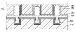
- FIG. 13 is a diagram illustrating an example of the configuration of a pixel according to a seventh embodiment of the present disclosure.
- FIG. 13A to 13C are diagrams illustrating an example of a manufacturing method of a light detection element according to a seventh embodiment of 13A to 13C are diagrams illustrating an example of a manufacturing method of a light detection element according to a seventh embodiment of FIG. 23 is a diagram illustrating an example of the configuration of a pixel according to an eighth embodiment of the present disclosure.
- FIG. 23 is a diagram showing another configuration example of a pixel according to the eighth embodiment of the present disclosure.
- 1 is a block diagram showing an example of the configuration of an imaging device mounted on an electronic device.
- 1 is a block diagram showing a schematic configuration example of a vehicle control system
- 4 is an explanatory diagram showing an example of the installation positions of an outside-vehicle information detection unit and an imaging unit;
- the pixel 100 generates a pixel signal under the control of a control signal transmitted by the signal line 11, and outputs the generated pixel signal via the signal line 12.
- the signal line 11 is arranged for each row in the shape of a two-dimensional matrix, and is wired in common to a plurality of pixels 100 arranged in one row.
- the signal line 12 is arranged for each column in the shape of a two-dimensional matrix, and is wired in common to a plurality of pixels 100 arranged in one column.
- the vertical drive unit 20 generates the control signals for the above-mentioned pixels 100.
- the vertical drive unit 20 in the figure generates control signals for each row of the two-dimensional matrix of the pixel array unit 10 and outputs them sequentially via the signal line 11.
- the column signal processing unit 30 processes pixel signals generated by the pixels 100.
- the column signal processing unit 30 in the figure simultaneously processes pixel signals from multiple pixels 100 arranged in one row of the pixel array unit 10, which are transmitted via signal lines 12. This processing can include, for example, analog-to-digital conversion, which converts analog pixel signals generated by the pixels 100 into digital pixel signals, and correlated double sampling (CDS), which removes offset errors in the pixel signals.
- CDS correlated double sampling
- the control unit 40 controls the vertical drive unit 20 and the column signal processing unit 30.
- the control unit 40 in the figure controls the vertical drive unit 20 and the column signal processing unit 30 by outputting control signals via signal lines 41 and 42, respectively.
- [Configuration of pixel array section] 2 is a diagram showing a configuration example of a pixel array unit according to the first embodiment of the present disclosure.
- the diagram is a plan view showing a configuration example of the pixel array unit 10.
- the pixel array unit 10 is configured by arranging a plurality of pixels 100 in a two-dimensional matrix.
- An on-chip lens 160 is disposed on the light-entering surface of the pixel 100.
- This on-chip lens 160 collects the incident light and transmits incident light of a specified wavelength.
- the letters attached to the on-chip lens 160 indicate the type of incident light that is transmitted. Specifically, "R” indicates red light, "G” indicates green light, and "B” indicates blue light.
- the pixel array section 10 in FIG. 2 shows an example in which on-chip lenses 160 corresponding to incident light of the same color are disposed for two rows and two columns of pixels 100.
- the pixel array section 10 also shows an example in which a group of two rows and two columns of pixels 100 are disposed in a Bayer array.
- a color filter 150 (not shown) is disposed beneath the on-chip lens 160.
- a base material 170 is disposed on the bottom of this color filter 150.
- the dashed circle in FIG. 2 represents the base material 170.
- a light shielding portion 140 is disposed at the boundary between pixels 100. This light shielding portion 140 is disposed between pixels 100 to prevent light from adjacent pixels 100 from mixing. If light from adjacent pixels 100 mixes, crosstalk and color mixing occur, and the image quality of the image data deteriorates. By disposing the light shielding portion 140, crosstalk and the like can be reduced. As described later, the light shielding portion 140 is configured in a wall shape and is configured in a hollow shape. In addition, an opening 144 is disposed in the light shielding portion 140. This opening 144 is used to remove a temporary wall portion 149 (not shown) disposed inside the light shielding portion 140 when making the light shielding portion 140 hollow. A manufacturing method for the light shielding portion 140 will be described later in detail.
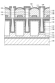
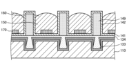
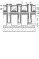
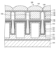
- FIG. 3 is a diagram showing a configuration example of a pixel according to the first embodiment of the present disclosure.
- the figure is a cross-sectional view showing the configuration example of a pixel 100. Note that the figure is a cross-sectional view taken along line AA' in Fig. 2.
- the pixel 100 includes a semiconductor substrate 110, a wiring region 120, a planarization film 134, a light shielding portion 140, a color filter 150, an on-chip lens 160, a base material 170, and an anti-reflection film 171.
- the semiconductor substrate 110 is a semiconductor substrate on which the photoelectric conversion unit 101 of the pixel 100 and the elements of the pixel circuit are formed.
- This semiconductor substrate 110 can be made of silicon (Si).
- the semiconductor substrate 110 in FIG. 3 is assumed to form a p-type well region. An element can be formed by placing an n-type or p-type semiconductor region in this well region. The open rectangles represent the semiconductor regions.
- FIG. 3 shows the n-type semiconductor region 111 that forms the photoelectric conversion unit 101. The pn junction at the interface between the semiconductor region 111 and the surrounding well region forms a photodiode.
- a wiring region 120 is arranged on the front surface of the semiconductor substrate 110 with an insulating film 119 interposed between them.
- This wiring region 120 is an area in which wiring that transmits signals, etc. to the elements of the pixel 100 is arranged.
- a planarization film 134 is disposed on the rear surface of the semiconductor substrate 110. This planarization film 134 planarizes the rear surface of the semiconductor substrate 110.
- the planarization film 134 can be made of, for example, silicon oxide (SiO x ), silicon nitride (SiN), and silicon oxynitride (SiON).
- an isolation portion 133 is disposed in an area of the semiconductor substrate 110 at the boundary between the pixels 100. This isolation portion 133 insulates the pixels 100 from each other.
- the isolation portion 133 can be made of, for example, silicon oxide ( SiOx ), silicon nitride (SiN) and silicon oxynitride (SiON).
- the isolation portion 133 can be formed by disposing SiOx or the like in a groove-shaped recess 130 formed in the semiconductor substrate 110.
- the isolation portion 133 can be made of the same material as the planarization film 134.
- a pinning layer 131 can be disposed on the rear surface of the semiconductor substrate 110 including the wall surface of the recess 130. This pinning layer 131 suppresses the generation of dark current caused by the interface state of the semiconductor substrate 110.
- the pinning layer 131 can be made of a high dielectric material having a negative fixed charge.
- the pinning layer 131 can be made of, for example, hafnium oxide (HfO 2 ), zirconium oxide (ZrO 2 ), aluminum oxide (Al 2 O 3 ), tantalum oxide (Ta 2 O 5 ), titanium oxide (TiO 2 ), magnesium oxide (MgO), yttrium oxide (Y 2 O 3 ), or the like.
- An anti-reflection layer 132 can also be disposed on the rear surface of the semiconductor substrate 110 including the wall surfaces of the recess 130. This anti-reflection layer 132 is disposed adjacent to the pinning layer 131.
- the anti-reflection layer 132 can be made of an insulating material having a refractive index smaller than that of the high dielectric material forming the pinning layer 131.
- the anti-reflection layer 132 can be made of, for example, tantalum oxide (Ta 2 O 5 ).
- the color filter 150 transmits light of a specific wavelength from among the light incident on the pixel 100.
- the color filter 150 is arranged on the pixel 100 in such a way that one of the color filters 150 corresponding to red light, green light, or blue light is arranged on the pixel 100.
- This color filter 150 can be made of a resin containing a pigment or the like that transmits light of a specific wavelength.
- the light shielding portion 140 is disposed at the boundary between the pixels 100 adjacent to the color filter 150 to shield incident light.
- This light shielding portion 140 is configured as a hollow structure.
- the light shielding portion 140 includes a wall portion 142 and a gap 143 formed inside the wall portion 142.
- the planarization film 134 forms part of the wall portion.
- the gap 143 is filled with a gas such as air. Since the refractive index of air is smaller than that of the material that constitutes the color filter 150, the incident light is reflected by the light shielding portion 140. This makes it possible to prevent the incident light from mixing with the adjacent pixels 100.
- An insulating film 141 is disposed on the bottom of the color filter 150.
- This insulating film 141 is made of the same material as the wall portion 142 and is formed at the same time as the wall portion 142.
- the on-chip lens 160 focuses incident light of a specific wavelength and makes it incident on the photoelectric conversion unit 101 through the color filter 150.
- This on-chip lens 160 is made of a material that transmits incident light of a specific wavelength, like the color filter 150. Furthermore, the incident surface of this on-chip lens 160 is formed into a curved surface.
- the on-chip lens 160 can be made of a resin that contains a pigment or the like that transmits light of a specific wavelength.
- the on-chip lens 160 and the color filter 150 that transmit incident light of the same wavelength can be arranged in the pixel 100. Furthermore, the on-chip lens 160 can be arranged adjacent to the color filter 150.
- FIG. 3 shows an example in which the on-chip lens 160 is formed integrally with the color filter 150.
- a base material 170 is disposed adjacent to the insulating film 141 at the bottom of the color filter 150 in FIG. 3.
- the base material 170 is configured to be smaller than the color filter 150 when viewed from the normal direction of the semiconductor substrate 110.
- the base material 170 is used to control the surface shape of the on-chip lens 160. That is, by disposing the base material 170, the surface of the on-chip lens 160 can be made into a convex curved surface.
- the height of the base material 170 is configured to be equal to or lower than the height of the light shielding portion 140.
- the base material 170 can be configured from a member having a refractive index equal to or lower than that of the semiconductor substrate 110, for example, silicon dioxide (SiO 2 ).
- the anti-reflection film 171 is disposed on the surfaces of the on-chip lens 160 and the light shielding portion 140 to prevent reflection of incident light.
- the anti-reflection film 171 can be made of, for example, SiO2 .
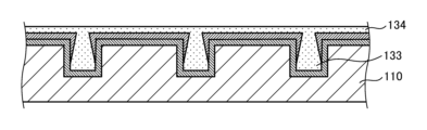
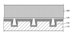
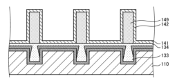
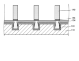
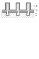
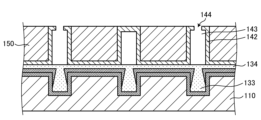
- FIGS. 4A to 4K are diagrams illustrating an example of a manufacturing method of a photodetector according to the first embodiment of the present disclosure.
- Figures 4A to 4K are diagrams illustrating an example of a manufacturing process of a portion of a pixel 100 of a photodetector 1. Note that in Figures 4A to 4K, the wiring region 120 and the like are omitted.
- a semiconductor region of the element is formed in the semiconductor substrate 110.
- a wiring region 120 is arranged on the front surface of the semiconductor substrate 110.
- a recess 130 is formed on the back surface of the semiconductor substrate 110, and a pinning layer 131 and an anti-reflection layer 132 are arranged.
- an isolation portion 133 and a planarization film 134 are arranged (FIG. 4A).
- This material film 400 can be composed of, for example, amorphous silicon or copper-containing aluminum (AlCu).
- a resist 401 is placed on the material film 400.
- An opening 402 is placed in this resist 401 in an area other than the area where the light shielding portion 140 is to be formed (FIG. 4C).
- the material film 400 is etched using the resist 401 as a mask to form a temporary wall portion 149 ( Figure 4D).
- an insulating film is formed on the back side of the semiconductor substrate 110, including the surface of the temporary wall portion 149, to form the insulating film 141 and the wall portion 142 ( Figure 4E).
- the base material 170 is placed on the insulating film 141 between the temporary wall portions 149 ( Figure 4F). This can be done by placing a film of the base material 170 on the back side of the semiconductor substrate 110 and then etching away any unnecessary portions.
- the color filter 150 and the on-chip lens 160 are placed between the temporary wall portions 149 (FIG. 4G).
- the surface of the on-chip lens 160 is curved due to the action of the base material 170.
- an anti-reflection film 171 is disposed on the surfaces of the on-chip lens 160 and the light shielding portion 140 (FIG. 4H).
- the anti-reflection film 171 can be a SiO 2 film formed by ALD (Atomic Layer Deposition).
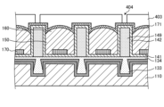
- resist 403 is placed ( Figure 4I).
- openings 404 are placed in the areas where openings 144 are to be formed.
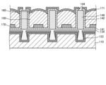
- the anti-reflection film 171 and the wall portion 142 are etched using the resist 403 as a mask to form the opening 144 (FIG. 4J).
- the temporary wall portion 149 is exposed in the opening 144.
- the temporary wall portion 149 is etched through the opening 144. This forms the gap 143, and the light-shielding portion 140 is formed (FIG. 4K). Note that wet etching or dry etching can be used to etch the temporary wall portion 149. Through the above steps, the pixel 100 can be manufactured.
- the configuration of the light detection element 1 is not limited to this example.
- the anti-reflection film 171 of the pixel 100 may be omitted.
- the anti-reflection layer 132 may also be omitted.
- the light-shielding portion 140 including the gap 143 is disposed adjacent to the color filter 150 and on-chip lens 160 of the pixel 100. This makes it possible to reduce crosstalk and color mixing in the pixel 100 having the on-chip lens 160 that collects incident light of a specific wavelength.
- the photodetection element 1 of the first embodiment described above includes the light-shielding portion 140 having the gap 143.
- the photodetection element 1 of the second embodiment of the present disclosure differs from the first embodiment described above in that a light-shielding film is disposed in the light-shielding portion 140.
- the light-shielding film 145 is disposed at the bottom of the gap 143 of the light-shielding portion 140 to block incident light.
- This light-shielding film 145 can be made of a material that absorbs light or a material that reflects light.
- the light-shielding film 145 can be made of a single layer film of titanium (Ti), titanium nitride (TiN), tantalum (Ta), and tantalum nitride (TaN), or a laminate film of these materials. By disposing this light-shielding film 145, the light-shielding ability of the light-shielding portion 140 can be improved.
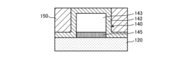
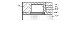
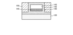
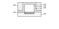
- FIGS. 6A to 6F are diagrams showing configuration examples of a light-shielding film according to a second embodiment of the present disclosure, and are cross-sectional views showing variations of the light-shielding film 145.
- FIG. 6A shows an example of a light-shielding film 145 configured to have approximately the same width as the gap 143.
- FIG. 6B shows an example of a light-shielding film 145 configured to have a width narrower than the gap 143.
- FIG. 6C shows an example of a light-shielding film 145 configured to have a width wider than the gap 143.
- FIG. 6D shows an example of a light-shielding film 145 whose bottom surface is configured at the same height from the surface of the semiconductor substrate 110 as the bottom surface of the color filter 150.
- FIG. 6E shows an example of a light-shielding film 145 whose bottom surface is configured above the bottom surface of the color filter 150.
- FIG. 6F shows an example of a light-shielding film 145 whose bottom surface is configured below the bottom surface of the color filter 150.
- FIGS. 7A and 7B are diagrams illustrating an example of a manufacturing method of a photodetector according to the second embodiment of the present disclosure.
- 7A and 7B are diagrams illustrating an example of a manufacturing process of a portion of a pixel 100 of a photodetector 1.
- FIG. 4A First, the process in FIG. 4A is carried out. Next, a material film 405 for the light-shielding film 145 and a material film 400 for the temporary wall portion 149 are laminated in this order on the back side of the semiconductor substrate 110 (FIG. 7A).
- the material film 405 and the material film 400 are etched to form the light-shielding film 145 and the temporary wall portion 149 (FIG. 7B). Thereafter, the steps of FIGS. 4E-4K are performed to manufacture the pixel 100 having the light-shielding film 145.
- the configuration of the light detection element 1 other than that described above is the same as the configuration of the light detection element 1 in the first embodiment of the present disclosure, so the description will be omitted.
- the light detection element 1 of the second embodiment of the present disclosure can improve the light blocking ability of the light blocking portion 140 by disposing the light blocking film 145 in the light blocking portion 140.
- the photodetection element 1 of the first embodiment described above the on-chip lens 160 and the color filter 150 are disposed in the pixel 100.
- the photodetection element 1 of the third embodiment of the present disclosure differs from the first embodiment described above in that it includes a sealing film that seals the on-chip lens 160 and the color filter 150.
- FIG. 8 is a diagram showing a configuration example of a pixel according to a third embodiment of the present disclosure. Similar to Fig. 3, Fig. 8 is a cross-sectional view showing a configuration example of a pixel 100.
- the pixel 100 in Fig. 8 differs from the pixel 100 in Fig. 3 in that it includes a first sealing film 172 and a second sealing film 173.
- the first sealing film 172 is disposed on the incident surface side of the on-chip lens 160 to seal the on-chip lens 160. This shows an example in which the first sealing film 172 is also disposed on the surface side of the light shielding portion 140. By disposing the first sealing film 172, it is possible to reduce the intrusion of moisture into the on-chip lens 160.
- the second sealing film 173 is disposed inside the wall portion 142 of the light shielding portion 140 to seal the color filter 150. By disposing the second sealing film 173, it is possible to reduce the intrusion of moisture into the color filter 150 via the gap 143.
- the first sealing film 172 and the second sealing film 173 can be made of Al2O3 or SiN.
- the following describes a method for manufacturing a pixel 100 having a first sealing film 172 and a second sealing film 173.
- material films for the first sealing film 172 and the second sealing film 173 are formed on the back surface side of the semiconductor substrate 110.
- the first sealing film 172 is formed on the front surface side of the anti-reflection film 171.
- the second sealing film 173 is formed on the inside of the light-shielding portion 140 through the opening 144.
- the configuration of the light detection element 1 other than that described above is the same as the configuration of the light detection element 1 in the first embodiment of the present disclosure, so the description will be omitted.
- the photodetector element 1 of the third embodiment of the present disclosure has the first sealing film 172 and the second sealing film 173 disposed therein to seal the on-chip lens 160 and the color filter 150. This can reduce deterioration of the on-chip lens 160 and the color filter 150 due to the intrusion of moisture.
- the photodetection element 1 of the above-described third embodiment includes the first sealing film 172 and the second sealing film 173.
- the photodetection element 1 of the fourth embodiment of the present disclosure differs from the above-described third embodiment in that it includes sealing films adjacent to the bottom and side surfaces of the color filter 150.
- FIG. 9 is a diagram showing a configuration example of a pixel according to a fourth embodiment of the present disclosure. Similar to Fig. 8, the figure is a cross-sectional view showing a configuration example of a pixel 100.
- the pixel 100 in the figure differs from the pixel 100 in Fig. 8 in that it includes a third sealing film 174 instead of the first sealing film 172 and the second sealing film 173.
- the third sealing film 174 is disposed near the side and bottom surfaces of the on-chip lens 160 and the color filter 150 to seal the on-chip lens 160 and the color filter 150. By disposing the third sealing film 174, it is possible to reduce the intrusion of moisture into the on-chip lens 160 and the color filter 150.
- the third sealing film 174 can be made of the same material as the first sealing film 172.
- [Method of manufacturing the photodetector] 10 is a diagram showing an example of a manufacturing method of a photodetector according to the fourth embodiment of the present disclosure. The diagram shows an example of a manufacturing process of the pixel 100 portion of the photodetector 1.
- the configuration of the light detection element 1 other than that described above is the same as the configuration of the light detection element 1 in the third embodiment of the present disclosure, so the description will be omitted.
- the third sealing film 174 is disposed to seal the on-chip lens 160 and the color filter 150. This makes it possible to reduce deterioration of the on-chip lens 160 and the color filter 150 due to the intrusion of moisture.
- the photodetection element 1 of the third embodiment includes a first sealing film 172 and a second sealing film 173.
- the photodetection element 1 of the fifth embodiment of the present disclosure differs from the above-described third embodiment in that it further includes a third sealing film 174.
- FIG. 11 is a diagram showing a configuration example of a pixel according to a fifth embodiment of the present disclosure. Similar to Fig. 8, the figure is a cross-sectional view showing a configuration example of a pixel 100. The pixel 100 in the figure differs from the pixel 100 in Fig. 8 in that it further includes a third sealing film 174.
- the configuration of the light detection element 1 other than that described above is the same as the configuration of the light detection element 1 in the third embodiment of the present disclosure, so the description will be omitted.
- the light detection element 1 of the fifth embodiment of the present disclosure includes the first sealing film 172, the second sealing film 173, and the third sealing film 174. This can further reduce the deterioration of the on-chip lens 160 and the color filter 150 due to the intrusion of moisture.
- the opening 144 is formed in the light-shielding portion 140 of the pixel 100.
- the photodetection element 1 of the sixth embodiment of the present disclosure differs from the first embodiment described above in that the opening 144 is blocked.
- FIG. 12 is a diagram showing a configuration example of a pixel array section according to a sixth embodiment of the present disclosure. Similar to Fig. 2, Fig. 12 is a plan view showing a configuration example of the pixel array section 10.
- the dashed circle drawn on the light shielding section 140 in Fig. 12 represents an opening 144.
- the pixel array section 10 in Fig. 12 differs from the pixel array section 10 in Fig. 2 in that the opening 144 is blocked.
- FIG. 13 is a diagram showing a configuration example of a pixel according to a sixth embodiment of the present disclosure. Similar to Fig. 3, Fig. 13 is a cross-sectional view showing a configuration example of a pixel 100. The pixel 100 in Fig. 13 differs from the pixel 100 in Fig. 3 in that it further includes a blocking film 179.
- the blocking film 179 is disposed on the upper surface of the light shielding portion 140 to block the opening 144. By disposing this blocking film 179 to block the opening 144, it is possible to prevent moisture from entering the inside of the light shielding portion 140.
- the blocking film 179 in FIG. 13 is also disposed between the color filter 150 and the on-chip lens 160.
- the blocking film 179 can be made of an insulating material such as silicon oxide (SiOx), silicon nitride (SiN), and silicon oxynitride (SiON).
- the wall portion 142 and the blocking film 179 can be made of different materials. For example, the wall portion 142 can be made of SiOx, and the blocking film 179 can be made of SiN.
- a film of the blocking film 179 material may be formed on the wall portion 142 of the light blocking portion 140 through the opening 144.
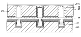
- FIGS. 14A to 14F are diagrams illustrating an example of a manufacturing method of a photodetector according to the sixth embodiment of the present disclosure.
- Figures 14A to 14F are diagrams illustrating an example of a manufacturing process of the pixel 100 portion of the photodetector 1.
- a resist 411 is placed on the back surface side of the semiconductor substrate 110.
- An opening 412 is formed in this resist 411 in the area where the opening 144 is to be formed ( Figure 14B).
- the wall portion 142 is etched using the resist 411 as a mask to form the opening 144.
- the resist 411 is then removed ( Figure 14C).
- a blocking film 179 is placed on the back side of the semiconductor substrate 110 ( Figure 14E).
- an on-chip lens 160 is formed ( Figure 14F).
- the configuration of the light detection element 1 other than that described above is the same as the configuration of the light detection element 1 in the first embodiment of the present disclosure, so the description will be omitted.
- the light detection element 1 of the sixth embodiment of the present disclosure has a blocking film 179 disposed therein to block the opening 144. This can reduce the intrusion of moisture into the light-shielding portion 140.
- the color filter 150 and the on-chip lens 160 are separated by the blocking film 179.
- the photodetection element 1 of the seventh embodiment of the present disclosure differs from the sixth embodiment described above in that the color filter 150 and the on-chip lens 160 are disposed adjacent to each other.
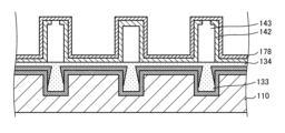
- FIG. 15 is a diagram showing a configuration example of a pixel according to a seventh embodiment of the present disclosure. Similar to Fig. 13, Fig. 15 is a cross-sectional view showing a configuration example of a pixel 100.
- the pixel 100 in Fig. 15 is different from the pixel 100 in Fig. 13 in that it includes an occluding film 178 instead of the occluding film 179, and the color filter 150 and the on-chip lens 160 are disposed adjacent to each other.
- the blocking film 178 is disposed on the upper surface of the light shielding portion 140 to block the opening 144. By disposing this blocking film 178, it is possible to prevent moisture from entering the inside of the light shielding portion 140, similar to the blocking film 179.
- the blocking film 178 is also configured in a shape adjacent to the side and bottom surfaces of the color filter 150. Therefore, in the pixel 100 of FIG. 15, the color filter 150 and the on-chip lens 160 are configured in a shape adjacent to each other.
- the blocking film 178 can be configured from the same material as the blocking film 179.
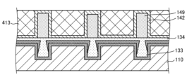
- FIGS. 16A to 16G are diagrams illustrating an example of a manufacturing method of a photodetector according to the seventh embodiment of the present disclosure.
- Figures 16A to 16G are diagrams illustrating an example of a manufacturing process of the pixel 100 portion of the photodetector 1.
- Figures 4A-4E are carried out.
- a filler member 413 is placed between the temporary wall portions 149 ( Figure 16A).
- a resist can be applied to this filler member 413.
- a resist 414 is placed on the back surface side of the semiconductor substrate 110.
- An opening 415 is formed in this resist 414 in the area where the opening 144 is to be formed ( Figure 16B).
- the wall portion 142 is etched using the resist 414 as a mask to form the opening 144.
- the resist 414 is then removed ( Figure 16C).
- a blocking film 178 is placed on the back side of the semiconductor substrate 110 ( Figure 16E).
- a color filter 150 is formed ( Figure 16F).
- the on-chip lens 160 is formed ( Figure 16G). Through the above steps, the pixel 100 can be manufactured.
- the configuration of the light detection element 1 other than that described above is the same as the configuration of the light detection element 1 in the sixth embodiment of the present disclosure, so the description will be omitted.
- the on-chip lens 160 is disposed at the center of the pixel 100.
- the photodetection element 1 of the eighth embodiment of the present disclosure differs from the sixth embodiment described above in that the position of the on-chip lens 160 is adjusted.
- FIG. 17 is a diagram showing a configuration example of a pixel according to an eighth embodiment of the present disclosure. Similar to Fig. 13, Fig. 17 is a cross-sectional view showing a configuration example of a pixel 100. The pixel 100 in Fig. 17 differs from the pixel 100 in Fig. 13 in that the on-chip lens 160 is disposed at a position shifted from the center of the pixel 100.
- the pixel 100 in FIG. 17 shows an example of the pixel 100 arranged in the peripheral portion on the right side of the pixel array section 10 described in FIG.
- the on-chip lens 160 in FIG. 17 can be arranged in a position shifted to the left of FIG. 17 with respect to the center of the pixel 100. In this way, the on-chip lens 160 can adjust its position in the pixel 100 according to the angle of incidence of the incident light.
- Fig. 18 is a diagram showing another configuration example of a pixel according to the eighth embodiment of the present disclosure. Like Fig. 17, this figure is a cross-sectional view showing a configuration example of a pixel 100.
- the pixel 100 in this figure shows an example in which pupil correction is performed in the pixel 100 in which the blocking film 178 described in Fig. 15 is arranged.
- the position of the on-chip lens 160 can also be adjusted according to the incident angle of incident light.
- the configuration of the light detection element 1 other than that described above is the same as the configuration of the light detection element 1 in the sixth embodiment of the present disclosure, so the description will be omitted.
- the photodetector element 1 adjusts the position of the on-chip lens 160 in the pixel 100 according to the angle of incidence of the incident light. This makes it possible to prevent a decrease in the sensitivity of the pixels 100 in the peripheral portion of the pixel array section 10.
- the photodetector element 1 as described above can be applied to various electronic devices, such as imaging systems such as digital still cameras and digital video cameras, mobile phones with imaging functions, and other devices with imaging functions.
- FIG. 19 is a block diagram showing an example of the configuration of an imaging device mounted on an electronic device.
- an electronic device 701 includes an optical system 702, a photodetector 703, and a DSP (Digital Signal Processor) 704, and is configured by connecting the DSP 704, a display device 705, an operation system 706, a memory 708, a recording device 709, and a power supply system 710 via a bus 707, and is capable of capturing still and moving images.
- DSP Digital Signal Processor
- the optical system 702 is composed of one or more lenses, and guides image light (incident light) from the subject to the light detection device 703, forming an image on the light receiving surface (sensor section) of the light detection device 703.
- the photodetector 703 is implemented with the photodetector element 1 of any of the configuration examples described above. Electrons are accumulated in the photodetector 703 for a certain period of time in accordance with an image formed on the light receiving surface via the optical system 702. A signal corresponding to the electrons accumulated in the photodetector 703 is then input to the DSP 704.
- the DSP 704 performs various signal processing on the signal from the light detection device 703 to obtain an image, and temporarily stores the image data in the memory 708.
- the image data stored in the memory 708 is recorded in the recording device 709 or supplied to the display device 705 to display the image.
- the operation system 706 also accepts various operations by the user and supplies operation signals to each block of the electronic device 701, and the power supply system 710 supplies the power required to drive each block of the electronic device 701.
- FIG. 20 is a block diagram showing a schematic configuration example of a vehicle control system, which is an example of a mobile object control system to which the technology disclosed herein can be applied.
- the vehicle control system 12000 includes a plurality of electronic control units connected via a communication network 12001.
- the vehicle control system 12000 includes a drive system control unit 12010, a body system control unit 12020, an outside vehicle information detection unit 12030, an inside vehicle information detection unit 12040, and an integrated control unit 12050.
- Also shown as functional components of the integrated control unit 12050 are a microcomputer 12051, an audio/video output unit 12052, and an in-vehicle network I/F (Interface) 12053.
- the drive system control unit 12010 controls the operation of devices related to the drive system of the vehicle according to various programs.
- the drive system control unit 12010 functions as a control device for a drive force generating device for generating the drive force of the vehicle, such as an internal combustion engine or a drive motor, a drive force transmission mechanism for transmitting the drive force to the wheels, a steering mechanism for adjusting the steering angle of the vehicle, and a braking device for generating a braking force for the vehicle.
- the body system control unit 12020 controls the operation of various devices installed in the vehicle body according to various programs.
- the body system control unit 12020 functions as a control device for a keyless entry system, a smart key system, a power window device, or various lamps such as headlamps, tail lamps, brake lamps, turn signals, and fog lamps.
- radio waves or signals from various switches transmitted from a portable device that replaces a key can be input to the body system control unit 12020.
- the body system control unit 12020 accepts the input of these radio waves or signals and controls the vehicle's door lock device, power window device, lamps, etc.
- the outside-vehicle information detection unit 12030 detects information outside the vehicle equipped with the vehicle control system 12000.
- the image capturing unit 12031 is connected to the outside-vehicle information detection unit 12030.
- the outside-vehicle information detection unit 12030 causes the image capturing unit 12031 to capture images outside the vehicle and receives the captured images.
- the outside-vehicle information detection unit 12030 may perform object detection processing or distance detection processing for people, cars, obstacles, signs, characters on the road surface, etc. based on the received images.
- the imaging unit 12031 is an optical sensor that receives light and outputs an electrical signal according to the amount of light received.
- the imaging unit 12031 can output the electrical signal as an image, or as distance measurement information.
- the light received by the imaging unit 12031 may be visible light, or may be invisible light such as infrared light.
- the in-vehicle information detection unit 12040 detects information inside the vehicle.
- a driver state detection unit 12041 that detects the state of the driver is connected.
- the driver state detection unit 12041 includes, for example, a camera that captures an image of the driver, and the in-vehicle information detection unit 12040 may calculate the driver's degree of fatigue or concentration based on the detection information input from the driver state detection unit 12041, or may determine whether the driver is dozing off.
- the microcomputer 12051 can calculate the control target values of the driving force generating device, steering mechanism, or braking device based on the information inside and outside the vehicle acquired by the outside vehicle information detection unit 12030 or the inside vehicle information detection unit 12040, and output a control command to the drive system control unit 12010.
- the microcomputer 12051 can perform cooperative control aimed at realizing the functions of an ADAS (Advanced Driver Assistance System), including avoiding or mitigating vehicle collisions, following based on the distance between vehicles, maintaining vehicle speed, vehicle collision warning, or vehicle lane departure warning.
- ADAS Advanced Driver Assistance System
- the microcomputer 12051 can also perform cooperative control for the purpose of autonomous driving, which allows the vehicle to travel autonomously without relying on the driver's operation, by controlling the driving force generating device, steering mechanism, braking device, etc. based on information about the surroundings of the vehicle acquired by the outside vehicle information detection unit 12030 or the inside vehicle information detection unit 12040.
- the microcomputer 12051 can also output control commands to the body system control unit 12020 based on information outside the vehicle acquired by the outside information detection unit 12030. For example, the microcomputer 12051 can control the headlamps according to the position of a preceding vehicle or an oncoming vehicle detected by the outside information detection unit 12030, and perform cooperative control aimed at preventing glare, such as switching from high beams to low beams.
- FIG. 21 shows an example of the installation position of the imaging unit 12031.
- the imaging unit 12031 includes imaging units 12101, 12102, 12103, 12104, and 12105.
- the imaging units 12101, 12102, 12103, 12104, and 12105 are provided, for example, at the front nose, side mirrors, rear bumper, back door, and upper part of the windshield inside the vehicle cabin of the vehicle 12100.
- the imaging unit 12101 provided at the front nose and the imaging unit 12105 provided at the upper part of the windshield inside the vehicle cabin mainly acquire images of the front of the vehicle 12100.
- the imaging units 12102 and 12103 provided at the side mirrors mainly acquire images of the sides of the vehicle 12100.
- the imaging unit 12104 provided at the rear bumper or back door mainly acquires images of the rear of the vehicle 12100.
- the imaging unit 12105 provided at the upper part of the windshield inside the vehicle cabin is mainly used to detect leading vehicles, pedestrians, obstacles, traffic lights, traffic signs, lanes, etc.
- FIG. 21 shows an example of the imaging ranges of the imaging units 12101 to 12104.
- Imaging range 12111 indicates the imaging range of the imaging unit 12101 provided on the front nose
- imaging ranges 12112 and 12113 indicate the imaging ranges of the imaging units 12102 and 12103 provided on the side mirrors, respectively
- imaging range 12114 indicates the imaging range of the imaging unit 12104 provided on the rear bumper or back door.
- an overhead image of the vehicle 12100 viewed from above is obtained by superimposing the image data captured by the imaging units 12101 to 12104.
- At least one of the imaging units 12101 to 12104 may have a function of acquiring distance information.
- at least one of the imaging units 12101 to 12104 may be a stereo camera consisting of multiple imaging elements, or an imaging element having pixels for phase difference detection.
- the microcomputer 12051 can obtain the distance to each solid object within the imaging ranges 12111 to 12114 and the change in this distance over time (relative speed with respect to the vehicle 12100) based on the distance information obtained from the imaging units 12101 to 12104, and can extract as a preceding vehicle, in particular, the closest solid object on the path of the vehicle 12100 that is traveling in approximately the same direction as the vehicle 12100 at a predetermined speed (e.g., 0 km/h or faster). Furthermore, the microcomputer 12051 can set the inter-vehicle distance that should be maintained in advance in front of the preceding vehicle, and perform automatic braking control (including follow-up stop control) and automatic acceleration control (including follow-up start control). In this way, cooperative control can be performed for the purpose of automatic driving, which runs autonomously without relying on the driver's operation.
- automatic braking control including follow-up stop control
- automatic acceleration control including follow-up start control
- the microcomputer 12051 classifies and extracts three-dimensional object data on three-dimensional objects, such as two-wheeled vehicles, ordinary vehicles, large vehicles, pedestrians, utility poles, and other three-dimensional objects, based on the distance information obtained from the imaging units 12101 to 12104, and can use the data to automatically avoid obstacles.
- the microcomputer 12051 distinguishes obstacles around the vehicle 12100 into obstacles that are visible to the driver of the vehicle 12100 and obstacles that are difficult to see.
- the microcomputer 12051 determines the collision risk, which indicates the risk of collision with each obstacle, and when the collision risk is equal to or exceeds a set value and there is a possibility of a collision, it can provide driving assistance for collision avoidance by outputting an alarm to the driver via the audio speaker 12061 or the display unit 12062, or by performing forced deceleration or avoidance steering via the drive system control unit 12010.
- At least one of the imaging units 12101 to 12104 may be an infrared camera that detects infrared rays.
- the microcomputer 12051 can recognize a pedestrian by determining whether or not a pedestrian is present in the image captured by the imaging units 12101 to 12104. The recognition of such a pedestrian is performed, for example, by a procedure of extracting feature points in the image captured by the imaging units 12101 to 12104 as infrared cameras, and a procedure of performing pattern matching processing on a series of feature points that indicate the contour of an object to determine whether or not it is a pedestrian.
- the audio/image output unit 12052 controls the display unit 12062 to superimpose a rectangular contour line for emphasis on the recognized pedestrian.
- the audio/image output unit 12052 may also control the display unit 12062 to display an icon or the like indicating a pedestrian at a desired position.
- the technology of the present disclosure can be applied to the imaging unit 12031.
- the light detection element 1 of FIG. 1 can be applied to the imaging unit 12031.
- the configuration of the third embodiment of the present disclosure can be applied to the other embodiments.
- the first sealing film 172 and the second sealing film 173 in FIG. 11 can be applied to the second and sixth to eighth embodiments of the present disclosure.
- the configuration of the fourth embodiment of the present disclosure can be applied to other embodiments.
- the third sealing film 174 of FIG. 9 can be applied to the second and sixth to eighth embodiments of the present disclosure.
- the present technology can also be configured as follows. (1) a pixel including a photoelectric conversion unit disposed on a semiconductor substrate and performing photoelectric conversion of incident light, and a color filter that transmits incident light of a predetermined wavelength out of the incident light and allows the incident light to be incident on the photoelectric conversion unit; an on-chip lens disposed at the pixel, made of a member that transmits incident light of a predetermined wavelength among the incident light, having an incident surface for the incident light formed into a curved surface, and condensing the incident light of the predetermined wavelength to cause the incident light to be incident on the photoelectric conversion unit via the color filter; a light-shielding portion disposed on a boundary of the pixel adjacent to the color filter and including a wall portion and a gap formed inside the wall portion.
- the light detection element according to any one of (1) to (11), further comprising a light-shielding film disposed on a bottom of the gap of the light-shielding portion.
Landscapes
- Solid State Image Pick-Up Elements (AREA)
- Spectrometry And Color Measurement (AREA)
- Transforming Light Signals Into Electric Signals (AREA)
Abstract
空隙を使用する遮光部を画素に配置する。光検出素子は、画素と、オンチップレンズと、遮光部とを有する。画素は、半導体基板に配置されて入射光の光電変換を行う光電変換部及び入射光のうちの所定の波長の入射光を透過させて光電変換部に入射させるカラーフィルタを備える。オンチップレンズは、画素に配置されて、入射光のうちの所定の波長の入射光を透過する部材により構成されるとともに入射光の入射面が曲面に形成され、所定の波長の入射光を集光してカラーフィルタを介して光電変換部に入射させる。遮光部は、カラーフィルタに隣接する画素の境界に配置されて壁部及び当該壁部の内側に形成される空隙を備える。
Description
本開示は、光検出素子に関する。
被写体を撮像する光検出素子(撮像素子)は、複数の画素が2次元行列状に配置されて構成される。この画素には、半導体基板に形成されて入射光の光電変換を行う光電変換部、入射光のうちの所定の波長の入射光を透過するカラーフィルタ及び入射光を光電変換部に集光するオンチップレンズ等が配置される。
このような撮像素子において、カラーフィルタをレンズ形状に構成した撮像素子(固体撮像素子)が提案されている(例えば、特許文献1参照)。この固体撮像素子は、カラーフィルタにより入射光の集光を行うため、オンチップレンズが不要となる。これにより、画素における半導体基板上の光学部材を低背化することができ、集光後の入射光の拡散を軽減することができる。また、隣接する画素同士の間には画素間遮光部が配置される。この画素間遮光部は、カラーフィルタより屈折率が低い部材により構成され、隣接する画素からの光の混入を防止する。この画素間遮光部には、例えば、空気を用いることができる。
しかしながら、上記の従来技術では、空気により構成された画素間遮光部が開示されておらず、空気を使用する画素間遮光部を実現できないという問題がある。
そこで、本開示では、レンズ形状に構成されるカラーフィルタを使用する画素を備える光検出素子において、空気等による空隙を低屈折率部として使用する遮光部を画素間に配置する光検出素子を提案する。
本開示に係る光検出素子は、半導体基板に配置されて入射光の光電変換を行う光電変換部及び上記入射光のうちの所定の波長の入射光を透過させて上記光電変換部に入射させるカラーフィルタを備える画素と、上記画素に配置されて、上記入射光のうちの所定の波長の入射光を透過する部材により構成されるとともに上記入射光の入射面が曲面に形成され、上記所定の波長の入射光を集光して上記カラーフィルタを介して上記光電変換部に入射させるオンチップレンズと、上記カラーフィルタに隣接する上記画素の境界に配置されて壁部及び当該壁部の内側に形成される空隙を備える遮光部とを有する。
以下に、本開示の実施形態について図面に基づいて詳細に説明する。説明は、以下の順に行う。なお、以下の各実施形態において、同一の部位には同一の符号を付することにより重複する説明を省略する。
1.第1の実施形態
2.第2の実施形態
3.第3の実施形態
4.第4の実施形態
5.第5の実施形態
6.第6の実施形態
7.第7の実施形態
8.第8の実施形態
9.電子機器の構成
10.移動体への応用例
1.第1の実施形態
2.第2の実施形態
3.第3の実施形態
4.第4の実施形態
5.第5の実施形態
6.第6の実施形態
7.第7の実施形態
8.第8の実施形態
9.電子機器の構成
10.移動体への応用例
(1.第1の実施形態)
[光検出装置の構成]
図1は、本開示の実施形態に係る光検出素子の構成例を示す図である。同図は、光検出素子1の構成例を表すブロック図である。光検出素子1は、被写体の画像データを構成する画素信号を生成して出力する半導体素子である。光検出素子1は、画素アレイ部10と、垂直駆動部20と、カラム信号処理部30と、制御部40とを備える。
[光検出装置の構成]
図1は、本開示の実施形態に係る光検出素子の構成例を示す図である。同図は、光検出素子1の構成例を表すブロック図である。光検出素子1は、被写体の画像データを構成する画素信号を生成して出力する半導体素子である。光検出素子1は、画素アレイ部10と、垂直駆動部20と、カラム信号処理部30と、制御部40とを備える。
画素アレイ部10は、複数の画素100が配置されて構成されたものである。同図の画素アレイ部10は、複数の画素100が2次元行列の形状に配列される例を表したものである。ここで、画素100は、入射光の光電変換を行う光電変換部を備え、照射された入射光に基づいて被写体の画素信号を生成するものである。この光電変換部には、例えば、フォトダイオードを使用することができる。また、画素100には、上述の光電変換部により生成された電荷に基づいて画素信号を生成する画素回路が配置される。それぞれの画素100には、信号線11及び12が配線される。画素100は、信号線11により伝達される制御信号に制御されて画素信号を生成し、信号線12を介して生成した画素信号を出力する。なお、信号線11は、2次元行列の形状の行毎に配置され、1行に配置された複数の画素100に共通に配線される。信号線12は、2次元行列の形状の列毎に配置され、1列に配置された複数の画素100に共通に配線される。
垂直駆動部20は、上述の画素100の制御信号を生成するものである。同図の垂直駆動部20は、画素アレイ部10の2次元行列の行毎に制御信号を生成し、信号線11を介して順次出力する。
カラム信号処理部30は、画素100により生成された画素信号の処理を行うものである。同図のカラム信号処理部30は、信号線12を介して伝達される画素アレイ部10の1行に配置された複数の画素100からの画素信号の処理を同時に行う。この処理として、例えば、画素100により生成されたアナログの画素信号をデジタルの画素信号に変換するアナログデジタル変換や画素信号のオフセット誤差を除去する相関二重サンプリング(CDS:Correlated Double Sampling)を行うことができる。処理後の画素信号は、光検出素子1の外部の回路等に対して出力される。
制御部40は、垂直駆動部20及びカラム信号処理部30を制御するものである。同図の制御部40は、信号線41及び42を介して制御信号をそれぞれ出力して垂直駆動部20及びカラム信号処理部30を制御する。
[画素アレイ部の構成]
図2は、本開示の第1の実施形態に係る画素アレイ部の構成例を示す図である。同図は、画素アレイ部10の構成例を表す平面図である。前述のように、画素アレイ部10は、複数の画素100が2次元行列状に配置されて構成される。
図2は、本開示の第1の実施形態に係る画素アレイ部の構成例を示す図である。同図は、画素アレイ部10の構成例を表す平面図である。前述のように、画素アレイ部10は、複数の画素100が2次元行列状に配置されて構成される。
画素100の入射光の入射面側には、オンチップレンズ160が配置される。この、オンチップレンズ160は、入射光を集光するとともに所定の波長の入射光を透過する。オンチップレンズ160に付された文字は、透過する入射光の種類を表したものである。具体的には、「R」は赤色光を表し、「G」は緑色光を表し、「B」は青色光を表す。図2の画素アレイ部10は、2行2列の画素100に同色の入射光に対応するオンチップレンズ160がそれぞれ配置される例を表したものである。また、画素アレイ部10は、この2行2列の画素100群がベイヤー配列に配置される例を表したものである。
オンチップレンズ160の下層には、カラーフィルタ150(不図示)が配置される。このカラーフィルタ150の底部に下地材170が配置される。図2の破線の円は下地材170を表す。この下地材170を配置することにより、オンチップレンズ160の表面を曲面に構成することができる。
画素100の境界には遮光部140が配置される。この遮光部140は、画素100同士の間に配置され、隣接する画素100からの光の混入を防ぐものである。隣接する画素100からの光が混入する場合、クロストークや混色を生じ、画像データの画質が低下する。遮光部140を配置することにより、クロストーク等を軽減することができる。後述するように、遮光部140は、壁状に構成されるとともに中空形状に構成される。また、遮光部140には、開口部144が配置される。この開口部144は、遮光部140を中空形状にする際に遮光部140の内部に配置された仮壁部149(不図示)を除去するために使用される。遮光部140の製造方法の詳細については後述する。
[画素の構成]
図3は、本開示の第1の実施形態に係る画素の構成例を示す図である。同図は、画素100の構成例を表す断面図である。なお、同図は、図2のA-A’線に沿った断面図である。画素100は、半導体基板110と、配線領域120と、平坦化膜134と、遮光部140と、カラーフィルタ150と、オンチップレンズ160と、下地材170と、反射防止膜171とを備える。
図3は、本開示の第1の実施形態に係る画素の構成例を示す図である。同図は、画素100の構成例を表す断面図である。なお、同図は、図2のA-A’線に沿った断面図である。画素100は、半導体基板110と、配線領域120と、平坦化膜134と、遮光部140と、カラーフィルタ150と、オンチップレンズ160と、下地材170と、反射防止膜171とを備える。
半導体基板110は、画素100の光電変換部101や画素回路の素子が形成される半導体の基板である。この半導体基板110は、シリコン(Si)により構成することができる。図3の半導体基板110は、便宜上、p型のウェル領域を構成するものと想定する。このウェル領域にn型又はp型の半導体領域を配置することにより、素子を形成することができる。白抜きの矩形が半導体領域を表す。図3には、光電変換部101を構成するn型の半導体領域111を記載した。半導体領域111と周囲のウェル領域との界面のpn接合がフォトダイオードを構成する。
半導体基板110の表側の表面には絶縁膜119を介して配線領域120が配置される。この配線領域120は、画素100の素子に信号等を伝達する配線が配置される領域である。
半導体基板110の裏側の表面には、平坦化膜134が配置される。この平坦化膜134は、半導体基板110の裏側の表面を平坦化するものである。平坦化膜134は、例えば、酸化シリコン(SiOX)、窒化シリコン(SiN)及び酸窒化シリコン(SiON)により構成することができる。
また、画素100の境界の半導体基板110の領域には、分離部133が配置される。この分離部133は、画素100同士を絶縁するものである。分離部133は、例えば、酸化シリコン(SiOX)、窒化シリコン(SiN)及び酸窒化シリコン(SiON)により構成することができる。分離部133は、半導体基板110に形成された溝状の凹部130にSiOX等を配置することにより形成することができる。なお、分離部133は、平坦化膜134と同じ材料により構成することができる。
凹部130の壁面を含む半導体基板110の裏側の表面には、ピニング層131を配置することができる。このピニング層131は、半導体基板110の界面準位に起因する暗電流の発生を抑制するものである。ピニング層131は、負の固定電荷を有する高誘電体材料により構成することができる。ピニング層131は、例えば、酸化ハフニウム(HfO2)、酸化ジルコニウム(ZrO2)、酸化アルミニウム(Al2O3)、酸化タンタル(Ta2O5)、酸化チタン(TiO2)、酸化マグネシウム(MgO)及び酸化イットリウム(Y2O3)等により構成することができる。
また、凹部130の壁面を含む半導体基板110の裏側の表面には、反射防止層132を配置することもできる。この反射防止層132は、ピニング層131に隣接して配置される。反射防止層132は、ピニング層131を形成する高誘電体材料の屈折率よりも屈折率が小さい絶縁性材料により構成することができる。反射防止層132は、例えば、酸化タンタル(Ta2O5)により構成することができる。
カラーフィルタ150は、画素100の入射光のうちの所定の波長の入射光を透過するものである。前述したオンチップレンズ160と同様に、カラーフィルタ150は、赤色光、緑色光及び青色光に対応するカラーフィルタ150の何れかが画素100に配置される。このカラーフィルタ150は、所定の波長の光を透過する顔料等を含む樹脂により構成することができる。
遮光部140は、カラーフィルタ150に隣接する画素100の境界に配置されて入射光を遮光するものである。この遮光部140は、中空構造に構成される。具体的には、遮光部140は、壁部142及び当該壁部142の内側に形成される空隙143を備える。図3の遮光部140は、平坦化膜134が壁部の一部を構成する。空隙143には、空気等のガスが充填される。空気は、屈折率がカラーフィルタ150を構成する部材より小さいため、入射光は遮光部140により反射される。これにより、隣接する画素100への入射光の混入を防ぐことができる。
カラーフィルタ150の底部には絶縁膜141が配置される。この絶縁膜141は、壁部142と同じ部材により構成され、壁部142と同時に形成される。
オンチップレンズ160は、所定の波長の入射光を集光してカラーフィルタ150を介して光電変換部101に入射させるものである。このオンチップレンズ160は、カラーフィルタ150と同様に入射光のうちの所定の波長の入射光を透過する部材により構成される。更に、このオンチップレンズ160は、入射光の入射面が曲面に形成される。オンチップレンズ160は、所定の波長の光を透過する顔料等を含む樹脂により構成することができる。画素100には、同じ波長の入射光を透過するオンチップレンズ160及びカラーフィルタ150を配置することができる。また、オンチップレンズ160は、カラーフィルタ150に隣接して配置することができる。
また、図3のオンチップレンズ160は、カラーフィルタ150と一体に形成される例を表したものである。図3のカラーフィルタ150の底部の絶縁膜141に隣接して下地材170が配置される。この下地材170は、半導体基板110の法線方向から見てカラーフィルタ150のサイズより小さいサイズに構成される。下地材170は、オンチップレンズ160の表面形状を制御するために使用される。すなわち、下地材170を配置することにより、オンチップレンズ160の表面を凸形状の曲面にすることができる。下地材170の高さは、遮光部140の高さ以下に構成される。また、下地材170は、半導体基板110と同等以下の屈折率の部材、例えば、二酸化ケイ素(SiO2)により構成することができる。
反射防止膜171は、オンチップレンズ160及び遮光部140の表面に配置されて入射光の反射を防止するものである。この反射防止膜171は、例えば、SiO2により構成することができる。
[光検出素子の製造方法]
図4A-4Kは、本開示の第1の実施形態に係る光検出素子の製造方法の一例を示す図である。図4A-4Kは、光検出素子1のうちの画素100の部分の製造工程の一例を表す図である。なお、図4A-4Kにおいては、配線領域120等の記載を省略している。
図4A-4Kは、本開示の第1の実施形態に係る光検出素子の製造方法の一例を示す図である。図4A-4Kは、光検出素子1のうちの画素100の部分の製造工程の一例を表す図である。なお、図4A-4Kにおいては、配線領域120等の記載を省略している。
まず、半導体基板110に素子の半導体領域を形成する。次に、半導体基板110の表側の表面に配線領域120を配置する。次に、半導体基板110の裏側の表面から凹部130を形成し、ピニング層131及び反射防止層132を配置する。次に、分離部133及び平坦化膜134を配置する(図4A)。
次に、半導体基板110の裏面側に仮壁部149の材料膜400を配置する。この材料膜400は、例えば、非晶質シリコンや銅含有アルミニウム(AlCu)により構成することができる。
次に、材料膜400の上にレジスト401を配置する。このレジスト401には、遮光部140を形成する領域以外の領域に開口部402が配置される(図4C)。
次に、レジスト401をマスクとして使用して材料膜400のエッチングを行い、仮壁部149を形成する(図4D)。
次に、仮壁部149の表面を含む、半導体基板110の裏面側に絶縁物の膜を成膜し、絶縁膜141及び壁部142を形成する(図4E)。
次に、仮壁部149の間の絶縁膜141の上に、下地材170を配置する(図4F)。これは、半導体基板110の裏面側に下地材170の材料膜を配置し、不要な部分をエッチングして除去することにより行うことができる。
次に、仮壁部149の間に、カラーフィルタ150及びオンチップレンズ160を配置する(図4G)。下地材170の作用により、オンチップレンズ160の表面が曲面形状となる。
次に、オンチップレンズ160及び遮光部140の表面に反射防止膜171を配置する(図4H)。反射防止膜171には、ALD(Atomic Layer Deposition)により成膜したSiO2膜を適用することができる。
次に、レジスト403を配置する(図4I)。このレジスト403には、開口部144を形成する領域に開口部404が配置される。
次に、レジスト403をマスクとして使用して反射防止膜171及び壁部142のエッチングを行い、開口部144を形成する(図4J)。開口部144にて仮壁部149が露出することとなる。
次に、開口部144を介して仮壁部149のエッチングを行う。これにより、空隙143が形成され、遮光部140が形成される(図4K)。なお、仮壁部149のエッチングには、ウェットエッチング又はドライエッチングを適用することができる。以上の工程により、画素100を製造することができる。
なお、光検出素子1の構成は、この例に限定されない。例えば、画素100の反射防止膜171を省略することもできる。また、反射防止層132を省略することもできる。
このように、本開示の第1の実施形態の光検出素子1は、空隙143を含む遮光部140が画素100のカラーフィルタ150及びオンチップレンズ160に隣接して配置される。これにより、所定の波長の入射光を集光するオンチップレンズ160を有する画素100におけるクロストークや混色を低減することができる。
(2.第2の実施形態)
上述の第1の実施形態の光検出素子1は、空隙143を有する遮光部140を備えていた。これに対し、本開示の第2の実施形態の光検出素子1は、遮光部140に遮光膜を配置する点で、上述の第1の実施形態と異なる。
上述の第1の実施形態の光検出素子1は、空隙143を有する遮光部140を備えていた。これに対し、本開示の第2の実施形態の光検出素子1は、遮光部140に遮光膜を配置する点で、上述の第1の実施形態と異なる。
[画素の構成]
図5は、本開示の第2の実施形態に係る画素の構成例を示す図である。同図は、図3と同様に、画素100の構成例を表す断面図である。同図の画素100は、遮光膜145を更に備える点で、図3の画素100と異なる。
図5は、本開示の第2の実施形態に係る画素の構成例を示す図である。同図は、図3と同様に、画素100の構成例を表す断面図である。同図の画素100は、遮光膜145を更に備える点で、図3の画素100と異なる。
遮光膜145は、遮光部140の空隙143の底部に配置されて入射光を遮光するものである。この遮光膜145は、光を吸収する部材又は光を反射する部材により構成することができる。例えば、遮光膜145は、チタン(Ti)、窒化チタン(TiN)、タンタル(Ta)及び窒化タンタル(TaN)の単層膜やこれらの材料の積層膜により構成することができる。この遮光膜145を配置することにより、遮光部140における遮光能力を向上させることができる。
[遮光膜の構成]
図6A-6Fは、本開示の第2の実施形態に係る遮光膜の構成例を示す図である。図6A-6Fは、遮光膜145のバリエーションを表す断面図である。
図6A-6Fは、本開示の第2の実施形態に係る遮光膜の構成例を示す図である。図6A-6Fは、遮光膜145のバリエーションを表す断面図である。
図6Aは、空隙143と略同じ幅に構成される遮光膜145の例を表したものである。図6Bは、空隙143より狭い幅に構成される遮光膜145の例を表したものである。図6Cは、空隙143よりも広い幅に構成される遮光膜145の例を表したものである。
図6Dは、底面がカラーフィルタ150の底面と同じ半導体基板110の表面からの高さに構成される遮光膜145の例を表したものである。図6Eは、底面がカラーフィルタ150の底面より上側に構成される遮光膜145の例を表したものである。図6Fは、底面がカラーフィルタ150の底面より下側に構成される遮光膜145の例を表したものである。
[光検出素子の製造方法]
図7A及び7Bは、本開示の第2の実施形態に係る光検出素子の製造方法の一例を示す図である。図7A及び7Bは、光検出素子1のうちの画素100の部分の製造工程の一例を表す図である。
図7A及び7Bは、本開示の第2の実施形態に係る光検出素子の製造方法の一例を示す図である。図7A及び7Bは、光検出素子1のうちの画素100の部分の製造工程の一例を表す図である。
まず、図4Aの工程を実行する。次に、半導体基板110の裏面側に遮光膜145の材料膜405及び仮壁部149の材料膜400を順に積層する(図7A)。
次に、材料膜405及び材料膜400のエッチングを行って、遮光膜145及び仮壁部149を形成する(図7B)。その後、図4E-4Kの工程を実行することにより、遮光膜145を有する画素100を製造することができる。
上述した以外の光検出素子1の構成は本開示の第1の実施形態における光検出素子1の構成と同様であるため、説明を省略する。
このように、本開示の第2の実施形態の光検出素子1は、遮光部140に遮光膜145を配置することにより、遮光部140の遮光能力を向上させることができる。
(3.第3の実施形態)
上述の第1の実施形態の光検出素子1は、画素100にオンチップレンズ160及びカラーフィルタ150が配置されていた。これに対し、本開示の第3の実施形態の光検出素子1は、オンチップレンズ160及びカラーフィルタ150を封止する封止膜を備える点で、上述の第1の実施形態と異なる。
上述の第1の実施形態の光検出素子1は、画素100にオンチップレンズ160及びカラーフィルタ150が配置されていた。これに対し、本開示の第3の実施形態の光検出素子1は、オンチップレンズ160及びカラーフィルタ150を封止する封止膜を備える点で、上述の第1の実施形態と異なる。
[画素の構成]
図8は、本開示の第3の実施形態に係る画素の構成例を示す図である。同図は、図3と同様に、画素100の構成例を表す断面図である。同図の画素100は、第1の封止膜172及び第2の封止膜173を備える点で、図3の画素100と異なる。
図8は、本開示の第3の実施形態に係る画素の構成例を示す図である。同図は、図3と同様に、画素100の構成例を表す断面図である。同図の画素100は、第1の封止膜172及び第2の封止膜173を備える点で、図3の画素100と異なる。
第1の封止膜172は、オンチップレンズ160の入射面側に配置されてオンチップレンズ160を封止するものである。また、第1の封止膜172は、遮光部140の表面側にも配置される例を表したものである。第1の封止膜172を配置することにより、オンチップレンズ160への水分の侵入を軽減することができる。
また、第2の封止膜173は、遮光部140の壁部142の内側に配置されてカラーフィルタ150を封止するものである。第2の封止膜173を配置することにより、空隙143を介したカラーフィルタ150への水分の侵入を軽減することができる。第1の封止膜172及び第2の封止膜173は、Al2O3やSiNにより構成することができる。
第1の封止膜172及び第2の封止膜173を有する画素100の製造方法について説明する。まず、図4A-4Kの工程を実行する。次に、第1の封止膜172及び第2の封止膜173の材料膜を半導体基板110の裏面側に成膜する。これにより、反射防止膜171の表面側に第1の封止膜172が形成される。同時に、開口部144を介して遮光部140の内側に第2の封止膜173が形成される。
上述した以外の光検出素子1の構成は本開示の第1の実施形態における光検出素子1の構成と同様であるため、説明を省略する。
このように、本開示の第3の実施形態の光検出素子1は、第1の封止膜172及び第2の封止膜173を配置してオンチップレンズ160及びカラーフィルタ150を封止する。これにより、水分の侵入によるオンチップレンズ160及びカラーフィルタ150の劣化を軽減する構成することができる。
(4.第4の実施形態)
上述の第3の実施形態の光検出素子1は、第1の封止膜172及び第2の封止膜173を備えていた。これに対し、本開示の第4の実施形態の光検出素子1は、カラーフィルタ150の底面及び側面に隣接する封止膜を備える点で、上述の第3の実施形態と異なる。
上述の第3の実施形態の光検出素子1は、第1の封止膜172及び第2の封止膜173を備えていた。これに対し、本開示の第4の実施形態の光検出素子1は、カラーフィルタ150の底面及び側面に隣接する封止膜を備える点で、上述の第3の実施形態と異なる。
[画素の構成]
図9は、本開示の第4の実施形態に係る画素の構成例を示す図である。同図は、図8と同様に、画素100の構成例を表す断面図である。同図の画素100は、第1の封止膜172及び第2の封止膜173の代わりに第3の封止膜174を備える点で、図8の画素100と異なる。
図9は、本開示の第4の実施形態に係る画素の構成例を示す図である。同図は、図8と同様に、画素100の構成例を表す断面図である。同図の画素100は、第1の封止膜172及び第2の封止膜173の代わりに第3の封止膜174を備える点で、図8の画素100と異なる。
第3の封止膜174は、オンチップレンズ160及びカラーフィルタ150の側面及び底面の近傍に配置されてオンチップレンズ160及びカラーフィルタ150を封止するものである。第3の封止膜174を配置することにより、オンチップレンズ160及びカラーフィルタ150への水分の侵入を軽減することができる。第3の封止膜174は、第1の封止膜172と同様の材料により構成することができる。
[光検出素子の製造方法]
図10は、本開示の第4の実施形態に係る光検出素子の製造方法の一例を示す図である。同図は、光検出素子1のうちの画素100の部分の製造工程の一例を表す図である。
図10は、本開示の第4の実施形態に係る光検出素子の製造方法の一例を示す図である。同図は、光検出素子1のうちの画素100の部分の製造工程の一例を表す図である。
まず、図4A-4Eの工程を実行する。次に、半導体基板110の裏面側に第3の封止膜174を形成する(図10)。その後、図4F-4Kの工程を実行する。これにより、第3の封止膜174を有する画素100を製造することができる。
上述した以外の光検出素子1の構成は本開示の第3の実施形態における光検出素子1の構成と同様であるため、説明を省略する。
このように、本開示の第4の実施形態の光検出素子1は、第3の封止膜174を配置してオンチップレンズ160及びカラーフィルタ150を封止する。これにより、水分の侵入によるオンチップレンズ160及びカラーフィルタ150の劣化を軽減することができる。
(5.第5の実施形態)
第3の実施形態の光検出素子1は、第1の封止膜172及び第2の封止膜173を備えていた。これに対し、本開示の第5の実施形態の光検出素子1は、第3の封止膜174を更に備える点で、上述の第3の実施形態と異なる。
第3の実施形態の光検出素子1は、第1の封止膜172及び第2の封止膜173を備えていた。これに対し、本開示の第5の実施形態の光検出素子1は、第3の封止膜174を更に備える点で、上述の第3の実施形態と異なる。
[画素の構成]
図11は、本開示の第5の実施形態に係る画素の構成例を示す図である。同図は、図8と同様に、画素100の構成例を表す断面図である。同図の画素100は、第3の封止膜174を更に備える点で、図8の画素100と異なる。
図11は、本開示の第5の実施形態に係る画素の構成例を示す図である。同図は、図8と同様に、画素100の構成例を表す断面図である。同図の画素100は、第3の封止膜174を更に備える点で、図8の画素100と異なる。
上述した以外の光検出素子1の構成は本開示の第3の実施形態における光検出素子1の構成と同様であるため、説明を省略する。
このように、本開示の第5の実施形態の光検出素子1は、第1の封止膜172、第2の封止膜173及び第3の封止膜174を備える。これにより、水分の侵入によるオンチップレンズ160及びカラーフィルタ150の劣化を更に軽減することができる。
(6.第6の実施形態)
上述の第1の実施形態の光検出素子1は、画素100の遮光部140に開口部144が形成されていた。これに対し、本開示の第6の実施形態の光検出素子1は、開口部144を閉塞する点で、上述の第1の実施形態と異なる。
上述の第1の実施形態の光検出素子1は、画素100の遮光部140に開口部144が形成されていた。これに対し、本開示の第6の実施形態の光検出素子1は、開口部144を閉塞する点で、上述の第1の実施形態と異なる。
[画素アレイ部の構成]
図12は、本開示の第6の実施形態に係る画素アレイ部の構成例を示す図である。同図は、図2と同様に、画素アレイ部10の構成例を表す平面図である。同図の遮光部140に記載された破線の円は、開口部144を表す。同図の画素アレイ部10は、開口部144が閉塞される点で、図2の画素アレイ部10と異なる。
図12は、本開示の第6の実施形態に係る画素アレイ部の構成例を示す図である。同図は、図2と同様に、画素アレイ部10の構成例を表す平面図である。同図の遮光部140に記載された破線の円は、開口部144を表す。同図の画素アレイ部10は、開口部144が閉塞される点で、図2の画素アレイ部10と異なる。
[画素の構成]
図13は、本開示の第6の実施形態に係る画素の構成例を示す図である。同図は、図3と同様に、画素100の構成例を表す断面図である。同図の画素100は、閉塞膜179を更に備える点で、図3の画素100と異なる。
図13は、本開示の第6の実施形態に係る画素の構成例を示す図である。同図は、図3と同様に、画素100の構成例を表す断面図である。同図の画素100は、閉塞膜179を更に備える点で、図3の画素100と異なる。
閉塞膜179は、遮光部140の上面に配置されて開口部144を閉塞するものである。この閉塞膜179を配置して開口部144を閉塞することにより、遮光部140の内部への水分の侵入を防ぐことができる。また、図13の閉塞膜179は、カラーフィルタ150及びオンチップレンズ160の間にも配置される。閉塞膜179は、酸化シリコン(SiOx)、窒化シリコン(SiN)、及び酸窒化シリコン(SiON)などの絶縁性材料により構成することができる。なお、壁部142及び閉塞膜179は、それぞれ異なる材料により構成することができる。例えば、壁部142をSiOxにより構成し、閉塞膜179をSiNにより構成することができる。
また、閉塞膜179を形成する際、開口部144を介して遮光部140の壁部142に閉塞膜179の部材の膜が形成されてもよい。
[光検出素子の製造方法]
図14A-14Fは、本開示の第6の実施形態に係る光検出素子の製造方法の一例を示す図である。図14A-14Fは、光検出素子1のうちの画素100の部分の製造工程の一例を表す図である。
図14A-14Fは、本開示の第6の実施形態に係る光検出素子の製造方法の一例を示す図である。図14A-14Fは、光検出素子1のうちの画素100の部分の製造工程の一例を表す図である。
まず、図4A-4Eの工程を実行する。次に、仮壁部149の間にカラーフィルタ150を配置する(図14A)。
次に、半導体基板110の裏面側にレジスト411を配置する。このレジスト411には、開口部144を形成する領域に開口部412が形成される(図14B)。
次に、レジスト411をマスクとして使用して壁部142のエッチングを行い、開口部144を形成する。その後、レジスト411を除去する(図14C)。
次に、仮壁部149をエッチングにより除去する。これにより、空隙143が形成される(図14D)。
次に、半導体基板110の裏面側に閉塞膜179を配置する(図14E)。次に、オンチップレンズ160を形成する(図14F)。以上の工程により画素100を製造することができる。
上述した以外の光検出素子1の構成は本開示の第1の実施形態における光検出素子1の構成と同様であるため、説明を省略する。
このように、本開示の第6の実施形態の光検出素子1は、閉塞膜179を配置して開口部144を閉塞する。これにより、遮光部140への水分の侵入を低減することができる。
(7.第7の実施形態)
上述の第6の実施形態の光検出素子1は、閉塞膜179によりカラーフィルタ150及びオンチップレンズ160が分離されていた。これに対し、本開示の第7の実施形態の光検出素子1は、カラーフィルタ150及びオンチップレンズ160が隣接して配置される点で、上述の第6の実施形態と異なる。
上述の第6の実施形態の光検出素子1は、閉塞膜179によりカラーフィルタ150及びオンチップレンズ160が分離されていた。これに対し、本開示の第7の実施形態の光検出素子1は、カラーフィルタ150及びオンチップレンズ160が隣接して配置される点で、上述の第6の実施形態と異なる。
[画素の構成]
図15は、本開示の第7の実施形態に係る画素の構成例を示す図である。同図は、図13と同様に、画素100の構成例を表す断面図である。同図の画素100は、閉塞膜179の代わりに閉塞膜178を備え、カラーフィルタ150及びオンチップレンズ160が隣接して配置される点で、図13の画素100と異なる。
図15は、本開示の第7の実施形態に係る画素の構成例を示す図である。同図は、図13と同様に、画素100の構成例を表す断面図である。同図の画素100は、閉塞膜179の代わりに閉塞膜178を備え、カラーフィルタ150及びオンチップレンズ160が隣接して配置される点で、図13の画素100と異なる。
閉塞膜178は、遮光部140の上面に配置されて開口部144を閉塞するものである。この閉塞膜178を配置することにより、閉塞膜179と同様に、遮光部140の内部への水分の侵入を防ぐことができる。また、閉塞膜178は、カラーフィルタ150の側面及び底面に隣接する形状に構成される。このため、図15の画素100においては、カラーフィルタ150及びオンチップレンズ160が隣接する形状に構成される。閉塞膜178は、閉塞膜179と同じ材料により構成することができる。
[光検出素子の製造方法]
図16A-16Gは、本開示の第7の実施形態に係る光検出素子の製造方法の一例を示す図である。図16A-16Gは、光検出素子1のうちの画素100の部分の製造工程の一例を表す図である。
図16A-16Gは、本開示の第7の実施形態に係る光検出素子の製造方法の一例を示す図である。図16A-16Gは、光検出素子1のうちの画素100の部分の製造工程の一例を表す図である。
まず、図4A-4Eの工程を実行する。次に、仮壁部149の間に充填部材413を配置する(図16A)。この充填部材413には、例えばレジストを適用することができる。
次に、半導体基板110の裏面側にレジスト414を配置する。このレジスト414には、開口部144を形成する領域に開口部415が形成される(図16B)。
次に、レジスト414をマスクとして使用して壁部142のエッチングを行い、開口部144を形成する。その後、レジスト414を除去する(図16C)。
次に、仮壁部149をエッチングにより除去する。これにより、空隙143が形成される。その後、充填部材413を除去する(図16D)。
次に、半導体基板110の裏面側に閉塞膜178を配置する(図16E)。次に、カラーフィルタ150を形成する(図16F)。
次に、オンチップレンズ160を形成する(図16G)。以上の工程により画素100を製造することができる。
上述した以外の光検出素子1の構成は本開示の第6の実施形態における光検出素子1の構成と同様であるため、説明を省略する。
このように、本開示の第7の実施形態の光検出素子1は、閉塞膜179を配置して開口部144を閉塞する。これにより、遮光部140への水分の侵入を低減することができる。
(8.第8の実施形態)
上述の第6の実施形態の光検出素子1は、オンチップレンズ160が画素100の中心に配置されていた。これに対し、本開示の第8の実施形態の光検出素子1は、オンチップレンズ160の位置を調整する点で、上述の第6の実施形態と異なる。
上述の第6の実施形態の光検出素子1は、オンチップレンズ160が画素100の中心に配置されていた。これに対し、本開示の第8の実施形態の光検出素子1は、オンチップレンズ160の位置を調整する点で、上述の第6の実施形態と異なる。
[画素の構成]
図17は、本開示の第8の実施形態に係る画素の構成例を示す図である。同図は、図13と同様に、画素100の構成例を表す断面図である。同図の画素100は、オンチップレンズ160が画素100の中心からずれた位置に配置される点で、図13の画素100と異なる。
図17は、本開示の第8の実施形態に係る画素の構成例を示す図である。同図は、図13と同様に、画素100の構成例を表す断面図である。同図の画素100は、オンチップレンズ160が画素100の中心からずれた位置に配置される点で、図13の画素100と異なる。
通常、光検出素子1には、撮影レンズにより被写体からの光が集光される。このため、画素アレイ部10の中央部の画素100では被写体からの光が垂直に入射するのに対し、画素アレイ部10の周縁部の画素100では被写体からの光が斜めに入射する。そこで、画素アレイ部10の周縁部の画素100において、オンチップレンズ160やカラーフィルタ150の位置を被写体からの光の入射角度に応じて調整する。これにより、画素100感度の低下を防ぐことができる。このような方法は、瞳補正と称される。図17の画素100は、図2において説明した画素アレイ部10の右側の周縁部に配置される画素100の例を表したものである。図17のオンチップレンズ160は、画素100の中心に対して図17の左方向にずれた位置に配置することができる。このように、オンチップレンズ160は、入射光の入射角度に応じて画素100における位置を調整することができる。
[画素の他の構成]
図18は、本開示の第8の実施形態に係る画素の他の構成例を示す図である。同図は、図17と同様に、画素100の構成例を表す断面図である。同図の画素100は、図15において説明した閉塞膜178が配置される画素100において瞳補正を行う例を表したものである。同図の画素100においても、オンチップレンズ160の位置を入射光の入射角度に応じて調整することができる。
図18は、本開示の第8の実施形態に係る画素の他の構成例を示す図である。同図は、図17と同様に、画素100の構成例を表す断面図である。同図の画素100は、図15において説明した閉塞膜178が配置される画素100において瞳補正を行う例を表したものである。同図の画素100においても、オンチップレンズ160の位置を入射光の入射角度に応じて調整することができる。
上述した以外の光検出素子1の構成は本開示の第6の実施形態における光検出素子1の構成と同様であるため、説明を省略する。
このように、本開示の第8の実施形態の光検出素子1は、画素100においてオンチップレンズ160の位置を入射光の入射角度に応じて調整する。これにより、画素アレイ部10の周縁部の画素100の感度の低下を防ぐことができる。
(9.電子機器の構成)
上述したような光検出素子1は、例えば、デジタルスチルカメラやデジタルビデオカメラなどの撮像システム、撮像機能を備えた携帯電話機、または、撮像機能を備えた他の機器といった各種の電子機器に適用することができる。
上述したような光検出素子1は、例えば、デジタルスチルカメラやデジタルビデオカメラなどの撮像システム、撮像機能を備えた携帯電話機、または、撮像機能を備えた他の機器といった各種の電子機器に適用することができる。
図19は、電子機器に搭載される撮像装置の構成例を示すブロック図である。図19に示すように、電子機器701は、光学系702、光検出装置703、DSP(Digital Signal Processor)704を備えており、バス707を介して、DSP704、表示装置705、操作系706、メモリ708、記録装置709、及び電源系710が接続されて構成され、静止画像及び動画像を撮像可能である。
光学系702は、1枚または複数枚のレンズを有して構成され、被写体からの像光(入射光)を光検出装置703に導き、光検出装置703の受光面(センサ部)に結像させる。
光検出装置703には、上述したいずれかの構成例の光検出素子1が適用される。光検出装置703には、光学系702を介して受光面に結像される像に応じて、一定期間、電子が蓄積される。そして、光検出装置703に蓄積された電子に応じた信号がDSP704に入力される。
DSP704は、光検出装置703からの信号に対して各種の信号処理を施して画像を取得し、その画像のデータを、メモリ708に一時的に記憶させる。メモリ708に記憶された画像のデータは、記録装置709に記録されたり、表示装置705に供給されて画像が表示されたりする。また、操作系706は、ユーザによる各種の操作を受け付けて電子機器701の各ブロックに操作信号を供給し、電源系710は、電子機器701の各ブロックの駆動に必要な電力を供給する。
(10.移動体への応用例)
本開示に係る技術(本技術)は、様々な製品へ応用することができる。例えば、本開示に係る技術は、自動車、電気自動車、ハイブリッド電気自動車、自動二輪車、自転車、パーソナルモビリティ、飛行機、ドローン、船舶、ロボット等のいずれかの種類の移動体に搭載される装置として実現されてもよい。
本開示に係る技術(本技術)は、様々な製品へ応用することができる。例えば、本開示に係る技術は、自動車、電気自動車、ハイブリッド電気自動車、自動二輪車、自転車、パーソナルモビリティ、飛行機、ドローン、船舶、ロボット等のいずれかの種類の移動体に搭載される装置として実現されてもよい。
図20は、本開示に係る技術が適用され得る移動体制御システムの一例である車両制御システムの概略的な構成例を示すブロック図である。
車両制御システム12000は、通信ネットワーク12001を介して接続された複数の電子制御ユニットを備える。図20に示した例では、車両制御システム12000は、駆動系制御ユニット12010、ボディ系制御ユニット12020、車外情報検出ユニット12030、車内情報検出ユニット12040、及び統合制御ユニット12050を備える。また、統合制御ユニット12050の機能構成として、マイクロコンピュータ12051、音声画像出力部12052、及び車載ネットワークI/F(Interface)12053が図示されている。
駆動系制御ユニット12010は、各種プログラムにしたがって車両の駆動系に関連する装置の動作を制御する。例えば、駆動系制御ユニット12010は、内燃機関又は駆動用モータ等の車両の駆動力を発生させるための駆動力発生装置、駆動力を車輪に伝達するための駆動力伝達機構、車両の舵角を調節するステアリング機構、及び、車両の制動力を発生させる制動装置等の制御装置として機能する。
ボディ系制御ユニット12020は、各種プログラムにしたがって車体に装備された各種装置の動作を制御する。例えば、ボディ系制御ユニット12020は、キーレスエントリシステム、スマートキーシステム、パワーウィンドウ装置、あるいは、ヘッドランプ、バックランプ、ブレーキランプ、ウィンカー又はフォグランプ等の各種ランプの制御装置として機能する。この場合、ボディ系制御ユニット12020には、鍵を代替する携帯機から発信される電波又は各種スイッチの信号が入力され得る。ボディ系制御ユニット12020は、これらの電波又は信号の入力を受け付け、車両のドアロック装置、パワーウィンドウ装置、ランプ等を制御する。
車外情報検出ユニット12030は、車両制御システム12000を搭載した車両の外部の情報を検出する。例えば、車外情報検出ユニット12030には、撮像部12031が接続される。車外情報検出ユニット12030は、撮像部12031に車外の画像を撮像させるとともに、撮像された画像を受信する。車外情報検出ユニット12030は、受信した画像に基づいて、人、車、障害物、標識又は路面上の文字等の物体検出処理又は距離検出処理を行ってもよい。
撮像部12031は、光を受光し、その光の受光量に応じた電気信号を出力する光センサである。撮像部12031は、電気信号を画像として出力することもできるし、測距の情報として出力することもできる。また、撮像部12031が受光する光は、可視光であっても良いし、赤外線等の非可視光であっても良い。
車内情報検出ユニット12040は、車内の情報を検出する。車内情報検出ユニット12040には、例えば、運転者の状態を検出する運転者状態検出部12041が接続される。運転者状態検出部12041は、例えば運転者を撮像するカメラを含み、車内情報検出ユニット12040は、運転者状態検出部12041から入力される検出情報に基づいて、運転者の疲労度合い又は集中度合いを算出してもよいし、運転者が居眠りをしていないかを判別してもよい。
マイクロコンピュータ12051は、車外情報検出ユニット12030又は車内情報検出ユニット12040で取得される車内外の情報に基づいて、駆動力発生装置、ステアリング機構又は制動装置の制御目標値を演算し、駆動系制御ユニット12010に対して制御指令を出力することができる。例えば、マイクロコンピュータ12051は、車両の衝突回避あるいは衝撃緩和、車間距離に基づく追従走行、車速維持走行、車両の衝突警告、又は車両のレーン逸脱警告等を含むADAS(Advanced Driver Assistance System)の機能実現を目的とした協調制御を行うことができる。
また、マイクロコンピュータ12051は、車外情報検出ユニット12030又は車内情報検出ユニット12040で取得される車両の周囲の情報に基づいて駆動力発生装置、ステアリング機構又は制動装置等を制御することにより、運転者の操作に拠らずに自律的に走行する自動運転等を目的とした協調制御を行うことができる。
また、マイクロコンピュータ12051は、車外情報検出ユニット12030で取得される車外の情報に基づいて、ボディ系制御ユニット12020に対して制御指令を出力することができる。例えば、マイクロコンピュータ12051は、車外情報検出ユニット12030で検知した先行車又は対向車の位置に応じてヘッドランプを制御し、ハイビームをロービームに切り替える等の防眩を図ることを目的とした協調制御を行うことができる。
音声画像出力部12052は、車両の搭乗者又は車外に対して、視覚的又は聴覚的に情報を通知することが可能な出力装置へ音声及び画像のうちの少なくとも一方の出力信号を送信する。図20の例では、出力装置として、オーディオスピーカ12061、表示部12062及びインストルメントパネル12063が例示されている。表示部12062は、例えば、オンボードディスプレイ及びヘッドアップディスプレイの少なくとも一つを含んでいてもよい。
図21は、撮像部12031の設置位置の例を示す図である。
図21では、撮像部12031として、撮像部12101、12102、12103、12104、12105を有する。
撮像部12101、12102、12103、12104、12105は、例えば、車両12100のフロントノーズ、サイドミラー、リアバンパ、バックドア及び車室内のフロントガラスの上部等の位置に設けられる。フロントノーズに備えられる撮像部12101及び車室内のフロントガラスの上部に備えられる撮像部12105は、主として車両12100の前方の画像を取得する。サイドミラーに備えられる撮像部12102、12103は、主として車両12100の側方の画像を取得する。リアバンパ又はバックドアに備えられる撮像部12104は、主として車両12100の後方の画像を取得する。車室内のフロントガラスの上部に備えられる撮像部12105は、主として先行車両又は、歩行者、障害物、信号機、交通標識又は車線等の検出に用いられる。
なお、図21には、撮像部12101ないし12104の撮影範囲の一例が示されている。撮像範囲12111は、フロントノーズに設けられた撮像部12101の撮像範囲を示し、撮像範囲12112,12113は、それぞれサイドミラーに設けられた撮像部12102,12103の撮像範囲を示し、撮像範囲12114は、リアバンパ又はバックドアに設けられた撮像部12104の撮像範囲を示す。例えば、撮像部12101ないし12104で撮像された画像データが重ね合わせられることにより、車両12100を上方から見た俯瞰画像が得られる。
撮像部12101ないし12104の少なくとも1つは、距離情報を取得する機能を有していてもよい。例えば、撮像部12101ないし12104の少なくとも1つは、複数の撮像素子からなるステレオカメラであってもよいし、位相差検出用の画素を有する撮像素子であってもよい。
例えば、マイクロコンピュータ12051は、撮像部12101ないし12104から得られた距離情報を基に、撮像範囲12111ないし12114内における各立体物までの距離と、この距離の時間的変化(車両12100に対する相対速度)を求めることにより、特に車両12100の進行路上にある最も近い立体物で、車両12100と略同じ方向に所定の速度(例えば、0km/h以上)で走行する立体物を先行車として抽出することができる。さらに、マイクロコンピュータ12051は、先行車の手前に予め確保すべき車間距離を設定し、自動ブレーキ制御(追従停止制御も含む)や自動加速制御(追従発進制御も含む)等を行うことができる。このように運転者の操作に拠らずに自律的に走行する自動運転等を目的とした協調制御を行うことができる。
例えば、マイクロコンピュータ12051は、撮像部12101ないし12104から得られた距離情報を元に、立体物に関する立体物データを、2輪車、普通車両、大型車両、歩行者、電柱等その他の立体物に分類して抽出し、障害物の自動回避に用いることができる。例えば、マイクロコンピュータ12051は、車両12100の周辺の障害物を、車両12100のドライバが視認可能な障害物と視認困難な障害物とに識別する。そして、マイクロコンピュータ12051は、各障害物との衝突の危険度を示す衝突リスクを判断し、衝突リスクが設定値以上で衝突可能性がある状況であるときには、オーディオスピーカ12061や表示部12062を介してドライバに警報を出力することや、駆動系制御ユニット12010を介して強制減速や回避操舵を行うことで、衝突回避のための運転支援を行うことができる。
撮像部12101ないし12104の少なくとも1つは、赤外線を検出する赤外線カメラであってもよい。例えば、マイクロコンピュータ12051は、撮像部12101ないし12104の撮像画像中に歩行者が存在するか否かを判定することで歩行者を認識することができる。かかる歩行者の認識は、例えば赤外線カメラとしての撮像部12101ないし12104の撮像画像における特徴点を抽出する手順と、物体の輪郭を示す一連の特徴点にパターンマッチング処理を行って歩行者か否かを判別する手順によって行われる。マイクロコンピュータ12051が、撮像部12101ないし12104の撮像画像中に歩行者が存在すると判定し、歩行者を認識すると、音声画像出力部12052は、当該認識された歩行者に強調のための方形輪郭線を重畳表示するように、表示部12062を制御する。また、音声画像出力部12052は、歩行者を示すアイコン等を所望の位置に表示するように表示部12062を制御してもよい。
以上、本開示に係る技術が適用され得る車両制御システムの一例について説明した。本開示に係る技術は、以上説明した構成のうち、撮像部12031に適用され得る。具体的には、図1の光検出素子1は、撮像部12031に適用することができる。撮像部12031に本開示に係る技術を適用することにより、鮮明な撮影画像を得ることができるため、ドライバの疲労を軽減することが可能になる。
なお、本開示の第2の実施形態の構成は、他の実施形態に適用することができる。具体的には、図5の反射防止膜171は、本開示の第3乃至第8の実施形態に適用することができる。
本開示の第3の実施形態の構成は、他の実施形態に適用することができる。具体的には、図11の第1の封止膜172及び第2の封止膜173は、本開示の第2及び第6乃至第8の実施形態に適用することができる。
本開示の第4の実施形態の構成は、他の実施形態に適用することができる。具体的には、図9の第3の封止膜174は、本開示の第2及び第6乃至第8の実施形態に適用することができる。
なお、本明細書に記載された効果はあくまで例示であって限定されるものでは無く、また他の効果があってもよい。
なお、本技術は以下のような構成も取ることができる。
(1)
半導体基板に配置されて入射光の光電変換を行う光電変換部及び前記入射光のうちの所定の波長の入射光を透過させて前記光電変換部に入射させるカラーフィルタを備える画素と、
前記画素に配置されて、前記入射光のうちの所定の波長の入射光を透過する部材により構成されるとともに前記入射光の入射面が曲面に形成され、前記所定の波長の入射光を集光して前記カラーフィルタを介して前記光電変換部に入射させるオンチップレンズと、
前記カラーフィルタに隣接する前記画素の境界に配置されて壁部及び当該壁部の内側に形成される空隙を備える遮光部と
を有する光検出素子。
(2)
前記オンチップレンズは、前記カラーフィルタに隣接して配置される前記(1)に記載の光検出素子。
(3)
前記オンチップレンズは、前記カラーフィルタと一体に形成される前記(2)に記載の光検出素子。
(4)
前記カラーフィルタの底面に配置される前記オンチップレンズの前記曲面を形成するための下地材を更に有する前記(3)に記載の光検出素子。
(5)
前記オンチップレンズは、前記カラーフィルタと同じ波長の前記入射光を透過する前記(1)から(4)の何れかに記載の光検出素子。
(6)
前記オンチップレンズの前記入射光が入射する面の側に配置されて前記オンチップレンズを封止する第1の封止膜を更に有する前記(1)から(5)の何れかに記載の光検出素子。
(7)
前記遮光部の前記壁部の内側に配置されて前記カラーフィルタを封止する第2の封止膜を更に有する前記(1)から(6)の何れかに記載の光検出素子。
(8)
前記カラーフィルタの側面及び底面の近傍に配置されて前記カラーフィルタを封止する第3の封止膜を更に有する前記(1)から(7)の何れかに記載の光検出素子。
(9)
前記遮光部は、前記壁部に形成される開口部を備える前記(1)から(8)の何れかに記載の光検出素子。
(10)
前記開口部を閉塞する閉塞膜を更に有する前記(9)に記載の光検出素子。
(11)
前記閉塞膜は、前記カラーフィルタ及び前記オンチップレンズの間に配置される前記(10)に記載の光検出素子。
(12)
前記遮光部の前記空隙の底部に配置される遮光膜を更に有する前記(1)から(11)の何れかに記載の光検出素子。
(13)
前記オンチップレンズは、前記入射光の入射角度に応じて前記画素における位置が調整される前記(1)から(12)の何れかに記載の光検出素子。
(1)
半導体基板に配置されて入射光の光電変換を行う光電変換部及び前記入射光のうちの所定の波長の入射光を透過させて前記光電変換部に入射させるカラーフィルタを備える画素と、
前記画素に配置されて、前記入射光のうちの所定の波長の入射光を透過する部材により構成されるとともに前記入射光の入射面が曲面に形成され、前記所定の波長の入射光を集光して前記カラーフィルタを介して前記光電変換部に入射させるオンチップレンズと、
前記カラーフィルタに隣接する前記画素の境界に配置されて壁部及び当該壁部の内側に形成される空隙を備える遮光部と
を有する光検出素子。
(2)
前記オンチップレンズは、前記カラーフィルタに隣接して配置される前記(1)に記載の光検出素子。
(3)
前記オンチップレンズは、前記カラーフィルタと一体に形成される前記(2)に記載の光検出素子。
(4)
前記カラーフィルタの底面に配置される前記オンチップレンズの前記曲面を形成するための下地材を更に有する前記(3)に記載の光検出素子。
(5)
前記オンチップレンズは、前記カラーフィルタと同じ波長の前記入射光を透過する前記(1)から(4)の何れかに記載の光検出素子。
(6)
前記オンチップレンズの前記入射光が入射する面の側に配置されて前記オンチップレンズを封止する第1の封止膜を更に有する前記(1)から(5)の何れかに記載の光検出素子。
(7)
前記遮光部の前記壁部の内側に配置されて前記カラーフィルタを封止する第2の封止膜を更に有する前記(1)から(6)の何れかに記載の光検出素子。
(8)
前記カラーフィルタの側面及び底面の近傍に配置されて前記カラーフィルタを封止する第3の封止膜を更に有する前記(1)から(7)の何れかに記載の光検出素子。
(9)
前記遮光部は、前記壁部に形成される開口部を備える前記(1)から(8)の何れかに記載の光検出素子。
(10)
前記開口部を閉塞する閉塞膜を更に有する前記(9)に記載の光検出素子。
(11)
前記閉塞膜は、前記カラーフィルタ及び前記オンチップレンズの間に配置される前記(10)に記載の光検出素子。
(12)
前記遮光部の前記空隙の底部に配置される遮光膜を更に有する前記(1)から(11)の何れかに記載の光検出素子。
(13)
前記オンチップレンズは、前記入射光の入射角度に応じて前記画素における位置が調整される前記(1)から(12)の何れかに記載の光検出素子。
1 光検出素子
10 画素アレイ部
100 画素
101 光電変換部
110 半導体基板
140 遮光部
141 絶縁膜
142 壁部
143 空隙
144 開口部
145 遮光膜
150 カラーフィルタ
160 オンチップレンズ
170 下地材
172 第1の封止膜
173 第2の封止膜
174 第3の封止膜
178、179 閉塞膜
701 電子機器
12031、12101~12105 撮像部
10 画素アレイ部
100 画素
101 光電変換部
110 半導体基板
140 遮光部
141 絶縁膜
142 壁部
143 空隙
144 開口部
145 遮光膜
150 カラーフィルタ
160 オンチップレンズ
170 下地材
172 第1の封止膜
173 第2の封止膜
174 第3の封止膜
178、179 閉塞膜
701 電子機器
12031、12101~12105 撮像部
Claims (13)
- 半導体基板に配置されて入射光の光電変換を行う光電変換部及び前記入射光のうちの所定の波長の入射光を透過させて前記光電変換部に入射させるカラーフィルタを備える画素と、
前記画素に配置されて、前記入射光のうちの所定の波長の入射光を透過する部材により構成されるとともに前記入射光の入射面が曲面に形成され、前記所定の波長の入射光を集光して前記カラーフィルタを介して前記光電変換部に入射させるオンチップレンズと、
前記カラーフィルタに隣接する前記画素の境界に配置されて壁部及び当該壁部の内側に形成される空隙を備える遮光部と
を有する光検出素子。 - 前記オンチップレンズは、前記カラーフィルタに隣接して配置される請求項1に記載の光検出素子。
- 前記オンチップレンズは、前記カラーフィルタと一体に形成される請求項2に記載の光検出素子。
- 前記カラーフィルタの底面に配置される前記オンチップレンズの前記曲面を形成するための下地材を更に有する請求項3に記載の光検出素子。
- 前記オンチップレンズは、前記カラーフィルタと同じ波長の前記入射光を透過する請求項1に記載の光検出素子。
- 前記オンチップレンズの前記入射光が入射する面の側に配置されて前記オンチップレンズを封止する第1の封止膜を更に有する請求項1に記載の光検出素子。
- 前記遮光部の前記壁部の内側に配置されて前記カラーフィルタを封止する第2の封止膜を更に有する請求項1に記載の光検出素子。
- 前記カラーフィルタの側面及び底面の近傍に配置されて前記カラーフィルタを封止する第3の封止膜を更に有する請求項1に記載の光検出素子。
- 前記遮光部は、前記壁部に形成される開口部を備える請求項1に記載の光検出素子。
- 前記開口部を閉塞する閉塞膜を更に有する請求項9に記載の光検出素子。
- 前記閉塞膜は、前記カラーフィルタ及び前記オンチップレンズの間に配置される請求項10に記載の光検出素子。
- 前記遮光部の前記空隙の底部に配置される遮光膜を更に有する請求項1に記載の光検出素子。
- 前記オンチップレンズは、前記入射光の入射角度に応じて前記画素における位置が調整される請求項1に記載の光検出素子。
Applications Claiming Priority (2)
| Application Number | Priority Date | Filing Date | Title |
|---|---|---|---|
| JP2023-191688 | 2023-11-09 | ||
| JP2023191688 | 2023-11-09 |
Publications (1)
| Publication Number | Publication Date |
|---|---|
| WO2025100348A1 true WO2025100348A1 (ja) | 2025-05-15 |
Family
ID=95695703
Family Applications (1)
| Application Number | Title | Priority Date | Filing Date |
|---|---|---|---|
| PCT/JP2024/039035 Pending WO2025100348A1 (ja) | 2023-11-09 | 2024-11-01 | 光検出素子 |
Country Status (2)
| Country | Link |
|---|---|
| TW (1) | TW202527761A (ja) |
| WO (1) | WO2025100348A1 (ja) |
Citations (4)
| Publication number | Priority date | Publication date | Assignee | Title |
|---|---|---|---|---|
| WO2022196169A1 (ja) * | 2021-03-16 | 2022-09-22 | ソニーセミコンダクタソリューションズ株式会社 | 撮像装置 |
| WO2023007796A1 (ja) * | 2021-07-27 | 2023-02-02 | ソニーセミコンダクタソリューションズ株式会社 | 固体撮像素子、製造方法、および電子機器 |
| WO2023026913A1 (ja) * | 2021-08-23 | 2023-03-02 | ソニーセミコンダクタソリューションズ株式会社 | 撮像装置、及び電子機器 |
| WO2023042447A1 (ja) * | 2021-09-16 | 2023-03-23 | ソニーセミコンダクタソリューションズ株式会社 | 撮像装置 |
-
2024
- 2024-10-03 TW TW113137693A patent/TW202527761A/zh unknown
- 2024-11-01 WO PCT/JP2024/039035 patent/WO2025100348A1/ja active Pending
Patent Citations (4)
| Publication number | Priority date | Publication date | Assignee | Title |
|---|---|---|---|---|
| WO2022196169A1 (ja) * | 2021-03-16 | 2022-09-22 | ソニーセミコンダクタソリューションズ株式会社 | 撮像装置 |
| WO2023007796A1 (ja) * | 2021-07-27 | 2023-02-02 | ソニーセミコンダクタソリューションズ株式会社 | 固体撮像素子、製造方法、および電子機器 |
| WO2023026913A1 (ja) * | 2021-08-23 | 2023-03-02 | ソニーセミコンダクタソリューションズ株式会社 | 撮像装置、及び電子機器 |
| WO2023042447A1 (ja) * | 2021-09-16 | 2023-03-23 | ソニーセミコンダクタソリューションズ株式会社 | 撮像装置 |
Also Published As
| Publication number | Publication date |
|---|---|
| TW202527761A (zh) | 2025-07-01 |
Similar Documents
| Publication | Publication Date | Title |
|---|---|---|
| JP7395650B2 (ja) | 撮像素子および電子機器 | |
| WO2019065291A1 (ja) | 撮像素子および撮像装置 | |
| US20240145507A1 (en) | Imaging device | |
| JP7802782B2 (ja) | 固体撮像素子、固体撮像素子の製造方法および電子機器 | |
| WO2022019111A1 (ja) | 光検出装置 | |
| KR20240054968A (ko) | 촬상 장치 및 전자 기기 | |
| WO2023189130A1 (ja) | 光検出装置及び電子機器 | |
| WO2023276240A1 (ja) | 撮像素子、電子機器 | |
| US20260090122A1 (en) | Imaging device and electronic device | |
| US20250063839A1 (en) | Imaging device and electronic device | |
| WO2025100348A1 (ja) | 光検出素子 | |
| TW202416726A (zh) | 光檢測裝置及電子機器 | |
| WO2023203919A1 (ja) | 固体撮像装置 | |
| CN116802812A (zh) | 摄像装置 | |
| WO2025134617A1 (ja) | 光検出装置、半導体装置及び光検出装置の製造方法 | |
| WO2025094649A1 (ja) | 撮像装置およびその製造方法、並びに電子機器 | |
| WO2025109888A1 (ja) | 光検出装置および電子機器 | |
| JPWO2019087527A1 (ja) | 固体撮像装置及び電子機器 | |
| WO2025191673A1 (ja) | 光検出素子 | |
| JP2025041357A (ja) | 撮像素子及び撮像装置 | |
| WO2025084019A1 (ja) | 光検出装置 | |
| WO2025121000A1 (ja) | 光検出装置 | |
| WO2024241867A1 (ja) | 光検出装置及び電子機器 | |
| JP2025036895A (ja) | 光検出装置、光学素子、および電子機器 | |
| WO2025263193A1 (ja) | 光検出装置 |
Legal Events
| Date | Code | Title | Description |
|---|---|---|---|
| 121 | Ep: the epo has been informed by wipo that ep was designated in this application |
Ref document number: 24888645 Country of ref document: EP Kind code of ref document: A1 |