WO2025100258A1 - 成膜方法および成膜装置 - Google Patents
成膜方法および成膜装置 Download PDFInfo
- Publication number
- WO2025100258A1 WO2025100258A1 PCT/JP2024/038040 JP2024038040W WO2025100258A1 WO 2025100258 A1 WO2025100258 A1 WO 2025100258A1 JP 2024038040 W JP2024038040 W JP 2024038040W WO 2025100258 A1 WO2025100258 A1 WO 2025100258A1
- Authority
- WO
- WIPO (PCT)
- Prior art keywords
- film
- monomer
- chamber
- substrate
- film formation
- Prior art date
- Legal status (The legal status is an assumption and is not a legal conclusion. Google has not performed a legal analysis and makes no representation as to the accuracy of the status listed.)
- Pending
Links
Images








Classifications
-
- C—CHEMISTRY; METALLURGY
- C23—COATING METALLIC MATERIAL; COATING MATERIAL WITH METALLIC MATERIAL; CHEMICAL SURFACE TREATMENT; DIFFUSION TREATMENT OF METALLIC MATERIAL; COATING BY VACUUM EVAPORATION, BY SPUTTERING, BY ION IMPLANTATION OR BY CHEMICAL VAPOUR DEPOSITION, IN GENERAL; INHIBITING CORROSION OF METALLIC MATERIAL OR INCRUSTATION IN GENERAL
- C23C—COATING METALLIC MATERIAL; COATING MATERIAL WITH METALLIC MATERIAL; SURFACE TREATMENT OF METALLIC MATERIAL BY DIFFUSION INTO THE SURFACE, BY CHEMICAL CONVERSION OR SUBSTITUTION; COATING BY VACUUM EVAPORATION, BY SPUTTERING, BY ION IMPLANTATION OR BY CHEMICAL VAPOUR DEPOSITION, IN GENERAL
- C23C14/00—Coating by vacuum evaporation, by sputtering or by ion implantation of the coating forming material
- C23C14/06—Coating by vacuum evaporation, by sputtering or by ion implantation of the coating forming material characterised by the coating material
- C23C14/12—Organic material
-
- C—CHEMISTRY; METALLURGY
- C23—COATING METALLIC MATERIAL; COATING MATERIAL WITH METALLIC MATERIAL; CHEMICAL SURFACE TREATMENT; DIFFUSION TREATMENT OF METALLIC MATERIAL; COATING BY VACUUM EVAPORATION, BY SPUTTERING, BY ION IMPLANTATION OR BY CHEMICAL VAPOUR DEPOSITION, IN GENERAL; INHIBITING CORROSION OF METALLIC MATERIAL OR INCRUSTATION IN GENERAL
- C23C—COATING METALLIC MATERIAL; COATING MATERIAL WITH METALLIC MATERIAL; SURFACE TREATMENT OF METALLIC MATERIAL BY DIFFUSION INTO THE SURFACE, BY CHEMICAL CONVERSION OR SUBSTITUTION; COATING BY VACUUM EVAPORATION, BY SPUTTERING, BY ION IMPLANTATION OR BY CHEMICAL VAPOUR DEPOSITION, IN GENERAL
- C23C14/00—Coating by vacuum evaporation, by sputtering or by ion implantation of the coating forming material
- C23C14/22—Coating by vacuum evaporation, by sputtering or by ion implantation of the coating forming material characterised by the process of coating
- C23C14/54—Controlling or regulating the coating process
- C23C14/542—Controlling the film thickness or evaporation rate
-
- C—CHEMISTRY; METALLURGY
- C23—COATING METALLIC MATERIAL; COATING MATERIAL WITH METALLIC MATERIAL; CHEMICAL SURFACE TREATMENT; DIFFUSION TREATMENT OF METALLIC MATERIAL; COATING BY VACUUM EVAPORATION, BY SPUTTERING, BY ION IMPLANTATION OR BY CHEMICAL VAPOUR DEPOSITION, IN GENERAL; INHIBITING CORROSION OF METALLIC MATERIAL OR INCRUSTATION IN GENERAL
- C23C—COATING METALLIC MATERIAL; COATING MATERIAL WITH METALLIC MATERIAL; SURFACE TREATMENT OF METALLIC MATERIAL BY DIFFUSION INTO THE SURFACE, BY CHEMICAL CONVERSION OR SUBSTITUTION; COATING BY VACUUM EVAPORATION, BY SPUTTERING, BY ION IMPLANTATION OR BY CHEMICAL VAPOUR DEPOSITION, IN GENERAL
- C23C14/00—Coating by vacuum evaporation, by sputtering or by ion implantation of the coating forming material
- C23C14/22—Coating by vacuum evaporation, by sputtering or by ion implantation of the coating forming material characterised by the process of coating
- C23C14/54—Controlling or regulating the coating process
- C23C14/548—Controlling the composition
-
- H—ELECTRICITY
- H10—SEMICONDUCTOR DEVICES; ELECTRIC SOLID-STATE DEVICES NOT OTHERWISE PROVIDED FOR
- H10P—GENERIC PROCESSES OR APPARATUS FOR THE MANUFACTURE OR TREATMENT OF DEVICES COVERED BY CLASS H10
- H10P14/00—Formation of materials, e.g. in the shape of layers or pillars
- H10P14/60—Formation of materials, e.g. in the shape of layers or pillars of insulating materials
- H10P14/68—Organic materials, e.g. photoresists
Definitions
- Various aspects and embodiments of the present disclosure relate to a film forming method and a film forming apparatus.
- the multiple types of raw materials used to form a film on the workpiece W are two types of raw materials, for example, raw material A as the first raw material and raw material B as the second raw material.
- raw materials A and B are, for example, diisocyanate and diamine.
- the diisocyanate and diamine are vapor-deposition-polymerized on the surface of the workpiece W to form a polyurea film on the surface of the workpiece W.
- the present disclosure provides a film formation method and a film formation apparatus that can improve the uniformity of the film thickness of a polymer formed on a substrate.
- One aspect of the present disclosure is a film formation method including a first film formation step and a second film formation step.
- a polymer film is formed on a surface of a substrate in the chamber by supplying a gas of a first monomer and a gas of a second monomer into the chamber.
- a polymer film is further formed on the polymer film formed in the first film formation step at a higher deposition rate than the first film formation step by supplying a gas of the first monomer and a gas of the second monomer into the chamber.
- Various aspects and embodiments of the present disclosure can improve the uniformity of the film thickness of the polymer formed on the substrate.
- FIG. 1 is a schematic cross-sectional view illustrating an example of a film forming apparatus according to an embodiment of the present disclosure.
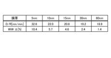
- FIG. 2 is a diagram showing an example of the relationship between the thickness and uniformity of a polymer film.
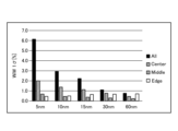
- FIG. 3 is a diagram showing an example of the relationship between the thickness and uniformity of a polymer film.
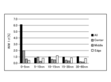
- FIG. 4 is a diagram showing an example of the relationship between the thickness and uniformity of a polymer film.
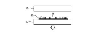
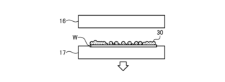
- FIG. 5A is a schematic diagram showing an example of a process for forming a polymer film.
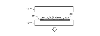
- FIG. 5B is a schematic diagram showing an example of a process for forming a polymer film.
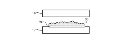
- FIG. 5C is a schematic diagram showing an example of a process for forming a polymer film.
- FIG. 5A is a schematic diagram showing an example of a process for forming a polymer film.
- FIG. 5B is a schematic diagram showing an example of a process for forming a polymer film.
- FIG. 5D is a schematic diagram showing an example of a process for forming a polymer film.
- FIG. 6 is a diagram showing an example of the uniformity when the deposition rate is changed.
- FIG. 7 is a diagram showing an example of the relationship between film thickness and uniformity in the comparative example and the embodiment.
- FIG. 8 is a diagram showing an example of the relationship between film thickness and uniformity in the comparative example and the embodiment.
- FIG. 9 is a flowchart showing an example of a film forming method.
- FIG. 10 is a diagram showing an example of the relationship between the film thickness of the polymer and the deposition rate with respect to the processing time.
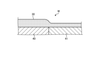
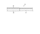
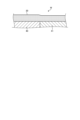
- FIG. 11 is a diagram showing an example of a film formed on surfaces with different wettability.
- FIG. 12 is a diagram showing an example of a film formed on surfaces with different wettability.
- FIG. 13 is a diagram showing an example of a film formed on surfaces with different wettability.
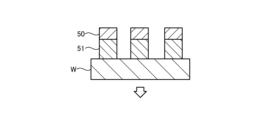
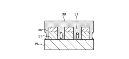
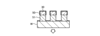
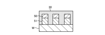
- FIG. 14A is a diagram showing an example of a process of film formation on a structure having surfaces with different wettability.
- FIG. 14B is a diagram showing an example of a process of film formation on a structure having surfaces with different wettability.
- FIG. 14C is a diagram showing an example of a process of film formation on a structure having surfaces with different wettability.
- FIG. 15A is a diagram showing an example of a process of film formation on a structure having surfaces with different wettability.
- FIG. 15B is a diagram showing an example of a process of film formation on a structure having surfaces with different wettability.
- FIG. 15C is a diagram showing an example of a process of film formation on a structure having surfaces with different wettability.
- FIG. 15D is a diagram showing an example of a process of film formation on a structure having surfaces with different wettability.
- the present disclosure therefore provides a technology that can improve the uniformity of the film thickness of a polymer formed on a substrate.
- FIG. 10 is a schematic cross-sectional view illustrating an example of a film formation apparatus 10 according to an embodiment of the present disclosure.
- the film formation apparatus 10 includes a chamber 11, an exhaust mechanism 12, a gas supply unit 13, a shower head 16, a stage 17, and a control unit 20.
- the film formation apparatus 10 is, for example, a chemical vapor deposition (CVD) apparatus.
- CVD chemical vapor deposition
- the exhaust mechanism 12 has a vacuum pump that exhausts the gas in the chamber 11, and a pressure adjustment valve that adjusts the pressure in the chamber 11.
- the inside of the chamber 11 is controlled by the exhaust mechanism 12 to a vacuum atmosphere of a predetermined pressure.
- a gas supply unit 13 that supplies multiple types of raw material monomers is connected to the chamber 11 via a shower head 16.
- the multiple types of raw material monomers are, for example, isocyanate and amine.
- Isocyanate is an example of a first monomer
- amine is an example of a second monomer.
- the gas supply unit 13 has a raw material supply source 130a, a raw material supply source 130b, a vaporizer 131a, and a vaporizer 131b.
- the raw material supply source 130a contains an isocyanate liquid.
- the raw material supply source 130b contains an amine liquid.
- the vaporizer 131a vaporizes the isocyanate liquid supplied from the raw material supply source 130a.
- the isocyanate vapor vaporized by the vaporizer 131a is introduced into the shower head 16 via the pipe 14a.
- the vaporizer 131b vaporizes the amine liquid supplied from the raw material supply source 130b.
- the amine vapor vaporized by the raw material supply source 130b is introduced into the shower head 16 via the pipe 14b.
- the shower head 16 is provided, for example, at the top of the chamber 11, and has a number of outlets formed on the bottom surface.
- the shower head 16 ejects the isocyanate vapor introduced via the pipe 14a and the amine vapor introduced via the pipe 14b in a shower-like manner from separate outlets into the chamber 11.
- a stage 17 is provided within the chamber 11.
- the stage 17 has a temperature adjustment mechanism (not shown).
- a substrate W on which a film is to be formed is placed on the stage 17.
- the substrate W has a surface made of, for example, silicon.
- the stage 17 controls the temperature of the substrate W using a temperature adjustment mechanism so that the temperature is suitable for vapor deposition polymerization of the raw material monomer supplied from the gas supply unit 13.
- the temperature suitable for vapor deposition polymerization can be determined depending on the type of raw material monomer.
- the temperature suitable for vapor deposition polymerization is, for example, within the range of 60°C to 100°C.
- a vapor deposition polymerization reaction of two types of raw material monomers occurs on the surface of the substrate W, forming a polymer film on the surface of the substrate W.
- the two types of raw material monomers are isocyanate and amine, a polyurea polymer film is deposited on the surface of the substrate W.
- the control unit 20 has a processor, a memory, and an input/output interface.
- the memory stores a program executed by the processor and a recipe including the conditions for each process.
- the processor executes the program read from the memory, and controls each part of the film forming apparatus 10 via the input/output interface based on the recipe stored in the memory, thereby performing a process for forming a polymer film on the substrate W.
- Figures 2 to 4 are diagrams showing an example of the relationship between the thickness and uniformity of a polymer film.
- Figure 4 shows the difference in uniformity between adjacent film thicknesses in Figure 3.
- film formation is continued under the same conditions until a predetermined thickness is reached.
- the film thickness uniformity improves (the values become smaller). Conversely, as the thickness of the polymer film decreases, the film thickness uniformity decreases.
- the difference in uniformity between film thicknesses of 0 nm and 5 nm is defined as the first uniformity
- the difference in uniformity between film thicknesses of 5 nm and 10 nm is defined as the second uniformity
- the difference in uniformity between film thicknesses of 10 nm and 15 nm is defined as the third uniformity
- the difference in uniformity between film thicknesses of 15 nm and 30 nm is defined as the fourth uniformity
- the difference in uniformity between film thicknesses of 30 nm and 60 nm is defined as the fifth uniformity.
- the first uniformity is the worst. There is not much difference in uniformity between the second to fifth uniformities.
- the deposition rate (D/R) decreases as the film thickness increases.
- Figures 5A to 5D are schematic diagrams showing an example of the process of forming a polymer film.
- the surface of the polymer film 30 has lower wettability (hydrophobicity) than the surface of the substrate W.
- the contact angle of the surface of silicon is approximately 31.2°
- the contact angle of the surface of the polyurea polymer film 30 is approximately 73.1°.
- the surface of the substrate W on which the polymer film 30 is formed may be a silicon nitride film, a silicon oxide film, or the like, in addition to silicon.
- the contact angle of the surface of a silicon nitride film is approximately 29.0°, and the contact angle of the surface of a silicon oxide film is approximately 50.9°.
- the surface of the substrate W is covered with a polymer film 30, and the monomer molecules are adsorbed only to the surface of the polymer film 30, as shown in Figures 5C and 5D, for example.
- the monomer molecules adsorbed to the convex parts of the surface of the polymer film 30 are easy to detach, but the monomer molecules adsorbed to the concave parts of the surface of the polymer film 30 are difficult to detach. Therefore, as the thickness of the polymer film 30 increases, the unevenness of the surface becomes less pronounced, and it is believed that the uniformity of the film thickness is further improved.
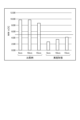
- [Relationship between deposition rate and uniformity] 6 is a diagram showing an example of uniformity when the deposition rate is changed.
- condition 1 indicates a condition in which the deposition rate is relatively low
- condition 2 indicates a condition in which the deposition rate is relatively high
- condition 3 indicates a condition in which the deposition rate is relatively high, and the deposition rate is relatively low.
- condition 1 the pressure inside the chamber 11 is set low as one of the conditions that results in a lower deposition rate than in condition 2.
- other conditions that can result in a lower deposition rate include, for example, increasing the temperature of the substrate W, lowering the flow rate of at least one type of monomer gas, and lowering the concentration of at least one type of monomer gas.
- condition 1 film formation is performed under the same conditions from the initial stage until the film thickness reaches 4.2 nm.
- condition 2 film formation is performed under the same conditions from the initial stage until the film thickness reaches 15.0 nm.
- condition 3 film formation is performed under the same conditions as condition 1 from the initial stage until the film thickness reaches 4.2 nm, and then the condition is switched to condition 2 and a further 15.0 nm of film formation is performed.
- the film thickness uniformity (WiW ⁇ [%]) is better (the value is smaller) than under condition 2, where the deposition rate is relatively high.
- the film thickness uniformity is better than that under condition 2, and is the same as that under condition 1.
- condition 3 has a higher deposition rate than condition 1, it is possible to achieve a higher throughput than condition 1 while maintaining the same uniformity as condition 1.
- condition 3 film formation is performed under conditions with a low deposition rate at the beginning of film formation, and then film formation is performed under conditions with a high deposition rate. Therefore, in this embodiment, it is possible to improve the uniformity of the film thickness, and it is possible to shorten the time required to form a polymer film of a predetermined thickness on the substrate W, compared to the case where film formation is continued under conditions with a low deposition rate.
- FIGS. 7 and 8 are diagrams showing an example of the relationship between film thickness and uniformity in a comparative example and an embodiment.
- the results of film formation under conditions of a high deposition rate are shown as a comparative example, and the results of film formation under conditions of a low deposition rate in the early stages of film formation, followed by film formation under conditions of a high deposition rate are shown as an embodiment.
- the present embodiment has better (smaller) film thickness uniformity (WiW ⁇ [%]) than the comparative example.
- the film formation method of the present embodiment can suppress the film thickness uniformity (WiW ⁇ [%]) to 5% or less.
- FIG. 9 is a flowchart showing an example of a film forming method.
- the film forming method illustrated in FIG. 9 is realized by the control unit 20 controlling each part of the film forming apparatus 10.
- step S10 the control unit 20 controls, for example, a lift pin drive mechanism (not shown) so that the tips of the lift pins (not shown) protrude from the top surface of the stage 17.
- the control unit 20 controls a gate valve (not shown) that opens and closes an opening (not shown) formed in the side wall of the chamber 11 to open the gate valve.
- the substrate W is loaded into the chamber 11 by a transfer robot (not shown) through the opening in the side wall of the chamber 11 and placed on the lift pins.
- the control unit 20 controls the lift pin drive mechanism so that the lift pins are lowered. As a result, the lift pins are lowered and the substrate W is placed on the stage 17.
- the control unit 20 then controls the gate valve to close the gate valve.
- a first film formation process is performed (step S11).
- the first film formation process in step S11 is performed under the following conditions, for example. Temperature of substrate W: 80° C. Flow rate of isocyanate vapor: 10 sccm Amine vapor flow rate: 20 sccm Pressure in chamber 11: 0.25 Torr (approximately 33.3 Pa) Flow rate of additive gas (e.g., nitrogen gas) in chamber 11: 400 sccm Processing time: 60 seconds
- the relationship between the polymer film thickness and deposition rate versus processing time in the first film formation process in step S11 is as shown, for example, in FIG. 10.
- the deposition rate is high from the start of polymer film formation until the film thickness reaches 0.6 nm, but once the film thickness exceeds this, it takes time to form the film.
- the film thickness of the polymer formed in the first film formation process is preferably 0.6 nm to 5 nm. It is preferable that the deposition rate of the polymer film in the first film formation process is, for example, 5 nm/min or less.
- a second film forming process is performed (step S12).
- the second film forming process in step S12 is performed under a condition with a lower deposition rate than the first film forming process in step S11.
- the second film forming process in step S12 is performed under the following conditions, for example. Temperature of substrate W: 80° C. Flow rate of isocyanate vapor: 10 sccm Amine vapor flow rate: 20 sccm Pressure in chamber 11: 1.0 Torr (about 133.3 Pa) Flow rate of additive gas (e.g., nitrogen gas) in chamber 11: 400 sccm Processing time: 43 seconds
- step S13 the control unit 20 controls a lift pin drive mechanism (not shown) so that the tips of the lift pins (not shown) protrude from the upper surface of the stage 17, thereby lifting the substrate W from the stage 17.
- the control unit 20 controls a gate valve (not shown) to open it, and the substrate W is removed from the chamber 11 by a transfer robot (not shown) through an opening formed in the side wall of the chamber 11.
- the control unit 20 then controls the gate valve to close it, and controls the lift pin drive mechanism so that the lift pins descend. This completes the film formation method shown in this flowchart.
- the film formation method in the embodiment includes a first film formation process and a second film formation process.
- a polymer film (film 30) is formed on the surface of a substrate (substrate W) in the chamber (chamber 11) by supplying a gas of a first monomer and a gas of a second monomer into the chamber.
- a polymer film is further formed on the polymer film formed in the first film formation process at a higher deposition rate than the first film formation process by supplying the first monomer and the second monomer into the chamber. This makes it possible to improve the uniformity of the film thickness of the polymer formed on the substrate.
- the pressure in the chamber in the first film formation process is lower than the pressure in the chamber in the second film formation process. This can improve the uniformity of the film thickness of the polymer formed on the substrate.
- the temperature of the substrate in the first film formation process is higher than the temperature of the substrate in the second film formation process. This can improve the uniformity of the film thickness of the polymer formed on the substrate.
- the flow rates of the first monomer and second monomer gases in the first film-forming process are less than the flow rates of the first monomer and second monomer gases in the second film-forming process. This can improve the uniformity of the film thickness of the polymer formed on the substrate.
- the concentrations of the first monomer and second monomer gases supplied into the chamber in the first film-forming process are lower than the concentrations of the first monomer and second monomer gases supplied into the chamber in the second film-forming process. This can improve the uniformity of the film thickness of the polymer formed on the substrate.
- the deposition rate in the first film formation process is 5 nm/min or less. This can improve the uniformity of the film thickness of the polymer formed on the substrate.
- At least a portion of the surface of the substrate is silicon, a silicon nitride film, or a silicon oxide film. This can improve the uniformity of the film thickness of the polymer formed on the substrate.
- a polymer film having a thickness of 0.6 nm to 5 nm is formed in the first film formation process. This can improve the uniformity of the polymer film thickness formed on the substrate.
- the film forming apparatus (film forming apparatus 10) in the above embodiment includes a chamber (chamber 11), a stage (stage 17), a gas supply unit (gas supply unit 13), and a control unit (control unit 20).
- the stage is provided in the chamber, and a substrate is placed on the stage.
- the gas supply unit supplies a first monomer and a second monomer gas into the chamber.
- the control unit executes a first film forming process and a second film forming process.
- the gas supply unit is controlled to supply the first monomer and the second monomer gas into the chamber, and a polymer film is formed on the surface of the substrate in the chamber.
- the gas supply unit is controlled to supply the first monomer and the second monomer into the chamber, and a polymer film is further formed on the polymer film formed in the first film forming process at a deposition rate higher than that of the first film forming process. This can improve the uniformity of the film thickness of the polymer formed on the substrate.
- a polymer film is formed on a substrate W having a silicon surface, but the disclosed technology is not limited to this.
- the disclosed technology can also be applied to the case of forming a polymer film on the surfaces of two members having surfaces with different surface wettability.
- film formation is performed under conditions where the deposition rate is low in the early stages of film formation.
- the surface of member 40 which has a highly wettable (hydrophilic) surface, is covered with a thin polymer film 30, as shown in FIG. 12, for example. Since the surface of polymer film 30 has low wettability (hydrophobicity), the surface of member 40 is covered with polymer film 30, and therefore the difference in surface wettability is reduced across the entire substrate W.
- film formation is performed under conditions where the deposition rate is high, and as shown in FIG. 13, for example, the difference in thickness between polymer film 30 formed on member 40 and polymer film 30 formed on member 41 can be reduced. This can improve the uniformity of the thickness of polymer film 30 across the entire substrate W.
- FIG. 14A a structure is formed on a substrate W, the structure having a member 50 having a surface with relatively high wettability (hydrophilic) and a member 51 having a surface with relatively low wettability (hydrophobic).
- film formation is performed under conditions of a high deposition rate, so that the thickness of the polymer film 30 can be increased in a state where the difference between the thickness of the polymer film 30 on the member 40 and the thickness of the polymer film 30 on the member 41 is small, as shown in FIG. 15C, for example.
- FIG. 15C the difference between the thickness of the polymer film 30 on the member 40 and the thickness of the polymer film 30 on the member 41 is small.
- FIG. 15C for example.
- the member 50 may be, for example, a silicon nitride film, the member 51 may be, for example, ruthenium, and the substrate W may be, for example, silicon.
- the member 50 may be, for example, a titanium nitride film, the member 51 may be, for example, a carbon-containing silicon oxide film (SiOC film), and the substrate W may be, for example, silicon.
- the contact angle of the surface of titanium nitride is approximately 56.2°
- the contact angle of the surface of a carbon-containing silicon oxide film is approximately 129.1°.
- a polymer film having a urea bond is formed on the surface of the substrate W using isocyanate as the first monomer and amine as the second monomer, but the disclosed technology is not limited to this.
- a polymer film having a 2-aminoethanol bond (-NH-CH2-CH(OH)-) may be formed on the surface of the substrate W using epoxide as the first monomer and amine as the second monomer.
- a polymer film having a urethane bond (-NH-CO-O-) may be formed on the surface of the substrate W using isocyanate as the first monomer and alcohol as the second monomer.
- a polymer film having an amide bond may be formed on the surface of the substrate W using acyl halide as the first monomer and amine as the second monomer.
- a polymer film having an imide bond may be formed on the surface of the substrate W using carboxylic anhydride as the first monomer and amine as the second monomer.
- Appendix 4 4.
- the film forming method according to claim 1, wherein a flow rate of the gas of the first monomer and the gas of the second monomer in the first film forming step is lower than a flow rate of the gas of the first monomer and the gas of the second monomer in the second film forming step.
- Appendix 5 5.
- the film formation method according to claim 1, wherein a concentration of the first monomer and the second monomer gas supplied into the chamber in the first film formation step is lower than a concentration of the first monomer and the second monomer gas supplied into the chamber in the second film formation step.
- the first monomer is a carboxylic acid anhydride; the second monomer is an amine; 9. The method for forming a film according to any one of claims 1 to 8, wherein the polymer film contains an imide bond.
- the first monomer is an epoxide; the second monomer is an amine; 9. The method for forming a film according to any one of claims 1 to 8, wherein the polymer film contains a 2-aminoethanol bond.
- Appendix 12 the first monomer is an isocyanate; the second monomer is an alcohol; 9. The method for forming a film according to any one of claims 1 to 8, wherein the polymer film contains a urethane bond.
- the first monomer is an acyl halide; the second monomer is an amine; 9. The method for forming a film according to any one of claims 1 to 8, wherein the polymer film contains an amide bond.
- Appendix 14 A chamber; a stage provided within the chamber and on which a substrate is placed; a gas supply unit that supplies a first monomer gas and a second monomer gas into the chamber; A control unit.
- the control unit is a first film formation step of supplying gases of the first monomer and the second monomer into the chamber by controlling the gas supply unit to form a polymer film on the surface of the substrate in the chamber; a second film formation process for further forming a polymer film on the polymer film formed in the first film formation process at a deposition rate higher than that of the first film formation process by supplying gases of the first monomer and the second monomer into the chamber by controlling the gas supply unit.
Landscapes
- Chemical & Material Sciences (AREA)
- Chemical Kinetics & Catalysis (AREA)
- Engineering & Computer Science (AREA)
- Materials Engineering (AREA)
- Mechanical Engineering (AREA)
- Metallurgy (AREA)
- Organic Chemistry (AREA)
- Physical Vapour Deposition (AREA)
- Formation Of Insulating Films (AREA)
Abstract
Description
図1は、本開示の一実施形態における成膜装置10の一例を示す概略断面図である。成膜装置10は、チャンバ11、排気機構12、ガス供給部13、シャワーヘッド16、ステージ17、および制御部20を有する。本実施形態において、成膜装置10は、例えばCVD(Chemical Vapor Deposition)装置である。
図2~図4は、重合体の膜の厚さと均一性の関係の一例を示す図である。図4は、図3において隣接する膜厚について均一性の差分をとったものである。図2~図4では、所定の厚さになるまで同一の条件で成膜が続けられる。
図6は、デポジションレートを変えた場合の均一性の一例を示す図である。図6において、条件1はデポジションレートが比較的低い条件を示し、条件2はデポジションレートが比較的高い条件を示している。また、条件3は、条件1の成膜に続けて条件2の成膜を行う条件である。
基板Wの温度:80℃
イソシアネートの蒸気の流量:10sccm
アミンの蒸気の流量:20sccm
チャンバ11内の圧力:0.25Torr(約33.3Pa)
チャンバ11内の添加ガス(例えば窒素ガス)の流量:400sccm
処理時間:60秒
基板Wの温度:80℃
イソシアネートの蒸気の流量:10sccm
アミンの蒸気の流量:20sccm
チャンバ11内の圧力:1.0Torr(約133.3Pa)
チャンバ11内の添加ガス(例えば窒素ガス)の流量:400sccm
処理時間:43秒
なお、本願に開示された技術は、上記した実施形態に限定されるものではなく、その要旨の範囲内で数々の変形が可能である。
チャンバ内に第1のモノマーおよび第2のモノマーのガスを供給することにより、前記チャンバ内の基板の表面に重合体の膜を形成する第1の成膜工程と、
前記チャンバ内に前記第1のモノマーおよび前記第2のモノマーを供給することにより、前記第1の成膜工程より高いデポジションレートで、前記第1の成膜工程で形成された前記重合体の膜の上に重合体の膜をさらに形成する第2の成膜工程と
を実行する成膜方法。
(付記2)
前記第1の成膜工程における前記チャンバ内の圧力は、前記第2の成膜工程における前記チャンバ内の圧力よりも低い付記1に記載の成膜方法。
(付記3)
前記第1の成膜工程における前記基板の温度は、前記第2の成膜工程における前記基板の温度よりも高い付記1または2に記載の成膜方法。
(付記4)
前記第1の成膜工程における前記第1のモノマーおよび前記第2のモノマーのガスの流量は、前記第2の成膜工程における前記第1のモノマーおよび前記第2のモノマーのガスの流量よりも少ない付記1から3のいずれか一つに記載の成膜方法。
(付記5)
前記第1の成膜工程において前記チャンバ内に供給される前記第1のモノマーおよび前記第2のモノマーのガスの濃度は、前記第2の成膜工程において前記チャンバ内に供給される前記第1のモノマーおよび前記第2のモノマーのガスの濃度よりも低い付記1から4のいずれか一つに記載の成膜方法。
(付記6)
前記第1の成膜工程におけるデポジションレートは、5nm/min以下である付記1から5のいずれか一つに記載の成膜方法。
(付記7)
前記基板の表面の少なくとも一部は、シリコン、シリコン窒化膜、またはシリコン酸化膜である付記1から6のいずれか一つに記載の成膜方法。
(付記8)
前記第1の成膜工程では、0.6nm~5nmの厚さの前記重合体の膜が形成される付記1から7のいずれか一つに記載の成膜方法。
(付記9)
前記第1のモノマーは、イソシアネートであり、
前記第2のモノマーは、アミンであり、
前記重合体の膜には尿素結合が含まれる付記1から8のいずれか一つに記載の成膜方法。
(付記10)
前記第1のモノマーは、カルボン酸無水物であり、
前記第2のモノマーは、アミンであり、
前記重合体の膜にはイミド結合が含まれる付記1から8のいずれか一つに記載の成膜方法。
(付記11)
前記第1のモノマーは、エポキシドであり、
前記第2のモノマーは、アミンであり、
前記重合体の膜には2-アミノエタノール結合が含まれる付記1から8のいずれか一つに記載の成膜方法。
(付記12)
前記第1のモノマーは、イソシアネートであり、
前記第2のモノマーは、アルコールであり、
前記重合体の膜にはウレタン結合が含まれる付記1から8のいずれか一つに記載の成膜方法。
(付記13)
前記第1のモノマーは、ハロゲン化アシルであり、
前記第2のモノマーは、アミンであり、
前記重合体の膜にはアミド結合が含まれる付記1から8のいずれか一つに記載の成膜方法。
(付記14)
チャンバと、
前記チャンバ内に設けられ、基板が載せられるステージと、
前記チャンバ内に第1のモノマーおよび第2のモノマーのガスを供給するガス供給部と、
制御部と
を備え、
前記制御部は、
前記ガス供給部を制御することにより前記チャンバ内に前記第1のモノマーおよび前記第2のモノマーのガスを供給し、前記チャンバ内の前記基板の表面に重合体の膜を形成する第1の成膜工程と、
前記ガス供給部を制御することにより前記チャンバ内に前記第1のモノマーおよび前記第2のモノマーのガスを供給することにより、前記第1の成膜工程より高いデポジションレートで、前記第1の成膜工程で形成された前記重合体の膜の上に重合体の膜をさらに形成する第2の成膜工程と
を実行する成膜装置。
10 成膜装置
11 チャンバ
12 排気機構
13 ガス供給部
130 原料供給源
131 気化器
14 配管
16 シャワーヘッド
17 ステージ
20 制御部
30 膜
31 ボイド
40 部材
41 部材
50 部材
51 部材
Claims (14)
- チャンバ内に第1のモノマーおよび第2のモノマーのガスを供給することにより、前記チャンバ内の基板の表面に重合体の膜を形成する第1の成膜工程と、
前記チャンバ内に前記第1のモノマーおよび前記第2のモノマーを供給することにより、前記第1の成膜工程より高いデポジションレートで、前記第1の成膜工程で形成された前記重合体の膜の上に重合体の膜をさらに形成する第2の成膜工程と
を実行する成膜方法。 - 前記第1の成膜工程における前記チャンバ内の圧力は、前記第2の成膜工程における前記チャンバ内の圧力よりも低い請求項1に記載の成膜方法。
- 前記第1の成膜工程における前記基板の温度は、前記第2の成膜工程における前記基板の温度よりも高い請求項1または2に記載の成膜方法。
- 前記第1の成膜工程における前記第1のモノマーおよび前記第2のモノマーのガスの流量は、前記第2の成膜工程における前記第1のモノマーおよび前記第2のモノマーのガスの流量よりも少ない請求項1または2に記載の成膜方法。
- 前記第1の成膜工程において前記チャンバ内に供給される前記第1のモノマーおよび前記第2のモノマーのガスの濃度は、前記第2の成膜工程において前記チャンバ内に供給される前記第1のモノマーおよび前記第2のモノマーのガスの濃度よりも低い請求項1または2に記載の成膜方法。
- 前記第1の成膜工程におけるデポジションレートは、5nm/min以下である請求項1または2に記載の成膜方法。
- 前記基板の表面の少なくとも一部は、シリコン、シリコン窒化膜、またはシリコン酸化膜である請求項1または2に記載の成膜方法。
- 前記第1の成膜工程では、0.6nm~5nmの厚さの前記重合体の膜が形成される請求項1または2に記載の成膜方法。
- 前記第1のモノマーは、イソシアネートであり、
前記第2のモノマーは、アミンであり、
前記重合体の膜には尿素結合が含まれる請求項1または2に記載の成膜方法。 - 前記第1のモノマーは、カルボン酸無水物であり、
前記第2のモノマーは、アミンであり、
前記重合体の膜にはイミド結合が含まれる請求項1または2に記載の成膜方法。 - 前記第1のモノマーは、エポキシドであり、
前記第2のモノマーは、アミンであり、
前記重合体の膜には2-アミノエタノール結合が含まれる請求項1または2に記載の成膜方法。 - 前記第1のモノマーは、イソシアネートであり、
前記第2のモノマーは、アルコールであり、
前記重合体の膜にはウレタン結合が含まれる請求項1または2に記載の成膜方法。 - 前記第1のモノマーは、ハロゲン化アシルであり、
前記第2のモノマーは、アミンであり、
前記重合体の膜にはアミド結合が含まれる請求項1または2に記載の成膜方法。 - チャンバと、
前記チャンバ内に設けられ、基板が載せられるステージと、
前記チャンバ内に第1のモノマーおよび第2のモノマーのガスを供給するガス供給部と、
制御部と
を備え、
前記制御部は、
前記ガス供給部を制御することにより前記チャンバ内に前記第1のモノマーおよび前記第2のモノマーのガスを供給し、前記チャンバ内の前記基板の表面に重合体の膜を形成する第1の成膜工程と、
前記ガス供給部を制御することにより前記チャンバ内に前記第1のモノマーおよび前記第2のモノマーのガスを供給することにより、前記第1の成膜工程より高いデポジションレートで、前記第1の成膜工程で形成された前記重合体の膜の上に重合体の膜をさらに形成する第2の成膜工程と
を実行する成膜装置。
Priority Applications (1)
| Application Number | Priority Date | Filing Date | Title |
|---|---|---|---|
| KR1020267013419A KR20260066191A (ko) | 2023-11-08 | 2024-10-25 | 성막 방법 및 성막 장치 |
Applications Claiming Priority (2)
| Application Number | Priority Date | Filing Date | Title |
|---|---|---|---|
| JP2023190535A JP2025078162A (ja) | 2023-11-08 | 2023-11-08 | 成膜方法および成膜装置 |
| JP2023-190535 | 2023-11-08 |
Publications (1)
| Publication Number | Publication Date |
|---|---|
| WO2025100258A1 true WO2025100258A1 (ja) | 2025-05-15 |
Family
ID=95695895
Family Applications (1)
| Application Number | Title | Priority Date | Filing Date |
|---|---|---|---|
| PCT/JP2024/038040 Pending WO2025100258A1 (ja) | 2023-11-08 | 2024-10-25 | 成膜方法および成膜装置 |
Country Status (4)
| Country | Link |
|---|---|
| JP (1) | JP2025078162A (ja) |
| KR (1) | KR20260066191A (ja) |
| TW (1) | TW202530469A (ja) |
| WO (1) | WO2025100258A1 (ja) |
Citations (3)
| Publication number | Priority date | Publication date | Assignee | Title |
|---|---|---|---|---|
| JP2013247287A (ja) * | 2012-05-28 | 2013-12-09 | Tokyo Electron Ltd | 成膜方法 |
| JP2019207965A (ja) * | 2018-05-30 | 2019-12-05 | 東京エレクトロン株式会社 | 成膜装置及び成膜方法 |
| JP2022035326A (ja) * | 2020-08-20 | 2022-03-04 | 東京エレクトロン株式会社 | 半導体装置の製造方法および成膜装置 |
-
2023
- 2023-11-08 JP JP2023190535A patent/JP2025078162A/ja active Pending
-
2024
- 2024-10-25 KR KR1020267013419A patent/KR20260066191A/ko active Pending
- 2024-10-25 WO PCT/JP2024/038040 patent/WO2025100258A1/ja active Pending
- 2024-10-30 TW TW113141468A patent/TW202530469A/zh unknown
Patent Citations (3)
| Publication number | Priority date | Publication date | Assignee | Title |
|---|---|---|---|---|
| JP2013247287A (ja) * | 2012-05-28 | 2013-12-09 | Tokyo Electron Ltd | 成膜方法 |
| JP2019207965A (ja) * | 2018-05-30 | 2019-12-05 | 東京エレクトロン株式会社 | 成膜装置及び成膜方法 |
| JP2022035326A (ja) * | 2020-08-20 | 2022-03-04 | 東京エレクトロン株式会社 | 半導体装置の製造方法および成膜装置 |
Also Published As
| Publication number | Publication date |
|---|---|
| KR20260066191A (ko) | 2026-05-12 |
| JP2025078162A (ja) | 2025-05-20 |
| TW202530469A (zh) | 2025-08-01 |
Similar Documents
| Publication | Publication Date | Title |
|---|---|---|
| US12009201B2 (en) | Method of processing substrate, method of manufacturing semiconductor device, substrate processing apparatus, and recording medium | |
| US20030029475A1 (en) | Multistep remote plasma clean process | |
| US20190309420A1 (en) | Substrate Processing Apparatus and Substrate Processing Method | |
| US20120100722A1 (en) | Substrate processing apparatus and semiconductor device manufacturing method | |
| US20180355479A1 (en) | Film forming apparatus, method of cleaning film forming apparatus, and storage medium | |
| US12381090B2 (en) | Etching method and etching apparatus | |
| US11887861B2 (en) | Substrate processing method and substrate processing apparatus | |
| US8124536B2 (en) | Manufacturing method of capacitor electrode, manufacturing system of capacitor electrode, and storage medium | |
| CN120072642A (zh) | 蚀刻方法和蚀刻装置 | |
| US12288684B2 (en) | Method of processing substrate, method of manufacturing semiconductor device, substrate processing apparatus, and recording medium | |
| KR102722064B1 (ko) | 성막 장치 및 성막 방법 | |
| KR20190079543A (ko) | 에칭 방법 및 에칭 장치 | |
| TWI842752B (zh) | 用於膜沉積及表面處理的連續電漿 | |
| US12272541B2 (en) | Etching method and etching apparatus | |
| US20220068637A1 (en) | Film-forming method, film-forming apparatus, and oxidation method | |
| JP2025078162A (ja) | 成膜方法および成膜装置 | |
| KR20230007949A (ko) | 세정 가스를 제공하기 위한 세정 가스 시스템을 갖는 화학 기상 증착 퍼니스 | |
| TWI856606B (zh) | 高壓基板處理裝置以及利用所述處理裝置的基板用高壓化學氣相沉積方法 | |
| JP7210647B2 (ja) | 薄膜蒸着方法及びこれを用いた半導体素子の製造方法 | |
| US12620565B2 (en) | Substrate processing apparatus | |
| JP7822166B2 (ja) | ガス処理方法およびガス処理装置 | |
| US20240150500A1 (en) | Substrate processing apparatus | |
| US20240200193A1 (en) | Method of performing cleaning and apparatus for performing substrate processing | |
| KR20230165047A (ko) | 기판 처리 장치를 이용한 기판 처리 방법 | |
| KR20190070858A (ko) | 실리콘 함유막의 에칭 방법, 컴퓨터 기억 매체, 및 실리콘 함유막의 에칭 장치 |
Legal Events
| Date | Code | Title | Description |
|---|---|---|---|
| 121 | Ep: the epo has been informed by wipo that ep was designated in this application |
Ref document number: 24888555 Country of ref document: EP Kind code of ref document: A1 |
|
| ENP | Entry into the national phase |
Ref document number: 1020267013419 Country of ref document: KR Free format text: ST27 STATUS EVENT CODE: A-0-1-A10-A15-NAP-PA0105 (AS PROVIDED BY THE NATIONAL OFFICE) |
|
| WWE | Wipo information: entry into national phase |
Ref document number: 1020267013419 Country of ref document: KR |
|
| WWP | Wipo information: published in national office |
Ref document number: 1020267013419 Country of ref document: KR |
|
| NENP | Non-entry into the national phase |
Ref country code: DE |