WO2025069652A1 - プラズマ処理装置 - Google Patents
プラズマ処理装置 Download PDFInfo
- Publication number
- WO2025069652A1 WO2025069652A1 PCT/JP2024/025501 JP2024025501W WO2025069652A1 WO 2025069652 A1 WO2025069652 A1 WO 2025069652A1 JP 2024025501 W JP2024025501 W JP 2024025501W WO 2025069652 A1 WO2025069652 A1 WO 2025069652A1
- Authority
- WO
- WIPO (PCT)
- Prior art keywords
- electrode
- plasma processing
- electrically connected
- signal
- processing apparatus
- Prior art date
- Legal status (The legal status is an assumption and is not a legal conclusion. Google has not performed a legal analysis and makes no representation as to the accuracy of the status listed.)
- Ceased
Links
Images









Classifications
-
- H—ELECTRICITY
- H01—ELECTRIC ELEMENTS
- H01J—ELECTRIC DISCHARGE TUBES OR DISCHARGE LAMPS
- H01J37/00—Discharge tubes with provision for introducing objects or material to be exposed to the discharge, e.g. for the purpose of examination or processing thereof
- H01J37/32—Gas-filled discharge tubes
- H01J37/32431—Constructional details of the reactor
- H01J37/32532—Electrodes
- H01J37/32577—Electrical connecting means
-
- H—ELECTRICITY
- H01—ELECTRIC ELEMENTS
- H01J—ELECTRIC DISCHARGE TUBES OR DISCHARGE LAMPS
- H01J37/00—Discharge tubes with provision for introducing objects or material to be exposed to the discharge, e.g. for the purpose of examination or processing thereof
- H01J37/32—Gas-filled discharge tubes
- H01J37/32009—Arrangements for generation of plasma specially adapted for examination or treatment of objects, e.g. plasma sources
- H01J37/32082—Radio frequency generated discharge
- H01J37/32174—Circuits specially adapted for controlling the RF discharge
- H01J37/32183—Matching circuits
-
- H—ELECTRICITY
- H01—ELECTRIC ELEMENTS
- H01J—ELECTRIC DISCHARGE TUBES OR DISCHARGE LAMPS
- H01J37/00—Discharge tubes with provision for introducing objects or material to be exposed to the discharge, e.g. for the purpose of examination or processing thereof
- H01J37/32—Gas-filled discharge tubes
- H01J37/32009—Arrangements for generation of plasma specially adapted for examination or treatment of objects, e.g. plasma sources
- H01J37/32018—Glow discharge
- H01J37/32027—DC powered
-
- H—ELECTRICITY
- H01—ELECTRIC ELEMENTS
- H01J—ELECTRIC DISCHARGE TUBES OR DISCHARGE LAMPS
- H01J37/00—Discharge tubes with provision for introducing objects or material to be exposed to the discharge, e.g. for the purpose of examination or processing thereof
- H01J37/32—Gas-filled discharge tubes
- H01J37/32009—Arrangements for generation of plasma specially adapted for examination or treatment of objects, e.g. plasma sources
- H01J37/32082—Radio frequency generated discharge
- H01J37/32091—Radio frequency generated discharge the radio frequency energy being capacitively coupled to the plasma
-
- H—ELECTRICITY
- H01—ELECTRIC ELEMENTS
- H01J—ELECTRIC DISCHARGE TUBES OR DISCHARGE LAMPS
- H01J37/00—Discharge tubes with provision for introducing objects or material to be exposed to the discharge, e.g. for the purpose of examination or processing thereof
- H01J37/32—Gas-filled discharge tubes
- H01J37/32009—Arrangements for generation of plasma specially adapted for examination or treatment of objects, e.g. plasma sources
- H01J37/32082—Radio frequency generated discharge
- H01J37/32128—Radio frequency generated discharge using particular waveforms, e.g. polarised waves
-
- H—ELECTRICITY
- H01—ELECTRIC ELEMENTS
- H01J—ELECTRIC DISCHARGE TUBES OR DISCHARGE LAMPS
- H01J37/00—Discharge tubes with provision for introducing objects or material to be exposed to the discharge, e.g. for the purpose of examination or processing thereof
- H01J37/32—Gas-filled discharge tubes
- H01J37/32009—Arrangements for generation of plasma specially adapted for examination or treatment of objects, e.g. plasma sources
- H01J37/32082—Radio frequency generated discharge
- H01J37/32137—Radio frequency generated discharge controlling of the discharge by modulation of energy
- H01J37/32146—Amplitude modulation, includes pulsing
-
- H—ELECTRICITY
- H01—ELECTRIC ELEMENTS
- H01J—ELECTRIC DISCHARGE TUBES OR DISCHARGE LAMPS
- H01J37/00—Discharge tubes with provision for introducing objects or material to be exposed to the discharge, e.g. for the purpose of examination or processing thereof
- H01J37/32—Gas-filled discharge tubes
- H01J37/32009—Arrangements for generation of plasma specially adapted for examination or treatment of objects, e.g. plasma sources
- H01J37/32082—Radio frequency generated discharge
- H01J37/32137—Radio frequency generated discharge controlling of the discharge by modulation of energy
- H01J37/32155—Frequency modulation
- H01J37/32165—Plural frequencies
-
- H—ELECTRICITY
- H01—ELECTRIC ELEMENTS
- H01J—ELECTRIC DISCHARGE TUBES OR DISCHARGE LAMPS
- H01J37/00—Discharge tubes with provision for introducing objects or material to be exposed to the discharge, e.g. for the purpose of examination or processing thereof
- H01J37/32—Gas-filled discharge tubes
- H01J37/32009—Arrangements for generation of plasma specially adapted for examination or treatment of objects, e.g. plasma sources
- H01J37/32082—Radio frequency generated discharge
- H01J37/32174—Circuits specially adapted for controlling the RF discharge
-
- H—ELECTRICITY
- H01—ELECTRIC ELEMENTS
- H01J—ELECTRIC DISCHARGE TUBES OR DISCHARGE LAMPS
- H01J37/00—Discharge tubes with provision for introducing objects or material to be exposed to the discharge, e.g. for the purpose of examination or processing thereof
- H01J37/32—Gas-filled discharge tubes
- H01J37/32431—Constructional details of the reactor
- H01J37/32532—Electrodes
- H01J37/32568—Relative arrangement or disposition of electrodes; moving means
-
- H—ELECTRICITY
- H01—ELECTRIC ELEMENTS
- H01J—ELECTRIC DISCHARGE TUBES OR DISCHARGE LAMPS
- H01J37/00—Discharge tubes with provision for introducing objects or material to be exposed to the discharge, e.g. for the purpose of examination or processing thereof
- H01J37/32—Gas-filled discharge tubes
- H01J37/32431—Constructional details of the reactor
- H01J37/32697—Electrostatic control
- H01J37/32706—Polarising the substrate
-
- H—ELECTRICITY
- H01—ELECTRIC ELEMENTS
- H01J—ELECTRIC DISCHARGE TUBES OR DISCHARGE LAMPS
- H01J37/00—Discharge tubes with provision for introducing objects or material to be exposed to the discharge, e.g. for the purpose of examination or processing thereof
- H01J37/32—Gas-filled discharge tubes
- H01J37/32431—Constructional details of the reactor
- H01J37/32715—Workpiece holder
-
- H—ELECTRICITY
- H05—ELECTRIC TECHNIQUES NOT OTHERWISE PROVIDED FOR
- H05H—PLASMA TECHNIQUE; PRODUCTION OF ACCELERATED ELECTRICALLY-CHARGED PARTICLES OR OF NEUTRONS; PRODUCTION OR ACCELERATION OF NEUTRAL MOLECULAR OR ATOMIC BEAMS
- H05H1/00—Generating plasma; Handling plasma
- H05H1/24—Generating plasma
- H05H1/46—Generating plasma using applied electromagnetic fields, e.g. high frequency or microwave energy
-
- H—ELECTRICITY
- H01—ELECTRIC ELEMENTS
- H01J—ELECTRIC DISCHARGE TUBES OR DISCHARGE LAMPS
- H01J37/00—Discharge tubes with provision for introducing objects or material to be exposed to the discharge, e.g. for the purpose of examination or processing thereof
- H01J37/32—Gas-filled discharge tubes
- H01J37/32431—Constructional details of the reactor
- H01J37/32532—Electrodes
-
- H—ELECTRICITY
- H01—ELECTRIC ELEMENTS
- H01J—ELECTRIC DISCHARGE TUBES OR DISCHARGE LAMPS
- H01J37/00—Discharge tubes with provision for introducing objects or material to be exposed to the discharge, e.g. for the purpose of examination or processing thereof
- H01J37/32—Gas-filled discharge tubes
- H01J37/32431—Constructional details of the reactor
- H01J37/32623—Mechanical discharge control means
- H01J37/32642—Focus rings
Definitions
- An exemplary embodiment of the present disclosure relates to a plasma processing apparatus.
- Patent Document 1 discloses a DC power supply for applying a negative DC voltage to an upper electrode.
- Patent Document 2 discloses a voltage pulse generator for applying a negative voltage pulse to a bias electrode of a substrate support.
- This disclosure provides a technique for stabilizing plasma.
- a plasma processing apparatus in one exemplary embodiment of the present disclosure, includes a chamber, a substrate support disposed within the chamber and including at least one lower electrode, an upper electrode disposed above the substrate support, an RF signal generator electrically connected to either the at least one lower electrode or the upper electrode and configured to generate an RF signal to generate a plasma in the chamber, a first voltage signal generator electrically connected to either the at least one lower electrode and configured to generate a first voltage signal, the first voltage signal having a sequence of first voltage pulses, a second voltage signal generator electrically connected to the upper electrode and configured to generate a second voltage signal, a capacitor, and a rectifying element including a first electrode and a second electrode, the first electrode being electrically connected to a node between the upper electrode and the second voltage signal generator, and the second electrode being electrically connected to a ground potential via the capacitor.
- a technique for stabilizing plasma can be provided.
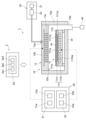
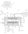
- FIG. 1 is a diagram for explaining a configuration example of a plasma processing system.
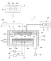
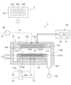
- FIG. 1 is a diagram for explaining a configuration example of a capacitively coupled plasma processing apparatus.
- 2 is a diagram showing an example of coupling between a power supply 30 and a chamber 10.
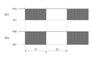
- FIG. 4 is a timing chart showing an example of voltage waveforms of a first DC signal and a second DC signal.
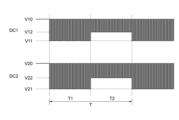
- 4 is a timing chart showing an example of voltage waveforms of a first DC signal and a second DC signal.
- 4 is a timing chart showing an example of voltage waveforms of a first DC signal and a second DC signal.
- 4 is a timing chart showing an example of voltage waveforms of a first DC signal and a second DC signal.
- FIG. 1 is a diagram for explaining a configuration example of a plasma processing system.
- FIG. 1 is a diagram for explaining a configuration example of a capacitively coupled plasma processing apparatus.
- 2 is a diagram showing an example of coupling between a power supply
- FIG. 2 is a diagram illustrating a configuration example of a plasma stabilization circuit according to the first embodiment.
- FIG. 4 illustrates an example of a first filter.
- FIG. 13 illustrates an example of a second filter.
- FIG. 13 is a diagram illustrating another example of the arrangement of the node N1.
- FIG. 13 is a diagram illustrating another example of the arrangement of the node N1.
- 4 is a diagram for explaining the operation of the plasma stabilization circuit 70.
- FIG. 4 is a diagram for explaining the operation of the plasma stabilization circuit 70.
- FIG. 4 is a diagram for explaining the rectification action of the first rectifying element D1.
- FIG. 4 is a diagram for explaining the rectification action of the first rectifying element D1.
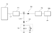
- FIG. 13 is a diagram illustrating a configuration example of a plasma stabilization circuit according to a second embodiment.
- FIG. 4 is a diagram illustrating an example of a second rectifying element.
- FIG. 4 is a diagram illustrating an example of a second rectifying element.
- 13 is a diagram showing another example of the connection between the power supply 30 and the chamber 10.
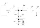
- FIG. 13 is a diagram illustrating a configuration example of a plasma stabilization circuit according to a third embodiment.
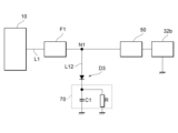
- FIG. 13 is a diagram illustrating a modified example of the first embodiment.
- FIG. 13 is a diagram illustrating a modified example of the second embodiment.
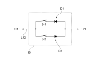
- FIG. 4 is a diagram illustrating an example of a polarity switching circuit.
- 13 is a diagram showing another example of the connection between the power supply 30 and the chamber 10.
- FIG. 13 is a diagram showing another example of the connection between the power supply 30 and the chamber 10.
- FIG. 13 is a diagram showing another example of the connection between the power supply 30 and the chamber 10.
- a plasma processing apparatus in one exemplary embodiment, includes a chamber, a substrate support disposed within the chamber and including at least one lower electrode, an upper electrode disposed above the substrate support, an RF signal generator electrically connected to either the at least one lower electrode or the upper electrode and configured to generate an RF signal to generate a plasma in the chamber, a first voltage signal generator electrically connected to either the at least one lower electrode and configured to generate a first voltage signal, the first voltage signal having a sequence of first voltage pulses, a second voltage signal generator electrically connected to the upper electrode and configured to generate a second voltage signal, a capacitor, and a rectifying element including a first electrode and a second electrode, the first electrode being electrically connected to a node between the upper electrode and the second voltage signal generator, and the second electrode being electrically connected to a ground potential via the capacitor.
- the second voltage signal has a sequence of second voltage pulses.
- the second voltage signal has a constant voltage level.
- the second voltage signal has a negative polarity
- the first electrode is a cathode electrode
- the second electrode is an anode electrode
- the first sequence of voltage pulses has a first pulse frequency in the range of 0.1 MHz to 2 MHz.
- the second sequence of voltage pulses has a second pulse frequency in the range of 0.1 kHz to 50 kHz.
- the device further includes a filter circuit provided in the transmission line between the upper electrode and the second voltage signal generator.
- the device further includes a filter circuit provided in the transmission line between the upper electrode and the node.
- the device further includes a filter circuit disposed in the transmission line between the node and the second voltage signal generator.
- the device further includes a first filter provided in a transmission line between the upper electrode and the node and configured to filter signals in a band of an RF frequency of the RF signal, and a second filter provided in a transmission line between the node and the second voltage signal generator and configured to filter signals in a band of a pulse frequency of the sequence of first voltage pulses.
- a plasma processing apparatus in one exemplary embodiment, includes a chamber, a substrate support disposed within the chamber and including at least one lower electrode, an upper electrode disposed above the substrate support, an RF signal generator electrically connected to either the at least one lower electrode or the upper electrode and configured to generate an RF signal to generate a plasma in the chamber, a voltage signal generator electrically connected to either the at least one lower electrode and configured to generate a voltage signal, the voltage signal having a sequence of voltage pulses, an impedance fixing circuit electrically connected to the upper electrode, a capacitor, and a rectifying element including a first electrode and a second electrode, the first electrode being electrically connected to a node between the upper electrode and the impedance fixing circuit, and the second electrode being electrically connected to a ground potential via the capacitor.
- the voltage pulse has a negative polarity
- the first electrode is a cathode electrode
- the second electrode is an anode electrode
- the sequence of voltage pulses has a first pulse frequency in the range of 0.1 MHz to 2 MHz.
- the impedance fixing circuit includes at least one of a capacitor and an inductor.
- a plasma processing apparatus in one exemplary embodiment, includes a chamber, a substrate support disposed within the chamber and including an electrode, a first voltage signal generator electrically connected to the electrode and configured to generate a first voltage signal, the first voltage signal having a sequence of first voltage pulses, and a rectifying element that forms part of the chamber or is disposed within the chamber, the rectifying element including a conductive member, a capacitor, and a first electrode and a second electrode, the first electrode being electrically connected to the conductive member and the second electrode being electrically connected to a ground potential via the capacitor.
- the device further includes a second voltage signal generator electrically connected to a node between the conductive member and the first electrode of the rectifying element and configured to generate a second voltage signal.
- the device further includes an impedance fixing circuit electrically connected to a node between the conductive member and the first electrode of the rectifying element.
- the impedance fixing circuit includes at least one of a capacitor and an inductor.
- the conductive member is any one of: (a) an upper electrode disposed above the substrate support; (b) a ring assembly disposed on the substrate support so as to surround the substrate on the substrate support; (c) a liner disposed along the inner wall of the chamber; and (d) a baffle plate disposed to surround the substrate support.
- FIG. 1 is a diagram for explaining a configuration example of a plasma processing system.
- the plasma processing system includes a plasma processing device 1 and a control unit 2.
- the plasma processing system is an example of a substrate processing system
- the plasma processing device 1 is an example of a substrate processing device.
- the plasma processing device 1 includes a plasma processing chamber 10, a substrate support unit 11, and a plasma generation unit 12.
- the plasma processing chamber 10 has a plasma processing space.
- the plasma processing chamber 10 also has at least one gas supply port for supplying at least one processing gas to the plasma processing space, and at least one gas exhaust port for exhausting gas from the plasma processing space.
- the gas supply port is connected to a gas supply unit 20 described later, and the gas exhaust port is connected to an exhaust system 40 described later.
- the substrate support unit 11 is disposed in the plasma processing space, and has a substrate support surface for supporting a substrate.
- the plasma generating unit 12 is configured to generate plasma from at least one processing gas supplied into the plasma processing space.
- the plasma formed in the plasma processing space may be capacitively coupled plasma (CCP), inductively coupled plasma (ICP), electron-cyclotron-resonance plasma (ECR plasma), helicon wave plasma (HWP), or surface wave plasma (SWP), etc.
- various types of plasma generating units may be used, including AC (Alternating Current) plasma generating units and DC (Direct Current) plasma generating units.
- the AC signal (AC power) used in the AC plasma generating unit has a frequency in the range of 100 kHz to 10 GHz.
- AC signals include RF (Radio Frequency) signals and microwave signals.
- the RF signal has a frequency in the range of 100 kHz to 150 MHz.
- the control unit 2 processes computer-executable instructions that cause the plasma processing apparatus 1 to perform the various steps described in this disclosure.
- the control unit 2 may be configured to control each element of the plasma processing apparatus 1 to perform the various steps described herein. In one embodiment, a part or all of the control unit 2 may be included in the plasma processing apparatus 1.
- the control unit 2 may include a processing unit 2a1, a storage unit 2a2, and a communication interface 2a3.
- the control unit 2 is realized, for example, by a computer 2a.
- the processing unit 2a1 may be configured to perform various control operations by reading a program from the storage unit 2a2 and executing the read program. This program may be stored in the storage unit 2a2 in advance, or may be acquired via a medium when necessary.
- the acquired program is stored in the storage unit 2a2 and is read from the storage unit 2a2 by the processing unit 2a1 and executed.
- the medium may be various storage media readable by the computer 2a, or may be a communication line connected to the communication interface 2a3.
- the processing unit 2a1 may be a CPU (Central Processing Unit).
- the memory unit 2a2 may include a RAM (Random Access Memory), a ROM (Read Only Memory), a HDD (Hard Disk Drive), a SSD (Solid State Drive), or a combination of these.
- the communication interface 2a3 may communicate with the plasma processing device 1 via a communication line such as a LAN (Local Area Network).
- FIG. 1 is a diagram for explaining an example of the configuration of a capacitively coupled plasma processing device.
- the capacitively coupled plasma processing apparatus 1 includes a plasma processing chamber 10, a gas supply unit 20, a power supply 30, and an exhaust system 40.
- the plasma processing apparatus 1 also includes a substrate support unit 11 and a gas inlet unit.
- the gas inlet unit is configured to introduce at least one processing gas into the plasma processing chamber 10.
- the gas inlet unit includes a shower head 13.
- the substrate support unit 11 is disposed in the plasma processing chamber 10.
- the shower head 13 is disposed above the substrate support unit 11. In one embodiment, the shower head 13 constitutes at least a part of the ceiling of the plasma processing chamber 10.
- the plasma processing chamber 10 has a plasma processing space 10s defined by the shower head 13, the sidewall 10a of the plasma processing chamber 10, and the substrate support unit 11.
- the plasma processing chamber 10 is grounded.
- the shower head 13 and the substrate support unit 11 are electrically insulated from the housing of the plasma processing chamber 10.
- the substrate support 11 includes a main body 111 and a ring assembly 112.
- the main body 111 has a central region 111a for supporting the substrate W and an annular region 111b for supporting the ring assembly 112.
- a wafer is an example of a substrate W.
- the annular region 111b of the main body 111 surrounds the central region 111a of the main body 111 in a plan view.
- the substrate W is disposed on the central region 111a of the main body 111
- the ring assembly 112 is disposed on the annular region 111b of the main body 111 so as to surround the substrate W on the central region 111a of the main body 111. Therefore, the central region 111a is also called a substrate support surface for supporting the substrate W, and the annular region 111b is also called a ring support surface for supporting the ring assembly 112.
- the main body 111 includes a base 1110 and an electrostatic chuck 1111.
- the base 1110 includes a conductive member.
- the conductive member of the base 1110 may function as a lower electrode.
- the electrostatic chuck 1111 is disposed on the base 1110.
- the electrostatic chuck 1111 includes a ceramic member 1111a and an electrostatic electrode 1111b disposed within the ceramic member 1111a.
- the ceramic member 1111a has a central region 111a. In one embodiment, the ceramic member 1111a also has an annular region 111b. Note that other members surrounding the electrostatic chuck 1111, such as an annular electrostatic chuck or an annular insulating member, may have the annular region 111b.
- the ring assembly 112 may be disposed on the annular electrostatic chuck or the annular insulating member, or may be disposed on both the electrostatic chuck 1111 and the annular insulating member.
- at least one RF/DC electrode coupled to an RF power source 31 and/or a DC power source 32 described later may be disposed in the ceramic member 1111a.
- the at least one RF/DC electrode functions as a lower electrode.
- the RF/DC electrode is also called a bias electrode.
- the conductive member of the base 1110 and the at least one RF/DC electrode may function as multiple lower electrodes.
- the electrostatic electrode 1111b may function as a lower electrode.
- the substrate support 11 includes at least one lower electrode.
- the ring assembly 112 includes one or more annular members.
- the one or more annular members include one or more edge rings and at least one cover ring.
- the edge rings are formed of a conductive or insulating material, and the cover rings are formed of an insulating material.
- the substrate support 11 may also include a temperature adjustment module configured to adjust at least one of the electrostatic chuck 1111, the ring assembly 112, and the substrate to a target temperature.
- the temperature adjustment module may include a heater, a heat transfer medium, a flow passage 1110a, or a combination thereof.
- a heat transfer fluid such as brine or a gas flows through the flow passage 1110a.
- the flow passage 1110a is formed in the base 1110, and one or more heaters are disposed in the ceramic member 1111a of the electrostatic chuck 1111.
- the substrate support 11 may also include a heat transfer gas supply configured to supply a heat transfer gas to a gap between the back surface of the substrate W and the central region 111a.
- the shower head 13 is configured to introduce at least one processing gas from the gas supply unit 20 into the plasma processing space 10s.
- the shower head 13 has at least one gas supply port 13a, at least one gas diffusion chamber 13b, and multiple gas inlets 13c.
- the processing gas supplied to the gas supply port 13a passes through the gas diffusion chamber 13b and is introduced into the plasma processing space 10s from the multiple gas inlets 13c.
- the shower head 13 also includes at least one upper electrode.
- the gas introduction unit may include, in addition to the shower head 13, one or more side gas injectors (SGI) attached to one or more openings formed in the sidewall 10a.
- SGI side gas injectors
- the gas supply unit 20 may include at least one gas source 21 and at least one flow controller 22.
- the gas supply unit 20 is configured to supply at least one process gas from a respective gas source 21 through a respective flow controller 22 to the showerhead 13.
- Each flow controller 22 may include, for example, a mass flow controller or a pressure-controlled flow controller.
- the gas supply unit 20 may include at least one flow modulation device that modulates or pulses the flow rate of the at least one process gas.
- the power supply 30 includes an RF power supply 31 coupled to the plasma processing chamber 10 via at least one impedance matching circuit.
- the RF power supply 31 is configured to supply at least one RF signal (RF power) to at least one lower electrode and/or at least one upper electrode. This causes a plasma to be formed from at least one processing gas supplied to the plasma processing space 10s.
- the RF power supply 31 can function as at least a part of the plasma generating unit 12.
- a bias RF signal to at least one lower electrode, a bias potential is generated on the substrate W, and ion components in the formed plasma can be attracted to the substrate W.
- the RF power supply 31 includes a first RF generating unit 31a and a second RF generating unit 31b.
- the first RF generating unit 31a is coupled to at least one lower electrode and/or at least one upper electrode via at least one impedance matching circuit and configured to generate a source RF signal (source RF power) for plasma generation.
- the source RF signal has a frequency in the range of 10 MHz to 150 MHz.
- the first RF generating unit 31a may be configured to generate multiple source RF signals having different frequencies. The generated one or more source RF signals are supplied to at least one lower electrode and/or at least one upper electrode.
- the second RF generator 31b is coupled to at least one lower electrode via at least one impedance matching circuit and configured to generate a bias RF signal (bias RF power).
- the frequency of the bias RF signal may be the same as or different from the frequency of the source RF signal.
- the bias RF signal has a lower frequency than the frequency of the source RF signal.
- the bias RF signal has a frequency in the range of 100 kHz to 60 MHz.
- the second RF generator 31b may be configured to generate multiple bias RF signals having different frequencies.
- the generated one or more bias RF signals are provided to at least one lower electrode. Also, in various embodiments, at least one of the source RF signal and the bias RF signal may be pulsed.
- the power supply 30 may also include a DC power supply 32 coupled to the plasma processing chamber 10.
- the DC power supply 32 includes a first DC generator 32a and a second DC generator 32b.
- the first DC generator 32a is connected to at least one lower electrode and configured to generate a first DC signal.
- the generated first DC signal is applied to the at least one lower electrode.
- the second DC generator 32b is connected to at least one upper electrode and configured to generate a second DC signal.
- the generated second DC signal is applied to the at least one upper electrode.
- the first and second DC signals may be pulsed.
- a sequence of voltage pulses is applied to at least one lower electrode and/or at least one upper electrode.
- the voltage pulses may have a rectangular, trapezoidal, triangular or combination thereof pulse waveform.
- a waveform generator for generating a sequence of voltage pulses from the DC signal is connected between the first DC generator 32a and at least one lower electrode.
- the first DC generator 32a and the waveform generator constitute a voltage pulse generator.
- the second DC generator 32b and the waveform generator constitute a voltage pulse generator
- the voltage pulse generator is connected to at least one upper electrode.
- the voltage pulses may have a positive polarity or a negative polarity.
- the sequence of voltage pulses may also include one or more positive polarity voltage pulses and one or more negative polarity voltage pulses within one period.
- the first and second DC generating units 32a and 32b may be provided in addition to the RF power source 31, or the first DC generating unit 32a may be provided in place of the second RF generating unit 31b.
- the exhaust system 40 may be connected to, for example, a gas exhaust port 10e provided at the bottom of the plasma processing chamber 10.
- the exhaust system 40 may include a pressure regulating valve and a vacuum pump. The pressure in the plasma processing space 10s is adjusted by the pressure regulating valve.
- the vacuum pump may include a turbomolecular pump, a dry pump, or a combination thereof.
- FIG. 3 is a diagram showing an example of a connection between the power supply 30 of the plasma processing apparatus 1 and the plasma processing chamber 10 (hereinafter also referred to as "chamber 10").
- the first RF generating unit 31a is electrically connected to the lower electrode of the substrate support unit 11 via the transmission line L2. Note that one or more lower electrodes may be provided on the substrate support unit 11. When multiple lower electrodes are provided, the first RF generating unit 31a may be electrically connected to any one of the multiple lower electrodes. At least one impedance matching circuit is provided on the transmission line L2.
- the first RF generating unit 31a is configured to generate a source RF signal for plasma generation.
- the source RF signal has a frequency in the range of 10 MHz to 150 MHz.
- the first RF generating unit 31a may be configured to generate multiple source RF signals having different frequencies.
- the first RF generating unit 31a may be electrically connected to the upper electrode via at least one impedance matching circuit.
- only one lower electrode may be provided on the substrate support unit (i.e., multiple lower electrodes do not need to be provided on the substrate support unit).
- the first DC generating unit 32a is electrically connected to the lower electrode of the substrate support 11 via a transmission line L3.
- the first DC generating unit 32a may be electrically connected to the same lower electrode as the first RF generating unit 31a, or may be electrically connected to a lower electrode different from the first RF generating unit 31a.
- the first DC generating unit 32a is configured to generate a first DC signal.
- the first DC signal may be pulsed.
- a first waveform generating unit may be provided on the output side (lower electrode side) of the first DC generating unit 32a.
- the first waveform generating unit generates a sequence of first voltage pulses from the first DC signal.
- a first voltage signal having the sequence of first voltage pulses may be applied to the lower electrode.
- the first voltage pulses may have a pulse waveform that is rectangular, trapezoidal, triangular, or a combination thereof.
- the first waveform generating unit may be provided integrally within the first DC generating unit 32a.
- the first DC signal may not be pulsed.
- the first DC signal may have a constant voltage level, and the first DC signal having the constant voltage level may be applied to the lower electrode.
- the second DC generating unit 32b is electrically connected to the upper electrode of the shower head 13 via a transmission line L1.
- the second DC generating unit 32b is configured to generate a second DC signal.
- a rectifying element that limits the direction of the current is provided on the transmission line L1 between the second DC generating unit 32b and the upper electrode. Each component of the transmission line L1, including the rectifying element, will be described later.
- the second DC signal may be pulsed.
- a second waveform generating unit may be provided on the transmission line L1 on the output side (upper electrode side) of the second DC generating unit 32b.
- the second waveform generating unit generates a sequence of second voltage pulses from the second DC signal.
- the second DC signal having the sequence of second voltage pulses may be applied to the upper electrode.
- the second voltage pulses may have a pulse waveform that is rectangular, trapezoidal, triangular, or a combination thereof.
- the second waveform generating unit may be provided integrally within the second DC generating unit 32b.
- the second DC signal may not be pulsed.
- the second DC signal may have a constant voltage level and the second DC signal having the constant voltage level may be applied to the upper electrode.
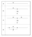
- first DC signal and second DC signal> 4A to 4D are timing charts showing examples of voltage waveforms of the first DC signal and the second DC signal.
- the voltage waveforms of the first DC signal and the second DC signal may be repeated multiple times with a repetition period T (see FIGS. 4A to 4D).
- the first DC signal may have a repetition frequency (1/T) of 0.1 kHz to 50 kHz.
- the second DC signal may have a repetition frequency (1/T) of 0.1 kHz to 50 kHz.
- the repetition frequency of the first DC signal and the repetition frequency of the second DC signal may be the same or different.
- the first DC signal and the second DC signal may be synchronous (see FIGS. 4A to 4C) or may not be synchronous.
- the first DC signal and the second DC signal may be out of phase with each other by a given value (180 degrees in one example).
- FIG. 4A is an example in which the first DC signal (DC1) and the second DC signal (DC2) are both pulsed.
- the first DC signal and the second DC signal may be generated by a first waveform generating unit and a second waveform generating unit, respectively.
- the first DC signal has a sequence of first voltage pulses having a first voltage level V11 during a first period T1 in the repeating period T.
- the sequence of first voltage pulses may have a pulse frequency of 0.1 MHz to 2 MHz (hereinafter, voltage pulses with such a pulse frequency are also referred to as "high-speed pulses").
- the first DC signal has a reference voltage level V10 during a second period T2 in the repeating period T.
- the absolute value of the reference voltage level V10 is smaller than the absolute value of the first voltage level V11.
- the first voltage level V11 has a negative polarity.
- the reference voltage level V10 has a zero voltage level.
- the second DC signal has a second sequence of voltage pulses having a second voltage level V21 during the first period T1.
- the second sequence of voltage pulses may have a pulse frequency of 0.1 MHz to 2 MHz.
- the pulse frequency of the second sequence of voltage pulses may be the same as or different from the pulse frequency of the first sequence of voltage pulses.
- the second DC signal also has a reference voltage level V20 during the second period T2.
- the reference voltage level V20 is less than the absolute value of the second voltage level V21.
- the second voltage level V21 has a negative polarity.
- the reference voltage level V20 has a zero voltage level.
- the first DC signal (DC1) and the second DC signal (DC2) may be generated in a first waveform generating unit and a second waveform generating unit, respectively. Both the first DC signal and the second DC signal are pulsed.
- the first DC signal has a sequence of third voltage pulses having a third voltage level V12 during a second period T2 in the repetition period T.
- the absolute value of the third voltage level V12 is greater than the absolute value of the reference voltage level V10 and less than the absolute value of the first voltage level V11.
- the sequence of third voltage pulses may have a pulse frequency of 0.1 MHz to 2 MHz.
- the second DC signal has a sequence of fourth voltage pulses having a fourth voltage level V22 during a second period T2 in the repetition period T.
- the absolute value of the fourth voltage level V22 is greater than the absolute value of the reference voltage level V20 and less than the absolute value of the second voltage level V21.
- the fourth voltage pulse sequence may have a pulse frequency of 0.1 MHz to 2 MHz.
- the repeating period T may further have a third period T3.
- the first DC signal may have the reference voltage level V10 during the third period T3 in the repeating period T.
- the second DC signal may have the reference voltage level V20 during the third period T3 in the repeating period T.
- the fourth DC signal is a modified example of the voltage waveform shown in FIG. 4A.
- Both the first DC signal (DC1) and the second DC signal (DC2) are pulsed.
- the first DC signal may be generated by the first waveform generating unit.
- the second DC signal may be generated by the second waveform generating unit (including the case where it is configured integrally with the second DC generating unit 32b), or may be generated by the second DC generating unit 32b.
- the second DC signal has a sequence of second voltage pulses in a repetition period T. That is, the sequence of second voltage pulses in this example has a second voltage level V21 during the first period T1 and a reference voltage level V20 during the second period T2.
- the pulse frequency of the sequence of second voltage pulses may be the same as the repetition frequency (1/T) of the first DC signal, and may be, for example, 0.1 kHz to 50 kHz (hereinafter, a voltage pulse having such a pulse frequency is also referred to as a "low-speed pulse").
- the rest of the configuration may be the same as the example shown in Figure 4A.
- FIG. 4D is a modified example of the voltage waveform shown in FIG. 4A.
- the second DC signal has a constant voltage level (second voltage level V21) in the first period T1 and the second period T2 within the repetition period T.
- the second DC signal may be generated by the second DC generating unit 32b.
- the remaining points may be similar to the example shown in FIG. 4A.
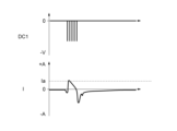
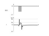
- a sudden current (hereinafter, this current is also referred to as a "transient current") may instantaneously flow through the upper electrode.
- the magnitude of the transient current tends to increase as the voltage level of the first DC signal (bias signal) increases.
- the transient current is considered to be a current necessary for stabilizing the plasma in the chamber, and if the transient current is limited by the circuit configuration of the power supply 30, etc., the plasma may become unstable. If the plasma becomes unstable, for example, an abnormal discharge may occur in the upper electrode (for example, the gas inlet 13c of the shower head 13, etc.).
- a plasma stabilization circuit described below such destabilization of the plasma may be suppressed.
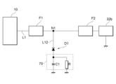
- FIG. 5 is a diagram showing a configuration example of a plasma stabilization circuit according to the first embodiment.
- the first embodiment is a configuration example in which a negative first DC signal is supplied to the lower electrode.
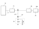
- a node N1 is provided on the transmission line L1 between the chamber 10 (upper electrode) and the second DC generating unit 32b.
- a first rectifying element D1 and a plasma stabilization circuit 70 are provided on the transmission line L12 between the node N1 and the ground potential.
- a first filter F1 and a second filter F2 are also provided on the transmission line L1 from the chamber 10 (upper electrode) toward the second DC generating unit 32b.
- the node N1 is on the transmission line L1 between the first filter F1 and the second filter F2.
- the first rectifying element D1 is provided on the transmission line L12 between the node N1 and the plasma stabilization circuit 70.
- the first rectifying element D1 may be provided in the transmission line L12 between the plasma stabilization circuit 70 and the ground potential.
- the second DC generating unit 32b generates a second DC signal of negative polarity.
- the second DC signal generated by the second DC generating unit 32b may have a slow pulse as shown in FIG. 4C.
- the second DC signal generated by the second DC generating unit 32b may have a constant voltage level as shown in FIG. 4D.
- the second waveform generating unit may not be provided.
- the second DC generating unit 32b may generate a second DC signal of positive polarity.
- the plasma stabilization circuit 70 includes a capacitor C1.
- the capacitance of the capacitor C1 is large enough to instantly supply a sufficient charge to the upper electrode.
- the capacitance of the capacitor C1 is 10 nF to 100 nF.
- the capacitor C1 may be composed of one or more capacitors.
- the plasma stabilization circuit 70 may be configured to include a resistor R as a static elimination circuit.
- the resistor R is connected in parallel to the capacitor C1.
- the resistor R may be configured to eliminate the charge in the capacitor C1 in about 1 to 10 seconds.
- an inductor may be used as the static elimination circuit instead of or in addition to the resistor R.
- the resistor R may be connected to a node on the transmission line L12 between the capacitor C1 and the first rectification element D1.
- the plasma stabilization circuit 70 instantaneously supplies the required amount of charge to the upper electrode, such as immediately after the first DC signal (bias signal) is supplied to the lower electrode. In other words, the plasma stabilization circuit 70 can prevent the plasma from becoming unstable by allowing a sufficient transient current to flow through the upper electrode.
- the first rectifier element D1 is positioned so that the chamber 10 (upper electrode) side is the forward direction of the current when viewed from the plasma stabilization circuit 70.
- the first rectifying element D1 may be configured as a diode.
- the cathode electrode of the first rectifying element D1 (diode) may be electrically connected to the node N1.
- the anode electrode of the first rectifying element D1 (diode) may be electrically connected to the plasma stabilization circuit 70. That is, the anode electrode of the first rectifying element D1 may be electrically connected to the ground potential via the capacitor C1 of the plasma stabilization circuit 70.
- the diode may be a mesa type or planar type PN junction diode.
- the first rectifying element D1 may be configured as a plurality of diodes, in which case the diodes may be connected directly or in parallel to each other.
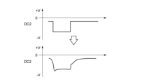
- the rectifying action of the first rectifying element D1 prevents the second DC signal from the second DC generating unit 32b from flowing to the plasma stabilization circuit 70. This prevents the voltage waveform of the second DC signal from being distorted by the large-capacity capacitor C1 of the plasma stabilization circuit 70.
- the first filter F1 is configured to filter signals (hereinafter referred to as "high frequency signals") in the frequency band of the source RF signal generated by the first RF generating unit 31a. That is, the first filter F1 blocks or attenuates the high frequency signal flowing from the chamber 10 (upper electrode) to the first rectifying element D1. This can prevent all or part of the high frequency signal from passing through the first rectifying element D1 to heat the first rectifying element D1, and thus prevent the rectifying action of the first rectifying element D1 from being reduced. It can also prevent the high frequency signal from entering the second DC generating unit 32b.
- the attenuation performance of the first filter F1 may be affected if the impedance of the first rectifying element D1 changes.
- the first rectifying element D1 is disposed on the output side (second DC generating unit 32b side) of the first filter F1. Therefore, the attenuation performance of the first filter F1 can be prevented from being affected by changes in the impedance of the first rectifying element D1.
- FIG. 6A is a diagram showing an example of the first filter F1.
- the first filter F1 may be configured to include one or more inductors (ID) and capacitors (C).
- the capacitance of the capacitor of the first filter F1 is sufficiently smaller than the capacitor C1 of the plasma stabilization circuit 70, and in one example, is 0.01 nF to 1 nF.
- the second filter F2 is configured to filter a signal (hereinafter referred to as a "bias pulse signal") in the pulse frequency band of the first DC signal (bias signal) generated by the first DC generating unit 32a. That is, the second filter F2 blocks or attenuates the bias pulse signal flowing from the first rectifying element D1 toward the second DC generating unit 32b. This can prevent the bias pulse signal from entering the second DC generating unit 32b. Note that if the second filter F2 causes interference with the second DC signal, the second filter F2 does not need to be provided. For example, if the second DC signal has a frequency close to the pulse frequency of the first DC signal (for example, within ⁇ 10%), the second filter F2 does not need to be provided.
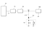
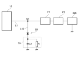
- FIGS. 7A and 7B are diagrams showing other arrangement examples of node N1.
- node N1 may be located on transmission line L1 between second filter F2 and second DC generating unit 32b.
- node N1 may be located on transmission line L1 between chamber 10 (upper electrode) and first filter F1.
- first filter F1 and second filter F2 may be integrated into one filter circuit.
- the node N1 may be between the first filter F1 and the second filter F2 (see FIG. 5). In this case, the node N1 may be between the second filter F2 and the second DC generating unit 32b (see FIG. 7A). This is because the current from the plasma stabilization circuit 70 to the upper electrode is less likely to be obstructed even if the first filter F1 or the second filter F2 is present.
- Second Embodiment 10 is a diagram showing a configuration example of a plasma stabilization circuit according to a second embodiment.
- the second embodiment is a configuration example in which a first DC signal of negative polarity is supplied to the lower electrode.
- a first filter provided in a transmission line between the upper electrode and the node, the first filter being configured to filter signals in an RF frequency band of the RF signal; 10.
- a chamber a substrate support disposed within the chamber and including at least one lower electrode; an upper electrode disposed above the substrate support; an RF signal generator electrically connected to any one of the at least one lower electrode or the upper electrode and configured to generate an RF signal to generate a plasma in the chamber; a voltage signal generator electrically connected to any one of the at least one lower electrode and configured to generate a voltage signal, the voltage signal having a sequence of voltage pulses; an impedance fixing circuit electrically connected to the upper electrode; A capacitor; a rectifying element including a first electrode and a second electrode, the first electrode being electrically connected to a node between the upper electrode and the impedance fixing circuit, and the second electrode being electrically connected to a ground potential via the capacitor;
- a plasma processing apparatus comprising:
- a chamber ; a substrate support disposed within the chamber and including an electrode; a first voltage signal generator electrically connected to the electrodes and configured to generate a first voltage signal, the first voltage signal having a sequence of first voltage pulses; an electrically conductive member that forms part of the chamber or is disposed within the chamber; A capacitor; a rectifying element including a first electrode and a second electrode, the first electrode being electrically connected to the conductive member and the second electrode being electrically connected to a ground potential via the capacitor;
- a plasma processing apparatus comprising:
- the conductive member is (a) an upper electrode disposed above the substrate support; (b) a ring assembly disposed on the substrate support to surround a substrate on the substrate support; (c) a liner disposed along an interior wall of the chamber; and (d) The plasma processing apparatus according to any one of claims 15 to 18, wherein the plasma processing apparatus is a baffle plate arranged to surround the substrate support.
- Plasma processing apparatus 1: Plasma processing apparatus, 2: Control unit, 10: Plasma processing chamber, 13: shower head, 31a: First RF generating unit, 31b: Second RF generating unit, 32a: First DC generating unit, 32b: Second DC generating unit, 50: Second waveform generating unit, 60: Impedance fixing circuit, 70: Plasma stabilization circuit, 80: Polarity switching circuit, D1: First rectifying element, D2: Second rectifying element, F1: First filter, F2: Second filter, L1: Transmission line
Landscapes
- Physics & Mathematics (AREA)
- Engineering & Computer Science (AREA)
- Plasma & Fusion (AREA)
- Chemical & Material Sciences (AREA)
- Analytical Chemistry (AREA)
- Electromagnetism (AREA)
- Spectroscopy & Molecular Physics (AREA)
- Plasma Technology (AREA)
- Chemical Vapour Deposition (AREA)
Abstract
Description
図1は、プラズマ処理システムの構成例を説明するための図である。一実施形態において、プラズマ処理システムは、プラズマ処理装置1及び制御部2を含む。プラズマ処理システムは、基板処理システムの一例であり、プラズマ処理装置1は、基板処理装置の一例である。プラズマ処理装置1は、プラズマ処理チャンバ10、基板支持部11及びプラズマ生成部12を含む。プラズマ処理チャンバ10は、プラズマ処理空間を有する。また、プラズマ処理チャンバ10は、少なくとも1つの処理ガスをプラズマ処理空間に供給するための少なくとも1つのガス供給口と、プラズマ処理空間からガスを排出するための少なくとも1つのガス排出口とを有する。ガス供給口は、後述するガス供給部20に接続され、ガス排出口は、後述する排気システム40に接続される。基板支持部11は、プラズマ処理空間内に配置され、基板を支持するための基板支持面を有する。
図3は、プラズマ処理装置1の電源30とプラズマ処理チャンバ10(以下「チャンバ10」ともいう。)との結合例を示す図である。
図4A~図4Dは、第1のDC信号及び第2のDC信号の電圧波形の一例を示すタイミングチャートである。一実施形態において、第1のDC信号及び第2のDC信号の電圧波形は、繰り返し期間Tで複数回繰り返されてよい(図4A~図4D参照)。一例では、第1のDC信号は、0.1kHz~50kHzの繰り返し周波数(1/T)を有してよい。一例では、第2のDC信号は、0.1kHz~50kHzの繰り返し周波数(1/T)を有してよい。第1のDC信号の繰り返し周波数と第2のDC信号の繰り返し周波数とは、同一であってよく、また異なっていてもよい。第1のDC信号と第2のDC信号とは同期してよく(図4A~図4C参照)、また同期しなくてもよい。例えば、第1のDC信号と第2のDC信号とは、所与の値(一例では180度)位相がずれていてもよい。
下部電極に第1のDC信号が供給された直後(例えば、高速パルスの1~3周期程度)において、上部電極に瞬間的に急激な電流(以下この電流を「過渡電流」ともいう)が流れる場合がある。過渡電流の大きさは、第1のDC信号(バイアス信号)の電圧レベルが大きくなると大きくなる傾向がある。過渡電流は、チャンバ内のプラズマの安定化に必要な電流と考えられ、電源30の回路構成等により、過渡電流が制限されると、プラズマが不安定化し得る。プラズマが不安定化すると、例えば、上部電極(例えば、シャワーヘッド13のガス導入口13c等)において異常放電等が生じ得る。第1の実施形態においては、以下に説明するプラズマ安定化回路を備えることにより、このようなプラズマの不安定化を抑制し得る。
図10は、第2の実施形態にかかるプラズマ安定化回路の構成例を示す図である。第2の実施形態は、下部電極に負極性の第1のDC信号が供給される場合の構成例である。以下、第1の実施形態と異なる構成を中心に説明する。
下部電極への第1のDC信号(バイアス信号)の供給によって上部電極に生じる電圧(以下「VDC電圧」ともいう。)に起因して、第2のDC信号によるプラズマの制御が不安定になる場合がある。例えば、上部電極におけるVDC電圧の電圧レベルが第2のDC信号の電圧レベルよりも大きくなると、上部電極に第2のDC信号と逆極性の電流が流れる(すなわち電流が逆流する)期間が生じる場合がある。電流が逆流している間は、第2のDC信号によるプラズマの制御ができず、チャンバ10内のプラズマが不安定化し得る。このような現象を抑制するために、一実施形態において、伝送ラインL1に第2の整流素子が設けられてよい。
図13は、プラズマ処理装置1の電源30とチャンバ10との他の結合例を示す図である。図13に示す例では、上部電極には、第2のDC生成部32bに代えて、インピーダンス固定回路60が伝送ラインL4を介して接続される。
図15Aは、第1の実施形態(図5)の変形例を示す図である。図15Bは、第2の実施形態(図10)の変形例を示す図である。これらの例は、第1のDC生成部32aで生成される第1のDC信号が正極性の場合の構成例である。なお、第2のDC生成部32bで生成される第2のDC信号は、正極性であってよく、また負極性であってもよい。
チャンバと、
前記チャンバ内に配置され、少なくとも1つの下部電極を含む基板支持部と、
前記基板支持部の上方に配置される上部電極と、
前記少なくとも1つの下部電極のいずれか又は前記上部電極に電気的に接続され、前記チャンバ内でプラズマを生成するためにRF信号を生成するように構成されるRF信号生成器と、
前記少なくとも1つの下部電極のいずれかに電気的に接続され、第1の電圧信号を生成するように構成される第1の電圧信号生成器であって、前記第1の電圧信号は、第1の電圧パルスのシーケンスを有する、第1の電圧信号生成器と、
前記上部電極に電気的に接続され、第2の電圧信号を生成するように構成される第2の電圧信号生成器と、
キャパシタと、
第1の電極及び第2の電極を含む整流素子であって、前記第1の電極は前記上部電極と前記第2の電圧信号生成器との間にあるノードに電気的に接続され、前記第2の電極は、前記キャパシタを介して接地電位に電気的に接続される、整流素子と、
を備える、プラズマ処理装置。
前記第2の電圧信号は、第2の電圧パルスのシーケンスを有する、付記1に記載のプラズマ処理装置。
前記第2の電圧信号は、一定の電圧レベルを有する、付記1に記載のプラズマ処理装置。
前記第2の電圧信号は、負極性を有し、前記第1の電極はカソード電極であり、前記第2の電極はアノード電極である、付記2に記載のプラズマ処理装置。
前記第1の電圧パルスのシーケンスは、0.1MHz~2MHzの範囲内にある第1のパルス周波数を有する、付記4に記載のプラズマ処理装置。
前記第2の電圧パルスのシーケンスは、0.1kHz~50kHzの範囲内にある第2のパルス周波数を有する、付記4又は付記5に記載のプラズマ処理装置。
前記上部電極と前記第2の電圧信号生成器との間の伝送ラインに設けられるフィルタ回路をさらに備える、付記1乃至付記6のいずれか1つに記載のプラズマ処理装置。
前記上部電極と前記ノードとの間の伝送ラインに設けられるフィルタ回路をさらに備える、付記1乃至付記7のいずれか1つに記載のプラズマ処理装置。
前記ノードと前記第2の電圧信号生成器との間の伝送ラインに設けられるフィルタ回路をさらに備える、付記1乃至付記8のいずれか1つに記載のプラズマ処理装置。
前記上部電極と前記ノードとの間の伝送ラインに設けられ、前記RF信号のRF周波数の帯域の信号をフィルタリングするように構成される第1のフィルタと、
前記ノードと前記第2の電圧信号生成器との間の伝送ラインに設けられ、前記第1の電圧パルスのシーケンスのパルス周波数の帯域の信号をフィルタリングするように構成される第2のフィルタと、をさらに備える、付記1乃至付記9のいずれか1つに記載のプラズマ処理装置。
チャンバと、
前記チャンバ内に配置され、少なくとも1つの下部電極を含む基板支持部と、
前記基板支持部の上方に配置される上部電極と、
前記少なくとも1つの下部電極のいずれか又は前記上部電極に電気的に接続され、前記チャンバ内でプラズマを生成するためにRF信号を生成するように構成されるRF信号生成器と、
前記少なくとも1つの下部電極のいずれかに電気的に接続され、電圧信号を生成するように構成される電圧信号生成器であって、前記電圧信号は、電圧パルスのシーケンスを有する、電圧信号生成器と、
前記上部電極に電気的に接続されるインピーダンス固定回路と、
キャパシタと、
第1の電極及び第2の電極を含む整流素子であって、前記第1の電極は前記上部電極と前記インピーダンス固定回路との間にあるノードに電気的に接続され、前記第2の電極は、前記キャパシタを介して接地電位に電気的に接続される、整流素子と、
を備える、プラズマ処理装置。
前記電圧パルスは、負極性を有し、前記第1の電極はカソード電極であり、前記第2の電極はアノード電極である、付記11に記載のプラズマ処理装置。
前記電圧パルスのシーケンスは、0.1MHz~2MHzの範囲内にある第1のパルス周波数を有する、付記11又は付記12に記載のプラズマ処理装置。
前記インピーダンス固定回路は、キャパシタ及びインダクタの少なくともいずれかを含む、付記11乃至付記13のいずれか1つに記載のプラズマ処理装置。
チャンバと、
前記チャンバ内に配置され、電極を含む基板支持部と、
前記電極に電気的に接続され、第1の電圧信号を生成するように構成される第1の電圧信号生成器であって、前記第1の電圧信号は、第1の電圧パルスのシーケンスを有する、第1の電圧信号生成器と、
前記チャンバの一部を構成する、又は、前記チャンバ内に配置される、導電性部材と、
キャパシタと、
第1の電極及び第2の電極を含む整流素子であって、前記第1の電極は前記導電性部材に電気的に接続され、前記第2の電極は、前記キャパシタを介して接地電位に電気的に接続される、整流素子と、
を備える、プラズマ処理装置。
前記導電性部材と前記整流素子の前記第1の電極との間にあるノードに電気的に接続され、第2の電圧信号を生成するように構成される第2の電圧信号生成器をさらに備える、付記15に記載のプラズマ処理装置。
前記導電性部材と前記整流素子の前記第1の電極との間にあるノードに電気的に接続されるインピーダンス固定回路をさらに備える、付記15に記載のプラズマ処理装置。
前記インピーダンス固定回路は、キャパシタ及びインダクタの少なくともいずれかを含む、付記17に記載のプラズマ処理装置。
前記導電性部材は、
(a)前記基板支持部の上方に配置される上部電極、
(b)前記基板支持部上の基板を囲むように前記基板支持部上に配置されるリングアセンブリ、
(c)前記チャンバの内壁に沿って配置されるライナ、及び、
(d)前記基板支持部を囲むように配置されるバッフルプレートのいずれかである、付記15乃至付記18のいずれか1つに記載のプラズマ処理装置。
Claims (19)
- チャンバと、
前記チャンバ内に配置され、少なくとも1つの下部電極を含む基板支持部と、
前記基板支持部の上方に配置される上部電極と、
前記少なくとも1つの下部電極のいずれか又は前記上部電極に電気的に接続され、前記チャンバ内でプラズマを生成するためにRF信号を生成するように構成されるRF信号生成器と、
前記少なくとも1つの下部電極のいずれかに電気的に接続され、第1の電圧信号を生成するように構成される第1の電圧信号生成器であって、前記第1の電圧信号は、第1の電圧パルスのシーケンスを有する、第1の電圧信号生成器と、
前記上部電極に電気的に接続され、第2の電圧信号を生成するように構成される第2の電圧信号生成器と、
キャパシタと、
第1の電極及び第2の電極を含む整流素子であって、前記第1の電極は前記上部電極と前記第2の電圧信号生成器との間にあるノードに電気的に接続され、前記第2の電極は、前記キャパシタを介して接地電位に電気的に接続される、整流素子と、
を備える、プラズマ処理装置。 - 前記第2の電圧信号は、第2の電圧パルスのシーケンスを有する、請求項1に記載のプラズマ処理装置。
- 前記第2の電圧信号は、一定の電圧レベルを有する、請求項1に記載のプラズマ処理装置。
- 前記第2の電圧信号は、負極性を有し、前記第1の電極はカソード電極であり、前記第2の電極はアノード電極である、請求項2に記載のプラズマ処理装置。
- 前記第1の電圧パルスのシーケンスは、0.1MHz~2MHzの範囲内にある第1のパルス周波数を有する、請求項4に記載のプラズマ処理装置。
- 前記第2の電圧パルスのシーケンスは、0.1kHz~50kHzの範囲内にある第2のパルス周波数を有する、請求項5に記載のプラズマ処理装置。
- 前記上部電極と前記第2の電圧信号生成器との間の伝送ラインに設けられるフィルタ回路をさらに備える、請求項1に記載のプラズマ処理装置。
- 前記上部電極と前記ノードとの間の伝送ラインに設けられるフィルタ回路をさらに備える、請求項1に記載のプラズマ処理装置。
- 前記ノードと前記第2の電圧信号生成器との間の伝送ラインに設けられるフィルタ回路をさらに備える、請求項1に記載のプラズマ処理装置。
- 前記上部電極と前記ノードとの間の伝送ラインに設けられ、前記RF信号のRF周波数の帯域の信号をフィルタリングするように構成される第1のフィルタと、
前記ノードと前記第2の電圧信号生成器との間の伝送ラインに設けられ、前記第1の電圧パルスのシーケンスのパルス周波数の帯域の信号をフィルタリングするように構成される第2のフィルタと、をさらに備える、請求項1に記載のプラズマ処理装置。 - チャンバと、
前記チャンバ内に配置され、少なくとも1つの下部電極を含む基板支持部と、
前記基板支持部の上方に配置される上部電極と、
前記少なくとも1つの下部電極のいずれか又は前記上部電極に電気的に接続され、前記チャンバ内でプラズマを生成するためにRF信号を生成するように構成されるRF信号生成器と、
前記少なくとも1つの下部電極のいずれかに電気的に接続され、電圧信号を生成するように構成される電圧信号生成器であって、前記電圧信号は、電圧パルスのシーケンスを有する、電圧信号生成器と、
前記上部電極に電気的に接続されるインピーダンス固定回路と、
キャパシタと、
第1の電極及び第2の電極を含む整流素子であって、前記第1の電極は前記上部電極と前記インピーダンス固定回路との間にあるノードに電気的に接続され、前記第2の電極は、前記キャパシタを介して接地電位に電気的に接続される、整流素子と、
を備える、プラズマ処理装置。 - 前記電圧パルスは、負極性を有し、前記第1の電極はカソード電極であり、前記第2の電極はアノード電極である、請求項11に記載のプラズマ処理装置。
- 前記電圧パルスのシーケンスは、0.1MHz~2MHzの範囲内にある第1のパルス周波数を有する、請求項12に記載のプラズマ処理装置。
- 前記インピーダンス固定回路は、キャパシタ及びインダクタの少なくともいずれかを含む、請求項13に記載のプラズマ処理装置。
- チャンバと、
前記チャンバ内に配置され、電極を含む基板支持部と、
前記電極に電気的に接続され、第1の電圧信号を生成するように構成される第1の電圧信号生成器であって、前記第1の電圧信号は、第1の電圧パルスのシーケンスを有する、第1の電圧信号生成器と、
前記チャンバの一部を構成する、又は、前記チャンバ内に配置される、導電性部材と、
キャパシタと、
第1の電極及び第2の電極を含む整流素子であって、前記第1の電極は前記導電性部材に電気的に接続され、前記第2の電極は、前記キャパシタを介して接地電位に電気的に接続される、整流素子と、
を備える、プラズマ処理装置。 - 前記導電性部材と前記整流素子の前記第1の電極との間にあるノードに電気的に接続され、第2の電圧信号を生成するように構成される第2の電圧信号生成器をさらに備える、請求項15に記載のプラズマ処理装置。
- 前記導電性部材と前記整流素子の前記第1の電極との間にあるノードに電気的に接続されるインピーダンス固定回路をさらに備える、請求項15に記載のプラズマ処理装置。
- 前記インピーダンス固定回路は、キャパシタ及びインダクタの少なくともいずれかを含む、請求項17に記載のプラズマ処理装置。
- 前記導電性部材は、
(a)前記基板支持部の上方に配置される上部電極、
(b)前記基板支持部上の基板を囲むように前記基板支持部上に配置されるリングアセンブリ、
(c)前記チャンバの内壁に沿って配置されるライナ、及び、
(d)前記基板支持部を囲むように配置されるバッフルプレートのいずれかである、請求項15乃至請求項18のいずれか一項に記載のプラズマ処理装置。
Priority Applications (4)
| Application Number | Priority Date | Filing Date | Title |
|---|---|---|---|
| CN202480059207.8A CN121890253A (zh) | 2023-09-29 | 2024-07-16 | 等离子体处理装置 |
| KR1020267012620A KR20260087611A (ko) | 2023-09-29 | 2024-07-16 | 플라즈마 처리 장치 |
| JP2025548527A JPWO2025069652A1 (ja) | 2023-09-29 | 2024-07-16 | |
| US19/571,522 US20260213131A1 (en) | 2023-09-29 | 2026-03-19 | Plasma processing apparatus |
Applications Claiming Priority (2)
| Application Number | Priority Date | Filing Date | Title |
|---|---|---|---|
| JP2023169603 | 2023-09-29 | ||
| JP2023-169603 | 2023-09-29 |
Related Child Applications (1)
| Application Number | Title | Priority Date | Filing Date |
|---|---|---|---|
| US19/571,522 Continuation US20260213131A1 (en) | 2023-09-29 | 2026-03-19 | Plasma processing apparatus |
Publications (1)
| Publication Number | Publication Date |
|---|---|
| WO2025069652A1 true WO2025069652A1 (ja) | 2025-04-03 |
Family
ID=95202879
Family Applications (1)
| Application Number | Title | Priority Date | Filing Date |
|---|---|---|---|
| PCT/JP2024/025501 Ceased WO2025069652A1 (ja) | 2023-09-29 | 2024-07-16 | プラズマ処理装置 |
Country Status (6)
| Country | Link |
|---|---|
| US (1) | US20260213131A1 (ja) |
| JP (1) | JPWO2025069652A1 (ja) |
| KR (1) | KR20260087611A (ja) |
| CN (1) | CN121890253A (ja) |
| TW (1) | TW202531300A (ja) |
| WO (1) | WO2025069652A1 (ja) |
Citations (3)
| Publication number | Priority date | Publication date | Assignee | Title |
|---|---|---|---|---|
| JP2022018062A (ja) * | 2020-07-14 | 2022-01-26 | 東京エレクトロン株式会社 | プラズマ処理装置およびプラズマ処理方法 |
| JP2022080674A (ja) * | 2020-11-18 | 2022-05-30 | 東京エレクトロン株式会社 | プラズマ処理装置 |
| JP2023013666A (ja) * | 2021-07-16 | 2023-01-26 | 東京エレクトロン株式会社 | プラズマ処理装置及び処理方法 |
Family Cites Families (2)
| Publication number | Priority date | Publication date | Assignee | Title |
|---|---|---|---|---|
| KR101248691B1 (ko) | 2004-06-21 | 2013-04-03 | 도쿄엘렉트론가부시키가이샤 | 플라즈마 처리 장치 |
| US11848176B2 (en) | 2020-07-31 | 2023-12-19 | Applied Materials, Inc. | Plasma processing using pulsed-voltage and radio-frequency power |
-
2024
- 2024-07-16 KR KR1020267012620A patent/KR20260087611A/ko active Pending
- 2024-07-16 CN CN202480059207.8A patent/CN121890253A/zh active Pending
- 2024-07-16 JP JP2025548527A patent/JPWO2025069652A1/ja active Pending
- 2024-07-16 WO PCT/JP2024/025501 patent/WO2025069652A1/ja not_active Ceased
- 2024-08-22 TW TW113131546A patent/TW202531300A/zh unknown
-
2026
- 2026-03-19 US US19/571,522 patent/US20260213131A1/en active Pending
Patent Citations (3)
| Publication number | Priority date | Publication date | Assignee | Title |
|---|---|---|---|---|
| JP2022018062A (ja) * | 2020-07-14 | 2022-01-26 | 東京エレクトロン株式会社 | プラズマ処理装置およびプラズマ処理方法 |
| JP2022080674A (ja) * | 2020-11-18 | 2022-05-30 | 東京エレクトロン株式会社 | プラズマ処理装置 |
| JP2023013666A (ja) * | 2021-07-16 | 2023-01-26 | 東京エレクトロン株式会社 | プラズマ処理装置及び処理方法 |
Also Published As
| Publication number | Publication date |
|---|---|
| TW202531300A (zh) | 2025-08-01 |
| US20260213131A1 (en) | 2026-07-23 |
| KR20260087611A (ko) | 2026-06-11 |
| CN121890253A (zh) | 2026-04-17 |
| JPWO2025069652A1 (ja) | 2025-04-03 |
Similar Documents
| Publication | Publication Date | Title |
|---|---|---|
| JP7828799B2 (ja) | プラズマ処理装置及びプラズマ処理方法 | |
| JP7860120B2 (ja) | プラズマ処理システム及びプラズマ処理方法 | |
| KR20240012306A (ko) | 플라즈마 처리 장치 | |
| KR20220170370A (ko) | 플라즈마 처리 방법 및 플라즈마 처리 장치 | |
| US20250357088A1 (en) | Plasma processing apparatus | |
| JP7765772B1 (ja) | プラズマ処理装置及び基板支持器 | |
| JP2025114638A (ja) | プラズマ処理装置及びプラズマ処理方法 | |
| WO2025069651A1 (ja) | プラズマ処理装置 | |
| WO2025047033A1 (ja) | プラズマ処理装置及びインピーダンス整合方法 | |
| TW202531300A (zh) | 電漿處理裝置 | |
| WO2025169740A1 (ja) | プラズマ処理装置、電源システム、制御方法、及びプログラム | |
| WO2026048593A1 (ja) | プラズマ処理装置及びrf生成器 | |
| US20260088250A1 (en) | Plasma processing apparatus | |
| WO2025053086A1 (ja) | プラズマ処理装置及びプラズマ処理方法 | |
| WO2026100357A1 (ja) | プラズマ処理装置 | |
| TW202529152A (zh) | 電漿處理裝置及電源單元 | |
| WO2025089081A1 (ja) | プラズマ処理装置 | |
| WO2026034233A1 (ja) | プラズマ処理装置及び電源システム | |
| JP2026004103A (ja) | プラズマ処理装置及びプラズマ処理方法 | |
| WO2026034234A1 (ja) | プラズマ処理装置及び電源システム | |
| JP2025064037A (ja) | 静電チャック、基板支持器、及びプラズマ処理装置 | |
| JP2024098586A (ja) | プラズマ処理装置及び制御方法 | |
| WO2025164456A1 (ja) | プラズマ処理装置 | |
| WO2025089271A1 (ja) | 基板支持器及びプラズマ処理装置 | |
| TW202448216A (zh) | 電漿處理裝置及電漿處理方法 |
Legal Events
| Date | Code | Title | Description |
|---|---|---|---|
| 121 | Ep: the epo has been informed by wipo that ep was designated in this application |
Ref document number: 24871456 Country of ref document: EP Kind code of ref document: A1 |
|
| ENP | Entry into the national phase |
Ref document number: 2025548527 Country of ref document: JP Kind code of ref document: A |
|
| WWE | Wipo information: entry into national phase |
Ref document number: 2025548527 Country of ref document: JP |
|
| NENP | Non-entry into the national phase |
Ref country code: DE |
|
| WWE | Wipo information: entry into national phase |
Ref document number: 11202601678W Country of ref document: SG |
|
| WWP | Wipo information: published in national office |
Ref document number: 11202601678W Country of ref document: SG |