WO2025063035A1 - 炭化珪素単結晶の製造方法および炭化珪素単結晶の製造装置 - Google Patents
炭化珪素単結晶の製造方法および炭化珪素単結晶の製造装置 Download PDFInfo
- Publication number
- WO2025063035A1 WO2025063035A1 PCT/JP2024/031477 JP2024031477W WO2025063035A1 WO 2025063035 A1 WO2025063035 A1 WO 2025063035A1 JP 2024031477 W JP2024031477 W JP 2024031477W WO 2025063035 A1 WO2025063035 A1 WO 2025063035A1
- Authority
- WO
- WIPO (PCT)
- Prior art keywords
- silicon carbide
- crucible
- covering member
- single crystal
- seed crystal
- Prior art date
- Legal status (The legal status is an assumption and is not a legal conclusion. Google has not performed a legal analysis and makes no representation as to the accuracy of the status listed.)
- Pending
Links
Images


Classifications
-
- C—CHEMISTRY; METALLURGY
- C30—CRYSTAL GROWTH
- C30B—SINGLE-CRYSTAL GROWTH; UNIDIRECTIONAL SOLIDIFICATION OF EUTECTIC MATERIAL OR UNIDIRECTIONAL DEMIXING OF EUTECTOID MATERIAL; REFINING BY ZONE-MELTING OF MATERIAL; PRODUCTION OF A HOMOGENEOUS POLYCRYSTALLINE MATERIAL WITH DEFINED STRUCTURE; SINGLE CRYSTALS OR HOMOGENEOUS POLYCRYSTALLINE MATERIAL WITH DEFINED STRUCTURE; AFTER-TREATMENT OF SINGLE CRYSTALS OR A HOMOGENEOUS POLYCRYSTALLINE MATERIAL WITH DEFINED STRUCTURE; APPARATUS THEREFOR
- C30B23/00—Single-crystal growth by condensing evaporated or sublimed materials
-
- C—CHEMISTRY; METALLURGY
- C30—CRYSTAL GROWTH
- C30B—SINGLE-CRYSTAL GROWTH; UNIDIRECTIONAL SOLIDIFICATION OF EUTECTIC MATERIAL OR UNIDIRECTIONAL DEMIXING OF EUTECTOID MATERIAL; REFINING BY ZONE-MELTING OF MATERIAL; PRODUCTION OF A HOMOGENEOUS POLYCRYSTALLINE MATERIAL WITH DEFINED STRUCTURE; SINGLE CRYSTALS OR HOMOGENEOUS POLYCRYSTALLINE MATERIAL WITH DEFINED STRUCTURE; AFTER-TREATMENT OF SINGLE CRYSTALS OR A HOMOGENEOUS POLYCRYSTALLINE MATERIAL WITH DEFINED STRUCTURE; APPARATUS THEREFOR
- C30B29/00—Single crystals or homogeneous polycrystalline material with defined structure characterised by the material or by their shape
- C30B29/10—Inorganic compounds or compositions
- C30B29/36—Carbides
Definitions
- This disclosure relates to a method for producing silicon carbide (hereinafter referred to as "SiC”) single crystals and an apparatus for producing SiC single crystals.
- SiC silicon carbide
- a method and apparatus for producing SiC single crystals in which a heating unit is placed around the periphery of a graphite crucible is known, for example, as a sublimation recrystallization method.
- a seed crystal is placed at the top of the graphite crucible, and SiC powder raw material placed at the bottom of the crucible is heated to, for example, 2300°C, thereby sublimating the SiC powder raw material, and the sublimated gas is recrystallized on the seed crystal, which is set at a temperature lower than the raw material temperature.
- Patent Document 1 has proposed this type of SiC single crystal production method and production apparatus.
- the SiC single crystal manufacturing apparatus described in Patent Document 1 has a skirt portion in the shape of a truncated cone that expands in a tapered shape around a seed crystal, and the entire surface of the skirt portion is covered with a TaC member made of tantalum carbide (TaC).
- TaC member made of tantalum carbide (TaC).
- This TaC member is formed into a cup shape along the inner wall surface of the skirt portion by deep drawing a plate-shaped TaC, and has a seamless shape, which prevents the graphite on the inner wall surface of the skirt portion from being exposed.
- the SiC single crystal manufacturing apparatus described above can suppress the deterioration of the crystal quality of the SiC single crystal caused by carbon originating from the graphite in the skirt portion being taken into the SiC single crystal grown on the seed crystal, and the occurrence of defects caused by seams and cuts in the TaC member.
- this type of SiC single crystal manufacturing apparatus it has been newly discovered that if the entire area of the inner wall surface of the crucible in which the SiC powder raw material is placed is covered with a coating material having a higher melting point than SiC, such as TaC, the carbon atoms become insufficient and silicon becomes excessive, which in turn reduces the crystal quality of the SiC single crystal.
- the inventors of the present invention have considered locally exposing a part of the inner wall surface of the crucible that is far from the seed crystal, and it has become further clear that repeated production of SiC single crystals causes the part of the area to be worn out and a hole to be formed in the crucible. In this case, problems occur such as dust generated by the opening of a hole in the crucible being taken into the SiC single crystal, or gas obtained by sublimating the SiC powder raw material escaping from the hole to the outside of the crucible.
- This disclosure relates to a method and apparatus for producing SiC single crystals that can suppress the incorporation of carbon from the graphite in the crucible and the deterioration of the crystal quality of the SiC single crystals that results from localized wear of the crucible.
- a method for producing silicon carbide single crystals includes preparing a hollow cylindrical crucible having a bottomed cylindrical container body, a lid for closing an opening of the container body, and a covering member made of a metal carbide having a melting point higher than the growth temperature of silicon carbide and disposed inside the container body; disposing a seed crystal made of a silicon carbide substrate on the lid, disposing a silicon carbide raw material in the container body, and then supplying a sublimation gas of the silicon carbide raw material to grow a silicon carbide single crystal on the seed crystal; in preparing the crucible, the space in the crucible from the height position of the surface of the seed crystal to the height position of the surface of the silicon carbide raw material is defined as a growth space, the wall surface of the growth space is defined as a side surface, the covering member is tubular along the side surface, and a predetermined region of the side surface from the height position of the surface of the seed crystal is covered with the covering member.
- the method for producing a SiC single crystal comprises preparing a crucible having a container body, a lid body, and a covering member, placing a seed crystal on the lid body, placing a SiC raw material in the container body, and then sublimating the SiC raw material to grow a SiC single crystal on the seed crystal. Then, a cylindrical covering member made of a metal carbide having a melting point higher than the growth temperature of SiC is prepared, and a part of the side of the growth space, which is the space in the crucible from the surface position of the seed crystal to the surface position of the SiC raw material and is filled with the sublimation gas of the SiC raw material, is covered with the covering member.
- the area covered with the covering member is a predetermined part of the side from the surface position of the seed crystal toward the SiC raw material.
- This method for producing a SiC single crystal covers the graphite near the seed crystal surface on the side of the crucible with the covering member, so that carbon derived from the graphite can be suppressed from being incorporated into the SiC single crystal.
- this method for producing SiC single crystals exposes a sufficient area of graphite on the side surface away from the seed crystal surface, which can prevent localized wear and tear on the crucible and the formation of holes.
- a silicon carbide single crystal manufacturing apparatus includes a crucible having a bottomed cylindrical container body, a member to which a seed crystal made of a silicon carbide substrate is attached, a lid that closes the opening of the container body, and a covering member made of a metal carbide having a melting point higher than the growth temperature of silicon carbide, the portion of the crucible located on the surface of the silicon carbide raw material to be placed is defined as the raw material height position, the portion of the crucible located on the surface of the seed crystal to be placed is defined as the seed crystal height position, the space from the raw material height position to the seed crystal height position and filled with sublimation gas of the silicon carbide raw material is defined as the growth space, the wall surface of the crucible in the growth space is defined as the side surface, and the covering member is cylindrical along the side surface and covers a predetermined region of the side surface from the seed crystal height position toward the raw material height position.
- the SiC single crystal manufacturing apparatus is configured such that in the growth space of the crucible from the surface of the seed crystal to the surface of the SiC raw material, a certain region of the side surface exposed to the sublimation gas from the seed crystal surface is covered with a covering member made of a metal carbide having a higher melting point than SiC. Since the side surface of the crucible in the vicinity of the seed crystal surface is covered with graphite, the SiC single crystal manufacturing apparatus can suppress the incorporation of carbon derived from the graphite into the SiC single crystal.
- the SiC single crystal manufacturing apparatus can suppress localized wear of the crucible and the occurrence of holes while preventing the sublimation gas of the raw material from becoming excessively silicon.
- FIG. 1 is a diagram showing a cross-sectional configuration of a SiC single crystal manufacturing apparatus according to a first embodiment.
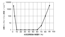
- FIG. 1 is a diagram showing the relationship between the coverage rate of the side surface by the covering member in the growth space and the carbon inclusion density in the SiC single crystal.
- FIG. 4 is a diagram showing a cross-sectional configuration of a SiC single crystal manufacturing apparatus according to a second embodiment.
- FIG. 10A to 10C are explanatory views of the carbonization treatment of the covering member that covers the skirt portion.
- FIG. 11 is a diagram showing a cross-sectional configuration of a SiC single crystal manufacturing apparatus according to a third embodiment.
- FIG. 13 is a diagram showing a modified example of the SiC single crystal manufacturing apparatus of the third embodiment.
- a seed crystal 40 and a raw material 50 placed in a crucible 1 described later, and a SiC single crystal 60 growing on the seed crystal 40 are shown. This also applies to Figs. 3, 6, and 7 described later.
- the SiC single crystal manufacturing apparatus includes a crucible 1 including a cylindrical container body 10 with a bottom, a circular lid body 20, and a covering member 30.
- the crucible 1 has, for example, a hollow cylindrical shape with the container body 10 and the lid body 20 made of graphite.
- the container body 10 has, for example, a SiC raw material 50, which is a supply source of sublimation gas, disposed at the bottom of the inner cylinder.
- the raw material 50 is, for example, powdered SiC crystal.
- the container body 10 has an opening on the lid 20 side at the top, and the wall surface on the side where the raw material 50 is disposed as the inner wall surface 10a, and a predetermined region from the upper side of the inner wall surface 10a is covered with a covering member 30.
- the container body 10 has a predetermined region of the inner wall surface 10a that is covered by the covering member 30 from the height position of the surface 40a of the seed crystal 40, and the inner wall surface 10a is exposed in other regions.
- Si-excessive sublimation gas such as Si and Si 2 C is generated, so if the entire side surface 12 described later is covered with the covering member 30, carbon in the SiC single crystal may be insufficient, and the crystal quality may be reduced. In addition, it is difficult to adjust the Si/C ratio in the powdered SiC crystal and suppress the generation of Si-excessive sublimation gas. For this reason, a part of the inner wall surface 10a of the container body 10 is left uncovered by the covering member 30, so that carbon atoms from the part of the graphite are used for recrystallization of SiC, and serve to suppress deterioration of crystal quality caused by Si-excessive sublimation gas.
- the entire lower region of the inner wall surface 10a on the source material 50 side from a position a predetermined distance away from the surface 40a of the seed crystal 40 is left as a region not covered by the covering member 30, and is made a large area, so that localized wear during the growth process of the SiC single crystal is suppressed.
- the position of the surface 40a of the seed crystal 40 in the crucible 1 will be referred to as the "height position 1A” and the position of the surface 50a of the raw material 50 will be referred to as the “height position 1B” as shown in FIG. 1.
- the height position here means the position in the height direction, for example, along the normal direction to the bottom surface 10b inside the crucible 1, connecting the bottom surface 10b and the opening closed by the lid 20.
- the lid 20 side in the height direction may be referred to as the upper side
- the bottom surface 10b side on the inside of the container body 10 may be referred to as the lower side.
- the space from the height position 1A to the height position 1B in the crucible 1, which is filled with the sublimation gas of the raw material 50, will be referred to as the "growth space 11", and the wall surface facing the growth space 11 will be referred to as the "side surface 12".
- the position of the surface 50a of the raw material 50 is the position of the flat surface when the surface 50a is arranged flat, for example, by tapping the crucible 1 after the raw material 50 is put into the container body 10. Also, when the surface 50a of the raw material 50 is not arranged flat, the position of the surface 50a is the average position in the height direction of the unevenness of the outermost surface of the seed crystal 40 side of the raw material 50, or the average position in the height direction of the part of the outermost surface that contacts the inner wall surface 10a. Since the seed crystal 40 has a thin thickness that can be ignored, the area below the height position of the surface of the lid 20 to which the seed crystal 40 is attached may be regarded as the growth space 11.
- the area of the container body 10 where the raw material 50 is arranged is regarded as the raw material arrangement area, and some kind of mark indicating the upper end of the raw material arrangement area is attached to the inner wall surface 10a, the area above the mark may be regarded as the growth space 11.
- the side surface 12 is part of the inner wall surface 10a of the container body 10, and is configured as a portion exposed to the sublimation gas of the raw material 50.
- the side surface 12 has a height dimension of, for example, about 30 mm to 500 mm, depending on the height from the bottom surface 10b of the raw material 50, i.e., the amount.
- the height dimension of the side surface 12 is the dimension of the growth space 11, and can be changed as appropriate depending on the size and thickness of the SiC single crystal 60 to be obtained.
- the lid body 20 is, for example, disk-shaped, and a SiC seed crystal 40 is attached to the surface that covers the opening of the container body 10.
- the seed crystal 40 is, for example, a SiC substrate, and is attached so that the surface 40a faces away from the lid body 20.
- the covering member 30 is made of a carbide with a melting point higher than the growth temperature of SiC, which will be described later, and covers a predetermined region of the inner wall surface 10a of the container body 10 from the height position 1A of the seed crystal 40.
- the covering member 30 is provided to prevent graphite from being exposed in the region of the inner wall surface 10a of the container body 10 near the seed crystal 40, and thus to prevent carbon particles from the graphite from being incorporated into the SiC single crystal 60 grown on the seed crystal 40, causing deterioration in the quality of the crystal.
- the end of the covering member 30 facing the seed crystal 40 may be referred to as the "upper end” and the end facing the raw material 50 as the “lower end”.
- the covering member 30 covers the entire area of the side surface 12 located from the upper end to the lower end of the covering member 30.
- the upper end of the covering member 30 coincides with, for example, height position 1A, i.e., the position of the surface 40a of the seed crystal 40.
- the covering member 30 is composed of, for example, any one of the carbides of tantalum, niobium, tungsten, and titanium.
- the covering member 30 is attached, for example, to a portion of the side surface 12 from height position 1A toward height position 1B, and is cylindrical along the side surface 12.
- the covering member 30 has a covering portion that is the portion of the side surface 12 that is covered by the covering member 30, and the ratio of the area of the covering portion to the entire area of the side surface 12 is the covering rate, which is set within a predetermined range described below.
- the carbon inclusion density which is the density of carbon particles mixed in the SiC single crystal 60
- the carbon inclusion density was 1 cm ⁇ 3 or less, and the crystal quality was good.
- the carbon inclusion density started to increase when the coverage was less than 10%, and reached about 100 cm ⁇ 3 at a coverage of 5%, and further increased dramatically to exceed 1000 cm ⁇ 3 when the coverage was less than 5%.
- the carbon inclusion density started to increase when the coverage exceeded 60%, and reached about 100 cm ⁇ 3 at a coverage of 80%, and further increased dramatically to exceed 1000 cm ⁇ 3 when the coverage exceeded 80%.
- This result shows that the crystal quality of the SiC single crystal 60 can be ensured well by setting the coverage within the range of 5% or more and 80% or less, more preferably 10% or more and 60% or less.
- the carbon inclusion density on the vertical axis of FIG. 2 was measured by growing SiC single crystal 60 up to the lowest height position on the raw material 50 side of the portion of side surface 12 covered with coating member 30, and then extracting a 1 mm thick substrate crystal from surface 60a of SiC single crystal 60.
- the carbon inclusion density in FIG. 2 was obtained by observing the 1 mm thick substrate crystal with an optical microscope and counting the number of carbon inclusions with a diameter of 1 ⁇ m or more observed in a specified area of the substrate crystal. Furthermore, according to the inventors' investigations, the carbon inclusion density of SiC single crystal 60 was found to be independent of the inner diameter or height dimension of side surface 12.
- the coating member 30 can be obtained, for example, by preparing a plate material having a thickness of 0.1 mm to 3 mm and made of the above-mentioned metal material, processing the plate material into a shape that conforms to the inner wall surface 10a of the container body 10, and then carbonizing the plate material.
- a graphite member having a shape that conforms to the inner wall surface 10a of the container body 10 is prepared, and the processed plate material is placed adjacent to the graphite member and then carbonized by performing a heat treatment at 1500°C to 2500°C in an inert atmosphere, for example an argon atmosphere.
- the above process can obtain a coating member 30 made of metal carbide.
- a coating member 30 without pinholes or cracks can be formed even when the diameter of the side surface 12 is, for example, 6 inches or more, and SiC single crystals 60 can be stably manufactured.
- the ratio of carbon to tantalum is defined as the C/Ta ratio, which is in the range of 0.2 to 1. This is based on the results of performing crystal growth on tantalum carbide coating members with C/Ta ratios of 0, 0.2, 0.4, 0.6, 0.8, and 1.0, and checking the deformation and damage of the coating member 30 due to crystal growth. Good crystal growth was possible when the C/Ta ratio was in the range of 0.2 to 1. On the other hand, when the C/Ta ratio is less than 0.2, the dimensional change during growth of the SiC single crystal 60 becomes too large, and partial silicidation occurs, resulting in a low melting point, which may cause damage to the coating member 30. This result was independent of the coverage rate of the coating member 30.
- the change rate of the dimensions and weight due to the carbonization treatment is 1% to 10% based on the dimensions and weight before the carbonization treatment.
- the C/Ta ratio is less than 0.2
- the change rate of the dimensions and weight of the covering member 30 during the SiC crystal growth process is large, exceeding 10%, and deformation and damage occurred.
- the C/Ta ratio is within the range of 0.2 to 1
- the dimensions and weight of the covering member 30 change in advance during the carbonization process, so that large deformation and damage of the covering member 30 during the SiC crystal growth process can be prevented.
- the dimensions of the covering member 30 before the carbonization treatment are determined, for example, taking into account the change rate of the dimensions and weight due to the carbonization treatment, so that the dimensions after the carbonization treatment are approximately the same as the inner diameter of the inner wall surface 10a.
- the C/Ta ratio in the tantalum carbide can be calculated, for example, by the following method.
- the tantalum member after carbonization is powdered, and the obtained powder is subjected to X-ray diffraction measurement.
- the peak heights derived from the crystal phases of NaCl structure TaC, trigonal Ta 3 C 2 , Ta 4 C 3 , hexagonal Ta 2 C, and body-centered cubic Ta are confirmed, and the ratio of each crystal phase is identified.
- the carbon ratio in each of the above structures is 1 for NaCl structure TaC, 0.67 to 0.75 for trigonal Ta 3 C 2 and Ta 4 C 3 , 0.5 for hexagonal Ta 2 C, and 0 for body-centered cubic Ta. Then, the C/Ta ratio in each growth phase is identified from the lattice constant of each crystal phase, and the C/Ta ratio in the tantalum carbide can be calculated from the overall ratio. For this reason, it is considered sufficient for the covering member 30 to have an average C/Ta ratio throughout the entire region within the range of 0.2 or more and 1 or less.
- the SiC single crystal manufacturing apparatus has a heating unit (not shown) arranged to surround the outer periphery of the crucible 1.
- a crucible 1 having a container body 10, a lid 20, and a covering member 30 is prepared, a seed crystal 40 is attached to the inner surface of the lid 20, and raw material 50 is placed on the bottom surface 10b of the container body 10.
- the seed crystal 40 is prepared to be, for example, a substantially circular plate with a diameter in the range of 150 mm to 220 mm.
- the crucible 1 is placed in a heating chamber (not shown) and heated by any heating unit such as a heater in a fixed position, and the crucible 1 is heated by the radiant heat to a predetermined temperature inside the crucible 1.
- the growth space 11 in the crucible 1 is made into an Ar atmosphere with a pressure of about 100 Pa to 10,000 Pa, the temperature of the raw material 50 is made to be about 2100°C to 2400°C, and the temperature of the seed crystal 40 is made to be about 2000°C to 2300°C, which is lower than that of the raw material 50.
- the atmosphere in the chamber is obtained by, for example, flowing in an inert gas such as Ar gas through an air supply pipe (not shown) while exhausting air through an exhaust pipe (not shown).
- an inert gas such as Ar gas
- the atmospheric pressure in the heating chamber is kept close to atmospheric pressure to suppress sublimation from the raw material 50, and once the target temperature is reached, the above-mentioned reduced pressure atmosphere is created.
- the raw material 50 sublimes and a sublimation gas is generated from the raw material 50.
- This sublimation gas is supplied to the surface 40a of the seed crystal 40.
- the sublimation gas crystallizes on the surface 40a of the seed crystal 40, and a SiC single crystal 60 grows.
- nitrogen gas is introduced as necessary to control the resistivity of the crystal.
- the crucible 1 has a side surface 12 of the growth space 11 covered with a covering member 30 made of a metal carbide with a melting point higher than the growth temperature of SiC.
- a predetermined region of the side surface 12 from the height position 1A of the seed crystal 40 is covered with the covering member 30 at a coverage rate of 5% to 80%, and graphite is exposed in the remaining part of the side surface 12.
- the graphite of the side surface 12 is not exposed near the seed crystal 40, and it is possible to prevent carbon resulting from the graphite from being mixed into the SiC single crystal 60.
- the graphite is exposed from the covering member 30 in the region of the side surface 12 far from the seed crystal 40, it is possible to prevent excess Si in the sublimation gas of the raw material 50 and to prevent partial consumption of the graphite of the side surface 12 in the growth process of the SiC single crystal 60.
- a SiC single crystal manufacturing apparatus and manufacturing method are provided that are capable of suppressing the incorporation of carbon derived from the graphite in the crucible 1 and the deterioration of the crystal quality of the SiC single crystal 60 caused by localized wear of the crucible 1.
- the carbon inclusion density in the SiC single crystal 60 becomes a predetermined value or less, and good crystal quality can be ensured.
- the ratio of the dimensions in the height direction between the raw material placement area and the remaining area is set to ⁇ : ⁇ ( ⁇ and ⁇ are any positive numbers).
- the covering member 30 may be placed so that the coverage rate of the wall surface of the area of the closed space from the end on the lid body 20 side downward to a ratio of ⁇ /( ⁇ + ⁇ ) is 5% to 80%, and more preferably 10% to 60%.
- the SiC single crystal 60 By growing the SiC single crystal 60 within the area covered by the covering member 30, carbon originating from exposed graphite on the side surface 12 is prevented from being incorporated into the SiC single crystal 60, making it possible to ensure good crystal quality.
- the height from the surface 40a of the seed crystal 40 to the surface 60a of the SiC single crystal 60 along the normal direction to the surface 40a of the seed crystal 40 is defined as the crystal height, and the crystal height of the SiC single crystal 60 is set within the area covered by the covering member 30.
- the melting point of the coating member 30 exceeds 2500°C. This allows the coating member 30 to maintain a stable shape at the growth temperature of the SiC single crystal 60, and the growth process of the SiC single crystal 60 can be carried out stably.
- the rate of change in dimensions and weight before and after the carbonization process when obtaining the coating member 30 can be kept within the range of 1% to 10%. This allows the coating member 30 to maintain a stable shape and dimensions during the SiC crystal growth process.
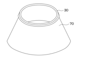
- the SiC single crystal manufacturing apparatus of this embodiment differs from the first embodiment in that the crucible 1 further has a skirt portion 70, as shown in FIG. 3, for example. This difference will be mainly described in this embodiment.
- the crucible 1 has, for example, a cylindrical protrusion 21 on the lid body 20, a skirt portion 70 surrounding the seed crystal 40 in the vicinity of the seed crystal 40 on the container body 10, and the seed crystal 40 is attached to the tip of the protrusion 21.
- the skirt portion 70 has a truncated cone shape with openings on the top and bottom, and the inner peripheral surface 70a is covered by the covering member 30.
- the skirt portion 70 has an opening with a smaller diameter between the top and bottom openings and is arranged near the seed crystal 40.
- the opening with a smaller diameter located on the upper bottom surface of the truncated cone shape of the skirt portion 70 may be referred to as the "small opening” and the opening with a larger diameter located on the lower bottom surface may be referred to as the "large opening”.
- the skirt portion 70 plays a role in expanding the diameter of the grown crystal when growing the SiC single crystal 60 on the seed crystal 40, and may also be referred to as, for example, a growth guide.
- the inclination angle of the inner peripheral surface 70a of the skirt portion 70 is the angle between a virtual line passing through the central axis of the upper and lower openings and the inner peripheral surface 70a, and is, for example, 45° or less.
- the skirt portion 70 is made of, for example, graphite, and the covering member 30 is fixed to the inner peripheral surface 70a.
- the covering member 30 attached to the skirt portion 70 is manufactured, for example, by the following process. For example, as shown in FIG. 5, a plate material 31 made of a metal material such as Ta and having a thickness of 0.1 mm to 3 mm is prepared, and the plate material 31 is deep-drilled to have a shape corresponding to the inner peripheral surface 70a of the skirt portion 70. Next, for example, a part of the plate material 31 is folded by a roll-tightening process to fix it to a small opening of the skirt portion 70, so that the plate material 31 covers the inner peripheral surface 70a of the skirt portion 70.
- a graphite member 100 having a shape that conforms to the inner peripheral surface 70a of the skirt portion 70 is prepared, and the plate material 31 attached to the skirt portion 70 is arranged adjacent to the graphite member 100.
- the plate material 31 is carbonized by heat treatment at 1500°C to 2500°C in an argon atmosphere to form a metal carbide with a melting point higher than the growth temperature of SiC.
- the skirt portion 70 has a configuration in which part or all of the inner circumferential surface 70a and the vicinity of the small opening are covered with the metal carbide coating member 30.
- the growth space 11 is surrounded by the inner wall surface 10a of the container body 10 and the inner peripheral surface 70a of the skirt portion 70. That is, in this embodiment, the side surface 12 is composed of the region of the inner wall surface 10a of the container body 10 from the large opening of the skirt portion 70 to the surface 50a of the raw material 50 and the inner peripheral surface 70a of the skirt portion 70.
- the covering member 30 covers a predetermined region of the side surface 12 from the height position 1A of the seed crystal 40 on the inner peripheral surface 70a toward the height position 1B so that the coverage rate of the side surface 12 is 5% to 80%.
- the covering member 30 may be arranged to cover a part of the inner peripheral surface 70a, or may be arranged to cover the entire area of the inner peripheral surface 70a or a part of the inner wall surface 10a in addition to the entire area of the inner peripheral surface 70a.
- the coverage range of the side surface 12 by the covering member 30 can be changed appropriately depending on the crystal height of the SiC single crystal 60 to be obtained.
- the SiC single crystal 60 is also obtained by growing within the area covered by the covering member 30, with the lower end of the covering member 30 on the side surface 12 being the upper limit of the crystal height.
- the SiC single crystal manufacturing apparatus and manufacturing method can obtain the same effect as the first embodiment.
- the crucible 1 has a skirt portion 70 in a truncated cone shape, and the small opening is arranged to match the height position 1A of the seed crystal 40, so that the SiC single crystal 60 can be grown to a diameter size larger than that of the seed crystal 40.
- FIG. 3 shows an example in which the upper end position of the covering member 30 covering the skirt portion 70 and the height position 1A of the surface 40a of the seed crystal 40 coincide, but this is not limited to this example, and these positions may be approximately the same.
- substantially coincident also includes cases where the covering member 30 is intentionally positioned so that the upper end position is higher or lower than the height position 1A, within a range that does not interfere with the growth of the SiC single crystal 60 on the surface 40a of the seed crystal 40.
- the skirt portion 70 may be positioned so that the upper end of the part covered by the covering member 30 coincides with the surface 40a of the seed crystal 40 in the height direction, may be positioned so that there is a gap between the surface 40a and the skirt portion 70, or may be positioned so that the skirt portion 70 overlaps the seed crystal 40.
- the SiC single crystal manufacturing apparatus of this embodiment differs from the first embodiment in that the crucible 1 has, in addition to the skirt portion 70, a support portion 80 and a baffle plate 81 extending from the bottom surface 10b of the container body 10.
- the skirt portion 70 is the same as in the second embodiment, so in this embodiment, the support portion 80 and the baffle plate 81 will be mainly described.
- the support part 80 is, for example, cylindrical and extends from the center of the bottom surface 10b of the container body 10 toward the opening side along the central axis of the crucible 1.
- the support part 80 is, for example, made of a material such as graphite that has a higher melting point than the raw material 50, just like the container body 10.
- the baffle plate 81 is, for example, disk-shaped and attached to the tip of the support 80.
- the baffle plate 81 is, for example, made of a material with a higher melting point than the growth temperature of SiC, such as graphite, like the support 80, and the upper surface 81a opposite to the lower surface 81b is covered with a coating material 82.
- the support 80 is connected to the center of the lower surface 81b on the bottom surface 10b side of the baffle plate 81, and plays a role in suppressing the inclusion of foreign matter from the raw material 50 when the SiC single crystal 60 is grown to a long length, i.e., until the crystal height becomes large.
- the baffle plate 81 is provided in the growth space 11 to block such foreign matter originating from the raw material 50 and suppress its inclusion into the SiC single crystal 60.
- the baffle plate 81 is disposed, for example, near the lower end of the covering member 30.
- the baffle plate 81 when the covering member 30 covers only a portion of the inner circumferential surface 70a of the skirt portion 70, the baffle plate 81 is disposed at a position closer to the seed crystal 40 than the large opening of the skirt portion 70.
- the height position of the baffle plate 81 may be set independently of the range covered by the covering member 30, and the entire area, not just the upper surface 81a, may be covered by the covering material 82.
- the coating material 82 is, for example, similar to the coating member 30, composed of a metal carbide with a melting point higher than the growth temperature of SiC.
- the coating material 82 is, for example, composed of a carbide of any one of tantalum, niobium, tungsten, and titanium.
- the coating material 82 is, for example, manufactured in a similar manner to the coating member 30, but the same material as the coating member 30 may be used, or a different material may be used.
- the support 80 and the baffle plate 81 are made of graphite, it is optional whether or not to cover the graphite parts of these components other than the top surface 81a with the coating material 82, and this is unrelated to the coverage rate of the side surface 12 by the coating material 30.
- a SiC single crystal manufacturing apparatus is provided with a crucible 1 that can achieve the same effects as the second embodiment.
- a baffle plate 81 whose upper surface 81a is covered with a coating material 82, foreign matter originating from the raw material 50 is prevented from being mixed into the SiC single crystal 60, resulting in a SiC single crystal manufacturing apparatus that can manufacture longer SiC single crystals 60.
- the SiC single crystal manufacturing apparatus of this embodiment has been described with an example in which the crucible 1 of the second embodiment has a support portion 80, a baffle plate 81, and a covering material 82, this is not limiting.
- the SiC single crystal manufacturing apparatus of this embodiment may have a configuration in which the crucible 1 of the first embodiment has a support portion 80, a baffle plate 81, and a covering material 82.
- the elements constituting the embodiment are not necessarily essential, except when it is specifically stated that they are essential or when it is clearly considered essential in principle.
- the numbers, values, amounts, ranges, etc. of the components of the embodiment are mentioned, they are not limited to the specific numbers, except when it is specifically stated that they are essential or when it is clearly limited to a specific number in principle.
- the shapes, positional relationships, etc. of the components, etc. are mentioned, they are not limited to the shapes, positional relationships, etc., except when it is specifically stated that they are essential or when it is clearly limited to a specific shape, positional relationship, etc. in principle.
- a method for producing a silicon carbide single crystal comprising the steps of: The method comprises the steps of: preparing a hollow cylindrical crucible (1) having a bottomed cylindrical container body (10), a lid (20) for closing an opening of the container body, and a covering member (30) made of a metal carbide having a higher melting point than silicon carbide and disposed inside the container body; a seed crystal (40) made of a silicon carbide substrate is placed on the lid, a silicon carbide raw material (50) is placed in the container body, and then a sublimation gas of the silicon carbide raw material is supplied to grow a silicon carbide single crystal (60) on the seed crystal, In preparing the crucible, a space in the crucible from a height position (1A) of a surface (40a) of the seed crystal to a height position (1B) of a surface (50a) of the silicon carbide raw material, in
- the covering member is made of a carbide of any one of tantalum, niobium, tungsten, and titanium.
- the step of preparing the crucible includes forming the covering member from tantalum carbide and setting a C/Ta ratio, which is a ratio of tantalum to carbon, within a range of 0.2 or more and 1 or less.
- preparing the crucible includes carbonizing a tantalum member (31), forming the covering member from tantalum carbide, and setting a rate of change in the weight and the dimensions of the tantalum member after the carbonization treatment to be 1% or more and 10% or less based on the weight and dimensions of the tantalum member before the carbonization treatment.
- preparing the crucible includes preparing a crucible further having a baffle (81) that is placed in the growth space, and whose upper surface (81 a) facing the seed crystal is covered with a covering material (82) made of a carbide having a melting point higher than that of silicon carbide.
- An apparatus for producing silicon carbide single crystals comprising: A cylindrical container body (10) with a bottom; A member to which a seed crystal (40) made of a silicon carbide substrate is attached, the member comprising a lid (20) for closing an opening of the container body; A crucible (1) having a covering member (30) made of a metal carbide having a melting point higher than a growth temperature of silicon carbide,
- the direction from the bottom surface (10b) of the crucible on which the silicon carbide raw material (50) is placed toward the lid body is defined as a height direction
- the position of the surface (50a) of the silicon carbide raw material in the crucible in the height direction is defined as a raw material height position (1B)
- the position of the surface (40a) of the seed crystal placed in the crucible in the height direction is defined as a seed crystal height position (1A)
- the space in the crucible from the raw material height position to the seed crystal height position and filled with sublimation gas of the silicon carbide raw material is defined as
- the silicon carbide single crystal manufacturing apparatus according to a ninth aspect, wherein the covering member covers an area of not less than 5% and not more than 80% of the side surface.
- the covering member is made of tantalum carbide and has a C/Ta ratio, which is a ratio of tantalum to carbon, in the range of 0.2 or more and 1 or less.
Landscapes
- Chemical & Material Sciences (AREA)
- Engineering & Computer Science (AREA)
- Crystallography & Structural Chemistry (AREA)
- Materials Engineering (AREA)
- Metallurgy (AREA)
- Organic Chemistry (AREA)
- Inorganic Chemistry (AREA)
- Crystals, And After-Treatments Of Crystals (AREA)
Priority Applications (1)
| Application Number | Priority Date | Filing Date | Title |
|---|---|---|---|
| CN202480060071.2A CN121889541A (zh) | 2023-09-22 | 2024-09-02 | 碳化硅单晶的制造方法及碳化硅单晶的制造装置 |
Applications Claiming Priority (2)
| Application Number | Priority Date | Filing Date | Title |
|---|---|---|---|
| JP2023159117A JP2025050363A (ja) | 2023-09-22 | 2023-09-22 | 炭化珪素単結晶の製造方法および炭化珪素単結晶の製造装置 |
| JP2023-159117 | 2023-09-22 |
Publications (1)
| Publication Number | Publication Date |
|---|---|
| WO2025063035A1 true WO2025063035A1 (ja) | 2025-03-27 |
Family
ID=95072793
Family Applications (1)
| Application Number | Title | Priority Date | Filing Date |
|---|---|---|---|
| PCT/JP2024/031477 Pending WO2025063035A1 (ja) | 2023-09-22 | 2024-09-02 | 炭化珪素単結晶の製造方法および炭化珪素単結晶の製造装置 |
Country Status (3)
| Country | Link |
|---|---|
| JP (1) | JP2025050363A (https=) |
| CN (1) | CN121889541A (https=) |
| WO (1) | WO2025063035A1 (https=) |
Citations (6)
| Publication number | Priority date | Publication date | Assignee | Title |
|---|---|---|---|---|
| JP2009051699A (ja) * | 2007-08-28 | 2009-03-12 | Denso Corp | 炭化珪素単結晶の製造装置 |
| JP2010018495A (ja) * | 2008-07-11 | 2010-01-28 | Denso Corp | 炭化珪素単結晶の製造装置の製造方法および炭化珪素単結晶の製造方法 |
| JP2011011926A (ja) * | 2009-06-30 | 2011-01-20 | Denso Corp | 炭化珪素単結晶の製造装置 |
| JP2011219336A (ja) * | 2010-04-14 | 2011-11-04 | Denso Corp | 炭化珪素単結晶の製造方法および製造装置 |
| JP2012201584A (ja) * | 2011-03-28 | 2012-10-22 | Showa Denko Kk | 炭化珪素単結晶製造装置、炭化珪素単結晶の製造方法及びその成長方法 |
| JP2015020938A (ja) * | 2013-07-22 | 2015-02-02 | 住友電気工業株式会社 | 炭化珪素結晶の製造装置、当該装置の製造方法、および当該装置を用いた炭化珪素結晶の製造方法 |
-
2023
- 2023-09-22 JP JP2023159117A patent/JP2025050363A/ja active Pending
-
2024
- 2024-09-02 CN CN202480060071.2A patent/CN121889541A/zh active Pending
- 2024-09-02 WO PCT/JP2024/031477 patent/WO2025063035A1/ja active Pending
Patent Citations (6)
| Publication number | Priority date | Publication date | Assignee | Title |
|---|---|---|---|---|
| JP2009051699A (ja) * | 2007-08-28 | 2009-03-12 | Denso Corp | 炭化珪素単結晶の製造装置 |
| JP2010018495A (ja) * | 2008-07-11 | 2010-01-28 | Denso Corp | 炭化珪素単結晶の製造装置の製造方法および炭化珪素単結晶の製造方法 |
| JP2011011926A (ja) * | 2009-06-30 | 2011-01-20 | Denso Corp | 炭化珪素単結晶の製造装置 |
| JP2011219336A (ja) * | 2010-04-14 | 2011-11-04 | Denso Corp | 炭化珪素単結晶の製造方法および製造装置 |
| JP2012201584A (ja) * | 2011-03-28 | 2012-10-22 | Showa Denko Kk | 炭化珪素単結晶製造装置、炭化珪素単結晶の製造方法及びその成長方法 |
| JP2015020938A (ja) * | 2013-07-22 | 2015-02-02 | 住友電気工業株式会社 | 炭化珪素結晶の製造装置、当該装置の製造方法、および当該装置を用いた炭化珪素結晶の製造方法 |
Also Published As
| Publication number | Publication date |
|---|---|
| JP2025050363A (ja) | 2025-04-04 |
| CN121889541A (zh) | 2026-04-17 |
Similar Documents
| Publication | Publication Date | Title |
|---|---|---|
| JP3961750B2 (ja) | 単結晶の成長装置および成長方法 | |
| JP4275308B2 (ja) | 炭化珪素単結晶の製造方法およびその製造装置 | |
| JP4962205B2 (ja) | 炭化珪素単結晶の製造方法および製造装置 | |
| JP6861555B2 (ja) | 炭化珪素単結晶インゴットの製造装置及び製造方法 | |
| JP4748067B2 (ja) | 炭化珪素単結晶の製造方法および製造装置 | |
| CN112334607B (zh) | 碳化硅单晶及其制造方法 | |
| JP5240100B2 (ja) | 炭化珪素単結晶の製造装置 | |
| JP2023127894A (ja) | 炭化珪素単結晶およびその製造方法 | |
| JP6628640B2 (ja) | 炭化珪素単結晶インゴットの製造装置及び製造方法 | |
| JP2011207691A (ja) | 炭化珪素単結晶の製造装置および炭化珪素単結晶の製造方法 | |
| WO2025063035A1 (ja) | 炭化珪素単結晶の製造方法および炭化珪素単結晶の製造装置 | |
| JP2015020938A (ja) | 炭化珪素結晶の製造装置、当該装置の製造方法、および当該装置を用いた炭化珪素結晶の製造方法 | |
| KR101633183B1 (ko) | 잉곳 제조 장치 | |
| JP6910168B2 (ja) | 炭化珪素単結晶インゴットの製造装置及び製造方法 | |
| JP6223290B2 (ja) | 単結晶の製造装置 | |
| JP4459211B2 (ja) | 単結晶の成長装置および成長方法 | |
| JP2009091173A (ja) | 炭化珪素単結晶の製造装置 | |
| JP5831339B2 (ja) | 炭化珪素単結晶の製造方法 | |
| JP4692394B2 (ja) | 炭化珪素単結晶の製造方法および製造装置 | |
| JP6317868B1 (ja) | 窒化アルミニウム単結晶製造装置 | |
| JP5327126B2 (ja) | 炭化珪素単結晶の製造方法および製造装置 | |
| JP4735622B2 (ja) | 炭化珪素単結晶の製造装置 | |
| JP5287675B2 (ja) | 炭化珪素単結晶の製造装置 | |
| JP2018030734A (ja) | 坩堝 | |
| JP6300990B1 (ja) | 窒化アルミニウム単結晶製造装置 |
Legal Events
| Date | Code | Title | Description |
|---|---|---|---|
| 121 | Ep: the epo has been informed by wipo that ep was designated in this application |
Ref document number: 24868114 Country of ref document: EP Kind code of ref document: A1 |