WO2025053187A1 - 縦型ダイオード及び縦型ダイオードの製造方法 - Google Patents
縦型ダイオード及び縦型ダイオードの製造方法 Download PDFInfo
- Publication number
- WO2025053187A1 WO2025053187A1 PCT/JP2024/031773 JP2024031773W WO2025053187A1 WO 2025053187 A1 WO2025053187 A1 WO 2025053187A1 JP 2024031773 W JP2024031773 W JP 2024031773W WO 2025053187 A1 WO2025053187 A1 WO 2025053187A1
- Authority
- WO
- WIPO (PCT)
- Prior art keywords
- electrode
- organic semiconductor
- semiconductor layer
- vertical diode
- weight hydrophobic
- Prior art date
- Legal status (The legal status is an assumption and is not a legal conclusion. Google has not performed a legal analysis and makes no representation as to the accuracy of the status listed.)
- Ceased
Links
Images







Classifications
-
- H—ELECTRICITY
- H10—SEMICONDUCTOR DEVICES; ELECTRIC SOLID-STATE DEVICES NOT OTHERWISE PROVIDED FOR
- H10D—INORGANIC ELECTRIC SEMICONDUCTOR DEVICES
- H10D8/00—Diodes
- H10D8/01—Manufacture or treatment
-
- H—ELECTRICITY
- H10—SEMICONDUCTOR DEVICES; ELECTRIC SOLID-STATE DEVICES NOT OTHERWISE PROVIDED FOR
- H10D—INORGANIC ELECTRIC SEMICONDUCTOR DEVICES
- H10D8/00—Diodes
- H10D8/50—PIN diodes
-
- H—ELECTRICITY
- H10—SEMICONDUCTOR DEVICES; ELECTRIC SOLID-STATE DEVICES NOT OTHERWISE PROVIDED FOR
- H10K—ORGANIC ELECTRIC SOLID-STATE DEVICES
- H10K10/00—Organic devices specially adapted for rectifying, amplifying, oscillating or switching; Organic capacitors or resistors having potential barriers
- H10K10/20—Organic diodes
Definitions
- This disclosure relates to a vertical diode and a method for manufacturing a vertical diode.
- Non-Patent Document 1 discloses a method for adjusting the work function of an electrode by coating the electrode with a polymer material such as polyethyleneimine.
- Non-Patent Document 2 discloses a method for adjusting the work function of an electrode by forming a thin film on the electrode using a material such as a polymer electrolyte and a tertiary aliphatic amine.
- a diode is a device that has rectification characteristics in which a current flows only in the forward direction and is difficult to flow in the reverse direction.
- diodes obtained by modifying the electrode surface by the methods described in Non-Patent Documents 1 and 2 may not have sufficient rectification characteristics, and improvement is desired.
- An object of the present disclosure is to provide a vertical diode having excellent rectification characteristics.
- the inventors have conducted extensive research. As a result, they have found that a vertical diode with excellent rectification characteristics can be obtained by using an electrode whose surface is modified with hydrophobic closed-shell ions. They have also found that a vertical diode with excellent rectification characteristics can be obtained by injecting carrier and dopant ions into an organic semiconductor in the vicinity of the electrode.
- the gist of the present disclosure is as follows.
- the low-molecular-weight hydrophobic ion is a low-molecular-weight hydrophobic closed-shell ion.
- the low molecular weight hydrophobic ion is a low molecular weight hydrophobic cation
- the low molecular weight hydrophobic ion is a low molecular weight hydrophobic anion
- each R 14 is independently a hydrogen atom, a halogen atom, or a fluorinated alkyl group which may have a substituent
- each R 15 is independently a perfluoroalkyl group, and two R 15s may be bonded to each other to form a ring.
- the small molecule hydrophobic ions form an ion layer on a surface of the first electrode adjacent to the organic semiconductor layer;
- the vertical diode according to any one of [1] to [5], wherein the thickness of the ion layer is 2 nm or less or a thickness of three molecular layers or less.
- a ratio of the low-molecular-weight hydrophobic ions forming a salt with a counter ion among the low-molecular-weight hydrophobic ions attached to a surface of the first electrode that is adjacent to the organic semiconductor layer is 25 mol % or less;
- the first electrode is a copper electrode.
- the low molecular weight hydrophobic ion is a low molecular weight hydrophobic cation
- the organic semiconductor layer has a doped layer and an undoped layer
- the vertical diode according to any one of [1] to [3] and [5] to [8], wherein the doped layer is a layer adjacent to the second electrode and contains holes and dopant anions.
- the low molecular weight hydrophobic ion is a low molecular weight hydrophobic anion
- the organic semiconductor layer has a doped layer and an undoped layer
- the vertical diode according to any one of [1] to [11] having a conversion efficiency from AC power at a frequency of 10 MHz to DC power of more than 5%.
- the method for producing a vertical diode, wherein the surface modifying liquid is any one of the following surface modifying liquids (S1) to (S4): (S1) a surface modifying liquid containing a first reducing agent that reduces the first electrode and generates a low-molecular-weight hydrophobic cation; (S2) a surface modifying liquid containing a
- the organic semiconductor layer has a doped layer and an undoped layer, the doped layer being adjacent to the second electrode; a doping step of contacting a surface of an organic semiconductor layer precursor with an aqueous solution containing one or more selected from the group consisting of a third oxidizing agent and a third reducing agent and a salt of a dopant ion, thereby forming the doped layer; a lamination step of laminating the organic semiconductor layer and the second electrode such that the doped layer and the second electrode are in contact with each other;
- a surface modification liquid for modifying a surface of an electrode and changing a work function of the electrode comprising:
- the surface modifying liquid is any one of the following surface modifying liquids (S1) to (S4).
- S1 A surface modification liquid containing a first reducing agent that reduces the electrode and generates a low-molecular-weight hydrophobic cation.
- S2 a surface modifying solution containing a first oxidizing agent that oxidizes the electrode and generates a low-molecular-weight hydrophobic anion.
- S3 A surface modification solution containing a second reducing agent that reduces the electrode and a low-molecular-weight hydrophobic closed-shell cation.
- (S4) A surface modification solution containing a second oxidizing agent that oxidizes the electrode and a low-molecular-weight hydrophobic closed-shell anion.
- the surface modifying liquid according to [22] wherein the surface modifying liquid (S2) further contains a low-molecular-weight hydrophobic anion different from the low-molecular-weight hydrophobic anion generated from the first oxidizing agent.
- a vertical diode including a first electrode, an organic semiconductor layer having a doped layer and an undoped layer, and a second electrode stacked adjacent to each other in this order, with the doped layer being adjacent to the first electrode or the second electrode, the doped layer includes carriers and dopant ions;
- the doped layer is adjacent to the second electrode, the carriers are holes, the dopant ion is a hydrophobic closed shell anion;
- the vertical diode according to claim 28, wherein a low-molecular-weight hydrophobic closed-shell cation is attached to a surface of the first electrode that is adjacent to the organic semiconductor layer.
- the doped layer is adjacent to the second electrode, the carriers are electrons, the dopant ion is a hydrophobic closed shell cation;
- a ratio of the dopant ions forming a salt with a counter ion to the dopant ions contained in the doped layer is 25 mol % or less;
- the fourth reducing agent is at least one selected from the group consisting of a hydroquinone compound having a hydroquinone skeleton and a reduced coenzyme, The method for producing a vertical diode according to [34], wherein the fourth oxidant is a quinone compound having a quinone skeleton.
- the doped layer is adjacent to the second electrode, The method further includes an electrode modification step of modifying a surface of the first electrode by contacting the surface of the first electrode with a surface modification liquid, The method for producing a vertical diode according to [34] or [35], wherein the surface modifying liquid is any one of the following surface modifying liquids (S1) to (S4).
- (S1) a surface modifying liquid containing a first reducing agent that reduces the first electrode and generates a low-molecular-weight hydrophobic cation;
- (S2) a surface modifying liquid containing a first oxidizing agent that oxidizes the first electrode and generates a low-molecular-weight hydrophobic anion.
- (S3) a surface modifying solution containing a second reducing agent that reduces the first electrode and a low-molecular-weight hydrophobic closed-shell cation.
- (S4) a surface modifying solution containing a second oxidizing agent for oxidizing the first electrode and a low-molecular-weight hydrophobic closed-shell anion.
- the present disclosure has the effect of providing a vertical diode with excellent rectification characteristics.
- the problems and advantages of the present disclosure are not limited to those specifically described above, but include those that will become apparent to those skilled in the art from the entire specification.
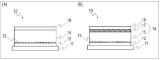
- FIG. 6 is a schematic cross-sectional view showing the structure of a vertical diode according to a second embodiment.
- FIG. 13 is a schematic cross-sectional view showing the structure of a vertical diode according to a fourth embodiment.
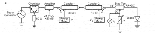
- FIG. 13 is a schematic diagram of a circuit used to evaluate 10% rectification at 1 GHz of the vertical diode prepared in Example 13.
- FIG. 13 is a diagram showing the evaluation results of 10% rectification at 1 GHz of the vertical diode produced in Example 13.
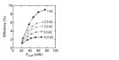
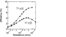
- FIG. 13 is a diagram showing the evaluation results of the conversion efficiency from AC power to DC power of the vertical diode fabricated in Example 6.
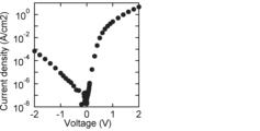
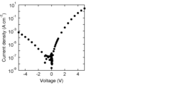
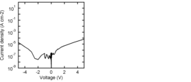
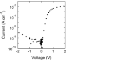
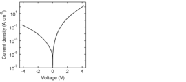
- FIG. 2 is a diagram showing the current-voltage characteristics of the vertical diode fabricated in Example 1.
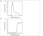
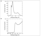
- FIG. 1 shows the results of UPS measurement of the surface-modified Cu electrode prepared in Example 2.
- FIG. 1 shows the results of UPS measurement of the unmodified Cu electrode prepared in Comparative Example 1.
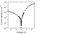
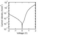
- FIG. 13 is a diagram showing the current-voltage characteristics of the vertical diode fabricated in Example 3.
- FIG. 13 is a diagram showing the current-voltage characteristics of the vertical diode fabricated in Example 4.
- FIG. 1 shows the results of UPS measurement of the surface-modified Cu electrode prepared in Example 2.
- FIG. 1 shows the results of UPS measurement of the unmodified Cu electrode prepared in Comparative Example 1.
- FIG. 13 is a diagram showing the current-voltage
- FIG. 13 is a diagram showing the current-voltage characteristics of the vertical diode fabricated in Example 5.
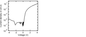
- FIG. 13 is a diagram showing the current-voltage characteristics of the vertical diode fabricated in Example 6.
- FIG. 13 is a diagram showing the current-voltage characteristics of the vertical diode fabricated in Example 7.
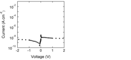
- FIG. 13 is a diagram showing the current-voltage characteristics of the vertical diode produced in Comparative Example 2.
- FIG. 13 is a diagram showing the current-voltage characteristics of the vertical diode produced in Comparative Example 3.
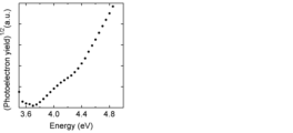
- FIG. 13 is a diagram showing the results of PYS measurement of the surface-modified ITO electrode prepared in Example 8.
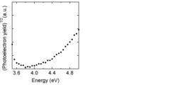
- FIG. 13 is a diagram showing the PYS measurement results of the unmodified ITO electrode prepared in Comparative Example 3.
- FIG. 13 is a diagram showing the PYS measurement results of the surface-modified ITO electrode prepared in Comparative Example 4.
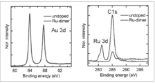
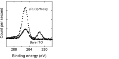
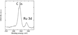
- FIG. 13 is a diagram showing the results of XPS elemental analysis of the unmodified ITO electrode prepared in Comparative Example 3.
- FIG. 13 is a diagram showing the results of XPS elemental analysis of the surface-modified ITO electrode prepared in Example 9.
- FIG. 13 is a diagram showing the results of XPS elemental analysis of the unmodified ITO electrode prepared in Comparative Example 5.
- FIG. 13 is a diagram showing the current-voltage characteristics of the vertical diode prepared in Example 10.
- FIG. 13 is a diagram showing the current-voltage characteristics of the vertical diode produced in Comparative Example 6.
- FIG. 13 is a diagram showing the current-voltage characteristics of the vertical diode prepared in Example 11.
- FIG. 13 is a diagram showing the current-voltage characteristics of the vertical diode prepared in Example 12.
- FIG. 13 is a diagram showing the current-voltage characteristics of the vertical diode prepared in Example 13.
- FIG. 13 is a diagram showing the evaluation results of the conversion efficiency from AC power to DC power of the vertical diode produced in Example 13.
- FIG. 15 is a diagram showing the current-voltage characteristics of the vertical diode prepared in Example 14.
- X to Y indicating a range means “X or more and Y or less.”
- a numerical range represented by “X to Y” or “X or more and Y or less” is described in stages (for example, in order of preference), the upper and lower limits of each numerical range can be combined in any combination.
- a description such as "X such as x1, x2, and x3" lists x1, x2, and x3 as examples of X, and does not mean that X is limited to x1, x2, x3, and the like.
- a first embodiment of the present disclosure is a method for manufacturing a vertical diode in which a first electrode, an organic semiconductor layer, and a second electrode are stacked adjacent to each other in this order.
- the manufacturing method according to this embodiment includes an electrode modification step of contacting a surface of a first electrode with a surface modification liquid to obtain a surface-modified first electrode; and a lamination step of laminating the first electrode and the organic semiconductor layer so that the surface of the first electrode modified in the electrode modification step comes into contact with the organic semiconductor layer.
- the surface modification liquid used in the electrode modification step is any one of surface modification liquids (S1) to (S4).
- S1 A surface modifying solution containing a first reducing agent that reduces a first electrode and produces low-molecular-weight hydrophobic cations.
- S2 A surface modifying solution containing a first oxidizing agent that oxidizes the first electrode and generates a low-molecular-weight hydrophobic anion.
- S3 A surface modification solution containing a second reducing agent that reduces the first electrode and a low-molecular-weight hydrophobic closed-shell cation.
- S4 A surface modification solution containing a second oxidant that oxidizes the first electrode and a low-molecular-weight hydrophobic closed-shell anion.
- hydrophobic means the property of having a low affinity for water and not dissolving or mixing in water, or being difficult to do so.
- hydrophobic ions refers to ions that contain one or more hydrophobic sites.
- hydrophobic sites include aromatic hydrocarbon groups having 5 to 20 carbon atoms, such as cyclopentadienyl groups and phenyl groups; aromatic heterocyclic groups having 3 to 20 carbon atoms, such as imidazolyl groups; hydrocarbon groups having 8 to 20 carbon atoms, such as octyl groups; fluorinated aliphatic hydrocarbon groups having 1 to 20 carbon atoms, such as trifluoromethyl and pentafluoroethyl groups, preferably perfluoroaliphatic hydrocarbon groups; and fluorinated aromatic hydrocarbon groups having 6 to 20 carbon atoms, such as pentafluorophenyl groups and heptafluoronaphthyl groups, preferably perfluoroaromatic hydrocarbon groups.
- the number of hydrophobic sites per molecule of the hydrophobic ion is preferably 1 to 10, more preferably 1 to 8, even more preferably 2 to 6, and particularly preferably 2 to 4.
- the ions become sufficiently bulky and exhibit hydrophobicity, resulting in a surface-modified electrode that is highly stable against water and air.
- a surface-modifying liquid containing a sufficient concentration of hydrophobic ions can be prepared.
- Hydrophobic ions are preferably ones in which the charge is widely delocalized within the hydrophobic ion. This is because the delocalization of the charge makes it possible to suppress local interactions with water, improving the hydrophobicity of the hydrophobic ion.
- the hydrophobic ion In order to delocalize the charge over a wide range of the hydrophobic ion, it is preferable for the hydrophobic ion to have a conjugated structure, an electron-withdrawing group (if the hydrophobic ion is a hydrophobic anion), an electron-donating group (if the hydrophobic ion is a hydrophobic cation), or the like.
- low molecular weight means that there is no molecular weight distribution and that the molecular weight is 2,000 or less, preferably 1,000 or less, more preferably 800 or less, and even more preferably 500 or less.
- molecules or ions that have a molecular weight distribution and have a molecular weight of 1,000 or more are distinguished by being called “macromolecules” or “polymers”.
- a vertical diode exhibiting excellent rectification characteristics can be obtained. Therefore, the manufacturing method according to this embodiment is useful as a method for manufacturing a rectifier diode.
- a rectifier diode has a feature that the current value in the forward direction is higher than that in the reverse direction, and the rectification ratio, which is the ratio, is two digits or more, preferably three digits or more.
- the degree of freedom in selecting the electrode material can be greatly improved.
- a vertical diode having excellent high frequency response or a vertical diode exhibiting high current density even at a low voltage can be obtained.
- current density means a forward current density.
- high current density at a low voltage means that the forward current density at a forward voltage of 2V is 1 Acm -2 or more, preferably 10 Acm -2 or more, more preferably 100 Acm -2 or more.
- the vertical diode obtained by the manufacturing method according to the present embodiment is considered to be applicable to various devices having a diode structure, such as solar cells and light-emitting diodes, and is also expected to be applied to electronic tags for wireless communication, which require high-frequency response.
- the electrode modification step is a step of modifying the surface of the first electrode by bringing the surface of the first electrode into contact with any one of the surface modifying solutions (S1) to (S4).
- the surface-modified first electrode is a first electrode on which low-molecular-weight hydrophobic ions are attached to the surface adjacent to the organic semiconductor layer when the vertical diode is fabricated.
- the work function of the first electrode can be significantly shifted by a simple solution process in which the surface of the first electrode is brought into contact with a surface modification liquid.
- the resulting electrode has low atmospheric stability, and when exposed to the atmosphere, the work function returns to approximately the same level as before the surface modification.
- the electrode modification step in this embodiment makes it possible to obtain a surface-modified electrode that is highly water-resistant and atmospherically stable. Therefore, as shown in the examples described below, even when the work function is measured after exposing the surface-modified electrode to the atmosphere, the work function that was shifted shallowly or deeply in the electrode modification step is maintained.
- the work function is the difference (positive value) between the Fermi level and the vacuum level.
- the Fermi level is the energy level at which the probability of electron occupancy is 0.5.
- the work function is equal to the ionization potential, which is the minimum energy required to extract one electron into a vacuum.
- the work function can be measured using an ultraviolet photoelectron spectrometer.
- the work function is a value measured using a photoelectron yield spectroscopy device for carrying out ionization potential measurement (for example, "AC-3" manufactured by Riken Keiki Co., Ltd.).
- the surface modifying liquids (S1) to (S4) for modifying the surface of the first electrode are preferably solutions or dispersions, more preferably solutions.
- the components contained in the surface modifying liquids (S1) to (S4) are described below.
- the first reducing agent contained in the surface modifying liquid (S1) is a compound that reduces the first electrode and generates low molecular weight hydrophobic cations.
- the surface modifying liquid (S1) is used as the surface modifying liquid, in this process, electrons are injected into the first electrode (i.e., the surface of the first electrode is reduced), thereby negatively charging the surface of the first electrode.
- low molecular weight hydrophobic cations generated from the first reducing agent are electrostatically attached to the surface of the negatively charged first electrode, and a first electrode with a modified surface is obtained.
- the low molecular weight hydrophobic cations are electrostatically attached to the first electrode to form a cationic layer.
- the thickness of the cationic layer is preferably three molecular layers or less, more preferably two molecular layers or less, and even more preferably a monolayer or less. In terms of specific thickness, the thickness of the cationic layer is preferably 2 nm or less, and more preferably 1 nm or less. The thickness of the cationic layer can be determined by X-ray photoelectron spectroscopy (XPS) analysis.
- the first reducing agent that generates low molecular weight hydrophobic cations is also a low molecular weight compound.
- the surface modification liquid (S1) preferably further contains low molecular weight hydrophobic cations (hereinafter, sometimes referred to as "other low molecular weight hydrophobic cations") different from the low molecular weight hydrophobic cations generated from the first reducing agent.
- other low molecular weight hydrophobic cations low molecular weight hydrophobic cations
- electrostatically adhere to the first electrode negatively charged by reduction or the low molecular weight hydrophobic cations derived from the first reducing agent electrostatically attached to the first electrode are replaced by the other low molecular weight hydrophobic cations.
- a cation layer is formed on the surface of the first electrode by the low molecular weight hydrophobic cations derived from the first reducing agent and the other low molecular weight hydrophobic cations, or the other low molecular weight hydrophobic cations.
- the molar ratio of the low molecular weight hydrophobic cations derived from the first reducing agent and the other low molecular weight hydrophobic cations in the cation layer can be adjusted by adjusting the concentration or degree of hydrophobicity of the other low molecular weight hydrophobic cations in the surface modification liquid (S1).
- low molecular weight hydrophobic cations derived from the first reducing agent and other low molecular weight hydrophobic cations may be collectively referred to as “low molecular weight hydrophobic cations" or “low molecular weight hydrophobic ions.”
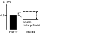
- the work function of the first electrode becomes shallower (smaller) than before modification.
- the shift in the work function of the first electrode due to the electrode modification process in this embodiment is very large; for example, as shown in the examples described later, the work function of a gold electrode shifts from approximately 5.0 eV to approximately 3.7 eV due to surface modification.
- the electron injection from the first electrode to the organic semiconductor layer is greatly improved.
- electrons can easily enter the LUMO of the organic semiconductor from the first electrode, and therefore can easily move from the first electrode through the organic semiconductor layer to the second electrode.
- the electron injection from the second electrode to the organic semiconductor layer is hardly changed, and the movement of electrons from the second electrode to the first electrode is more difficult than the movement of electrons from the first electrode to the second electrode.
- the surface modification of the first electrode makes it easier for current to flow from the second electrode to the first electrode, and the ease of current flow from the first electrode to the second electrode is hardly changed, and therefore the rectification characteristics of the vertical diode are improved, and the stable operation of the vertical diode can be realized. It is also possible to increase the current density of the vertical diode at low voltage.
- a vertical diode with excellent rectification characteristics can be obtained by using a layer of an electron transporting organic semiconductor, i.e., a layer of an n-type organic semiconductor, as the organic semiconductor layer and using the first electrode as an electron injection electrode (cathode (negative pole)). Also, a vertical diode that exhibits high current density even at low voltage can be obtained. In this case, it is not necessary for the entire organic semiconductor layer to be an n-type organic semiconductor layer; for example, when the organic semiconductor layer has a multi-layer structure, the above effect can be obtained as long as only the layer adjacent to the first electrode is an n-type organic semiconductor layer.
- a method of adjusting the work function of an electrode by depositing a polymer or salt on the electrode is known.
- a polymer layer thicker than a monolayer is formed between the electrode and the organic semiconductor layer, which causes a problem of significantly reducing the electron injection from the electrode to the organic semiconductor layer.
- a salt of a cationic species and a counter anion such as a halide ion is used as the salt to be deposited on the electrode.
- This salt not only reduces the electron injection from the electrode to the organic semiconductor layer, but also causes the problem that the halide ions diffuse into the organic semiconductor layer, reducing the life of the device.
- both the polymer and the salt contain parts other than those responsible for controlling the work function, even when these materials are deposited thinly, so that it is inevitable that an excess function that hinders electron injection occurs.
- the manufacturing method according to this embodiment has an advantage in principle in semiconductor element manufacturing.
- low molecular weight hydrophobic cations are attached (adsorbed) to the surface of the negatively charged first electrode by a reduction reaction to form a thin cation layer, effectively suppressing the formation of an excess layer that inhibits electron transfer between the first electrode and the organic semiconductor layer, or the formation of salt. Therefore, in addition to excellent electron transfer between the first electrode and the organic semiconductor layer and the rectification characteristics of the vertical diode, it is also possible to achieve a longer life for the vertical diode and improved current density at low voltage.
- the first reducing agent is not particularly limited as long as it produces electrons and low molecular weight hydrophobic cations and can reduce the first electrode.
- the low molecular weight hydrophobic cation generated from the first reducing agent is preferably a low molecular weight hydrophobic cation that is highly hydrophobic and stable against air and water, and is more preferably a low molecular weight hydrophobic closed shell cation. This is because low molecular weight hydrophobic closed shell cations are highly stable in solvents, particularly in water.
- low molecular weight hydrophobic cations generated from the first reducing agent include low molecular weight hydrophobic closed shell cations represented by formulas (1A) to (1C).
- the low molecular weight hydrophobic cations generated from the first reducing agent are preferably one or more types selected from the cations represented by formulas (1A) to (1B), and more preferably one or more types selected from the cation represented by formula (1B) in terms of higher stability to air and water.
- M1 is rhodium or iridium, preferably rhodium.
- M2 is ruthenium
- M3 is cobalt.
- R 1 to R 3 each independently represent a hydrogen atom, an alkyl group which may have a substituent, or an aryl group which may have a substituent.
- R 1 is preferably a hydrogen atom or an alkyl group which may have a substituent, and more preferably a hydrogen atom or an unsubstituted alkyl group.
- R2 is preferably a hydrogen atom or an alkyl group which may have a substituent, and more preferably a hydrogen atom or an unsubstituted alkyl group.
- R3 is preferably a hydrogen atom or an alkyl group which may have a substituent, and more preferably a hydrogen atom or an unsubstituted alkyl group.
- substituents that the alkyl and aryl groups represented by R 1 to R 3 may have include, but are not limited to, a deuterium atom; a hydroxyl group; a halogen atom such as a fluorine atom, a chlorine atom, or a bromine atom; an alkyl group having 1 to 4 carbon atoms, such as a methyl group, an ethyl group, an n-propyl group, or an isopropyl group; a cycloalkyl group such as a cyclopropyl group or a cyclobutyl group; an aryl group having 6 to 12 carbon atoms, such as a phenyl group, a 1-naphthyl group, or a 2-naphthyl group; and an aralkyl group such as a benzyl group or a 2-phenylethyl group.
- the number of carbon atoms of the alkyl group which may have a substituent represented by R 1 to R 3 is not particularly limited, but is preferably 1 or more and 20 or less, more preferably 1 or more and 12 or less, even more preferably 2 or more and 8 or less, and particularly preferably 2 or more and 6 or less.
- alkyl group which may have a substituent and which are represented by R 1 to R 3 include a methyl group, an ethyl group, an n-propyl group, an isopropyl group, an n-butyl group, a sec-butyl group, a tert-butyl group, an isobutyl group, an n-pentyl group, an isopentyl group, a neopentyl group, an n-hexyl group, a trifluoromethyl group, a pentafluoroethyl group, a hydroxymethyl group, and a 2-hydroxyethyl group, and preferably a methyl group.
- the number of carbon atoms of the aryl group which may have a substituent and is represented by R 1 to R 3 is not particularly limited, but is preferably 6 or more and 20 or less, and more preferably 6 or more and 14 or less.
- low molecular weight hydrophobic closed shell cations represented by formula (1A) include the following cations.
- low molecular weight hydrophobic closed shell cations represented by formula (1B) include the following cations.
- low molecular weight hydrophobic closed shell cations represented by formula (1C) include the following cations.
- Examples of the first reducing agent that produces these low molecular weight hydrophobic cations include compounds represented by formulas (2A) to (2C).
- the compounds represented by formulas (2A) to (2C) are first reducing agents that produce low molecular weight hydrophobic closed shell cations represented by formulas (1A) to (1C), respectively. Therefore, of these, the first reducing agent is preferably one or more types selected from the compounds represented by formulas (2A) to (2B), and more preferably one or more types selected from the compounds represented by formula (2B) in that it can produce low molecular weight hydrophobic closed shell cations that are more stable to air and water.
- M1 and R1 in formula (2A) have the same meanings as M1 and R1 in formula (1A), and preferred embodiments thereof are also the same.
- M2 and R2 in formula (2B) have the same meanings as M2 and R2 in formula (1B), and preferred embodiments thereof are also the same.
- M3 and R3 in formula (2C) have the same meanings as M3 and R3 in formula (1C), and preferred embodiments thereof are also the same.
- compounds represented by formula (2C) include cobaltocene and decamethylcobaltocene.
- the first reducing agent may be used alone or in any combination of two or more kinds in any ratio. Therefore, the low molecular weight hydrophobic cation attached to the surface of the first electrode may also be one type or two or more types.
- the other low molecular weight hydrophobic cations contained in the surface modification liquid (S1) are synonymous with the low molecular weight hydrophobic cations derived from the first reducing agent, and the preferred embodiments are also the same.
- the low molecular weight hydrophobic cations may be used alone or in any ratio and combination of two or more.
- the other low molecular weight hydrophobic cations contained in one surface modification liquid (S1) are cations different from the low molecular weight hydrophobic cations derived from the first reducing agent.
- the counter anion of the other low molecular weight hydrophobic cation contained in the surface modification liquid (S1) is not particularly limited, but may be, for example, a hydroxide ion; halide ions such as chloride ions, bromide ions, and iodide ions; carbonate ions; sulfate ions; and phosphate ions.
- the counter anion is preferably a hydroxide ion, since it can suppress the deposition of halide salts that inhibit electron injection from the first electrode to the organic semiconductor layer.
- the total concentration of the first reducing agent in the surface modification liquid (S1) is not particularly limited and may be appropriately selected depending on the type of the first reducing agent, the coverage of the low-molecular-weight hydrophobic ion described below, the shift width of the work function, etc.
- the total concentration of the first reducing agent is preferably 0.01% by mass or more and 3.00% by mass or less, more preferably 0.10% by mass or more and 1.00% by mass or less.
- the total concentration of the other low molecular weight hydrophobic cations in the surface modification liquid (S1) is not particularly limited and may be appropriately selected depending on the type of other low molecular weight hydrophobic cations, the low molecular weight hydrophobic ion coverage rate described below, the shift width of the work function, and the proportion of the other low molecular weight hydrophobic cations in all the low molecular weight hydrophobic cations modifying the first electrode.
- the total concentration of the low molecular weight hydrophobic cations is preferably 0.01 mass% or more and 3.00 mass% or less, more preferably 0.10 mass% or more and 1.00 mass% or less.
- the first oxidizing agent contained in the surface modifying liquid (S2) is a compound that oxidizes the first electrode and generates low molecular weight hydrophobic anions.
- the surface modifying liquid (S2) is used as the surface modifying liquid, in this process, holes are injected into the first electrode (i.e., the surface of the first electrode is oxidized), thereby positively charging the surface of the first electrode.
- low molecular weight hydrophobic anions generated from the first oxidizing agent are electrostatically attached to the surface of the positively charged first electrode, and a first electrode having a modified surface is obtained. At this time, the low molecular weight hydrophobic anions are electrostatically attached to the first electrode to form an anion layer.
- the thickness of the anion layer is preferably three molecular layers or less, more preferably two molecular layers or less, and even more preferably a monolayer or less. In terms of specific thickness, the thickness of the anion layer is preferably 2 nm or less, and more preferably 1 nm or less.
- the thickness of the anion layer can be determined by X-ray photoelectron spectroscopy (XPS) analysis.
- the first oxidizing agent that generates a low-molecular-weight hydrophobic anion is also a low-molecular-weight compound.
- the surface modification liquid (S2) preferably further contains low molecular weight hydrophobic anions (hereinafter, sometimes referred to as "other low molecular weight hydrophobic anions") different from the low molecular weight hydrophobic anions generated from the first oxidizing agent.
- other low molecular weight hydrophobic anions low molecular weight hydrophobic anions
- the other low molecular weight hydrophobic anions electrostatically adhere to the first electrode positively charged by oxidation, or the low molecular weight hydrophobic anions derived from the first oxidizing agent electrostatically attached to the first electrode are replaced by the other low molecular weight hydrophobic anions.
- an anion layer is formed on the surface of the first electrode by the low molecular weight hydrophobic anions derived from the first oxidizing agent and the other low molecular weight hydrophobic anions, or the other low molecular weight hydrophobic anions.
- the molar ratio of the low molecular weight hydrophobic anions derived from the first oxidizing agent and the other low molecular weight hydrophobic anions in the anion layer can be controlled by adjusting the concentration or degree of hydrophobicity of the low molecular weight hydrophobic anions in the surface modification liquid (S2).
- low molecular weight hydrophobic anions derived from the first oxidizing agent and other low molecular weight hydrophobic anions may be collectively referred to as “low molecular weight hydrophobic anions" or “low molecular weight hydrophobic ions.”
- the work function of the first electrode becomes deeper (larger) than before modification. According to the electrode modification process in this embodiment, the work function of the first electrode can be significantly shifted.
- the hole injection from the first electrode to the organic semiconductor layer is greatly improved.
- holes can be easily injected from the first electrode into the HOMO of the organic semiconductor, and can easily move from the first electrode through the organic semiconductor layer to the second electrode.
- the hole injection from the second electrode to the organic semiconductor layer is hardly changed, and the movement of holes from the second electrode to the first electrode is more difficult than the movement of holes from the first electrode to the second electrode.
- the surface modification of the first electrode makes it easier for current to flow from the first electrode to the second electrode, and the ease of current flow from the second electrode to the first electrode is hardly changed, and therefore the rectification characteristics of the vertical diode are improved, and the stable operation of the vertical diode can be realized. It is also possible to increase the current density of the vertical diode at low voltage.
- a vertical diode with excellent rectification characteristics can be obtained by using a hole-transporting organic semiconductor layer, i.e., a p-type organic semiconductor layer, as the organic semiconductor layer and using the first electrode as a hole injection electrode (anode (positive electrode)). Also, a vertical diode that exhibits high current density even at low voltage can be obtained. In this case, it is not necessary for the entire organic semiconductor layer to be a p-type organic semiconductor layer; for example, when the organic semiconductor layer has a multi-layer structure, the above effect can be similarly obtained as long as only the layer adjacent to the first electrode is a p-type organic semiconductor layer.
- the low molecular weight hydrophobic anion generated from the first oxidizing agent is preferably a low molecular weight hydrophobic anion that is highly hydrophobic and stable against air and water, more preferably a low molecular weight hydrophobic closed shell anion or a low molecular weight hydrophobic radical anion, and even more preferably a low molecular weight hydrophobic closed shell anion. This is because low molecular weight hydrophobic closed shell anions are highly stable in solvents, particularly in water.
- low molecular weight hydrophobic closed shell anions generated from the first oxidizing agent include FeCl 4 -- and the anions represented by formulae (3A) to (3C).
- each R 11 is independently a trifluoromethyl group (CF 3 ), a methyloxycarbonyl group (COOMe), or a trifluoromethyloxycarbonyl group (COOCF 3 ).
- R 12 each independently represents a hydrogen atom, a halogen atom, or an alkyl group which may have a substituent, is preferably a hydrogen atom or a halogen atom, and is more preferably a halogen atom.
- Examples of the halogen atom represented by R 12 include a fluorine atom, a chlorine atom, a bromine atom, and an iodine atom, and a fluorine atom is preferred.
- the alkyl group which may have a substituent represented by R 12 has the same meaning as the alkyl group which may have a substituent represented by R 1 to R 3 , and the preferred embodiments thereof are also the same.
- each R 13 is independently a cyano group (CN) or a methyloxycarbonyl group (COOMe).
- Examples of the first oxidizing agent that generates a low-molecular-weight hydrophobic closed-shell anion include iron(III) chloride and the compounds represented by formulae (4A) to (4C).
- Iron(III) chloride is a first oxidizing agent that generates FeCl 4 -
- the compounds represented by formulae (4A) to (4C) are first oxidizing agents that generate low-molecular-weight hydrophobic closed-shell cations represented by formulae (3A) to (3C), respectively.
- R 11 in formula (4A) has the same meaning as R 11 in formula (3A), and the preferred embodiments thereof are also the same.
- R 12 in formula (4B) has the same meaning as R 12 in formula (3B), and the preferred embodiments thereof are also the same.
- R 13 in formula (4C) has the same meaning as R 13 in formula (3C), and the preferred embodiments thereof are also the same.
- Examples of the low molecular weight hydrophobic radical anion generated from the first oxidizing agent include radical anions represented by formulas (3D) to (3E). Of these, it is preferable that the low molecular weight hydrophobic radical anion generated from the first oxidizing agent is one or more types selected from the radical anion represented by formula (3D).
- R 14 and R 15 each independently represent a hydrogen atom, a halogen atom, or an alkyl group which may have a substituent, preferably a hydrogen atom or a halogen atom, more preferably a halogen atom.
- Examples of the halogen atom represented by R 14 and R 15 include a fluorine atom, a chlorine atom, a bromine atom, and an iodine atom, and a fluorine atom is preferred.
- the alkyl group which may have a substituent represented by R 14 and R 15 has the same meaning as the alkyl group which may have a substituent represented by R 1 to R 3 , and the preferred embodiments thereof are also the same.
- low molecular weight hydrophobic radical anions represented by formula (3D) include the following anions.
- low molecular weight hydrophobic radical anion represented by formula (3E) include the following anions.
- First oxidizing agents that generate low molecular weight hydrophobic radical anions include compounds represented by formulas (4D) to (4E).
- the compounds represented by formulas (4D) to (4E) are first oxidizing agents that generate low molecular weight hydrophobic radical cations represented by formulas (3D) to (3E), respectively. Therefore, of these, it is preferable that the first oxidizing agent is one or more types selected from the compounds represented by formula (4D).
- R 14 in formula (4D) has the same meaning as R 14 in formula (3D), and the preferred embodiments thereof are also the same.
- R 15 in formula (4E) has the same meaning as R 15 in formula (3E), and the preferred embodiments thereof are also the same.
- the first oxidizing agent may be used alone or in any combination of two or more kinds in any ratio. Accordingly, the low molecular weight hydrophobic anion attached to the surface of the first electrode may also be one type or two or more types.
- the other low molecular weight hydrophobic anion contained in the surface modification liquid (S2) is synonymous with the low molecular weight hydrophobic anion derived from the first oxidizing agent, and the preferred embodiments are also the same.
- the low molecular weight hydrophobic anion may be used alone or in any ratio and combination of two or more types.
- the other low molecular weight hydrophobic anion contained in one surface modification liquid (S2) is an anion different from the low molecular weight hydrophobic anion derived from the first reducing agent.
- the counter cation of the other low molecular weight hydrophobic anion contained in the surface modification liquid (S2) is not particularly limited, but may be, for example, a proton; or a metal ion such as a lithium ion, a sodium ion, or a potassium ion.
- the counter cation is preferably a proton, since it can suppress the deposition of metal salts that inhibit hole injection from the first electrode to the organic semiconductor layer.
- the total concentration of the first oxidizing agent in the surface modification liquid (S2) is not particularly limited and may be appropriately selected depending on the type of first oxidizing agent, the coverage of low-molecular-weight hydrophobic ions described below, the shift width of the work function, and the like.
- the total concentration of the first oxidizing agent is preferably 0.01% by mass or more and 3.00% by mass or less, and more preferably 0.10% by mass or more and 1.00% by mass or less.
- the total concentration of the other low molecular weight hydrophobic anions in the surface modification liquid (S2) is not particularly limited and may be appropriately selected depending on the type of the other low molecular weight hydrophobic anions, the low molecular weight hydrophobic ion coverage rate described below, the shift width of the work function, and the proportion of the other low molecular weight hydrophobic anions in the total low molecular weight hydrophobic anions modifying the first electrode.
- the total concentration of the low molecular weight hydrophobic anions is preferably 0.01% by mass or more and 3.00% by mass or less, more preferably 0.10% by mass or more and 1.00% by mass or less.
- the second reducing agent contained in the surface modifying liquid (S3) is a compound that reduces the first electrode and does not generate low molecular weight hydrophobic cations. Moreover, the second reducing agent is preferably a compound that does not generate any cationic species other than the low molecular weight hydrophobic cations during the reduction of the first electrode. This is because the second reducing agent does not generate any cationic species, and thus the low molecular weight hydrophobic closed shell cations contained in the surface modifying liquid (S3) can be selectively attached to the surface of the first electrode.
- the second reducing agent the same as the third reducing agent described later can be used, and compounds that are preferred as the third reducing agent are also preferred as the second reducing agent. That is, examples of the second reducing agent include hydroquinone compounds having a hydroquinone skeleton, which are described later as the third reducing agent; dihydroxyfuranone compounds having a dihydroxyfuranone skeleton; sugars having reducing properties; and reduced coenzymes; and the like.
- the second reducing agent is preferably one or more selected from the group consisting of hydroquinone compounds having a hydroquinone skeleton and reduced coenzymes, and more preferably a reduced coenzyme.
- the low molecular weight hydrophobic closed shell cation contained in the surface modification liquid (S3) is one that is unlikely to undergo an oxidation-reduction reaction with water or an oxidation-reduction reaction with oxygen under temperature conditions of 15°C or higher and 35°C or lower (room temperature conditions) and in the air.
- Such low molecular weight hydrophobic closed shell cations are preferably those represented by formulas (1D) to (1F) in addition to the low molecular weight hydrophobic closed shell cations generated from the first reducing agent.
- R 4 to R 6 each independently represent a hydrogen atom, an alkyl group which may have a substituent, or an aryl group which may have a substituent.
- the alkyl group which may have a substituent and the aryl group which may have a substituent represented by R4 to R6 have the same meaning as the alkyl group which may have a substituent and the aryl group which may have a substituent represented by R1 to R3, respectively.
- R4 is preferably an alkyl group which may have a substituent or an aryl group which may have a substituent, more preferably an aryl group which may have a substituent, and further preferably an unsubstituted aryl group.
- R5 is preferably an alkyl group which may have a substituent or an aryl group which may have a substituent, more preferably an aryl group which may have a substituent, and further preferably an unsubstituted aryl group.
- R6 is preferably an alkyl group which may have a substituent or an aryl group which may have a substituent, and more preferably an unsubstituted alkyl group or an aryl group which may have a substituent.
- low molecular weight hydrophobic closed shell cations represented by formula (1D) include the following cations.
- low molecular weight hydrophobic closed shell cations represented by formula (1E) include the following cations.
- low molecular weight hydrophobic closed shell cations represented by formula (1F) include the following cations.
- the counter anion of the low molecular weight hydrophobic closed shell cation contained in the surface modification liquid (S3) is not particularly limited, but examples thereof include hydroxide ions; halide ions such as chloride ions, bromide ions, and iodide ions; carbonate ions; sulfate ions; and phosphate ions.
- the counter anion is preferably a hydroxide ion, since it can suppress the deposition of halide salts that inhibit electron injection from the first electrode to the organic semiconductor layer.
- the total concentration of the second reducing agent in the surface modification liquid (S3) is not particularly limited and may be appropriately selected depending on the type of the second reducing agent and the shift width of the work function.
- the total concentration of the second reducing agent is preferably 0.01% by mass or more and 3.00% by mass or less, and more preferably 0.10% by mass or more and 1.00% by mass or less.
- the total concentration of low molecular weight hydrophobic closed shell cations in the surface modification liquid (S3) is not particularly limited and may be appropriately selected depending on the type of low molecular weight hydrophobic closed shell cation, the low molecular weight hydrophobic ion coverage rate described below, and the shift width of the work function.
- the total concentration of low molecular weight hydrophobic closed shell cations is preferably 0.01 mass% or more and 3.00 mass% or less, more preferably 0.10 mass% or more and 1.00 mass% or less.
- the total concentration of the halide ions in the surface modification liquid (S3) is preferably 100 ppm by mass or less, more preferably 10 ppm by mass or less, and even more preferably 1 ppm by mass or less.
- the surface modification liquid (S3) is used as the surface modification liquid, in this process, electrons are injected into the first electrode (i.e., the surface of the first electrode is reduced), causing the surface of the first electrode to become negatively charged. Then, low molecular weight hydrophobic closed shell cations are electrostatically attached to the negatively charged surface of the first electrode, resulting in a surface-modified first electrode. At this time, as in the case of using the surface modification liquid (S1), low molecular weight hydrophobic closed shell cations are electrostatically attached to the surface of the first electrode, forming a cationic layer with a thickness of less than a monolayer. The thickness of the cationic layer can be determined by X-ray photoelectron spectroscopy (XPS) analysis.
- XPS X-ray photoelectron spectroscopy
- the surface modification liquid (S3) when used as the surface modification liquid, the surface of the first electrode is modified in the same way as when the surface modification liquid (S1) is used. Therefore, when the surface modification liquid (S3) is used as the surface modification liquid, the work function of the first electrode can be made shallow (small) in the same way as when the surface modification liquid (S1) is used, and the rectification characteristics of the vertical diode can be improved. It is also possible to increase the current density of the vertical diode at low voltages.
- a vertical diode with excellent rectification characteristics can be obtained by using an electron transporting organic semiconductor layer, i.e., an n-type organic semiconductor layer, as the organic semiconductor layer and using the first electrode as an electron injection electrode (cathode (negative pole)). Also, a vertical diode that exhibits high current density even at low voltage can be obtained. In this case, it is not necessary for the entire organic semiconductor layer to be an n-type organic semiconductor layer; for example, when the organic semiconductor layer has a multi-layer structure, the above effect can be obtained as long as only the layer adjacent to the first electrode is an n-type organic semiconductor layer.
- the second oxidizing agent contained in the surface modifying liquid (S4) is a compound that oxidizes the first electrode and does not generate low molecular weight hydrophobic anions. Moreover, the second oxidizing agent is preferably a compound that does not generate any anion species other than the low molecular weight hydrophobic anions during the oxidation of the first electrode. This is because the second oxidizing agent does not generate any anion species, and thus the low molecular weight hydrophobic closed shell anions contained in the surface modifying liquid (S4) can be selectively attached to the surface of the first electrode.
- the second oxidizing agent the same as the third oxidizing agent described later can be used, and compounds that are preferred as the third oxidizing agent are also preferred as the second oxidizing agent.
- examples of the second oxidizing agent include quinone compounds having a quinone skeleton, which are described later as the third oxidizing agent; furantrione compounds having a furantrione skeleton; and radical compounds; and the like, with quinone compounds having a quinone skeleton being preferred.
- the low molecular weight hydrophobic closed shell anion contained in the surface modification liquid (S4) is one that is unlikely to undergo an oxidation-reduction reaction with water or an oxidation-reduction reaction with oxygen under temperature conditions of 15°C or higher and 35°C or lower (room temperature conditions) and in the air.
- Such low molecular weight hydrophobic closed shell anions are preferably those represented by formulae (3F) to (3G) in addition to the low molecular weight hydrophobic closed shell anions generated from the first oxidizing agent.
- R 14 is each independently a hydrogen atom, a halogen atom, or an optionally substituted fluorinated alkyl group, and is preferably a halogen atom.
- each R 15 is independently a perfluoroalkyl group, and two R 15s may be linked to each other to form a ring.
- Examples of the halogen atom represented by R 14 include a fluorine atom, a chlorine atom, a bromine atom, and an iodine atom, and preferably a chlorine atom or a fluorine atom, and more preferably a fluorine atom.
- Examples of the substituent that the fluorinated alkyl group represented by R 14 may have include, but are not limited to, the same as the substituent that the alkyl group and aryl group represented by R 1 to R 3 may have. Note that in the fluorinated alkyl group, the substituent is a group that replaces a hydrogen atom bonded to a carbon atom of the fluorinated alkyl group.
- the number of carbon atoms of the fluorinated alkyl group which may have a substituent and is represented by R 14 is not particularly limited, but is preferably 1 or more and 10 or less, more preferably 1 or more and 6 or less, and further preferably 2 or more and 4 or less.
- fluorinated alkyl group which may have a substituent represented by R 14 include a trifluoromethyl group, a pentafluoroethyl group, a pentafluoro-n-propyl group, and a 1,1,1,3,3,3-hexafluoro-2-methoxy-2-propyl group, and preferably a trifluoromethyl group.
- the number of carbon atoms in the perfluoroalkyl group represented by R 15 is not particularly limited, but is preferably 1 to 20, more preferably 1 to 12, even more preferably 2 to 8, and particularly preferably 2 to 6.
- perfluoroalkyl group represented by R 15 examples include a perfluoromethyl group (a trifluoromethyl group), a perfluoroethyl group, a perfluoro-n-propyl group, a perfluoroisopropyl group, a perfluoro-n-butyl group, a perfluoroisobutyl group, a perfluoro-sec-butyl group, a perfluoro-tert-butyl group, a perfluoro-n-pentyl group, a perfluoroneopentyl group, a perfluoro-n-hexyl group, a perfluorocyclohexyl group, and the like, and preferred are a perfluoromethyl group and a perfluoro-n-butyl group.
- low molecular weight hydrophobic closed shell anions represented by formula (3F) include tetraphenylborate anion, tetrakis(p-tolyl)borate anion, tetrakis(p-trifluoromethylphenyl)borate anion, tetrakis(p-fluorophenyl)borate anion, tetrakis(perfluorophenyl)borate anion, and tetrakis[3,5-bis(trifluoromethyl)phenyl]borate anion, with tetrakis[3,5-bis(trifluoromethyl)phenyl]borate anion being preferred.
- low molecular weight hydrophobic closed shell anions represented by formula (3G) include bis(trifluoromethanesulfonyl)imide anion, bis(perfluoroethanesulfonyl)imide anion, bis(perfluoropropanesulfonyl)imide anion, bis(perfluorobutanesulfonyl)imide anion, and cyclohexafluoropropane-1,3-bis(sulfonyl)imide anion, with bis(trifluoromethanesulfonyl)imide anion being preferred.
- the counter cation of the low molecular weight hydrophobic closed shell anion contained in the surface modification liquid (S4) is not particularly limited, but examples include protons and metal ions such as lithium ions, sodium ions, and potassium ions. Of these, the counter cation is preferably a proton, since it can suppress the deposition of metal salts that inhibit hole injection from the first electrode to the organic semiconductor layer.
- the total concentration of the metal ion in the surface modification liquid (S3) is preferably 10,000 mass ppm or less, more preferably 1,000 mass ppm or less, and even more preferably 100 mass ppm or less.
- the total concentration of the second oxidizing agent in the surface modification liquid (S4) is not particularly limited and may be appropriately selected depending on the type of second oxidizing agent and the shift width of the work function.
- the total concentration of the second oxidizing agent is preferably 0.01% by mass or more and 3.00% by mass or less, and more preferably 0.10% by mass or more and 1.00% by mass or less.
- the total concentration of the low molecular weight hydrophobic closed shell anions in the surface modification liquid (S4) is not particularly limited and may be appropriately selected depending on the type of low molecular weight hydrophobic closed shell anions, the low molecular weight hydrophobic ion coverage rate described below, the shift width of the work function, etc.
- the total concentration of the low molecular weight hydrophobic closed shell anions is preferably 0.01 mass% or more and 3.00 mass% or less, more preferably 0.10 mass% or more and 1.00 mass% or less.
- the surface modification liquid (S4) is used as the surface modification liquid, in this process, holes are injected into the first electrode (i.e., the surface of the first electrode is oxidized), so that the surface of the first electrode becomes positively charged. Then, low molecular weight hydrophobic closed shell anions are electrostatically attached to the surface of this positively charged first electrode, and a surface-modified first electrode is obtained. At this time, as in the case of using the surface modification liquid (S2), low molecular weight hydrophobic closed shell anions are electrostatically attached to the surface of the first electrode, and an anion layer with a thickness of less than a monolayer is formed. The thickness of the anion layer can be determined by X-ray photoelectron spectroscopy (XPS) analysis.
- XPS X-ray photoelectron spectroscopy
- the surface modification liquid (S4) when used as the surface modification liquid, the surface of the first electrode is modified in the same way as when the surface modification liquid (S2) is used. Therefore, when the surface modification liquid (S4) is used as the surface modification liquid, the work function of the first electrode can be deepened (increased) in the same way as when the surface modification liquid (S2) is used, and the rectification characteristics of the vertical diode can be improved. It is also possible to increase the current density of the vertical diode at low voltages.
- a vertical diode with excellent rectification characteristics can be obtained by using a layer of a hole-transporting organic semiconductor, i.e., a layer of a p-type organic semiconductor, as the organic semiconductor layer and using the first electrode as a hole injection electrode (anode (positive electrode)).
- a layer of a hole-transporting organic semiconductor i.e., a layer of a p-type organic semiconductor
- the first electrode as a hole injection electrode (anode (positive electrode)
- the entire organic semiconductor layer it is not necessary for the entire organic semiconductor layer to be a layer of a p-type organic semiconductor.
- the organic semiconductor layer has a multi-layer structure, the above effect can be obtained as long as only the layer adjacent to the first electrode is a layer of a p-type organic semiconductor.
- the surface modification liquid (S4) When the surface modification liquid (S4) is used to modify the first electrode, problems such as the formation of an excess layer between the first electrode and the organic semiconductor layer that inhibits hole injection and the formation of salt are effectively suppressed for the same reasons as when the surface modification liquid (S2) is used. This makes it possible to improve the hole injection from the first electrode to the organic semiconductor layer, and also to realize improved rectification characteristics of the vertical diode, longer life, and improved current density at low voltage.
- the solvent of the surface modifying liquids (S1) to (S4) may be an organic solvent, water, or a mixed solvent of an organic solvent and water. From the viewpoints of reducing production costs, improving workability, and reducing the environmental load, water is preferred.
- the water is not particularly limited, and may be tap water; pure water such as distilled water, RO water, and deionized water; and ultrapure water with a resistivity of 18 M ⁇ or more; but is preferably pure water, and more preferably deionized water.
- RO water means water filtered through a reverse osmosis membrane.
- the organic solvent is not particularly limited as long as it can dissolve or disperse the low molecular weight reducing agent or low molecular weight oxidizing agent, and examples thereof include alcohols such as methanol, ethanol, and n-propanol; hydrocarbons such as hexane, benzene, toluene, and xylene; ethers such as diethyl ether, 1,4-dioxane, diglyme, and tetrahydrofuran (THF); esters such as ethyl acetate and butyl acetate; ketones such as acetone, methyl ethyl ketone, and methyl isobutyl ketone; halogenated hydrocarbon solvents such as 1,2-dichloroethane and chloroform; nitrile solvents such as acetonitrile and benzonitrile; amides such as N,N-dimethylformamide (DMF), N,N-dimethylacetamide (D
- any of the organic solvents described above that is miscible with water can be used.
- the content of water in the mixed solvent is not particularly limited as long as the two can be mixed uniformly, and examples of the content include ranges of 5% by mass or more and less than 100% by mass, 40% by mass or more and 95% by mass or less, 60% by mass or more and 90% by mass or less, and 80% by mass or more and 90% by mass or less.
- the surface modifying liquids (S1) to (S4) may contain one or more components other than the above-mentioned components, as long as the effects of the present disclosure are not impaired.
- the surface modifying solutions (S1) and (S2) are prepared by dissolving a first reducing agent and a second oxidizing agent, respectively, in a solvent.
- the surface modification liquid (S3) is prepared by dissolving the second reducing agent and a compound containing a low molecular weight hydrophobic cation as a cationic component in a solvent.
- the compound is preferably a salt formed from a low molecular weight hydrophobic cation and an anionic component such as a hydroxide ion; a halide ion such as a chloride ion, a bromide ion, or an iodide ion; a carbonate ion; a sulfate ion; or a phosphate ion.
- the compound is more preferably a halide salt formed from a low molecular weight hydrophobic cation and a halide ion.
- the resulting surface modification liquid (S3) contains a halide ion as a counter anion of the low molecular weight hydrophobic cation. Therefore, when a halide salt is used to prepare the surface modification liquid (S3), it is preferable to contact the solution obtained by dissolving the halide salt in a solvent with an anion exchange resin and exchange the halide ions in the solution for hydroxide ions, thereby reducing the total concentration of the halide ions to the preferred range described above. Any known anion exchange resin can be used as the anion exchange resin.
- the surface modification liquid (S4) is prepared by dissolving the second oxidizing agent and a compound containing a low molecular weight hydrophobic anion as an anion component in a solvent.
- the compound is preferably a metal salt formed from a low molecular weight hydrophobic anion and a metal ion such as a lithium ion, a sodium ion, or a potassium ion.
- the resulting surface modification liquid (S4) contains a metal ion as a counter cation for the low molecular weight hydrophobic anion. Therefore, when a metal salt is used to prepare the surface modification liquid (S4), it is preferable to contact the solution obtained by dissolving the metal salt in a solvent with a cation exchange resin and exchange the metal ions in the solution for protons, thereby reducing the total concentration of the metal ions to the preferred range described above. Any known cation exchange resin can be used as the cation exchange resin.
- the cathode has a work function smaller than the LUMO of the organic semiconductor constituting the organic semiconductor layer and smaller than the anode, and it is also desirable that the anode has a work function larger than the LUMO of the organic semiconductor constituting the organic semiconductor layer.
- the first electrode when the first electrode is a cathode (negative electrode; electron injection electrode), it is desirable that the first electrode, after the electrode modification step, has a work function smaller than the LUMO of the organic semiconductor constituting the organic semiconductor layer (when the organic semiconductor layer has a multilayer structure, the organic semiconductor constituting the layer adjacent to the first electrode) and a work function smaller than that of the second electrode. Also, when the first electrode is an anode (positive electrode; hole injection electrode), it is desirable that the first electrode exhibits a work function larger than the second electrode and the organic semiconductor constituting the organic semiconductor layer (when the organic semiconductor layer has a multilayer structure, the organic semiconductor constituting the layer adjacent to the second electrode).
- the material constituting the first electrode is appropriately selected depending on the organic semiconductor and the second electrode, but since this process can significantly shift the work function of the first electrode and easily adjust it to the desired work function, there are no particular limitations as long as the material is conductive.
- Specific electrode materials include, for example, metals such as platinum, gold, silver, aluminum, chromium, nickel, copper, titanium, magnesium, molybdenum, and tungsten; alloys containing two or more of these metals; and metal oxides such as indium oxide, tin oxide, zinc oxide, indium tin oxide (ITO), and indium zinc oxide (IZO).
- the work function of a gold electrode can be shifted from about 5.0 eV to about 3.7 eV by contacting it with a surface modification solution containing a low-molecular-weight reducing agent. Therefore, by using a surface-modified gold electrode, an organic semiconductor layer with a LUMO of about 4.0, and an unmodified gold electrode as the first electrode, organic semiconductor layer, and second electrode, respectively, a vertical diode with excellent rectification characteristics, preferably a vertical diode with excellent rectification characteristics and high current density at low voltage, can be obtained. Furthermore, even if the surface-modified gold electrode is replaced with a surface-modified copper electrode or a surface-modified ITO electrode, a vertical diode with excellent rectification characteristics can be obtained by the same principle.
- this embodiment can provide a vertical diode with good rectification characteristics, in which either or both of the first and second electrodes are copper electrodes or ITO electrodes, and preferably in which the first electrode is a copper electrode or ITO electrode.
- the thickness of the first electrode is not particularly limited and may be adjusted appropriately taking into consideration the application of the vertical diode and the element life, etc.
- Specific examples of the thickness of the second electrode include 10 nm or more and 200 nm or less, and preferably 20 nm or more and 50 nm or less.
- the second electrode can be produced by any method, including known methods and methods similar thereto.
- Known methods for producing the second electrode include, for example, vacuum deposition, sputtering, chemical vapor deposition, and plating.
- the method for contacting the surface of the first electrode with the surface modifying liquid is not particularly limited and can be appropriately selected from any process such as a known solution process or a process equivalent thereto.
- known solution processes include a method of immersing the first electrode in the surface modifying liquid, and a method of applying the surface modifying liquid to the first electrode by any application method such as spin coating, spray coating, and roll coating.
- the electrode modification step can be carried out in an inert atmosphere such as argon or nitrogen, or in the air.
- an inert atmosphere such as argon or nitrogen
- the surface-modified electrode obtained by this step is highly stable to water and air, so the effect of surface modification can be fully obtained even if the electrode modification step is carried out by a solution process using an aqueous solution in the air. Therefore, in terms of good workability and advantages for industrialization, it is preferable to carry out the electrode modification step in the air.
- the temperature when the surface of the first electrode is brought into contact with the surface modifying liquid is not particularly limited, but is preferably 5° C. or higher and 50° C. or lower, more preferably 15° C. or higher and 35° C. or lower.
- the time for which the surface of the first electrode is in contact with the surface modifying liquid is not particularly limited, but is preferably from 1 second to 10 hours.
- the contact conditions between the surface of the first electrode and the surface modifying liquid are preferably adjusted so that the proportion of low molecular weight hydrophobic ions occupying the surface of the first electrode adjacent to the organic semiconductor layer when a vertical diode is fabricated, i.e., the coverage rate of that surface by the layer of low molecular weight hydrophobic ions (hereinafter sometimes referred to as the "low molecular weight hydrophobic ion coverage rate"), falls within the range described below. This is because by setting the low molecular weight hydrophobic ion coverage rate within a specified range, it is possible to significantly change the work function of the first electrode.
- the coverage rate of low molecular weight hydrophobic ions can be adjusted by adjusting the concentration of the low molecular weight hydrophobic ions; the concentration of the oxidizing agent or reducing agent; and, if the solvent contains water, adjusting the pH of the solvent.
- the coverage rate tends to increase as the pH becomes lower, and when the electrode surface is reduced, the coverage rate tends to increase as the pH becomes higher.
- the organic semiconductor layer of the vertical diode to be manufactured preferably has a doped layer and an undoped layer. Therefore, the manufacturing method according to this embodiment preferably includes a doping step of forming the doped layer by contacting an aqueous solution containing one or more selected from the group consisting of a third oxidizing agent and a third reducing agent and a salt of a dopant ion (hereinafter, sometimes referred to as a "doping solution”) with the surface of the organic semiconductor layer precursor.
- the surface of the organic semiconductor layer to be contacted with the doping solution in the doping step is the surface adjacent to the second electrode when the vertical diode is manufactured.
- the dope solution is brought into contact with the surface of the organic semiconductor layer precursor, causing an oxidation or reduction reaction of the organic semiconductor (i.e., carriers are injected into the organic semiconductor layer precursor), and as a result, dopant ions are introduced into the organic semiconductor layer precursor, forming a doped layer.
- This process can achieve efficient doping even when performed in an air atmosphere.
- the doping process in this embodiment is carried out by coexisting a third oxidizing agent that oxidizes an organic semiconductor by electron transfer or proton-coupled electron transfer in a pH-adjusted aqueous solution, or a third reducing agent that reduces an organic semiconductor by electron transfer or proton-coupled electron transfer, with a salt of a doping ion, thereby exerting a synergistic effect and making it possible to perform chemical doping of an organic semiconductor in the presence of oxygen and water.
- the doping solution used in the doping step is an aqueous solution containing at least one selected from a third oxidizing agent and a third reducing agent, and a salt of a dopant ion.
- the third oxidizing agent is a compound that injects holes into the organic semiconductor layer precursor to oxidize the organic semiconductor.
- the third reducing agent is a compound that injects electrons into the organic semiconductor layer precursor to reduce the organic semiconductor that constitutes the organic semiconductor layer.
- k protons and k electrons move in a concerted manner.
- k is an integer of 1 or more, preferably 1 to 4, more preferably 1 to 2.
- benzoquinone which is a third oxidizing agent, moves two protons and two electrons in a concerted manner to oxidize an organic semiconductor. It is preferable to use two or more third oxidizing agents with different k in combination as the third oxidizing agent. It is also preferable to use two or more third reducing agents with different k in combination as the third reducing agent. This makes it possible to reduce the effect of external conditions, such as the pH of the dope solution, on doping.
- the third oxidizing agent and the third reducing agent are not particularly limited as long as they are compounds that cause an oxidation reaction or a reduction reaction by electron transfer or proton-coupled electron transfer, and any compound can be used.
- Suitable third oxidizing agents include compounds that cause an oxidation reaction or a reduction reaction involving protons (i.e., compounds whose redox potential described by the Nernst equation is proportional to pH) and chemical species whose redox potential matches the HOMO level of the organic semiconductor (i.e., chemical species that act as an oxidizing agent).
- Suitable third reducing agents include compounds that cause a reduction reaction involving protons (i.e., compounds whose redox potential described by the Nernst equation is proportional to pH) and chemical species whose redox potential matches the LUMO level of the organic semiconductor (i.e., chemical species that act as a reducing agent).
- Quinone compounds include, for example, compounds represented by formulas (Q1) to (Q4).
- R Q1 to R Q6 are each independently a monovalent functional group; m1 is an integer of 0 to 4; m2 is an integer of 0 to 2; m3 is an integer of 0 to 4; m4 is an integer of 0 to 4; m5 is an integer of 0 to 4; and m6 is an integer of 0 to 4.
- R Q1 to R Q6 are each independently a monovalent functional group. Adjacent R Q1 to R Q6 may be bonded to each other to form a ring.
- the ring thus formed is preferably a 5- to 7-membered ring.
- the monovalent functional group represented by R Q1 to R Q6 is not particularly limited, but may include an alkyl group (preferably having 1 to 12 carbon atoms, more preferably 1 to 6 carbon atoms), an alkenyl group (preferably having 2 to 12 carbon atoms, more preferably 2 to 6 carbon atoms), an aryl group (preferably having 6 to 22 carbon atoms, more preferably 6 to 14 carbon atoms), an aralkyl group (preferably having 6 to 22 carbon atoms, more preferably 6 to 14 carbon atoms), an alkoxy group (preferably having 1 to 12 carbon atoms, more preferably 1 to 6 carbon atoms), a hydroxy group, a carboxy group, a mercapto group, an amino group, a halogen atom (such as a chlorine atom or a bromine atom), an alkyl ether group, a carboxylate group, a sulfonic acid group, a formyl group, a nitro group, a cyano group, and
- the monovalent functional group may be a group in which the above functional groups are bonded via a divalent linking group such as -O-, -NR-, -S-, -CO-, -COO-, and -CONH-.
- the alkyl group and the alkenyl group may be linear, branched, or cyclic.
- R Q1 to R Q6 is one or more selected from an alkyl group, an alkoxy group, an alkyl ether group, a carboxylate group, a halogen atom, a hydroxy group, an amino group, a carboxyl group, a sulfonic acid group, an aldehyde group, a nitro group, a cyano group, a thiol group, and a silyl group.
- one or more may be a hydrophilic group such as an alkoxy group, a hydroxy group, a carboxy group, a sulfonic acid group, or an amino group, which is preferable since the hydrophilicity of the compound can be adjusted.
- R Q1 to R Q6 By making one or more of R Q1 to R Q6 an electron-withdrawing group or an electron-donating group, the redox potential of the compound can be adjusted, which is preferable.
- An electron-withdrawing group increases the oxidizing power of the compound and decreases the reducing power.
- an electron-donating group decreases the oxidizing power of the compound and increases the reducing power. That is, R Q1 to R Q6 can be selected so as to match the HOMO level or LUMO level of the organic semiconductor used, thereby adjusting the redox action.
- m1 is an integer of 0 to 4, preferably an integer of 0 to 2, and more preferably an integer of 0 to 1.
- m2 is an integer of 0 to 2, preferably an integer of 0 to 1.
- m3 is an integer of 0 to 4, preferably an integer of 0 to 2, and more preferably an integer of 0 to 1.
- m4 is an integer of 0 to 4, preferably an integer of 0 to 2, and more preferably an integer of 0 to 1.
- m5 is an integer of 0 to 4, preferably an integer of 1 to 2.
- m6 is an integer of 0 to 4, preferably an integer of 0 to 2, and more preferably an integer of 0 to 1.
- quinone compounds include p-benzoquinone, 2,5-dihydroxy-p-benzoquinone, 2-hydroxy-p-benzoquinone, tetrahydroxy-p-benzoquinone, 1,4-naphthoquinone, 2-hydroxy-1,4-naphthoquinone, 2-methyl-p-benzoquinone, 2-methyl-1,4-naphthoquinone, 2,5-dimethoxy-1,4-benzoquinone, 2,5-di-tert-butyl-1,4-naphthoquinone, and anthraquinone.
- the quinone compounds described in JP-T-2018-520455 can also be used as the third oxidizing agent in this embodiment.
- furantrione compound is a compound represented by formula (Q5).
- R Q7 and R Q8 are each a hydrogen atom or a monovalent functional group.
- the monovalent functional groups represented by R Q7 and R Q8 have the same meanings as the monovalent functional groups represented by R Q1 to R Q6 , and preferred embodiments thereof are also the same.
- radical compounds include 2,2-diphenyl-1-picrylhydrazyl (DPPH), 4-hydroxy-2,2,6,6-tetramethyl-piperidine 1-oxyl (TEMPOL), 2,2,6,6-tetramethyl-piperidinyloxyl (TEMPO), 2,6-di-tert-butyl- ⁇ -(3,5-di-tert-butyl-4-oxo-2,5-cyclohexadiene-1-ylidene)-p-tolyloxy, free radical (galvinoxyl, free radical), and triphenylmethyl radical.
- DPPH 2,2-diphenyl-1-picrylhydrazyl
- TEMPOL 4-hydroxy-2,2,6,6-tetramethyl-piperidine 1-oxyl
- TEMPO 2,2,6,6-tetramethyl-piperidinyloxyl
- R F1 is a monovalent functional group
- R F2 is O or S, and is preferably O.
- the monovalent functional group represented by R F1 is not particularly limited, and preferred examples thereof include a hydrogen atom, a hydroxy group, a carboxy group, an amino group, a (meth)acryloyl group, a (meth)acrylamide group, a hydrocarbon group having 1 to 20 carbon atoms which may have a heteroatom, and an alkoxy group having 1 to 20 carbon atoms.
- R F1 is preferably a hydrophilic group in that the water solubility of the compound represented by formula (F1) is improved.
- Preferred examples of the hydrophilic group include a hydroxy group, a carboxy group, a (meth)acryloyl group, a (meth)acrylamide group, and an alkoxy group (a methoxy group, an ethoxy group).
- synthetic products may be used, or commercially available products such as 2,2,6,6-tetramethylpiperidine 1-oxyl (TEMPO), 4-methacryloyloxy-2,2,6,6-tetramethylpiperidine-1-oxyl (TEMPO methacrylate), 4-acetamido-TEMPO, 4-hydroxy-TEMPO (TEMPOL), 4-oxo-TEMPO, 4-hydroxy-TEMPO benzoate, 4-(2-iodoacetamido)-TEMPO, 4-amino-TEMPO, and 4-carboxy-TEMPO may be used.
- TEMPO 2,2,6,6-tetramethylpiperidine 1-oxyl
- TEMPO methacrylate 4-acetamido-TEMPO
- 2-hydroxy-TEMPO 4-hydroxy-TEMPO
- 4-oxo-TEMPO 4-hydroxy-TEMPO benzoate
- 4-(2-iodoacetamido)-TEMPO 4-amino-TEMPO
- 4-carboxy-TEMPO may be used.
- the third oxidizing agent may be used alone or in any combination of two or more kinds in any ratio.
- the third oxidizing agent is preferably one or more selected from quinone compounds and furantrione compounds, preferably one or more selected from compounds represented by formulas (Q1) to (Q5), and preferably one or more selected from compounds represented by formula (Q1).
- the compounds represented by formulas (Q1) to (Q5) are contained in the dope solution together with their reduced forms. This allows for more precise control of the redox potentials of the compounds represented by formulas (Q1) to (Q5), and as a result, allows for more precise control of the Fermi level of the organic semiconductor contained in the dope layer.
- the third reducing agent is preferably one or more selected from the group consisting of hydroquinone compounds having a hydroquinone skeleton and reduced coenzymes, and more preferably a reduced coenzyme.
- hydroquinone compounds include compounds represented by formulas (Q1') to (Q4').
- Compounds represented by formulas (Q1') to (Q4') are reduced forms of compounds represented by formulas (Q1) to (Q4), respectively.
- R Q1 to R Q6 have the same meanings as R Q1 to R Q6 in the formulae (Q1) to (Q4), respectively, and the preferred embodiments thereof are also the same.
- hydroquinone compounds include p-hydroquinone, 1,2,4,5-benzenetetraol, 1,2,4-benzenetriol, benzenehexaol, 1,4-naphthalenediol, 1,2,5-naphthalenetriol, 2-methyl-1,4-benzenediol, 2-methyl-1,4-naphthalenediol, 2,5-dimethoxy-1,4-benzenediol, 2,5-di-tert-butyl-1,4-naphthalenediol, and 9,10-anthracenediol.
- the reduced form of the quinone compound described in JP-T-2018-520455 can also be used as the third reducing agent in this embodiment.
- dihydroxyfuranone compound is a compound represented by formula (Q5').
- the compound represented by formula (Q5') is a reduced form of the compound represented by formula (Q5).
- R 8 and R 9 are respectively defined as R 8 and R 9 in formula (Q5), and the preferred embodiments thereof are also the same.
- reducing sugars examples include fructose, glucose, galactose, maltose, lactose, and cellobiose, with fructose being preferred.
- the oxidized flavin mononucleotide receives electrons from fructose to generate reduced flavin mononucleotide in the system, and this reduced flavin mononucleotide injects electrons into the organic semiconductor layer precursor.
- the third reducing agent may be used alone or in any combination of two or more kinds in any ratio.
- the third reducing agent is preferably one or more selected from hydroquinone compounds and dihydroxyfuranone compounds, preferably one or more selected from compounds represented by formulas (Q1') to (Q5'), and preferably one or more selected from compounds represented by formula (Q1').
- the compounds represented by formulas (Q1') to (Q5') are contained in the dope solution together with their oxidized forms. This allows for more precise control of the redox potentials of the compounds represented by formulas (Q1') to (Q5'), and as a result, allows for more precise control of the Fermi level of the organic semiconductor contained in the dope layer.
- the dope solution may contain either the third oxidizing agent or the third reducing agent along with the salt of the dopant ion, but it is also preferable that the dope solution contains both the third oxidizing agent and the third reducing agent. This is because the dope solution containing both the third oxidizing agent and the third reducing agent can more stably control the redox potential of the dope solution and the Fermi level of the organic semiconductor.
- the dope solution contains both the third oxidizing agent and the third reducing agent, the ratio of the third oxidizing agent to the third reducing agent can be adjusted according to the carrier and dopant ions to be injected into the organic semiconductor layer precursor.
- the total content of the third oxidizing agent and the third reducing agent in the dope solution is not particularly limited, but is preferably 0.01 to 1,000 mM from the viewpoint of improving doping efficiency.
- the third oxidizing agent and the third reducing agent contained in the dope solution are preferably completely dissolved in the solvent water, but a part of them may be contained in the dope solution in a solid state.
- the dopant ion salt is a coexisting salt of a dopant ion that is ultimately introduced into the organic semiconductor layer and a spectator ion that is a counter ion of the dopant ion.
- the dopant ion is preferably a closed-shell ion, more preferably a hydrophobic closed-shell ion.
- the spectator ion is an ion that is not introduced into the organic semiconductor.
- the dopant ion is preferably a closed shell anion capable of forming a salt with a spectator ion, and more preferably a hydrophobic closed shell anion capable of forming a salt with a spectator ion.
- dopant ions examples include bis(trifluoromethanesulfonyl)imide ion (TFSI ion), tetrafluoroborate ion (BF 4 ⁇ ), hexafluorophosphate ion (PF 6 ⁇ ), and hexafluoroantimonate ion (SbF 6 ⁇ ) .
- dopant ions can be introduced into the organic semiconductor layer regardless of the type of dopant ion.
- the dopant ions may be appropriately selected depending on the properties of the organic semiconductor.
- the doping ions are preferably anions such as TFSI ions and FAP ions, in which the negative charge is more delocalized.
- sulfonate ions, sulfate ions, and the like can also be used.
- the spectator ion is preferably a cation with a closed shell structure capable of forming a salt with the dopant ion.
- Such spectator ions include, for example, ions of metals such as Li, Na, Cs, Mg, Ca, Cu, and Ag; metal ions of these metals modified with cyclic ethers, etc.; organic molecular ions such as imidazolium, morpholinium, piperidinium, pyridinium, pyrrolidinium, ammonium, and phosphonium; and derivatives of these organic molecular ions.
- metals such as Li, Na, Cs, Mg, Ca, Cu, and Ag
- organic molecular ions such as imidazolium, morpholinium, piperidinium, pyridinium, pyrrolidinium, ammonium, and phosphonium
- the dopant ion is preferably a closed-shell cation capable of forming a salt with a spectator ion, and more preferably a hydrophobic closed-shell cation capable of forming a salt with a spectator ion.
- the spectator ion is preferably a closed shell anion capable of forming a salt with the dopant ion.
- Such spectator ions include anions such as BF 4 ⁇ , PF 6 ⁇ , SbF 6 ⁇ , carbonate ion, sulfonate ion, nitrate ion, phosphate ion, thiocyanate ion, cyanate ion, chloride ion, bromide ion, iodide ion, triiodide ion, fluoride ion, FAP ion, TFSI ion, TFESI ion, BOB ion, MOB ion, PFPB ion, TtFPB ion, TFPB ion, and FeCl 4 ⁇ ; and derivatives thereof.
- anions such as BF 4 ⁇ , PF 6 ⁇ , SbF 6 ⁇ , carbonate ion, sulfonate ion, nitrate ion, phosphate ion, thiocyanate ion,
- the doping ion salt may be used alone or in any combination of two or more kinds in any ratio.
- the total content of the salt of the doping ion in the dope solution is not particularly limited, but is preferably 0.01 mM or more and 1,000 mM or less. At least a portion of the salt of the doping ion may be present in the aqueous solution dissolved in the water solvent, or a portion may be present as a solid.
- the water solvent is not particularly limited, and examples thereof include tap water; pure water such as distilled water, RO water, and deionized water; and ultrapure water having a resistivity of 18 M ⁇ or more; however, pure water is preferred, and deionized water is more preferred.
- pH of the doping solution is not particularly limited, but since the doping amount of the organic semiconductor depends on the pH of the doping solution, it is preferable to adjust the pH of the doping solution to a desired doping amount. By controlling the doping amount of the organic semiconductor by adjusting the pH of the doping solution, the Fermi level of the organic semiconductor can be precisely controlled.
- pH refers to the pH at 25°C.
- the redox potentials of the third oxidizing agent and the third reducing agent can be adjusted to a level at which carrier transfer can occur between the organic semiconductor and the third oxidizing agent and the third reducing agent.
- the third oxidizing agent and the third reducing agent used in this embodiment are compounds that oxidize and reduce the organic semiconductor by electron transfer or proton-coupled electron transfer, respectively, and the redox potential of such compounds can be precisely and easily adjusted by adjusting the pH of the dope solution.
- a one-electron oxidizing agent or one-electron reducing agent that does not involve proton transfer is used, the above-mentioned adjustment is difficult.
- Figure 3 is a plot of the change in the redox potential of benzoquinone/hydroquinone (hereafter referred to as "HQ/BQ") as a function of pH on the equilibrium diagram of the redox potential of water versus pH.
- HQ/BQ benzoquinone/hydroquinone
- the redox potential of HQ/BQ can be adjusted within a range that does not involve a reaction with water, so the reactivity can be adjusted appropriately depending on the type of organic semiconductor, etc.
- the preferred range of pH of the dope solution varies depending on the type of organic semiconductor, the type of third oxidizing agent, the type of third reducing agent, the content of the third oxidizing agent, and the content of the third reducing agent, but can be easily determined by spectroscopic techniques, electrochemical techniques, quantum chemical calculations, and the like. The procedure for setting the preferred range of pH of the dope solution is described below.
- the redox potential of the third oxidizing agent and the third reducing agent can both be expressed based on the vacuum level or the electrode potential of a reference electrode such as silver-silver chloride.
- this value for BQ/HQ is publicly known.
- Doping of the p-type organic semiconductor layer can be achieved by adjusting the relationship between the redox potential of the third oxidant and the ionization potential of the p-type organic semiconductor.
- the ionization potential of p-type organic semiconductors can be easily measured by photoelectron yield spectroscopy and cyclic voltammetry, and many values measured by similar methods have been reported in the literature, so there are no technical difficulties in measuring and investigating them.
- the relationship between the redox potential of the third reducing agent and the electron affinity of the n-type organic semiconductor can be adjusted.
- the electron affinity of n-type organic semiconductors can be estimated from information obtained by combining ionization potential measurements using photoelectron yield spectroscopy with band gap measurements (optical absorption measurements), and can also be evaluated using cyclic voltammetry. This information has also been widely reported in the literature, and there are no technical difficulties in measuring and investigating it.
- the preferred pH range of the dope solution can be set based on the above method from the redox potential, ionization potential, and electron affinity.
- the redox potential, ionization potential, and electron affinity may be values estimated by density functional theory calculations.
- the pH of the dope solution may be adjusted by adding agents such as pH adjusters, such as acids and bases, and pH buffers.
- agents such as pH adjusters, such as acids and bases, and pH buffers.
- the method of contacting the dope solution with the surface of the organic semiconductor layer is not particularly limited and can be appropriately selected from any process such as a known solution process or a process similar thereto.
- known solution processes include a method of immersing the organic semiconductor layer in a surface modification liquid, and a method of applying the dope solution to the organic semiconductor layer by any application method such as a spin coating method, a spray coating method, and a roll coating method.
- the temperature when the surface of the first electrode is brought into contact with the surface modifying liquid is not particularly limited, but is preferably 5° C. or higher and 50° C. or lower, more preferably 15° C. or higher and 35° C. or lower.
- the time for which the surface of the first electrode is in contact with the surface modifying liquid is not particularly limited, but is preferably from 1 second to 10 hours.
- FIGS 1 and 2 show an example in which poly[2,5-bis(3-tetradecylthiophen-2-yl)thieno[3,2-b]thiophene] (PBTTT-C14, also simply referred to as "PBTTT”) is used as the p-type organic semiconductor, and benzoquinone is used as the third oxidant.
- the aqueous solution contains benzoquinone (BQ), which is the third oxidant, as well as hydroquinone (HQ), which is its redox pair.
- BQ benzoquinone
- HQ hydroquinone
- Figure 1 shows the energy diagram of PBTTT and BQ/HQ.
- the vertical axis represents energy based on the vacuum level.
- the redox potential of BQ/HQ can be easily adjusted by adjusting the pH of the aqueous solution, and in relation to PBTTT, it is possible for electron transfer accompanied by proton transfer (ET) to occur.
- BQ/HQ can act as a third oxidizing agent for PBTTT.
- dopant ions Y- in the dope solution are introduced from the positively charged surface of the organic semiconductor layer by electrostatic interaction (FIG. 2(B)).
- a doped layer containing holes and dopant ions Y- is formed in the region including the surface of the PBTTT layer (FIG. 2(C)).
- the above estimated mechanism relates to the manner in which holes and dopant anions are introduced into a p-type organic semiconductor layer.
- the estimated doping mechanism is similar when electrons and dopant cations are introduced into an n-type organic semiconductor layer.
- the organic semiconductor layer precursor to be doped in the doping step will be described.
- the "organic semiconductor layer precursor to be subjected to doping" is a layer that is directly incorporated into the vertical diode as an "organic semiconductor layer".
- the "organic semiconductor layer” may be used as a concept including the "organic semiconductor layer precursor”
- the "organic semiconductor layer precursor” may be used as a concept including the "organic semiconductor layer”.
- the organic semiconductor layer precursor is a layer formed from an organic semiconductor, and has a single-layer structure or a multilayer structure.
- the layer structure of the organic semiconductor layer precursor and the type of organic semiconductor constituting the organic semiconductor layer precursor may be appropriately selected depending on the surface modification of the first electrode, the types of carriers and dopant ions injected into the organic semiconductor layer precursor in the doping process, etc.
- the organic semiconductor layer precursor when a low molecular weight hydrophobic cation is attached to the first electrode, the organic semiconductor layer precursor may be a single-layered n-type organic semiconductor layer precursor; a two-layered organic semiconductor layer precursor in which an n-type organic semiconductor layer and a p-type organic semiconductor layer are laminated from the first electrode to the second electrode; or a three-layered organic semiconductor layer precursor in which an n-type organic semiconductor layer, an i-type organic semiconductor layer, and a p-type organic semiconductor layer are laminated from the first electrode to the second electrode.
- the layer to be doped is a p-type organic semiconductor layer
- a suitable organic semiconductor layer precursor may be selected based on the mechanism of the diode, as described above.
- the organic semiconductor constituting the organic semiconductor layer precursor may be a low molecular weight compound or a high molecular weight compound.
- Examples of p-type low molecular weight compounds include condensed polycyclic compounds, triarylamine compounds, heterocyclic five-membered compounds, phthalocyanine compounds, porphyrin compounds, carbon nanotubes, and graphene.
- Fused polycyclic compounds include, for example, anthracene, tetracene, pentacene, anthradithiophene, and hexabenzocoronene. These may have a substituent.
- triarylamine compounds include 4,4',4"-tris[(3-methylphenyl)phenylamino]triphenylamine (m-MTDATA), 4,4',4"-tris[2-naphthyl(phenyl)amino]triphenylamine (2-TNATA), N,N'-di(1-naphthyl)-N,N'-diphenyl-(1,1'-biphenyl)-4,4'-diamine (NPD), N,N'-diphenyl-N,N'-di(m-tolyl)benzidine (TPD), 1,3-bis(9-carbazolyl)benzene (mCP), and 4,4'-bis(9-carbazolyl)-2,2'-biphenyl (CBP).
- m-MTDATA 4,4',4"-tris[(3-methylphenyl)phenylamino]triphenylamine
- m-MTDATA 4,4',4"
- heterocyclic 5-membered compounds examples include oligothiophenes and tetrathiafulvalene (TTF). These may have a substituent.
- Phthalocyanine compounds include metal complexes of phthalocyanine, naphthalocyanine, anthracyanine, and tetrapyrazinoporphyrazine. These may have a substituent.
- Porphyrin compounds include metal complexes of porphyrin which may have a substituent.
- Examples of p-type low molecular weight compounds include 3,11-dioctyldinaphtho[2,3-d:2',3'-d']benzo[1,2-b:4,5-b']dithiophene (C 8 -DNBDT), 3,11-didecyldinaphtho[2,3-d:2',3'-d']benzo[1,2-b:4,5-b']dithiophene (C 10 -DNBDT), 3,9-dihexyldinaphtho[2,3-b;2',3-d]thiophene (C 6 -DNT), 2,9-dinaphtho[2,3-b:2',3'-f]thieno[3,2-b]thiophene (C 10 -DNTT), and 2,7-dioctylbenzothieno[3,2-b][1]benzothiophene (C 8 -BTBT), and 6,13-bis(
- n-type low molecular weight compounds include fullerene compounds, electron-deficient phthalocyanine compounds, condensed polycyclic compounds (such as naphthalene tetracarbonyl compounds and perylene tetracarbonyl compounds), TCNQ compounds (tetracyanoquinodimethane compounds), and graphene.
- fullerene compounds include C60 , C70, C76 , C78 , C80 , C82 , C84 , C86 , C88 , C90 , C96 , C116 , C180 , C240 , C540 , and PCBM, and preferably C60 , C70 , C86 , or PCBM . These may have a substituent.
- the electron-deficient phthalocyanine compound includes metal complexes of phthalocyanine compounds such as phthalocyanine, naphthalocyanine, anthracyanine, and tetrapyrazinoporphyrazine, each of which has four or more electron-withdrawing groups bonded thereto. These may have a substituent.
- phthalocyanine compounds such as phthalocyanine, naphthalocyanine, anthracyanine, and tetrapyrazinoporphyrazine, each of which has four or more electron-withdrawing groups bonded thereto. These may have a substituent.
- electron-deficient phthalocyanine compounds include fluorinated phthalocyanine (F 16 MPc) and chlorinated phthalocyanine (Cl 16 MPc), etc.
- F 16 MPc fluorinated phthalocyanine
- Cl 16 MPc chlorinated phthalocyanine
- M is a central metal
- Pc is phthalocyanine.
- Naphthalene tetracarbonyl compounds include naphthalene tetracarboxylic anhydride (NTCDA), naphthalene bisimide compounds (NTCDI), and perinone pigments (Pigment Orange 43, Pigment Red 194, etc.).
- NTCDA naphthalene tetracarboxylic anhydride
- NTCDI naphthalene bisimide compounds
- perinone pigments Pigment Orange 43, Pigment Red 194, etc.
- Perylene tetracarbonyl compounds include perylene tetracarboxylic anhydride (PTCDA), perylene bisimide compounds (PTCDI), and benzimidazole condensed ring compounds (PV). Specific examples of perylene tetracarbonyl compounds include dicyanoperylene-3,4:9,10-bis(dicarboximide).
- TCNQ compounds include TCNQ, TCNQ, and compounds in which the benzene ring portion of these compounds has been replaced with another aromatic ring or heterocycle.
- Specific TCNQ compounds include TCNQ (tetracyanoquinodimethane), TCNAQ (tetracyanoanthraquinodimethane), and TCN3T (2,2'-((2E,2"E)-3',4'-alkyl-substituted-5H,5"H-[2,2':5',2"-terthiophene]-5,5"-diyldiene) dimalononitrile derivatives).
- the polymer compound includes a ⁇ -conjugated polymer.
- ⁇ -conjugated polymer examples include polythiophene, polyselenophene, polypyrrole, polyparaphenylene, polyparaphenylenevinylene, polythiophenevinylene, and polyaniline, which may have a substituent.
- n-type polymer compounds include poly ⁇ [N,N'-bis(2-octyldodecyl)naphthalene-1,4,5,8-bis(dicarboximide)-2,6-diyl]-o-5,5'-(2,2'-bithiophene) ⁇ (N2200) and poly ⁇ [N,N'-bis(2-octyldodecyl)naphthalene-1,4,5,8-bis(dicarboximide)-2,6-diyl]-alt-5,5'-(2,2'-bithiophene) ⁇ (P(NDI2OD-T2)).
- the organic semiconductor may be used alone or in any combination of two or more kinds in any ratio.
- the organic semiconductor may be crystallized.
- the organic semiconductor when the organic semiconductor is a low molecular weight compound, it is preferable that the organic semiconductor is a single crystal.
- the organic semiconductor when the organic semiconductor is a high molecular weight compound, the high molecular weight compound may be molecular oriented.
- the method for producing the organic semiconductor layer precursor is not particularly limited, and any method such as a publicly known method or a method similar thereto can be used.
- An example of a publicly known method is a method in which a composition layer is formed by a coating method using a composition containing an organic semiconductor and a solvent, and the solvent is removed from the composition layer to obtain the organic semiconductor layer precursor.
- the organic semiconductor layer precursor has a multilayer structure, the organic semiconductor layer precursor can be produced by repeating the cycle of forming the above-mentioned composition layer and removing the solvent from the composition layer multiple times.
- the solvent contained in the composition is not particularly limited as long as it can dissolve the organic semiconductor, and examples thereof include aromatic organic solvents such as dichlorobenzene; acetonitrile; butyl acetate; and fluoroalcohols.
- the content of the organic semiconductor in the composition may be appropriately adjusted depending on the intended thickness of the organic semiconductor layer precursor, and is preferably 0.1% by mass or more and 99% by mass or less.
- the thickness of the organic semiconductor layer precursor (total thickness when the organic semiconductor layer precursor has a multi-layer structure) is not particularly limited and may be appropriately adjusted taking into consideration the use of the vertical diode and the element life, etc.
- Specific examples of the thickness of the organic semiconductor layer precursor include 11 nm to 300 nm, preferably 12 nm to 70 nm, more preferably 15 nm to 50 nm, even more preferably 18 nm to 40 nm, and particularly preferably 20 nm to 30 nm.
- the "organic semiconductor layer precursor" referred to here is a layer that is incorporated into the vertical diode as an "organic semiconductor layer” either doped or as is, and therefore the total thickness of the organic semiconductor is as described above.
- the ion layer that contributes to improving the rectification characteristics is not dispersed in the organic semiconductor layer, but exists at the interface between the first electrode and the organic semiconductor layer, so that a high rectification ratio can be achieved even if the organic semiconductor layer is thin, regardless of the presence or absence of a doped layer. More specifically, while the typical thickness of the organic semiconductor layer in a conventional vertical diode is about 100 nm, in the example described below, a vertical diode that exhibits good rectification characteristics is obtained even though the organic semiconductor layer is 25 nm thick.
- the first electrode, the organic semiconductor layer, and the second electrode are laminated adjacent to each other in this order. At this time, the first electrode and the organic semiconductor layer are laminated so that the surface of the first electrode modified in the electrode modification step and the organic semiconductor layer are in contact with each other. Furthermore, in the case where a doped layer is formed in the organic semiconductor layer by the doping step, the organic semiconductor layer and the second electrode are laminated so that the doped layer and the second electrode are in contact with each other.
- the method for stacking each layer is not particularly limited, so long as the layers are stacked in an order that satisfies the above-mentioned conditions, and any method, such as a publicly known method or a method similar thereto, may be used.
- the lamination may be performed by preparing a first electrode, modifying the surface of the first electrode, preparing an organic semiconductor layer on the surface-modified first electrode, and preparing a second electrode on the organic semiconductor layer, or by preparing a second electrode, preparing an organic semiconductor layer on the second electrode, and disposing the surface-modified first electrode on the organic semiconductor layer.
- methods for preparing an organic semiconductor layer include the wet method described above in [1-2-4. Organic semiconductor layer precursor and organic semiconductor layer].
- the lamination of the organic semiconductor layer may also be performed by a transfer method in which an organic semiconductor layer is prepared on a transfer substrate, the organic semiconductor layer is transferred onto one of the first and second electrodes whose surfaces are modified, and the other electrode is prepared on the organic semiconductor layer.
- the lamination may be performed, for example, by preparing a first electrode, modifying the surface of the first electrode, preparing an organic semiconductor layer precursor on the surface-modified first electrode, subjecting the organic semiconductor layer precursor to a doping step, and preparing a second electrode on the doped layer formed by the doping step, or by preparing a second electrode, transferring the organic semiconductor layer on which the doped layer has been formed by the doping step from a transfer substrate to the second electrode, and arranging the surface-modified first electrode on the undoped layer of the organic semiconductor layer.
- the material of the second electrode to be laminated together with the organic semiconductor layer and the method for producing the second electrode will be described below.
- the second electrode is an anode when the first electrode is a cathode, and is a cathode when the first electrode is an anode.
- the second electrode when the second electrode is an anode, it is desirable that the second electrode exhibit a work function larger than the organic semiconductor constituting the organic semiconductor layer and the first electrode. Also, when the second electrode is a cathode, it is desirable that the second electrode has a work function smaller than the LUMO of the organic semiconductor and smaller than the first electrode.
- the material constituting the second electrode is not particularly limited, and may be appropriately selected from conductive materials depending on the type of the first electrode and organic semiconductor. Specific electrode materials include those exemplified as materials constituting the unmodified first electrode.
- the thickness of the second electrode is not particularly limited and may be adjusted appropriately taking into consideration the application of the vertical diode and the element life, etc. Specific examples of the thickness of the second electrode include 10 nm or more and 200 nm or less, and preferably 20 nm or more and 50 nm or less.
- the second electrode is fabricated to a predetermined thickness by any method, such as a known method or a method similar thereto, and is laminated with the other layers.
- Known methods for fabricating the second electrode include, for example, vacuum deposition, sputtering, chemical vapor deposition, and plating.
- the substrate is not particularly limited as long as it is capable of forming the first electrode or the second electrode, but it is preferable that it does not chemically react with the organic semiconductor that constitutes the organic semiconductor layer.
- Examples of such substrates include glass substrates and silicon substrates.
- the manufacturing method according to this embodiment may include steps other than the steps described above. Examples of other steps include a step of washing the first electrode whose surface has been modified after the electrode modification step; and a step of washing the doped organic semiconductor layer after the doping step.
- the manufacturing method according to this embodiment may include, in addition to or instead of the doping step, a step of doping the organic semiconductor layer by any method, such as a known method as disclosed in WO 2020/085342 or a method equivalent thereto.
- the second embodiment of the present disclosure is a vertical diode in which a first electrode, an organic semiconductor layer, and a second electrode are stacked adjacent to each other in this order, and low-molecular-weight hydrophobic ions are attached to a surface of the first electrode that is adjacent to the organic semiconductor layer.
- the vertical diode according to this embodiment can be manufactured by the manufacturing method according to the first embodiment.
- the vertical diode according to this embodiment has excellent rectification characteristics and can therefore be suitably used as a rectifier diode.
- the vertical diode 10 is a vertical diode in which a first electrode 12, an organic semiconductor layer 14, and a second electrode 18 are stacked adjacent to each other in this order.
- Low-molecular-weight hydrophobic ions 13 are attached to the surface of the first electrode 12 that is adjacent to the organic semiconductor layer 14.
- the low molecular weight hydrophobic ions are electrostatically attached to the surface of the first electrode by the electrode modification step in the first embodiment. That is, the low molecular weight hydrophobic ions are any of low molecular weight hydrophobic cations and/or other low molecular weight hydrophobic cations derived from the first reducing agent contained in the surface modification liquid (S1); low molecular weight hydrophobic anions and/or other low molecular weight hydrophobic anions derived from the first oxidizing agent contained in the surface modification liquid (S2); low molecular weight hydrophobic closed shell cations contained in the surface modification liquid (S3); and low molecular weight hydrophobic closed shell anions contained in the surface modification liquid (S4). Therefore, for low molecular weight hydrophobic ions, the explanation in the section [1-1-1. Surface modification liquid] is incorporated herein by reference.
- the coverage of the low molecular weight hydrophobic ions is preferably 10 area % or more and 50 area % or less, more preferably 15 area % or more and 40 area % or less, and even more preferably 20 area % or more and 30 area % or less.
- the molecular hydrophobic ions attached to the surface of the first electrode may diffuse into the organic semiconductor layer during the process of manufacturing the vertical diode or during storage of the vertical diode.
- the preferred range of the coverage rate of the low molecular hydrophobic ions is as described above, both immediately after the surface modification of the first electrode and after the vertical diode is manufactured.
- the coverage rate of low molecular weight hydrophobic ions can be measured by X-ray photoelectron spectroscopy (XPS).
- XPS X-ray photoelectron spectroscopy
- low-molecular-weight hydrophobic ions do not form salts with any of the counter ions, including ions derived from the organic semiconductor constituting the organic semiconductor layer, protons, hydroxide ions, and ions of the metal contained in the first electrode.
- the proportion of low molecular weight hydrophobic ions forming salts with counter ions is preferably 0 mol% or more and 25 mol% or less, more preferably more than 0 mol% and 20 mol% or less, even more preferably 0 mol% or more and 15 mol% or less, and particularly preferably 5 mol% or more and 10 mol% or less.
- the proportion of low molecular weight hydrophobic ions that form salts with counterions on the surface of the first electrode can be measured by X-ray photoelectron spectroscopy (XPS).
- XPS X-ray photoelectron spectroscopy
- the organic semiconductor layer 14 preferably has a doped layer 17 and an undoped layer 15.
- the doped layer 17 is a layer formed as the outermost layer of the organic semiconductor layer 14, and is adjacent to the second electrode 18.
- This doped layer 17 is a layer formed by injecting carriers (electrons or holes) and dopant ions into the organic semiconductor layer precursor in the doping step in the first embodiment.
- the organic semiconductor layer preferably comprises a doped layer and an undoped layer.
- the undoped layer may have a single layer structure or a multilayer structure.
- the dopant ions contained in the doped layer are derived from salts of the dopant ions contained in the dope solution and have the opposite polarity to the carriers. Therefore, when the carriers contained in the doped layer are holes, the dopant ions contained in the doped layer are dopant anions.
- the low molecular weight hydrophobic ions modifying the surface of the first electrode are low molecular weight hydrophobic cations, in terms of improving the rectification characteristics of the vertical diode and improving the current density at low voltage.
- the dopant ions contained in the doped layer are dopant cations.
- the organic semiconductor layer has such a doped layer, it is preferable that the low molecular weight hydrophobic ions modifying the surface of the first electrode are low molecular weight hydrophobic anions, in terms of improving the rectification characteristics of the vertical diode and improving the current density at low voltage.
- a layer of a hole-transporting organic semiconductor i.e., a layer of a p-type organic semiconductor
- holes and dopant anions are injected into the doped layer, so that a vertical diode with excellent rectification characteristics and high current density at low voltage can be obtained.
- a layer of an electron-transporting organic semiconductor i.e., a layer of an n-type organic semiconductor
- electrons and dopant cations are injected into the doped layer, so that a vertical diode with excellent rectification characteristics and high current density at low voltage can be obtained.
- the proportion of dopant ions that form salts with counterions can be measured by X-ray photoelectron spectroscopy (XPS).
- a region from the surface of the organic semiconductor layer precursor in contact with the dope solution to the depth reached by the carriers and dopant ions becomes a doped layer, and the remaining region becomes an undoped layer.
- the depth reached by the carriers and dopant ions usually corresponds to the thickness Td of the doped layer.
- the thickness Td of the doped layer is not particularly limited, but is preferably 1 nm or more and 100 nm or less, more preferably 2 nm or more and 20 nm or less, even more preferably 3 nm or more and 15 nm or less, and even more preferably 4 nm or more and 10 nm or less.
- the thickness Tu of the undoped layer obtained by subtracting the thickness Td of the doped layer from the total thickness To of the organic semiconductor layer is preferably 10 nm or more and 200 nm or less, more preferably 10 nm or more and 50 nm or less, even more preferably 12 nm or more and 30 nm or less, and even more preferably 15 nm or more and 25 nm or less.
- the thickness of the undoped layer Tu can be estimated by capacitance measurement, and if the thickness of the undoped layer Tu can be determined by a contact step gauge, the thickness of the doped layer can also be estimated.
- the undoped layer is a layer into which carriers and dopant ions are not injected in the doping process in the first embodiment.
- dopant ions in the doped layer may diffuse into the region during the manufacturing process after the doping process and during storage of the vertical diode, in this disclosure, the layer that acts as a resistive component in capacitance measurement is called the "doped layer” and the layer that acts as a capacitive component is called the "undoped layer.”
- the undoped layer 15 is illustrated as a single layer in FIG. 4(B), the undoped layer may have a multi-layer structure.
- the vertical diode of this embodiment can efficiently convert high-frequency AC power into DC power.
- "high frequency” means a frequency of 10 MHz or higher (e.g., 10 MHz, 100 MHz, or 1 GHz).
- the vertical diode according to this embodiment has a conversion efficiency (AC-DC conversion efficiency) for converting 10 MHz AC power into DC power of preferably 4% or more, more preferably 5% or more, and even more preferably more than 5%.
- the vertical diode according to this embodiment preferably has a conversion efficiency for converting 1 GMz AC power to DC power (AC-DC conversion efficiency) of 4% or more, more preferably 5% or more, and even more preferably more than 5%.
- the layer structures shown in (A1) to (A5) below are preferred.
- the first electrode or the second electrode is usually formed on a substrate 11, as shown in Figures 4(A) and 4(B).
- the layer structures shown in (A6) to (A10) below are preferred.
- the first electrode or the second electrode is usually formed on a substrate.
- A6 First electrode/p-type organic semiconductor layer/second electrode
- A7 First electrode/p-type organic semiconductor layer/n-type organic semiconductor layer/second electrode
- A8) First electrode/p-type organic semiconductor layer/n-type organic semiconductor layer (doped layer)/second electrode
- A9 First electrode/p-type organic semiconductor layer/i-type organic semiconductor layer/n-type organic semiconductor layer/second electrode
- A10 First electrode/p-type organic semiconductor layer/i-type organic semiconductor layer/n-type organic semiconductor layer (doped layer)/second electrode
- p-type organic semiconductor layer (doped layer) means that the p-type organic semiconductor layer is a doped layer containing holes and dopant anions, or one of the outermost layers of the p-type organic semiconductor layer is a doped layer containing holes and dopant anions, and is adjacent to two electrodes.
- n-type organic semiconductor layer (doped layer) means that the n-type organic semiconductor layer is a doped layer containing electrons and dopant cations, or one of the outermost layers of the n-type organic semiconductor layer is a doped layer containing electrons and dopant cations, and is adjacent to two electrodes.
- a third embodiment of the present disclosure is a manufacturing method for a vertical diode in which a first electrode, an organic semiconductor layer having a doped layer and an undoped layer, and a second electrode are stacked adjacent to each other in this order, and the doped layer is stacked adjacent to the first electrode or the second electrode, and includes a doping step of forming the doped layer by contacting a surface of an organic semiconductor layer precursor with an aqueous solution containing a fourth oxidizing agent or a fourth reducing agent and a salt of a dopant ion (hereinafter, sometimes referred to as a "dope solution").
- a doped layer in which carriers and dopant ions are injected is formed near the first electrode or the second electrode. This improves carrier injection from the electrode adjacent to the doped layer to the organic semiconductor layer, making it possible to obtain a vertical diode that exhibits excellent rectification characteristics. Therefore, the manufacturing method according to this embodiment is useful as a method for manufacturing a rectifier diode. Furthermore, according to a preferred aspect of this embodiment, it is possible to obtain a vertical diode that has excellent high-frequency response or that exhibits high current density even at a low voltage.
- the doping step is a step of forming a doped layer as the outermost layer of the organic semiconductor layer, and is one step of a step of producing an organic semiconductor layer having a doped layer and an undoped layer (hereinafter, sometimes referred to as an "organic semiconductor layer producing step").
- the organic semiconductor layer is composed of a doped layer and an undoped layer.
- the undoped layer may have a single layer structure or a multilayer structure.
- the organic semiconductor layer preparation process is a process A in which an organic semiconductor layer precursor is subjected to a doping process, and carrier and dopant ions are injected into a region from the surface of the organic semiconductor layer precursor to a desired depth, thereby obtaining an organic semiconductor layer having a doped layer and an undoped layer; or a process B in which an organic semiconductor layer precursor is subjected to a doping process, and carrier and dopant ions are injected into the entire organic semiconductor layer precursor to form a doped layer, and an undoped organic semiconductor layer is laminated on the obtained doped layer, thereby obtaining an organic semiconductor layer.
- step A is the same process as the doping step in the first embodiment, and the preferred aspects are also the same, so the explanation in section [1-2. Doping step] is incorporated herein by reference. In this case, in section [1-2. Doping step], the third oxidizing agent and the third reducing agent are to be read as the fourth oxidizing agent and the fourth reducing agent, respectively.
- step A the region of the organic semiconductor layer precursor from the surface of the organic semiconductor layer precursor in contact with the dope solution to the depth reached by the carriers and dopant ions usually becomes a doped layer, and the remaining region becomes an undoped layer.
- the "desired depth" to which the carriers and dopant ions are injected usually corresponds to the thickness Td of the doped layer described later.
- the doping step in step B is the same process as the doping step in the first embodiment, except that carrier and dopant ions are injected into the entire organic semiconductor layer precursor, not just a portion of it. Therefore, the explanation in section [1-2. Doping step] is incorporated herein, and the method for injecting carrier and dopant ions into the entire organic semiconductor layer precursor is as described below. Note that in section [1-2. Doping step], the third oxidizing agent and the third reducing agent should be read as the fourth oxidizing agent and the fourth reducing agent, respectively.
- Injection of carriers and dopant ions into the entire organic semiconductor layer precursor can be achieved by setting the thickness of the organic semiconductor layer precursor to a thickness equivalent to the doped layer, but it can be achieved more efficiently by combining one or more of the following: adjustment of the total content of the fourth oxidizing agent or the fourth reducing agent in the dope solution; adjustment of the contact temperature between the organic semiconductor layer precursor and the dope solution; and adjustment of the contact time between the organic semiconductor layer precursor and the dope solution. It is preferable to adjust these conditions within the ranges described in [1-2. Doping process].
- the organic semiconductor layer precursor and the undoped layer can be prepared by any method, such as a known method or a method similar thereto.
- Known methods include, for example, the wet method described above in the section [1-2-4. Organic semiconductor layer precursor and organic semiconductor layer].
- the organic semiconductor layer precursor is prepared directly on the first electrode or the second electrode and then subjected to the doping step.
- the manufacturing method preferably includes an electrode modification step of modifying the surface of the first electrode by bringing the surface of the first electrode into contact with a surface modification liquid.
- the surface modification liquid used in the electrode modification step is any one of the surface modification liquids (S1) to (S4).
- S1 A surface modifying solution containing a first reducing agent that reduces a first electrode and produces low-molecular-weight hydrophobic cations.
- S2 A surface modifying solution containing a first oxidizing agent that oxidizes the first electrode and generates a low-molecular-weight hydrophobic anion.
- the electrode modification process in this embodiment is the same process as the electrode modification process in the first embodiment, and the preferred aspects are also the same. Therefore, the explanation in the section [1-1. Electrode modification process] is incorporated herein by reference.
- the doped layer is formed using a doping solution containing a fourth oxidizing agent and a salt of a dopant anion in the doping step
- a vertical diode having a doped layer in which holes and dopant anions are injected near the second electrode is obtained. Therefore, in the electrode modification step, it is preferable to use the surface modification liquid (S1) or (S3) to prepare a first electrode in which electrons are injected and low-molecular-weight hydrophobic cations are electrostatically attached to the surface. This improves not only the hole injection from the second electrode to the organic semiconductor layer but also the electron injection from the first electrode to the organic semiconductor layer, and can improve the rectification characteristics of the vertical diode and the current density at low voltage.
- the doping step when a dope layer is formed using a dope solution containing a fourth reducing agent and a salt of a dopant cation, a vertical diode having a dope layer in which electrons and dopant cations are injected near the second electrode is obtained. Therefore, in the electrode modification step, it is preferable to use the surface modification liquid (S2) or (S4) to prepare a first electrode into which holes are injected and in which hydrophobic closed-shell anions are electrostatically attached to the surface. This is because not only the electron injection from the second electrode to the organic semiconductor layer but also the hole injection from the first electrode to the organic semiconductor layer is improved, and the rectification characteristics of the vertical diode and the current density at low voltage can be improved.
- S2 surface modification liquid
- S4 hydrophobic closed-shell anions
- the first electrode, the organic semiconductor layer having a doped layer and an undoped layer, and the second electrode are laminated adjacent to each other in this order, so that the organic semiconductor layer and the first electrode or the second electrode are laminated such that the doped layer is in contact with the first electrode or the second electrode. Furthermore, when the surface of the first electrode is modified by the electrode modification step, the first electrode and the organic semiconductor layer are laminated so that the modified surface of the first electrode and the organic semiconductor layer are in contact with each other.
- the method for stacking each layer is not particularly limited, so long as the layers are stacked in an order that satisfies the above-mentioned conditions, and any method, such as a publicly known method or a method similar thereto, may be used.
- the lamination may be performed by preparing a first electrode, preparing an organic semiconductor layer precursor on the first electrode, subjecting the organic semiconductor layer precursor to a doping step, and preparing a second electrode on the doped layer formed by the doping step, or by preparing a second electrode, preparing an organic semiconductor layer precursor on the second electrode, subjecting the organic semiconductor layer precursor to a doping step, and preparing a first electrode on the doped layer formed by the doping step.
- the layers may be laminated by a transfer method in which an organic semiconductor layer is prepared on a transfer substrate by an organic semiconductor layer preparation step, the organic semiconductor layer is transferred onto one of the first and second electrodes, and the other electrode is prepared on the organic semiconductor layer.
- the lamination may be performed by preparing a first electrode, preparing an organic semiconductor layer precursor on the first electrode, subjecting the organic semiconductor layer precursor to a doping process, preparing an undoped layer on the doped layer formed by the doping process, and preparing a second electrode on the undoped layer, or the lamination may be performed by preparing a second electrode, preparing an organic semiconductor layer precursor on the second electrode, subjecting the organic semiconductor layer precursor to a doping process, preparing an undoped layer on the doped layer formed by the doping process, and preparing a second electrode on the undoped layer.
- the organic semiconductor layer may be laminated on the first electrode and the second electrode by a transfer method as described above, but from the viewpoint of ensuring the adhesion between the organic semiconductor layer and the first electrode or the second electrode, it is preferable to form an organic semiconductor layer precursor directly on the first electrode or the second electrode, and then subject the organic semiconductor layer precursor to a doping process to laminate on the electrodes.
- the first electrode and the second electrode are a pair of electrodes. That is, when the first electrode is a cathode, the second electrode is an anode, and when the first electrode is an anode, the second electrode is a cathode.
- the cathode In order to obtain good rectification characteristics in a vertical diode, it is generally desirable for the cathode to have a work function smaller than the LUMO of the organic semiconductor that constitutes the adjacent organic semiconductor layer, and smaller than the anode. It is also desirable for the anode to have a work function larger than the LUMO of the organic semiconductor.
- the materials constituting the first electrode and the second electrode are appropriately selected from conductive materials depending on the work function of the paired electrode and the work function of the LUMO of the organic semiconductor.
- the manufacturing method according to this embodiment includes an electrode modification step, the work function of the first electrode after the first electrode surface modification is used as the work function of the first electrode to be considered for selecting the electrode material.
- materials constituting the first electrode and the second electrode include metals such as platinum, gold, silver, aluminum, chromium, nickel, copper, titanium, magnesium, molybdenum, and tungsten; alloys containing two or more of these metals; and metal oxides such as indium oxide, tin oxide, zinc oxide, indium tin oxide (ITO), and indium zinc oxide (IZO); with gold being preferred.
- metals such as platinum, gold, silver, aluminum, chromium, nickel, copper, titanium, magnesium, molybdenum, and tungsten
- alloys containing two or more of these metals such as indium oxide, tin oxide, zinc oxide, indium tin oxide (ITO), and indium zinc oxide (IZO); with gold being preferred.
- the first electrode and the second electrode are fabricated to a predetermined thickness by any method, such as a known method or a method similar thereto, and are laminated with other layers.
- Known methods for fabricating the first electrode and the second electrode include, for example, vacuum deposition, sputtering, chemical vapor deposition, and plating.
- the thickness of the first electrode and the second electrode is not particularly limited and may be adjusted appropriately taking into consideration the application of the vertical diode and the element life, etc. Specific thicknesses of these electrodes are, for example, 10 nm or more and 200 nm or less, and preferably 20 nm or more and 50 nm or less.
- the first electrode is preferably formed on a substrate, and the same is true when another layer is laminated on the second electrode.
- the substrate is not particularly limited as long as the first electrode or the second electrode can be formed thereon, but it is preferable that the substrate does not chemically react with the organic semiconductor constituting the organic semiconductor layer. Examples of such substrates include a glass substrate and a silicon substrate.
- the manufacturing method according to this embodiment may include steps other than the steps described above. Examples of other steps include a step of washing the organic semiconductor layer after the doping step; and a step of washing the first electrode whose surface has been modified.
- a fourth embodiment of the present disclosure is a vertical diode in which a first electrode, an organic semiconductor layer having a doped layer and an undoped layer, and a second electrode are stacked adjacent to each other in this order, and the doped layer is adjacent to the first electrode or the second electrode.
- the doped layer includes carriers and dopant ions, and the dopant ions are hydrophobic closed shell ions.
- the vertical diode according to this embodiment can be manufactured by the manufacturing method according to the third embodiment.
- the vertical diode according to this embodiment has excellent rectification characteristics and can therefore be suitably used as a rectifier diode.
- the vertical diode 20 is a vertical diode 20 in which a first electrode 22, an organic semiconductor layer 24 having a doped layer 27 and an undoped layer 25, and a second electrode 28 are stacked adjacent to each other in this order, with the doped layer 27 adjacent to the first electrode 22 or the second electrode 28.
- the doped layer 27 contains carriers (electrons or holes) and dopant ions.
- the dopant ions are preferably closed-shell ions, and more preferably hydrophobic closed-shell ions.
- the doped layer is a layer formed by the doping process in the third embodiment.
- the dopant ions contained in the doped layer are derived from a salt of the dopant ions contained in the dope solution, and have the opposite polarity to the carriers.
- holes and dopant anions are injected into the doped layer adjacent to one electrode, improving hole injection from the electrode adjacent to the doped layer to the organic semiconductor layer.
- electrons and dopant cations are injected into the doped layer adjacent to one electrode, improving electron injection from the electrode adjacent to the doped layer to the organic semiconductor layer.
- the vertical diode according to this embodiment exhibits good rectification characteristics due to the formation of such a doped layer near one of the electrodes. Furthermore, according to a preferred aspect of this embodiment, a vertical diode with excellent high-frequency response or a vertical diode that exhibits high current density even at low voltage can be obtained. Therefore, the vertical diode according to this embodiment is considered to be applicable to various devices having a diode structure, such as solar cells and light-emitting diodes, and is also expected to be used in wireless communication electronic tags and the like that require high-frequency response.
- the dopant ions contained in the doped layer preferably do not form salts with counter ions, and more preferably do not form salts with any counter ions other than ions derived from the organic semiconductor constituting the organic semiconductor layer, protons, hydroxide ions, ions of the metal contained in the first electrode, and ions of the metal contained in the second electrode.
- the ratio of dopant ions contained in the doped layer that form salts with counter ions other than ions derived from the organic semiconductor constituting the organic semiconductor layer, protons, hydroxide ions, ions of the metal contained in the first electrode, or ions of the metal contained in the second electrode is preferably 0 mol% or more and 25 mol% or less, more preferably more than 0 mol% and 20 mol% or less, even more preferably 0 mol% or more and 15 mol% or less, and particularly preferably 5 mol% or more and 10 mol% or less.
- the proportion of dopant ions that form salts with counterions can be measured by X-ray photoelectron spectroscopy (XPS).
- a layer of a hole-transporting organic semiconductor i.e., a layer of a p-type organic semiconductor
- holes and dopant anions are injected into the doped layer, so that a vertical diode with excellent rectification characteristics and high current density at low voltage can be obtained.
- a layer of an electron-transporting organic semiconductor i.e., a layer of an n-type organic semiconductor
- electrons and dopant cations are injected into the doped layer, so that a vertical diode with excellent rectification characteristics and high current density at low voltage can be obtained.
- the organic semiconductor constituting the doped layer is the same compound as the organic semiconductor constituting the undoped layer. This is because the doped layer and the undoped layer are composed of the same organic semiconductor, which can improve carrier injection from the doped layer to the undoped layer.
- the thickness Td of the doped layer is not particularly limited, but is preferably 1 nm or more and 100 nm or less, more preferably 2 nm or more and 20 nm or less, even more preferably 3 nm or more and 15 nm or less, and even more preferably 4 nm or more and 10 nm or less.
- the thickness Tu of the undoped layer obtained by subtracting the thickness Td of the doped layer from the total thickness To of the organic semiconductor layer is preferably 10 nm or more and 200 nm or less, more preferably 10 nm or more and 50 nm or less, even more preferably 12 nm or more and 30 nm or less, and even more preferably 15 nm or more and 25 nm or less.
- the thickness of the undoped layer Tu can be estimated by capacitance measurement, and if the thickness of the undoped layer Tu can be measured by a contact step gauge, the thickness of the doped layer can also be estimated.
- the undoped layer is a layer into which carriers and dopant ions are not injected in the doping process in the third embodiment.
- dopant ions in the doped layer may diffuse into the region during the manufacturing process after the doping process and during storage of the vertical diode, in this disclosure, the layer that acts as a resistive component in capacitance measurement is called the "doped layer” and the layer that acts as a capacitive component is called the "undoped layer.”
- the undoped layer 25 is illustrated as a single layer, but the undoped layer may have a multi-layer structure.
- the doped layer 27 is a layer adjacent to the second electrode 28, it is preferable that the low molecular weight hydrophobic ions 23 are attached to the surface of the first electrode that is adjacent to the organic semiconductor layer 24.
- the low molecular weight hydrophobic ions are ions that are electrostatically attached to the surface of the first electrode adjacent to the organic semiconductor layer by the electrode modification step in the third embodiment.
- the types of low molecular weight hydrophobic ions, the coverage rate of low molecular weight hydrophobic ions, and the proportion of low molecular weight hydrophobic ions that form salts with counter ions in this embodiment are the same as those of the low molecular weight hydrophobic ions attached to the first electrode in the first embodiment, including their preferred aspects.
- the low molecular weight hydrophobic ions electrostatically attached to the surface of the first electrode are low molecular weight hydrophobic cations, i.e., electrons have been injected into the first electrode by the electrode modification process.
- This improves the hole injection from the second electrode to the organic semiconductor layer and also improves the electron injection from the first electrode to the organic semiconductor layer, making it easier for a forward current (current flowing from the second electrode to the first electrode) to flow, and greatly improving the rectification characteristics and current density at low voltage.
- the layer of the organic semiconductor layer adjacent to the first electrode is an n-type organic semiconductor layer.
- the low molecular weight hydrophobic ions electrostatically attached to the surface of the first electrode are low molecular weight hydrophobic anions, that is, holes are injected into the first electrode by the electrode modification process. This improves the electron injection from the second electrode to the organic semiconductor layer and also improves the hole injection from the first electrode to the organic semiconductor layer, making it easier for a forward current (current flowing from the first electrode to the second electrode) to flow, and greatly improving the rectification characteristics and current density at low voltage.
- the layer of the organic semiconductor layer adjacent to the first electrode is a p-type organic semiconductor layer.
- the layer structure of the vertical diode according to this embodiment are preferably the layer structures shown in (B1) to (B12) below.
- the first electrode or the second electrode is usually formed on a substrate.
- (doped layer) n-type organic semiconductor layer means that a doped layer into which electrons and dopant cations are injected is disposed at a position adjacent to the first electrode of the n-type organic semiconductor layer, or that the entire n-type organic semiconductor layer is a doped layer into which electrons and dopant cations are injected.
- (doped layer) p-type organic semiconductor layer means that a doped layer injected with holes and dopant anions is disposed in a position adjacent to the first electrode of the p-type organic semiconductor layer, or that the entire p-type organic semiconductor layer is a doped layer injected with holes and dopant anions.
- n-type organic semiconductor layer doped layer
- a doped layer into which electrons and dopant cations are injected is disposed at a position adjacent to the second electrode of the n-type organic semiconductor layer, or that the entire n-type organic semiconductor layer is a doped layer into which electrons and dopant cations are injected.
- p-type organic semiconductor layer doped layer
- p-type organic semiconductor layer means that a doped layer into which holes and dopant anions are injected is disposed at a position adjacent to the second electrode of the p-type organic semiconductor layer, or that the entire p-type organic semiconductor layer is a doped layer into which holes and dopant anions are injected.
- a low-molecular-weight hydrophobic anion is attached to the surface of the first electrode that is adjacent to the p-type organic semiconductor layer.
- a low-molecular-weight hydrophobic cation is attached to the surface of the first electrode that is adjacent to the n-type organic semiconductor layer.
- Example 1 A vertical diode having a layer structure of surface-modified Au electrode/P(NDI-2T)/Au electrode was fabricated by the following procedure. The current-voltage characteristics of the obtained vertical diode are shown in FIG.
- Au film was formed on a glass substrate by resistance heating deposition to obtain an Au electrode.
- Au electrodes were immersed in an aqueous solution containing TPPA-OH (1 mM), fructose (1 M), and riboflavin (50 mM).
- the Au electrode was washed with pure water to obtain a surface-modified Au electrode.
- a solution containing N2200 (P(NDI-2T)) at a concentration of 1 wt % was spin-coated onto the surface-modified Au electrode at 2,000 rpm for 60 seconds.
- the coating was baked at 80° C. for 20 minutes to form an organic semiconductor layer with a thickness of about 70 nm.
- a Au top electrode (30 nm) was evaporated onto the organic semiconductor layer to obtain a vertical diode.
- Example 2 A surface-modified Cu electrode was prepared by the following procedure.
- a Cu film was formed on a glass substrate by vacuum resistance heating deposition to obtain a Cu electrode.
- a Cu electrode was immersed for 30 seconds in an aqueous solution containing BQ (20 mM), Li-TFPB (5 mM), and H 2 SO 4 (1 mM).
- the Cu electrode was washed with pure water and dried by nitrogen blowing to obtain a surface-modified Cu electrode.
- UPS Ultraviolet photoelectron spectroscopy
- Comparative Example 1 An unmodified Cu electrode was obtained according to the procedure (1) of Example 2.
- ultraviolet photoelectron spectroscopy (UPS) was performed using a 21.2 eV helium light source.
- the UPS measurement results for the unmodified Cu electrode are shown in FIG. 11(A).
- an enlarged view of the high binding energy region is shown in FIG. 11(B). From the rising position and the light source energy (21.2 eV), the unmodified Cu electrode was evaluated to have a work function of 4.66 eV, and the unmodified Cu electrode was evaluated to have a work function of 4.66 eV.
- Example 3 A vertical diode having a layer structure of surface-modified Au electrode/PTAA/Au electrode was fabricated as the first electrode by the following procedure using an Au electrode whose surface had been modified under the same conditions as in Example 2. The current-voltage characteristics of the obtained vertical diode are shown in FIG.
- PTAA was dissolved in o-dichlorobenzene to prepare a 2 wt % PTAA solution, which was then spin-coated onto the surface-modified Au electrode at 2,000 rpm for 60 seconds.
- the coating film was dried on a hot plate at 80° C. for 20 minutes to form an organic semiconductor layer.
- a film of Au was formed on the organic semiconductor layer by vacuum resistance heating deposition to obtain a vertical diode.
- Example 4 A vertical diode having a layer structure of a surface-modified Cu electrode/PTAA/Au electrode was fabricated in the same manner as in Example 3, except that the surface-modified Cu electrode prepared in Example 2 was used as the first electrode. The current-voltage characteristics of the obtained vertical diode are shown in FIG.
- Example 5 A vertical diode having a layer structure of a surface-modified Cu electrode/PTAA/Cu electrode was fabricated in the same manner as in Example 4, except that in (3), Cu was deposited by vacuum resistance heating deposition. The current-voltage characteristics of the obtained vertical diode are shown in FIG.
- Example 6 A vertical diode having a layer structure of a surface-modified Au bilayer electrode/P(NDI-2T)/Au electrode was fabricated by the following procedure. The current-voltage characteristics of the obtained vertical diode are shown in FIG.
- the coating was dried on a hot plate at 80° C. for 5 minutes.
- a butyl acetate solvent was dropped onto the Au bilayer electrode, and the glass substrate was rotated at 2,000 rpm for 20 seconds using a spin coater to clean the surface of the Au bilayer electrode.
- the electrode was dried on a hot plate at 80° C. for 5 minutes to obtain a surface-modified electrode.
- P(NDI-2T) was dissolved in o-dichlorobenzene to obtain a 1 wt % P(NDI-2T) solution, which was then spin-coated onto the surface-modified electrode at 2,000 rpm for 60 seconds.
- the coating was dried on a hot plate at 80° C. for 20 minutes to form an organic semiconductor layer with a thickness of approximately 70 nm.
- a 30 nm thick Au film was formed on the organic semiconductor layer by vacuum resistance heating deposition to obtain a vertical diode.
- Fig. 8 shows a graph plotting the conversion efficiency from AC power to DC power, with the AC power introduced into the vertical diode on the horizontal axis.
- the resistance value is the set value of the variable resistor. From Fig. 8, it can be seen that the vertical diode obtained in Example 13 converts 1 GHz AC power with an efficiency of about 9%, which is more than one order of magnitude higher than the reported efficiency for solution-processed diodes.
- Example 7 A vertical diode having a layer structure of a surface-modified Au bilayer electrode/P(NDI-2T)/Au electrode was fabricated in the same manner as in Example 6 , except that in (5) (RuMes*Cp) 2 was changed to CoCp 2. The current-voltage characteristics of the obtained vertical diode are shown in FIG.
- Comparative Example 2 A vertical diode having a layer structure of an unmodified Au bilayer electrode/P(NDI-2T)/Au electrode was fabricated in the same manner as in Example 6, except that steps (4) to (8) were not performed. The current-voltage characteristics of the obtained vertical diode are shown in FIG.
- Example 8 An ITO electrode whose surface was modified with a low molecular weight hydrophobic closed shell cation derived from (RuMes*Cp) 2 was prepared by the following procedure. The obtained surface-modified ITO electrode was subjected to photoelectron yield spectroscopy (PYS) measurement. The results are shown in FIG. 19 and Table 1.
- the ITO electrode surface was cleaned by UV/ O3 treatment for 5 minutes.
- (2) (RuMes*Cp) 2 was dropped onto a 2 mM butyl acetate solution of 2 on a UV/ O3 -treated ITO electrode, left to stand for 10 seconds, and then spin-coated at 3,000 rpm for 60 seconds.
- (3) The coating was dried on a hot plate at 80° C. for 5 minutes.
- Butyl acetate was dropped onto the ITO electrode, and the surface of the ITO electrode was washed by rotating at 3,000 rpm for 60 seconds.
- the washed ITO electrode was dried on a hot plate at 80° C. for 5 minutes to obtain a surface-modified ITO electrode.
- Comparative Example 4 An ITO electrode having a surface modified with PEI was prepared by the following procedure. The obtained surface-modified ITO electrode was subjected to photoelectron yield spectroscopy (PYS) measurement. The results are shown in FIG. 21 and Table 1.
- the ITO electrode surface was cleaned by UV/ O3 treatment for 5 minutes.
- a 0.2 wt % PEI aqueous solution prepared by dissolving PEI in pure water was dropped onto the ITO electrode, left to stand for 10 seconds, and then spin-coated at 3,000 rpm for 60 seconds.
- the coating was dried on a hot plate at 90° C. for 30 minutes.
- Butyl acetate was dropped onto the ITO electrode, and the surface of the ITO electrode was washed by rotating at 3,000 rpm for 60 seconds.
- the washed ITO electrode was dried on a hot plate at 80° C. for 5 minutes to obtain a surface-modified ITO electrode.
- XPS elemental analysis was performed on the surface-modified ITO electrode obtained in Example 8 and the unmodified ITO electrode obtained in Comparative Example 3. The results are shown in Fig. 22 and Table 2.
- Fig. 22 shows that in the surface-modified ITO electrode obtained in Example 8, a layer of low-molecular-weight hydrophobic closed-shell cations derived from (RuCp*Mes) 2 is formed on the surface of the ITO electrode.
- Example 8 The composition ratio of Ru determined by XPS measurement of the surface-modified ITO electrode obtained in Example 8 was 1/10 of that in the monolayer deposition model. This shows that in Example 8, the layer thickness of the low-molecular-weight hydrophobic closed-shell cation derived from (RuCp*Mes) 2 was less than a monolayer (1 nm or less). In Example 8, it is believed that the oxidation-reduction reaction causes electron injection and deposition of low-molecular-weight hydrophobic closed-shell cations, resulting in a shift in the electric field and vacuum level, which in turn reduces the work function of the surface-modified ITO electrode.
- Example 9 A vertical diode having a layer structure of a surface-modified ITO electrode/P(NDI-2T)/Au electrode was fabricated by the following procedure.
- the ITO electrode surface was cleaned by UV/ O3 treatment for 5 minutes.
- a 2 mM butyl acetate solution of (RuMes*Cp) 2 was dropped onto the UV/ O3 -treated ITO, left to stand for 10 seconds, and then spin-coated at 3,000 rpm for 60 seconds.
- the coating was dried on a hot plate at 80° C. for 5 minutes.
- Butyl acetate was dropped onto the ITO electrode, and the surface of the ITO electrode was washed by rotating at 3,000 rpm for 60 seconds.
- the washed ITO electrode was dried on a hot plate at 80° C. for 5 minutes to obtain a surface-modified ITO electrode.
- a 1 wt % P(NDI-2T) solution prepared by dissolving P(NDI-2T) in o-dichlorobenzene was spin-coated at 2,000 rpm for 60 seconds.
- the coating was dried on a hot plate at 80° C. for 20 minutes to form an organic semiconductor layer with a thickness of about 70 nm.
- a 40 nm thick Au film was deposited on the organic semiconductor layer under high vacuum conditions using a vacuum resistance heating deposition machine, thereby obtaining a vertical diode.
- Comparative Example 5 A vertical diode was fabricated by the following procedure.
- the surface of the ITO electrode was cleaned by UV/ O3 treatment for 5 minutes to obtain an unmodified ITO electrode.
- a 1 wt % P(NDI-2T) solution prepared by dissolving P(NDI-2T) in o-dichlorobenzene was spin-coated on the ITO electrode at 2,000 rpm for 60 seconds.
- the coating film was dried on a hot plate at 80° C. for 20 minutes to form an organic semiconductor layer.
- a 40 nm thick Au film was deposited on the organic semiconductor layer under high vacuum conditions using a vacuum resistance heating deposition machine, thereby obtaining a vertical diode.
- Example 9 [Evaluation of coverage of low molecular weight hydrophobic ions] XPS elemental analysis was performed on the surface-modified ITO electrode obtained in Example 9 and the unmodified ITO electrode obtained in Comparative Example 5. The measurement results of Example 9 and Comparative Example 5 are shown in Figures 23 and 24, respectively.
- Example 10 A vertical diode having a layer structure of a surface-modified ITO electrode/P(NDI-2T)/Au electrode was fabricated by the following procedure.
- the ITO electrode surface was cleaned by UV/ O3 treatment for 5 minutes.
- (2) (RuMes*Cp) 2 was dropped onto a 2 mM butyl acetate solution of 2 on a UV/ O3 -treated ITO electrode, left to stand for 10 seconds, and then spin-coated at 3,000 rpm for 60 seconds.
- (3) The coating was dried on a hot plate at 80° C. for 5 minutes.
- Butyl acetate was dropped onto the ITO electrode, and the surface of the ITO electrode was washed by rotating at 3,000 rpm for 60 seconds.
- the washed ITO electrode was dried on a hot plate at 80° C. for 5 minutes to obtain a surface-modified ITO electrode.
- Comparative Example 6 A vertical diode having a layer structure of an unmodified ITO electrode/P(NDI-2T)/Au electrode was fabricated in the same manner as in Example 10, except that steps (2) to (5) were not performed.
- Example 11 A vertical diode having a layer structure of surface-modified Au electrode/PTAA (doped layer)/Au electrode was fabricated by the following procedure.
- the Au electrode was treated with UV/ O3 .
- the Au electrode was immersed in an aqueous solution containing hydroquinone HQ (1 mM) and 1,3-dimethylimidazolium hydroxide (0.1 mM) for 30 seconds and then dried by nitrogen blowing to obtain a surface-modified Au electrode.
- PTAA was dissolved in o-dichlorobenzene to prepare a 2 wt % PTAA solution, which was then spin-coated onto the surface-modified Au electrode at 2,000 rpm for 60 seconds.
- the coating film was dried on a hot plate at 80° C. for 20 minutes to form an organic semiconductor layer.
- the organic semiconductor layer formed on the Au electrode was immersed in an aqueous solution containing sulfuric acid (1 mM), benzoquinone (10 mM), and lithium tetrakis(pentafluorophenyl)borate (10 mM) for 30 seconds, and then rinsed and washed with pure water.
- Au electrodes were formed on the organic semiconductor layer by vacuum resistance heating deposition to obtain a vertical diode.
- Example 12 A vertical diode having a layered structure of a surface-modified Au electrode/PTAA/Au electrode was fabricated in the same manner as in Example 11, except that (5) was not performed.
- Example 11 The current-voltage characteristics of the vertical diode obtained in Example 11 and the vertical diode obtained in Example 12 are shown in FIG. 27 and FIG. 28, respectively. 27 and 28, it can be seen that in Example 11 in which a doped layer was formed in the vicinity of the Au electrode, the reverse current was suppressed and the rectification ratio was higher than that of Example 12.
- the vertical diodes obtained in Examples 11 and 12 had a current density of about 100 Acm at a voltage of 3 V, and it can be seen that they exhibit a high current density even at a low voltage.
- Example 13 A vertical diode having a layer structure of a surface-modified Au bilayer electrode/P(NDI-2T)/Au electrode was fabricated in the same manner as in Example 6, except that the P(NDI-2T) concentration in the P(NDI-2T) solution in (9) was changed to 0.5 wt %. The thickness of the P(NDI-2T) layer of this vertical diode was 25 nm. The current-voltage characteristics of the obtained vertical diode are shown in FIG.
- the vertical diode obtained in Example 13 had a very thin organic semiconductor layer of 25 nm, but Figure 29 shows that it had excellent rectification characteristics and a high current density at low voltages.
- Fig. 30 is a graph plotting the resistance value of the variable resistor when 70 mW or 42 mW of AC power is introduced into the vertical diode against the conversion efficiency from AC power to DC power on the horizontal axis. It can be seen from Fig. 30 that the vertical diode obtained in Example 13 converts 1 GHz AC power with an efficiency of about 8%, which is more than one order of magnitude higher than the reported efficiency of solution-processed diodes.
- Example 14 A film of Au was formed on a glass substrate by resistance heating deposition, and an Au electrode was obtained by patterning using photolithography.
- Au electrodes were immersed in an aqueous solution containing TPPA-OH (0.25 mM), fructose (1 M), and riboflavin (10 mM).
- the Au electrode was washed with pure water to obtain a surface-modified Au electrode.
- a solution containing N2200 (P(NDI-2T)) at a concentration of 0.8 wt % was spin-coated onto the surface-modified Au electrode at 2,000 rpm for 60 seconds.
- the coating was baked at 80° C. for 20 minutes to form an organic semiconductor layer having a thickness of about 40 nm.
- a Au top electrode (30 nm) was deposited on the organic semiconductor layer, and the Au top electrode was patterned using photolithography to obtain a vertical diode.
Landscapes
- Electrodes Of Semiconductors (AREA)
- Led Devices (AREA)
- Light Receiving Elements (AREA)
Abstract
第1電極、有機半導体層、及び第2電極がこの順に隣接して積層された縦型ダイオードであって、前記第1電極の表面であって前記有機半導体層と隣接する面に低分子疎水性イオンが付着している、縦型ダイオード。
Description
本開示は、縦型ダイオード及び縦型ダイオードの製造方法に関する。
ダイオード構造を有する有機半導体デバイスにおいては、整流特性及び電力変換効率等の各種デバイス性能を改善するべく、電極の仕事関数を調整したり、電極近傍に配置される有機半導体をドーピングしたりすることが行われてきた。
例えば、非特許文献1には、電極をポリエチレンイミン等のポリマー材料でコーティングすることによって、電極の仕事関数を調整する方法が開示されている。また、非特許文献2には、電極の上に高分子電解質及び第3級脂肪族アミン等の材料で薄膜を形成することによって、電極の仕事関数を調整する方法が開示されている。
Advanced Materials, 2020, Vol.32, Issue33, 2002329
Advanced Materials Interfaces, 2014, Vol.1, Issue8, 1400189
ダイオードは、順方向にのみ電流が流れ、逆方向に電流が流れにくい整流特性を有するデバイスであるが、非特許文献1及び2に記載された方法により電極表面を修飾して得られるダイオードは、整流特性が十分でない場合があり、改善が望まれる。
本開示の課題は、整流特性に優れた縦型ダイオードを提供することである。
本開示の課題は、整流特性に優れた縦型ダイオードを提供することである。
上記課題を解決するために、本発明者等は鋭意検討を重ねた。その結果、表面が疎水性閉殻イオンで修飾された電極を用いることにより、整流特性に優れた縦型ダイオードが得られることを見出した。また、電極近傍にある有機半導体に、キャリア及びドーパントイオンを注入することにより、整流特性に優れた縦型ダイオードが得られることを見出した。すなわち、本開示の要旨は、以下のとおりである。
〔1〕
第1電極、有機半導体層、及び第2電極がこの順に隣接して積層された縦型ダイオードであって、
前記第1電極の表面であって前記有機半導体層と隣接する面に低分子疎水性イオンが付着している、縦型ダイオード。
〔2〕
前記低分子疎水性イオンが、低分子疎水性閉殻イオンである、〔1〕に記載の縦型ダイオード。
〔3〕
前記低分子疎水性イオンが、低分子疎水性カチオンであり、
前記低分子疎水性カチオンが、式(1A)~(1F)で表されるカチオンからなる群より選択される1種以上である、〔1〕又は〔2〕に記載の縦型ダイオード。
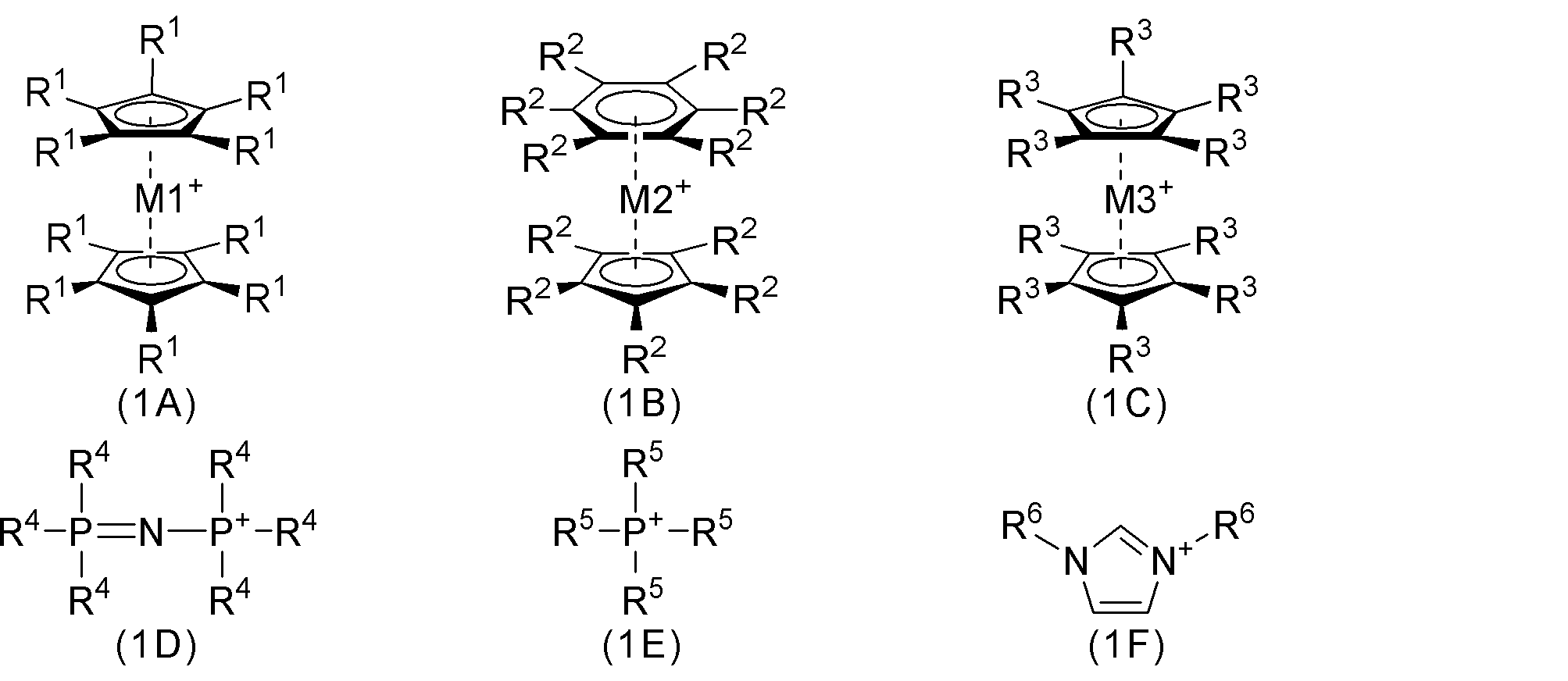
(式中、M1は、ロジウム又はイリジウムであり;M2は、ルテニウムであり;M3は、コバルトであり;R1~R6は、それぞれ独立して、水素原子、置換基を有していてもよいアルキル基、又は置換基を有していてもよいアリール基である。)
〔4〕
前記低分子疎水性イオンが、低分子疎水性アニオンであり、
前記低分子疎水性アニオンが、式(3F)~(3G)で表されるアニオンからなる群より選択される1種以上である、〔1〕又は〔2〕に記載の縦型ダイオード。
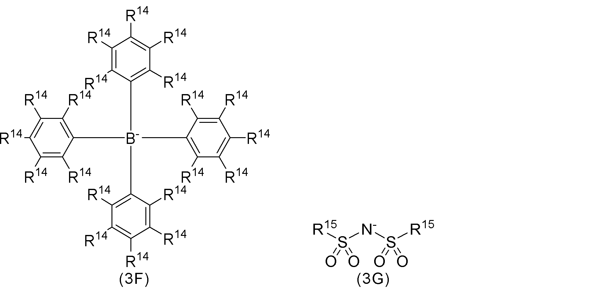
(式中、R14は、それぞれ独立して、水素原子、ハロゲン原子、又は置換基を有していてもよいフッ化アルキル基であり;R15は、それぞれ独立して、パーフルオロアルキル基であり、2つのR15は、互いに連結して環を形成していてもよい。)
〔5〕
前記低分子疎水性イオンが、前記第1電極の表面であって前記有機半導体層と隣接する面の10面積%以上50面積%以下に付着している、〔1〕~〔4〕のいずれかに記載の縦型ダイオード。
〔6〕
前記低分子疎水性イオンが、前記第1電極の表面であって前記有機半導体層と隣接する面の上でイオン層を形成しており、
前記イオン層の厚さが、2nm以下又は3分子層以下の厚さである、〔1〕~〔5〕のいずれかに記載の縦型ダイオード。
〔7〕
前記第1電極の表面であって前記有機半導体層と隣接する面に付着している前記低分子疎水性イオンのうち、対イオンと塩を形成している低分子疎水性イオンの割合が、25mol%以下であり、
前記対イオンが、前記有機半導体層を構成する有機半導体に由来するイオン、プロトン、水酸化物イオン、及び前記第1電極に含まれる金属のイオン以外の対イオンである、〔1〕~〔6〕のいずれかに記載の縦型ダイオード。
〔8〕
前記第1電極が、銅電極である、〔1〕~〔7〕のいずれかに記載の縦型ダイオード。
〔9〕
前記低分子疎水性イオンが、低分子疎水性カチオンであり、
前記有機半導体層が、ドープ層とアンドープ層とを有し、
前記ドープ層が、前記第2電極と隣接する層であり、かつ、ホール及びドーパントアニオンを含む、〔1〕~〔3〕及び〔5〕~〔8〕のいずれかに記載の縦型ダイオード。
〔10〕
前記低分子疎水性イオンが、低分子疎水性アニオンであり、
前記有機半導体層が、ドープ層とアンドープ層とを有し、
前記ドープ層が、前記第2電極と隣接する層であり、かつ、電子及びドーパントカチオンを含む、〔1〕~〔2〕及び〔4〕~〔8〕のいずれかに記載の縦型ダイオード。
〔11〕
前記有機半導体層の厚さが、15nm以上50nm以下である、〔1〕~〔10〕のいずれかに記載の縦型ダイオード。
〔12〕
周波数10MHzの交流電力から直流電力への変換効率が5%超である、〔1〕~〔11〕のいずれかに記載の縦型ダイオード。
〔13〕
周波数1GHzの交流電力から直流電力への変換効率が5%超である、〔1〕~〔12〕のいずれかに記載の縦型ダイオード。
〔14〕
第1電極、有機半導体層、及び第2電極がこの順に隣接して積層された縦型ダイオードの製造方法であって、
前記第1電極の表面と表面修飾液とを接触させることで、表面修飾された第1電極を得る電極修飾工程と、
前記電極修飾工程で修飾された前記第1電極の前記表面と前記有機半導体層とが接触するよう、前記第1電極と前記有機半導体層とを積層する積層工程とを含み、
前記表面修飾液が、下記表面修飾液(S1)~(S4)のいずれかである、縦型ダイオードの製造方法。
(S1)前記第1電極を還元するとともに低分子疎水性カチオンを生じる第1還元剤を含む表面修飾液。
(S2)前記第1電極を酸化するとともに低分子疎水性アニオンを生じる第1酸化剤を含む表面修飾液。
(S3)前記第1電極を還元する第2還元剤と低分子疎水性閉殻カチオンとを含む表面修飾液。
(S4)前記第1電極を酸化する第2酸化剤と低分子疎水性閉殻アニオンとを含む表面修飾液。
〔15〕
前記表面修飾液(S1)が、前記第1還元剤から生じる前記低分子疎水性カチオンとは異なる低分子疎水性カチオンをさらに含む、〔14〕に記載の縦型ダイオードの製造方法。
〔16〕
前記表面修飾液(S2)が、前記第1酸化剤から生じる前記低分子疎水性アニオンとは異なる低分子疎水性アニオンをさらに含む、〔14〕に記載の縦型ダイオードの製造方法。
〔17〕
前記表面修飾液が、前記表面修飾液(S1)又は前記表面修飾液(S2)である、〔14〕~〔16〕のいずれかに記載の縦型ダイオードの製造方法。
〔18〕
前記表面修飾液が、前記表面修飾液(S3)又は前記表面修飾液(S4)である、〔14〕に記載の縦型ダイオードの製造方法。
〔19〕
前記表面修飾液の溶媒が水であり、前記電極修飾工程が大気雰囲気下で行われる、〔14〕~〔18〕のいずれかに記載の縦型ダイオードの製造方法。
〔20〕
前記有機半導体層が、ドープ層とアンドープ層とを有する有機半導体層であり、かつ、前記ドープ層が前記第2電極に隣接する層であり、
第3酸化剤及び第3還元剤からなる群より選択される1種以上並びにドーパントイオンの塩を含む水溶液と、有機半導体層前駆体の表面とを接触させることで、前記ドープ層を形成するドーピング工程と、
前記有機半導体層と前記第2電極とを、前記ドープ層と前記第2電極とが接触するよう積層する積層工程と、
をさらに含む、〔14〕~〔19〕のいずれかに記載の縦型ダイオードの製造方法。
〔21〕
前記第3還元剤が、ヒドロキノン骨格を有するヒドロキノン化合物及び還元型補酵素からなる群より選択される1種以上であり、
前記第3酸化剤が、キノン骨格を有するキノン化合物である、〔20〕に記載の縦型ダイオードの製造方法。
〔22〕
電極の表面を修飾し、前記電極の仕事関数を変化させるための表面修飾液であって、
前記表面修飾液が、下記表面修飾液(S1)~(S4)のいずれかである、表面修飾液。
(S1)前記電極を還元するとともに低分子疎水性カチオンを生じる第1還元剤を含む表面修飾液。
(S2)前記電極を酸化するとともに低分子疎水性アニオンを生じる第1酸化剤を含む表面修飾液。
(S3)前記電極を還元する第2還元剤と低分子疎水性閉殻カチオンとを含む表面修飾液。
(S4)前記電極を酸化する第2酸化剤と低分子疎水性閉殻アニオンとを含む表面修飾液。
〔23〕
前記表面修飾液(S1)が、前記第1還元剤から生じる前記低分子疎水性カチオンとは異なる低分子疎水性カチオンをさらに含む、〔22〕に記載の表面修飾液。
〔24〕
前記表面修飾液(S2)が、前記第1酸化剤から生じる前記低分子疎水性アニオンとは異なる低分子疎水性アニオンをさらに含む、〔22〕に記載の表面修飾液。
〔25〕
前記表面修飾液が、前記表面修飾液(S1)又は前記表面修飾液(S2)である、〔22〕~〔24〕のいずれかに記載の表面修飾液。
〔26〕
前記表面修飾液が、前記表面修飾液(S3)又は前記表面修飾液(S4)である、〔22〕に記載の表面修飾液。
〔27〕
前記表面修飾液の溶媒が水である、〔22〕~〔26〕のいずれかに記載の表面修飾液。
〔28〕
第1電極、ドープ層とアンドープ層とを有する有機半導体層、及び第2電極がこの順に隣接して、かつ、前記ドープ層が前記第1電極又は前記第2電極に隣接して積層された縦型ダイオードであって、
前記ドープ層が、キャリア及びドーパントイオンを含み、
前記ドーパントイオンが、疎水性閉殻イオンである、縦型ダイオード。
〔29〕
前記ドープ層が、前記第2電極と隣接する層であり、
前記キャリアが、ホールであり、
前記ドーパントイオンが、疎水性閉殻アニオンであり、
前記第1電極の表面であって前記有機半導体層と隣接する面に低分子疎水性閉殻カチオンが付着している、〔28〕に記載の縦型ダイオード。
〔30〕
前記ドープ層が、前記第2電極と隣接する層であり、
前記キャリアが、電子であり、
前記ドーパントイオンが疎水性閉殻カチオンであり、
前記第1電極の表面であって前記有機半導体層と隣接する面に低分子疎水性閉殻アニオンが付着している、〔28〕に記載の縦型ダイオード。
〔31〕
前記ドープ層に含まれる前記ドーパントイオンのうち、対イオンと塩を形成している前記ドーパントイオンの割合が、25mol%以下であり、
前記対イオンが、前記有機半導体層を構成する有機半導体に由来するイオン、プロトン、水酸化物イオン、前記第1電極に含まれる金属のイオン、及び前記第2電極に含まれる金属のイオンである、〔28〕~〔30〕のいずれかに記載の縦型ダイオード。
〔32〕
前記ドープ層を構成する有機半導体が、前記アンドープ層を構成する有機半導体と同一の化合物である、〔28〕~〔31〕のいずれかに記載の縦型ダイオード。
〔33〕
前記有機半導体層の厚さが、15nm以上50nm以下である、〔28〕~〔32〕のいずれかに記載の縦型ダイオード。
〔34〕
第1電極、ドープ層とアンドープ層とを有する有機半導体層、及び第2電極がこの順に隣接して、かつ、前記ドープ層が前記第1電極又は前記第2電極に隣接して積層された縦型ダイオードの製造方法であって、
第4酸化剤又は第4還元剤及びドーパントイオンの塩を含む水溶液と、有機半導体層前駆体の表面とを接触させることで、前記ドープ層を形成するドーピング工程を含み、
記ドーパントイオンが、疎水性閉殻イオンである、縦型ダイオードの製造方法。
〔35〕
前記第4還元剤が、ヒドロキノン骨格を有するヒドロキノン化合物及び還元型補酵素からなる群より選択される1種以上であり、
前記第4酸化剤が、キノン骨格を有するキノン化合物である、〔34〕に記載の縦型ダイオードの製造方法。
〔36〕
前記ドープ層が、前記第2電極に隣接する層であり、
前記第1電極の表面と、表面修飾液とを接触させることで、第1電極の表面を修飾する電極修飾工程をさらに含み、
前記表面修飾液が、下記表面修飾液(S1)~(S4)のいずれかである、〔34〕又は〔35〕に記載の縦型ダイオードの製造方法。
(S1)前記第1電極を還元するとともに低分子疎水性カチオンを生じる第1還元剤を含む表面修飾液。
(S2)前記第1電極を酸化するとともに低分子疎水性アニオンを生じる第1酸化剤を含む表面修飾液。
(S3)前記第1電極を還元する第2還元剤と低分子疎水性閉殻カチオンとを含む表面修飾液。
(S4)前記第1電極を酸化する第2酸化剤と低分子疎水性閉殻アニオンとを含む表面修飾液。
〔37〕
前記表面修飾液が、前記表面修飾液(S1)又は前記表面修飾液(S2)である、〔36〕に記載の縦型ダイオードの製造方法。
〔38〕
前記表面修飾液が、前記表面修飾液(S3)又は前記表面修飾液(S4)である、〔36〕に記載の縦型ダイオードの製造方法。
〔39〕
前記表面修飾液の溶媒が水であり、前記電極修飾工程が大気雰囲気下で行われる、〔36〕~〔38〕のいずれかに記載の縦型ダイオードの製造方法。
第1電極、有機半導体層、及び第2電極がこの順に隣接して積層された縦型ダイオードであって、
前記第1電極の表面であって前記有機半導体層と隣接する面に低分子疎水性イオンが付着している、縦型ダイオード。
〔2〕
前記低分子疎水性イオンが、低分子疎水性閉殻イオンである、〔1〕に記載の縦型ダイオード。
〔3〕
前記低分子疎水性イオンが、低分子疎水性カチオンであり、
前記低分子疎水性カチオンが、式(1A)~(1F)で表されるカチオンからなる群より選択される1種以上である、〔1〕又は〔2〕に記載の縦型ダイオード。
(式中、M1は、ロジウム又はイリジウムであり;M2は、ルテニウムであり;M3は、コバルトであり;R1~R6は、それぞれ独立して、水素原子、置換基を有していてもよいアルキル基、又は置換基を有していてもよいアリール基である。)
〔4〕
前記低分子疎水性イオンが、低分子疎水性アニオンであり、
前記低分子疎水性アニオンが、式(3F)~(3G)で表されるアニオンからなる群より選択される1種以上である、〔1〕又は〔2〕に記載の縦型ダイオード。
(式中、R14は、それぞれ独立して、水素原子、ハロゲン原子、又は置換基を有していてもよいフッ化アルキル基であり;R15は、それぞれ独立して、パーフルオロアルキル基であり、2つのR15は、互いに連結して環を形成していてもよい。)
〔5〕
前記低分子疎水性イオンが、前記第1電極の表面であって前記有機半導体層と隣接する面の10面積%以上50面積%以下に付着している、〔1〕~〔4〕のいずれかに記載の縦型ダイオード。
〔6〕
前記低分子疎水性イオンが、前記第1電極の表面であって前記有機半導体層と隣接する面の上でイオン層を形成しており、
前記イオン層の厚さが、2nm以下又は3分子層以下の厚さである、〔1〕~〔5〕のいずれかに記載の縦型ダイオード。
〔7〕
前記第1電極の表面であって前記有機半導体層と隣接する面に付着している前記低分子疎水性イオンのうち、対イオンと塩を形成している低分子疎水性イオンの割合が、25mol%以下であり、
前記対イオンが、前記有機半導体層を構成する有機半導体に由来するイオン、プロトン、水酸化物イオン、及び前記第1電極に含まれる金属のイオン以外の対イオンである、〔1〕~〔6〕のいずれかに記載の縦型ダイオード。
〔8〕
前記第1電極が、銅電極である、〔1〕~〔7〕のいずれかに記載の縦型ダイオード。
〔9〕
前記低分子疎水性イオンが、低分子疎水性カチオンであり、
前記有機半導体層が、ドープ層とアンドープ層とを有し、
前記ドープ層が、前記第2電極と隣接する層であり、かつ、ホール及びドーパントアニオンを含む、〔1〕~〔3〕及び〔5〕~〔8〕のいずれかに記載の縦型ダイオード。
〔10〕
前記低分子疎水性イオンが、低分子疎水性アニオンであり、
前記有機半導体層が、ドープ層とアンドープ層とを有し、
前記ドープ層が、前記第2電極と隣接する層であり、かつ、電子及びドーパントカチオンを含む、〔1〕~〔2〕及び〔4〕~〔8〕のいずれかに記載の縦型ダイオード。
〔11〕
前記有機半導体層の厚さが、15nm以上50nm以下である、〔1〕~〔10〕のいずれかに記載の縦型ダイオード。
〔12〕
周波数10MHzの交流電力から直流電力への変換効率が5%超である、〔1〕~〔11〕のいずれかに記載の縦型ダイオード。
〔13〕
周波数1GHzの交流電力から直流電力への変換効率が5%超である、〔1〕~〔12〕のいずれかに記載の縦型ダイオード。
〔14〕
第1電極、有機半導体層、及び第2電極がこの順に隣接して積層された縦型ダイオードの製造方法であって、
前記第1電極の表面と表面修飾液とを接触させることで、表面修飾された第1電極を得る電極修飾工程と、
前記電極修飾工程で修飾された前記第1電極の前記表面と前記有機半導体層とが接触するよう、前記第1電極と前記有機半導体層とを積層する積層工程とを含み、
前記表面修飾液が、下記表面修飾液(S1)~(S4)のいずれかである、縦型ダイオードの製造方法。
(S1)前記第1電極を還元するとともに低分子疎水性カチオンを生じる第1還元剤を含む表面修飾液。
(S2)前記第1電極を酸化するとともに低分子疎水性アニオンを生じる第1酸化剤を含む表面修飾液。
(S3)前記第1電極を還元する第2還元剤と低分子疎水性閉殻カチオンとを含む表面修飾液。
(S4)前記第1電極を酸化する第2酸化剤と低分子疎水性閉殻アニオンとを含む表面修飾液。
〔15〕
前記表面修飾液(S1)が、前記第1還元剤から生じる前記低分子疎水性カチオンとは異なる低分子疎水性カチオンをさらに含む、〔14〕に記載の縦型ダイオードの製造方法。
〔16〕
前記表面修飾液(S2)が、前記第1酸化剤から生じる前記低分子疎水性アニオンとは異なる低分子疎水性アニオンをさらに含む、〔14〕に記載の縦型ダイオードの製造方法。
〔17〕
前記表面修飾液が、前記表面修飾液(S1)又は前記表面修飾液(S2)である、〔14〕~〔16〕のいずれかに記載の縦型ダイオードの製造方法。
〔18〕
前記表面修飾液が、前記表面修飾液(S3)又は前記表面修飾液(S4)である、〔14〕に記載の縦型ダイオードの製造方法。
〔19〕
前記表面修飾液の溶媒が水であり、前記電極修飾工程が大気雰囲気下で行われる、〔14〕~〔18〕のいずれかに記載の縦型ダイオードの製造方法。
〔20〕
前記有機半導体層が、ドープ層とアンドープ層とを有する有機半導体層であり、かつ、前記ドープ層が前記第2電極に隣接する層であり、
第3酸化剤及び第3還元剤からなる群より選択される1種以上並びにドーパントイオンの塩を含む水溶液と、有機半導体層前駆体の表面とを接触させることで、前記ドープ層を形成するドーピング工程と、
前記有機半導体層と前記第2電極とを、前記ドープ層と前記第2電極とが接触するよう積層する積層工程と、
をさらに含む、〔14〕~〔19〕のいずれかに記載の縦型ダイオードの製造方法。
〔21〕
前記第3還元剤が、ヒドロキノン骨格を有するヒドロキノン化合物及び還元型補酵素からなる群より選択される1種以上であり、
前記第3酸化剤が、キノン骨格を有するキノン化合物である、〔20〕に記載の縦型ダイオードの製造方法。
〔22〕
電極の表面を修飾し、前記電極の仕事関数を変化させるための表面修飾液であって、
前記表面修飾液が、下記表面修飾液(S1)~(S4)のいずれかである、表面修飾液。
(S1)前記電極を還元するとともに低分子疎水性カチオンを生じる第1還元剤を含む表面修飾液。
(S2)前記電極を酸化するとともに低分子疎水性アニオンを生じる第1酸化剤を含む表面修飾液。
(S3)前記電極を還元する第2還元剤と低分子疎水性閉殻カチオンとを含む表面修飾液。
(S4)前記電極を酸化する第2酸化剤と低分子疎水性閉殻アニオンとを含む表面修飾液。
〔23〕
前記表面修飾液(S1)が、前記第1還元剤から生じる前記低分子疎水性カチオンとは異なる低分子疎水性カチオンをさらに含む、〔22〕に記載の表面修飾液。
〔24〕
前記表面修飾液(S2)が、前記第1酸化剤から生じる前記低分子疎水性アニオンとは異なる低分子疎水性アニオンをさらに含む、〔22〕に記載の表面修飾液。
〔25〕
前記表面修飾液が、前記表面修飾液(S1)又は前記表面修飾液(S2)である、〔22〕~〔24〕のいずれかに記載の表面修飾液。
〔26〕
前記表面修飾液が、前記表面修飾液(S3)又は前記表面修飾液(S4)である、〔22〕に記載の表面修飾液。
〔27〕
前記表面修飾液の溶媒が水である、〔22〕~〔26〕のいずれかに記載の表面修飾液。
〔28〕
第1電極、ドープ層とアンドープ層とを有する有機半導体層、及び第2電極がこの順に隣接して、かつ、前記ドープ層が前記第1電極又は前記第2電極に隣接して積層された縦型ダイオードであって、
前記ドープ層が、キャリア及びドーパントイオンを含み、
前記ドーパントイオンが、疎水性閉殻イオンである、縦型ダイオード。
〔29〕
前記ドープ層が、前記第2電極と隣接する層であり、
前記キャリアが、ホールであり、
前記ドーパントイオンが、疎水性閉殻アニオンであり、
前記第1電極の表面であって前記有機半導体層と隣接する面に低分子疎水性閉殻カチオンが付着している、〔28〕に記載の縦型ダイオード。
〔30〕
前記ドープ層が、前記第2電極と隣接する層であり、
前記キャリアが、電子であり、
前記ドーパントイオンが疎水性閉殻カチオンであり、
前記第1電極の表面であって前記有機半導体層と隣接する面に低分子疎水性閉殻アニオンが付着している、〔28〕に記載の縦型ダイオード。
〔31〕
前記ドープ層に含まれる前記ドーパントイオンのうち、対イオンと塩を形成している前記ドーパントイオンの割合が、25mol%以下であり、
前記対イオンが、前記有機半導体層を構成する有機半導体に由来するイオン、プロトン、水酸化物イオン、前記第1電極に含まれる金属のイオン、及び前記第2電極に含まれる金属のイオンである、〔28〕~〔30〕のいずれかに記載の縦型ダイオード。
〔32〕
前記ドープ層を構成する有機半導体が、前記アンドープ層を構成する有機半導体と同一の化合物である、〔28〕~〔31〕のいずれかに記載の縦型ダイオード。
〔33〕
前記有機半導体層の厚さが、15nm以上50nm以下である、〔28〕~〔32〕のいずれかに記載の縦型ダイオード。
〔34〕
第1電極、ドープ層とアンドープ層とを有する有機半導体層、及び第2電極がこの順に隣接して、かつ、前記ドープ層が前記第1電極又は前記第2電極に隣接して積層された縦型ダイオードの製造方法であって、
第4酸化剤又は第4還元剤及びドーパントイオンの塩を含む水溶液と、有機半導体層前駆体の表面とを接触させることで、前記ドープ層を形成するドーピング工程を含み、
記ドーパントイオンが、疎水性閉殻イオンである、縦型ダイオードの製造方法。
〔35〕
前記第4還元剤が、ヒドロキノン骨格を有するヒドロキノン化合物及び還元型補酵素からなる群より選択される1種以上であり、
前記第4酸化剤が、キノン骨格を有するキノン化合物である、〔34〕に記載の縦型ダイオードの製造方法。
〔36〕
前記ドープ層が、前記第2電極に隣接する層であり、
前記第1電極の表面と、表面修飾液とを接触させることで、第1電極の表面を修飾する電極修飾工程をさらに含み、
前記表面修飾液が、下記表面修飾液(S1)~(S4)のいずれかである、〔34〕又は〔35〕に記載の縦型ダイオードの製造方法。
(S1)前記第1電極を還元するとともに低分子疎水性カチオンを生じる第1還元剤を含む表面修飾液。
(S2)前記第1電極を酸化するとともに低分子疎水性アニオンを生じる第1酸化剤を含む表面修飾液。
(S3)前記第1電極を還元する第2還元剤と低分子疎水性閉殻カチオンとを含む表面修飾液。
(S4)前記第1電極を酸化する第2酸化剤と低分子疎水性閉殻アニオンとを含む表面修飾液。
〔37〕
前記表面修飾液が、前記表面修飾液(S1)又は前記表面修飾液(S2)である、〔36〕に記載の縦型ダイオードの製造方法。
〔38〕
前記表面修飾液が、前記表面修飾液(S3)又は前記表面修飾液(S4)である、〔36〕に記載の縦型ダイオードの製造方法。
〔39〕
前記表面修飾液の溶媒が水であり、前記電極修飾工程が大気雰囲気下で行われる、〔36〕~〔38〕のいずれかに記載の縦型ダイオードの製造方法。
本開示によれば、整流特性に優れた縦型ダイオードを提供できるという効果を奏し得る。そして、本開示の課題及び効果は、具体的に上記に記載したものに限らず、明細書全体より当業者に明らかにされるものを含む。
以下に、本開示について具体的な実施形態を挙げて説明するが、各実施形態における各構成及びそれらの組み合わせ等は、一例であって、本開示の主旨から逸脱しない範囲内で、適宜、構成の付加、省略、置換、及びその他の変更が可能である。本開示は、実施形態によって限定されるものではない。
また、本明細書に開示される各々の態様は、本明細書に開示される他のいかなる特徴とも組み合わせることができる。
また、本明細書に開示される各々の態様は、本明細書に開示される他のいかなる特徴とも組み合わせることができる。
本明細書において、範囲を示す「X~Y」は「X以上Y以下」を意味する。また、「X~Y」又は「X以上Y以下」で表される数値範囲が段階的(例えば、好ましい順)に記載されている場合、各数値範囲の上限及び下限は任意に組み合わせることができる。
また、本開示において、「x1、x2、及びx3等のX」のような記載は、Xの一例としてx1、x2、及びx3等を挙げたものであって、Xがx1、x2、及びx3等に限られることを意味するものではない。
また、本開示において、「x1、x2、及びx3等のX」のような記載は、Xの一例としてx1、x2、及びx3等を挙げたものであって、Xがx1、x2、及びx3等に限られることを意味するものではない。
〔1.縦型ダイオードの製造方法〕
本開示の第1実施形態は、第1電極、有機半導体層、及び第2電極がこの順に隣接して積層された縦型ダイオードの製造方法である。本実施形態に係る製造方法は、第1電極の表面と、表面修飾液とを接触させることで、表面修飾された第1電極を得る電極修飾工程;及び前記電極修飾工程で修飾された前記第1電極の前記表面と前記有機半導体層とが接触するよう、前記第1電極と前記有機半導体層とを積層する積層工程;を含む。また、電極修飾工程で用いる表面修飾液は、表面修飾液(S1)~表面修飾液(S4)のいずれかである。
(S1)第1電極を還元するとともに低分子疎水性カチオンを生じる第1還元剤を含む表面修飾液。
(S2)第1電極を酸化するとともに低分子疎水性アニオンを生じる第1酸化剤を含む表面修飾液。
(S3)第1電極を還元する第2還元剤と低分子疎水性閉殻カチオンとを含む表面修飾液。
(S4)第1電極を酸化する第2酸化剤と低分子疎水性閉殻アニオンとを含む表面修飾液。
本開示の第1実施形態は、第1電極、有機半導体層、及び第2電極がこの順に隣接して積層された縦型ダイオードの製造方法である。本実施形態に係る製造方法は、第1電極の表面と、表面修飾液とを接触させることで、表面修飾された第1電極を得る電極修飾工程;及び前記電極修飾工程で修飾された前記第1電極の前記表面と前記有機半導体層とが接触するよう、前記第1電極と前記有機半導体層とを積層する積層工程;を含む。また、電極修飾工程で用いる表面修飾液は、表面修飾液(S1)~表面修飾液(S4)のいずれかである。
(S1)第1電極を還元するとともに低分子疎水性カチオンを生じる第1還元剤を含む表面修飾液。
(S2)第1電極を酸化するとともに低分子疎水性アニオンを生じる第1酸化剤を含む表面修飾液。
(S3)第1電極を還元する第2還元剤と低分子疎水性閉殻カチオンとを含む表面修飾液。
(S4)第1電極を酸化する第2酸化剤と低分子疎水性閉殻アニオンとを含む表面修飾液。
本開示において、「疎水性」とは、水に対する親和力が低く、水に溶解及び混合しない又はしにくい性質を意味する。
本開示において、「疎水性」のイオン(カチオン又はアニオン)とは、それぞれ、1以上の疎水性部位を含むイオンを意味する。疎水性部位としては、例えば、シクロペンタジエニル基及びフェニル基等の炭素数5以上20以下の芳香族炭化水素基;イミダゾリル基等の炭素数3以上20以下の芳香族複素環基;オクチル基等の炭素数8以上20以下の炭化水素基;トリフルオロメチル及びペンタフルオロエチル基等の炭素数1以上20以下のフッ化脂肪族炭化水素基、好ましくはパーフルオロ脂肪族炭化水素基;並びにペンタフルオロフェニル基及びヘプタフルオロナフチル基等の炭素数6以上20以下のフッ化芳香族炭化水素基、好ましくはパーフルオロ芳香族炭化水素基;等が好ましく挙げられる。疎水性イオンの1分子あたりの疎水性部位の数は、好ましくは1以上10以下、より好ましくは1以上8以下、さらに好ましくは2以上6以下、特に好ましくは2以上4以下である。疎水性部位の数が上記下限以上であることにより、イオンが十分嵩高くなり、疎水性が発揮されるため、水及び大気に対する安定性の高い表面修飾電極が得られる。また、疎水性部位の数が上記上限以下であることにより、疎水性イオンを十分な濃度で含む表面修飾液を調製することができる。
疎水性イオンは、電荷が疎水性イオン内に広く非局在化しているものが望ましい。電荷の非局在化により、局所的な水との相互作用を抑制することが可能であり、疎水性イオンの疎水性が向上するためである。電荷を疎水性イオンの広い範囲に非局在化するためには、疎水性イオンに共役構造、電子求引基(疎水性イオンが疎水性アニオンである場合)、電子供与基(疎水性イオンが疎水性カチオンである場合)等を持たせることが好適である。
本開示において、「低分子」とは、分子量分布を有さず、かつ、分子量が2,000以下、好ましくは1,000以下、より好ましくは800以下、さらに好ましくは500以下であることを意味する。これに対し、分子量分布を有し、かつ、分子量が1,000以上の分子又はイオンを「高分子」又は「ポリマー」などと呼び区別する。
本実施形態によれば、優れた整流特性を示す縦型ダイオードを得ることができる。したがって、本実施形態に係る製造方法は、整流ダイオードを製造する方法として有用である。整流ダイオードは順方向において逆方向と比較して電流値が高く、その比率である整流比が2桁以上、好ましくは3桁以上である特徴を有する。また、後述するように、第1電極の仕事関数を大きく変化させることが可能であるため、電極材料選択の自由度を大きく向上することができる。さらに、本実施形態の好適な態様によれば、高周波応答性に優れた縦型ダイオード又は低電圧でも高い電流密度を示す縦型ダイオードを得ることができる。なお、本開示において、「電流密度」は、順方向の電流密度を意味するものとする。また、「低電圧で高い電流密度」とは、順方向電圧2Vのときの順方向の電流密度が1Acm-2以上、好ましくは10Acm-2以上、より好ましくは100Acm-2以上であることを意味する。
本実施形態に係る製造方法により得られる縦型ダイオードは、太陽電池及び発光ダイオード等のダイオード構造を有する種々のデバイスに適用し得ると考えられ、また、高周波応答性を要する無線通信用電子タグ等への展開も期待される。
本実施形態に係る製造方法により得られる縦型ダイオードは、太陽電池及び発光ダイオード等のダイオード構造を有する種々のデバイスに適用し得ると考えられ、また、高周波応答性を要する無線通信用電子タグ等への展開も期待される。
〔1-1.電極修飾工程〕
電極修飾工程は、第1電極の表面と表面修飾液(S1)~(S4)のいずれかとを接触させることにより、第1電極の表面を修飾する工程である。
電極修飾工程は、第1電極の表面と表面修飾液(S1)~(S4)のいずれかとを接触させることにより、第1電極の表面を修飾する工程である。
本工程により、表面修飾された第1電極(以下、「表面修飾電極」と称することがある。)が得られる。表面修飾された第1電極は、第1電極の表面であって縦型ダイオードを作製した際に有機半導体層と隣接する面に低分子疎水性イオンが付着したものである。
電極修飾工程では、第1電極の表面と表面修飾液とを接触させるという簡易な溶液プロセスにより、第1電極の仕事関数を大きくシフトさせることができる。加えて、ポリマー堆積等の表面修飾により電極の仕事関数を変化させる従来技術では、得られる電極の大気安定性が低く、大気に曝露されると仕事関数が表面修飾前と同等程度に戻るという問題があるが、本実施形態における電極修飾工程によれば、耐水性及び大気安定性の高い表面修飾電極を得ることができる。したがって、後述する実施例に示されるように、表面修飾電極を大気に曝露した後に仕事関数を測定した場合であっても、電極修飾工程で浅く又は深くシフトした仕事関数を維持される。
ここで、仕事関数とは、フェルミ準位と真空準位の差(正の値)である。フェルミ準位とは、電子の占有確立が0.5となるエネルギー準位である。金属において、仕事関数は、1個の電子を真空中に取り出すのに必要な最小エネルギーであるイオン化ポテンシャルに等しい。
仕事関数は、紫外光電子分光装置を用いて測定することができる。ただし、測定対象が金属である場合には、仕事関数は、イオン化ポテンシャル測定を実施するための光電子収量分光法装置(例えば、理研計器株式会社製「AC-3」)により測定された値であるものとする。
仕事関数は、紫外光電子分光装置を用いて測定することができる。ただし、測定対象が金属である場合には、仕事関数は、イオン化ポテンシャル測定を実施するための光電子収量分光法装置(例えば、理研計器株式会社製「AC-3」)により測定された値であるものとする。
〔1-1-1.表面修飾液〕
第1電極の表面を修飾するための表面修飾液(S1)~(S4)は、好ましくは溶液又は分散液であり、より好ましくは溶液である。以下、表面修飾液(S1)~(S4)に含まれる成分について説明する。
第1電極の表面を修飾するための表面修飾液(S1)~(S4)は、好ましくは溶液又は分散液であり、より好ましくは溶液である。以下、表面修飾液(S1)~(S4)に含まれる成分について説明する。
(表面修飾液(S1))
表面修飾液(S1)に含まれる第1還元剤は、第1電極を還元するとともに低分子疎水性カチオンを生じる化合物である。表面修飾液として表面修飾液(S1)を使用する場合、本工程では、第1電極に電子が注入されることにより(すなわち、第1電極の表面が還元されることにより)、第1電極の表面が負に帯電する。そして、この負に帯電した第1電極の表面に第1還元剤から生じた低分子疎水性カチオンが静電的に付着し、表面が修飾された第1電極が得られる。このとき、低分子疎水性カチオンは、第1電極に静電的に付着して、カチオン層を形成する。カチオン層の厚さは、3分子層以下あることが好ましく、2分子層以下であることがより好ましく、単分子層以下であることがさらに好ましい。具体的な厚さで表すと、カチオン層の厚さは、2nm以下であることが好ましく、1nm以下であることがより好ましい。カチオン層の厚さは、X線光電子分光法(XPS)分析により求めることができる。なお、低分子疎水性カチオンを生じる第1還元剤もまた、低分子化合物である。
表面修飾液(S1)に含まれる第1還元剤は、第1電極を還元するとともに低分子疎水性カチオンを生じる化合物である。表面修飾液として表面修飾液(S1)を使用する場合、本工程では、第1電極に電子が注入されることにより(すなわち、第1電極の表面が還元されることにより)、第1電極の表面が負に帯電する。そして、この負に帯電した第1電極の表面に第1還元剤から生じた低分子疎水性カチオンが静電的に付着し、表面が修飾された第1電極が得られる。このとき、低分子疎水性カチオンは、第1電極に静電的に付着して、カチオン層を形成する。カチオン層の厚さは、3分子層以下あることが好ましく、2分子層以下であることがより好ましく、単分子層以下であることがさらに好ましい。具体的な厚さで表すと、カチオン層の厚さは、2nm以下であることが好ましく、1nm以下であることがより好ましい。カチオン層の厚さは、X線光電子分光法(XPS)分析により求めることができる。なお、低分子疎水性カチオンを生じる第1還元剤もまた、低分子化合物である。
表面修飾液(S1)は、第1還元剤から生じる低分子疎水性カチオンとは異なる低分子疎水性カチオン(以下、「他の低分子疎水性カチオン」と称することがある。)をさらに含むことが好ましい。表面修飾液(S1)が他の低分子疎水性カチオンをさらに含む場合、還元により負に帯電した第1電極に他の低分子疎水性カチオンが静電的に付着したり、第1電極に静電的に付着した第1還元剤由来の低分子疎水性カチオンが他の低分子疎水性カチオンで置き換わったりする。そのため、第1電極の表面には、第1還元剤由来の低分子疎水性カチオン及び他の低分子疎水性カチオン、又は他の低分子疎水性カチオンによりカチオン層が形成される。カチオン層中の第1還元剤由来の低分子疎水性カチオンと他の低分子疎水性カチオンとのモル比は、表面修飾液(S1)中の他の低分子疎水性カチオンの濃度や疎水性の程度を調整することで調整できる。
したがって、第1還元剤から生じる低分子疎水性カチオンの安定性が不十分である場合、及び第1還元剤が高価である場合等には、表面修飾液(S1)に他の低分子疎水性カチオンを含有させることにより、より大気及び水に対して安定な表面修飾電極をより低コストで作製することが可能となる。
以下、第1還元剤由来の低分子疎水性カチオンと他の低分子疎水性カチオンとを総称して「低分子疎水性カチオン」、「低分子疎水性イオン」などと称することがある。
第1電極の表面が上記のように修飾されると、第1電極の表面と低分子疎水性カチオンとの界面に大きなダイポールが形成され、その結果、第1電極の仕事関数が、修飾前よりも浅く(小さく)なる。本実施形態における電極修飾工程による第1電極の仕事関数のシフト幅は、非常に大きいものであり、例えば、後述する実施例に示されるように、金電極の仕事関数は、表面修飾により、約5.0eVから約3.7eVにシフトする。
第1電極の仕事関数が小さくなることにより、第1電極から有機半導体層への電子注入性は、大きく向上する。これにより、電子は、第1電極から有機半導体のLUMOに容易に入ることができるようになるため、第1電極から有機半導体層を通って第2電極へと電子が容易に移動できるようになる。一方、第2電極から有機半導体層への電子注入性はほとんど変化せず、第2電極から第1電極への電子の移動は、第1電極から第2電極への電子の移動に比べて困難となる。換言すると、第1電極の表面修飾により、第2電極から第1電極へ電流が流れ易くなり、第1電極から第2電極への電流の流れ易さはほとんど変化せず、したがって、縦型ダイオードの整流特性が向上し、ひいては縦型ダイオードの安定動作を実現し得る。また、縦型ダイオードの低電圧における電流密度を高めることも可能となる。
以上より、第1還元剤を含む表面修飾液(S1)を用いて第1電極を修飾する場合、有機半導体層として電子輸送性有機半導体の層、すなわち、n型有機半導体の層を用い、第1電極を電子注入電極(カソード(陰極))とすることにより、整流特性に優れた縦型ダイオードを得ることができる。また、低電圧でも高い電流密度を示す縦型ダイオードを得ることができる。このとき、有機半導体層全体がn型有機半導体の層である必要はなく、例えば、有機半導体層が多層構造を有する場合は、第1電極と隣接する層のみがn型有機半導体の層であれば、同様に上記効果が得られる。
ここで、従来技術として、電極にポリマーや塩を堆積させることにより、電極の仕事関数を調整する方法が知られている。しかしながら、ポリマーを堆積する方法では、電極と有機半導体層との間に厚さが単分子層よりも厚いポリマーの層が形成され、電極から有機半導体層への電子注入性が著しく低下するという不具合が生じる。塩を堆積する方法では、電極に堆積させる塩として、カチオン種とハロゲン化物イオン等の対アニオンとの塩が用いられている。この塩は、電極から有機半導体層への電子注入性を低下させるだけでなく、ハロゲン化物イオン等が有機半導体層等に拡散してデバイスの寿命を低下させるという問題もある。また、ポリマー及び塩は、いずれも、これらの材料を薄く堆積した場合であっても、材料に仕事関数制御を担う部位以外を含むため、電子注入を妨げる余剰な働きが生じることは避けられない。
また、他の従来技術として、自己組織化単分子膜を金属と共有結合することにより、単分子膜のダイポールを用いて仕事関数を制御する手法が知られている。このような手法では清浄な金属表面において、金属種に適した反応を示す分子材料を用いることが必要である。実際の半導体デバイス製造工程において清浄表面を用いることは他のリソグラフィーをはじめとする工程を踏まえると困難である場合が多い。また、金属種に限定が生じる。さらに、自己組織化単分子膜材料の形成する結合は強固でない場合も多く、熱による脱離が生じる場合もある。一方で本技術では酸化還元反応を用いているため、表面の清浄度や金属・導電性材料種類に原理的に依存せずに処理を実施可能である。このため、本実施形態に係る製造方法は、半導体素子製造において原理的に優位性を有する。
本実施形態は、還元反応によって負に帯電した第1電極の表面に低分子疎水性カチオンが付着(吸着)して薄いカチオン層が形成されるものであるため、第1電極と有機半導体層との間に電子移動を阻害するほどの余剰の層が形成されたり、塩が形成したりする問題が効果的に抑制される。そのため、第1電極と有機半導体層との間の優れた電子移動性、縦型ダイオードの整流特性に加え、縦型ダイオードの長寿命化及び低電圧における電流密度の向上も実現し得る。
第1還元剤としては、電子と低分子疎水性カチオンとを生じ、第1電極を還元できる限り特に限定されない。
第1還元剤から生じる低分子疎水性カチオンは、疎水性が高く、かつ、大気及び水に対して安定な低分子疎水性カチオンであることが好ましく、低分子疎水性閉殻カチオンであることがより好ましい。低分子疎水性閉殻カチオンは、溶媒中、特に水中での安定性が高いからである。
第1還元剤から生じる低分子疎水性カチオンとしては、式(1A)~(1C)で表される低分子疎水性閉殻カチオンが好ましく挙げられる。第1還元剤から生じる低分子疎水性カチオンは、式(1A)~(1B)で表されるカチオンから選択される1種以上であることが好ましく、大気及び水に対する安定性がより高い点で、式(1B)で表されるカチオンから選択される1種以上であることがより好ましい。
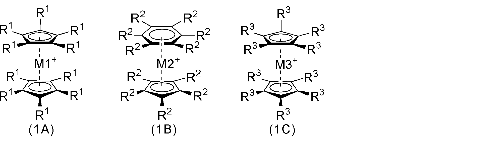
式中、M1は、ロジウム又はイリジウムであり、好ましくはロジウムである。
式中、M2は、ルテニウムである。
式中、M3は、コバルトである。
式中、R1~R3は、それぞれ独立して、水素原子、置換基を有していてもよいアルキル基、又は置換基を有していてもよいアリール基である。
R1は、好ましくは水素原子又は置換基を有していてもよいアルキル基であり、より好ましくは水素原子又は無置換のアルキル基である。
R2は、好ましくは水素原子又は置換基を有していてもよいアルキル基であり、より好ましくは水素原子又は無置換のアルキル基である。
R3は、好ましくは水素原子又は置換基を有していてもよいアルキル基であり、より好ましくは水素原子又は無置換のアルキル基である。
R2は、好ましくは水素原子又は置換基を有していてもよいアルキル基であり、より好ましくは水素原子又は無置換のアルキル基である。
R3は、好ましくは水素原子又は置換基を有していてもよいアルキル基であり、より好ましくは水素原子又は無置換のアルキル基である。
R1~R3で表されるアルキル基及びアリール基が有していてもよい置換基としては、重水素原子;ヒドロキシ基;フッ素原子、塩素原子、及び臭素原子等のハロゲン原子;メチル基、エチル基、n-プロピル基、及びイソプロピル基等の炭素数1以上4以下のアルキル基;シクロプロピル基及びシクロブチル基等のシクロアルキル基;フェニル基、1-ナフチル基、及び2-ナフチル基等の炭素数6以上12以下のアリール基;並びにベンジル基及び2-フェニルエチル基等のアラルキル基;等が挙げられるが、これらに限定されるものではない。
R1~R3で表される置換基を有していてもよいアルキル基の炭素数は、特に限定されないが、好ましくは1以上20以下、より好ましくは1以上12以下、さらに好ましくは2以上8以下、特に好ましくは2以上6以下である。
R1~R3で表される置換基を有していてもよいアルキル基の具体例としては、メチル基、エチル基、n-プロピル基、イソプロピル基、n-ブチル基、sec-ブチル基、tert-ブチル基、イソブチル基、n-ペンチル基、イソペンチル基、ネオペンチル基、n-ヘキシル基、トリフルオロメチル基、ペンタフルオロエチル基、ヒドロキシメチル基、及び2-ヒドロキシエチル基等が挙げられ、好ましくはメチル基である。
R1~R3で表される置換基を有していてもよいアリール基の炭素数は、特に限定されないが、好ましくは6以上20以下、より好ましくは6以上14以下である。
R1~R3で表される置換基を有していてもよいアリール基の具体例としては、フェニル基、1-ナフチル基、2-ナフチル基、9-フェナントレニル基、9-フルオレニル基、o-トリル基、m-トリル基、p-トリル基、メシチル基、ペンタフルオロフェニル基、及びp-トリフルオロメチル基等が挙げられ、好ましくはフェニル基又はメシチル基である。
式(1A)で表される低分子疎水性閉殻カチオンの具体例としては、下記カチオンが好ましく挙げられる。

式(1B)で表される低分子疎水性閉殻カチオンの具体例としては、下記カチオンが好ましく挙げられる。
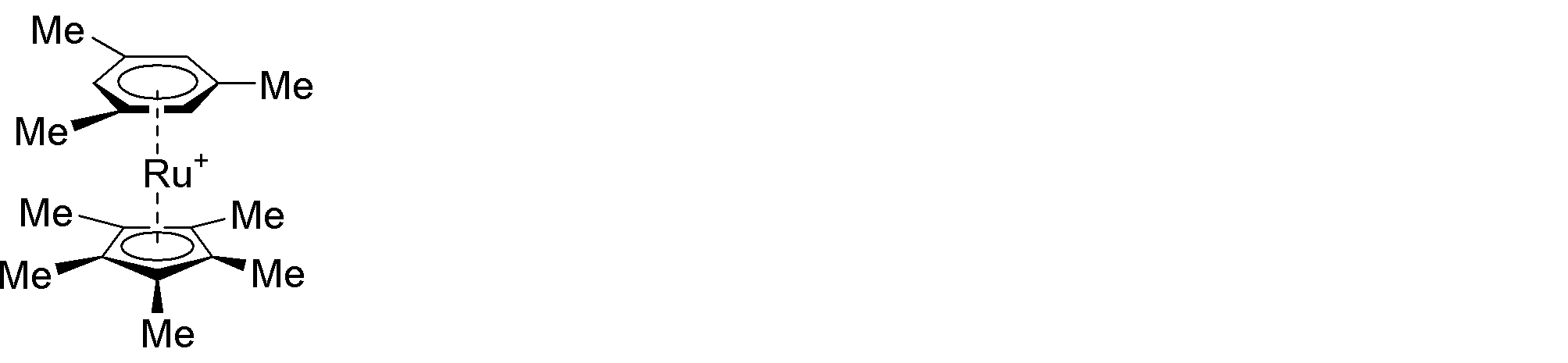
式(1C)で表される低分子疎水性閉殻カチオンの具体例としては、下記カチオンが好ましく挙げられる。
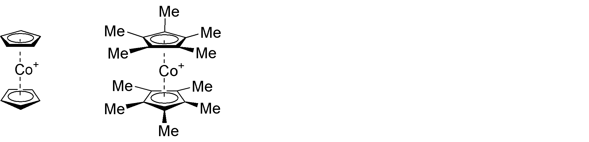
これらの低分子疎水性カチオンを生じる1還元剤としては、式(2A)~(2C)で表される化合物が挙げられる。式(2A)~(2C)で表される化合物は、それぞれ、式(1A)~(1C)で表される低分子疎水性閉殻カチオンを生じる第1還元剤である。したがって、これらのうち、第1還元剤は、式(2A)~(2B)で表される化合物から選択される1種以上であることが好ましく、大気及び水に対する安定性がより高い低分子疎水性閉殻カチオンを生じ得る点で、式(2B)で表される化合物から選択される1種以上であることがより好ましい。
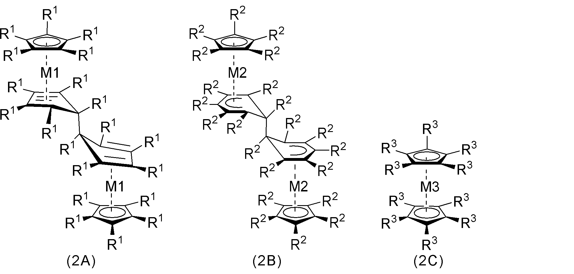
式(2A)中のM1及びR1は、それぞれ、式(1A)中のM1及びR1と同義であり、その好ましい態様も同様である。
式(2B)中のM2及びR2は、それぞれ、式(1B)中のM2及びR2と同義であり、その好ましい態様も同様である。
式(2C)中のM3及びR3は、それぞれ、式(1C)中のM3及びR3と同義であり、その好ましい態様も同様である。
式(2B)中のM2及びR2は、それぞれ、式(1B)中のM2及びR2と同義であり、その好ましい態様も同様である。
式(2C)中のM3及びR3は、それぞれ、式(1C)中のM3及びR3と同義であり、その好ましい態様も同様である。
式(2A)で表される化合物の具体例としては、下記化合物が好ましく挙げられる。
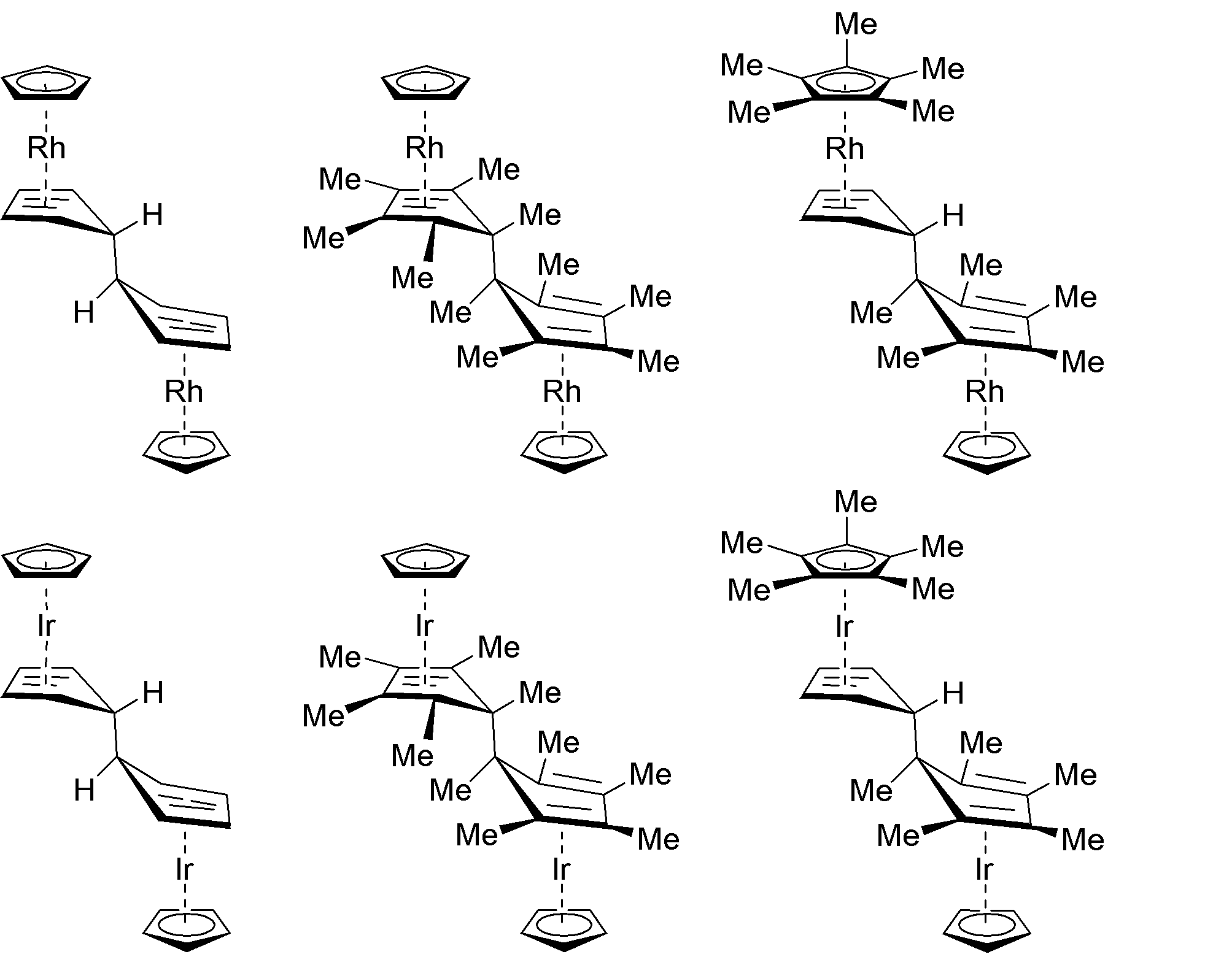
式(2B)で表される化合物の具体例としては、下記化合物が好ましく挙げられる。
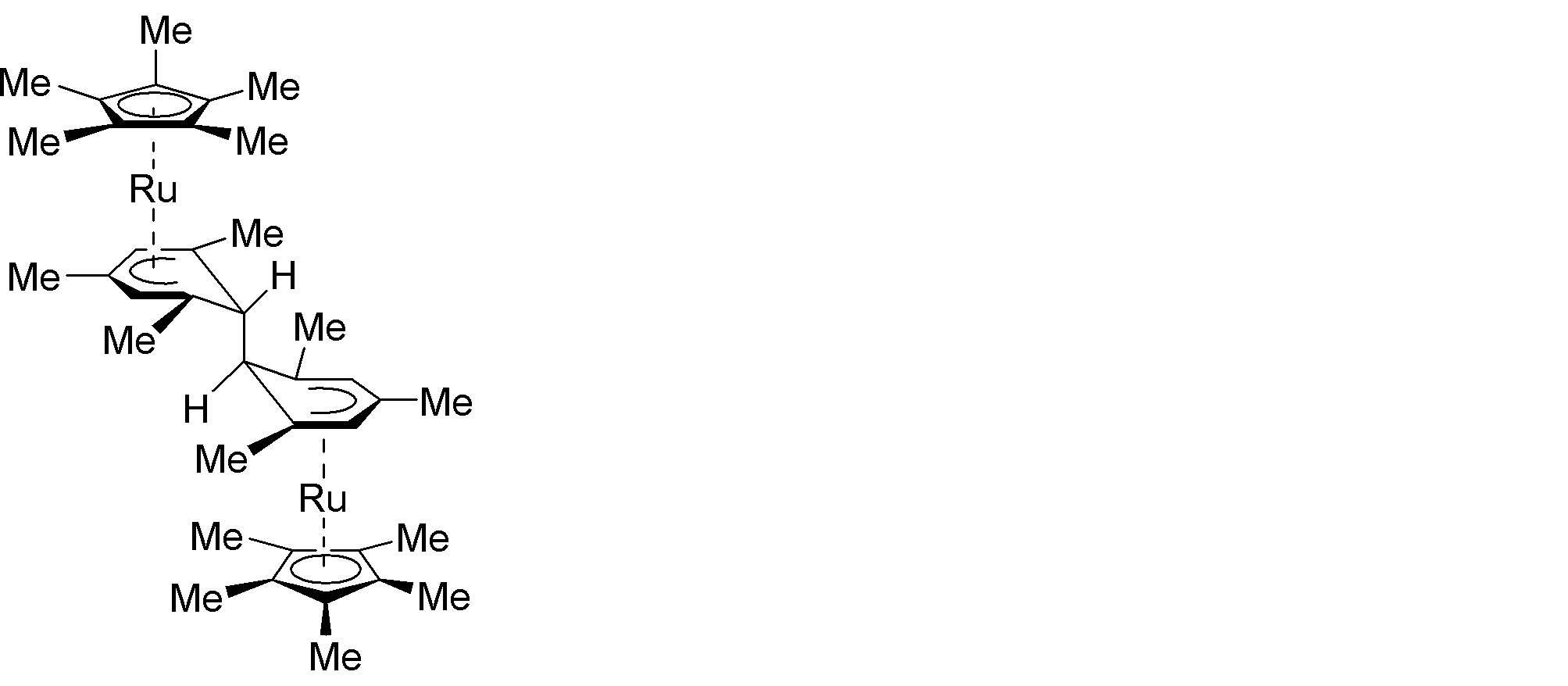
式(2C)で表される化合物の具体例としては、コバルトセン及びデカメチルコバルトセン等が好ましく挙げられる。
第1還元剤は、1種単独で使用してもよく、2種以上を任意の比率及び組み合わせで併用してもよい。したがって、第1電極の表面に付着する低分子疎水性カチオンもまた、1種単独又は2種以上であってよい。
表面修飾液(S1)に含まれる他の低分子疎水性カチオンとしては、第1還元剤から生じる低分子疎水性カチオンと同義であり、その好ましい態様も同様である。低分子疎水性カチオンは、1種単独で使用してもよく、2種以上を任意の比率及び組み合わせで併用してもよい。ただし、一の表面修飾液(S1)に含まれる他の低分子疎水性カチオンは、第1還元剤由来の低分子疎水性カチオンとは異なるカチオンである。
表面修飾液(S1)に含まれる他の低分子疎水性カチオンの対アニオンとしては、特に限定されないが、例えば水酸化物イオン;塩化物イオン、臭化物イオン、ヨウ化物イオン等のハロゲン化物イオン;炭酸イオン;硫酸イオン;並びにリン酸イオン;等が挙げられる。これらのうち、対アニオンは、第1電極から有機半導体層への電子注入を阻害するハロゲン化物塩の堆積を抑制できる点で、水酸化物イオンであることが好ましい。
表面修飾液(S1)中の第1還元剤の総濃度は、特に限定されず、第1還元剤の種類、後述する低分子疎水性イオン被覆率、及び仕事関数のシフト幅等に応じて適宜選択すればよい。例えば、第1還元剤の総濃度は、好ましくは0.01質量%以上3.00質量%以下、より好ましくは0.10質量%以上1.00質量%以下である。
表面修飾液(S1)が他の低分子疎水性カチオンを含む場合、表面修飾液(S1)中の他の低分子疎水性カチオンの総濃度は、特に限定されず、他の低分子疎水性カチオンの種類、後述する低分子疎水性イオン被覆率、仕事関数のシフト幅、及び第1電極を修飾する全低分子疎水性カチオン中の他の低分子疎水性カチオンの割合等に応じて適宜選択すればよい。例えば、低分子疎水性カチオンの総濃度は、好ましくは0.01質量%以上3.00質量%以下、より好ましくは0.10質量%以上1.00質量%以下である。
(表面修飾液(S2))
表面修飾液(S2)に含まれる第1酸化剤は、第1電極を酸化するとともに低分子疎水性アニオンを生じる化合物である。表面修飾液として表面修飾液(S2)を使用する場合、本工程では、第1電極にホールが注入されることにより(すなわち、第1電極の表面が酸化されることにより)、第1電極の表面が正に帯電する。そして、この正に帯電した第1電極の表面に、第1酸化剤から生じた低分子疎水性アニオンが静電的に付着し、表面が修飾された第1電極が得られる。このとき、低分子疎水性アニオンは、第1電極に静電的に付着して、アニオン層を形成する。アニオン層の厚さは、3分子層以下あることが好ましく、2分子層以下であることがより好ましく、単分子層以下であることがさらに好ましい。具体的な厚さで表すと、アニオン層の厚さは、2nm以下であることが好ましく、1nm以下であることがより好ましい。アニオン層の厚さは、X線光電子分光法(XPS)分析により求めることができる。なお、低分子疎水性アニオンを生じる第1酸化剤もまた、低分子化合物である。
表面修飾液(S2)に含まれる第1酸化剤は、第1電極を酸化するとともに低分子疎水性アニオンを生じる化合物である。表面修飾液として表面修飾液(S2)を使用する場合、本工程では、第1電極にホールが注入されることにより(すなわち、第1電極の表面が酸化されることにより)、第1電極の表面が正に帯電する。そして、この正に帯電した第1電極の表面に、第1酸化剤から生じた低分子疎水性アニオンが静電的に付着し、表面が修飾された第1電極が得られる。このとき、低分子疎水性アニオンは、第1電極に静電的に付着して、アニオン層を形成する。アニオン層の厚さは、3分子層以下あることが好ましく、2分子層以下であることがより好ましく、単分子層以下であることがさらに好ましい。具体的な厚さで表すと、アニオン層の厚さは、2nm以下であることが好ましく、1nm以下であることがより好ましい。アニオン層の厚さは、X線光電子分光法(XPS)分析により求めることができる。なお、低分子疎水性アニオンを生じる第1酸化剤もまた、低分子化合物である。
表面修飾液(S2)は、第1酸化剤から生じる低分子疎水性アニオンとは異なる低分子疎水性アニオン(以下、「他の低分子疎水性アニオン」と称することがある。)をさらに含むことが好ましい。表面修飾液(S2)が他の低分子疎水性アニオンをさらに含む場合、酸化により正に帯電した第1電極に他の低分子疎水性アニオンが静電的に付着したり、第1電極に静電的に付着した第1酸化剤由来の低分子疎水性アニオンが他の低分子疎水性アニオンで置き換わったりする。そのため、第1電極の表面には、第1酸化剤由来の低分子疎水性アニオン及び他の低分子疎水性アニオン、又は他の低分子疎水性アニオンによりアニオン層が形成される。アニオン層中の第1酸化剤由来の低分子疎水性アニオンと他の低分子疎水性アニオンとのモル比は、表面修飾液(S2)中の低分子疎水性アニオンの濃度や疎水性の程度を調整することで制御できる。
したがって、第1酸化剤から生じる低分子疎水性アニオンの安定性が不十分である場合、及び第1酸化剤が高価である場合等には、表面修飾液(S2)に他の低分子疎水性アニオンを含有させることにより、より大気及び水に対して安定な表面修飾電極をより低コストで作製することが可能となる。
以下、第1酸化剤由来の低分子疎水性アニオンと他の低分子疎水性アニオンとを総称して「低分子疎水性アニオン」、「低分子疎水性イオン」などと称することがある。
第1電極の表面が上記のように修飾されると、第1電極の表面と低分子疎水性アニオンとの界面に大きなダイポールが形成され、その結果、第1電極の仕事関数が、修飾前よりも深く(大きく)なる。本実施形態における電極修飾工程によれば、第1電極の仕事関数を大きくシフトさせることができる。
第1電極の仕事関数が大きくなることにより、第1電極から有機半導体層へのホール注入性は、大きく向上する。これにより、ホールは、第1電極から有機半導体のHOMOに容易に注入されるため、第1電極から有機半導体層を通って第2電極へと容易に移動できるようになる。一方、第2電極から有機半導体層へのホール注入性はほとんど変化せず、第2電極から第1電極へのホールの移動は、第1電極から第2電極へのホールの移動に比べて困難となる。換言すると、第1電極の表面修飾により、第1電極から第2電極へ電流が流れ易くなり、第2電極から第1電極への電流の流れ易さはほとんど変化せず、したがって、縦型ダイオードの整流特性が向上し、ひいては縦型ダイオードの安定動作を実現し得る。また、縦型ダイオードの低電圧における電流密度を高めることも可能となる。
以上より、第1酸化剤を含む表面修飾液(S2)を用いて第1電極を修飾する場合、有機半導体層としてホール輸送性有機半導体の層、すなわち、p型有機半導体の層を用い、第1電極をホール注入電極(アノード(陽極))とすることにより、整流特性に優れた縦型ダイオードを得ることができる。また、低電圧でも高い電流密度を示す縦型ダイオードを得ることができる。このとき、有機半導体層全体がp型有機半導体の層である必要はなく、例えば、有機半導体層が多層構造を有する場合は、第1電極と隣接する層のみがp型有機半導体の層であれば、同様に上記効果が得られる。
また、第1電極の修飾に表面修飾液(S2)を使用する場合も、表面修飾液(S1)を使用する場合と同様の理由により、第1電極と有機半導体層との間にホール注入を阻害するほどの余剰の層が形成されたり、塩が生じたりする問題が効果的に抑制される。そのため、第1電極から有機半導体層へのホール注入性を向上でき、縦型ダイオードの整流特性の向上及び縦型ダイオードの長寿命化及び低電圧における電流密度の向上も実現し得る。
第1酸化剤としては、ホールと低分子疎水性アニオンとを生じ、第1電極を酸化できる限り特に限定されない。
第1酸化剤から生じる低分子疎水性アニオンは、疎水性が高く、かつ、大気及び水に対して安定な低分子疎水性アニオンであることが好ましく、低分子疎水性閉殻アニオン又は低分子疎水性ラジカルアニオンであることがより好ましく、低分子疎水性閉殻アニオンであることがさらに好ましい。低分子疎水性閉殻アニオンは、溶媒中、特に水中での安定性が高いからである。
第1酸化剤から生じる低分子疎水性閉殻アニオンとしては、例えば、FeCl4
-及び式(3A)~(3C)で表されるアニオンが挙げられる。
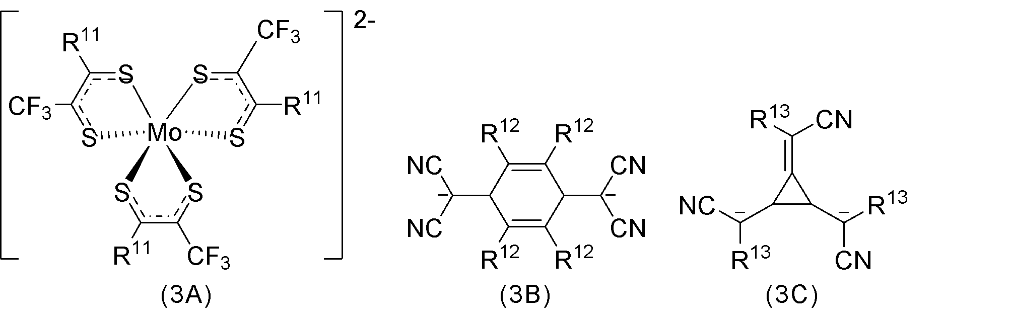
式中、R11は、それぞれ独立して、トリフルオロメチル基(CF3)、メチルオキシカルボニル基(COOMe)、又はトリフルオロメチルオキシカルボニル基(COOCF3)である。
式中、R12は、それぞれ独立して、水素原子、ハロゲン原子、又は置換基を有していてもよいアルキル基であり、好ましくは水素原子又はハロゲン原子であり、より好ましくはハロゲン原子である。
R12で表されるハロゲン原子としては、フッ素原子、塩素原子、臭素原子、及びヨウ素原子等が挙げられ、好ましくはフッ素原子である。
R12で表される置換基を有していてもよいアルキル基は、R1~R3で表される置換基を有していてもよいアルキル基と同義であり、その好ましい態様も同様である。
式中、R13は、それぞれ独立して、シアノ基(CN)又はメチルオキシカルボニル基(COOMe)である。
低分子疎水性閉殻アニオンを生じる第1酸化剤としては、例えば、塩化鉄(III)及び式(4A)~(4C)で表される化合物等が挙げられる。塩化鉄(III)は、FeCl4
-を生じる第1酸化剤であり、式(4A)~(4C)で表される化合物は、それぞれ、式(3A)~(3C)で表される低分子疎水性閉殻カチオンを生じる第1酸化剤である。
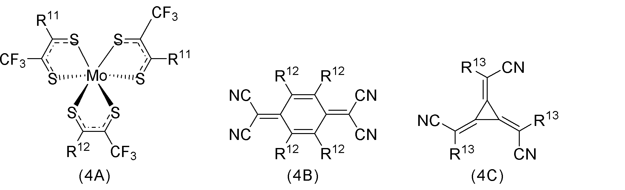
式(4A)中のR11は、式(3A)中のR11と同義であり、その好ましい態様も同様である。
式(4B)中のR12は、式(3B)中のR12と同義であり、その好ましい態様も同様である。
式(4C)中のR13は、式(3C)中のR13と同義であり、その好ましい態様も同様である。
式(4B)中のR12は、式(3B)中のR12と同義であり、その好ましい態様も同様である。
式(4C)中のR13は、式(3C)中のR13と同義であり、その好ましい態様も同様である。
第1酸化剤から生じる低分子疎水性ラジカルアニオンとしては、例えば、式(3D)~(3E)で表されるラジカルアニオンが挙げられる。これらのうち、1酸化剤から生じる低分子疎水性ラジカルアニオンは、式(3D)で表されるラジカルアニオンから選択される1種以上であることが好ましい。
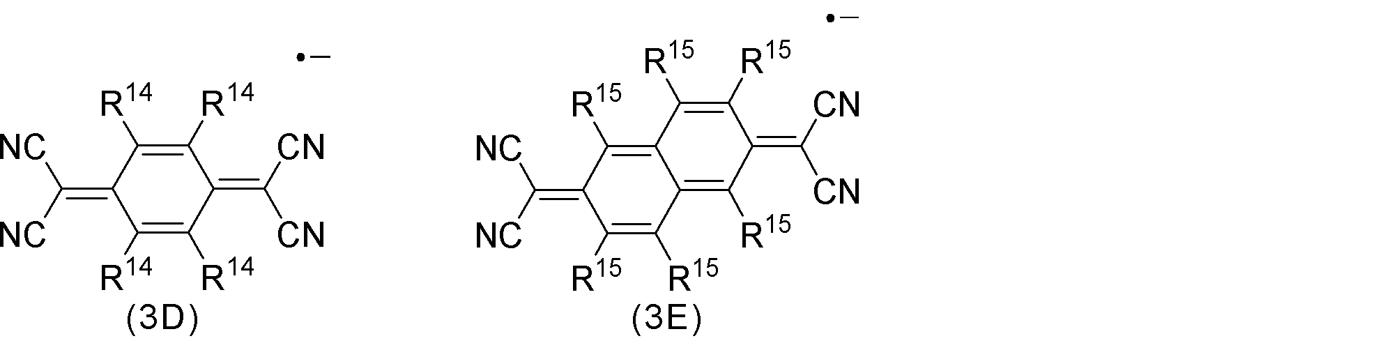
式中、R14及びR15は、それぞれ独立して、水素原子、ハロゲン原子、又は置換基を有していてもよいアルキル基であり、好ましくは水素原子又はハロゲン原子であり、より好ましくはハロゲン原子である。
R14及びR15で表されるハロゲン原子としては、フッ素原子、塩素原子、臭素原子、及びヨウ素原子等が挙げられ、好ましくはフッ素原子である。
R14及びR15で表される置換基を有していてもよいアルキル基は、R1~R3で表される置換基を有していてもよいアルキル基と同義であり、その好ましい態様も同様である。
式(3D)で表される低分子疎水性ラジカルアニオンの具体例としては、下記アニオンが好ましく挙げられる。

式(3E)で表される低分子疎水性ラジカルアニオンの具体例としては、下記アニオンが好ましく挙げられる。

低分子疎水性ラジカルアニオンを生じる第1酸化剤としては、式(4D)~(4E)で表される化合物が挙げられる。式(4D)~(4E)で表される化合物は、それぞれ、式(3D)~(3E)で表される低分子疎水性ラジカルカチオンを生じる第1酸化剤である。したがって、これらのうち、第1酸化剤は、式(4D)で表される化合物から選択される1種以上であることが好ましい。
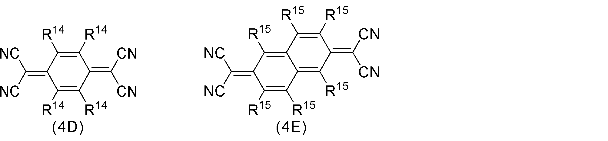
式(4D)中のR14は、式(3D)中のR14と同義であり、その好ましい態様も同様である。
式(4E)中のR15は、式(3E)中のR15と同義であり、その好ましい態様も同様である。
式(4E)中のR15は、式(3E)中のR15と同義であり、その好ましい態様も同様である。
式(4D)で表される化合物の具体例としては、下記化合物が好ましく挙げられる。

式(4E)で表される化合物の具体例としては、下記化合物が好ましく挙げられる。

第1酸化剤は、1種単独で使用してもよく、2種以上を任意の比率及び組み合わせで併用してもよい。したがって、第1電極の表面に付着する低分子疎水性アニオンもまた、1種単独又は2種以上であってよい。
表面修飾液(S2)に含まれる他の低分子疎水性アニオンとしては、第1酸化剤から生じる低分子疎水性アニオンと同義であり、その好ましい態様も同様である。低分子疎水性アニオンは、1種単独で使用してもよく、2種以上を任意の比率及び組み合わせで併用してもよい。ただし、一の表面修飾液(S2)に含まれる他の低分子疎水性アニオンは、第1還元剤由来の低分子疎水性アニオンとは異なるアニオンである。
表面修飾液(S2)に含まれる他の低分子疎水性アニオンの対カチオンとしては、特に限定されないが、例えばプロトン;並びにリチウムイオン、ナトリウムイオン、及びカリウムイオン等の金属イオン;等が挙げられる。これらのうち、対カチオンは、第1電極から有機半導体層へのホール注入を阻害する金属塩の堆積を抑制できる点で、プロトンであることが好ましい。
表面修飾液(S2)中の第1酸化剤の総濃度は、特に限定されず、第1酸化剤の種類、後述する低分子疎水性イオン被覆率、及び仕事関数のシフト幅等に応じて適宜選択すればよい。例えば、第1酸化剤の総濃度は、好ましくは0.01質量%以上3.00質量%以下、より好ましくは0.10質量%以上1.00質量%以下である。
表面修飾液(S2)が他の低分子疎水性アニオンを含む場合、表面修飾液(S2)中の他の低分子疎水性アニオンの総濃度は、特に限定されず、他の低分子疎水性アニオンの種類、後述する低分子疎水性イオン被覆率、仕事関数のシフト幅、及び第1電極を修飾する全低分子疎水性アニオン中の他の低分子疎水性アニオンの割合等に応じて適宜選択すればよい。例えば、低分子疎水性アニオンの総濃度は、好ましくは0.01質量%以上3.00質量%以下、より好ましくは0.10質量%以上1.00質量%以下である。
(表面修飾液(S3))
表面修飾液(S3)に含まれる第2還元剤は、第1電極を還元する化合物であり、低分子疎水性カチオンを生じない化合物である。また、第2還元剤は、第1電極の還元に際し、低分子疎水性カチオン以外のカチオン種をも生じない化合物であることが好ましい。第2還元剤が、カチオン種を生じないことで、表面修飾液(S3)に含まれる低分子疎水性閉殻カチオンを第1電極の表面に選択的に付着させることができるからである。
表面修飾液(S3)に含まれる第2還元剤は、第1電極を還元する化合物であり、低分子疎水性カチオンを生じない化合物である。また、第2還元剤は、第1電極の還元に際し、低分子疎水性カチオン以外のカチオン種をも生じない化合物であることが好ましい。第2還元剤が、カチオン種を生じないことで、表面修飾液(S3)に含まれる低分子疎水性閉殻カチオンを第1電極の表面に選択的に付着させることができるからである。
第2還元剤としては、後述する第3還元剤と同様のものを使用することができ、第3還元剤として好ましい化合物は、第2還元剤としても好ましい。すなわち、第2還元剤としては、第3還元剤として後述するヒドロキノン骨格を有するヒドロキノン化合物;ジヒドロキシフラノン骨格を有するジヒドロキシフラノン化合物;還元性を有する糖類;及び還元型補酵素;等が挙げられ、好ましくはヒドロキノン骨格を有するヒドロキノン化合物及び還元型補酵素からなる群より選択される1種以上であり、より好ましくは還元型補酵素である。
表面修飾液(S3)に含まれる低分子疎水性閉殻カチオンは15℃以上35℃以下の温度条件下(室温条件下)及び大気雰囲気下で水との酸化還元反応及び酸素との酸化還元反応を生じにくいものであることが特に好ましい。
このような低分子疎水性閉殻カチオンとしては、第1還元剤から生じる低分子疎水性閉殻カチオンとして挙げたものの他、式(1D)~(1F)で表される低分子疎水性閉殻カチオンが好ましく挙げられる。

式中、R4~R6は、それぞれ独立して、水素原子、置換基を有していてもよいアルキル基、又は置換基を有していてもよいアリール基である。
R4~R6で表される置換基を有していてもアルキル基及び置換基を有していてもよいアリール基は、それぞれ、R1~R3で表される置換基を有していてもアルキル基及び置換基を有していてもよいアリール基と同義である。
R4~R6で表される置換基を有していてもアルキル基及び置換基を有していてもよいアリール基は、それぞれ、R1~R3で表される置換基を有していてもアルキル基及び置換基を有していてもよいアリール基と同義である。
R4は、好ましくは置換基を有していてもよいアルキル基又は置換基を有していてもよいアリール基であり、より好ましくは置換基を有していてもよいアリール基であり、さらに好ましくは無置換のアリール基である。
R5は、好ましくは置換基を有していてもよいアルキル基又は置換基を有していてもよいアリール基であり、より好ましくは置換基を有していてもよいアリール基であり、さらに好ましくは無置換のアリール基である。
R6は、好ましくは置換基を有していてもよいアルキル基又は置換基を有していてもよいアリール基であり、より好ましくは無置換のアルキル基又は置換基を有していてもよいアリール基である。
R5は、好ましくは置換基を有していてもよいアルキル基又は置換基を有していてもよいアリール基であり、より好ましくは置換基を有していてもよいアリール基であり、さらに好ましくは無置換のアリール基である。
R6は、好ましくは置換基を有していてもよいアルキル基又は置換基を有していてもよいアリール基であり、より好ましくは無置換のアルキル基又は置換基を有していてもよいアリール基である。
式(1D)で表される低分子疎水性閉殻カチオンの具体例としては、下記カチオンが好ましく挙げられる。
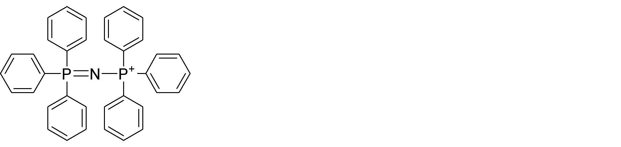
式(1E)で表される低分子疎水性閉殻カチオンの具体例としては、下記カチオンが好ましく挙げられる。

式(1F)で表される低分子疎水性閉殻カチオンの具体例としては、下記カチオンが好ましく挙げられる。

表面修飾液(S3)に含まれる低分子疎水性閉殻カチオンの対アニオンとしては、特に限定されないが、例えば水酸化物イオン;塩化物イオン、臭化物イオン、ヨウ化物イオン等のハロゲン化物イオン;炭酸イオン;硫酸イオン;並びにリン酸イオン;等が挙げられる。これらのうち、対アニオンは、第1電極から有機半導体層への電子注入を阻害するハロゲン化物塩の堆積を抑制できる点で、水酸化物イオンであることが好ましい。
表面修飾液(S3)中の第2還元剤の総濃度は、特に限定されず、第2還元剤の種類及び仕事関数のシフト幅等に応じて適宜選択すればよい。例えば、第2還元剤の総濃度は、好ましくは0.01質量%以上3.00質量%以下、より好ましくは0.10質量%以上1.00質量%以下である。
表面修飾液(S3)中の低分子疎水性閉殻カチオンの総濃度は、特に限定されず、低分子疎水性閉殻カチオンの種類、後述する低分子疎水性イオン被覆率、及び仕事関数のシフト幅等に応じて適宜選択すればよい。例えば、低分子疎水性閉殻カチオンの総濃度は、好ましくは0.01質量%以上3.00質量%以下、より好ましくは0.10質量%以上1.00質量%以下である。
低分子疎水性閉殻カチオンの対アニオンがハロゲン化物イオンである場合、表面修飾液(S3)中のハロゲン化物イオンの総濃度は、好ましくは100質量ppm以下、より好ましくは10質量ppm以下、さらに好ましくは1質量ppm以下である。ハロゲン化物イオンを上記範囲内とすることにより、第1電極の表面上に不要な塩が堆積したり、ハロゲン化物イオンが有機半導体層中に拡散して縦型ダイオードの寿命を短くしたりする不都合を抑制し得る。
表面修飾液として表面修飾液(S3)を使用する場合、本工程では、第1電極に電子が注入されることにより(すなわち、第1電極の表面が還元されることにより)、第1電極の表面が負に帯電する。そして、この負に帯電した第1電極の表面に低分子疎水性閉殻カチオンが静電的に付着し、表面が修飾された第1電極が得られる。このとき、第1電極の表面には、表面修飾液(S1)を使用した場合と同様、低分子疎水性閉殻カチオンが静電的に付着し、厚さが単分子層以下のカチオン層が形成される。カチオン層の厚さは、X線光電子分光法(XPS)分析により求めることができる。
このように、表面修飾液として表面修飾液(S3)を用いる場合も、表面修飾液(S1)した場合と同様に第1電極の表面が修飾される。したがって、表面修飾液として表面修飾液(S3)を用いる場合にも、表面修飾液(S1)した場合と同様にして第1電極の仕事関数を浅く(小さく)することができ、縦型ダイオードの整流特性を向上し得る。また、縦型ダイオードの低電圧における電流密度を高めることも可能となる。
表面修飾液(S3)を用いて第1電極を修飾する場合、有機半導体層として電子輸送性有機半導体の層、すなわち、n型有機半導体の層を用い、第1電極を電子注入電極(カソード(陰極))とすることにより、整流特性に優れた縦型ダイオードを得ることができる。また、低電圧でも高い電流密度を示す縦型ダイオードを得ることができる。このとき、有機半導体層全体がn型有機半導体の層である必要はなく、例えば、有機半導体層が多層構造を有する場合は、第1電極と隣接する層のみがn型有機半導体の層であれば、同様に上記効果が得られる。
第1電極の修飾に表面修飾液(S3)を用いる場合も、表面修飾液(S1)を使用する場合と同様の理由により、第1電極と有機半導体層との間に電子注入を阻害するほどの余剰の層が形成されたり、塩が生じたりする問題が効果的に抑制される。そのため、第1電極から有機半導体層への電子注入性を向上でき、縦型ダイオードの整流特性の向上、長寿命化、及び低電圧における電流密度の向上も実現し得る。
(表面修飾液(S4))
表面修飾液(S4)に含まれる第2酸化剤は、第1電極を酸化する化合物であり、低分子疎水性アニオンを生じない化合物である。また、第2酸化剤は、第1電極の酸化に際し、低分子疎水性アニオン以外のアニオン種をも生じない化合物であることが好ましい。第2酸化剤が、アニオン種を生じないことで、表面修飾液(S4)に含まれる低分子疎水性閉殻アニオンを第1電極の表面に選択的に付着させることができるからである。
表面修飾液(S4)に含まれる第2酸化剤は、第1電極を酸化する化合物であり、低分子疎水性アニオンを生じない化合物である。また、第2酸化剤は、第1電極の酸化に際し、低分子疎水性アニオン以外のアニオン種をも生じない化合物であることが好ましい。第2酸化剤が、アニオン種を生じないことで、表面修飾液(S4)に含まれる低分子疎水性閉殻アニオンを第1電極の表面に選択的に付着させることができるからである。
第2酸化剤としては、後述する第3酸化剤と同様のものを使用することができ、第3酸化剤として好ましい化合物は、第2酸化剤としても好ましい。すなわち、第2酸化剤としては、第3酸化剤として後述するキノン骨格を有するキノン化合物;フラントリオン骨格を有するフラントリオン化合物;及びラジカル化合物;等が挙げられ、好ましくはキノン骨格を有するキノン化合物である。
表面修飾液(S4)に含まれる低分子疎水性閉殻アニオンは、15℃以上35℃以下の温度条件下(室温条件下)及び大気雰囲気下で水との酸化還元反応及び酸素との酸化還元反応を生じにくいものであることが特に好ましい。
このような低分子疎水性閉殻アニオンとしては、第1酸化剤から生じる低分子疎水性閉殻アニオンとして挙げたものの他、式(3F)~(3G)で表される低分子疎水性閉殻アニオンが好ましく挙げられる。

式中、R14は、それぞれ独立して、水素原子、ハロゲン原子、又は置換基を有していてもよいフッ化アルキル基であり、好ましくはハロゲン原子である。
式中、R15は、それぞれ独立して、パーフルオロアルキル基であり、2つのR15は、互いに連結して環を形成していてもよい。
R14で表されるハロゲン原子としては、フッ素原子、塩素原子、臭素原子、及びヨウ素原子等が挙げられ、好ましくは塩素原子又はフッ素原子であり、より好ましくはフッ素原子である。
R14で表されるフッ化アルキル基が有していてもよい置換基としては、R1~R3で表されるアルキル基及びアリール基が有していてもよい置換基と同様のものが挙げられるが、これらに限定されるものではない。なお、フッ化アルキル基において、置換基は、フッ化アルキル基の炭素に結合した水素原子を置換する基である。
R14で表される置換基を有していてもよいフッ化アルキル基の炭素数は、特に限定されないが、好ましくは1以上10以下、より好ましくは1以上6以下、さらに好ましくは2以上4以下である。
R14で表される置換基を有していてもよいフッ化アルキル基の具体例としては、トリフルオロメチル基、ペンタフルオロエチル基、ペンタフルオロ-n-プロピル基、1,1,1,3,3,3-ヘキサフルオロ-2-メトキシ-2-プロピル基等が挙げられ、好ましくはトリフルオロメチル基である。
R15で表されるパーフルオロアルキル基の炭素数は、特に限定されないが、好ましくは1以上20以下、より好ましくは1以上12以下、さらに好ましくは2以上8以下、特に好ましくは2以上6以下である。
R15で表されるパーフルオロアルキル基の具体例としては、パーフルオロメチル基(トリフルオロメチル基)、パーフルオロエチル基、パーフルオロ-n-プロピル基、パーフルオロイソプロピル基、パーフルオロ-n-ブチル基、パーフルオロイソブチル基、パーフルオロ-sec-ブチル基、パーフルオロ-tert-ブチル基、パーフルオロ-n-ペンチル基、パーフルオロネオペンチル基、パーフルオロ-n-ヘキシル基、パーフルオロシクロヘキシル基等が挙げられ、好ましくはパーフルオロメチル基及びパーフルオロ-n-ブチル基である。
式(3F)で表される低分子疎水性閉殻アニオンの具体例としては、テトラフェニルボレートアニオン、テトラキス(p-トリル)ボレートアニオン、テトラキス(p-トリフルオロメチルフェニル)ボレートアニオン、テトラキス(p-フルオロフェニル)ボレートアニオン、テトラキス(パーフルオロフェニル)ボレートアニオン、及びテトラキス[3,5-ビス(トリフルオロメチル)フェニル]ボレートアニオン等が挙げられ、好ましくはテトラキス[3,5-ビス(トリフルオロメチル)フェニル]ボレートアニオンである。
式(3G)で表される低分子疎水性閉殻アニオンの具体例としては、ビス(トリフルオロメタンスルホニル)イミドアニオン、ビス(パーフルオロエタンスルホニル)イミドアニオン、ビス(パーフルオロプロパンスルホニル)イミドアニオン、ビス(パーフルオロブタンスルホニル)イミドアニオン、及びシクロヘキサフルオロプロパン-1,3-ビス(スルホニル)イミドアニオン等が挙げられ、好ましくはビス(トリフルオロメタンスルホニル)イミドアニオンである。
表面修飾液(S4)に含まれる低分子疎水性閉殻アニオンの対カチオンとしては、特に限定されないが、例えばプロトン;並びにリチウムイオン、ナトリウムイオン、及びカリウムイオン等の金属イオン;等が挙げられる。これらのうち、対カチオンは、第1電極から有機半導体層へのホール注入を阻害する金属塩の堆積を抑制できる点で、プロトンであることが好ましい。
低分子疎水性閉殻アニオンの対カチオンが金属イオンである場合、表面修飾液(S3)中の当該金属イオンの総濃度は、好ましくは10,000質量ppm以下、より好ましくは1,000質量ppm以下、さらに好ましくは100質量ppm以下である。金属イオンを上記範囲内とすることにより、第1電極の表面上に不要な塩が堆積したり、金属イオンが有機半導体層中に拡散して縦型ダイオードの寿命を短くしたりする不都合を抑制し得る。
表面修飾液(S4)中の第2酸化剤の総濃度は、特に限定されず、第2酸化剤の種類及び仕事関数のシフト幅等に応じて適宜選択すればよい。例えば、第2酸化剤の総濃度は、好ましくは0.01質量%以上3.00質量%以下、より好ましくは0.10質量%以上1.00質量%以下である。
表面修飾液(S4)中の低分子疎水性閉殻アニオンの総濃度は、特に限定されず、低分子疎水性閉殻アニオンの種類、後述する低分子疎水性イオン被覆率、及び仕事関数のシフト幅等に応じて適宜選択すればよい。例えば、低分子疎水性閉殻アニオンの総濃度は、好ましくは0.01質量%以上3.00質量%以下、より好ましくは0.10質量%以上1.00質量%以下である。
表面修飾液として表面修飾液(S4)を用いる場合、本工程では、第1電極にホールが注入されることにより(すなわち、第1電極の表面が酸化されることにより)、第1電極の表面が正に帯電する。そして、この正に帯電した第1電極の表面に、低分子疎水性閉殻アニオンが静電的に付着し、表面が修飾された第1電極が得られる。このとき、第1電極の表面には、表面修飾液(S2)を使用した場合と同様、低分子疎水性閉殻アニオンが静電的に付着し、厚さが単分子層以下のアニオン層が形成される。アニオン層の厚さは、X線光電子分光法(XPS)分析により求めることができる。
このように、表面修飾液として表面修飾液(S4)を用いる場合も、表面修飾液(S2)した場合と同様に第1電極の表面が修飾される。したがって、表面修飾液として表面修飾液(S4)を用いる場合にも、表面修飾液(S2)した場合と同様にして第1電極の仕事関数を深く(大きく)することができ、縦型ダイオードの整流特性を向上し得る。また、縦型ダイオードの低電圧における電流密度を高めることも可能となる。
表面修飾液(S4)を用いて第1電極を修飾する場合、有機半導体層としてホール輸送性有機半導体の層、すなわち、p型有機半導体の層を用い、第1電極をホール注入電極(アノード(陽極))とすることにより、整流特性に優れた縦型ダイオードを得ることができる。このとき、有機半導体層全体がp型有機半導体の層である必要はなく、例えば、有機半導体層が多層構造を有する場合は、第1電極と隣接する層のみがp型有機半導体の層であれば、同様に上記効果が得られる。
第1電極の修飾に表面修飾液(S4)を使用する場合も、表面修飾液(S2)を使用する場合と同様の理由により、第1電極と有機半導体層との間にホール注入を阻害するほどの余剰の層が形成されたり、塩が生じたりする問題が効果的に抑制される。そのため、第1電極から有機半導体層へのホール注入性を向上でき、縦型ダイオードの整流特性の向上、長寿命化、及び低電圧における電流密度の向上も実現し得る。
(溶媒)
表面修飾液(S1)~(S4)の溶媒は、有機溶媒であってもよく、水であってもよく、有機溶媒と水との混合溶媒であってもよいが、製造コスト抑制、作業性向上、及び環境負荷低減の観点から、好ましくは水である。
表面修飾液(S1)~(S4)の溶媒は、有機溶媒であってもよく、水であってもよく、有機溶媒と水との混合溶媒であってもよいが、製造コスト抑制、作業性向上、及び環境負荷低減の観点から、好ましくは水である。
水としては、特に限定されず、水道水;蒸留水、RO水、及び脱イオン水等の純水;並びに比抵抗18MΩ以上の超純水;等を使用し得るが、好ましくは純水、より好ましくは脱イオン水である。なお、本開示において、RO水とは、逆浸透膜でろ過した水を意味する。
有機溶媒としては、低分子還元剤又は低分子酸化剤を溶解又は分散し得る限り特に限定されず、例えば、メタノール、エタノール、及びn-プロパノール等のアルコール;ヘキサン、ベンゼン、トルエン、及びキシレン等の炭化水素類;ジエチルエーテル、1,4-ジオキサン、ジグリム、及びテトラヒドロフラン(THF)等のエーテル類;酢酸エチル及び酢酸ブチル等のエステル類;アセトン、メチルエチルケトン、及びメチルイソブチルケトン等のケトン類;1,2-ジクロロエタン及びクロロホルム等のハロゲン化炭化水素溶媒類;アセトニトリル及びベンゾニトリル等のニトリル溶媒類;N,N-ジメチルホルムアミド(DMF)、N,N-ジメチルアセトアミド(DMA)、及びN-メチル-2-ピロリドン(NMP)等のアミド類;並びにジメチルスルホキシド(DMSO)等のスルホキシド類;等が挙げられる。
混合溶媒に含まれる有機溶媒としては、上述の有機溶媒のうち水と混和するものを使用できる。混合溶媒中の水の含有量は、両者が均一に混合し得る限り特に限定されず、例えば5質量%以上100質量%未満、40質量%以上95質量%以下、60質量%以上90質量%以下、及び80質量%以上90質量%以下の範囲が挙げられる。
(他の成分)
表面修飾液(S1)~(S4)は、本開示の効果を阻害しない範囲において、上述した成分以外の他の成分を1種以上含んでいてもよい。
表面修飾液(S1)~(S4)は、本開示の効果を阻害しない範囲において、上述した成分以外の他の成分を1種以上含んでいてもよい。
(表面修飾液の調整)
表面修飾液(S1)及び(S2)は、それぞれ、第1還元剤及び第2酸化剤を溶媒に溶解することにより調製される。
表面修飾液(S1)及び(S2)は、それぞれ、第1還元剤及び第2酸化剤を溶媒に溶解することにより調製される。
表面修飾液(S3)は、第2還元剤及び低分子疎水性カチオンをカチオン成分として含む化合物とを溶媒に溶解することにより調製される。当該化合物は、低分子疎水性カチオンと、水酸化物イオン;塩化物イオン、臭化物イオン、ヨウ化物イオン等のハロゲン化物イオン;炭酸イオン;硫酸イオン;並びにリン酸イオン等のアニオン成分とから形成される塩であることが好ましく、入手容易性及びコストの観点から、低分子疎水性カチオンとハロゲン化物イオンとから形成されるハロゲン化物塩であることがより好ましい。
表面修飾液(S3)の調製にハロゲン化物塩を用いた場合、得られる表面修飾液(S3)には、低分子疎水性カチオンの対アニオンとしてハロゲン化物イオンが含まれる。そのため、表面修飾液(S3)の調製にハロゲン化物塩を用いる場合には、ハロゲン化物塩を溶媒に溶解して得られた溶液とアニオン交換樹脂とを接触させ、溶液中のハロゲン化物イオンを水酸化物イオンに交換することで、ハロゲン化物イオンの総濃度を上述した好ましい範囲まで低減することが好ましい。アニオン交換樹脂としては、公知のアニオン交換樹脂等の任意のものを使用することができる。
表面修飾液(S4)は、第2酸化剤及び低分子疎水性アニオンをアニオン成分として含む化合物とを溶媒に溶解することにより調製される。当該化合物は、入手容易性及びコストの観点から、低分子疎水性アニオンとリチウムイオン、ナトリウムイオン、及びカリウムイオン等の金属イオンとから形成される金属塩であることが好ましい。
表面修飾液(S4)の調製に金属塩を用いた場合、得られる表面修飾液(S4)には、低分子疎水性アニオンの対カチオンとして金属イオンが含まれる。そのため、表面修飾液(S4)の調製に金属塩を用いる場合には、金属塩を溶媒に溶解して得られた溶液とカチオン交換樹脂とを接触させ、溶液中の金属イオンをプロトンに交換することで、金属イオンの総濃度を上述した好ましい範囲まで低減することが好ましい。カチオン交換樹脂としては、公知のカチオン交換樹脂等の任意のものを使用することができる。
〔1-1-2.第1電極〕
縦型ダイオードにおいて良好な整流特性を得るためには、一般的に、カソードは、有機半導体層を構成する有機半導体のLUMOよりも小さい仕事関数を有し、かつ、アノードより小さい仕事関数を有することが望ましい。また、アノードは、有機半導体層を構成する有機半導体のLUMOより大きい仕事関数を有することも望ましい。
縦型ダイオードにおいて良好な整流特性を得るためには、一般的に、カソードは、有機半導体層を構成する有機半導体のLUMOよりも小さい仕事関数を有し、かつ、アノードより小さい仕事関数を有することが望ましい。また、アノードは、有機半導体層を構成する有機半導体のLUMOより大きい仕事関数を有することも望ましい。
したがって、第1電極がカソード(陰極;電子注入電極)である場合、第1電極は、電極修飾工程後に、有機半導体層を構成する有機半導体(有機半導体層が多層構造を有する場合は、第1電極に隣接する層を構成する有機半導体)のLUMOより小さい仕事関数を有し、かつ、第2電極より小さい仕事関数を有することが望ましい。また、第1電極がアノード(陽極;ホール注入電極)である場合、第1電極は、第2電極及び有機半導体層を構成する有機半導体(有機半導体層が多層構造を有する場合は、第2電極に隣接する層を構成する有機半導体)よりも大きい仕事関数を示すことが望ましい。
このように、第1電極を構成する材料は、有機半導体及び第2電極に応じて適宜選択されるものであるが、本工程により第1電極の仕事関数を大幅にシフトさせ、所望の仕事関数に容易に調整することが可能であるため、導電性を有する材料である限り特に限定されない。具体的な電極材料としては、例えば、白金、金、銀、アルミニウム、クロム、ニッケル、銅、チタン、マグネシウム、モリブデン、及びタングステン等の金属;これらの金属のうち2種以上を含む合金;並びに酸化インジウム、酸化スズ、酸化亜鉛、インジウムスズ酸化物(ITO)、及びインジウム亜鉛酸化物(IZO)等の金属酸化物;等が挙げられる。
例えば、後述する実施例に示されるように、低分子還元剤を含む表面修飾液との接触により、金電極の仕事関数を約5.0eVから約3.7eVにシフトさせることができるため、表面が修飾された金電極、LUMOが約4.0の有機半導体の層、及び未修飾の金電極を、それぞれ、第1電極、有機半導体層、及び第2電極として用いることで、整流特性に優れた縦型ダイオード、好ましく整流特性に優れ、低電圧における電流密度の高い縦型ダイオードが得られる。また、表面が修飾された金電極を、表面が修飾された銅電極や表面が修飾されたITO電極に代えても、同様の原理により、整流特性に優れた縦型ダイオードが得られる。
従来、縦型ダイオードの電極としては、金及び銀等の貴金属で構成された電極を使用することが通常であり、銅及びITO等は、電極材料として利用できないとされてきた。これに対し、本実施形態によれば、銅及びITOのようなより安価な材料で構成された電極であっても、電極に上述の表面修飾を施すことにより、縦型ダイオードに好適に利用することができようになる。したがって、本実施形態によって、整流特性が良好な縦型ダイオードであって、第1電極及び第2電極のいずれか又は両方が銅電極又はITO電極である縦型ダイオード、好ましくは第1電極が銅電極又はITO電極である縦型ダイオードを提供することができる。
第1電極の厚さは、特に限定されず、縦型ダイオードの用途及び素子寿命等を勘案して適宜調整すればよい。第2電極の具体的な厚さとしては、例えば、10nm以上200nm以下が挙げられ、好ましくは20nm以上50nm以下である。
第2電極は、公知の方法及びこれに準じた方法等の任意の方法により作製することができる。第2電極を作製するための公知の方法としては、例えば、真空蒸着法、スパッタリング、化学蒸着法、及びメッキ法等が挙げられる。
〔1-1-3.操作手順及び条件〕
第1電極の表面と表面修飾液とを接触させる方法は、特に限定されず、公知の溶液プロセス及びこれに準じたプロセス等の任意のプロセスから適宜選択することができる。公知の溶液プロセスとしては、例えば、第1の電極を表面修飾液に浸漬する方法;並びにスピンコート法、スプレーコート法、及びロールコート法等の任意の塗布法により表面修飾液を第1電極に塗布する方法;等が挙げられる。
第1電極の表面と表面修飾液とを接触させる方法は、特に限定されず、公知の溶液プロセス及びこれに準じたプロセス等の任意のプロセスから適宜選択することができる。公知の溶液プロセスとしては、例えば、第1の電極を表面修飾液に浸漬する方法;並びにスピンコート法、スプレーコート法、及びロールコート法等の任意の塗布法により表面修飾液を第1電極に塗布する方法;等が挙げられる。
電極修飾工程は、アルゴン及び窒素等の不活性雰囲気下の他、大気雰囲気下で行うこともできる。上述したように、本工程により得られる表面修飾電極は、水及び大気に対する安定性が高いため、大気雰囲気下、水溶液を用いた溶液プロセスにより電極修飾工程を行ったとしても、表面修飾の効果を十分に得ることができる。したがって、作業性が良好であり、かつ、工業化に有利な点で、電極修飾工程は、大気雰囲気下で行うことが好ましい。
第1電極の表面と表面修飾液とを接触させる際の温度は、特に限定されないが、好ましくは5℃以上50℃以下、より好ましくは15℃以上35℃以下である。
また、第1電極の表面と表面修飾液とを接触させる時間は、特に限定されないが、好ましくは1秒以上10時間以下である。
また、第1電極の表面と表面修飾液とを接触させる時間は、特に限定されないが、好ましくは1秒以上10時間以下である。
第1電極の表面と表面修飾液との接触条件は、第1電極の表面であって縦型ダイオードを作製した際に有機半導体層と隣接する面に占める低分子疎水性イオンの割合、すなわち、当該面の低分子疎水性イオンの層による被覆率(以下、「低分子疎水性イオン被覆率」と称することがある。)が、後述する範囲内となるよう調整されることが好ましい。低分子疎水性イオン被覆率を所定の範囲内とすることで、第1電極の仕事関数を大きく変化させることが可能となるからである。
低分子疎水性イオン被覆率の調整は、低分子疎水性イオンの濃度;酸化剤又は還元剤の濃度;及び溶媒に水を含む場合には溶媒のpH調整;等により行うことができる。電極表面を酸化する場合にはpHが低いほどに被覆率が高まる傾向にあり、還元する場合にはpHが高いほどに被覆率が高まる傾向にある。
〔1-2.ドーピング工程〕
本実施形態では、製造する縦型ダイオードの有機半導体層は、ドープ層とアンドープ層とを有することが好ましい。したがって、本実施形態に係る製造方法は、第3酸化剤及び第3還元剤からなる群より選択される1種以上並びにドーパントイオンの塩を含む水溶液(以下、「ドープ溶液」と称することがある。)と、有機半導体層前駆体の表面とを接触させることで、前記ドープ層を形成するドーピング工程を含むことが好ましい。ドーピング工程においてドープ溶液と接触させる有機半導体層の表面は、縦型ダイオードを作製した際に第2電極と隣接する面である。
本実施形態では、製造する縦型ダイオードの有機半導体層は、ドープ層とアンドープ層とを有することが好ましい。したがって、本実施形態に係る製造方法は、第3酸化剤及び第3還元剤からなる群より選択される1種以上並びにドーパントイオンの塩を含む水溶液(以下、「ドープ溶液」と称することがある。)と、有機半導体層前駆体の表面とを接触させることで、前記ドープ層を形成するドーピング工程を含むことが好ましい。ドーピング工程においてドープ溶液と接触させる有機半導体層の表面は、縦型ダイオードを作製した際に第2電極と隣接する面である。
ドーピング工程では、ドープ溶液と有機半導体層前駆体の表面とを接触させることにより、有機半導体の酸化反応又は還元反応が進行し(すなわち、有機半導体層前駆体にキャリアが注入され)、これに伴い、有機半導体層前駆体にドーパントイオンが導入されることで、ドープ層が形成される。本工程は、大気雰囲気下で行ったとしても、効率のよいドーピングを実現できる。
従来、酸化剤及び還元剤から選択される1種以上を用いた有機半導体の化学ドーピングは、アルゴン及び窒素等の不活性雰囲気下、有機溶媒系で行われてきた。国際公開第2020/085342号に記載のドーピング方法は、イオン交換を用いた化学ドーピングによって、優れたドーピング効率を達成し、優れた特性を有する導電性ポリマーが得られるものの、ドーピングは有機溶媒系及び窒素雰囲気下で行う必要があった。これは、一般的に有機半導体の化学ドーピングに使用される酸化剤及び還元剤が、大気及び水に対して不安定であり、大気雰囲気下での化学ドーピングに適さないからである。一方で、大気及び水の存在下でも使用できる酸化剤及び還元剤は、一般的な有機半導体にキャリアを注入するのに十分な酸化力及び還元力を有しないと認識されていた。
これに対し、本実施形態におけるドーピング工程は、pH調整された水溶液中において電子移動若しくはプロトン共役電子移動により有機半導体を酸化する第3酸化剤、又は電子移動若しくはプロトン共役電子移動により有機半導体を還元する第3還元剤と、ドーピングイオンの塩とを共存させることにより、これらの相乗効果が発揮され、酸素及び水の存在下での有機半導体の化学ドーピングを可能ならしめたものである。
〔1-2-1.ドープ溶液〕
ドーピング工程で用いられるドープ溶液は、第3酸化剤及び第3還元剤から選択される1種以上とドーパントイオンの塩とを含む水溶液である。
ドーピング工程で用いられるドープ溶液は、第3酸化剤及び第3還元剤から選択される1種以上とドーパントイオンの塩とを含む水溶液である。
(第3酸化剤及び第3還元剤)
第3酸化剤は、有機半導体層前駆体にホールを注入し、有機半導体を酸化する化合物である。第3還元剤は、有機半導体層前駆体に電子を注入し、有機半導体層を構成する有機半導体を還元する化合物である。
第3酸化剤は、有機半導体層前駆体にホールを注入し、有機半導体を酸化する化合物である。第3還元剤は、有機半導体層前駆体に電子を注入し、有機半導体層を構成する有機半導体を還元する化合物である。
これらの化合物が有機半導体を酸化又は還元する際、k個のプロトン及びk個の電子が協奏的に移動する。kは、1以上の整数であり、好ましくは1以上4以下、より好ましくは1以上2以下である。例えば、後述するように、第3酸化剤であるベンゾキノンは、2個のプロトン及び2個の電子が協奏的に移動し、有機半導体を酸化する。第3酸化剤は、kの異なる2種以上の第3酸化剤を併用することが好ましい。また、第3還元剤は、kの異なる2種以上の第3還元剤を併用することが好ましい。これにより、ドープ溶液のpH等の外部条件がドーピングに与える影響を低減することが可能となる。
ドーピング工程において、p型有機半導体層にドープ層を形成する場合、第3酸化剤により有機半導体層前駆体にホールを注入し、有機半導体層前駆体を酸化する。一方、ドーピング工程において、n型の有機半導体層にドープ層を形成する場合、第3還元剤により有機半導体層前駆体に電子を注入し、有機半導体層前駆体を還元する。
第3酸化剤及び第3還元剤としては、電子移動又はプロトン共役電子移動により酸化反応又は還元反応を起こす化合物である限り特に限定されず、任意の化合物を使用することができる。好適な第3酸化剤としては、プロトンが関与する酸化反応又は還元反応を起こす化合物(すなわち、ネルンストの式で記述される酸化還元電位がpHに比例する化合物)であって、酸化還元電位が有機半導体のHOMO準位にマッチングする化学種(すなわち、酸化剤として働く化学種)が挙げられる。好適な第3還元剤としては、プロトンが関与する還元反応を起こす化合物(すなわち、ネルンストの式で記述される酸化還元電位がpHに比例する化合物)であって、酸化還元電位が有機半導体のLUMO準位にマッチングする化学種(すなわち、還元剤として働く化学種)が挙げられる。
第3酸化剤としては、例えば、キノン骨格を有するキノン化合物(k=2);フラントリオン骨格を有するフラントリオン化合物(k=2);及びラジカル化合物;等が挙げられ、好ましくはキノン骨格を有するキノン化合物である。
キノン化合物としては、例えば、式(Q1)~(Q4)で表される化合物が挙げられる。
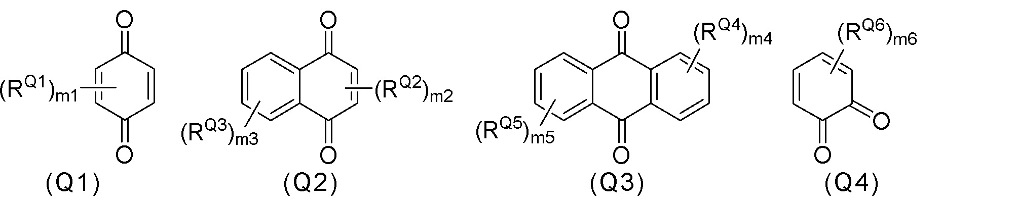
式中、RQ1~RQ6は、それぞれ独立して、1価の官能基であり;m1は、0~4の整数であり;m2は、0~2の整数であり;m3は、0~4の整数であり;m4は、0~4の整数であり;m5は、0~4の整数であり;m6は、0~4の整数である。
式中、RQ1~RQ6は、それぞれ独立して、1価の官能基である。隣接するRQ1~RQ6は、互い結合して環を形成してもよい。形成される環は、5員環~7員環が好ましい。
RQ1~RQ6で表される1価の官能基としては、特に限定されないが、アルキル基(炭素数1~12が好ましく、1~6がより好ましい)、アルケニル基(炭素数2~12が好ましく、2~6がより好ましい)、アリール基(炭素数6~22が好ましく、6~14がより好ましい)、アラルキル基(炭素数6~22が好ましく、6~14がより好ましい)、アルコキシ基(炭素数1~12が好ましく、1~6がより好ましい)、ヒドロキシ基、カルボキシ基、メルカプト基、アミノ基、ハロゲン原子(塩素原子、臭素原子等)、アルキルエーテル基、カルボン酸エステル基、スルホン酸基、ホルミル基、ニトロ基、シアノ基、及びシリル基等が挙げられる。また、1価の官能基は、上記官能基が-O-、-NR-、-S-、-CO-、-COO-、及び-CONH-等の2価の連結基を介して結合された基であってもよい。なお、アルキル基及びアルケニル基は、直鎖状、分岐状、及び環状のいずれであってもよい。
RQ1~RQ6のうち1以上は、アルキル基、アルコキシ基、アルキルエーテル基、カルボン酸エステル基、ハロゲン原子、ヒドロキシ基、アミノ基、カルボキシ基、スルホン酸基、アルデヒド基、ニトロ基、シアノ基、チオール基、及びシリル基から選択される1種以上であることが好ましい。
RQ1~RQ6のうち、1以上をアルコキシ基、ヒドロキシ基、カルボキシ基、スルホン酸基、及びアミノ基等の親水基とすることにより、化合物の親水性を調整でき好ましい。
RQ1~RQ6のうち、1以上を電子求引基又は電子供与基とすることにより、化合物の酸化還元電位を調整でき好ましい。電子求引基は、化合物の酸化力を高め、還元力を弱める。逆に、電子供与基は、化合物の酸化力を弱め、還元力を高める。
すなわち、使用する有機半導体のHOMO準位又はLUMO準位にマッチングするようにRQ1~RQ6を選択し、酸化還元作用を調整することができる。
すなわち、使用する有機半導体のHOMO準位又はLUMO準位にマッチングするようにRQ1~RQ6を選択し、酸化還元作用を調整することができる。
m1は、0~4の整数であり、好ましくは0~2の整数、より好ましくは0~1の整数である。
m2は、0~2の整数であり、好ましくは0~1の整数である。
m3は、0~4の整数であり、好ましくは0~2の整数、より好ましくは0~1の整数である。
m4は、0~4の整数であり、好ましくは0~2の整数、より好ましくは0~1の整数である。
m5は、0~4の整数であり、好ましくは1~2の整数である。
m6は、0~4の整数であり、好ましくは0~2の整数、より好ましくは0~1の整数である。
m2は、0~2の整数であり、好ましくは0~1の整数である。
m3は、0~4の整数であり、好ましくは0~2の整数、より好ましくは0~1の整数である。
m4は、0~4の整数であり、好ましくは0~2の整数、より好ましくは0~1の整数である。
m5は、0~4の整数であり、好ましくは1~2の整数である。
m6は、0~4の整数であり、好ましくは0~2の整数、より好ましくは0~1の整数である。
キノン化合物の具体例としては、p-ベンゾキノン、2,5-ジヒドロキシ-p-ベンゾキノン、2-ヒドロキシ-p-ベンゾキノン、テトラヒドロキシ-p-ベンゾキノン、1,4-ナフトキノン、2-ヒドロキシ-1,4-ナフトキノン、2-メチル-p-ベンゾキノン、2-メチル-1,4-ナフトキノン、2,5-ジメトキシ-1,4-ベンゾキノン、2,5-ジ-tert-ブチル-1,4-ナフトキノン、及びアントラキノン等が挙げられる。また、特表第2018-520455号公報に記載のキノン化合物も、本実施形態における第3酸化剤として利用できる。
フラントリオン化合物としては、式(Q5)で表される化合物が挙げられる。

式中、RQ7及びRQ8は、それぞれ、水素原子又は1価の官能基である。RQ7及びRQ8で表される1価の官能基は、RQ1~RQ6で表される1価の官能基と同義であり、その好ましい態様も同様である。
式(Q5)で表される化合物の具体例としては、例えば、デヒドロアスコルビン酸等が挙げられる。
ラジカル化合物としては、例えば、2,2-ジフェニル-1-ピクリルヒドラジル(DPPH)、4-ヒドロキシ-2,2,6,6-テトラメチル-ピペリジン1-オキシル(TEMPOL)、2,2,6,6テトラメチル-ピペリジニルオキシル(TEMPO)、2,6-ジ-tert-ブチル-α-(3,5-ジ-tert-ブチル-4-オキソ-2,5-シクロヘキサジエン-1-イリデン)-p-トリルオキシ,フリーラジカル(ガルビノキシル,フリーラジカル)、及びトリフェニルメチルラジカル等が挙げられる。
ラジカル化合物は、水溶液中でより効率的に反応が進行しやすい点で、酸素原子上にラジカルを含む化合物であることが好ましく、式(F1)で表される化合物及び式(F2)で表される化合物(k=1)から選択される1種以上であることがより好ましい。
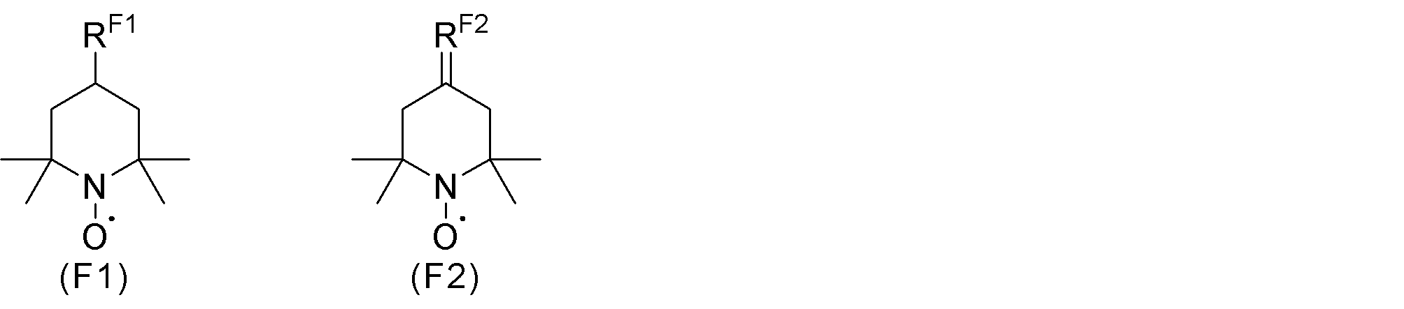
式中、RF1は、1価の官能基であり;RF2は、O又はSであり、好ましくはOである。
RF1で表される1価の官能基としては、特に限定されないが、水素原子、ヒドロキシ基、カルボキシ基、アミノ基、(メタ)アクリロイル基、(メタ)アクリルアミド基、ヘテロ原子を有していてもよい炭素数1~20の炭化水素基、及び炭素数1~20のアルコキシ基等が好ましく挙げられる。
RF1は、式(F1)で表される化合物の水溶性が向上する点で、親水基であることが好ましい。親水基としては、例えば、ヒドロキシ基、カルボキシ基、(メタ)アクリロイル基、(メタ)アクリルアミド基、及びアルコキシ基(メトキシ基、エトキシ基)等が好ましく挙げられる。
式(F1)で表される化合物及び式(F2)で表される化合物としては、合成品を使用してもよく、2,2,6,6-テトラメチルピペリジン1-オキシル(TEMPO)、4-メタクリロイルオキシ-2,2,6,6-テトラメチルピペリジン-1-オキシル(メタクリル酸TEMPO)、4-アセトアミド-TEMPO、4-ヒドロキシ-TEMPO(TEMPOL)、4-オキソ-TEMPO、4-ヒドロキシ-TEMPOベンゾアート、4-(2-ヨードアセトアミド)-TEMPO、4-アミノ-TEMPO、及び4-カルボキシ-TEMPO等の市販品を使用してもよい。
第3酸化剤は、1種単独で使用してもよく、2種以上を任意の比率及び組み合わせで併用してもよい。
第3酸化剤は、キノン化合物及びフラントリオン化合物から選択される1種以上であることが好ましく、式(Q1)~(Q5)で表される化合物から選択される1種以上であることが好ましく、式(Q1)で表される化合物から選択される1種以上であることが好ましい。
また、式(Q1)~(Q5)で表される化合物は、その還元体とともにドープ溶液に含まれることが好ましい。これにより、式(Q1)~(Q5)で表される化合物のレドックスポテンシャルをより精密に制御でき、結果として、ドープ層に含まれる有機半導体のフェルミ準位をより精密に制御することができる。
第3還元剤としては、例えば、ヒドロキノン骨格を有するヒドロキノン化合物(k=2);ジヒドロキシフラノン骨格を有するジヒドロキシフラノン化合物(k=2);還元性を有する糖類;及び還元型補酵素;等が挙げられ、好ましくはヒドロキノン骨格を有するヒドロキノン化合物及び還元型補酵素からなる群より選択される1種以上であり、より好ましくは還元型補酵素である。
ヒドロキノン化合物としては、例えば、式(Q1’)~(Q4’)で表される化合物が挙げられる。式(Q1’)~(Q4’)で表される化合物は、それぞれ、式(Q1)~(Q4)で表される化合物の還元体である。

式中、RQ1~RQ6は、それぞれ、式(Q1)~(Q4)中のRQ1~RQ6と同義であり、その好ましい態様も同様である。
ヒドロキノン化合物の具体例としては、p-ヒドロキノン、1,2,4,5-ベンゼンテトラオール、1,2,4-ベンゼントリオール、ベンゼンヘキサオール、1,4-ナフタレンジオール、1,2,5-ナフタレントリオール、2-メチル-1,4-ベンゼンジオール、2-メチル-1,4-ナフタレンジオール、2,5-ジメトキシ-1,4-ベンゼンジオール、2,5-ジ-tert-ブチル-1,4-ナフタレンジオール、及び9,10-アントラセンジオール等が挙げられる。また、特表第2018-520455号公報に記載のキノン化合物の還元体も、本実施形態における第3還元剤として利用できる。
ジヒドロキシフラノン化合物としては、式(Q5’)で表される化合物が挙げられる。式(Q5’)で表される化合物は、式(Q5)で表される化合物の還元体である。
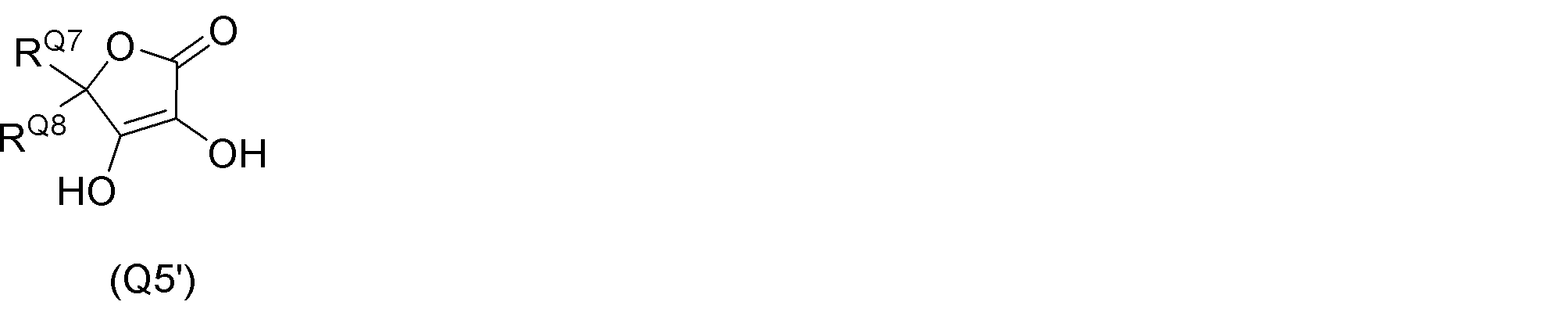
式中、RQ7及びR8は、それぞれ、式(Q5)中のRQ7及びR8と同義であり、その好ましい態様も同様である。
式(Q5’)で表される化合物の具体例としては、アスコルビン酸等が挙げられる。
還元性を有する糖類としては、例えば、フルクトース、グルコース、ガラクトース、マルトース、ラクトース、及びセロビオース等が挙げられ、好ましくはフルクトースである。
還元型補酵素としては、例えば、還元型フラビンモノヌクレオチド(FMNH2)、還元型フラビンアデニンジヌクレオチド(FADH2)、還元型ニコチンアミドアデニンジヌクレオチド、及び還元型ニコチンアミドアデニンジヌクレオチドリン酸(NADPH)等が挙げられ、好ましくは還元型フラビンモノヌクレオチド(FMNH2)である。還元型補酵素は、還元性を有する糖類等を用いるなどして酸化型補酵素を還元することにより発生させることができる。例えば、フルクトースと酸化型フラビンモノヌクレオチド(FMN)とを水に溶解すると、酸化型フラビンモノヌクレオチドがフルクトースから電子を受け取ることにより、系内で還元型フラビンモノヌクレオチドが生じ、この還元型フラビンモノヌクレオチドが有機半導体層前駆体に電子を注入する。
第3還元剤は、1種単独で使用してもよく、2種以上を任意の比率及び組み合わせで併用してもよい。
第3還元剤は、ヒドロキノン化合物及びジヒドロキシフラノン化合物から選択される1種以上であることが好ましく、式(Q1’)~(Q5’)で表される化合物から選択される1種以上であることが好ましく、式(Q1’)で表される化合物から選択される1種以上であることが好ましい。
また、式(Q1’)~(Q5’)で表される化合物は、その酸化体とともにドープ溶液に含まれることが好ましい。これにより、式(Q1’)~(Q5’)で表される化合物のレドックスポテンシャルをより精密に制御でき、結果として、ドープ層に含まれる有機半導体のフェルミ準位をより精密に制御することができる。
ドープ溶液は、ドーパントイオンの塩とともに、第3酸化剤及び第3還元剤の一方を含んでいればよいが、第3酸化剤及び第3還元剤の両方を含むことも好ましい。ドープ溶液が第3酸化剤及び第3還元剤の両方を含むことにより、ドープ溶液の酸化還元電位及び有機半導体のフェルミ準位をより安定的に制御し得るからである。ドープ溶液が第3酸化剤及び第3還元剤の両方を含む場合は、有機半導体層前駆体に注入すべきキャリア及びドーパントイオンに応じて、第3酸化剤と第3還元剤との比率を調整すればよい。
ドープ溶液中の第3酸化剤及び第3還元剤の総含有量は、特に限定されないが、ドーピング効率向上の観点から、0.01~1,000mMが好ましい。なお、ドープ溶液に含まれる第3酸化剤及び第3還元剤は、溶媒である水に完全に溶解していることが好ましいが、その一部が固体の状態でドープ溶液中に含まれていてもよい。
(ドーパントイオンの塩)
ドーパントイオン塩は、最終的に有機半導体層に導入されるドーパントイオンと、その対イオンであるスペクテータイオンとの共存塩である。ドーパントイオンは、閉殻イオンであることが好ましく、疎水性閉殻イオンであることがより好ましい。スペクテータイオンは、有機半導体に導入されないイオンである。
ドーパントイオン塩は、最終的に有機半導体層に導入されるドーパントイオンと、その対イオンであるスペクテータイオンとの共存塩である。ドーパントイオンは、閉殻イオンであることが好ましく、疎水性閉殻イオンであることがより好ましい。スペクテータイオンは、有機半導体に導入されないイオンである。
有機半導体層がp型有機半導体の層である場合、ドーパントイオンは、スペクテータイオンと塩を形成し得る閉殻アニオンであることが好ましく、スペクテータイオンと塩を形成し得る疎水性閉殻アニオンであることがより好ましい。
このようなドーパントイオンとしては、例えば、ビス(トリフルオロメタンスルホニル)イミドイオン(TFSIイオン)、テトラフルオロホウ酸イオン(BF4
-)、ヘキサフルオロリン酸イオン(PF6
-)、ヘキサフルオロアンチモン酸イオン(SbF6
-)、炭酸イオン、スルホン酸イオン、硝酸イオン、リン酸イオン、チオシアン酸イオン、シアン酸イオン、塩化物イオン、臭化物イオン、ヨウ化物イオン、3ヨウ化物イオン、フッ化物イオン、トリフルオロ[トリス(ペンタフルオロエチル)]リン酸イオン(FAPイオン)、ビス(ペンタフルオロエタンスルホニル)イミドイオン(TFESIイオン)、ビス(オキサラト)ホウ酸イオン(BOBイオン)、ビス(マロネート)ホウ酸イオン(MOBイオン)、テトラキス(ペンタフルオロフェニル)ホウ酸イオン(PFPBイオン)、テトラキス(3,5-トリフルオロメチル)フェニルホウ酸イオン(TtFPBイオン)、テトラキス(ペンタフルオロフェニル)ホウ酸イオン(TFPB)、及び四塩化鉄イオン(FeCl4
-)等のアニオン;並びにこれらの誘導体;等が挙げられる。
本実施形態におけるドーピング工程によれば、ドーパントイオンの種類によらず、有機半導体層にドーパントイオンを導入することができる。ドーパントイオンは、有機半導体の性質に応じて適宜使い分ければよい。
例えば、ドーピングされた有機半導体層に、より優れた安定性を付与する観点からは、ドーピングイオンは、負電荷がより非局在化したTFSIイオン及びFAPイオン等のアニオンであることが好ましい。
一方、ドーピングされた有機半導体層に、特定の元素(例えば、フッ素原子等)を含有させたくない等の目的があれば、スルホン酸イオン及び硫酸イオン等を用いることもできる。
例えば、ドーピングされた有機半導体層に、より優れた安定性を付与する観点からは、ドーピングイオンは、負電荷がより非局在化したTFSIイオン及びFAPイオン等のアニオンであることが好ましい。
一方、ドーピングされた有機半導体層に、特定の元素(例えば、フッ素原子等)を含有させたくない等の目的があれば、スルホン酸イオン及び硫酸イオン等を用いることもできる。
有機半導体層がp型有機半導体の層である場合のスペクテータイオンは、ドーパントイオンと塩を形成し得る閉殻構造のカチオンであることが好ましい。
このようなスペクテータイオンとしては、例えば、Li、Na、Cs、Mg、Ca、Cu、及びAg等の金属のイオン;これらの金属が環状エーテル等により修飾された金属イオン;イミダゾリウム、モルホリニウム、ピペリジニウム、ピリジニウム、ピロリジニウム、アンモニウム、及びホスホニウム等の有機分子イオン;並びにこれらの有機分子イオンの誘導体;等が挙げられる。
有機半導体層がn型有機半導体の層である場合、ドーパントイオンは、スペクテータイオンと塩を形成し得る閉殻カチオンであることが好ましく、スペクテータイオンと塩を形成し得る疎水性閉殻カチオンであることがより好ましい。
このようなドーパントイオンとしては、例えば、Li、Na、Cs、Mg、Ca、Cu、及びAg等の金属のイオン;これらの金属が環状エーテル等により修飾されたイオン;イミダゾリウム、モルホリニウム、ピペリジニウム、ピリジニウム、ピロリジニウム、アンモニウム、及びホスホニウム等の有機分子イオン;並びにこれらの有機分子イオンの誘導体;等が挙げられる。
有機半導体層がn型有機半導体の層である場合のスペクテータイオンは、ドーパントイオンと塩を形成し得る閉殻アニオンであることが好ましい。
このようなスペクテータイオンとしては、BF4
-、PF6
-、SbF6
-、炭酸イオン、スルホン酸イオン、硝酸イオン、リン酸イオン、チオシアン酸イオン、シアン酸イオン、塩化物イオン、臭化物イオン、ヨウ化物イオン、3ヨウ化物イオン、フッ化物イオン、FAPイオン、TFSIイオン、TFESIイオン、BOBイオン、MOBイオン、PFPBイオン、TtFPBイオン、TFPBイオン、及びFeCl4
-等のアニオン;並びにこれらの誘導体;等が挙げられる。
ドーピングイオンの塩は、1種単独で使用してもよく、2種以上を任意の比率及び組み合わせで併用してもよい。
ドープ溶液中のドーピングイオンの塩の総含有量は、特に限定されないが、好ましくは0.01mM以上1,000mM以下である。ドーピングイオンの塩は、その少なくとも一部が、溶媒である水に溶解した状態で水溶液中に存在すればよく、一部が固体として存在していてもよい。
(溶媒)
溶媒である水としては、特に限定されず、水道水;蒸留水、RO水、及び脱イオン水等の純水;並びに比抵抗18MΩ以上の超純水;等を使用し得るが、好ましくは純水、より好ましくは脱イオン水である。
溶媒である水としては、特に限定されず、水道水;蒸留水、RO水、及び脱イオン水等の純水;並びに比抵抗18MΩ以上の超純水;等を使用し得るが、好ましくは純水、より好ましくは脱イオン水である。
(pH)
ドープ溶液のpHは、特に限定されないが、有機半導体のドープ量は、ドープ溶液のpHに依存するため、所望のドープ量となるよう、ドープ溶液のpHを調整しておくことが好ましい。ドープ溶液のpHを調整して有機半導体のドープ量を制御することにより、有機半導体のフェルミ準位を精密に制御することができる。
本開示において、pHとは、25℃におけるpHを指す。
ドープ溶液のpHは、特に限定されないが、有機半導体のドープ量は、ドープ溶液のpHに依存するため、所望のドープ量となるよう、ドープ溶液のpHを調整しておくことが好ましい。ドープ溶液のpHを調整して有機半導体のドープ量を制御することにより、有機半導体のフェルミ準位を精密に制御することができる。
本開示において、pHとは、25℃におけるpHを指す。
また、第3酸化剤及び第3還元剤のレドックスポテンシャルを、有機半導体との間でキャリアの移動が起こり得るレベルに調整できる点からも、ドープ溶液のpHを調整しておくことが好ましい。本実施形態で用いられる第3酸化剤及び第3還元剤は、それぞれ、電子移動又はプロトン共役電子移動により有機半導体を酸化及び還元する化合物であるところ、このような化合物は、ドープ溶液のpHを調整することで、レドックスポテンシャルを精密かつ容易に調整することができる。なお、プロトンの移動を伴わない1電子酸化剤や1電子還元剤を用いた場合は、上記のような調整が難しい。
図3は、水のレドックスポテンシャル-pHの平衡図に、ベンゾキノン/ヒドロキノン(以下、「HQ/BQ」と称する。)のレドックスポテンシャルのpHによる変化をプロットした図である。図3からわかるように、HQ/BQのレドックスポテンシャルは、水との反応を伴わない範囲で調整できるため、有機半導体の種類等に応じて反応性を適宜調整できる。
ドープ溶液のpHの好ましい範囲は、有機半導体の種類、第3酸化剤の種類、第3還元剤の種類、第3酸化剤の含有量、及び第3還元剤の含有量等によって異なるが、分光学的な手法、電気化学的手法、及び量子化学計算等によって、容易に決定することができる。以下に、ドープ溶液のpHの好ましい範囲を設定するための手順を説明する。
まず、第3酸化剤及び第3還元剤のレドックスポテンシャルは、いずれも、真空準位、又は銀塩化銀等の参照電極の電極電位を基準とすることで表現できる。例えば、BQ/HQについて、この値は公知である。
また、pHを1だけずらせば、59meVだけBQ/HQのレドックスポテンシャルがシフトし、BQ/HQの濃度比率([BQ]/[HQ])を2桁変化させた場合でも59meV分だけレドックスポテンシャルがシフトする。
他の酸化剤及び還元剤を用いる場合には、任意のpHにおけるレドックスポテンシャルがBQ/HQと定量的にどれだけ違うかを、サイクリックボルタンメトリーによって評価すればよい。この方法は公知であり、また、評価結果自体が文献等で公知になっている場合も多く、測定及び調査に技術的困難はない。
他の酸化剤及び還元剤を用いる場合には、任意のpHにおけるレドックスポテンシャルがBQ/HQと定量的にどれだけ違うかを、サイクリックボルタンメトリーによって評価すればよい。この方法は公知であり、また、評価結果自体が文献等で公知になっている場合も多く、測定及び調査に技術的困難はない。
p型有機半導体層のドーピングにおいては、第3酸化剤のレドックスポテンシャルとp型有機半導体イオン化ポテンシャルとの関係を調整することにより実施できる。
p型有機半導体のイオン化ポテンシャルは、光電子収量分光法及びサイクリックボルタンメトリー等によって容易に測定できるほか、同様の方法で測定した値が文献等でも数多く報告されており、測定及び調査に技術的困難はない。
n型有機半導体層のドーピングにおいては、第3還元剤のレドックスポテンシャルとn型有機半導体の電子親和力との関係を調整すればよい。
n型有機半導体の電子親和力は、光電子収量分光法によるイオン化ポテンシャル測定にバンドギャップ測定(光吸収測定)を合わせた情報により推定することができるほか、サイクリックボルタンメトリー法により評価することもできる。この情報も文献等で数多く報告されており、測定及び調査に技術的困難はない。
上述のとおり、レドックスポテンシャル、イオン化ポテンシャル、及び電子親和力から、上記手法に基づいて、ドープ溶液のpHの好ましい範囲を設定することができる。レドックスポテンシャル、イオン化ポテンシャル、及び電子親和力は、密度汎関数法計算により推定した値を採用してもよい。
ドープ溶液のpHは、酸及び塩基等のpH調整剤;及びpH緩衝剤;等の剤を添加することにより調整すればよい。
〔1-2-2.操作手順及び条件〕
ドープ溶液と有機半導体層の表面とを接触させる方法は、特に限定されず、公知の溶液プロセス及びこれに準じたプロセス等の任意のプロセスから適宜選択することができる。公知の溶液プロセスとしては、例えば、有機半導体層を表面修飾液に浸漬する方法;並びにスピンコート法、スプレーコート法、及びロールコート法等の任意の塗布法によりドープ溶液を有機半導体層に塗布する方法;等が挙げられる。
ドープ溶液と有機半導体層の表面とを接触させる方法は、特に限定されず、公知の溶液プロセス及びこれに準じたプロセス等の任意のプロセスから適宜選択することができる。公知の溶液プロセスとしては、例えば、有機半導体層を表面修飾液に浸漬する方法;並びにスピンコート法、スプレーコート法、及びロールコート法等の任意の塗布法によりドープ溶液を有機半導体層に塗布する方法;等が挙げられる。
ドーピング工程は、アルゴン及び窒素等の不活性雰囲気下;又は大気雰囲気下で行うことができるが、作業性が良好であり、工業化に有利である点で、ドーピング工程は、大気雰囲気下で行うことが好ましい。
第1電極の表面と表面修飾液とを接触させる際の温度は、特に限定されないが、好ましくは5℃以上50℃以下、より好ましくは15℃以上35℃以下である。
また、第1電極の表面と表面修飾液とを接触させる時間は、特に限定されないが、好ましくは1秒以上10時間以下である。
また、第1電極の表面と表面修飾液とを接触させる時間は、特に限定されないが、好ましくは1秒以上10時間以下である。
〔1-2-3.ドーピングの推定メカニズム〕
ドーピング工程におけるドーピングの推定メカニズムを、図を参照しながら説明する。
ドーピング工程におけるドーピングの推定メカニズムを、図を参照しながら説明する。
図1及び図2には、p型有機半導体として[ポリ[2,5-ビス(3-テトラデシルチオフェン-2-イル)チエノ[3,2-b]チオフェン]](PBTTT-C14、単に「PBTTT」ともいう。)を用い、第3酸化剤としてベンゾキノンを用いる例が示される。なお、この例では、水溶液には、第3酸化剤であるベンゾキノン(BQ)に加えて、そのレドックス対であるヒドロキノン(HQ)をさらに含まれる。PBTTT及びBQ/HQの構造は、以下の通りである。
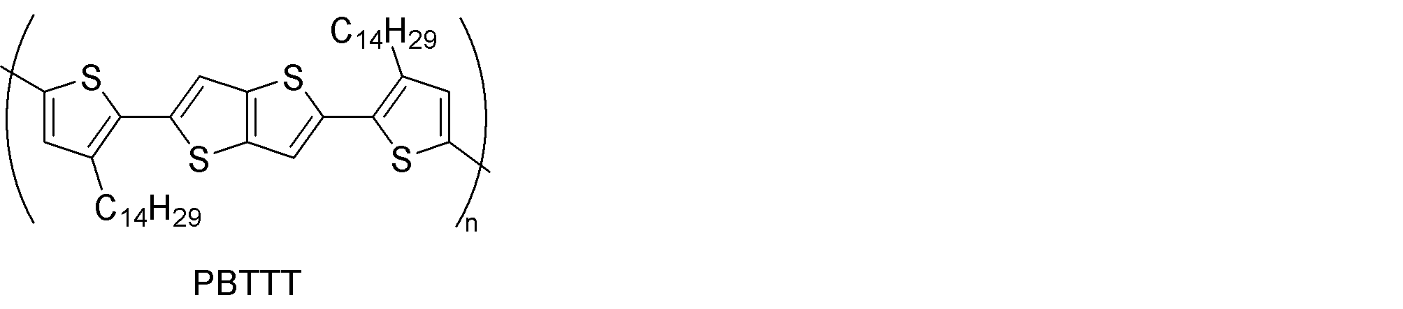
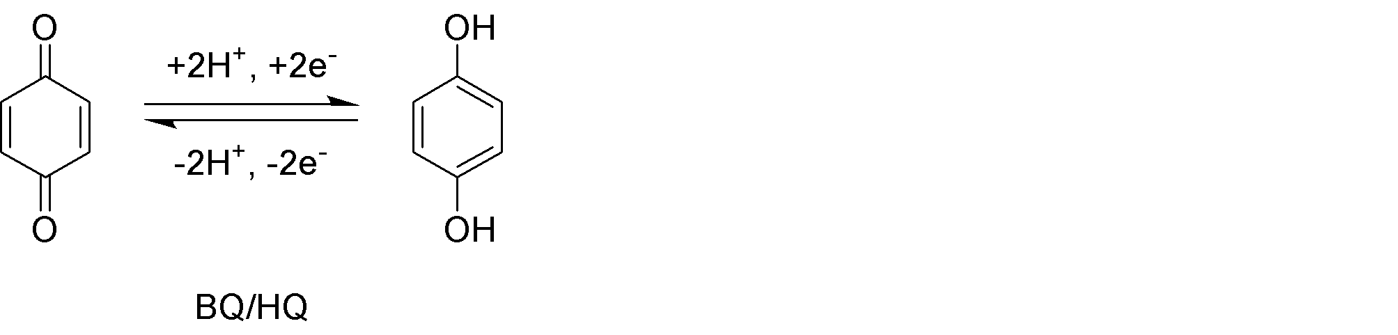
図1は、PBTTTと、BQ/HQのエネルギーダイアグラムである。縦軸は、真空準位を基準としたエネルギーを表している。BQ/HQのレドックスポテンシャルは、水溶液のpHを調整することで、容易に調整することができ、PBTTTとの関係では、プロトン移動を伴う電子移動(ET)を起こし得る関係となる。すなわち、BQ/HQがPBTTTに対して第3酸化剤として働き得る関係にある。
ドーピング工程では、図2(A)~図2(C)に示すメカニズムでドーピングが起こると考えられる。
まず、BQ/HQ及びドーパントアニオンY-と対カチオン(スペクテータイオン;図示せず)との塩が溶解されたドープ溶液と、PBTTT層とが接触すると、BQの少なくとも一部は、水溶液中から2つのプロトン、PBTTTから2つの電子の供与を受け、HQに還元される(図2(A))。一方、PBTTTは酸化され、すなわち、PBTTT層にキャリアであるホールが注入され、PBTTT層の表面が正に帯電する(図2(A))。
次に、静電的相互作用により、ドープ溶液中のドーパントイオンY-が、正に帯電した有機半導体層表面から導入される(図2(B))。その結果、PBTTT層の表面を含む領域には、ホールとドーパントイオンY-とが導入されたドープ層が形成される(図2(C))。
下記式は、上記のドーピング工程の各段階で生ずる反応のモデル的な反応式である。図2(A)の段階では、(i)の反応が起こる。図2(B)及び図2(C)の段階では、(ii)及び(iii)の反応が起こる。

上記推定メカニズムは、p型有機半導体層にホール及びドーパントアニオンが導入される態様に関するものである。n型有機半導体層に電子及びドーパントカチオンが導入される場合も、ドーピングの推定メカニズムは同様である。また、第3酸化剤としてk=2のBQを使用した例でドーピングの推定メカニズムを説明したが、kが2以外の場合も、ドーピングの推定メカニズムは同様である。
〔1-2-4.有機半導体層前駆体及び有機半導体層〕
ドーピング工程において、ドーピングに供される有機半導体層前駆体について説明する。
なお、本実施形態に係る製造方法がドーピング工程を含まない態様においては、「ドーピングに供される有機半導体層前駆体」は、そのまま「有機半導体層」として縦型ダイオードに組み込まれる層である。本開示では、「有機半導体層」を「有機半導体層前駆体」を含む概念として使用することがあり、「有機半導体層前駆体」を「有機半導体層」を含む概念として使用することがある。
ドーピング工程において、ドーピングに供される有機半導体層前駆体について説明する。
なお、本実施形態に係る製造方法がドーピング工程を含まない態様においては、「ドーピングに供される有機半導体層前駆体」は、そのまま「有機半導体層」として縦型ダイオードに組み込まれる層である。本開示では、「有機半導体層」を「有機半導体層前駆体」を含む概念として使用することがあり、「有機半導体層前駆体」を「有機半導体層」を含む概念として使用することがある。
有機半導体層前駆体は、有機半導体により形成された層であり、単層構造又は多層構造を有する。また、有機半導体層前駆体の層構造及び有機半導体層前駆体を構成する有機半導体の種類は、第1電極の表面修飾、ドーピング工程で有機半導体層前駆体に注入されるキャリア及びドーパントイオンの種類等に応じて適宜選択すればよい。
例えば、電極修飾工程において、第1電極に低分子疎水性カチオンを付着させた場合には、有機半導体層前駆体は、単層構造のn型有機半導体層前駆体としてもよく;第1電極から第2電極に向かってn型有機半導体層とp型有機半導体層とを積層した二層構造の有機半導体層前駆体としてもよく;第1電極から第2電極に向かってn型有機半導体層とi型有機半導体層とp型有機半導体層とを積層した三層構造の有機半導体層前駆体としてもよい。このとき、ドーピングが施される層がp型有機半導体層である場合は、p型有機半導体層にホール及びドーパントアニオンが注入されるよう、上述した二層構造又は三層構造の有機半導体層前駆体を採用することが好適である。電極修飾工程において、第1電極に低分子疎水性カチオンを付着させた場合も、上記のように、ダイオードの仕組みに基づいて好適な有機半導体層前駆体を選択すればよい。
有機半導体層前駆体を構成する有機半導体は、低分子化合物であってもよく、高分子化合物であってもよい。
p型低分子化合物としては、縮合多環化合物、トリアリールアミン化合物、ヘテロ5員環化合物、フタロシアニン化合物、ポルフィリン化合物、カーボンナノチューブ、及び、グラフェン等が挙げられる。
縮合多環化合物としては、例えば、アントラセン、テトラセン、ペンタセン、アントラジチオフェン、及びヘキサベンゾコロネン等が挙げられる。これらは、置換基を有していてもよい。
トリアリールアミン化合物としては、例えば、4,4’,4”-トリス[(3-メチルフェニル)フェニルアミノ]トリフェニルアミン(m-MTDATA)、4,4’,4”-トリス[2-ナフチル(フェニル)アミノ]トリフェニルアミン(2-TNATA)、N,N’-ジ(1-ナフチル)-N,N’-ジフェニル-(1,1’-ビフェニル)-4,4’-ジアミン(NPD)、N,N’-ジフェニル-N,N’-ジ(m-トリル)ベンジジン(TPD)、1,3-ビス(9-カルバゾリル)ベンゼン(mCP)、及び4,4’-ビス(9-カルバゾリル)-2,2’-ビフェニル(CBP)等が挙げられる。
ヘテロ5員環化合物としては、例えば、オリゴチオフェン及びテトラチアフルバレン(TTF)等が挙げられる。これらは、置換基を有していてもよい。
フタロシアニン化合物は、フタロシアニン、ナフタロシアニン、アントラシアニン、及びテトラピラジノポルフィラジン等の金属錯体が挙げられる。これらは、置換基を有していてもよい。
ポルフィリン化合物は、置換基を有していてもよいポルフィリンの金属錯体等が挙げられる。
p型低分子化合物としては、3,11-ジオクチルジナフ卜[2,3-d:2’,3’-d’]ベンゾ[1,2-b:4,5-b’]ジチオフェン(C8-DNBDT)、3,11-ジデシルジナフ卜[2,3-d:2’,3’-d’]ベンゾ[1,2-b:4,5-b’]ジチオフェン(C10-DNBDT)、3,9-ジヘキシルジナフト[2,3-b;2’,3-d]チオフェン(C6-DNT)、2,9-ジナフト[2,3-b:2’,3’-f]チエノ[3,2-b]チオフェン(C10-DNTT)、2,7-ジオクチルベンゾチエノ[3,2-b][1]ベンゾチオフェン(C8-BTBT)、及び6,13-ビス(トリイソプロピルシリルエチニル)ペンタセン等が好ましい。
n型低分子化合物としては、フラーレン化合物、電子欠乏性フタロシアニン化合物、縮合多環化合物(ナフタレンテトラカルボニル化合物及びペリレンテトラカルボニル化合物等)、TCNQ化合物(テトラシアノキノジメタン化合物)、及びグラフェン等が挙げられる。
フラーレン化合物としては、C60、C70、C76、C78、C80、C82、C84、C86、C88、C90、C96、C116、C180、C240、C540、及びPCBM等が挙げられ、好ましくはC60、C70、C86、又はPCBMである。これらは、置換基を有していてもよい。
電子欠乏性フタロシアニン化合物とは、フタロシアニン、ナフタロシアニン、アントラシアニン、及びテトラピラジノポルフィラジン等のフタロシアニン化合物に電子求引基が4つ以上結合したものの金属錯体が挙げられる。これらは、置換基を有していてもよい。
電子欠乏性フタロシアニン化合物としては、例えば、フッ素化フタロシアニン(F16MPc)及び塩素化フタロシアニン(Cl16MPc)等が挙げられる。なお、Mは中心金属を、Pcはフタロシアニンである。
電子欠乏性フタロシアニン化合物としては、例えば、フッ素化フタロシアニン(F16MPc)及び塩素化フタロシアニン(Cl16MPc)等が挙げられる。なお、Mは中心金属を、Pcはフタロシアニンである。
ナフタレンテトラカルボニル化合物としては、ナフタレンテトラカルボン酸無水物(NTCDA)、ナフタレンビスイミド化合物(NTCDI)、及びぺリノン顔料(Pigment Orange 43、Pigment Red 194等)が挙げられる。
ペリレンテトラカルボニル化合物としては、ペリレンテトラカルボン酸無水物(PTCDA)、ペリレンビスイミド化合物(PTCDI)、及びベンゾイミダゾール縮環体(PV)等が挙げられる。具体的なペリレンテトラカルボニル化合物としては、ジシアノペリレン-3,4:9,10-ビス(ジカルボキシイミド)等が挙げられる。
TCNQ化合物としては、のTCNQ、TCNQ、及びこれらの化合物のベンゼン環部分を別の芳香環やヘテロ環に置き換えたものが挙げられる。具体的なTCNQ化合物としては、TCNQ(テトラシアノキノジメタン)、TCNAQ(テトラシアノアントラキノジメタン)、及びTCN3T(2,2’-((2E,2”E)-3’,4’-アルキル置換-5H,5”H-[2,2’:5’,2”-ターチオフェン]-5,5”-ジイルジエン)ジマロノニトリル誘導体)等が挙げられる。
高分子化合物としては、π共役高分子が挙げられる。
π共役高分子としては、例えば、ポリチオフェン、ポリセレノフェン、ポリピロール、ポリパラフェニレン、ポリパラフェニレンビニレン、ポリチオフェンビニレン、及びポリアニリン等が挙げられる。これらは、置換基を有してもよい。
π共役高分子としては、例えば、ポリチオフェン、ポリセレノフェン、ポリピロール、ポリパラフェニレン、ポリパラフェニレンビニレン、ポリチオフェンビニレン、及びポリアニリン等が挙げられる。これらは、置換基を有してもよい。
p型高分子化合物としては、[ポリ[2,5-ビス(3-テトラデシルチオフェン-2-イル)チエノ[3,2-b]チオフェン]](PBTTT-C14)、ポリ[2,5-(2-オクチルドデシル)-3,6-ジケトピロロピロール-オルト-5,5-(2,5-ジ(チエ-2-イル)チエノ[3,2-b]チオフェン)](Poly[2,5-(2-octyldodecyl)-3,6-ジケトピロロピロール-alt-5,5-(2,5-ジ(チエン-2-イル)チエノ[3,2-b]チオフェン)](PDPP2T-TT-OD))、及びポリ[2,5-(2-オクチルドデシル)-3,6-ジケトピロロピロール-o-(ジ(チエノチエ-2-イル)チオフェン)](PDPP2TT-T)等が挙げられる。
n型高分子化合物としては、ポリ{[N,N’-ビス(2-オクチルドデシル)ナフタレン-1,4,5,8-ビス(ジカルボキシイミド)-2,6-ジイル]-o-5,5’-(2,2’-ビチオフェン)}(N2200)及び(ポリ{[N,N’-ビス(2-オクチルドデシル)ナフタレン-1,4,5,8-bis(ジカルボキシイミド)-2,6-ジイル]-alt-5,5’-(2,2’-ビチオフェン)}(P(NDI2OD-T2))等が挙げられる。
有機半導体は、1種単独で使用してもよく、2種以上を任意の比率及び組み合わせで併用してもよい。
有機半導体は、結晶化していてもよい。特に、有機半導体が低分子化合物である場合、有機半導体は、単結晶であることが好ましい。また、有機半導体が高分子化合物である場合は、この高分子化合物は、分子配向していてもよい。
有機半導体層前駆体の作製方法は、特に限定されず、公知の方法及びこれに準じた方法等の任意の方法を採用することができる。公知の方法としては、例えば、有機半導体及び溶媒を含む組成物を用いた塗布法により組成物層を形成し、組成物層から溶媒を除去して有機半導体層前駆体を得る方法が挙げられる。有機半導体層前駆体が多層構造を有する場合は、上述の組成物層の形成及び組成物層からの溶媒除去からなるサイクルを複数回繰り返すことにより、有機半導体層前駆体を作製することができる。
組成物に含まれる溶媒としては、有機半導体を溶解し得る限り特に限定されず、例えば、ジクロロベンゼン等の芳香族系有機溶媒;アセトニトリル;酢酸ブチル;及びフルオロアルコール;等が挙げられる。
組成物中における有機半導体の含有量は、目的とする有機半導体層前駆体の厚さに応じて適宜調整すればよく、好ましくは0.1質量%以上99質量%以下である。
組成物中における有機半導体の含有量は、目的とする有機半導体層前駆体の厚さに応じて適宜調整すればよく、好ましくは0.1質量%以上99質量%以下である。
この他、公知の方法としては、国際公開第2020/085342号の段落0025~段落0033に記載された方法;特開2020-38133号公報の段落0026~段落0029に記載された方法;も挙げられる。
有機半導体層前駆体の厚さ(有機半導体層前駆体が多層構造の場合は、総厚)は、特に限定されず、縦型ダイオードの用途及び素子寿命等を勘案して適宜調整すればよい。有機半導体層前駆体の具体的な厚さとしては、例えば、11nm以上300nm以下が挙げられ、好ましくは12nm以上70nm以下、より好ましくは15nm以上50nm以下、さらにより好ましくは18nm以上40nm以下、特に好ましくは20nm以上30nm以下である。なお、本実施形態に係る製造方法がドーピング工程を含まない態様においては、ここでいう「有機半導体層前駆体」は、ドープされて又はそのまま「有機半導体層」として縦型ダイオードに組み込まれる層であるため、有機半導体の総厚さも上述の通りである。
本実施形態では、整流特性の向上に寄与するイオン層が、有機半導体層中に分散しているのではなく、第1電極と有機半導体層との界面に存在するため、ドープ層の有無にかかわらず、有機半導体層の厚さが小さい場合であっても高い整流比を実現し得る。より具体的には、従来の縦型ダイオードの有機半導体層の一般的な厚さが100nm程度であるところ、後述する実施例では、有機半導体層の厚さが25nmであるにもかかわらず、良好な整流特性を示す縦型ダイオードが得られている。
〔1-3.積層工程〕
本実施形態では、第1電極、有機半導体層、及び第2電極は、この順に隣接して積層される。このとき、第1電極と有機半導体層とは、電極修飾工程で修飾された第1電極の表面と有機半導体層とが接触するよう積層される。
また、ドーピング工程により有機半導体層にドープ層が形成されている場合には、有機半導体層と第2電極とは、ドープ層と第2電極とが接触するよう積層される。
本実施形態では、第1電極、有機半導体層、及び第2電極は、この順に隣接して積層される。このとき、第1電極と有機半導体層とは、電極修飾工程で修飾された第1電極の表面と有機半導体層とが接触するよう積層される。
また、ドーピング工程により有機半導体層にドープ層が形成されている場合には、有機半導体層と第2電極とは、ドープ層と第2電極とが接触するよう積層される。
各層の積層は、各層が上述した条件を満たす順に積層されるよう行われる限り、その方法は特に限定されず、公知の方法及びこれに準じた方法等の任意の方法を採用し得る。
例えば、第1電極を作製し、第1電極の表面を修飾し、表面修飾された第1電極上に有機半導体層を作製し、有機半導体層の上に第2電極を作製することにより積層を行ってもよく、第2電極を作製し、第2電極上に有機半導体層を作製し、有機半導体層の上に表面修飾された第1電極を配置することにより積層を行ってもよい。有機半導体層を作製する方法としては、例えば上記〔1-2-4.有機半導体層前駆体及び有機半導体層〕の項目で述べた湿式法等が挙げられる。また、有機半導体層の積層は、有機半導体層を転写基板上に作製し、この有機半導体層を表面が修飾された第1電極及び第2電極のうち一方の電極上に転写し、有機半導体層の上に他方の電極を作製する転写法により行ってもよい。
本実施形態に係る製造方法が、ドーピング工程を含む場合は、例えば、第1電極を作製し、第1電極の表面を修飾し、表面修飾された第1電極上に有機半導体層前駆体を作製し、有機半導体層前駆体をドーピング工程に供し、ドーピング工程により形成されたドープ層上に第2電極を作製することにより積層を行ってもよく、第2電極を作製し、ドーピング工程によりドープ層が形成されている有機半導体層を転写基板から第2電極上に転写し、有機半導体層のアンドープ層の上に表面修飾された第1電極を配置することにより積層を行ってもよい。
〔1-3-1.第2電極〕
以下、有機半導体層とともに積層する第2電極の材料及び第2電極を作製する方法について説明する。
第2電極は、第1電極がカソードである場合はアノードであり、第1電極がアノードである場合はカソードである。
以下、有機半導体層とともに積層する第2電極の材料及び第2電極を作製する方法について説明する。
第2電極は、第1電極がカソードである場合はアノードであり、第1電極がアノードである場合はカソードである。
上記〔1-1-2.第1電極〕の項目で述べたように、第2電極がアノードである場合、第2電極は、有機半導体層を構成する有機半導体及び第1電極より大きい仕事関数を示すことが望ましい。また、第2電極がカソードである場合、第2電極は、有機半導体のLUMOより小さい仕事関数を有し、かつ、第1電極よりも小さい仕事関数を有することが望ましい。
第2電極を構成する材料は、特に限定されず、第1電極及び有機半導体の種類に応じて導電性材料から適宜選択すればよい。具体的な電極材料としては、未修飾の第1電極を構成する材料として例示したものが挙げられる。
第2電極の厚さは、特に限定されず、縦型ダイオードの用途及び素子寿命等を勘案して適宜調整すればよい。第2電極の具体的な厚さとしては、例えば、10nm以上200nm以下が挙げられ、好ましくは20nm以上50nm以下である。
第2電極は、公知の方法及びこれに準じた方法等の任意の方法により、所定の厚さとなるよう作製され、他の層とともに積層される。第2電極を作製するための公知の方法としては、例えば、真空蒸着法、スパッタリング、化学蒸着法、及びメッキ法等が挙げられる。
第1電極の上に他の層を積層する場合、第1電極は、基板上に形成されたものであることが好ましく、第2電極の上に他の層を積層する場合も同様である。
基板は、第1電極又は第2電極を形成することができる限り、特に限定されないが、有機半導体層を構成する有機半導体と化学的に反応しないものであることが好ましい。このような基板としては、例えば、ガラス基板及びシリコン基板等が挙げられる。
〔1-4.他の工程〕
本実施形態に係る製造方法は、上記工程以外の他の工程を含んでいてもよい。
他の工程としては、例えば、電極修飾工程の後に、表面が修飾された第1電極を洗浄する工程;及びドーピング工程の後に、ドーピングされた有機半導体層を洗浄する工程;等が挙げられる。
本実施形態に係る製造方法は、上記工程以外の他の工程を含んでいてもよい。
他の工程としては、例えば、電極修飾工程の後に、表面が修飾された第1電極を洗浄する工程;及びドーピング工程の後に、ドーピングされた有機半導体層を洗浄する工程;等が挙げられる。
或いは、本実施形態に係る製造方法は、上記ドーピング工程とともに、又はドーピング工程に代えて、国際公開第2020/085342号等に開示されているような公知の方法及びこれに準じた方法等の任意の方法により有機半導体層のドーピングを行う工程を含んでいてもよい。
〔2.縦型ダイオード〕
本開示の第2実施形態は、第1電極、有機半導体層、及び第2電極がこの順に隣接して積層された縦型ダイオードであって、前記第1電極の表面であって前記有機半導体層と隣接する面に低分子疎水性イオンが付着している縦型ダイオードである。本実施形態に係る縦型ダイオードは、上記第1実施形態に係る製造方法により製造することができる。また、本実施形態に係る縦型ダイオードは、整流特性に優れ、したがって、整流ダイオードとして好適に使用し得る。
本開示の第2実施形態は、第1電極、有機半導体層、及び第2電極がこの順に隣接して積層された縦型ダイオードであって、前記第1電極の表面であって前記有機半導体層と隣接する面に低分子疎水性イオンが付着している縦型ダイオードである。本実施形態に係る縦型ダイオードは、上記第1実施形態に係る製造方法により製造することができる。また、本実施形態に係る縦型ダイオードは、整流特性に優れ、したがって、整流ダイオードとして好適に使用し得る。
図4(A)に示すように、本実施形態に係る縦型ダイオード10は、第1電極12、有機半導体層14、及び第2電極18がこの順に隣接して積層された縦型ダイオードである。前記第1電極12の表面であって前記有機半導体層14と隣接する面には、低分子疎水性イオン13が付着している。
低分子疎水性イオンは、第1実施形態における電極修飾工程により第1電極の表面に静電的に付着したものである。すなわち、低分子疎水性イオンは、表面修飾液(S1)に含まれる第1還元剤由来の低分子疎水性カチオン及び/又は他の低分子疎水性カチオン;表面修飾液(S2)に含まれる第1酸化剤由来の低分子疎水性アニオン及び/又は他の低分子疎水性アニオン;表面修飾液(S3)に含まれる低分子疎水性閉殻カチオン;並びに表面修飾液(S4)に含まれる低分子疎水性閉殻アニオン;のいずれかである。したがって、低分子疎水性イオンについては、〔1-1-1.表面修飾液〕の項目における説明をここに援用する。
縦型ダイオードにおいて、低分子疎水性イオン被覆率は、好ましくは10面積%以上50面積%以下、より好ましくは15面積%以上40面積%以下、さらに好ましくは20面積%以上30面積%以下である。低分子疎水性イオン被覆率が上記範囲内であることにより、表面修飾前と比べて仕事関数が大幅にシフトした第1電極が得られ、大気雰囲気下であっても、そのシフトした仕事関数を維持することができる。
なお、第1電極の表面修飾を行った後、縦型ダイオードを製造する過程又は縦型ダイオードの保管中に、第1電極の表面に付着した分子疎水性イオンの一部が有機半導体層中に拡散する場合があるが、第1電極の表面修飾直後、及び縦型ダイオード製造後のいずれにおいても、低分子疎水性イオン被覆率の好ましい範囲は、上記の通りである。
低分子疎水性イオン被覆率は、X線光電子分光法(XPS)により測定することができる。電極由来の原子に由来するスペクトル強度と低分子疎水性イオンの原子に由来するスペクトル強度を分析することにより、被覆率、及び低分子疎水性イオン層の膜厚を求めることが可能である。
また、上述したように、本実施形態では、第1電極表面上での低分子疎水性イオンと対イオンとの塩の形成が抑制されている。低分子疎水性イオンは、対イオンの中でも、有機半導体層を構成する有機半導体に由来するイオン、プロトン、水酸化物イオン、及び前記第1電極に含まれる金属のイオンのいずれとも塩を形成しないことが好ましい。
より具体的には、第1電極の表面であって有機半導体層と隣接する面に付着している低分子疎水性イオンのうち、対イオンと塩を形成している低分子疎水性イオンの割合は、好ましくは0mol%以上25mol%以下、より好ましくは0mol%超20mol%以下、さらに好ましくは0mol%以上15mol%以下、特に好ましくは5mol%以上10mol%以下である。
第1電極の表面上で、対イオンと塩を形成している低分子疎水性イオンの割合は、X線光電子分光法(XPS)により測定することができる。対イオンの原子に由来するスペクトル強度と低分子疎水性イオンの原子に由来するスペクトル強度を分析することにより、低分子疎水性イオンのうち塩を形成している割合を評価することが可能である。
図4(B)に示すように、本実施形態に係る縦型ダイオード10は、有機半導体層14が、ドープ層17とアンドープ層15とを有することが好ましい。ドープ層17は、有機半導体層14の最外層として形成される層であって、第2電極18と隣接する層である。このドープ層17は、第1実施形態におけるドーピング工程において、有機半導体層前駆体にキャリア(電子又はホール)とドーパントイオンとが注入されることで形成された層である。なお、本実施形態において、有機半導体層は、ドープ層とアンドープ層とからなることが好ましい。また、アンドープ層は、単層構造を有していてもよく、多層構造を有していてもよい。
ドープ層に含まれるドーパントイオンは、ドープ溶液に含まれるドーパントイオンの塩に由来するものであって、キャリアとは逆の極性を有する。したがって、ドープ層に含まれるキャリアがホールである場合は、ドープ層に含まれるドーパントイオンはドーパントアニオンである。有機半導体層がこのようなドープ層を有する場合、縦型ダイオードの整流特性が向上する点及び低電圧における電流密度が向上する点で、第1電極の表面を修飾する低分子疎水性イオンは、低分子疎水性カチオンであることが好ましい。
一方、ドープ層に含まれるキャリアが電子である場合は、ドープ層に含まれるドーパントイオンはドーパントカチオンである。有機半導体層がこのようなドープ層を有する場合、縦型ダイオードの整流特性が向上する点及び低電圧における電流密度が向上する点で、第1電極の表面を修飾する低分子疎水性イオンは、低分子疎水性アニオンであることが好ましい。
ドープ層を構成する有機半導体としてホール輸送性有機半導体の層、すなわち、p型有機半導体の層を用いる場合、ドープ層にホール及びドーパントアニオンが注入されていることにより、整流特性に優れ、低電圧における電流密度の高い縦型ダイオードを得ることができる。一方、ドープ層を構成する有機半導体として電子輸送性有機半導体の層、すなわち、n型有機半導体の層を用いる場合、ドープ層に電子及びドーパントカチオンが注入されていることにより、整流特性に優れ、低電圧における電流密度の高い縦型ダイオードを得ることができる。
ドープ層に含まれるドーパントイオンは、対イオンと塩を形成しないことが好ましく、対イオンの中でも、有機半導体層を構成する有機半導体に由来するイオン、プロトン、水酸化物イオン、第1電極に含まれる金属のイオン、及び第2電極に含まれる金属のイオン以外の対イオンのいずれとも塩を形成しないことがより好ましい。
より具体的には、ドープ層に含まれるドーパントイオンのうち、有機半導体層を構成する有機半導体に由来するイオン、プロトン、水酸化物イオン、第1電極に含まれる金属のイオン、又は第2電極に含まれる金属のイオン以外の対イオンと塩を形成しているドーパントイオンの割合は、好ましくは0mol%以上25mol%以下、より好ましくは0mol%超20mol%以下、さらに好ましくは0mol%以上15mol%以下、特に好ましくは5mol%以上10mol%以下である。
対イオンと塩を形成しているドーパントイオンの割合は、X線光電子分光法(XPS)により測定することができる。
本実施形態において、有機半導体層前駆体中、ドープ溶液と接触した有機半導体層前駆体の表面からキャリア及びドーパントイオンが到達した深さまでの領域がドープ層となり、その余がアンドープ層となる。なお、キャリア及びドーパントイオンが到達した深さは、通常、ドープ層の厚さTdに相当する。
ドープ層の厚さTdは、特に限定されないが、好ましくは1nm以上100nm以下、より好ましくは2nm以上20nm以下、さらに好ましくは3nm以上15nm以下、さらにより好ましくは4nm以上10nm以下である。また、ドープ層の厚さTdを有機半導体層の総厚Toから差し引いたアンドープ層の厚さTuは、好ましくは10nm以上200nm以下、より好ましくは10nm以上50nm以下、さらに好ましくは12nm以上30nm以下、さらにより好ましくは15nm以上25nm以下である。ドープ層の厚さTdを上記範囲内とすることにより、整流性を保ちながら順方向に流れる電流値を大きくすることが可能となる。
アンドープ層Tuの厚さはキャパシタンス測定により推定することが可能であり、接触段差計によりアンドープ層Tuの厚さを求められれば、ドープ層の厚さも推定することが可能である。
アンドープ層は、第1実施形態におけるドーピング工程でキャリア及びドーパントイオンが注入されていない層である。ただし、ドーピング工程後の製造工程及び縦型ダイオードの保管中等に、ドープ層中のドーパントイオンが当該領域中に拡散する場合もあるため、本開示において、キャパシタンス測定において抵抗成分として振る舞う層を「ドープ層」、容量成分として振る舞う層を「アンドープ層」と呼ぶものとする。また、図4(B)中、アンドープ層15は、1つの層として図示されているが、アンドープ層は多層構造を有していてもよい。
本実施形態に係る縦型ダイオードは、高周波の交流電力を直流電力に効率よく変換することができる。本開示において、「高周波」とは、10MHz以上の周波数(例えば、10MHz、100MHz又は1GHz)を意味する。
より具体的には、本実施形態に係る縦型ダイオードは、10HMzの交流電力を直流電力に変換する変換効率(交流-直流変換効率)が4%以上であることが好ましく、5%以上であることがより好ましく、5%超であることがさらに好ましい。
或いは、本実施形態に係る縦型ダイオードは、1GMzの交流電力を直流電力に変換する変換効率(交流-直流変換効率)が4%以上であることが好ましく、5%以上であることがより好ましく、5%超であることがさらに好ましい。
或いは、本実施形態に係る縦型ダイオードは、1GMzの交流電力を直流電力に変換する変換効率(交流-直流変換効率)が4%以上であることが好ましく、5%以上であることがより好ましく、5%超であることがさらに好ましい。
本実施形態に係る縦型ダイオードであって、第1電極の表面に低分子疎水性カチオンが付着している縦型ダイオードの具体的な層構造としては、例えば、下記(A1)~(A5)で表される層構造が好ましく挙げられる。なお、下記(A1)~(A5)には記載していないが、図4(A)及び図4(B)に示すように、第1電極又は第2電極は、通常基板11の上に形成されている。
(A1)第1電極/n型有機半導体層/第2電極
(A2)第1電極/n型有機半導体層/p型有機半導体層/第2電極
(A3)第1電極/n型有機半導体層/p型有機半導体層(ドープ層)/第2電極
(A4)第1電極/n型有機半導体層/i型有機半導体層/p型有機半導体層/第2電極(A5)第1電極/n型有機半導体層/i型有機半導体層/p型有機半導体層(ドープ層)/第2電極
(A2)第1電極/n型有機半導体層/p型有機半導体層/第2電極
(A3)第1電極/n型有機半導体層/p型有機半導体層(ドープ層)/第2電極
(A4)第1電極/n型有機半導体層/i型有機半導体層/p型有機半導体層/第2電極(A5)第1電極/n型有機半導体層/i型有機半導体層/p型有機半導体層(ドープ層)/第2電極
本実施形態に係る縦型ダイオードであって、第1電極の表面に低分子疎水性アニオンが付着している縦型ダイオードの具体的な層構造としては、例えば、下記(A6)~(A10)で表される層構造が好ましく挙げられる。なお、下記(A6)~(A10)には記載していないが、第1電極又は第2電極は、通常基板上に形成されている。
(A6)第1電極/p型有機半導体層/第2電極
(A7)第1電極/p型有機半導体層/n型有機半導体層/第2電極
(A8)第1電極/p型有機半導体層/n型有機半導体層(ドープ層)/第2電極
(A9)第1電極/p型有機半導体層/i型有機半導体層/n型有機半導体層/第2電極(A10)第1電極/p型有機半導体層/i型有機半導体層/n型有機半導体層(ドープ層)/第2電極
(A7)第1電極/p型有機半導体層/n型有機半導体層/第2電極
(A8)第1電極/p型有機半導体層/n型有機半導体層(ドープ層)/第2電極
(A9)第1電極/p型有機半導体層/i型有機半導体層/n型有機半導体層/第2電極(A10)第1電極/p型有機半導体層/i型有機半導体層/n型有機半導体層(ドープ層)/第2電極
(A1)~(A10)中、「/」は、その前後に記載された層同士が互いに隣接することを意味する。
(A1)~(A5)中、「p型有機半導体層(ドープ層)」は、p型有機半導体層がホール及びドーパントアニオンを含むドープ層であるか、p型有機半導体層の一方の最外層がホール及びドーパントアニオンを含むドープ層であり、2電極と隣接していることを意味する。
(A6)~(A10)中、「n型有機半導体層(ドープ層)」は、n型有機半導体層が電子及びドーパントカチオンを含むドープ層であるか、n型有機半導体層の一方の最外層が電子及びドーパントカチオンを含むドープ層であり、2電極と隣接していることを意味する。
〔3.縦型ダイオードの製造方法〕
本開示の第3実施形態は、第1電極、ドープ層とアンドープ層とを有する有機半導体層、及び第2電極がこの順に隣接して、かつ、前記ドープ層が前記第1電極又は前記第2電極に隣接して積層された縦型ダイオードの製造方法であって、第4酸化剤又は第4還元剤及びドーパントイオンの塩を含む水溶液(以下、「ドープ溶液」と称することがある。)と、有機半導体層前駆体の表面とを接触させることで、前記ドープ層を形成するドーピング工程を含む。
本開示の第3実施形態は、第1電極、ドープ層とアンドープ層とを有する有機半導体層、及び第2電極がこの順に隣接して、かつ、前記ドープ層が前記第1電極又は前記第2電極に隣接して積層された縦型ダイオードの製造方法であって、第4酸化剤又は第4還元剤及びドーパントイオンの塩を含む水溶液(以下、「ドープ溶液」と称することがある。)と、有機半導体層前駆体の表面とを接触させることで、前記ドープ層を形成するドーピング工程を含む。
本実施形態によれば、第1電極又は第2電極の近傍にキャリア及びドーパントイオンが注入されたドープ層が形成される。これにより、ドープ層に隣接する電極から有機半導体層へのキャリア注入性が向上するため、優れた整流特性を示す縦型ダイオードを得ることができる。したがって、本実施形態に係る製造方法は、整流ダイオードを製造する方法として有用である。また、本実施形態の好適な態様によれば、高周波応答性に優れた縦型ダイオード又は低電圧でも高い電流密度を示す縦型ダイオードを得ることができる。
〔3-1.ドーピング工程〕
ドーピング工程は、有機半導体層の最外層としてドープ層を形成する工程であり、ドープ層とアンドープ層とを有する有機半導体層を作製する工程(以下、「有機半導体層作製工程」と称することがある。)の一工程である。なお、本実施形態において、有機半導体層は、ドープ層とアンドープ層とからなることが好ましい。また、アンドープ層は、単層構造を有していてもよく、多層構造を有していてもよい。
ドーピング工程は、有機半導体層の最外層としてドープ層を形成する工程であり、ドープ層とアンドープ層とを有する有機半導体層を作製する工程(以下、「有機半導体層作製工程」と称することがある。)の一工程である。なお、本実施形態において、有機半導体層は、ドープ層とアンドープ層とからなることが好ましい。また、アンドープ層は、単層構造を有していてもよく、多層構造を有していてもよい。
有機半導体層作製工程は、有機半導体層前駆体をドーピング工程に供し、有機半導体層前駆体の表面から所望の深さまでの領域にキャリア及びドーパントイオンを注入することにより、ドープ層とアンドープ層を有する有機半導体層を得る工程A;又は有機半導体層前駆体をドーピング工程に供し、有機半導体層前駆体全体にキャリア及びドーパントイオンを注入することでドープ層を形成し、得られたドープ層にアンドープ有機半導体層を積層することにより、有機半導体層を得る工程B;である。
工程Aにおけるドーピング工程は、第1実施形態におけるドーピング工程と同プロセスであり、その好ましい態様も同様であるため、〔1-2.ドーピング工程〕の項目における説明をここに援用する。このとき、〔1-2.ドーピング工程〕の項目中、第3酸化剤及び第3還元剤は、それぞれ、第4酸化剤及び第4還元剤と読み替えるものとする。
工程Aにおいては、通常、有機半導体層前駆体中、ドープ溶液と接触した有機半導体層前駆体の表面からキャリア及びドーパントイオンが到達した深さまでの領域がドープ層となり、その余がアンドープ層となる。なお、キャリア及びドーパントイオンを注入する「所望の深さ」は、通常、後述するドープ層の厚さTdに相当するものである。
工程Bにおけるドーピング工程は、有機半導体層前駆体の一部でなく全体にキャリア及びドーパントイオンが注入される点以外は、第1実施形態におけるドーピング工程と同プロセスである。したがって、〔1-2.ドーピング工程〕の項目における説明をここに援用するが、有機半導体層前駆体全体にキャリア及びドーパントイオンを注入するための方法については、以下に述べる通りである。なお、〔1-2.ドーピング工程〕の項目中、第3酸化剤及び第3還元剤は、それぞれ、第4酸化剤及び第4還元剤と読み替えるものとする。
有機半導体層前駆体全体へのキャリア及びドーパントイオンの注入は、有機半導体層前駆体の厚さを、ドープ層に相当する厚さに設定することによって達成できるが、ドープ溶液中の第4酸化剤又は第4還元剤の総含有量の調整;有機半導体層前駆体とドープ溶液との接触温度の調整;及び有機半導体層前駆体とドープ溶液との接触時間の調整;のうち1以上を組み合わせることにより、より効率的に達成することができる。これらの条件の調整は、〔1-2.ドーピング工程〕で述べた範囲内で行うことが好ましい。
工程Bにおいて、有機半導体層前駆体及びアンドープ層は、公知の方法及びこれに準じた方法等の任意の方法により作製することができる。公知の方法としては、例えば上記〔1-2-4.有機半導体層前駆体及び有機半導体層〕の項目で述べた湿式法等が挙げられる。また、後述するように、有機半導体層前駆体は、第1電極又は第2電極の直上に作製され、その後ドーピング工程に供されることが好ましい。
本開示において、工程Aでキャリア及びドーパントイオンを注入する「所望の深さ」は、通常、後述するドープ層の厚さTdに相当する。また、工程Bでドーピング工程により形成されるドープ層の厚さは、通常、後述するドープ層の厚さTdに相当する。
〔3-2.電極修飾工程〕
ドープ層が第2電極に隣接する層である場合、本実施形態に係る製造方法は、第1電極の表面と表面修飾液とを接触させることにより、第1電極の表面を修飾する電極修飾工程を含むことが好ましい。電極修飾工程で用いる表面修飾液は、表面修飾液(S1)~表面修飾液(S4)のいずれかである。
(S1)第1電極を還元するとともに低分子疎水性カチオンを生じる第1還元剤を含む表面修飾液。
(S2)第1電極を酸化するとともに低分子疎水性アニオンを生じる第1酸化剤を含む表面修飾液。
(S3)第1電極を還元する第2還元剤と低分子疎水性閉殻カチオンとを含む表面修飾液。
(S4)第1電極を酸化する第2酸化剤と低分子疎水性閉殻アニオンとを含む表面修飾液。
ドープ層が第2電極に隣接する層である場合、本実施形態に係る製造方法は、第1電極の表面と表面修飾液とを接触させることにより、第1電極の表面を修飾する電極修飾工程を含むことが好ましい。電極修飾工程で用いる表面修飾液は、表面修飾液(S1)~表面修飾液(S4)のいずれかである。
(S1)第1電極を還元するとともに低分子疎水性カチオンを生じる第1還元剤を含む表面修飾液。
(S2)第1電極を酸化するとともに低分子疎水性アニオンを生じる第1酸化剤を含む表面修飾液。
(S3)第1電極を還元する第2還元剤と低分子疎水性閉殻カチオンとを含む表面修飾液。
(S4)第1電極を酸化する第2酸化剤と低分子疎水性閉殻アニオンとを含む表面修飾液。
本工程により、表面修飾された第1電極が得られる。表面修飾された第1電極は、第1還元剤又は第1酸化剤から生じた低分子疎水性イオンが第1電極の表面に付着したものである。
本実施形態における電極修飾工程は、第1実施形態における電極修飾工程と同プロセスであり、その好ましい態様も同様である。したがって、〔1-1.電極修飾工程〕の項目における説明をここに援用する。
ドーピング工程において、第4酸化剤及びドーパントアニオンの塩を含むドープ溶液を用いてドープ層を形成した場合、第2電極の近傍にホール及びドーパントアニオンが注入されたドープ層を有する縦型ダイオードが得られる。そのため、電極修飾工程では、表面修飾液(S1)又は(S3)を用いることで、電子が注入され、かつ、低分子疎水性カチオンが表面に静電的に付着した第1電極を作製することが好ましい。これにより、第2電極から有機半導体層へのホール注入性だけでなく、第1電極から有機半導体層への電子注入性が向上し、縦型ダイオードの整流特性及び低電圧における電流密度を向上し得るからである。
ドーピング工程において、第4還元剤及びドーパントカチオンの塩を含むドープ溶液を用いてドープ層を形成した場合、第2電極の近傍に電子及びドーパントカチオンが注入されたドープ層を有する縦型ダイオードが得られる。そのため、電極修飾工程では、表面修飾液(S2)又は(S4)を用いることで、ホールが注入され、かつ、疎水性閉殻アニオンが表面に静電的に付着した第1電極を作製することが好ましい。第2電極から有機半導体層への電子注入性だけでなく、第1電極から有機半導体層へのホール注入性が向上し、縦型ダイオードの整流特性及び低電圧における電流密度を向上し得るからである。
〔3-3.積層工程〕
本実施形態において、第1電極、ドープ層とアンドープ層を有する有機半導体層、及び第2電極は、この順に隣接して積層される。このとき、有機半導体層と第1電極又は第2電極とは、ドープ層と第1電極又は第2電極とが接触するよう積層される。
さらに、電極修飾工程により第1電極の表面を修飾した場合、第1電極と有機半導体層とは、第1電極の修飾された表面と有機半導体層とが接触するよう積層される。
本実施形態において、第1電極、ドープ層とアンドープ層を有する有機半導体層、及び第2電極は、この順に隣接して積層される。このとき、有機半導体層と第1電極又は第2電極とは、ドープ層と第1電極又は第2電極とが接触するよう積層される。
さらに、電極修飾工程により第1電極の表面を修飾した場合、第1電極と有機半導体層とは、第1電極の修飾された表面と有機半導体層とが接触するよう積層される。
各層の積層は、各層が上述した条件を満たす順に積層されるよう行われる限り、その方法は特に限定されず、公知の方法及びこれに準じた方法等の任意の方法を採用し得る。
例えば、有機半導体層作製工程が工程Aである場合は、第1電極を作製し、第1電極上に有機半導体層前駆体を作製し、有機半導体層前駆体をドーピング工程に供し、ドーピング工程により形成されたドープ層上に第2電極を作製することにより積層を行ってもよく、第2電極を作製し、第2電極上に有機半導体層前駆体を作製し、有機半導体層前駆体をドーピング工程に供し、ドーピング工程により形成されたドープ層上に第1電極を作製することにより積層を行ってもよい。或いは、有機半導体層作製工程により有機半導体層を転写基板上に作製し、この有機半導体層を第1電極及び第2電極のうち一方の電極上に転写し、有機半導体層の上に他方の電極を作製する転写法により各層を積層してもよい。
また、例えば、有機半導体層作製工程が工程Bである場合は、第1電極を作製し、第1電極上に有機半導体層前駆体を作製し、有機半導体層前駆体をドーピング工程に供し、ドーピング工程により形成されたドープ層上にアンドープ層を作製し、アンドープ層上に第2電極を作製することにより積層を行ってもよく、第2電極を作製し、第2電極上に有機半導体層前駆体を作製し、有機半導体層前駆体をドーピング工程に供し、ドーピング工程により形成されたドープ層上にアンドープ層を作製し、アンドープ層上に第2電極を作製することにより積層を行ってもよい。有機半導体層は、上記と同様に、転写法により第1電極及び第2電極と積層してもよいが、有機半導体層と第1電極又は第2電極との密着性を担保する観点から、第1電極又は第2電極の直上に有機半導体層前駆体を形成し、その後有機半導体層前駆体をドーピング工程に供することで電極上に積層されることが好ましい。
以下、有機半導体層とともに積層する第1電極及び第2電極の材料、並びに第1電極及び第2電極を作製する方法について説明する。
第1電極と第2電極とは、1対の電極である。すなわち、第1電極がカソードである場合、第2電極はアノードであり、第1電極がアノードである場合、第2電極はカソードである。
縦型ダイオードにおいて良好な整流特性を得るためには、一般的に、カソードは、隣接する有機半導体層を構成する有機半導体のLUMOよりも小さい仕事関数を有し、かつ、アノードより小さい仕事関数を有することが望ましい。また、アノードは、当該有機半導体のLUMOより大きい仕事関数を有することも望ましい。
したがって、第1電極及び2電極を構成する材料は、対となる電極の仕事関数及び有機半導体のLUMOの仕事関数に応じて導電性材料から適宜選択することが好ましい。本実施形態に係る製造方法が電極修飾工程を含む場合、電極材料の選択のために考慮する第1電極の仕事関数としては、第1電極表面修飾後の第1電極の仕事関数が採用される。
第1電極及び第2電極を構成する材料の具体例としては、例えば、白金、金、銀、アルミニウム、クロム、ニッケル、銅、チタン、マグネシウム、モリブデン、及びタングステン等の金属;これらの金属のうち2種以上を含む合金;並びに酸化インジウム、酸化スズ、酸化亜鉛、インジウムスズ酸化物(ITO)、及びインジウム亜鉛酸化物(IZO)等の金属酸化物;等が挙げられ、好ましくは金である。
第1電極及び第2電極は、公知の方法及びこれに準じた方法等の任意の方法により、所定の厚さとなるよう作製され、他の層とともに積層される。第1電極及び第2電極を作製するための公知の方法としては、例えば、真空蒸着法、スパッタリング、化学蒸着法、及びメッキ法等が挙げられる。
第1電極の厚さ及び2電極の厚さは、特に限定されず、縦型ダイオードの用途及び素子寿命等を勘案して適宜調整すればよい。これらの電極の具体的な厚さとしては、例えば、10nm以上200nm以下が挙げられ、好ましくは20nm以上50nm以下である。
第1電極の上に他の層を積層する場合、第1電極は、基板上に形成されたものであることが好ましく、第2電極の上に他の層を積層する場合も同様である。
基板は、第1電極又は第2電極を形成することができる限り、特に限定されないが、有機半導体層を構成する有機半導体と化学的に反応しないものであることが好ましい。このような基板としては、例えば、ガラス基板及びシリコン基板等が挙げられる。
基板は、第1電極又は第2電極を形成することができる限り、特に限定されないが、有機半導体層を構成する有機半導体と化学的に反応しないものであることが好ましい。このような基板としては、例えば、ガラス基板及びシリコン基板等が挙げられる。
〔3-4.他の工程〕
本実施形態に係る製造方法は、上記工程以外の他の工程を含んでいてもよい。
他の工程としては、例えば、ドーピング工程後に有機半導体層を洗浄する工程;及び表面が修飾された第1電極を洗浄する工程;等が挙げられる。
本実施形態に係る製造方法は、上記工程以外の他の工程を含んでいてもよい。
他の工程としては、例えば、ドーピング工程後に有機半導体層を洗浄する工程;及び表面が修飾された第1電極を洗浄する工程;等が挙げられる。
〔4.縦型ダイオード〕
本開示の第4実施形態は、第1電極、ドープ層とアンドープ層とを有する有機半導体層、及び第2電極がこの順に隣接して、かつ、前記ドープ層が前記第1電極又は前記第2電極に隣接して積層された縦型ダイオードである。前記ドープ層は、キャリア及びドーパントイオンを含み、前記ドーパントイオンは、疎水性閉殻イオンである。本実施形態に係る縦型ダイオードは、上記第3実施形態に係る製造方法により製造することができる。また、本実施形態に係る縦型ダイオードは、整流特性に優れ、したがって、整流ダイオードとして好適に使用し得る。
本開示の第4実施形態は、第1電極、ドープ層とアンドープ層とを有する有機半導体層、及び第2電極がこの順に隣接して、かつ、前記ドープ層が前記第1電極又は前記第2電極に隣接して積層された縦型ダイオードである。前記ドープ層は、キャリア及びドーパントイオンを含み、前記ドーパントイオンは、疎水性閉殻イオンである。本実施形態に係る縦型ダイオードは、上記第3実施形態に係る製造方法により製造することができる。また、本実施形態に係る縦型ダイオードは、整流特性に優れ、したがって、整流ダイオードとして好適に使用し得る。
図5(A)及び図5(B)に示すように、本実施形態に係る縦型ダイオード20は、第1電極22、ドープ層27とアンドープ層25とを有する有機半導体層24、及び第2電極28がこの順に隣接して、かつ、前記ドープ層27が前記第1電極22又は前記第2電極28に隣接して積層された縦型ダイオード20である。前記ドープ層27は、キャリア(電子又はホール)及びドーパントイオンを含む。このドーパントイオンは、閉殻イオンであることが好ましく、疎水性閉殻イオンであることがより好ましい。
本実施形態において、ドープ層は、第3実施形態におけるドーピング工程により形成された層である。ドープ層に含まれるドーパントイオンは、ドープ溶液に含まれるドーパントイオンの塩に由来するものであって、キャリアとは逆の極性を有する。本実施形態に係る縦型ダイオードにおいては、一方の電極に隣接するドープ層にホール及びドーパントアニオンが注入されていることで、ドープ層に隣接する電極から有機半導体層へのホール注入性が向上する。また、一方の電極に隣接するドープ層に電子及びドーパントカチオンが注入されていることで、ドープ層に隣接する電極から有機半導体層への電子注入性が向上する。
本実施形態に係る縦型ダイオードは、一方の電極の近傍にこのようなドープ層が形成されていることにより、良好な整流特性を示す。また、本実施形態の好適な態様によれば、高周波応答性に優れた縦型ダイオード又は低電圧でも高い電流密度を示す縦型ダイオードを得ることができる。そのため、本実施形態に係る縦型ダイオードは、太陽電池及び発光ダイオード等のダイオード構造を有する種々のデバイスに適用し得ると考えられ、また、高周波応答性を要する無線通信用電子タグ等への展開も期待される。
ドープ層に含まれるドーパントイオンは、対イオンと塩を形成しないことが好ましく、対イオンの中でも、有機半導体層を構成する有機半導体に由来するイオン、プロトン、水酸化物イオン、第1電極に含まれる金属のイオン、及び第2電極に含まれる金属のイオン以外の対イオンのいずれとも塩を形成しないことがより好ましい。
より具体的には、ドープ層に含まれるドーパントイオンのうち、有機半導体層を構成する有機半導体に由来するイオン、プロトン、水酸化物イオン、第1電極に含まれる金属のイオン、又は第2電極に含まれる金属のイオン以外の対イオンと塩を形成しているドーパントイオンの割合は、好ましくは0mol%以上25mol%以下、より好ましくは0mol%超20mol%以下、さらに好ましくは0mol%以上15mol%以下、特に好ましくは5mol%以上10mol%以下である。
対イオンと塩を形成しているドーパントイオンの割合は、X線光電子分光法(XPS)により測定することができる。
ドープ層を構成する有機半導体としてホール輸送性有機半導体の層、すなわち、p型有機半導体の層を用いる場合、ドープ層にホール及びドーパントアニオンが注入されていることにより、整流特性に優れ、低電圧における電流密度の高い縦型ダイオードを得ることができる。一方、ドープ層を構成する有機半導体として電子輸送性有機半導体の層、すなわち、n型有機半導体の層を用いる場合、ドープ層に電子及びドーパントカチオンが注入されていることにより、整流特性に優れ、低電圧における電流密度の高い縦型ダイオードを得ることができる。
また、ドープ層を構成する有機半導体は、アンドープ層を構成する有機半導体と同一の化合物であることが好ましい。ドープ層とアンドープ層が同一の有機半導体で構成されることにより、ドープ層からアンドープ層へのキャリア注入性が向上し得るからである。
ドープ層の厚さTdは、特に限定されないが、好ましくは1nm以上100nm以下、より好ましくは2nm以上20nm以下、さらに好ましくは3nm以上15nm以下、さらにより好ましくは4nm以上10nm以下である。また、ドープ層の厚さTdを有機半導体層の総厚Toから差し引いたアンドープ層の厚さTuは、好ましくは10nm以上200nm以下、より好ましくは10nm以上50nm以下、さらに好ましくは12nm以上30nm以下、さらにより好ましくは15nm以上25nm以下である。ドープ層の厚さTdを上記範囲内とすることにより、整流性を保ちながら順方向に流れる電流値を大きくすることが可能となる。
アンドープ層Tuの厚さはキャパシタンス測定により推定することが可能であり、接触段差計によりアンドープ層Tuの層さを求められれば、ドープ層の厚さも推定することが可能である。
アンドープ層は、第3実施形態におけるドーピング工程でキャリア及びドーパントイオンが注入されていない層である。ただし、ドーピング工程後の製造工程及び縦型ダイオードの保管中等に、ドープ層中のドーパントイオンが当該領域中に拡散する場合もあるため、本開示において、キャパシタンス測定において抵抗成分として振る舞う層を「ドープ層」、容量成分として振る舞う層を「アンドープ層」と呼ぶものとする。また、図5(A)~図5(C)中、アンドープ層25は、1つの層として図示されているが、アンドープ層は多層構造を有していてもよい。
図5(C)に示すように、本実施形態に係る縦型ダイオード20は、ドープ層27が第2電極28と隣接する層である場合、低分子疎水性イオン23が第1電極の表面であって有機半導体層24と隣接する面に付着していることが好ましい。
本実施形態において、低分子疎水性イオンは、第3の実施形態における電極修飾工程により第1電極の表面であって前記有機半導体層と隣接する面に静電的に付着するイオンである。本実施形態における低分子疎水性イオンの種類、低分子疎水性イオン被覆率、及び対イオンと塩を形成している低分子疎水性イオンの割合は、その好ましい態様も含め、第1実施形態において第1電極に付着している低分子疎水性イオンと同様である。したがって、〔2.縦型ダイオード〕の項目においてした低分子疎水性イオンの種類、低分子疎水性イオン被覆率、及び対イオンと塩を形成している低分子疎水性イオンの割合の説明をここに援用する。
縦型ダイオードが第2電極に隣接するドープ層を有し、ドープ層がホール及びドーパントアニオンを注入された層である場合、第1電極の表面に静電的に付着している低分子疎水性イオンは、低分子疎水性カチオンであること、すなわち、電極修飾工程により第1電極に電子が注入されていることが好ましい。これにより、第2電極から有機半導体層へのホール注入性が向上するとともに、第1電極から有機半導体層への電子注入性も向上するため、順方向電流(第2電極から第1電極へ流れる電流)が流れ易くなり、整流特性及び低電圧における電流密度が大きく向上する。このとき、有機半導体層のうち、第1電極に隣接する層は、n型有機半導体の層であるとより好ましい。
一方、縦型ダイオードが第2電極に隣接するドープ層を有し、ドープ層が電子及びドーパントカチオンを注入された層である場合、第1電極の表面に静電的に付着している低分子疎水性イオンは、低分子疎水性アニオンであること、すなわち、電極修飾工程により第1電極にホールが注入されていることが好ましい。これにより、第2電極から有機半導体層への電子注入性が向上するとともに、第1電極から有機半導体層へのホール注入性も向上するため、順方向電流(第1電極から第2電極へ流れる電流)が流れ易くなり、整流特性及び低電圧における電流密度が大きく向上する。このとき、有機半導体層のうち、第1電極に隣接する層は、p型有機半導体の層であるとより好ましい。
本実施形態に係る縦型ダイオードの具体的な層構造としては、例えば、下記(B1)~(B12)で表される層構造が好ましく挙げられる。なお、下記(B1)~(B12)には記載していないが、第1電極又は第2電極は、通常基板上に形成されている。
(B1)第1電極/(ドープ層)n型有機半導体層/第2電極
(B2)第1電極/(ドープ層)n型有機半導体層/p型有機半導体層/第2電極
(B3)第1電極/(ドープ層)n型有機半導体層/i型有機半導体層/p型有機半導体層(ドープ領域)/第2電極
(B4)第1電極/(ドープ層)p型有機半導体層/第2電極
(B5)第1電極/(ドープ層)p型有機半導体層/n型有機半導体層/第2電極
(B6)第1電極/(ドープ層)p型有機半導体層/i型有機半導体層/n型有機半導体層/第2電極
(B7)第1電極/n型有機半導体層(ドープ層)/第2電極
(B8)第1電極/p型有機半導体層/n型有機半導体層(ドープ層)/第2電極
(B9)第1電極/p型有機半導体層/i型有機半導体層/n型有機半導体層(ドープ層)/第2電極
(B10)第1電極/p型有機半導体層(ドープ層)/第2電極
(B11)第1電極/n型有機半導体層/p型有機半導体層(ドープ層)/第2電極
(B12)第1電極/n型有機半導体層/i型有機半導体層/p型有機半導体層(ドープ層)/第2電極
(B2)第1電極/(ドープ層)n型有機半導体層/p型有機半導体層/第2電極
(B3)第1電極/(ドープ層)n型有機半導体層/i型有機半導体層/p型有機半導体層(ドープ領域)/第2電極
(B4)第1電極/(ドープ層)p型有機半導体層/第2電極
(B5)第1電極/(ドープ層)p型有機半導体層/n型有機半導体層/第2電極
(B6)第1電極/(ドープ層)p型有機半導体層/i型有機半導体層/n型有機半導体層/第2電極
(B7)第1電極/n型有機半導体層(ドープ層)/第2電極
(B8)第1電極/p型有機半導体層/n型有機半導体層(ドープ層)/第2電極
(B9)第1電極/p型有機半導体層/i型有機半導体層/n型有機半導体層(ドープ層)/第2電極
(B10)第1電極/p型有機半導体層(ドープ層)/第2電極
(B11)第1電極/n型有機半導体層/p型有機半導体層(ドープ層)/第2電極
(B12)第1電極/n型有機半導体層/i型有機半導体層/p型有機半導体層(ドープ層)/第2電極
(B1)~(B12)中、「/」は、その前後に記載された層同士が互いに隣接することを意味する。
(B1)~(B3)中、「(ドープ層)n型有機半導体層」は、n型有機半導体層の第1電極に隣接する位置に電子とドーパントカチオンとが注入されたドープ層が配置されていること、又はn型有機半導体層全体が電子とドーパントカチオンとが注入されたドープ層であることを意味する。
(B4)~(B6)中、「(ドープ層)p型有機半導体層」は、p型有機半導体層の第1電極に隣接する位置にホールとドーパントアニオンとが注入されたドープ層が配置されていること、又はp型有機半導体層全体がホールとドーパントアニオンとが注入されたドープ層であることを意味する。
(B7)~(B9)中、「n型有機半導体層(ドープ層)」は、n型有機半導体層の第2電極に隣接する位置に電子とドーパントカチオンとが注入されたドープ層が配置されていること、又はn型有機半導体層全体が電子とドーパントカチオンとが注入されたドープ層であることを意味する。
(B10)~(B12)中、「p型有機半導体層(ドープ層)」は、p型有機半導体層の第2電極に隣接する位置にホールとドーパントアニオンとが注入されたドープ層が配置されていること、又はp型有機半導体層全体がホールとドーパントアニオンとが注入されたドープ層であることを意味する。
(B8)及び(B9)は、第1電極の表面であってp型有機半導体層と隣接する面に低分子疎水性アニオンが付着していることも好ましい。
(B11)及び(B12)は、第1電極の表面であってn型有機半導体層と隣接する面に低分子疎水性カチオンが付着していることも好ましい。
(B11)及び(B12)は、第1電極の表面であってn型有機半導体層と隣接する面に低分子疎水性カチオンが付着していることも好ましい。
以下、本開示を実施例によりさらに具体的に説明するが、本開示はその要旨を逸脱しない限り、下記の実施例に限定されるものではない。
なお、特段の記載のない限り、以下の実施例おける電極修飾及びドーピングのための溶液プロセスは、大気雰囲気下で行ったものである。
なお、特段の記載のない限り、以下の実施例おける電極修飾及びドーピングのための溶液プロセスは、大気雰囲気下で行ったものである。
〔試薬〕
実施例及び比較例で使用した還元剤及び有機半導体を以下に示す。
実施例及び比較例で使用した還元剤及び有機半導体を以下に示す。
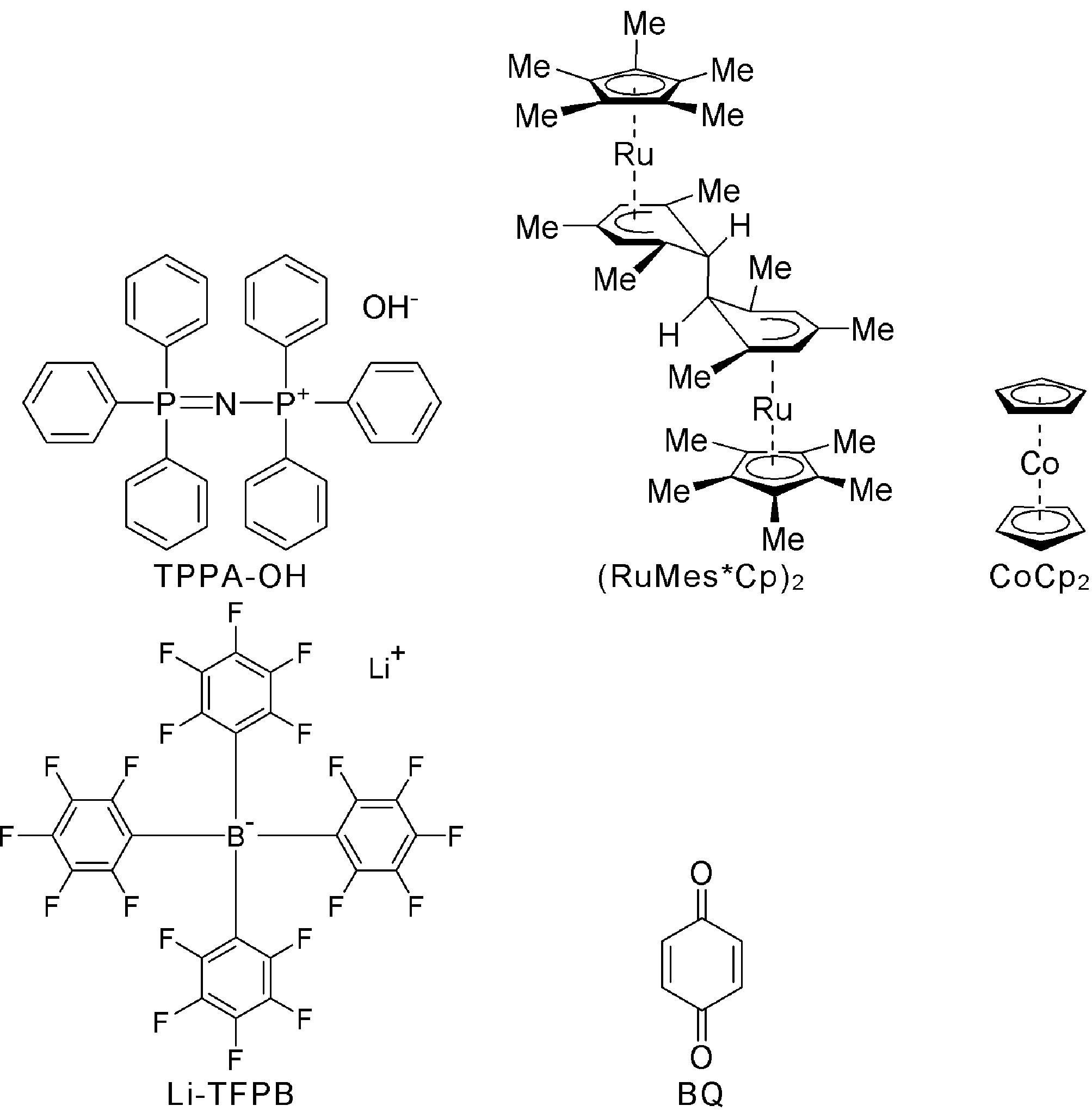
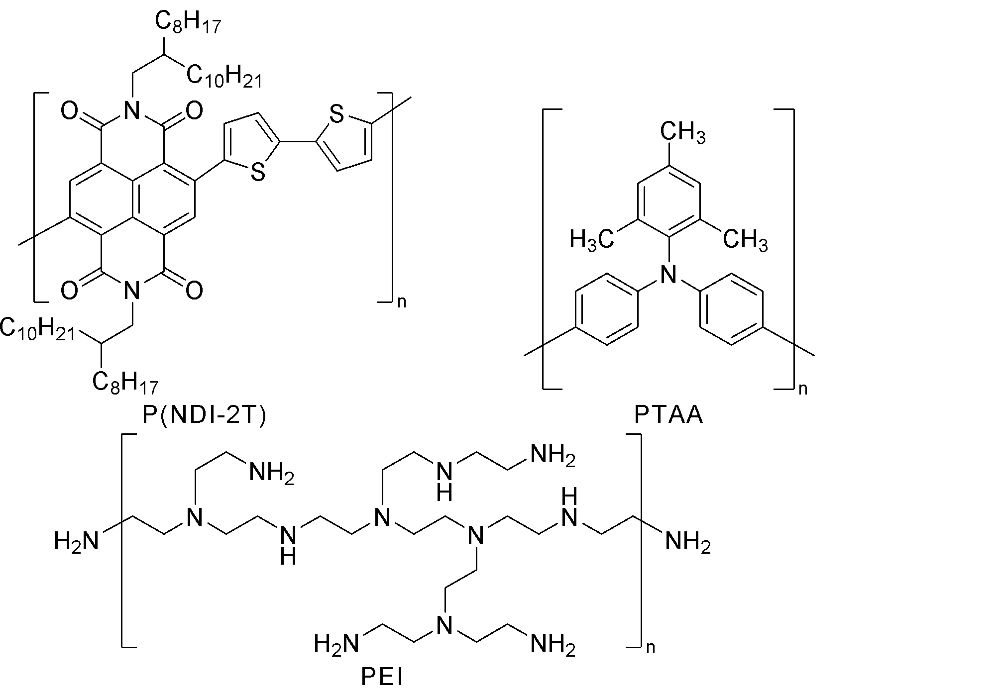
〔実施例1〕
以下の手順により、表面修飾Au電極/P(NDI-2T)/Au電極の層構造を有する縦型ダイオードを作製した。得られた縦型ダイオードの電流-電圧特性を図9に示す。
以下の手順により、表面修飾Au電極/P(NDI-2T)/Au電極の層構造を有する縦型ダイオードを作製した。得られた縦型ダイオードの電流-電圧特性を図9に示す。
(1)ガラス基板上に抵抗加熱蒸着によりAuを製膜し、Au電極を得た。
(2)TPPA-OH(1mM)、フルクトース(1M)、及びリボフラビン(50mM)を溶解した水溶液にAu電極を浸漬した。
(3)Au電極を純水で洗浄することで、表面修飾Au電極を得た。
(4)N2200(P(NDI-2T))を1wt%の濃度で含む溶液を、2,000rpm、60秒の条件で表面修飾Au電極上にスピンコートした。
(5)塗膜を80℃で20分ベークすることで、厚さ約70nmの有機半導体層を形成した。
(6)有機半導体層上にAuトップ電極(30nm)を蒸着することで、縦型ダイオードを得た。
(2)TPPA-OH(1mM)、フルクトース(1M)、及びリボフラビン(50mM)を溶解した水溶液にAu電極を浸漬した。
(3)Au電極を純水で洗浄することで、表面修飾Au電極を得た。
(4)N2200(P(NDI-2T))を1wt%の濃度で含む溶液を、2,000rpm、60秒の条件で表面修飾Au電極上にスピンコートした。
(5)塗膜を80℃で20分ベークすることで、厚さ約70nmの有機半導体層を形成した。
(6)有機半導体層上にAuトップ電極(30nm)を蒸着することで、縦型ダイオードを得た。
〔実施例2〕
以下の手順により表面が修飾されたCu電極を作製した。
以下の手順により表面が修飾されたCu電極を作製した。
(1)ガラス基板上に真空抵抗加熱蒸着によりCuを製膜し、Cu電極を得た。
(2)BQ(20mM)、Li-TFPB(5mM)、及びH2SO4(1mM)を含む水溶液にCu電極を30秒浸漬した。
(3)Cu電極を純水で洗浄し、窒素ブローにより乾燥することで、表面修飾Cu電極を得た。
(2)BQ(20mM)、Li-TFPB(5mM)、及びH2SO4(1mM)を含む水溶液にCu電極を30秒浸漬した。
(3)Cu電極を純水で洗浄し、窒素ブローにより乾燥することで、表面修飾Cu電極を得た。
表面修飾Cu電極について、21.2eVのヘリウム光源を用いた紫外光電子分光(UPS)測定を行った。表面修飾Cu電極のUPS測定結果を図10(A)に示す。また、高binding energy領域の拡大図を図10(B)示す。立ち上がり位置と光源のエネルギー(21.2eV)より、表面修飾Cu電極では、5.12eVの仕事関数が評価された。
〔比較例1〕
実施例2の操作(1)により、未修飾のCu電極を得た。
未修飾Cu電極について、21.2eVのヘリウム光源を用いた紫外光電子分光(UPS)測定を行った。未修飾Cu電極のUPS測定結果を図11(A)に示す。また、高binding energy領域の拡大図を図11(B)示す。立ち上がり位置と光源のエネルギー(21.2eV)より、未修飾Cu電極は4.66eV、未修飾Cu電極では、4.66eVの仕事関数が評価された。
実施例2の操作(1)により、未修飾のCu電極を得た。
未修飾Cu電極について、21.2eVのヘリウム光源を用いた紫外光電子分光(UPS)測定を行った。未修飾Cu電極のUPS測定結果を図11(A)に示す。また、高binding energy領域の拡大図を図11(B)示す。立ち上がり位置と光源のエネルギー(21.2eV)より、未修飾Cu電極は4.66eV、未修飾Cu電極では、4.66eVの仕事関数が評価された。
〔実施例3〕
第1電極として、実施例2と同じ条件で表面を修飾したAu電極を用い、以下の手順により、表面修飾Au電極/PTAA/Au電極の層構造を有する縦型ダイオードを作製した。得られた縦型ダイオードの電流-電圧特性を図12に示す。
第1電極として、実施例2と同じ条件で表面を修飾したAu電極を用い、以下の手順により、表面修飾Au電極/PTAA/Au電極の層構造を有する縦型ダイオードを作製した。得られた縦型ダイオードの電流-電圧特性を図12に示す。
(1)PTAAをo-ジクロロベンゼンに溶解し、2wt%PTAA溶液を調製した。この溶液を2,000rpmで60秒の条件で表面修飾Au電極上にスピンコートした。
(2)塗膜を80℃のホットプレートで20分間乾燥することで、有機半導体層を形成した。
(3)有機半導体層上に真空抵抗加熱蒸着によりAuを製膜することで、縦型ダイオードを得た。
(2)塗膜を80℃のホットプレートで20分間乾燥することで、有機半導体層を形成した。
(3)有機半導体層上に真空抵抗加熱蒸着によりAuを製膜することで、縦型ダイオードを得た。
〔実施例4〕
第1電極として、実施例2で作製した表面修飾Cu電極を用いたこと以外は、実施例3と同様にして、表面修飾Cu電極/PTAA/Au電極の層構造を有する縦型ダイオードを作製した。得られた縦型ダイオードの電流-電圧特性を図13に示す。
第1電極として、実施例2で作製した表面修飾Cu電極を用いたこと以外は、実施例3と同様にして、表面修飾Cu電極/PTAA/Au電極の層構造を有する縦型ダイオードを作製した。得られた縦型ダイオードの電流-電圧特性を図13に示す。
〔実施例5〕
(3)において、真空抵抗加熱蒸着によりCuを製膜したこと以外は、実施例4と同様にして、表面修飾Cu電極/PTAA/Cu電極の層構造を有する縦型ダイオードを作製した。得られた縦型ダイオードの電流-電圧特性を図14に示す。
(3)において、真空抵抗加熱蒸着によりCuを製膜したこと以外は、実施例4と同様にして、表面修飾Cu電極/PTAA/Cu電極の層構造を有する縦型ダイオードを作製した。得られた縦型ダイオードの電流-電圧特性を図14に示す。
〔実施例6〕
以下の手順により、表面修飾Au二層電極/P(NDI-2T)/Au電極の層構造を有する縦型ダイオードを作製した。得られた縦型ダイオードの電流-電圧特性を図15に示す。
以下の手順により、表面修飾Au二層電極/P(NDI-2T)/Au電極の層構造を有する縦型ダイオードを作製した。得られた縦型ダイオードの電流-電圧特性を図15に示す。
(1)ガラス基板に真空抵抗加熱蒸着によりCr2nmとAu20nmとを順に積層し、Au二層電極を得た。
(2)Au二層電極が形成されたガラス基板を15分間のUV/O3処理に供した。
(3)UV/O3処理後のガラス基板を、超音波洗浄機を用いてアセトン中及びイソプロパノール中において10分ずつ洗浄し、その後100℃のホットプレート上で10分間乾燥した。
(4)(RuMes*Cp)2の2mM酢酸ブチル溶液をAu二層電極上に滴下した後、10秒静置した。
(5)スピンコーターを用いてガラス基板を2,000rpmで20秒回転した。
(6)塗膜を80℃のホットプレート上で5分間乾燥した。
(7)酢酸ブチル溶媒をAu二層電極上に滴下し、スピンコーターを用いてガラス基板を2,000rpmで20秒回転することで、Au二層電極の表面を洗浄した。
(8)80℃のホットプレート上で5分間乾燥することで、表面修飾電極を得た。
(9)P(NDI-2T)をo-ジクロロベンゼン溶解し、に1wt%P(NDI-2T)溶液を得た。得られた溶液を2,000rpm、60秒の条件で表面修飾電極上にスピンコートした。
(10)塗膜を80℃のホットプレート上で20分間乾燥することで、厚さ約70nmの有機半導体層を形成した。
(11)有機半導体層上に真空抵抗加熱蒸着によりAuを30nm製膜することで、縦型ダイオードを得た。
(2)Au二層電極が形成されたガラス基板を15分間のUV/O3処理に供した。
(3)UV/O3処理後のガラス基板を、超音波洗浄機を用いてアセトン中及びイソプロパノール中において10分ずつ洗浄し、その後100℃のホットプレート上で10分間乾燥した。
(4)(RuMes*Cp)2の2mM酢酸ブチル溶液をAu二層電極上に滴下した後、10秒静置した。
(5)スピンコーターを用いてガラス基板を2,000rpmで20秒回転した。
(6)塗膜を80℃のホットプレート上で5分間乾燥した。
(7)酢酸ブチル溶媒をAu二層電極上に滴下し、スピンコーターを用いてガラス基板を2,000rpmで20秒回転することで、Au二層電極の表面を洗浄した。
(8)80℃のホットプレート上で5分間乾燥することで、表面修飾電極を得た。
(9)P(NDI-2T)をo-ジクロロベンゼン溶解し、に1wt%P(NDI-2T)溶液を得た。得られた溶液を2,000rpm、60秒の条件で表面修飾電極上にスピンコートした。
(10)塗膜を80℃のホットプレート上で20分間乾燥することで、厚さ約70nmの有機半導体層を形成した。
(11)有機半導体層上に真空抵抗加熱蒸着によりAuを30nm製膜することで、縦型ダイオードを得た。
〔交流電力から直流電力への変換効率の評価〕
縦型ダイオードに導入された交流電力を横軸にとり、交流電力から直流電力への変換効率をプロットしたグラフを図8に示す。図8中、抵抗値は可変抵抗の設定値である。図8から、実施例13で得た縦型ダイオードは、1GHzの交流電力を9%程度の効率で変換していることがわかる。これは、溶液プロセスされたダイオードの報告値より1桁以上高い効率である。
縦型ダイオードに導入された交流電力を横軸にとり、交流電力から直流電力への変換効率をプロットしたグラフを図8に示す。図8中、抵抗値は可変抵抗の設定値である。図8から、実施例13で得た縦型ダイオードは、1GHzの交流電力を9%程度の効率で変換していることがわかる。これは、溶液プロセスされたダイオードの報告値より1桁以上高い効率である。
〔実施例7〕
(5)において(RuMes*Cp)2をCoCp2に変更した以外は、実施例6と同様にして、表面修飾Au二層電極/P(NDI-2T)/Au電極の層構造を有する縦型ダイオードを作製した。得られた縦型ダイオードの電流-電圧特性を図16に示す。
(5)において(RuMes*Cp)2をCoCp2に変更した以外は、実施例6と同様にして、表面修飾Au二層電極/P(NDI-2T)/Au電極の層構造を有する縦型ダイオードを作製した。得られた縦型ダイオードの電流-電圧特性を図16に示す。
〔比較例2〕
(4)~(8)を行わなかった以外は、実施例6と同様にして、未修飾Au二層電極/P(NDI-2T)/Au電極の層構造を有する縦型ダイオードを作製した。得られた縦型ダイオードの電流-電圧特性を図17に示す。
(4)~(8)を行わなかった以外は、実施例6と同様にして、未修飾Au二層電極/P(NDI-2T)/Au電極の層構造を有する縦型ダイオードを作製した。得られた縦型ダイオードの電流-電圧特性を図17に示す。
〔低分子疎水性イオン被覆率の評価〕
比較例2で得た未修飾Au二層電極及び実施例6で得た表面修飾Au二層電極のXPS元素分析を行った。結果を図18に示す。
未修飾Au二層電極でも、炭素のごみによるC1sピークが少し観測された。
表面修飾Au二層電極では、C1s及びRu3dの強度が強くなった。
Ru3d及びAu3dの強度から、Au二層電極表面にどの程度の密度でRu錯体分子カチオンが堆積しているかを求めた。Ru錯体分子カチオン層の厚みは、単分子層以下(1nm以下)であり、Au二層電極の30面積%程度を被覆していることがわかった。
比較例2で得た未修飾Au二層電極及び実施例6で得た表面修飾Au二層電極のXPS元素分析を行った。結果を図18に示す。
未修飾Au二層電極でも、炭素のごみによるC1sピークが少し観測された。
表面修飾Au二層電極では、C1s及びRu3dの強度が強くなった。
Ru3d及びAu3dの強度から、Au二層電極表面にどの程度の密度でRu錯体分子カチオンが堆積しているかを求めた。Ru錯体分子カチオン層の厚みは、単分子層以下(1nm以下)であり、Au二層電極の30面積%程度を被覆していることがわかった。
〔実施例8〕
以下の手順により、(RuMes*Cp)2由来の低分子疎水性閉殻カチオンで表面が修飾されたITO電極を作製した。得られた表面修飾ITO電極の光電子収量分光法(PYS)測定を行った。結果を図19及び表1に示す。
以下の手順により、(RuMes*Cp)2由来の低分子疎水性閉殻カチオンで表面が修飾されたITO電極を作製した。得られた表面修飾ITO電極の光電子収量分光法(PYS)測定を行った。結果を図19及び表1に示す。
(1)5分間のUV/O3処理により、ITO電極表面を洗浄した。
(2)(RuMes*Cp)2の2mM酢酸ブチル溶液をUV/O3処理したITO電極に滴下し、10秒静置した後に3,000rpm、60秒の条件でスピンコートした。
(3)塗膜を80℃のホットプレート上で5分間乾燥した。
(4)酢酸ブチルをITO電極に滴下し、3,000rpmで60秒を回転することでITO電極表面を洗浄した。
(5)洗浄後のITO電極を80℃のホットプレート上で5分間乾燥することで、表面修飾ITO電極を得た。
(2)(RuMes*Cp)2の2mM酢酸ブチル溶液をUV/O3処理したITO電極に滴下し、10秒静置した後に3,000rpm、60秒の条件でスピンコートした。
(3)塗膜を80℃のホットプレート上で5分間乾燥した。
(4)酢酸ブチルをITO電極に滴下し、3,000rpmで60秒を回転することでITO電極表面を洗浄した。
(5)洗浄後のITO電極を80℃のホットプレート上で5分間乾燥することで、表面修飾ITO電極を得た。
〔比較例3〕
実施例8の操作(1)により、未修飾ITO電極を作製した。
実施例8の操作(1)により、未修飾ITO電極を作製した。
〔比較例4〕
以下の手順によりPEIで表面が修飾されたITO電極を作製した。得られた表面修飾ITO電極の光電子収量分光法(PYS)測定を行った。結果を図21及び表1に示す。
以下の手順によりPEIで表面が修飾されたITO電極を作製した。得られた表面修飾ITO電極の光電子収量分光法(PYS)測定を行った。結果を図21及び表1に示す。
(1)5分間のUV/O3処理により、ITO電極表面を洗浄した。
(2)PEIを純水に溶解して調製された0.2wt%PEI水溶液をITO電極に滴下し、10秒静置した後に3,000rpm、60秒の条件でスピンコートした。
(3)塗膜を90℃のホットプレート上で30分間乾燥した。
(4)酢酸ブチルをITO電極に滴下し、3,000rpmで60秒を回転することでITO電極表面を洗浄した。
(5)洗浄後のITO電極を80℃のホットプレート上で5分間乾燥することで、表面修飾ITO電極を得た。
(2)PEIを純水に溶解して調製された0.2wt%PEI水溶液をITO電極に滴下し、10秒静置した後に3,000rpm、60秒の条件でスピンコートした。
(3)塗膜を90℃のホットプレート上で30分間乾燥した。
(4)酢酸ブチルをITO電極に滴下し、3,000rpmで60秒を回転することでITO電極表面を洗浄した。
(5)洗浄後のITO電極を80℃のホットプレート上で5分間乾燥することで、表面修飾ITO電極を得た。
〔仕事関数の評価〕
実施例8で得た表面修飾ITO電極、比較例3で得た未修飾ITO電極、及び比較例4で得た表面修飾ITO電極の光電子収量分光法(PYS)測定を行った。実施例8、比較例3、比較例4の測定結果を、それぞれ、図19~21に示す。また、求めた仕事関数を表1に示す。
実施例8で得た表面修飾ITO電極、比較例3で得た未修飾ITO電極、及び比較例4で得た表面修飾ITO電極の光電子収量分光法(PYS)測定を行った。実施例8、比較例3、比較例4の測定結果を、それぞれ、図19~21に示す。また、求めた仕事関数を表1に示す。

〔表面組成分析〕
実施例8で得た表面修飾ITO電極及び比較例3で得た未修飾ITO電極のXPS元素分析を行った。結果を図22及び表2に示す。図22より、実施例8で得た表面修飾ITO電極では、ITO電極の表面に(RuCp*Mes)2由来の低分子疎水性閉殻カチオンの層が形成されていることがわかる。
実施例8で得た表面修飾ITO電極及び比較例3で得た未修飾ITO電極のXPS元素分析を行った。結果を図22及び表2に示す。図22より、実施例8で得た表面修飾ITO電極では、ITO電極の表面に(RuCp*Mes)2由来の低分子疎水性閉殻カチオンの層が形成されていることがわかる。
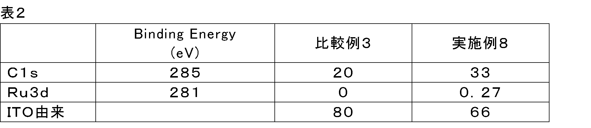
〔低分子疎水性閉殻カチオンの層の層厚の評価〕
ITO電極表面にカチオンが単分子層で堆積した場合の元素構成のシミュレーションを行った。シミュレーション結果を表3に示す。
ITO電極表面にカチオンが単分子層で堆積した場合の元素構成のシミュレーションを行った。シミュレーション結果を表3に示す。

実施例8で得た表面修飾ITO電極のXPS測定により求めたRuの構成比は、単分子層堆積モデルの1/10であったことから、実施例8では、(RuCp*Mes)2由来の低分子疎水性閉殻カチオンの層の層厚が、単分子層以下(1nm以下)であることがわかる。
また、実施例8では、酸化還元反応により電子注入と低分子疎水性閉殻カチオンの堆積が生じる、電場及び真空準位シフトが生じて表面修飾ITO電極の仕事関数が減少したと考えられえる。
また、実施例8では、酸化還元反応により電子注入と低分子疎水性閉殻カチオンの堆積が生じる、電場及び真空準位シフトが生じて表面修飾ITO電極の仕事関数が減少したと考えられえる。
〔実施例9〕
以下の手順により、表面修飾ITO電極/P(NDI-2T)/Au電極の層構造を有する縦型ダイオードを作製した。
以下の手順により、表面修飾ITO電極/P(NDI-2T)/Au電極の層構造を有する縦型ダイオードを作製した。
(1)5分間のUV/O3処理により、ITO電極表面を洗浄した。
(2)(RuMes*Cp)2の2mM酢酸ブチル溶液をUV/O3処理したITOに滴下し、10秒静置した後に3,000rpm、60秒の条件でスピンコートした。
(3)塗膜を80℃のホットプレート上で5分間乾燥した。
(4)酢酸ブチルをITO電極に滴下し、3,000rpmで60秒を回転することでITO電極表面を洗浄した。
(5)洗浄後のITO電極を80℃のホットプレート上で5分間乾燥することで、表面修飾ITO電極を得た。
(6)表面修飾ITO電極の上にP(NDI-2T)をo-ジクロロベンゼンに溶解させて調製した1wt%P(NDI-2T)溶液を2,000rpm、60秒の条件でスピンコートした。
(7)塗膜を80℃のホットプレート上で20分間乾燥することで、厚さ約70nmの有機半導体層を形成した。
(8)有機半導体層上に、真空抵抗加熱蒸着機を用いて高真空状態でAuを40nm蒸着することで、縦型ダイオードを得た。
(2)(RuMes*Cp)2の2mM酢酸ブチル溶液をUV/O3処理したITOに滴下し、10秒静置した後に3,000rpm、60秒の条件でスピンコートした。
(3)塗膜を80℃のホットプレート上で5分間乾燥した。
(4)酢酸ブチルをITO電極に滴下し、3,000rpmで60秒を回転することでITO電極表面を洗浄した。
(5)洗浄後のITO電極を80℃のホットプレート上で5分間乾燥することで、表面修飾ITO電極を得た。
(6)表面修飾ITO電極の上にP(NDI-2T)をo-ジクロロベンゼンに溶解させて調製した1wt%P(NDI-2T)溶液を2,000rpm、60秒の条件でスピンコートした。
(7)塗膜を80℃のホットプレート上で20分間乾燥することで、厚さ約70nmの有機半導体層を形成した。
(8)有機半導体層上に、真空抵抗加熱蒸着機を用いて高真空状態でAuを40nm蒸着することで、縦型ダイオードを得た。
〔比較例5〕
以下の手順により、縦型ダイオードを作製した。
以下の手順により、縦型ダイオードを作製した。
(1)5分間のUV/O3処理により、ITO電極表面を洗浄し、未修飾ITO電極を得た。
(2)ITO電極の上にP(NDI-2T)をo-ジクロロベンゼンに溶解させて調製した1wt%P(NDI-2T)溶液を2,000rpm、60秒の条件でスピンコートした。
(3)塗膜を80℃のホットプレート上で20分間乾燥することで、有機半導体層を形成した。
(4)有機半導体層上に、真空抵抗加熱蒸着機を用いて高真空状態でAuを40nm蒸着することで、縦型ダイオードを得た。
(2)ITO電極の上にP(NDI-2T)をo-ジクロロベンゼンに溶解させて調製した1wt%P(NDI-2T)溶液を2,000rpm、60秒の条件でスピンコートした。
(3)塗膜を80℃のホットプレート上で20分間乾燥することで、有機半導体層を形成した。
(4)有機半導体層上に、真空抵抗加熱蒸着機を用いて高真空状態でAuを40nm蒸着することで、縦型ダイオードを得た。
〔低分子疎水性イオン被覆率の評価〕
実施例9で得た表面修飾ITO電極及び比較例5で得た未修飾ITO電極のXPS元素分析を行った。実施例9及び比較例5の測定結果を、それぞれ、図23及び図24に示す。
実施例9で得た表面修飾ITO電極及び比較例5で得た未修飾ITO電極のXPS元素分析を行った。実施例9及び比較例5の測定結果を、それぞれ、図23及び図24に示す。
表面修飾により、C1sの増加及びRu3dが見られるようになり、(RuMes*Cp)2由来のカチオンが堆積していることが示された(図23参照)。
また、Ru3d強度とITOに由来する強度の比較から、実施例8で得た表面修飾ITO電極における低分子疎水性イオン被覆率は、30面積%程度であることが示された。
また、Ru3d強度とITOに由来する強度の比較から、実施例8で得た表面修飾ITO電極における低分子疎水性イオン被覆率は、30面積%程度であることが示された。
〔実施例10〕
以下の手順により、表面修飾ITO電極/P(NDI-2T)/Au電極の層構造を有する縦型ダイオードを作製した。
以下の手順により、表面修飾ITO電極/P(NDI-2T)/Au電極の層構造を有する縦型ダイオードを作製した。
(1)5分間のUV/O3処理により、ITO電極表面を洗浄した。
(2)(RuMes*Cp)2の2mM酢酸ブチル溶液をUV/O3処理したITO電極に滴下し、10秒静置した後に3,000rpm、60秒の条件でスピンコートした。
(3)塗膜を80℃のホットプレート上で5分間乾燥した。
(4)酢酸ブチルをITO電極に滴下し、3,000rpmで60秒を回転することでITO電極表面を洗浄した。
(5)洗浄後のITO電極を80℃のホットプレート上で5分間乾燥することで、表面修飾ITO電極を得た。
(6)表面修飾ITO基板の上にP(NDI-2T)をo-ジクロロベンゼンに溶解させて調製した1wt%P(NDI-2T)溶液を2,000rpm、60秒の条件でスピンコートした。
(7)塗膜を80℃のホットプレート上で20分間乾燥することで、厚さ約70nmの有機半導体層を形成した。
(8)有機半導体層上に、真空抵抗加熱蒸着機を用いて高真空状態でAuを40nm蒸着することで、縦型ダイオードを得た。
(2)(RuMes*Cp)2の2mM酢酸ブチル溶液をUV/O3処理したITO電極に滴下し、10秒静置した後に3,000rpm、60秒の条件でスピンコートした。
(3)塗膜を80℃のホットプレート上で5分間乾燥した。
(4)酢酸ブチルをITO電極に滴下し、3,000rpmで60秒を回転することでITO電極表面を洗浄した。
(5)洗浄後のITO電極を80℃のホットプレート上で5分間乾燥することで、表面修飾ITO電極を得た。
(6)表面修飾ITO基板の上にP(NDI-2T)をo-ジクロロベンゼンに溶解させて調製した1wt%P(NDI-2T)溶液を2,000rpm、60秒の条件でスピンコートした。
(7)塗膜を80℃のホットプレート上で20分間乾燥することで、厚さ約70nmの有機半導体層を形成した。
(8)有機半導体層上に、真空抵抗加熱蒸着機を用いて高真空状態でAuを40nm蒸着することで、縦型ダイオードを得た。
〔比較例6〕
(2)~(5)を行わなかった以外は、実施例10と同様にして、未修飾ITO電極/P(NDI-2T)/Au電極の層構造を有する縦型ダイオードを作製した。
(2)~(5)を行わなかった以外は、実施例10と同様にして、未修飾ITO電極/P(NDI-2T)/Au電極の層構造を有する縦型ダイオードを作製した。
〔整流比の評価〕
実施例10で得た縦型ダイオード及び比較例6で得た縦型ダイオードの電流-電圧特性を、それぞれ、図25及び図26に示す。また、これらの縦型ダイオードの順方向電流、逆方向電流、及び整流比を表4に示す。表4から、表面修飾によりITO電極から有機半導体層への電子注入特性が向上したことがわかる。
実施例10で得た縦型ダイオード及び比較例6で得た縦型ダイオードの電流-電圧特性を、それぞれ、図25及び図26に示す。また、これらの縦型ダイオードの順方向電流、逆方向電流、及び整流比を表4に示す。表4から、表面修飾によりITO電極から有機半導体層への電子注入特性が向上したことがわかる。

〔実施例11〕
以下の手順により、表面修飾Au電極/PTAA(ドープ層)/Au電極の層構造を有する縦型ダイオードを作製した。
以下の手順により、表面修飾Au電極/PTAA(ドープ層)/Au電極の層構造を有する縦型ダイオードを作製した。
(1)Au電極をUV/O3処理した。
(2)Au電極を、ヒドロキノンHQ(1mM)及び1,3-ジメチルイミダゾリウムヒドロキシド(0.1mM)を含む水溶液に30秒浸漬し、窒素ブローにより乾燥することで、表面修飾Au電極を得た。
(3)PTAAをo-ジクロロベンゼンに溶解し、2wt%PTAA溶液を調製した。この溶液を2,000rpm、60秒の条件で表面修飾Au電極上にスピンコートした。
(4)塗膜を80℃のホットプレートで20分間乾燥することで、有機半導体層を形成した。
(5)有機半導体層の表面近傍にホールをドーピングするため、Au電極上に形成された有機半導体層を、硫酸(1mM)、ベンゾキノン(10mM)、及びリチウムテトラキス(ペンタフルオロフェニル)ボレート(10mM)を含む水溶液に30秒浸漬し、その後純水ですすいで洗浄した。
(6)有機半導体層の上に、真空抵抗加熱蒸着によりAu電極を形成することで、縦型ダイオードを得た。
(2)Au電極を、ヒドロキノンHQ(1mM)及び1,3-ジメチルイミダゾリウムヒドロキシド(0.1mM)を含む水溶液に30秒浸漬し、窒素ブローにより乾燥することで、表面修飾Au電極を得た。
(3)PTAAをo-ジクロロベンゼンに溶解し、2wt%PTAA溶液を調製した。この溶液を2,000rpm、60秒の条件で表面修飾Au電極上にスピンコートした。
(4)塗膜を80℃のホットプレートで20分間乾燥することで、有機半導体層を形成した。
(5)有機半導体層の表面近傍にホールをドーピングするため、Au電極上に形成された有機半導体層を、硫酸(1mM)、ベンゾキノン(10mM)、及びリチウムテトラキス(ペンタフルオロフェニル)ボレート(10mM)を含む水溶液に30秒浸漬し、その後純水ですすいで洗浄した。
(6)有機半導体層の上に、真空抵抗加熱蒸着によりAu電極を形成することで、縦型ダイオードを得た。
〔実施例12〕
(5)を行わなかった以外は、実施例11と同様にして、表面修飾Au電極/PTAA/Au電極の層構造を有する縦型ダイオードを作製した。
(5)を行わなかった以外は、実施例11と同様にして、表面修飾Au電極/PTAA/Au電極の層構造を有する縦型ダイオードを作製した。
〔整流比の評価〕
実施例11で得た縦型ダイオード及び実施例12で得た縦型ダイオードの電流-電圧特性を、それぞれ、図27及び図28に示す。
図27及び図28より、Au電極近傍にドープ層を形成した実施例11では、逆方向電流が抑制され、実施例12よりも整流比が高くなっていることがわかる。また、実施例11及び実施例12で得られた縦型ダイオードは、電圧が3Vのときの電流密度が100Acm-2程度であり、低電圧でも高い電流密度を示すことがわかる。
実施例11で得た縦型ダイオード及び実施例12で得た縦型ダイオードの電流-電圧特性を、それぞれ、図27及び図28に示す。
図27及び図28より、Au電極近傍にドープ層を形成した実施例11では、逆方向電流が抑制され、実施例12よりも整流比が高くなっていることがわかる。また、実施例11及び実施例12で得られた縦型ダイオードは、電圧が3Vのときの電流密度が100Acm-2程度であり、低電圧でも高い電流密度を示すことがわかる。
〔実施例13〕
(9)において、P(NDI-2T)溶液におけるP(NDI-2T)濃度を0.5wt%に変更した以外は、実施例6と同様にして、表面修飾Au二層電極/P(NDI-2T)/Au電極の層構造を有する縦型ダイオードを作製した。この縦型ダイオードのP(NDI-2T)層の厚さは、25nmであった。得られた縦型ダイオードの電流-電圧特性を図29に示す。
(9)において、P(NDI-2T)溶液におけるP(NDI-2T)濃度を0.5wt%に変更した以外は、実施例6と同様にして、表面修飾Au二層電極/P(NDI-2T)/Au電極の層構造を有する縦型ダイオードを作製した。この縦型ダイオードのP(NDI-2T)層の厚さは、25nmであった。得られた縦型ダイオードの電流-電圧特性を図29に示す。
実施例13で得た縦型ダイオードは、有機半導体層の厚さが25nmと非常に薄いものであったが、図29から、整流特性に優れ、低電圧における電流密度も高いことがわかる。
〔1GHzにおける10%整流の評価〕
図6に示す回路を用いて1GHzにおける10%整流の評価を行った。
Signal Generator(波形発生器)により生じた1GHzの交流シグナルをアンプにより増幅し、この交流電力をパワーメータによりP1として評価した。
なお、電力のうちダイオードに導入されずに反射される成分はパワーメータを用いてP2として計測した。
図6に示す回路を用いて1GHzにおける10%整流の評価を行った。
Signal Generator(波形発生器)により生じた1GHzの交流シグナルをアンプにより増幅し、この交流電力をパワーメータによりP1として評価した。
なお、電力のうちダイオードに導入されずに反射される成分はパワーメータを用いてP2として計測した。
縦型ダイオードに交流電力が導入されると整流され、直流電力へと変換される。この直流電力はバイアスティーによりつながれた可変抵抗へ導入される。この可変抵抗の抵抗値とその両端に生じる電圧V3から、縦型ダイオードにより変換された直流電力の大きさを評価した。電圧V3は、電圧計により計測した。結果を図7に示す。
〔交流電力から直流電力への変換効率の評価〕
縦型ダイオードに70mW又は42mWの交流電力導入した際の可変抵抗の抵抗値を横軸にとり、交流電力から直流電力への変換効率を横軸にとってプロットしたグラフを図30に示す。図30から、実施例13で得た縦型ダイオードは、1GHzの交流電力を8%程度の効率で変換していることがわかる。これは、溶液プロセスされたダイオードの報告値より1桁以上高い効率である。
縦型ダイオードに70mW又は42mWの交流電力導入した際の可変抵抗の抵抗値を横軸にとり、交流電力から直流電力への変換効率を横軸にとってプロットしたグラフを図30に示す。図30から、実施例13で得た縦型ダイオードは、1GHzの交流電力を8%程度の効率で変換していることがわかる。これは、溶液プロセスされたダイオードの報告値より1桁以上高い効率である。
〔実施例14〕
(1)ガラス基板上に抵抗加熱蒸着によりAuを製膜し、フォトリソグラフィを用いたパターニングを用いることでAu電極を得た。
(2)TPPA-OH(0.25mM)、フルクトース(1M)、及びリボフラビン(10mM)を溶解した水溶液にAu電極を浸漬した。
(3)Au電極を純水で洗浄することで、表面修飾Au電極を得た。
(4)N2200(P(NDI-2T))を0.8wt%の濃度で含む溶液を、2,000rpm、60秒の条件で表面修飾Au電極上にスピンコートした。
(5)塗膜を80℃で20分ベークすることで、厚さ約40nmの有機半導体層を形成した。
(6)有機半導体層上にAuトップ電極(30nm)を蒸着し、フォトリソグラフィを用いたAuトップ電極のパターニングを実施することで、縦型ダイオードを得た。
(1)ガラス基板上に抵抗加熱蒸着によりAuを製膜し、フォトリソグラフィを用いたパターニングを用いることでAu電極を得た。
(2)TPPA-OH(0.25mM)、フルクトース(1M)、及びリボフラビン(10mM)を溶解した水溶液にAu電極を浸漬した。
(3)Au電極を純水で洗浄することで、表面修飾Au電極を得た。
(4)N2200(P(NDI-2T))を0.8wt%の濃度で含む溶液を、2,000rpm、60秒の条件で表面修飾Au電極上にスピンコートした。
(5)塗膜を80℃で20分ベークすることで、厚さ約40nmの有機半導体層を形成した。
(6)有機半導体層上にAuトップ電極(30nm)を蒸着し、フォトリソグラフィを用いたAuトップ電極のパターニングを実施することで、縦型ダイオードを得た。
〔整流比の評価〕
実施例14で得た縦型ダイオードの電流-電圧特性を図31に示す。
図31より、大気雰囲気下で電極の表面を修飾した場合であっても、整流ダイオードに適した高い整流比及び高い電流値を実現できることがわかる。
実施例14で得た縦型ダイオードの電流-電圧特性を図31に示す。
図31より、大気雰囲気下で電極の表面を修飾した場合であっても、整流ダイオードに適した高い整流比及び高い電流値を実現できることがわかる。
Claims (39)
- 第1電極、有機半導体層、及び第2電極がこの順に隣接して積層された縦型ダイオードであって、
前記第1電極の表面であって前記有機半導体層と隣接する面に低分子疎水性イオンが付着している、縦型ダイオード。 - 前記低分子疎水性イオンが、低分子疎水性閉殻イオンである、請求項1に記載の縦型ダイオード。
- 前記低分子疎水性イオンが、低分子疎水性カチオンであり、
前記低分子疎水性カチオンが、式(1A)~(1F)で表されるカチオンからなる群より選択される1種以上である、請求項1に記載の縦型ダイオード。
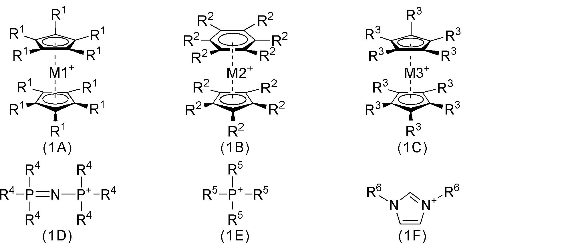
(式中、M1は、ロジウム又はイリジウムであり;M2は、ルテニウムであり;M3は、コバルトであり;R1~R6は、それぞれ独立して、水素原子、置換基を有していてもよいアルキル基、又は置換基を有していてもよいアリール基である。) - 前記低分子疎水性イオンが、低分子疎水性アニオンであり、
前記低分子疎水性アニオンが、式(3F)~(3G)で表されるアニオンからなる群より選択される1種以上である、請求項1に記載の縦型ダイオード。
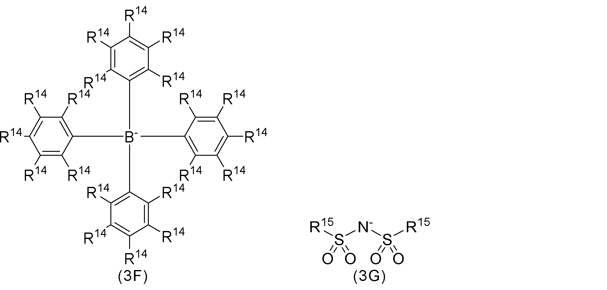
(式中、R14は、それぞれ独立して、水素原子、ハロゲン原子、又は置換基を有していてもよいフッ化アルキル基であり;R15は、それぞれ独立して、パーフルオロアルキル基であり、2つのR15は、互いに連結して環を形成していてもよい。) - 前記低分子疎水性イオンが、前記第1電極の表面であって前記有機半導体層と隣接する面の10面積%以上50面積%以下に付着している、請求項1に記載の縦型ダイオード。
- 前記低分子疎水性イオンが、前記第1電極の表面であって前記有機半導体層と隣接する面の上でイオン層を形成しており、
前記イオン層の厚さが、2nm以下又は3分子層以下の厚さである、請求項1に記載の縦型ダイオード。 - 前記第1電極の表面であって前記有機半導体層と隣接する面に付着している前記低分子疎水性イオンのうち、対イオンと塩を形成している低分子疎水性イオンの割合が、25mol%以下であり、
前記対イオンが、前記有機半導体層を構成する有機半導体に由来するイオン、プロトン、水酸化物イオン、及び前記第1電極に含まれる金属のイオン以外の対イオンである、請求項1に記載の縦型ダイオード。 - 前記第1電極が、銅電極である、請求項1に記載の縦型ダイオード。
- 前記低分子疎水性イオンが、低分子疎水性カチオンであり、
前記有機半導体層が、ドープ層とアンドープ層とを有し、
前記ドープ層が、前記第2電極と隣接する層であり、かつ、ホール及びドーパントアニオンを含む、請求項1に記載の縦型ダイオード。 - 前記低分子疎水性イオンが、低分子疎水性アニオンであり、
前記有機半導体層が、ドープ層とアンドープ層とを有し、
前記ドープ層が、前記第2電極と隣接する層であり、かつ、電子及びドーパントカチオンを含む、請求項1に記載の縦型ダイオード。 - 前記有機半導体層の厚さが、15nm以上50nm以下である、請求項1に記載の縦型ダイオード。
- 周波数10MHzの交流電力から直流電力への変換効率が5%超である、請求項1に記載の縦型ダイオード。
- 周波数1GHzの交流電力から直流電力への変換効率が5%超である、請求項1に記載の縦型ダイオード。
- 第1電極、有機半導体層、及び第2電極がこの順に隣接して積層された縦型ダイオードの製造方法であって、
前記第1電極の表面と表面修飾液とを接触させることで、表面修飾された第1電極を得る電極修飾工程と、
前記電極修飾工程で修飾された前記第1電極の前記表面と前記有機半導体層とが接触するよう、前記第1電極と前記有機半導体層とを積層する積層工程とを含み、
前記表面修飾液が、下記表面修飾液(S1)~(S4)のいずれかである、縦型ダイオードの製造方法。
(S1)前記第1電極を還元するとともに低分子疎水性カチオンを生じる第1還元剤を含む表面修飾液。
(S2)前記第1電極を酸化するとともに低分子疎水性アニオンを生じる第1酸化剤を含む表面修飾液。
(S3)前記第1電極を還元する第2還元剤と低分子疎水性閉殻カチオンとを含む表面修飾液。
(S4)前記第1電極を酸化する第2酸化剤と低分子疎水性閉殻アニオンとを含む表面修飾液。 - 前記表面修飾液(S1)が、前記第1還元剤から生じる前記低分子疎水性カチオンとは異なる低分子疎水性カチオンをさらに含む、請求項14に記載の縦型ダイオードの製造方法。
- 前記表面修飾液(S2)が、前記第1酸化剤から生じる前記低分子疎水性アニオンとは異なる低分子疎水性アニオンをさらに含む、請求項14に記載の縦型ダイオードの製造方法。
- 前記表面修飾液が、前記表面修飾液(S1)又は前記表面修飾液(S2)である、請求項14に記載の縦型ダイオードの製造方法。
- 前記表面修飾液が、前記表面修飾液(S3)又は前記表面修飾液(S4)である、請求項14に記載の縦型ダイオードの製造方法。
- 前記表面修飾液の溶媒が水であり、前記電極修飾工程が大気雰囲気下で行われる、請求項14に記載の縦型ダイオードの製造方法。
- 前記有機半導体層が、ドープ層とアンドープ層とを有する有機半導体層であり、かつ、前記ドープ層が前記第2電極に隣接する層であり、
第3酸化剤及び第3還元剤からなる群より選択される1種以上並びにドーパントイオンの塩を含む水溶液と、有機半導体層前駆体の表面とを接触させることで、前記ドープ層を形成するドーピング工程と、
前記有機半導体層と前記第2電極とを、前記ドープ層と前記第2電極とが接触するよう積層する積層工程と、
をさらに含む、請求項14に記載の縦型ダイオードの製造方法。 - 前記第3還元剤が、ヒドロキノン骨格を有するヒドロキノン化合物及び還元型補酵素からなる群より選択される1種以上であり、
前記第3酸化剤が、キノン骨格を有するキノン化合物である、請求項20に記載の縦型ダイオードの製造方法。 - 電極の表面を修飾し、前記電極の仕事関数を変化させるための表面修飾液であって、
前記表面修飾液が、下記表面修飾液(S1)~(S4)のいずれかである、表面修飾液。
(S1)前記電極を還元するとともに低分子疎水性カチオンを生じる第1還元剤を含む表面修飾液。
(S2)前記電極を酸化するとともに低分子疎水性アニオンを生じる第1酸化剤を含む表面修飾液。
(S3)前記電極を還元する第2還元剤と低分子疎水性閉殻カチオンとを含む表面修飾液。
(S4)前記電極を酸化する第2酸化剤と低分子疎水性閉殻アニオンとを含む表面修飾液。 - 前記表面修飾液(S1)が、前記第1還元剤から生じる前記低分子疎水性カチオンとは異なる低分子疎水性カチオンをさらに含む、請求項22に記載の表面修飾液。
- 前記表面修飾液(S2)が、前記第1酸化剤から生じる前記低分子疎水性アニオンとは異なる低分子疎水性アニオンをさらに含む、請求項22に記載の表面修飾液。
- 前記表面修飾液が、前記表面修飾液(S1)又は前記表面修飾液(S2)である、請求項22に記載の表面修飾液。
- 前記表面修飾液が、前記表面修飾液(S3)又は前記表面修飾液(S4)である、請求項22に記載の表面修飾液。
- 前記表面修飾液の溶媒が水である、請求項22に記載の表面修飾液。
- 第1電極、ドープ層とアンドープ層とを有する有機半導体層、及び第2電極がこの順に隣接して、かつ、前記ドープ層が前記第1電極又は前記第2電極に隣接して積層された縦型ダイオードであって、
前記ドープ層が、キャリア及びドーパントイオンを含み、
前記ドーパントイオンが、疎水性閉殻イオンである、縦型ダイオード。 - 前記ドープ層が、前記第2電極と隣接する層であり、
前記キャリアが、ホールであり、
前記ドーパントイオンが、疎水性閉殻アニオンであり、
前記第1電極の表面であって前記有機半導体層と隣接する面に低分子疎水性閉殻カチオンが付着している、請求項28に記載の縦型ダイオード。 - 前記ドープ層が、前記第2電極と隣接する層であり、
前記キャリアが、電子であり、
前記ドーパントイオンが疎水性閉殻カチオンであり、
前記第1電極の表面であって前記有機半導体層と隣接する面に低分子疎水性閉殻アニオンが付着している、請求項28に記載の縦型ダイオード。 - 前記ドープ層に含まれる前記ドーパントイオンのうち、対イオンと塩を形成している前記ドーパントイオンの割合が、25mol%以下であり、
前記対イオンが、前記有機半導体層を構成する有機半導体に由来するイオン、プロトン、水酸化物イオン、前記第1電極に含まれる金属のイオン、及び前記第2電極に含まれる金属のイオンである、請求項28に記載の縦型ダイオード。 - 前記ドープ層を構成する有機半導体が、前記アンドープ層を構成する有機半導体と同一の化合物である、請求項28に記載の縦型ダイオード。
- 前記有機半導体層の厚さが、15nm以上50nm以下である、請求項28に記載の縦型ダイオード。
- 第1電極、ドープ層とアンドープ層とを有する有機半導体層、及び第2電極がこの順に隣接して、かつ、前記ドープ層が前記第1電極又は前記第2電極に隣接して積層された縦型ダイオードの製造方法であって、
第4酸化剤又は第4還元剤及びドーパントイオンの塩を含む水溶液と、有機半導体層前駆体の表面とを接触させることで、前記ドープ層を形成するドーピング工程を含み、
記ドーパントイオンが、疎水性閉殻イオンである、縦型ダイオードの製造方法。 - 前記第4還元剤が、ヒドロキノン骨格を有するヒドロキノン化合物及び還元型補酵素からなる群より選択される1種以上であり、
前記第4酸化剤が、キノン骨格を有するキノン化合物である、請求項34に記載の縦型ダイオードの製造方法。 - 前記ドープ層が、前記第2電極に隣接する層であり、
前記第1電極の表面と、表面修飾液とを接触させることで、第1電極の表面を修飾する電極修飾工程をさらに含み、
前記表面修飾液が、下記表面修飾液(S1)~(S4)のいずれかである、請求項34に記載の縦型ダイオードの製造方法。
(S1)前記第1電極を還元するとともに低分子疎水性カチオンを生じる第1還元剤を含む表面修飾液。
(S2)前記第1電極を酸化するとともに低分子疎水性アニオンを生じる第1酸化剤を含む表面修飾液。
(S3)前記第1電極を還元する第2還元剤と低分子疎水性閉殻カチオンとを含む表面修飾液。
(S4)前記第1電極を酸化する第2酸化剤と低分子疎水性閉殻アニオンとを含む表面修飾液。 - 前記表面修飾液が、前記表面修飾液(S1)又は前記表面修飾液(S2)である、請求項36に記載の縦型ダイオードの製造方法。
- 前記表面修飾液が、前記表面修飾液(S3)又は前記表面修飾液(S4)である、請求項36に記載の縦型ダイオードの製造方法。
- 前記表面修飾液の溶媒が水であり、前記電極修飾工程が大気雰囲気下で行われる、請求項36に記載の縦型ダイオードの製造方法。
Priority Applications (1)
| Application Number | Priority Date | Filing Date | Title |
|---|---|---|---|
| JP2025544565A JPWO2025053187A1 (ja) | 2023-09-04 | 2024-09-04 |
Applications Claiming Priority (2)
| Application Number | Priority Date | Filing Date | Title |
|---|---|---|---|
| JP2023143258 | 2023-09-04 | ||
| JP2023-143258 | 2023-09-04 |
Publications (1)
| Publication Number | Publication Date |
|---|---|
| WO2025053187A1 true WO2025053187A1 (ja) | 2025-03-13 |
Family
ID=94924122
Family Applications (1)
| Application Number | Title | Priority Date | Filing Date |
|---|---|---|---|
| PCT/JP2024/031773 Ceased WO2025053187A1 (ja) | 2023-09-04 | 2024-09-04 | 縦型ダイオード及び縦型ダイオードの製造方法 |
Country Status (3)
| Country | Link |
|---|---|
| JP (1) | JPWO2025053187A1 (ja) |
| TW (1) | TW202531875A (ja) |
| WO (1) | WO2025053187A1 (ja) |
Citations (5)
| Publication number | Priority date | Publication date | Assignee | Title |
|---|---|---|---|---|
| JPS63237563A (ja) * | 1987-03-26 | 1988-10-04 | Mitsubishi Electric Corp | 整流素子 |
| JPH02260575A (ja) * | 1989-03-31 | 1990-10-23 | Mitsubishi Electric Corp | 整流素子 |
| JP2010087199A (ja) * | 2008-09-30 | 2010-04-15 | Dainippon Printing Co Ltd | 有機半導体素子、および有機半導体素子の製造方法 |
| JP2011216647A (ja) * | 2010-03-31 | 2011-10-27 | Dainippon Printing Co Ltd | パターン形成体の製造方法、機能性素子の製造方法および半導体素子の製造方法 |
| WO2012043025A1 (ja) * | 2010-09-30 | 2012-04-05 | リンテック株式会社 | 導電性接着剤組成物、電子デバイス、陽極積層体及び電子デバイスの製造方法 |
-
2024
- 2024-09-04 JP JP2025544565A patent/JPWO2025053187A1/ja active Pending
- 2024-09-04 WO PCT/JP2024/031773 patent/WO2025053187A1/ja not_active Ceased
- 2024-09-04 TW TW113133415A patent/TW202531875A/zh unknown
Patent Citations (5)
| Publication number | Priority date | Publication date | Assignee | Title |
|---|---|---|---|---|
| JPS63237563A (ja) * | 1987-03-26 | 1988-10-04 | Mitsubishi Electric Corp | 整流素子 |
| JPH02260575A (ja) * | 1989-03-31 | 1990-10-23 | Mitsubishi Electric Corp | 整流素子 |
| JP2010087199A (ja) * | 2008-09-30 | 2010-04-15 | Dainippon Printing Co Ltd | 有機半導体素子、および有機半導体素子の製造方法 |
| JP2011216647A (ja) * | 2010-03-31 | 2011-10-27 | Dainippon Printing Co Ltd | パターン形成体の製造方法、機能性素子の製造方法および半導体素子の製造方法 |
| WO2012043025A1 (ja) * | 2010-09-30 | 2012-04-05 | リンテック株式会社 | 導電性接着剤組成物、電子デバイス、陽極積層体及び電子デバイスの製造方法 |
Also Published As
| Publication number | Publication date |
|---|---|
| TW202531875A (zh) | 2025-08-01 |
| JPWO2025053187A1 (ja) | 2025-03-13 |
Similar Documents
| Publication | Publication Date | Title |
|---|---|---|
| Liu et al. | Imidazole-functionalized imide interlayers for high performance organic solar cells | |
| Ke et al. | Dopant-free tetrakis-triphenylamine hole transporting material for efficient tin-based perovskite solar cells | |
| Li et al. | Materials for interfaces in organic solar cells and photodetectors | |
| Wang et al. | Inverted planar heterojunction perovskite solar cells employing polymer as the electron conductor | |
| Li et al. | Small molecule interlayers in organic solar cells | |
| Zhang et al. | Toward solution-processed high-performance polymer solar cells: from material design to device engineering | |
| Wu et al. | Influence of nonfused cores on the photovoltaic performance of linear triphenylamine-based hole-transporting materials for perovskite solar cells | |
| Lin et al. | A low-energy-gap organic dye for high-performance small-molecule organic solar cells | |
| Tang et al. | Chlorination: a general route toward electron transport in organic semiconductors | |
| Wang et al. | Facile synthesis and high performance of a new carbazole-based hole-transporting material for hybrid perovskite solar cells | |
| EP2718978B1 (en) | Organic electronic device | |
| Ma et al. | Solution processing of a small molecule, subnaphthalocyanine, for efficient organic photovoltaic cells | |
| Dahiya et al. | Recent advances in organic and inorganic hole and electron transport layers for organic solar cells: Basic concept and device performance | |
| Afroz et al. | Additive-assisted defect passivation for minimization of open-circuit voltage loss and improved perovskite solar cell performance | |
| Chen et al. | Quinacridone-based molecular donors for solution processed bulk-heterojunction organic solar cells | |
| Chen et al. | Low cost and solution processed interfacial layer based on poly (2-ethyl-2-oxazoline) nanodots for inverted perovskite solar cells | |
| Shao et al. | In-situ electropolymerized polyamines as dopant-free hole-transporting materials for efficient and stable inverted perovskite solar cells | |
| Abd-Ellah et al. | Interfacial ZnO modification using a carboxylic acid functionalized N-annulated perylene diimide for inverted type organic photovoltaics | |
| Li et al. | High-performance solution-processed single-junction polymer solar cell achievable by post-treatment of PEDOT: PSS layer with water-containing methanol | |
| Wu et al. | One-step synthesis of low-cost perylenediimide-based cathode interfacial materials for efficient inverted perovskite solar cells | |
| Liu et al. | Conductive ionenes promote interfacial self-doping for efficient organic solar cells | |
| Budiawan et al. | Asymmetric benzotrithiophene-based hole transporting materials provide high-efficiency perovskite solar cells | |
| JP2018523306A (ja) | nドープされた導電性ポリマー材料 | |
| Venkateswarlu et al. | Thiophene-fused butterfly-shaped polycyclic arenes with a diphenanthro [9, 10-b: 9′, 10′-d] thiophene core for highly efficient and stable perovskite solar cells | |
| Zhao et al. | Application of biuret, dicyandiamide, or urea as a cathode buffer layer toward the efficiency enhancement of polymer solar cells |
Legal Events
| Date | Code | Title | Description |
|---|---|---|---|
| 121 | Ep: the epo has been informed by wipo that ep was designated in this application |
Ref document number: 24862839 Country of ref document: EP Kind code of ref document: A1 |
|
| ENP | Entry into the national phase |
Ref document number: 2025544565 Country of ref document: JP Kind code of ref document: A |
|
| WWE | Wipo information: entry into national phase |
Ref document number: 2025544565 Country of ref document: JP |
|
| NENP | Non-entry into the national phase |
Ref country code: DE |