WO2025033469A1 - 窒化物系半導体発光素子 - Google Patents
窒化物系半導体発光素子 Download PDFInfo
- Publication number
- WO2025033469A1 WO2025033469A1 PCT/JP2024/028297 JP2024028297W WO2025033469A1 WO 2025033469 A1 WO2025033469 A1 WO 2025033469A1 JP 2024028297 W JP2024028297 W JP 2024028297W WO 2025033469 A1 WO2025033469 A1 WO 2025033469A1
- Authority
- WO
- WIPO (PCT)
- Prior art keywords
- layer
- guide layer
- nitride
- side guide
- based semiconductor
- Prior art date
- Legal status (The legal status is an assumption and is not a legal conclusion. Google has not performed a legal analysis and makes no representation as to the accuracy of the status listed.)
- Pending
Links
Images
























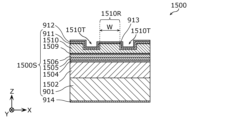
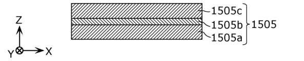


Classifications
-
- H—ELECTRICITY
- H01—ELECTRIC ELEMENTS
- H01S—DEVICES USING THE PROCESS OF LIGHT AMPLIFICATION BY STIMULATED EMISSION OF RADIATION [LASER] TO AMPLIFY OR GENERATE LIGHT; DEVICES USING STIMULATED EMISSION OF ELECTROMAGNETIC RADIATION IN WAVE RANGES OTHER THAN OPTICAL
- H01S5/00—Semiconductor lasers
- H01S5/30—Structure or shape of the active region; Materials used for the active region
- H01S5/34—Structure or shape of the active region; Materials used for the active region comprising quantum well or superlattice structures, e.g. single quantum well [SQW] lasers, multiple quantum well [MQW] lasers or graded index separate confinement heterostructure [GRINSCH] lasers
- H01S5/343—Structure or shape of the active region; Materials used for the active region comprising quantum well or superlattice structures, e.g. single quantum well [SQW] lasers, multiple quantum well [MQW] lasers or graded index separate confinement heterostructure [GRINSCH] lasers in AIIIBV compounds, e.g. AlGaAs-laser, InP-based laser
Definitions
- This disclosure relates to nitride-based semiconductor light-emitting devices.
- Patent Documents 1 to 3 To increase the efficiency of nitride-based semiconductor light-emitting elements, for example, techniques for reducing the operating voltage are known (see, for example, Patent Documents 1 to 3).
- the invention described in Patent Document 1 aims to increase the light confinement coefficient in the active layer while reducing the operating voltage.
- the present disclosure aims to solve these problems and provide a highly efficient nitride-based semiconductor light-emitting device.
- one aspect of the nitride-based semiconductor light-emitting device is a nitride-based semiconductor light-emitting device that includes a semiconductor laminate and a P-side electrode disposed above the semiconductor laminate, and emits light from an end face in a direction perpendicular to the lamination direction of the semiconductor laminate, the semiconductor laminate having an N-type first cladding layer, an N-side guide layer disposed above the N-type first cladding layer, an active layer disposed above the N-side guide layer, including a well layer and a barrier layer, and having a quantum well structure, a P-side first guide layer disposed above the active layer, a P-side second guide layer disposed above the P-side first guide layer, and a P-type cladding layer disposed above the P-side second guide layer, the band gap energy of the P-side second guide layer is greater than the band gap energy of the N-side guide layer, the band gap energy of the N-side guide layer is equal to
- a nitride-based semiconductor light-emitting device that includes a semiconductor laminate and a P-side electrode disposed above the semiconductor laminate, and emits light from an end face in a direction perpendicular to the lamination direction of the semiconductor laminate, the semiconductor laminate comprising an N-type first cladding layer, an N-side guide layer disposed above the N-type first cladding layer, an active layer disposed above the N-side guide layer and including a well layer and a barrier layer, the active layer having a quantum well structure, a P-side guide layer disposed above the active layer, and a P-side electrode disposed above the P-side guide layer.
- the band gap energy of the P-side guide layer monotonically increasing with increasing distance from the active layer
- the P-side guide layer includes a portion whose band gap energy increases continuously with increasing distance from the active layer
- the average band gap energy of the P-side guide layer is equal to or greater than the average band gap energy of the N-side guide layer
- the band gap energy of the barrier layer is equal to or less than the minimum value of the band gap energies of the N-side guide layer and the P-side guide layer
- the P-side electrode contains Ag.
- yet another aspect of the nitride-based semiconductor light-emitting device is a nitride-based semiconductor light-emitting device that includes a semiconductor laminate and a P-side electrode disposed above the semiconductor laminate, and emits light from an end face in a direction perpendicular to the lamination direction of the semiconductor laminate, the semiconductor laminate having an N-type first cladding layer, an N-side guide layer disposed above the N-type first cladding layer, an active layer disposed above the N-side guide layer, including a well layer and a barrier layer, and having a quantum well structure, a P-side guide layer disposed above the active layer, and a P-type cladding layer disposed above the P-side guide layer, the band gap energy of the N-side guide layer monotonically increases with increasing distance from the active layer, the N-side guide layer includes a portion in which the band gap energy increases continuously with increasing distance from the active layer, the average band gap energy of the P-side guide layer is
- This disclosure makes it possible to provide a highly efficient nitride-based semiconductor light-emitting device.
- 1 is a schematic plan view showing an overall configuration of a nitride-based semiconductor light-emitting device according to a first embodiment.
- 1 is a schematic cross-sectional view showing an overall configuration of a nitride-based semiconductor light-emitting device according to a first embodiment.
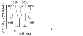
- 1 is a schematic cross-sectional view showing a configuration of an active layer included in a nitride-based semiconductor light-emitting element according to a first embodiment.
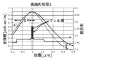
- 1 is a schematic diagram showing an overview of a light intensity distribution in a stacking direction of a nitride-based semiconductor light-emitting element according to a first embodiment.
- FIG. 3 is a graph showing coordinates of positions in a stacking direction of the nitride-based semiconductor light-emitting element according to the first embodiment.
- FIG. 1 is a diagram showing element structures used in simulations of the nitride-based semiconductor light-emitting elements of Comparative Examples 1 to 5 and the nitride-based semiconductor light-emitting element according to the first embodiment.
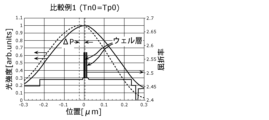
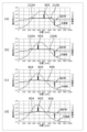
- 11 is a graph showing a simulation result of the light intensity distribution and the refractive index distribution in a portion below the ridge of the nitride-based semiconductor light-emitting element of Comparative Example 1.
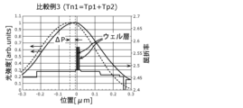
- FIG. 13 is a graph showing a simulation result of the light intensity distribution and the refractive index distribution in a portion below the ridge of the nitride-based semiconductor light-emitting element of Comparative Example 3.
- 4 is a graph showing a simulation result of the light intensity distribution and the refractive index distribution in a portion below the ridge of the nitride-based semiconductor light-emitting element according to the first embodiment.
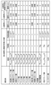
- FIG. 13 is a diagram showing numerical values obtained by simulation of each of the nitride-based semiconductor light-emitting devices of Comparative Examples 1 to 5 and the nitride-based semiconductor light-emitting device according to the first embodiment.
- FIG. 5 is a graph showing the relationship between the position in the width direction of the ridge and the amount of feedback of spontaneous emission light to an active layer by a P-side electrode according to the first embodiment.
- 4 is a first graph showing the relationship between the position in the width direction of the ridge and the amount of spontaneous emission light reabsorption by the active layer according to the first embodiment.
- 11 is a second graph showing the relationship between the position in the width direction of the ridge and the amount of spontaneous emission light reabsorption by the active layer according to the first embodiment.
- 4 is a graph showing the relationship between the ridge width and the amount of spontaneous emission light reabsorption by the active layer according to the first embodiment.
- FIG. 13 is a diagram showing the relationship between the film thickness of the P-type cladding layer of the nitride-based semiconductor light-emitting element of Comparative Example 5 and each numerical value obtained by simulation.
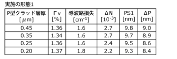
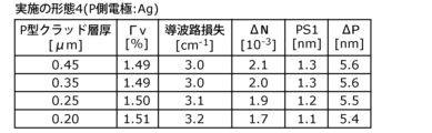
- 4 is a diagram showing the relationship between the film thickness of a P-type cladding layer of the nitride-based semiconductor light-emitting element according to the first embodiment and each numerical value obtained by simulation.
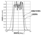
- FIG. 4 is a graph showing a simulation result of the relationship between the radiation angle and the light intensity of the nitride-based semiconductor light-emitting element according to the first embodiment.
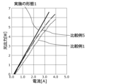
- 4 is a graph showing a simulation result of the IL characteristics of the nitride-based semiconductor light-emitting element according to the first embodiment.
- FIG. 1 is a schematic cross-sectional view showing an overall configuration of a nitride-based semiconductor light-emitting device according to a second embodiment.
- FIG. 11 is a schematic cross-sectional view showing an overall configuration of a nitride-based semiconductor light-emitting device according to a third embodiment.
- 11 is a cross-sectional view showing a configuration of an active layer included in a nitride-based semiconductor light-emitting element according to a third embodiment.
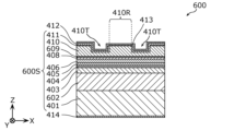
- FIG. FIG. 11 is a schematic cross-sectional view showing an overall configuration of a nitride-based semiconductor light-emitting device according to a fourth embodiment.
- FIG. 11 is a cross-sectional view showing a configuration of an active layer included in a nitride-based semiconductor light-emitting element according to a fourth embodiment.
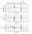
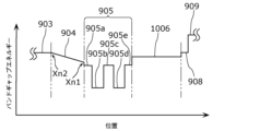
- FIG. 13 is a schematic graph showing the distribution of band gap energy of an active layer and each layer in the vicinity thereof of a nitride-based semiconductor light-emitting element according to a fourth embodiment. 13 is a graph showing the refractive index distribution and the light intensity distribution in the stacking direction of the nitride-based semiconductor light-emitting devices of Comparative Examples 7 to 9 and the nitride-based semiconductor light-emitting device according to the fourth embodiment.
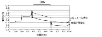
- FIG. 13 is a graph showing simulation results of distributions of valence electron charge potentials and hole Fermi levels in the stacking direction of the nitride-based semiconductor light-emitting devices of Comparative Examples 7 to 9 and the nitride-based semiconductor light-emitting device according to the fourth embodiment.
- 13 is a graph showing simulation results of the distribution of carrier concentration in the stacking direction of the nitride-based semiconductor light-emitting devices of Comparative Examples 7 to 9 and the nitride-based semiconductor light-emitting device according to the fourth embodiment.
- FIG. 13 is a diagram showing the relationship between the film thickness of the P-type cladding layer of the nitride-based semiconductor light-emitting element of Comparative Example 11 and each numerical value obtained by simulation.
- FIG. 13 is a diagram showing the relationship between the film thickness of a P-type cladding layer of a nitride-based semiconductor light-emitting element according to a fourth embodiment and each numerical value obtained by simulation.
- FIG. 13 is a schematic cross-sectional view showing an overall configuration of a nitride-based semiconductor light-emitting device according to a fifth embodiment.
- 13 is a schematic graph showing the distribution of band gap energy of an active layer and each layer in the vicinity thereof of a nitride-based semiconductor light-emitting element according to a fifth embodiment.
- FIG. 13 is a graph showing a simulation result of the distribution of valence electron charge potential and hole Fermi level in the stacking direction of the nitride-based semiconductor light-emitting element according to the fifth embodiment. 13 is a graph showing a simulation result of the distribution of carrier concentration in the stacking direction of the nitride-based semiconductor light-emitting element according to the fifth embodiment.
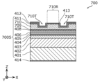
- FIG. 13 is a schematic cross-sectional view showing the overall configuration of a nitride-based semiconductor light-emitting device according to a sixth embodiment.
- FIG. 13 is a schematic cross-sectional view showing an overall configuration of a nitride-based semiconductor light-emitting device according to a seventh embodiment.
- FIG. 13 is a schematic cross-sectional view showing the overall configuration of a nitride-based semiconductor light-emitting device according to an eighth embodiment.
- FIG. 13 is a graph showing the distribution of the Al composition ratio in the stacking direction of an electron barrier layer according to the eighth embodiment.
- FIG. 13 is a schematic cross-sectional view showing an overall configuration of a nitride-based semiconductor light-emitting device according to a ninth embodiment.
- 13 is a schematic cross-sectional view showing a configuration of an active layer included in a nitride-based semiconductor light-emitting device according to a ninth embodiment.
- FIG. 23 is a schematic graph showing the distribution of band gap energy of an active layer and each layer in the vicinity thereof of a nitride-based semiconductor light-emitting element according to a ninth embodiment.
- 13 is a graph showing the refractive index distribution and the light intensity distribution in the stacking direction of the nitride-based semiconductor light-emitting devices of Comparative Examples 12 to 14 and the nitride-based semiconductor light-emitting device according to the ninth embodiment.
- 13 is a graph showing simulation results of distributions of valence electron charge potentials and hole Fermi levels in the stacking direction of the nitride-based semiconductor light-emitting devices of Comparative Examples 12 to 14 and the nitride-based semiconductor light-emitting device according to the ninth embodiment.
- 13 is a graph showing simulation results of the distribution of carrier concentration in the stacking direction of the nitride-based semiconductor light-emitting devices of Comparative Examples 12 to 14 and the nitride-based semiconductor light-emitting device according to the ninth embodiment. 13 is a graph showing the relationship between the position in the stacking direction of the nitride-based semiconductor light-emitting element of Comparative Example 14 and the piezoelectric polarization charge density, the piezoelectric polarization electric field, and the conduction field potential.
- FIG. 13 is a graph showing the relationship between the position in the stacking direction of the nitride-based semiconductor light-emitting element according to the ninth embodiment and the piezoelectric polarization charge density, the piezoelectric polarization electric field, and the conduction field potential.
- FIG. 13 is a diagram showing the relationship between the film thickness of the P-type cladding layer of the nitride-based semiconductor light-emitting element of Comparative Example 15 and each numerical value obtained by simulation.
- FIG. 13 is a diagram showing the relationship between the film thickness of a P-type cladding layer 910 of a nitride-based semiconductor light-emitting device 900 according to the ninth embodiment and each numerical value obtained by simulation.
- FIG. 13 is a schematic cross-sectional view showing the overall configuration of a nitride-based semiconductor light-emitting device according to a tenth embodiment.
- FIG. 23 is a schematic graph showing the distribution of band gap energy of an active layer and each layer in the vicinity thereof of a nitride-based semiconductor light-emitting element according to a tenth embodiment.
- FIG. 13 is a diagram showing the relationship between the film thickness of the P-type cladding layer of the nitride-based semiconductor light-emitting element of Comparative Example 16 and each numerical value obtained by simulation.
- FIG. 23 is a schematic graph showing the distribution of band gap energy of an active layer and each layer in the vicinity thereof of a nitride-based semiconductor light-emitting element according to a tenth embodiment.
- FIG. 13 is a diagram showing the relationship between the film thickness of the P-type cladding layer of the nitride-based semiconductor light-emitting element of Comparative Example 16 and each numerical value
- FIG. 23 is a diagram showing the relationship between the film thickness of a P-type cladding layer 910 of a nitride-based semiconductor light-emitting device according to the tenth embodiment and each numerical value obtained by simulation.
- 13 is a schematic cross-sectional view showing the overall configuration of a nitride-based semiconductor light-emitting device according to an eleventh embodiment.
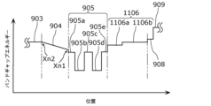
- FIG. 23 is a schematic graph showing the distribution of band gap energy of an active layer and each layer in the vicinity thereof of a nitride-based semiconductor light-emitting element according to an eleventh embodiment.
- FIG. 13 is a diagram showing the relationship between the film thickness of the P-type cladding layer of the nitride-based semiconductor light-emitting element of Comparative Example 17 and each numerical value obtained by simulation.
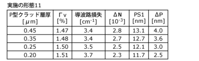
- FIG. 23 is a diagram showing the relationship between the film thickness of the P-type cladding layer of the nitride-based semiconductor light-emitting element according to the eleventh embodiment and each numerical value obtained by simulation.
- FIG. 23 is a schematic cross-sectional view showing the overall configuration of a nitride-based semiconductor light-emitting device according to a twelfth embodiment.
- FIG. 23 is a schematic graph showing the distribution of band gap energy of an active layer and each layer in the vicinity thereof of a nitride-based semiconductor light-emitting element according to a twelfth embodiment.
- FIG. 23 is a schematic cross-sectional view showing the overall configuration of a nitride-based semiconductor light-emitting device according to a thirteenth embodiment.
- FIG. 23 is a schematic cross-sectional view showing the overall configuration of a nitride-based semiconductor light-emitting device according to a fourteenth embodiment.
- 23 is a schematic graph showing the distribution of band gap energy in an active layer and each layer in the vicinity thereof of a nitride-based semiconductor light-emitting element according to a fourteenth embodiment.
- FIG. 23 is a schematic cross-sectional view showing the overall configuration of a nitride-based semiconductor light-emitting device according to a fifteenth embodiment.
- FIG. 23 is a schematic cross-sectional view showing a configuration of an active layer included in a nitride-based semiconductor light-emitting device according to a fifteenth embodiment.
- 23 is a schematic graph showing the distribution of band gap energy of an active layer and each layer in the vicinity thereof of a nitride-based semiconductor light-emitting device according to a fifteenth embodiment.
- 23 is a schematic graph showing the distribution of band gap energy of an active layer and each layer in the vicinity thereof in a nitride-based semiconductor light-emitting device according to Modification 1 of the fifteenth embodiment.
- FIG. 23 is a schematic graph showing the distribution of band gap energy of an active layer and each layer in the vicinity thereof in a nitride-based semiconductor light-emitting device according to Modification 2 of the fifteenth embodiment.
- 1 is a schematic cross-sectional view showing an overall configuration of a nitride-based semiconductor light-emitting device according to Modification 1.
- FIG. 11 is a schematic cross-sectional view showing an overall configuration of a nitride-based semiconductor light-emitting device according to Modification 2.
- each figure is a schematic diagram and is not necessarily an exact illustration. Therefore, the scale and the like are not necessarily the same in each figure. Furthermore, in each figure, the same reference numerals are used for substantially the same configuration, and duplicate explanations are omitted or simplified.
- the terms “above” and “below” do not refer to vertically above and below in an absolute spatial sense, but are used as terms defined by a relative positional relationship based on the stacking order in a stacked configuration. Furthermore, the terms “above” and “below” are applied not only to cases where two components are arranged with a gap between them and another component exists between the two components, but also to cases where two components are arranged in contact with each other.
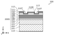
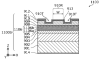
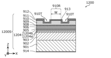
- FIGS. 1 and 2A are a schematic plan view and a cross-sectional view, respectively, showing the overall configuration of the nitride-based semiconductor light-emitting device 100 according to the present embodiment.
- FIG. 2A shows a cross section taken along line IIA-IIA in FIG. 1.
- FIG. 2B is a schematic cross-sectional view showing the configuration of the active layer 105 included in the nitride-based semiconductor light-emitting device 100 according to the present embodiment.
- Each figure shows an X-axis, a Y-axis, and a Z-axis that are orthogonal to each other.
- the X-axis, the Y-axis, and the Z-axis are in a right-handed Cartesian coordinate system.
- the stacking direction of the nitride-based semiconductor light-emitting device 100 is parallel to the Z-axis direction, and the main emission direction of light (laser light) is parallel to the Y-axis direction.
- the nitride-based semiconductor light-emitting element 100 includes a semiconductor stack 100S including a nitride-based semiconductor layer, and emits light from an end face 100F (see FIG. 1) perpendicular to the stacking direction (i.e., the Z-axis direction) of the semiconductor stack 100S.
- the nitride-based semiconductor light-emitting element 100 emits light in the 445 nm wavelength band.
- the nitride-based semiconductor light-emitting element 100 is a semiconductor laser element having two end faces 100F and 100R that form a resonator.
- the end face 100F is a front end face that emits laser light
- the end face 100R is a rear end face that has a higher reflectivity than the end face 100F.
- the reflectivities of the end faces 100F and 100R are 16% and 95%, respectively.
- the cavity length of the nitride-based semiconductor light-emitting element 100 according to this embodiment i.e., the distance between end face 100F and end face 100R is approximately 1200 ⁇ m.
- the nitride-based semiconductor light-emitting element 100 includes a semiconductor laminate 100S, a current blocking layer 112, a P-side electrode 113, and an N-side electrode 114.
- the semiconductor laminate 100S includes a substrate 101, an N-type first cladding layer 102, an N-type second cladding layer 103, an N-side guide layer 104, an active layer 105, a P-side first guide layer 106, a P-side second guide layer 107, an intermediate layer 108, an electron barrier layer 109, a P-type cladding layer 110, and a contact layer 111.
- the substrate 101 is a plate-like member that serves as the base for the nitride-based semiconductor light-emitting element 100.
- the substrate 101 is an N-type GaN substrate.
- the N-type first cladding layer 102 is an example of an N-type cladding layer disposed above the substrate 101.
- the N-type first cladding layer 102 is a layer having a smaller refractive index and a larger band gap energy than the active layer 105.
- the N-type first cladding layer 102 is an N-type Al 0.035 Ga 0.965 N layer having a film thickness of 1200 nm.
- the N-type first cladding layer 102 is doped with Si as an impurity at a concentration of 1 ⁇ 10 18 cm -3 .
- the N-type second cladding layer 103 is an example of an N-type cladding layer disposed above the substrate 101.
- the N-type second cladding layer 103 is disposed above the N-type first cladding layer 102.
- the N-type second cladding layer 103 is a layer having a smaller refractive index and a larger band gap energy than the active layer 105.
- the N-type second cladding layer 103 is an N-type GaN layer having a film thickness of 100 nm.
- the N-type second cladding layer 103 is doped with Si as an impurity at a concentration of 1 ⁇ 10 18 cm -3 .
- the N-side guide layer 104 is an optical guide layer disposed above the N-type second cladding layer 103.
- the N-side guide layer 104 has a higher refractive index and a smaller band gap energy than the N-type first cladding layer 102 and the N-type second cladding layer 103.
- the N-side guide layer 104 is an undoped In 0.04 Ga 0.96 N layer having a film thickness of 160 nm.
- the active layer 105 is disposed above the N-side guide layer 104 and is a light-emitting layer having a quantum well structure.
- the active layer 105 has well layers 105b and 105d and barrier layers 105a, 105c, and 105e, as shown in FIG. 2B.
- the barrier layer 105a is disposed above the N-side guide layer 104 and functions as a barrier for the quantum well structure.
- the barrier layer 105a is an undoped In 0.05 Ga 0.95 N layer having a thickness of 7 nm.
- the well layer 105b is disposed above the barrier layer 105a and functions as a well of the quantum well structure.
- the well layer 105b is disposed between the barrier layer 105a and the barrier layer 105c .
- the well layer 105b is an undoped In0.18Ga0.82N layer having a thickness of 3 nm.
- the barrier layer 105c is disposed above the well layer 105b and functions as a barrier for the quantum well structure.
- the barrier layer 105c is an undoped In0.05Ga0.95N layer having a thickness of 7 nm.
- the well layer 105d is disposed above the barrier layer 105c and functions as a well of the quantum well structure.
- the well layer 105d is disposed between the barrier layer 105c and the barrier layer 105e .
- the well layer 105d is an undoped In0.18Ga0.82N layer having a thickness of 3 nm.
- the barrier layer 105e is disposed above the well layer 105d and functions as a barrier for the quantum well structure.
- the barrier layer 105e is an undoped In0.05Ga0.95N layer having a thickness of 5 nm.
- the P-side first guide layer 106 is an optical guide layer disposed above the active layer 105.
- the P-side first guide layer 106 has a higher refractive index and a smaller band gap energy than the P-type cladding layer 110.
- the P-side first guide layer 106 is an undoped In 0.045 Ga 0.955 N layer with a film thickness of 80 nm.
- the P-side second guide layer 107 is an optical guide layer disposed above the P-side first guide layer 106.
- the P-side second guide layer 107 has a higher refractive index and a smaller band gap energy than the P-type cladding layer 110.
- the P-side second guide layer 107 is an undoped In 0.01 Ga 0.99 N layer having a film thickness of 195 nm.
- the intermediate layer 108 is a layer disposed above the active layer 105.
- the intermediate layer 108 is disposed between the P-side second guide layer 107 and the electron barrier layer 109, and reduces stress caused by the difference in lattice constant between the P-side second guide layer 107 and the electron barrier layer 109. This makes it possible to suppress the occurrence of crystal defects in the nitride-based semiconductor light-emitting element 100.
- the intermediate layer 108 is an undoped GaN layer with a thickness of 20 nm.
- the electron barrier layer 109 is disposed above the active layer 105 and is a nitride-based semiconductor layer containing at least Al. In this embodiment, the electron barrier layer 109 is disposed between the intermediate layer 108 and the P-type cladding layer 110.
- the electron barrier layer 109 is a P-type AlGaN layer having a thickness of 5 nm.
- the electron barrier layer 109 has an Al composition ratio gradient region in which the Al composition ratio monotonically increases as it approaches the P-type cladding layer 110.
- the configuration in which the Al composition ratio monotonically increases also includes a configuration including a region in which the Al composition ratio is constant in the stacking direction.
- the configuration in which the Al composition ratio monotonically increases also includes a configuration in which the Al composition ratio increases stepwise.
- the entire electron barrier layer 109 is an Al composition ratio increasing region, and the Al composition ratio increases at a constant rate of change in the stacking direction.
- the electron barrier layer 109 has a composition expressed as Al 0.02 Ga 0.98 N near the interface with the intermediate layer 108, and the Al composition ratio increases monotonically toward the P-type cladding layer 110, and has a composition expressed as Al 0.36 Ga 0.64 N near the interface with the P-type cladding layer 110.
- the electron barrier layer 109 is doped with Mg as an impurity at a concentration of 1 ⁇ 10 19 cm -3 .
- the electron barrier layer 109 can suppress the leakage of electrons from the active layer 105 to the P-type cladding layer 110.
- the electron barrier layer 109 has an Al composition ratio increasing region where the Al composition ratio increases monotonically, the potential barrier of the valence band of the electron barrier layer 109 can be reduced more than when the Al composition ratio is uniform. Therefore, holes can easily flow from the P-type cladding layer 110 to the active layer 105. Therefore, even when the total film thickness of the P-side first guide layer 106 and the P-side second guide layer 107, which are undoped layers, is large as in this embodiment, the increase in the electrical resistance of the nitride-based semiconductor light-emitting element 100 can be suppressed.
- the nitride-based semiconductor light-emitting element 100 can operate at a high output.
- the P-type cladding layer 110 is a P-type cladding layer disposed above the active layer 105.
- the P-type cladding layer 110 is disposed between the electron barrier layer 109 and the contact layer 111.
- the P-type cladding layer 110 is a layer having a smaller refractive index and a higher band gap energy than the active layer 105.
- the thickness of the P-type cladding layer 110 may be 460 nm or less. This can suppress the electrical resistance of the nitride-based semiconductor light-emitting device 100. Therefore, the operating voltage of the nitride-based semiconductor light-emitting device 100 can be reduced.
- the nitride-based semiconductor light-emitting device 100 since the self-heating during the operation of the nitride-based semiconductor light-emitting device 100 can be reduced, the temperature characteristics of the nitride-based semiconductor light-emitting device 100 can be improved. Therefore, the nitride-based semiconductor light-emitting device 100 can operate at a high output.
- the thickness of the P-type cladding layer 110 in order for the P-type cladding layer 110 to fully function as a cladding layer, the thickness of the P-type cladding layer 110 may be 200 nm or more. The thickness of the P-type cladding layer 110 may be 250 nm or more.
- the P-type cladding layer 110 is a P-type Al 0.035 Ga 0.965 N layer having a thickness of 450 nm.
- the P-type cladding layer 110 is doped with Mg as an impurity.
- the impurity concentration at the end of the P-type cladding layer 110 closer to the active layer 105 is lower than the impurity concentration at the end farther from the active layer 105.
- the P-type cladding layer 110 has a P-type Al 0.035 Ga 0.965 N layer doped with Mg to a concentration of 2 ⁇ 10 18 cm -3 and having a thickness of 150 nm, which is located on the side closer to the active layer 105, and a P-type Al 0.035 Ga 0.965 N layer doped with Mg to a concentration of 1 ⁇ 10 19 cm -3 and having a thickness of 300 nm, which is located on the side farther from the active layer 105.
- a ridge 110R is formed in the P-type cladding layer 110 of the nitride-based semiconductor light-emitting element 100.
- Two grooves 110T are formed in the P-type cladding layer 110, which are arranged along the ridge 110R and extend in the Y-axis direction.
- the ridge width W is about 30 ⁇ m.
- the distance between the lower end of the ridge 110R (i.e., the bottom of the groove 110T) and the active layer 105 is dp.
- the film thickness of the P-type cladding layer 110 at the lower end of the ridge 110R (i.e., the distance between the lower end of the ridge 110R and the interface between the P-type cladding layer 110 and the electron barrier layer 109) is dc.
- the contact layer 111 is disposed above the P-type cladding layer 110 and is in ohmic contact with the P-side electrode 113.
- the contact layer 111 is a P-type GaN layer having a thickness of 100 nm.
- the contact layer 111 is doped with Mg as an impurity at a concentration of 1 ⁇ 10 20 cm ⁇ 3 .
- the current blocking layer 112 is disposed above the P-type cladding layer 110, and is an insulating layer that is transparent to light from the active layer 105.
- the current blocking layer 112 is disposed in a region of the upper surface of the P-type cladding layer 110 other than the upper surface of the ridge 110R.
- the current blocking layer 112 is a SiO2 layer.
- the P-side electrode 113 is a conductive layer disposed above the semiconductor laminate 100S. In this embodiment, the P-side electrode 113 is disposed above the contact layer 111 and the current blocking layer 112, and is in contact with the contact layer 111.
- the P-side electrode 113 contains Ag.
- Ag which has a low refractive index for light in the 445 nm wavelength band, for at least a portion of the P-side electrode 113 on the contact layer 111, it is possible to reduce the seepage of light propagating through the waveguide into the P-side electrode 113, thereby reducing the waveguide loss that occurs in the P-side electrode 113.
- Ag has a refractive index of 0.5 or less in the wavelength range of 325 nm to 1500 nm, and a refractive index of 0.2 or less in the wavelength range of 360 nm to 950 nm.
- the spontaneous emission light emitted from the active layer 105 can be reflected with high reflectivity by the P-side electrode 113 and fed back to the active layer 105.
- the spontaneous emission light components fed back to the active layer 105 components with wavelengths shorter than the laser oscillation wavelength are reabsorbed in the active layer 105 to generate electron-hole pairs, which can be used again as electron-hole pairs for laser oscillation.
- the quantum efficiency of the electrons and holes injected into the active layer 105 contributing to laser oscillation is improved, the oscillation threshold is reduced, and the slope efficiency is improved.
- the thickness of the P-type cladding layer 110 can be made thin without causing a large increase in waveguide loss.
- the optical path length through the P-type cladding layer 110 which has a large free carrier absorption, is shortened in the spontaneous emission light that is emitted in the active layer 105, reflected by the P-side electrode 113, and returned to the active layer 105, and the attenuation of the spontaneous emission light in the P-type cladding layer 110 is reduced, and the feedback amount of the spontaneous emission light to the active layer 105 is increased.
- the quantum efficiency and slope efficiency can be further increased.
- the thickness of the P-side electrode 113 should be 100 nm or more. In addition, it is preferable to form the thickness to 500 nm or less in order to ensure the ease of the resist lift-off process when forming the electrode.
- the Ag film contained in the P-side electrode 113 is fabricated in contact with the contact layer 111, but the P-side electrode 113 may contain other metals (hereinafter also referred to as interface region metals) with a thickness of 5 nm or less in the interface region with the contact layer 111, such as Cr, Ti, Ni, Pd, Pt, and Au.
- interface region metals other metals (hereinafter also referred to as interface region metals) with a thickness of 5 nm or less in the interface region with the contact layer 111, such as Cr, Ti, Ni, Pd, Pt, and Au.
- the film thickness of the interface region metal is set to 3 nm or less, the decrease in reflectance of the Ag film can be further suppressed.
- the N-side electrode 114 is a conductive layer disposed below the substrate 101 (i.e., on the principal surface of the substrate 101 opposite the principal surface of the semiconductor laminate 100S on which the components other than the substrate 101 are disposed).
- the N-side electrode 114 is, for example, a single layer or a multilayer film formed of at least one of Cr, Ti, Ni, Pd, Pt, and Au.
- the nitride-based semiconductor light-emitting element 100 generates an effective refractive index difference ⁇ N between the portion below the ridge 110R and the portion below the groove 110T, as shown in FIG. 2A. This allows the light generated in the portion of the active layer 105 below the ridge 110R to be confined in the horizontal direction (i.e., the X-axis direction).
- FIG. 3 is a schematic diagram showing an overview of the light intensity distribution in the stacking direction of the nitride-based semiconductor light-emitting element 100 according to this embodiment.
- FIG. 3 shows a schematic cross-sectional view of the nitride-based semiconductor light-emitting element 100 and a graph showing an overview of the light intensity distribution in the stacking direction at positions corresponding to each of the ridge 110R and the groove 110T.
- the light intensity distribution in the stacking direction depends on the stacking structure, and the peak of the light intensity distribution is not necessarily located in the active layer.
- the stacking structure of the nitride-based semiconductor light-emitting device 100 according to this embodiment is different in the part below the ridge 110R and the part below the groove 110T, the light intensity distribution is also different in the part below the ridge 110R and the part below the groove 110T.
- the peak position of the light intensity distribution in the stacking direction at the center in the horizontal direction (i.e., the X-axis direction) of the part below the ridge 110R is PS1.
- FIG. 4 is a graph showing the coordinates of positions in the stacking direction of the nitride-based semiconductor light-emitting device 100 according to this embodiment. As shown in FIG.
- the coordinate of the position in the stacking direction of the N-side end face of the well layer 105b, 105d, that is, the end face of the well layer 105b closest to the N-side guide layer 104, that is, the end face of the well layer 105b closer to the N-side guide layer 104, is set to zero
- the downward direction (the direction toward the N-side guide layer 104) is set to the negative direction of the coordinate
- the upward direction (the direction toward the P-side first guide layer 106) is set to the positive direction of the coordinate.
- the absolute value of the difference between positions PS1 and PS2 is set to the peak position difference ⁇ P.
- the thickness of the P-type cladding layer 110 is set to be relatively thin in order to reduce the operating voltage. Accordingly, the height of the ridge 110R (i.e., the height of the ridge 110R from the bottom surface of the groove 110T) is also set to be relatively low.
- the peak position of the light intensity distribution in the stacking direction shifts in a direction approaching the N-type cladding layer from the active layer. Therefore, the light confinement coefficient in the active layer decreases, and the thermal saturation level of the light output decreases accordingly. Therefore, it becomes difficult to operate the semiconductor light-emitting device at high output.
- the band gap energy of the P-side second guide layer 107 is larger than the band gap energy of the N-side guide layer 104, and the band gap energy of the N-side guide layer 104 is equal to or larger than the band gap energy of the P-side first guide layer 106.
- the thickness of the P-side first guide layer 106 is Tp1
- the thickness of the P-side second guide layer 107 is Tp2
- the thickness of the N-side guide layer 104 is Tn1
- the band gap energy of the N-side guide layer 104 is equal to or greater than the band gap energy of the P-side first guide layer 106.
- the P-side first guide layer 106 is made of InXp1Ga1 -Xp1N
- the N-side guide layer 104 is made of InXn1Ga1 -Xn1N , Xn1 ⁇ Xp1 (2) Therefore, the refractive index of the N-side guide layer 104 is equal to or lower than the refractive index of the P-side first guide layer 106.
- the In composition ratios Xn1 and Xp1 of the N-side guide layer 104 and the P-side first guide layer 106 are as follows: Xn1 ⁇ Xp1 (3) The relationship is satisfied. More specifically, the N-side guide layer 104 is an In 0.04 Ga 0.96 N layer, and the P-side first guide layer 106 is an In 0.045 Ga 0.955 N layer.
- the band gap energy of the N-side guide layer 104 is larger than the band gap energy of the P-side first guide layer 106.
- the refractive index of the N-side guide layer 104 is smaller than the refractive index of the P-side first guide layer 106.
- the light intensity distribution can be moved in a direction approaching the P-side first guide layer 106 from the active layer 105.
- the sum of the thickness Tp1 of the P-side first guide layer 106 and the thickness Tp2 of the P-side second guide layer 107 is greater than the thickness Tn1 of the N-side guide layer 104.
- the light intensity distribution can be moved from the active layer 105 toward the P-side first guide layer 106, compared to when the sum of the thicknesses of the P-side first guide layer 106 and the P-side second guide layer 107 is equal to or less than the thickness Tn1 of the N-side guide layer 104.
- the band gap energy of the P-side second guide layer 107 is greater than the band gap energy of the N-side guide layer 104.
- the refractive index of the P-side second guide layer 107 is smaller than the refractive index of the N-side guide layer 104. This makes it possible to prevent the light intensity distribution from moving too far in the direction approaching the P-type cladding layer 110 from the active layer 105.
- the band gap energy of the P-side second guide layer 107 is larger than the band gap energy of the N-side guide layer 104.
- the P-side second guide layer 107 is made of InXp2Ga1 -Xp2N
- the In composition ratio Xp2 of the P-side second guide layer 107 and the In composition ratio Xn1 of the N-side guide layer 104 are as follows: Xp2 ⁇ Xn1 (4) The relationship is satisfied.
- the N-side guide layer 104 is an In 0.04 Ga 0.96 N layer
- the P-side second guide layer 107 is an In 0.01 Ga 0.99 N layer.
- the refractive index of the N-side guide layer 104 is greater than the refractive index of the P-side second guide layer 107. This makes it possible to suppress the light intensity distribution from moving too far in the direction approaching the P-type cladding layer 110 from the active layer 105.
- the barrier layers 105a, 105c, and 105e of the active layer 105 are made of InXbGa1 -XbN , and the In composition ratios Xb and Xp1 of the barrier layers and the P-side first guide layer 106 are as follows: Xp1 ⁇ Xb (5) This satisfies the relationship below.
- the refractive index of each barrier layer can be made larger than those of the P-side first guide layer 106 and the N-side guide layer 104. This allows the peak of the light intensity distribution in the stacking direction to be positioned in the active layer 105. In addition, it is possible to suppress the light intensity distribution from moving too far in a direction approaching the P-type cladding layer 110 from the active layer 105.
- the average refractive index of the P-side first guide layer 106 and the P-side second guide layer 107 is smaller than the average refractive index of the N-side guide layer 104. This makes it possible to prevent the light intensity distribution from moving too far in the direction approaching the P-type cladding layer 110 from the active layer 105.
- the thicknesses Tp1 and Tp2 of the P-side first guide layer 106 and the P-side second guide layer 107 are as follows: Tp1 ⁇ Tp2 (6) The relationship is satisfied. In this way, by making the thickness of the P-side first guide layer 106, which has a small band gap energy, i.e., a large refractive index, relatively small, it is possible to suppress the light intensity distribution from moving too far in the direction approaching the P-type cladding layer 110 from the active layer 105.
- the thickness of the P-side first guide layer 106 which has a small In composition ratio, relatively small, it is possible to avoid arranging the P-side first guide layer 106, which has a small In composition ratio and a large thickness, in the vicinity of the upper part of the well layers 105b and 105d, which have the largest In composition ratio in the semiconductor laminate 100S. Therefore, it is possible to suppress the occurrence of lattice defects.
- the thicknesses Tp1 and Tn1 of the P-side first guide layer 106 and the N-side guide layer 104 are defined as follows: Tp1 ⁇ Tn1 (7)
- Tp1 ⁇ Tn1 (7) the film thickness of the P-side first guide layer 106, which has a small band gap energy, i.e., a large refractive index, smaller than the film thickness of the N-side guide layer 104, it is possible to suppress the light intensity distribution from moving too far in the direction approaching the P-type cladding layer 110 from the active layer 105.
- the band gap energy of the N-type second cladding layer 103 is smaller than the band gap energy of the N-type first cladding layer 102 and larger than the band gap energy of the P-side second guide layer 107.
- the N-type second cladding layer 103 which has a smaller band gap energy than the N-type first cladding layer 102, i.e., a larger refractive index, between the N-type first cladding layer 102 and the N-side guide layer 104, it is possible to suppress the light intensity distribution from moving too far in the direction approaching the P-type cladding layer 110 from the active layer 105.
- the band gap energy of the N-type second cladding layer 103 is made larger than the band gap energy of the P-side second guide layer 107, it is possible to suppress the light intensity distribution from moving too far from the active layer 105 to the N-type second cladding layer 103.
- the position PS1 of the peak of the light intensity distribution in the stacking direction in the portion below the ridge 110R can be set to 9.8 nm.
- the peak of the light intensity distribution can be positioned in the active layer 105.
- ⁇ P can be suppressed to 9.0 nm. This makes it possible to increase the light confinement coefficient in the active layer 105 to approximately 1.36%.
- the peak of the light intensity distribution in the stacking direction can be positioned in the active layer 105.
- the peak of the light intensity distribution in the stacking direction being positioned in the active layer 105 means that the peak of the light intensity distribution in the stacking direction is positioned in the active layer 105 at at least one position in the horizontal direction of the nitride-based semiconductor light-emitting device 100, and is not limited to the state in which the peak of the light intensity distribution in the stacking direction is positioned in the active layer 105 at all positions in the horizontal direction.
- the proportion of the portion of the light located in the P-type cladding layer 110 can be increased compared to when the peak of the light intensity distribution is located in the N-side guide layer 104.
- the P-type cladding layer 110 has a higher impurity concentration than the N-type first cladding layer 102 and the N-type second cladding layer 103, the proportion of the portion of the light located in the P-type cladding layer 110 increases, and there is a concern that the free carrier loss in the P-type cladding layer 110 will increase.
- the P-side first guide layer 106 and the P-side second guide layer 107 are undoped layers, and the sum of the thickness Tp1 of the P-side first guide layer 106 and the thickness Tp2 of the P-side second guide layer 107 is relatively large, so that the proportion of the portion of the light intensity distribution located in the undoped layer can be increased. Therefore, the increase in the free carrier loss can be suppressed. Specifically, in this embodiment, the waveguide loss can be suppressed to about 1.6 cm ⁇ 1 .
- the effective refractive index difference ⁇ N between the portion below the ridge 110R and the portion below the groove 110T is set to be relatively small.
- the effective refractive index difference ⁇ N is set by adjusting the distance dp (see FIG. 2A ) between the current blocking layer 112 and the active layer 105.
- the effective refractive index difference ⁇ N becomes smaller as the distance dp increases.
- the effective refractive index difference ⁇ N is about 2.4 ⁇ 10 ⁇ 3 .
- the number of higher-order modes i.e., higher-order transverse modes
- the number of higher-order modes that can propagate through the waveguide formed by the ridge 110R is smaller than when the effective refractive index difference ⁇ N is larger than 2.4 ⁇ 10 ⁇ 3 .
- the proportion of each higher-order mode among all the transverse modes included in the emitted light of the nitride-based semiconductor light-emitting device 100 becomes relatively large. Therefore, the increase or decrease in the number of modes and the change in the optical confinement factor in the active layer 105 due to inter-mode coupling become relatively large.
- the linearity of the characteristic of the optical output with respect to the supplied current decreases.
- a non-linear portion occurs in the graph showing the IL characteristic.
- the optical intensity distribution in the portion below the ridge 110R is dominated by the fundamental mode (i.e., the zeroth mode), and the optical intensity distribution in the portion below the groove 110T is dominated by higher modes.
- the peak of the light intensity distribution obtained by adding up the light intensity distributions in the portions below both the ridge 110R and the groove 110T moves to a position closer to position PS1. Therefore, the greater the difference ⁇ P between positions PS1 and PS2, the greater the fluctuation in the light confinement factor in the active layer 105 when the number of modes changes. Therefore, the stability of the light output decreases.
- the nitride-based semiconductor light-emitting device 100 includes the N-side guide layer 104 having the above-described configuration, and the P-side first guide layer 106 and the P-side second guide layer 107, so that the peak of the light intensity distribution can be positioned in the active layer 105 in both the portion below the ridge 110R and the portion below the groove 110T. In other words, the difference ⁇ P between the positions PS1 and PS2 of the peak of the light intensity distribution can be reduced.
- the distance dp is set to a relatively large value.
- the electron barrier layer 109 has a large band gap energy, so that the holes injected from the contact layer 111 tend to leak from the sidewall of the ridge 110R to the outside of the ridge 110R when passing through the electron barrier layer 109. As a result, the holes flow below the groove 110T.
- the light distribution intensity is small in the active layer 105 below the groove 110T, so the probability of radiative recombination of the electrons and holes injected into the active layer 105 decreases, and non-radiative recombination increases.
- the nitride-based semiconductor light-emitting element 100 is prone to deterioration.
- the lower end of the ridge 110R is set to be located above the electron barrier layer 109.
- the distance dc (see FIG. 2A) from the bottom end of the ridge 110R to the electron barrier layer 109 becomes too large, holes will flow from the ridge 110R into the gap between the groove 110T and the electron barrier layer 109, resulting in leakage current.
- the distance dc is set to the smallest possible value.
- FIG. 5 is a diagram showing the element structure used in the simulation of each of the nitride-based semiconductor light-emitting elements of Comparative Example 1 to Comparative Example 5 and the nitride-based semiconductor light-emitting element 100 according to the present embodiment.
- FIGS. 5 is a diagram showing the element structure used in the simulation of each of the nitride-based semiconductor light-emitting elements of Comparative Example 1 to Comparative Example 5 and the nitride-based semiconductor light-emitting element 100 according to the present embodiment.
- FIGS. 6 to 8 are graphs showing the simulation results of the light intensity distribution and the refractive index distribution in the portion below the ridge 110R of the nitride-based semiconductor light-emitting element of Comparative Example 1, Comparative Example 3, and the present embodiment, respectively.
- the horizontal axis of FIGS. 6 to 8 indicates the position in the stacking direction, and the vertical axis on the left and right indicates the light intensity and the refractive index, respectively.
- the light intensity distribution in the stacking direction in the portion below the groove 110T is also shown by a dotted line.
- FIG. 9 is a diagram showing numerical values obtained by simulation of each of the nitride-based semiconductor light-emitting devices of Comparative Examples 1 to 5 and the nitride-based semiconductor light-emitting device 100 according to the present embodiment.
- FIG. 9 shows the distance dc from the lower end of the ridge 110R to the electron barrier layer 109, the optical confinement factor, the waveguide loss, the effective refractive index difference ⁇ N, the peak position PS1 of the light intensity distribution in the stacking direction at the horizontal center of the lower part of the ridge 110R, and the absolute value ⁇ P of the difference between the peak position PS1 and the peak position PS2 in the stacking direction of the limit mode of wave-guiding.
- the distance dc is set to a distance that can make the effective refractive index difference 2.8 ⁇ 10 ⁇ 3 or less.
- the limit mode of wave-guiding means the highest order mode that can propagate in each nitride-based semiconductor light-emitting device.
- the peak position in the stacking direction of the limit mode of wave-guiding is a numerical value corresponding to the peak position of the light intensity distribution in the part below the groove 110T where the higher order mode is dominant.
- the nitride-based semiconductor light-emitting devices of Comparative Example 1 to Comparative Example 5 shown in FIG. 5 differ from the nitride-based semiconductor light-emitting device 100 according to the present embodiment in at least one of the configurations of the N-side guide layer and the P-side guide layer and the configuration of the P-side electrode.
- the nitride-based semiconductor light-emitting devices of Comparative Example 1 to Comparative Example 4 differ from the nitride-based semiconductor light-emitting device 100 according to the present embodiment in the configurations of the N-side guide layer and the P-side guide layer.
- the nitride-based semiconductor light-emitting device of Comparative Example 5 has the same configuration of the N-side guide layer and the P-side guide layer as the nitride-based semiconductor light-emitting device 100 according to the present embodiment. Furthermore, the nitride-based semiconductor light-emitting devices of Comparative Example 1, Comparative Example 3, and Comparative Example 5 differ from the nitride-based semiconductor light-emitting device 100 according to the present embodiment in the configuration of the P-side electrode. Specifically, the P-side electrode of the nitride-based semiconductor light-emitting devices of Comparative Example 1, Comparative Example 3, and Comparative Example 5 is made of Pd. On the other hand, the P-side electrode of the nitride-based semiconductor light-emitting devices of Comparative Example 2 and Comparative Example 4 contains Ag, like the P-side electrode of the present embodiment.
- the thickness Tn0 of the N-side guide layer is equal to the thickness Tp0 of the P-side guide layer.
- both the N-side guide layer and the P-side guide layer are In 0.03 Ga 0.97 N layers with a thickness of 220 nm.
- the nitride-based semiconductor light-emitting devices of Comparative Example 3 and Comparative Example 4 have an N-side guide layer, a P-side first guide layer, and a P-side second guide layer, similar to the nitride-based semiconductor light-emitting device 100 according to the present embodiment.
- the Al composition ratio of the electron barrier layers of Comparative Examples 1 to 5 and the electron barrier layer 109 of this embodiment is uniform. In other words, the Al composition ratio of each electron barrier layer is not inclined in the stacking direction.
- the film thickness of the N-side guide layer is equal to the film thickness of the P-side guide layer, so that the peak of the light intensity distribution is located in the active layer 105 below the ridge 110R. Therefore, the light confinement coefficient to the active layer 105 is high below the ridge 110R.
- the film thickness of the P-side guide layer is not large, so it is affected by the light intensity distribution of the current blocking layer 112 arranged in the groove 110T.
- the peak of the light intensity distribution in the stacking direction below the groove 110T is located in the N-side guide layer, so the light confinement coefficient is low below the groove 110T.
- the difference ⁇ P between the peak position of the light intensity distribution in the stacking direction below the ridge 110R and the peak position of the light intensity distribution in the stacking direction below the groove 110T is relatively large. Therefore, the linearity of the IL characteristics of the nitride-based semiconductor light-emitting device of Comparative Example 1 is low.
- the film thickness of the P-side second guide layer is smaller than that of the nitride-based semiconductor light-emitting device 100 according to the present embodiment, and therefore, as shown in FIG. 7, the effect on the light intensity distribution of the current blocking layer 112 is relatively large. For this reason, the difference ⁇ P between the peak position of the light intensity distribution in the stacking direction in the portion below the ridge 110R and the peak position of the light intensity distribution in the stacking direction in the portion below the groove 110T is relatively large. Therefore, the linearity of the IL characteristics of the nitride-based semiconductor light-emitting device of Comparative Example 3 is low.
- the sum of the thickness Tp1 of the P-side first guide layer 106 and the thickness Tp2 of the P-side second guide layer 107 is greater than the thickness Tn1 of the N-side guide layer 104, so that the effective refractive index difference ⁇ N can be reduced. Therefore, the horizontal spread angle of the emitted light can be reduced.
- the distance dc from the lower end of the ridge 110R to the electron barrier layer 109 can be set to 40 nm, which is significantly smaller than the distance dc in each comparative example. Therefore, the leakage current flowing between the lower end of the ridge 110R and the electron barrier layer 109 can be suppressed, and the oscillation threshold current value can be reduced.
- the peak of the light intensity distribution in the stacking direction can be positioned in the active layer 105 in both the portion below the ridge 110R and the portion below the groove 110T. Therefore, the light confinement factor can be increased compared to each comparative example. In addition, the difference ⁇ P in the peak positions can be reduced, thereby improving the linearity of the IL characteristics.
- the peak of the light intensity distribution in the stacking direction is located in the active layer 105, so the light intensity in the P-type cladding layer 110 is greater than in the case of the comparative example 3 in which the peak of the light intensity distribution is located in the N-side guide layer. For this reason, there is a concern that the free carrier loss in the P-type cladding layer 110, which has a higher impurity concentration than the N-type first cladding layer 102 and the N-type second cladding layer 103, will increase.
- the P-side first guide layer 106 and the P-side second guide layer 107 are undoped layers, and the sum of the thickness Tp1 of the P-side first guide layer 106 and the thickness Tp2 of the P-side second guide layer 107 is relatively large, so that the proportion of the portion of the light intensity distribution located in the undoped layer can be increased. Therefore, the increase in free carrier loss can be suppressed.
- the impurity concentration at the end of the P-type cladding layer 110 closer to the active layer 105 is lower than the impurity concentration at the end farther from the active layer 105, so that free carrier loss at the end of the P-type cladding layer 110 closer to the active layer 105, where the light intensity is relatively high, can be suppressed.
- the P-side electrode 113 contains Ag, the refractive index of the P-side electrode 113 can be reduced and the reflectance can be increased. Therefore, the leakage of light into the P-side electrode 113 can be suppressed, and the light loss in the P-side electrode 113 can be reduced.
- the reflectance of the P-side electrode 113 is high, of the spontaneous emission light generated in the active layer 105, a portion of the spontaneous emission light that is incident on the P-side electrode 113 is reflected by the P-side electrode 113 and returns to the active layer 105 (i.e., is fed back).
- This allows the active layer 105 to be optically excited, thereby increasing the ratio of the optical output to the input power of the nitride-based semiconductor light-emitting element 100.
- the efficiency of the nitride-based semiconductor light-emitting element 100 can be increased.
- the effect of the P-side electrode 113 on the spontaneous emission light will be explained using Figures 10 to 13.
- FIG. 10 is a graph showing the relationship between the position in the width direction (i.e., the X-axis direction) of the ridge 110R according to this embodiment and the amount of feedback of spontaneous emission light by the P-side electrode 113 to the active layer 105.
- FIG. 10 also shows a graph (dashed line) showing the amount of feedback when the P-side electrode is made of Pd, and a graph (dotted line) showing the amount of feedback by the N-side electrode 114 made of Ti.
- FIG. 11 is a first graph showing the relationship between the position in the width direction of the ridge 110R according to this embodiment and the amount of reabsorption of spontaneous emission light by the active layer 105.
- FIG. 11 shows the amount of reabsorption when the thickness Tpc of the P-type cladding layer 110 is 0.15 ⁇ m, 0.25 ⁇ m, 0.35 ⁇ m, and 0.45 ⁇ m.
- FIG. 11 also shows a graph when the P-side electrode is made of Pd and the thickness Tpc of the P-type cladding layer 110 is 0.45 ⁇ m.
- Fig. 12 is a second graph showing the relationship between the position in the width direction of the ridge 110R according to this embodiment and the amount of re-absorption of spontaneous emission light by the active layer 105.
- FIG. 12 shows the amount of re-absorption when the ridge width W is 3 ⁇ m, 15 ⁇ m, 30 ⁇ m, 45 ⁇ m, 60 ⁇ m, 90 ⁇ m, 120 ⁇ m, 200 ⁇ m, and 300 ⁇ m.
- the position where the horizontal axis in Figs. 10 to 12 is 0 ⁇ m indicates one end in the width direction of the ridge 110R.
- the position where the horizontal axis in Figs. 10 and 11 is 45 ⁇ m indicates the other end in the width direction of the ridge 110R.
- FIG. 13 is a graph showing the relationship between the ridge width W in this embodiment and the amount of spontaneous emission light reabsorption by the active layer 105.
- the amount of feedback of spontaneous emission light can be significantly increased compared to when the P-side electrode is made of Pd. Also, as shown in FIG. 10, the proportion of the feedback amount of spontaneous emission light from the P-side electrode 113 is overwhelmingly greater than that from the N-side electrode 114. Therefore, in order to increase the amount of feedback of spontaneous emission light, it is effective to increase the reflectance of spontaneous emission light at the P-side electrode 113, as in this embodiment.
- the reabsorption of spontaneously emitted light by the active layer 105 can be further increased.
- the ridge width W may be 30 ⁇ m or more. Furthermore, to further increase the amount of reabsorption of spontaneously emitted light, the ridge width W may be 40 ⁇ m or more. However, if the ridge width W becomes too large, the adverse effects of heat generation become significant, so the ridge width W may be 200 ⁇ m or less.
- Fig. 14 is a diagram showing the relationship between the film thickness of the P-type cladding layer of the nitride-based semiconductor light-emitting device of Comparative Example 5 and each numerical value obtained by simulation.
- Fig. 15 is a diagram showing the relationship between the film thickness of the P-type cladding layer 110 of the nitride-based semiconductor light-emitting device 100 according to this embodiment and each numerical value obtained by simulation.
- the film thickness of the P-type cladding layer 110 as a whole was changed to 0.45 ⁇ m, 0.35 ⁇ m, 0.25 ⁇ m, and 0.20 ⁇ m by changing the film thickness of the P-type Al 0.035 Ga 0.965 N layer doped with Mg at a concentration of 1 x 10 19 cm -3 in the P-type cladding layer 110.
- the P-side electrode 113 containing Ag by providing the P-side electrode 113 containing Ag, it is possible to suppress an increase in waveguide loss even if the P-type cladding layer 110 is thinned to about 200 nm.
- Fig. 16 is a graph showing a simulation result of the relationship between the radiation angle and the light intensity of the nitride-based semiconductor light-emitting element 100 according to the present embodiment.
- Fig. 16 also shows the relationship between the radiation angle and the light intensity of a nitride-based semiconductor light-emitting element having an effective refractive index difference ⁇ N of 7 ⁇ 10 -3 as Comparative Example 6.
- Fig. 17 is a graph showing a simulation result of the IL characteristics of the nitride-based semiconductor light-emitting element 100 according to the present embodiment.
- Fig. 17 also shows the IL characteristics of the nitride-based semiconductor light-emitting elements of Comparative Example 1 and Comparative Example 5.
- the effective refractive index difference ⁇ N is 2.7 ⁇ 10 ⁇ 3 , and therefore the beam divergence angle in the horizontal direction can be reduced more than in the nitride-based semiconductor light-emitting element of Comparative Example 6.
- the nitride-based semiconductor light-emitting device 100 has IL characteristics with higher linearity than the nitride-based semiconductor light-emitting devices of the respective comparative examples. In addition, it is possible to obtain a higher slope efficiency than the respective comparative examples.
- the thickness Tp2 of the P-side second guide layer 107 may be 100 nm or more, it is possible to simultaneously reduce the waveguide loss, increase the optical confinement factor ⁇ v, and reduce the effective refractive index difference ⁇ N. Furthermore, in order to further increase the optical confinement factor ⁇ v, the thickness Tp2 may be 250 nm or less. Furthermore, in order to position PS1 and PS2 in the vicinity of the well layers 105b and 105d of the active layer 105, the In composition ratio Xp2 of the P-side second guide layer 107 may be 0.5% or more.
- the nitride-based semiconductor light-emitting device according to the present embodiment differs from the nitride-based semiconductor light-emitting device 100 according to the first embodiment in the relationship of the Al composition ratio between the N-type first cladding layer and the P-type cladding layer.
- the nitride-based semiconductor light-emitting device according to the present embodiment will be described below with reference to FIG. 18, focusing on the differences from the nitride-based semiconductor light-emitting device 100 according to the first embodiment.
- the nitride-based semiconductor light-emitting device 200 includes a semiconductor laminate 200S, a current blocking layer 112, a P-side electrode 113, and an N-side electrode 114.
- the semiconductor laminate 200S includes a substrate 101, an N-type first cladding layer 202, an N-type second cladding layer 103, an N-side guide layer 104, an active layer 105, a P-side first guide layer 106, a P-side second guide layer 107, an intermediate layer 108, an electron barrier layer 109, a P-type cladding layer 210, and a contact layer 111.
- the N-type first cladding layer 202 is a 1200 nm-thick N-type Al 0.036 Ga 0.964 N layer.
- the N-type first cladding layer 202 is doped with Si as an impurity at a concentration of 1 ⁇ 10 18 cm ⁇ 3 .
- the P-type cladding layer 210 is a P-type Al 0.026 Ga 0.974 N layer having a thickness of 450 nm.
- the P-type cladding layer 210 is doped with Mg as an impurity.
- the impurity concentration at the end of the P-type cladding layer 210 closer to the active layer 105 is lower than the impurity concentration at the end farther from the active layer 105.
- the P-type cladding layer 210 has a P-type Al 0.026 Ga 0.974 N layer having a thickness of 150 nm and doped with Mg at a concentration of 2 ⁇ 10 18 cm ⁇ 3, which is disposed closer to the active layer 105, and a P-type Al 0.026 Ga 0.974 N layer having a thickness of 300 nm and doped with Mg at a concentration of 1 ⁇ 10 19 cm ⁇ 3, which is disposed farther from the active layer 105 .
- a ridge 210R is formed in the P-type cladding layer 210, similar to the P-type cladding layer 110 according to the first embodiment. Furthermore, two grooves 210T are formed in the P-type cladding layer 210, arranged along the ridge 210R and extending in the Y-axis direction.
- the nitride-based semiconductor light-emitting device 200 according to this embodiment also exhibits the same effects as the nitride-based semiconductor light-emitting device 100 according to the first embodiment.
- the N-type first cladding layer 202 and the P-type cladding layer 210 contain Al. If the Al composition ratios of the N-type first cladding layer 202 and the P-type cladding layer 210 are Ync and Ypc, respectively, then: Ync>Ypc (10) Satisfy the relationship.
- the composition ratios Ync and Ypc indicate the average Al composition ratio.
- the N-type first cladding layer 202 includes multiple 2 nm thick GaN layers and multiple 2 nm thick AlGaN layers with an Al composition ratio of 0.07, and the multiple GaN layers and the multiple AlGaN layers are alternately stacked, Ync is 0.035, which is the average Al composition ratio of the entire N-type first cladding layer 202.
- Ypc is 0.035, which is the average Al composition ratio of the entire P-type cladding layer 210.
- the refractive index of the N-type first cladding layer 202 allows the refractive index of the N-type first cladding layer 202 to be lower than that of the P-type cladding layer 210. Therefore, even if the thickness of the P-type cladding layer 210 is reduced to reduce the operating voltage of the nitride-based semiconductor light-emitting device 200, the refractive index of the N-type first cladding layer 202 is smaller than that of the P-type cladding layer 210, so that the peak of the light intensity distribution in the stacking direction can be prevented from moving in a direction approaching the N-type first cladding layer 202 from the active layer 105.
- FIG. 3 A nitride-based semiconductor light-emitting device according to embodiment 3 will be described.
- the nitride-based semiconductor light-emitting device according to this embodiment differs from the nitride-based semiconductor light-emitting device 200 according to embodiment 2 in the configuration of the active layer.
- the nitride-based semiconductor light-emitting device according to this embodiment will be described below with reference to Figures 19A and 19B, focusing on the differences from the nitride-based semiconductor light-emitting device 200 according to embodiment 2.
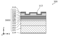
- FIG. 19A is a schematic cross-sectional view showing the overall configuration of a nitride-based semiconductor light-emitting device 300 according to this embodiment.
- FIG. 19B is a cross-sectional view showing the configuration of an active layer 305 included in the nitride-based semiconductor light-emitting device 300 according to this embodiment.
- the nitride-based semiconductor light-emitting device 300 includes a semiconductor laminate 300S, a current blocking layer 112, a P-side electrode 113, and an N-side electrode 114.
- the semiconductor laminate 300S includes a substrate 101, an N-type first cladding layer 202, an N-type second cladding layer 103, an N-side guide layer 104, an active layer 305, a P-side first guide layer 106, a P-side second guide layer 107, an intermediate layer 108, an electron barrier layer 109, a P-type cladding layer 210, and a contact layer 111.
- the active layer 305 has a single quantum well structure, and includes a single well layer 105b and barrier layers 105a and 105c sandwiching the well layer 105b.
- the well layer 105b has a similar structure to the well layer 105b according to the first embodiment
- the barrier layers 105a and 105c have a similar structure to the barrier layers 105a and 105c according to the first embodiment.
- the nitride-based semiconductor light-emitting device 300 has the same effect as the nitride-based semiconductor light-emitting device 200 according to the second embodiment.
- the active layer 305 has a single well layer 105b.
- the peak of the light intensity distribution in the stacking direction can be positioned in the active layer 305 or in its vicinity by the configuration of the N-side guide layer 104, the P-side first guide layer 106, the P-side second guide layer 107, etc. Therefore, the light confinement coefficient can be increased.
- Embodiment 4 A nitride-based semiconductor light-emitting device according to embodiment 4 will be described.
- the nitride-based semiconductor light-emitting device according to this embodiment differs from the nitride-based semiconductor light-emitting device 100 according to embodiment 1 mainly in the configuration of the P-side guide layer.
- the nitride-based semiconductor light-emitting device according to this embodiment will be described below with reference to FIGS. 20A to 27.
- Figure 20A is a schematic cross-sectional view showing the overall configuration of a nitride-based semiconductor light-emitting device 400 according to the present embodiment.
- Figure 20B is a schematic cross-sectional view showing the configuration of an active layer 405 included in the nitride-based semiconductor light-emitting device 400 according to the present embodiment.
- the nitride-based semiconductor light-emitting element 400 includes a semiconductor laminate 400S, a current blocking layer 412, a P-side electrode 413, and an N-side electrode 414.
- the semiconductor laminate 400S includes a substrate 401, an N-type first cladding layer 402, an N-type second cladding layer 403, an N-side guide layer 404, an active layer 405, a P-side guide layer 406, an intermediate layer 408, an electron barrier layer 409, a P-type cladding layer 410, and a contact layer 411.
- the substrate 401 is a plate-like member that serves as a base for the nitride-based semiconductor light-emitting element 400.
- the substrate 401 is an N-type GaN substrate.
- the N-type first cladding layer 402 is an example of an N-type cladding layer disposed above the substrate 401.
- the N-type first cladding layer 402 is a layer having a smaller refractive index and a larger band gap energy than the active layer 405.
- the N-type first cladding layer 402 is an N-type Al 0.026 Ga 0.974 N layer having a film thickness of 1200 nm.
- the N-type first cladding layer 402 is doped with Si as an impurity at a concentration of 1 ⁇ 10 18 cm -3 .
- the N-type second cladding layer 403 is an example of an N-type cladding layer disposed above the substrate 401.
- the N-type second cladding layer 403 is disposed above the N-type first cladding layer 402.
- the N-type second cladding layer 403 is a layer having a smaller refractive index than the active layer 405 and a larger band gap energy.
- the N-type second cladding layer 403 is an N-type GaN layer having a film thickness of 100 nm.
- the N-type second cladding layer 403 is doped with Si at a concentration of 1 ⁇ 10 18 cm ⁇ 3 as an impurity.
- the band gap energy of the N-type second cladding layer 403 is smaller than the band gap energy of the N-type first cladding layer 402 and is equal to or larger than the maximum value of the band gap energy of the P-side guide layer 406.
- the N-side guide layer 404 is an optical guide layer disposed above the N-type second cladding layer 403.
- the N-side guide layer 404 has a higher refractive index and a smaller band gap energy than the N-type first cladding layer 402 and the N-type second cladding layer 403.
- the N-side guide layer 404 is an undoped In 0.04 Ga 0.96 N layer having a film thickness of 160 nm.
- the active layer 405 is disposed above the N-side guide layer 404 and is a light-emitting layer having a quantum well structure.
- the active layer 405 has well layers 405b and 405d and barrier layers 405a, 405c, and 405e, as shown in FIG. 20B.
- the barrier layer 405a is disposed above the N-side guide layer 404 and functions as a barrier for the quantum well structure.
- the barrier layer 405a is an undoped In 0.05 Ga 0.95 N layer having a thickness of 7 nm.
- the well layer 405b is disposed above the barrier layer 405a and functions as a well of the quantum well structure.
- the well layer 405b is disposed between the barrier layer 405a and the barrier layer 405c .
- the well layer 405b is an undoped In0.18Ga0.82N layer having a thickness of 3 nm.
- the barrier layer 405c is disposed above the well layer 405b and functions as a barrier for the quantum well structure.
- the barrier layer 405c is an undoped In0.05Ga0.95N layer having a thickness of 7 nm.
- the well layer 405d is disposed above the barrier layer 405c and functions as a well of the quantum well structure.
- the well layer 405d is disposed between the barrier layer 405c and the barrier layer 405e .
- the well layer 405d is an undoped In0.18Ga0.82N layer having a thickness of 3 nm.
- the barrier layer 405e is disposed above the well layer 405d and functions as a barrier for the quantum well structure.
- the barrier layer 405e is an undoped In0.05Ga0.95N layer having a thickness of 5 nm.
- the band gap energy of each barrier layer is equal to or less than the minimum value of the band gap energy of the N-side guide layer 404 and the P-side guide layer 406.
- the refractive index of each barrier layer is greater than the refractive index of the N-side guide layer 404 and the P-side guide layer 406. Therefore, the optical confinement coefficient in the active layer 405 can be increased.
- the P-side guide layer 406 is an optical guide layer disposed above the active layer 405.
- the P-side guide layer 406 has a higher refractive index and a smaller band gap energy than the P-type cladding layer 410.
- the band gap energy of the P-side guide layer 406 increases monotonically as it moves away from the active layer 405.
- the configuration in which the band gap energy increases monotonically also includes a configuration in which there is a region in which the band gap energy is constant in the stacking direction.
- the P-side guide layer 406 includes a portion in which the band gap energy increases continuously as it moves away from the active layer 405.
- the configuration in which the band gap energy increases continuously does not include a configuration in which the band gap energy changes discontinuously in the stacking direction.
- a configuration in which the band gap energy increases continuously and monotonically means a configuration in which the discontinuous increase in the band gap energy in the stacking direction at a certain position is less than 2% of the magnitude of the band gap energy at that position.
- the configuration in which the band gap energy increases continuously does not include a configuration in which the band gap energy increases stepwise by 2% or more in the stacking direction, but does include a configuration in which the band gap energy increases stepwise by less than 2% in the stacking direction.
- the band gap energy increases continuously as it moves away from the active layer 405 in the entire P-side guide layer 406, but the configuration of the P-side guide layer 406 is not limited to this.
- the ratio of the film thickness of the part in which the band gap energy increases continuously as it moves away from the active layer 405 to the film thickness of the entire P-side guide layer 406 may be 50% or more. Also, this ratio may be 70% or more, or 90% or more.
- the increase in the band gap energy of the P-side guide layer 406 in the stacking direction is preferably 100 meV or more.
- the increase in the band gap energy of the P-side guide layer 406 in the stacking direction is defined as, for example, the difference between the band gap energy near the end face of the P-side guide layer 406 closer to the active layer 405 and the band gap energy near the end face closer to the P-type cladding layer 410.
- the magnitude of the continuously increasing band gap energy in ⁇ Egp may be 70% or more. Moreover, this proportion may be 80% or more, or may be 90% or more.
- the In composition ratio Xp of the P-side guide layer 406 monotonically decreases as it moves away from the active layer 405.
- the band gap energy of the P-side guide layer 406 monotonically increases as it moves away from the active layer 405.
- the configuration in which the In composition ratio Xp decreases continuously and monotonically also includes a configuration in which there is a region in which the In composition ratio Xp is constant in the stacking direction.
- the P-side guide layer 406 includes a portion in which the In composition ratio Xp decreases continuously as it moves away from the active layer 405.
- the configuration in which the In composition ratio Xp decreases continuously does not include a configuration in which the In composition ratio Xp changes discontinuously in the stacking direction.
- the configuration in which the In composition ratio Xp decreases continuously means a configuration in which the discontinuous decrease in the In composition ratio Xp in the stacking direction at a certain position in the P-side guide layer 406 is less than 20% of the In composition ratio Xp at that position.
- the average band gap energy of the P-side guide layer 406 is equal to or greater than the average band gap energy of the N-side guide layer 404.
- the average value of the In composition ratio of the N-side guide layer 404 is equal to or greater than the average value of the In composition ratio of the P-side guide layer 406.
- the average value of the In composition ratio of the N-side guide layer 404 is greater than the average value of the In composition ratio of the P-side guide layer 406.
- the maximum In composition ratio in the P-side guide layer 406 is equal to or less than the In composition ratio of each barrier layer.
- the P-side guide layer 406 is an undoped InXpGa1 -XpN layer with a film thickness of 280 nm. More specifically, the P-side guide layer 406 has a composition expressed as In0.04Ga0.96N near the interface closer to the active layer 405 , and has a composition expressed as GaN near the interface farther from the active layer 405.
- the In composition ratio Xp of the P-side guide layer 406 decreases at a constant rate as it moves away from the active layer 405.
- the intermediate layer 408 is a layer disposed above the active layer 405.
- the intermediate layer 408 is disposed between the P-side guide layer 406 and the electron barrier layer 409, and reduces stress caused by the difference in lattice constant between the P-side guide layer 406 and the electron barrier layer 409. This makes it possible to suppress the occurrence of crystal defects in the nitride-based semiconductor light-emitting element 400.
- the intermediate layer 408 is an undoped GaN layer with a thickness of 20 nm.
- the electron barrier layer 409 is disposed above the active layer 405 and is a nitride-based semiconductor layer containing at least Al. In this embodiment, the electron barrier layer 409 is disposed between the intermediate layer 408 and the P-type cladding layer 410.
- the electron barrier layer 409 is a P-type Al 0.36 Ga 0.64 N layer having a thickness of 5 nm.
- the electron barrier layer 409 is doped with Mg as an impurity at a concentration of 1 ⁇ 10 19 cm ⁇ 3 .
- the electron barrier layer 409 can suppress leakage of electrons from the active layer 405 to the P-type cladding layer 410.
- the P-type cladding layer 410 is a P-type cladding layer disposed above the active layer 405.
- the P-type cladding layer 410 is disposed between the electron barrier layer 409 and the contact layer 411.
- the P-type cladding layer 410 is a layer having a smaller refractive index and a higher band gap energy than the active layer 405.
- the thickness of the P-type cladding layer 410 may be 460 nm or less. This can suppress the electrical resistance of the nitride-based semiconductor light-emitting device 400. Therefore, the operating voltage of the nitride-based semiconductor light-emitting device 400 can be reduced.
- the nitride-based semiconductor light-emitting device 400 can operate at a high output.
- the thickness of the P-type cladding layer 410 may be 200 nm or more.
- the thickness of the P-type cladding layer 410 may be 250 nm or more.
- the P-type cladding layer 410 is a P-type Al 0.026 Ga 0.974 N layer having a thickness of 450 nm.
- the P-type cladding layer 410 is doped with Mg as an impurity.
- the impurity concentration at the end of the P-type cladding layer 410 closer to the active layer 405 is lower than the impurity concentration at the end farther from the active layer 405.
- the P-type cladding layer 410 has a P-type Al 0.026 Ga 0.974 N layer doped with Mg to a concentration of 2 ⁇ 10 18 cm ⁇ 3 and having a thickness of 150 nm, which is located on the side closer to the active layer 405, and a P-type Al 0.026 Ga 0.974 N layer doped with Mg to a concentration of 1 ⁇ 10 19 cm ⁇ 3 and having a thickness of 300 nm, which is located on the side farther from the active layer 405.
- a ridge 410R is formed in the P-type cladding layer 410 of the nitride-based semiconductor light-emitting element 400.
- Two grooves 410T are formed in the P-type cladding layer 410, which are arranged along the ridge 410R and extend in the Y-axis direction.
- the ridge width W is about 30 ⁇ m.
- the distance between the lower end of the ridge 410R (i.e., the bottom of the groove 410T) and the active layer 405 is dp.
- the film thickness of the P-type cladding layer 410 at the lower end of the ridge 410R (i.e., the distance between the lower end of the ridge 410R and the interface between the P-type cladding layer 410 and the electron barrier layer 409) is dc.
- the contact layer 411 is disposed above the P-type cladding layer 410 and is in ohmic contact with the P-side electrode 413.
- the contact layer 411 is a P-type GaN layer having a thickness of 60 nm.
- the contact layer 411 is doped with Mg as an impurity at a concentration of 1 ⁇ 10 20 cm ⁇ 3 .
- the current blocking layer 412 is disposed above the P-type cladding layer 410, and is an insulating layer that is transparent to light from the active layer 405.
- the current blocking layer 412 is disposed in a region of the upper surface of the P-type cladding layer 410 other than the upper surface of the ridge 410R.
- the current blocking layer 412 is a SiO2 layer.
- the P-side electrode 413 is a conductive layer disposed above the semiconductor laminate 400S.
- the P-side electrode 413 is disposed above the contact layer 411 and the current blocking layer 412, and is in contact with the contact layer 411.
- the P-side electrode 413 contains Ag.
- the N-side electrode 414 is a conductive layer disposed below the substrate 401.
- the N-side electrode 414 is, for example, a single-layer film or a multi-layer film formed of at least one of Cr, Ti, Ni, Pd, Pt, and Au.
- the nitride-based semiconductor light-emitting element 400 generates an effective refractive index difference ⁇ N between the portion below the ridge 410R and the portion below the groove 410T, as shown in FIG. 20A. This allows the light generated in the portion of the active layer 405 below the ridge 410R to be confined in the horizontal direction (i.e., the X-axis direction).
- FIG. 21 is a schematic graph showing the distribution of band gap energy in the active layer 405 and each layer in the vicinity thereof of the nitride-based semiconductor light-emitting element 400 according to this embodiment.
- the thickness of the P-type cladding layer 410 is set to be relatively thin in order to reduce the operating voltage. Accordingly, the height of the ridge 410R (i.e., the height of the ridge 410R from the bottom surface of the groove 410T) is also set to be relatively low.
- the peak position of the light intensity distribution in the stacking direction shifts in a direction approaching the N-type second cladding layer 403 from the active layer 405. As a result, the light confinement coefficient in the active layer decreases, and the thermal saturation level of the light output decreases accordingly.
- the average band gap energy of the P-side guide layer 406 is equal to or greater than the average band gap energy of the N-side guide layer 404.
- the thickness Tp of the P-side guide layer 406 is greater than the thickness Tn of the N-side guide layer 404 (the above inequality (21)).
- the P-side guide layer 406 has a portion in which the band gap energy increases continuously and monotonically as it moves away from the active layer 405.
- the P-side guide layer 406 has a portion in which the refractive index increases continuously and monotonically as it approaches the active layer 405. In this way, the refractive index of the P-side guide layer 406 increases as it approaches the active layer 405, so that the peak of the light intensity distribution in the stacking direction can be brought closer to the active layer 405.
- the barrier layers 405a, 405c, and 405e of the active layer 405 are made of InXbGa1 -XbN , and the In composition ratios Xb, Xn, and Xp of each of the barrier layers, the N-side guide layer 404, and the P-side guide layer 406 are as follows: Xp ⁇ Xb (22) Xn ⁇ Xb (23) The relationship is satisfied. As a result, the band gap energy of each barrier layer is equal to or less than the minimum value of the band gap energy of the N-side guide layer 404 and the P-side guide layer 406.
- the refractive index of each barrier layer can be equal to or greater than the maximum value of the P-side guide layer 406 and the N-side guide layer 404.
- the peak of the light intensity distribution in the stacking direction can be brought closer to the active layer 405.
- the light intensity distribution can be prevented from moving too far in the direction from the active layer 405 to the P-type cladding layer 410.
- This effect can be further enhanced by making the refractive index of each barrier layer larger than the maximum value of the P-side guide layer 406 and the N-side guide layer 404.
- the position PS1 of the peak of the light intensity distribution in the stacking direction in the portion below the ridge 410R can be set to 1.3 nm.
- the peak of the light intensity distribution can be positioned in the well layer 405b of the active layer 405.
- ⁇ P can be suppressed to 5.6 nm. This allows the light confinement coefficient in the active layer 405 to be increased to approximately 1.49%.
- the peak of the light intensity distribution in the stacking direction can be positioned in the active layer 405.
- the peak of the light intensity distribution in the stacking direction being positioned in the active layer 405 means that the peak of the light intensity distribution in the stacking direction is positioned in the active layer 405 at at least one position in the horizontal direction of the nitride-based semiconductor light-emitting device 400, and is not limited to the state in which the peak of the light intensity distribution in the stacking direction is positioned in the active layer 405 at all positions in the horizontal direction.
- the proportion of the portion of the light located in the P-type cladding layer 410 can be increased compared to when the peak of the light intensity distribution is located in the N-side guide layer 404.
- the P-type cladding layer 410 has a higher impurity concentration than the N-type first cladding layer 402 and the N-type second cladding layer 403, the proportion of the portion of the light located in the P-type cladding layer 410 increases, and there is a concern that the free carrier loss in the P-type cladding layer 410 will increase.
- the P-side guide layer 406 is an undoped layer, and the thickness Tp of the P-side guide layer 406 is relatively large, so that the proportion of the portion of the light intensity distribution located in the undoped layer can be increased. Therefore, the increase in the free carrier loss can be suppressed.
- the waveguide loss can be suppressed to about 3.2 cm ⁇ 1 .
- the effective refractive index difference ⁇ N between the portion below the ridge 410R and the portion below the groove 410T is set to be relatively small.
- the effective refractive index difference ⁇ N is set by adjusting the distance dp (see FIG. 20A ) between the current blocking layer 412 and the active layer 405.
- the effective refractive index difference ⁇ N becomes smaller as the distance dp increases.
- the effective refractive index difference ⁇ N is about 2.1 ⁇ 10 ⁇ 3 .
- the number of higher-order modes i.e., higher-order transverse modes
- the effective refractive index difference ⁇ N is larger than 2.1 ⁇ 10 ⁇ 3 .
- the proportion of each higher-order mode among all the transverse modes included in the emitted light of the nitride-based semiconductor light-emitting device 400 becomes relatively large. Therefore, the change in the optical confinement factor in the active layer 405 due to the increase or decrease in the number of modes and the inter-mode coupling becomes relatively large.
- the linearity of the IL characteristics decreases.
- a kink occurs in the graph showing the IL characteristics.
- the stability of the optical output of the nitride-based semiconductor light-emitting device 400 may decrease.
- the nitride-based semiconductor light-emitting device 400 includes the N-side guide layer 404 and the P-side guide layer 406 having the above-described configuration, so that the peak of the light intensity distribution can be positioned in the active layer 405 in both the portion below the ridge 410R and the portion below the groove 410T.
- the difference ⁇ P between the positions PS1 and PS2 of the peak of the light intensity distribution can be reduced.
- the fluctuation in the position in the stacking direction of the peak of the light intensity distribution obtained by adding up the light intensity distributions in the portions below both the ridge 410R and the groove 410T is suppressed. Therefore, the stability of the light output can be improved.
- the distance dp is set to a relatively large value.
- the electron barrier layer 409 has a large band gap energy, so that the holes injected from the contact layer 411 tend to leak from the sidewall of the ridge 410R to the outside of the ridge 410R when passing through the electron barrier layer 409. As a result, the holes flow below the groove 410T.
- the light distribution intensity is small in the active layer 405 below the groove 410T, so the probability of radiative recombination between the electrons and holes injected into the active layer 405 decreases, and non-radiative recombination increases.
- Such an increase in non-radiative recombination makes the nitride-based semiconductor light-emitting element 400 more susceptible to deterioration.
- the lower end of the ridge 410R is set to be located above the electron barrier layer 409. Furthermore, if the distance dc (see FIG.
- the distance dc is set to the smallest possible value.
- the distance dc is, for example, 10 nm or more and 70 nm or less.
- Fig. 22 is a graph showing the refractive index distribution and light intensity distribution in the stacking direction of the nitride-based semiconductor light-emitting devices of Comparative Examples 7 to 9 and the nitride-based semiconductor light-emitting device 400 according to the present embodiment.
- FIG. 22 show the refractive index distribution and light intensity distribution of the nitride-based semiconductor light-emitting devices of Comparative Examples 7 to 9, respectively.
- Graph (d) of Fig. 22 shows the refractive index distribution and light intensity distribution of the nitride-based semiconductor light-emitting device 400 according to the present embodiment. In each graph of Fig. 22, the refractive index distribution is shown by a solid line, and the light intensity distribution is shown by a dashed line.
- FIG. 23 is a graph showing the simulation results of the distribution of valence charge potential and hole Fermi level in the stacking direction of the nitride-based semiconductor light-emitting devices of Comparative Examples 7 to 9 and the nitride-based semiconductor light-emitting device 400 according to this embodiment.
- Graphs (a) to (c) of FIG. 23 show the distribution of valence charge potential and hole Fermi level of the nitride-based semiconductor light-emitting devices of Comparative Examples 7 to 9, respectively.
- Graph (d) of FIG. 23 shows the distribution of valence charge potential and hole Fermi level of the nitride-based semiconductor light-emitting device 400 according to this embodiment.
- the valence charge potential is shown by a solid line
- the hole Fermi level is shown by a dashed line.
- FIG. 24 is a graph showing the simulation results of the carrier concentration distribution in the stacking direction of the nitride semiconductor light-emitting devices of Comparative Examples 7 to 9 and the nitride semiconductor light-emitting device 400 according to this embodiment.
- Graphs (a) to (c) of FIG. 24 show the carrier concentration distribution of the nitride semiconductor light-emitting devices of Comparative Examples 7 to 9, respectively.
- Graph (d) of FIG. 24 shows the carrier concentration distribution of the nitride semiconductor light-emitting device 400 according to this embodiment.
- the electron concentration distribution is shown by a solid line
- the hole concentration distribution is shown by a dashed line.
- the nitride-based semiconductor light-emitting devices of Comparative Example 7 to Comparative Example 9 differ from the nitride-based semiconductor light-emitting device 400 according to the present embodiment in the configurations of the N-side guide layer and the P-side guide layer.
- the nitride-based semiconductor light-emitting device of Comparative Example 7 shown in the graph (a) of Fig. 22 includes an N-side guide layer 2104 made of an undoped In0.04Ga0.96N layer having a thickness of 280 nm, and a P -side guide layer 2106 made of an undoped In0.04Ga0.96N layer having a thickness of 160 nm.
- the nitride-based semiconductor light-emitting device of Comparative Example 8 shown in the graph (b) of Fig. 22 includes an N-side guide layer 2204 made of an undoped In0.04Ga0.96N layer having a thickness of 160 nm, and a P-side guide layer 2206 made of an undoped In0.04Ga0.96N layer having a thickness of 280 nm.
- the P-side guide layer 2306 of the nitride-based semiconductor light-emitting device of Comparative Example 9 includes a P-side first guide layer 2306a made of an undoped In0.04Ga0.96N layer having a thickness of 140 nm arranged above the active layer 405, and a P-side second guide layer 2306b made of an undoped In0.02Ga0.98N layer having a thickness of 140 nm arranged above the P-side first guide layer 2306a.
- the P-side electrode is made of Pd instead of Ag.
- the N-side guide layer 2104 and the P-side guide layer 2106 have the same composition, and the N-side guide layer 2104 has a larger film thickness than the P-side guide layer 2106. Therefore, in the nitride-based semiconductor light-emitting device of Comparative Example 7, as shown in the graph (a) of FIG. 22, the peak of the light intensity distribution in the stacking direction is located in the N-side guide layer 2104. Therefore, in the nitride-based semiconductor light-emitting device of Comparative Example 7, the light confinement coefficient is a low value of 1.33%. Also, as shown in the graph (a) of FIG.
- the hole Fermi level increases from the interface farther from the active layer 405 in the P-side guide layer 2106 to the interface closer to the active layer 405.
- the valence electron charge potential is almost constant in the stacking direction of the P-side guide layer 2106. Therefore, the difference between the hole Fermi level and the valence electron charge potential in the P-side guide layer 2106 increases with increasing distance from the active layer 405. Therefore, as shown in the graph (a) of FIG. 24, the concentration of holes and electrons in the stacking direction of the P-side guide layer 2106, that is, the free carrier concentration, increases with increasing distance from the active layer 405.
- the free carrier concentration in the stacking direction of the P-side guide layer 2106 cannot be reduced, and therefore reduction in free carrier loss and reduction in the probability of non-radiative recombination cannot be achieved.
- the effective refractive index difference ⁇ N is 3.6 ⁇ 10 ⁇ 3
- the peak positions PS1 and PS2 of the light intensity distribution are ⁇ 34.1 nm and ⁇ 75.6 nm, respectively
- the difference ⁇ P is 41.5 nm.
- the waveguide loss is 4.5 cm ⁇ 1
- the free carrier loss in the N-side guiding layer 2104 and the P-side guiding layer 2106 (hereinafter also referred to as “guiding layer free carrier loss”) is 2.8 cm ⁇ 1 .
- the thickness of the P-side guide layer 2206 is larger than that of the N-side guide layer 2204, so that the peak of the light intensity distribution in the stacking direction is closer to the active layer 405 than that of the nitride-based semiconductor light-emitting device of Comparative Example 7, as shown in the graph (b) of FIG. 22. Therefore, in the nitride-based semiconductor light-emitting device of Comparative Example 8, the light confinement factor is 1.37%, which is slightly improved compared to the nitride-based semiconductor light-emitting device of Comparative Example 7. However, as shown in the graph (b) of FIG.
- the concentration of holes and electrons in the stacking direction of the P-side guide layer 2206 i.e., the free carrier concentration
- the nitride-based semiconductor light-emitting device of Comparative Example 8 cannot realize a reduction in free carrier loss and a reduction in the probability of non-radiative recombination.
- the effective refractive index difference ⁇ N is 3.3 ⁇ 10 ⁇ 3
- the positions PS1 and PS2 of the peaks of the light intensity distribution are 31.3 nm and 10.8 nm, respectively
- the difference ⁇ P is 20.5 nm.
- the waveguide loss is 5.2 cm ⁇ 1
- the guide layer free carrier loss is 3.6 cm ⁇ 1 .
- the refractive index of the P-side second guide layer 2306b which is a region of the P-side guide layer 2306 far from the active layer 405, is made smaller than the refractive index of the P-side first guide layer 2306a, which is a region close to the active layer 405.
- the peak of the light intensity distribution in the stacking direction is closer to the active layer 405 than the nitride-based semiconductor light-emitting device of Comparative Example 8.
- the light confinement coefficient is 1.47%, which is further improved than the nitride-based semiconductor light-emitting device of Comparative Example 8.
- the electron concentration in the stacking direction of the P-side guide layer 2306 increases in a spike-like manner in the portion where the valence charge potential changes discontinuously.
- the hole concentration in the P-side guide layer 2306 also exceeds 1 ⁇ 10 17 cm ⁇ 3 .
- the nitride-based semiconductor light-emitting device of Comparative Example 9 cannot realize a reduction in the free carrier loss and a reduction in the probability of non-radiative recombination.
- the effective refractive index difference ⁇ N is 2.5 ⁇ 10 ⁇ 3
- the positions PS1 and PS2 of the peaks of the light intensity distribution are 10.7 nm and 4.4 nm, respectively
- the difference ⁇ P is 6.3 nm.
- the waveguide loss is 3.93 cm ⁇ 1
- the guide layer free carrier loss is 2.56 cm ⁇ 1 .
- the refractive index of the P-side guide layer 406 increases as it approaches the active layer 405, so that the peak of the light intensity distribution in the stacking direction can be brought closer to the active layer 405. Therefore, in the nitride-based semiconductor light-emitting device 400 according to this embodiment, the light confinement coefficient is 1.49%, which is further improved than the nitride-based semiconductor light-emitting device of Comparative Example 9.
- the band gap energy of the P-side guide layer 406 increases continuously and monotonically as it moves away from the active layer 405, as shown in the graph (d) of FIG.
- the valence charge potential continuously decreases as it moves away from the active layer 405. This makes it possible to make the difference between the hole Fermi level and the valence charge potential in the P-side guide layer 406 almost constant. Therefore, as shown in the graph (d) of FIG. 24, the concentration of holes and electrons in the stacking direction of the P-side guide layer 406 can be reduced and made almost constant.
- ⁇ Egp the increase in the band gap energy of the P-side guide layer 406 in the stacking direction
- ⁇ Egp may be 400 meV or less.
- the free carrier concentration in the stacking direction of the P-side guide layer 406 can be reduced, so that the nitride-based semiconductor light-emitting device 400 according to this embodiment can achieve reduced free carrier loss and reduced probability of non-radiative recombination.
- the P-side electrode 413 contains Ag, as in the nitride-based semiconductor light-emitting device 100 according to the first embodiment. This makes it possible to reduce optical loss in the P-side electrode 413 and to increase the efficiency of the nitride-based semiconductor light-emitting device 400.
- the effective refractive index difference ⁇ N is 2.1 ⁇ 10 ⁇ 3
- the positions PS1 and PS2 of the peaks of the light intensity distribution are 1.3 nm and ⁇ 4.3 nm, respectively
- the difference ⁇ P is 5.6 nm.
- the position PS1 and the difference ⁇ P can be reduced, so that non-linear portions are less likely to occur in the graph showing the IL characteristics.
- the waveguide loss is 3.0 cm ⁇ 1
- the guide layer free carrier loss is 1.8 cm ⁇ 1 . In this way, in this embodiment, the waveguide loss and free carrier loss can be reduced compared to each comparative example.
- each barrier layer of the active layer 405 is equal to or less than the minimum value of the band gap energy of the N-side guide layer 404 and the P-side guide layer 406.
- the composition of each barrier layer is undoped GaN
- the band gap energy of each barrier layer is equal to or more than the minimum value of the band gap energy of the N-side guide layer 404 and the P-side guide layer 406, and the other configuration is the same as the nitride-based semiconductor light-emitting device 400 according to this embodiment.
- the optical confinement coefficient is 1.39%
- the effective refractive index difference ⁇ N is 2.3 ⁇ 10 ⁇ 3
- the positions PS1 and PS2 of the peaks of the light intensity distribution are 0.35 nm and ⁇ 21.9 nm, respectively
- the difference ⁇ P is 22.3 nm.
- the waveguide loss is 3.4 cm -1
- the free carrier loss in the N-side guide layer and the P-side guide layer is 1.84 cm -1 .
- the band gap energy of each barrier layer is large, that is, the refractive index of each barrier layer is small, so that the optical confinement factor is smaller than that of nitride-based semiconductor light-emitting device 400 according to the present embodiment. Accordingly, other evaluation indexes of the nitride-based semiconductor light-emitting device of Comparative Example 10 are also worse than those of nitride-based semiconductor light-emitting device 400 according to the present embodiment, except for position PS1.
- the optical confinement factor can be increased by setting the band gap energy of each barrier layer to be equal to or less than the minimum value of the band gap energy of the N-side guide layer 404 and the P-side guide layer 406. As a result, the difference ⁇ P can be reduced, making it less likely that a non-linear portion will appear in the graph showing the IL characteristics.
- Fig. 25 is a diagram showing the relationship between the film thickness of the P-type cladding layer of the nitride-based semiconductor light-emitting device of Comparative Example 11 and each numerical value obtained by simulation.
- Fig. 26 is a diagram showing the relationship between the film thickness of the P-type cladding layer 410 of the nitride-based semiconductor light-emitting device 400 according to this embodiment and each numerical value obtained by simulation.
- the nitride-based semiconductor light-emitting device of Comparative Example 11 differs from the nitride-based semiconductor light-emitting device 400 of this embodiment in that the P-side electrode is made of Pd instead of Ag, but is the same in other respects.
- the thickness of the P-type Al 0.035 Ga 0.965 N layer doped with Mg at a concentration of 1 ⁇ 10 19 cm -3 in P-type cladding layer 410 was changed to change the thickness of the entire P-type cladding layer 410 to 0.45 ⁇ m, 0.35 ⁇ m, 0.25 ⁇ m, and 0.20 ⁇ m.
- the nitride-based semiconductor light-emitting device 400 by providing the P-side electrode 413 containing Ag, it is possible to suppress an increase in waveguide loss even if the P-type cladding layer 410 is thinned to about 200 nm.
- FIG. 5 A nitride-based semiconductor light-emitting device according to embodiment 5 will be described.
- the nitride-based semiconductor light-emitting device according to this embodiment differs from the nitride-based semiconductor light-emitting device 400 according to embodiment 4 in the band gap energy distribution of the P-side guide layer.
- the nitride-based semiconductor light-emitting device according to this embodiment will be described below, focusing on the differences from the nitride-based semiconductor light-emitting device 400 according to embodiment 4.
- Figure 27 is a schematic cross-sectional view showing the overall configuration of a nitride-based semiconductor light-emitting device 500 according to the present embodiment.
- Figure 28 is a schematic graph showing the distribution of band gap energy of the active layer 405 and each layer in the vicinity thereof of the nitride-based semiconductor light-emitting device 500 according to the present embodiment.
- the nitride-based semiconductor light-emitting device 500 includes a semiconductor laminate 500S, a current blocking layer 412, a P-side electrode 413, and an N-side electrode 414.
- the semiconductor laminate 500S includes a substrate 401, an N-type first cladding layer 402, an N-type second cladding layer 403, an N-side guide layer 404, an active layer 405, a P-side guide layer 506, an intermediate layer 408, an electron barrier layer 409, a P-type cladding layer 410, and a contact layer 411.
- the band gap energy of the P-side guide layer 506 increases monotonically as it moves away from the active layer 405.
- the P-side guide layer 506 also includes a portion in which the band gap energy increases continuously as it moves away from the active layer 405.
- the P-side guide layer 506 is an undoped In.sub.Xp Ga.sub.1 -Xp N layer, and the average rate of change in the In composition ratio in the stacking direction in a region from the interface of the P-side guide layer 506 closer to the active layer 405 to the center of the P-side guide layer 506 in the stacking direction is greater than the average rate of change in the In composition ratio in the stacking direction in a region from the center to the interface of the P-side guide layer 506 closer to the P-type cladding layer 410.
- the curve showing the relationship between the position in the stacking direction of the P-side guide layer 506 and the In composition ratio has a downwardly convex shape.
- the curve showing the relationship between the position in the stacking direction of the P-side guide layer 506 and the band gap energy has an upwardly convex shape (see FIG. 28).
- the P-side guide layer 506 has a P-side first guide layer 506a and a P-side second guide layer 506b.
- the P-side first guide layer 506a is an undoped InXpGa1 -XpN layer with a thickness of 140 nm. More specifically, the P-side first guide layer 506a has a composition expressed as InXp1Ga1 -Xp1N near the interface close to the active layer 405, and has a composition expressed as InXpmGa1 -XpmN near the interface far from the active layer 405.
- the In composition ratio Xp of the P-side first guide layer 506a decreases at a constant rate of change as it moves away from the active layer 405.
- the P-side second guide layer 506b is an undoped InXpGa1 -XpN layer with a thickness of 140 nm. More specifically, the P-side second guide layer 506b has a composition expressed as InXpmGa1 -XpmN near the interface closer to the active layer 405, and has a composition expressed as InXp2Ga1 -Xp2N near the interface farther from the active layer 405.
- Fig. 29 is a graph showing a simulation result of the distribution of valence electron charge potential and hole Fermi level in the stacking direction of the nitride-based semiconductor light-emitting device 500 according to this embodiment.
- Fig. 30 is a graph showing a simulation result of the distribution of carrier concentration in the stacking direction of the nitride-based semiconductor light-emitting device 500 according to this embodiment.
- the curve showing the valence charge potential in the P-side guide layer 506 can be made to have a downward convex shape.
- the curve showing the hole Fermi level in the P-side guide layer 506 has a downward convex shape. Therefore, by making the curve showing the valence charge potential in the P-side guide layer 506 have a downward convex shape, the difference between the hole Fermi level and the valence charge potential in the P-side guide layer 506 can be made more uniform than in the P-side guide layer 406 according to the fourth embodiment. Therefore, as shown in FIG. 30, the concentration of holes in the P-side guide layer 506, particularly in the region close to the active layer 405, can be reduced. This can further reduce the free carrier loss in the P-side guide layer 506.
- each barrier layer of the active layer 405 is equal to or less than the minimum value of the band gap energy of the N-side guide layer 404 and the P-side guide layer 506. This can increase the optical confinement factor. Accordingly, the difference ⁇ P can be reduced, so that non-linear parts are less likely to occur in the graph showing the IL characteristics.
- the nitride-based semiconductor light-emitting device according to the sixth embodiment differs from the nitride-based semiconductor light-emitting device 400 according to the fourth embodiment in the relationship of the Al composition ratio between the N-type first cladding layer and the P-type cladding layer, and in the configuration of the electron barrier layer.
- the nitride-based semiconductor light-emitting device according to the present embodiment will be described below with reference to FIG. 31, focusing on the differences from the nitride-based semiconductor light-emitting device 400 according to the fourth embodiment.
- FIG. 31 is a schematic cross-sectional view showing the overall configuration of a nitride-based semiconductor light-emitting device 600 according to this embodiment.
- the nitride-based semiconductor light-emitting device 600 includes a semiconductor laminate 600S, a current blocking layer 412, a P-side electrode 413, and an N-side electrode 414.
- the semiconductor laminate 600S includes a substrate 401, an N-type first cladding layer 602, an N-type second cladding layer 403, an N-side guide layer 404, an active layer 405, a P-side guide layer 406, an intermediate layer 408, an electron barrier layer 609, a P-type cladding layer 410, and a contact layer 411.
- the N-type first cladding layer 602 is a 1200 nm-thick N-type Al 0.036 Ga 0.964 N layer.
- the N-type first cladding layer 602 is doped with Si as an impurity at a concentration of 1 ⁇ 10 18 cm -3 .
- the P-type cladding layer 410 is a P-type Al 0.026 Ga 0.974 N layer having a thickness of 450 nm, as described above.
- the N-type first cladding layer 602 and the P-type cladding layer 410 contain Al.
- the Al composition ratios of the N-type first cladding layer 602 and the P-type cladding layer 410 be Ync and Ypc, respectively. Ync>Ypc (24) Satisfy the relationship.
- the composition ratios Ync and Ypc indicate the average Al composition ratio.
- the N-type first cladding layer 602 includes multiple 2 nm thick GaN layers and multiple 2 nm thick AlGaN layers with an Al composition ratio of 0.07, and each of the multiple GaN layers and each of the multiple AlGaN layers are alternately stacked, Ync is 0.035, which is the average Al composition ratio of the entire N-type first cladding layer 602.
- Ypc is 0.035, which is the average Al composition ratio of the entire P-type cladding layer 410.
- the refractive index of the N-type first cladding layer 602 allows the refractive index of the N-type first cladding layer 602 to be lower than that of the P-type cladding layer 410. Therefore, even if the thickness of the P-type cladding layer 410 is reduced to reduce the operating voltage of the nitride-based semiconductor light-emitting device 600, the refractive index of the N-type first cladding layer 602 is smaller than that of the P-type cladding layer 410, so that the peak of the light intensity distribution in the stacking direction can be prevented from moving in a direction approaching the N-type first cladding layer 602 from the active layer 405.
- the electron barrier layer 609 is disposed above the active layer 405 and is a nitride-based semiconductor layer containing at least Al. In this embodiment, the electron barrier layer 609 is disposed between the intermediate layer 408 and the P-type cladding layer 410.
- the electron barrier layer 609 is a P-type AlGaN layer having a thickness of 5 nm.
- the electron barrier layer 609 also has an Al composition ratio increasing region in which the Al composition ratio monotonically increases as it approaches the P-type cladding layer 410.
- the configuration in which the Al composition ratio increases monotonically includes a configuration including a region in which the Al composition ratio is constant in the stacking direction.
- the configuration in which the Al composition ratio increases monotonically includes a configuration in which the Al composition ratio increases stepwise.
- the entire electron barrier layer 609 is an Al composition ratio increasing region, and the Al composition ratio increases at a constant rate of change in the stacking direction.
- the electron barrier layer 609 has a composition expressed as Al 0.02 Ga 0.98 N near the interface with the intermediate layer 408, and the Al composition ratio increases monotonically toward the P-type cladding layer 410, and has a composition expressed as Al 0.36 Ga 0.64 N near the interface with the P-type cladding layer 410.
- the electron barrier layer 609 is doped with Mg as an impurity at a concentration of 1 ⁇ 10 19 cm -3 .
- the electron barrier layer 609 can suppress the leakage of electrons from the active layer 405 to the P-type cladding layer 410.
- the electron barrier layer 609 has an Al composition ratio increasing region where the Al composition ratio increases monotonically, the potential barrier of the valence band of the electron barrier layer 609 can be reduced more than when the Al composition ratio is uniform. This makes it easier for holes to flow from the P-type cladding layer 410 to the active layer 405. Therefore, even when the P-side guide layer 406, which is an undoped layer, has a large thickness as in this embodiment, the increase in the electrical resistance of the nitride-based semiconductor light-emitting element 600 can be suppressed.
- the nitride-based semiconductor light-emitting element 600 can operate at a high output.
- a nitride-based semiconductor light-emitting element 600 having an effective refractive index difference ⁇ N of 1.9 ⁇ 10 ⁇ 3 , a position PS1 of 5.3 nm, a difference ⁇ P of 4.2 nm, an optical confinement coefficient in the active layer 405 of 1.55%, a waveguide loss of 3.6 cm ⁇ 1 , and a guide layer free carrier loss of 2.4 cm ⁇ 1 .
- a nitride-based semiconductor light-emitting device (Seventh embodiment) A nitride-based semiconductor light-emitting device according to the seventh embodiment will be described.
- the nitride-based semiconductor light-emitting device according to the seventh embodiment differs from the nitride-based semiconductor light-emitting device 400 according to the fourth embodiment mainly in the configuration of the P-type cladding layer.
- the nitride-based semiconductor light-emitting device according to the present embodiment will be described below with reference to FIG. 32, focusing on the differences from the nitride-based semiconductor light-emitting device 400 according to the fourth embodiment.
- FIG. 32 is a schematic cross-sectional view showing the overall configuration of a nitride-based semiconductor light-emitting element 700 according to this embodiment.
- the nitride-based semiconductor light-emitting element 700 according to this embodiment includes a semiconductor laminate 700S, a current blocking layer 412, a P-side electrode 413, and an N-side electrode 414.
- the semiconductor laminate 700S includes a substrate 401, an N-type first cladding layer 402, an N-type second cladding layer 403, an N-side guide layer 404, an active layer 405, a P-side guide layer 406, an intermediate layer 408, an electron barrier layer 709, a P-type cladding layer 710, and a contact layer 411.
- the electron barrier layer 709 is a 1.6 nm-thick P-type Al 0.36 Ga 0.64 N layer.
- the electron barrier layer 709 is doped with Mg as an impurity at a concentration of 1.5 ⁇ 10 19 cm ⁇ 3 .
- the P-type cladding layer 710 is disposed between the electron barrier layer 709 and the contact layer 411.
- the P-type cladding layer 710 has a smaller refractive index than the active layer 405 and a higher band gap energy.
- the P-type cladding layer 710 has a ridge 710R formed therein, similar to the P-type cladding layer 410 according to the fourth embodiment.
- the P-type cladding layer 710 has two grooves 710T formed therein, which are disposed along the ridge 710R and extend in the Y-axis direction.
- the P-type cladding layer 710 is a P-type Al0.026Ga0.974N layer having a thickness of 450 nm.
- the P-type cladding layer 710 is doped with Mg as an impurity.
- the impurity concentration at the end of the P-type cladding layer 710 closer to the active layer 405 is lower than the impurity concentration at the end farther from the active layer 405.
- the impurity concentration of the P-type cladding layer 710 has a region in which it monotonically increases with increasing distance from the active layer 405.
- the configuration in which the impurity concentration monotonically increases also includes a configuration in which there is a region in which the impurity concentration is constant in the stacking direction.
- P-type cladding layer 710 has a P-type Al0.026Ga0.974N layer of 150 nm thickness doped with Mg to a concentration of 2 ⁇ 1018 cm -3 arranged on the side closest to active layer 405, a P-type Al0.026Ga0.974N layer of 180 nm thickness doped with Mg to a concentration of 1 ⁇ 1019 cm - 3 arranged above it, and a P-type Al0.026Ga0.974N layer of 120 nm thickness doped with Mg to a concentration of 1.3 ⁇ 1019 cm -3 arranged above it.
- P-type cladding layer 710 has a first layer closest to active layer 405, a second layer having a higher impurity concentration than the first layer, and a third layer having a higher impurity concentration than the second layer.
- the thickness of the P-side guide layer 406 is greater than the thickness of the N-side guide layer 404.
- the peak of the light intensity distribution in the stacking direction is distributed in the region near the active layer 405, so the spread of light to the P-type cladding layer 710 is suppressed. Therefore, the light intensity in the P-type cladding layer 710 is weak. Therefore, even if the Mg concentration in the region of the P-type cladding layer 710 close to the contact layer 411 is increased, the increase in waveguide loss can be suppressed.
- the Mg concentration it is possible to reduce the series resistance of the nitride-based semiconductor light-emitting element 700 (i.e., the resistance between the P-side electrode 413 and the N-side electrode 414).
- the optical intensity is sufficiently small to suppress an increase in waveguide loss even if the Mg concentration is increased to 1.3 ⁇ 10 19 cm ⁇ 3 or more.
- Increasing the Mg concentration of the P-type cladding layer 710 in this manner makes it possible to reduce the series resistance of the nitride-based semiconductor light-emitting device 700.
- the Mg concentration in the P-type cladding layer 710 may be 1.6 ⁇ 10 19 cm ⁇ 3 or less. This makes it possible to suppress a decrease in carrier mobility caused by an excessive increase in the Mg concentration, and therefore to suppress an increase in series resistance.
- the thickness of the P-side guide layer 406 is 250 nm or more, the light intensity in the P-type cladding layer 710 becomes even weaker, so even if the thickness of the low-concentration region in the P-type cladding layer 710 where the Mg concentration is the lowest is 20 nm or less, an increase in waveguide loss can be suppressed.
- the Mg concentration in the P-type cladding layer 710 does not need to be changed stepwise in the stacking direction, and may be changed continuously.
- the Mg concentration in the P-type cladding layer 710 may have the following configuration. At the interface of the P-type cladding layer 710 closer to the active layer 405, the Mg concentration is approximately equal to the Mg concentration of 1.5 ⁇ 10 19 cm ⁇ 3 in the electron barrier layer 709. In a region of the P-type cladding layer 710 within a distance of 100 nm from the interface, the Mg concentration may monotonically decrease with increasing distance from the interface so that the Mg concentration reaches a range of 1 ⁇ 10 18 cm ⁇ 3 to 3 ⁇ 10 18 cm ⁇ 3 or less.
- the P-type cladding layer 710 may have a concentration decrease region in which the impurity concentration monotonically decreases with increasing distance from the active layer 405 in the region closest to the active layer 405. Furthermore, the P-type cladding layer 710 may have a low concentration region disposed above the concentration decreasing region, in which the change in Mg concentration in the stacking direction is small and which has the lowest Mg concentration in the P-type cladding layer 710. In the low concentration region, the Mg concentration is, for example, 1 ⁇ 10 18 cm -3 or more and 3 ⁇ 10 18 cm -3 or less. Furthermore, the P-type cladding layer 710 may have an increasing concentration region disposed above the low concentration region, in which the Mg concentration increases monotonically with increasing distance from the active layer 405. In the increasing concentration region, the Mg concentration increases monotonically from a range of 1 ⁇ 10 18 cm -3 or more and 3 ⁇ 10 18 cm -3 or less to 1.3 ⁇ 10 19 cm -3 , for example.
- the concentration increase region may also have a high increase rate region located closer to the active layer 405 and a low increase rate region located above the high increase rate region.
- the rate of change in the Mg concentration in the stacking direction in the high increase rate region is greater than the rate of change in the Mg concentration in the stacking direction in the low increase rate region.
- a nitride-based semiconductor light-emitting element 700 having an effective refractive index difference ⁇ N of 1.9 ⁇ 10 ⁇ 3 , a position PS1 of 3.6 nm, a difference ⁇ P of 2.8 nm, an optical confinement coefficient in the active layer 405 of 1.54%, a waveguide loss of 3.6 cm ⁇ 1 , and a guide layer free carrier loss of 2.4 cm ⁇ 1 .
- nitride-based semiconductor light-emitting device (Embodiment 8) A nitride-based semiconductor light-emitting device according to embodiment 8 will be described.
- the nitride-based semiconductor light-emitting device according to this embodiment differs from nitride-based semiconductor light-emitting device 700 according to embodiment 7 in the configuration of the electron barrier layer.
- the nitride-based semiconductor light-emitting device according to this embodiment will be described below with reference to FIGS. 33 and 34, focusing on the differences from nitride-based semiconductor light-emitting device 700 according to embodiment 7.
- FIG. 33 is a schematic cross-sectional view showing the overall configuration of a nitride-based semiconductor light-emitting device 800 according to this embodiment.
- FIG. 34 is a graph showing the distribution of the Al composition ratio in the stacking direction of an electron barrier layer 809 according to this embodiment. The horizontal axis of the graph shown in FIG. 34 indicates the position x in the stacking direction, and the vertical axis indicates the Al composition ratio.
- the distribution of the Al composition ratio in the intermediate layer 408 and a part of the P-type cladding layer 710 is also shown in addition to the electron barrier layer 809.
- the nitride-based semiconductor light-emitting device 800 includes a semiconductor laminate 800S, a current blocking layer 412, a P-side electrode 413, and an N-side electrode 414.
- the semiconductor laminate 800S includes a substrate 401, an N-type first cladding layer 402, an N-type second cladding layer 403, an N-side guide layer 404, an active layer 405, a P-side guide layer 406, an intermediate layer 408, an electron barrier layer 809, a P-type cladding layer 710, and a contact layer 411.
- the electron barrier layer 809 is a P-type AlGaN layer.
- the electron barrier layer 809 is doped with Mg at a concentration of 1.5 ⁇ 10 19 cm ⁇ 3 as an impurity.
- the electron barrier layer 809 has an Al composition ratio increasing region in which the Al composition ratio increases monotonically as it approaches the P-type cladding layer 710, and an Al composition ratio decreasing region disposed above the Al composition ratio increasing region in which the Al composition ratio decreases monotonically as it approaches the P-type cladding layer 710.
- the configuration in which the Al composition ratio decreases monotonically includes a configuration including a region in which the Al composition ratio is constant in the stacking direction.
- the configuration in which the Al composition ratio decreases monotonically includes a configuration in which the Al composition ratio decreases stepwise.
- the thickness of the electron barrier layer 809 is 5 nm or less.
- the thickness of the region with an increased Al composition ratio is 2 nm or less.
- the thickness of the region with a decreased Al composition ratio is greater than the thickness of the region with an increased Al composition ratio.
- the thickness of the region with the maximum Al composition ratio in the electron barrier layer 809 is 0.5 nm or less.
- the region with the maximum Al composition ratio means a region in which the Al composition ratio is 95% or more of the maximum value of the Al composition ratio in the electron barrier layer 809.
- the graph shown in Figure 34 shows lines g(x) and h(x) along with a curve f(x) which indicates the distribution of the Al composition ratio with respect to the position in the stacking direction of the electron barrier layer 809.
- the positive piezoelectric polarization charge formed at the interface of the electron barrier layer 809 with the intermediate layer 408 can be dispersed to the region of increased Al composition ratio. Accordingly, the concentration of electrons attracted by the positive piezoelectric polarization charge at the interface of the electron barrier layer 809 with the intermediate layer 408 is reduced. As a result, the decrease in the potential energy of the valence band at the interface of the electron barrier layer 809 with the intermediate layer 408 can be suppressed. This reduces the potential barrier for holes flowing from the P-type cladding layer 710 to the active layer 405, reducing the operating voltage.
- the film thickness of the region with the maximum Al composition ratio can be set smaller, and the operating voltage can be reduced.
- the thickness of the electron barrier layer 809 5 nm or less, the width (i.e., thickness) of the potential barrier of the valence band formed by the electron barrier layer 809 can be narrowed.
- the electrical conduction barrier for holes from the P-type cladding layer 710 to the active layer 405 can be made smaller, and the operating voltage is reduced.
- the thickness of the electron barrier layer 809 is thinner than 2 nm, the number of electrons that flow from the active layer 405 to the P-type cladding layer 710 over the electron barrier layer 809 increases, so the thickness of the electron barrier layer 809 needs to be 2 nm or more.
- the thickness of the electron barrier layer 809 is set to 5 nm or less, while the thickness of the Al composition ratio decreasing region of the electron barrier layer 809 is set to be greater than the thickness of the Al composition ratio increasing region, thereby suppressing the generation of electrons that flow from the active layer 405 to the P-type cladding layer 710 beyond the electron barrier layer 809.
- the positive piezoelectric polarization charge formed near the interface of the electron barrier layer 809 with the intermediate layer 408 is greater in the region where the rate of change of the Al composition ratio is relatively large than in the region close to the intermediate layer 408 where the rate of change of the Al composition ratio is relatively small.
- the electrical conduction barrier of holes from the P-type cladding layer 710 to the active layer 405 can be reduced, and the operating voltage can be reduced.
- the Mg concentration in the electron barrier layer 809 may be 1.5 ⁇ 10 19 cm ⁇ 3 or less. Since the Al composition is inclined in the region of the electron barrier layer 809 closer to the active layer 405 (i.e., the region with an increased Al composition ratio), the potential barrier against holes in the electron barrier layer 809 can be reduced even if the Mg concentration is 1.5 ⁇ 10 19 cm ⁇ 3 or less. This makes it possible to suppress an increase in the operating voltage even if the Al composition ratio of the electron barrier layer 809 is increased to 30% or more.
- the effect of suppressing the formation of a potential barrier in the valence band is enhanced, and it becomes possible to set the Mg concentration to 1 ⁇ 10 19 cm -3 or less.
- the Mg concentration may be set to 0.7 ⁇ 10 18 cm -3 or more. This makes it possible to suppress the potential of the valence band of the electron barrier layer 809 from decreasing too much.
- the electron barrier layer 809 has a composition expressed as Al0.02Ga0.98N near the interface with the intermediate layer 408, and the Al composition ratio of the electron barrier layer 809 increases monotonically toward the P-type cladding layer 710.
- the electron barrier layer 809 has a composition expressed as Al0.026Ga0.974N near the interface with the P-type cladding layer 710 .
- the nitride-based semiconductor light-emitting device 800 according to this embodiment also achieves the same effects as the nitride-based semiconductor light-emitting device 700 according to embodiment 7. Furthermore, in the nitride-based semiconductor light-emitting device 800 according to this embodiment, the Al composition ratio on the side of the electron barrier layer 809 closer to the active layer 405 is inclined, thereby suppressing a decrease in the potential energy of the valence band at the interface between the electron barrier layer 809 and the intermediate layer 408. This allows the operating voltage of the nitride-based semiconductor light-emitting device 800 to be reduced.
- FIG. 9 A nitride-based semiconductor light-emitting device according to the ninth embodiment will be described.
- the nitride-based semiconductor light-emitting device according to the present embodiment differs from the nitride-based semiconductor light-emitting device 100 according to the first embodiment in the configuration of the N-side guide layer.
- the nitride-based semiconductor light-emitting device according to the present embodiment will be described below with reference to FIGS. 35A to 41.
- Figure 35A is a schematic cross-sectional view showing the overall configuration of a nitride-based semiconductor light-emitting device 900 according to the present embodiment.
- Figure 35B is a schematic cross-sectional view showing the configuration of an active layer 905 included in the nitride-based semiconductor light-emitting device 900 according to the present embodiment.
- the nitride-based semiconductor light-emitting device 900 includes a semiconductor laminate 900S, a current blocking layer 912, a P-side electrode 913, and an N-side electrode 914.
- the semiconductor laminate 900S includes a substrate 901, an N-type first cladding layer 902, an N-type second cladding layer 903, an N-side guide layer 904, an active layer 905, a P-side guide layer 906, an intermediate layer 908, an electron barrier layer 909, a P-type cladding layer 910, and a contact layer 911.
- the substrate 901 is a plate-like member that serves as a base for the nitride-based semiconductor light-emitting element 900.
- the substrate 901 is an N-type GaN substrate.
- the N-type first cladding layer 902 is an example of an N-type cladding layer disposed above the substrate 901.
- the N-type first cladding layer 902 is a layer having a smaller refractive index and a larger band gap energy than the active layer 905.
- the N-type first cladding layer 902 is an N-type Al 0.035 Ga 0.965 N layer having a film thickness of 1200 nm.
- the N-type first cladding layer 902 is doped with Si as an impurity at a concentration of 1 ⁇ 10 18 cm -3 .
- the N-type second cladding layer 903 is an example of an N-type cladding layer disposed above the substrate 901.
- the N-type second cladding layer 903 is disposed above the N-type first cladding layer 902.
- the N-type second cladding layer 903 is a layer having a smaller refractive index than the active layer 905 and a larger band gap energy.
- the N-type second cladding layer 903 is an N-type GaN layer having a film thickness of 100 nm.
- the N-type second cladding layer 903 is doped with Si at a concentration of 1 ⁇ 10 18 cm ⁇ 3 as an impurity.
- the band gap energy of the N-type second cladding layer 903 is smaller than the band gap energy of the N-type first cladding layer 902 and is equal to or greater than the maximum value of the band gap energy of the P-side guide layer 906.
- the N-side guide layer 904 is an optical guide layer disposed above the N-type second cladding layer 903.
- the N-side guide layer 904 has a higher refractive index and a smaller band gap energy than the N-type first cladding layer 902 and the N-type second cladding layer 903.
- the band gap energy of the N-side guide layer 904 increases monotonically as it moves away from the active layer 905 (i.e., as it moves toward the N-type first cladding layer 902 in the opposite direction to the crystal growth direction of each semiconductor layer).
- the configuration in which the band gap energy increases monotonically also includes a configuration in which there is a region in which the band gap energy is constant in the stacking direction.
- the N-side guide layer 904 includes a portion in which the band gap energy increases continuously as it moves away from the active layer 905.
- the configuration in which the band gap energy increases continuously and monotonically in the stacking direction does not include a configuration in which the band gap energy changes discontinuously in the stacking direction.
- the configuration in which the band gap energy increases continuously and monotonically is a configuration in which the discontinuous increase in the band gap energy is less than 2% of the band gap energy at that position.
- the configuration in which the band gap energy increases continuously and monotonically as it moves away from the active layer 905 in the N-side guide layer 904 is a configuration in which the increase in the band gap energy at a position in the N-side guide layer 904 displaced by a small distance from the position in the opposite direction to the crystal growth direction is less than 2% of the band gap energy at that position.
- the configuration in which the band gap energy increases continuously and monotonically does not include a configuration in which the band gap energy increases stepwise by 2% or more in the direction opposite to the stacking direction, but includes a configuration in which the band gap energy changes stepwise by less than 2% in the stacking direction.
- the band gap energy increases continuously in the entire N-side guide layer 904 as it moves away from the active layer 905, but the N-side guide layer 904 configuration is not limited to this.
- the ratio of the thickness of the portion of the N-side guide layer 904 whose band gap energy increases continuously with increasing distance from the active layer 905 to the entire thickness of the N-side guide layer 904 may be 50% or more. In addition, the ratio may be 70% or more, or 90% or more.
- the increase in the band gap energy of the N-side guide layer 904 in the direction toward the N-type second cladding layer 903 is defined as ⁇ Egn.
- the increase in the band gap energy of the N-side guide layer 904 in the direction opposite to the direction of crystal growth is defined, for example, as the difference between the band gap energy at the interface of the N-side guide layer 904 closer to the active layer 905 and the band gap energy at the interface closer to the N-type second cladding layer 903.
- the ratio of the magnitude of the continuously increasing band gap energy to ⁇ Egn may be 70% or more. In addition, this ratio may be 80% or more, or may be 90% or more.
- the refractive index of the N-side guide layer 904 increases continuously and monotonically as it approaches the active layer 905.
- the refractive index of the N-side guide layer 904 increases as it approaches the active layer 905, so the peak of the light intensity distribution in the stacking direction can be brought closer to the active layer 905.
- ⁇ Egn may be 100 meV or more and 400 meV or less.
- the In composition ratio Xn of the N-side guide layer 904 monotonically decreases with increasing distance from the active layer 905.
- the band gap energy of the N-side guide layer 904 monotonically increases with increasing distance from the active layer 905.
- the configuration in which the In composition ratio Xn decreases monotonically includes a configuration in which there is a region in which the In composition ratio Xn is constant in the stacking direction.
- the N-side guide layer 904 includes a portion in which the In composition ratio decreases continuously with increasing distance from the active layer 905.
- the configuration in which the In composition ratio Xn decreases continuously and monotonically does not include a configuration in which the In composition ratio Xp changes discontinuously in the stacking direction.
- the configuration in which the In composition ratio decreases continuously and monotonically is a configuration in which the discontinuous decrease in the In composition ratio Xn in the stacking direction at a certain position of the N-side guide layer 904 is less than 20% of the In composition ratio Xn at that position.
- the average band gap energy of the N-side guide layer 904 is equal to or lower than the average band gap energy of the P-side guide layer 906. In other words, the average value of the In composition ratio of the N-side guide layer 904 is equal to or higher than the average value of the In composition ratio of the P-side guide layer 906. In this embodiment, the average value of the In composition ratio of the N-side guide layer 904 is equal to the average value of the In composition ratio of the P-side guide layer 906. In other words, the average band gap energy of the N-side guide layer 904 is equal to the average band gap energy of the P-side guide layer 906. Furthermore, assuming that the film thickness of the N-side guide layer 904 is Tn and the film thickness of the P-side guide layer 906 is Tp, Tn ⁇ Tp (31) Satisfy the relationship.
- the maximum In composition ratio in the N-side guide layer 904 is equal to or less than the In composition ratio of each barrier layer.
- the N-side guide layer 904 is an N-type In 2 Xn 2 Ga 1-Xn 2 N layer having a thickness of 160 nm.
- the N-side guide layer 904 is doped with Si at a concentration of 3 ⁇ 10 17 cm -3 as an impurity. More specifically, the N-side guide layer 904 has a composition expressed as In 0.04 Ga 0.96 N near the interface closer to the active layer 905, and has a composition expressed as GaN near the interface farther from the active layer 905.
- the In composition ratio Xn of the N-side guide layer 904 decreases at a constant rate as it moves away from the active layer 905.
- the active layer 905 is disposed above the N-side guide layer 904 and is a light-emitting layer having a quantum well structure.
- the active layer 905 has well layers 905b and 905d and barrier layers 905a, 905c, and 905e, as shown in FIG. 35B.
- the barrier layer 905a is disposed above the N-side guide layer 904 and functions as a barrier for the quantum well structure.
- the barrier layer 905a is an undoped In 0.05 Ga 0.95 N layer having a thickness of 7 nm.
- the well layer 905b is disposed above the barrier layer 905a and functions as a well of the quantum well structure.
- the well layer 905b is disposed between the barrier layer 905a and the barrier layer 905c .
- the well layer 905b is an undoped In0.18Ga0.82N layer having a thickness of 3 nm.
- the barrier layer 905c is disposed above the well layer 905b and functions as a barrier for the quantum well structure.
- the barrier layer 905c is an undoped In0.05Ga0.95N layer having a thickness of 7 nm.
- the well layer 905d is disposed above the barrier layer 905c and functions as a well of the quantum well structure.
- the well layer 905d is disposed between the barrier layer 905c and the barrier layer 905e .
- the well layer 905d is an undoped In0.18Ga0.82N layer having a thickness of 3 nm.
- the barrier layer 905e is disposed above the well layer 905d and functions as a barrier for the quantum well structure.
- the barrier layer 905e is an undoped In0.05Ga0.95N layer having a thickness of 5 nm.
- the nitride-based semiconductor light-emitting element 900 has an active layer 905 configured as described above, and is therefore capable of emitting light with a wavelength of 430 nm or more and 455 nm or less.
- the band gap energy of each barrier layer is equal to or less than the minimum value of the band gap energy of the N-side guide layer 904 and the P-side guide layer 906. That is, the refractive index of each barrier layer is greater than the refractive index of the N-side guide layer 904 and the P-side guide layer 906. Therefore, the optical confinement coefficient in the active layer 905 can be increased.
- the In composition ratio of each barrier layer is equal to or greater than the maximum value of the In composition ratio of the N-side guide layer 904 and equal to or greater than the maximum value of the In composition ratio of the P-side guide layer 906.
- the P-side guide layer 906 is an optical guide layer disposed above the active layer 905.
- the P-side guide layer 906 has a higher refractive index and a smaller band gap energy than the P-type cladding layer 910.
- the band gap energy of the P-side guide layer 906 increases monotonically with increasing distance from the active layer 905.
- the configuration in which the band gap energy in the P-side guide layer 906 increases monotonically includes a configuration in which there is a region in which the band gap energy is constant in the stacking direction.
- the P-side guide layer 906 also includes a portion in which the band gap energy increases continuously as it moves away from the active layer 905.
- the configuration in which the band gap energy increases continuously and monotonically does not include a configuration in which the band gap energy changes discontinuously in the stacking direction.
- a configuration in which the band gap energy increases continuously and monotonically is a configuration in which the discontinuous increase in band gap energy at a certain position is less than 2% of the band gap energy at that position, as with the N-side guide layer described above.
- the configuration in which the band gap energy increases continuously and monotonically does not include a configuration in which the band gap energy increases stepwise by 2% or more in the stacking direction, but does include a configuration in which the band gap energy changes stepwise by less than 2% in the stacking direction.
- the band gap energy in the entire P-side guide layer 906 increases continuously as it moves away from the active layer 905, but the configuration of the P-side guide layer 906 is not limited to this.
- the ratio of the film thickness of the portion where the band gap energy increases continuously as it moves away from the active layer 905 to the film thickness of the entire P-side guide layer 906 may be 50% or more. In addition, this ratio may be 70% or more, or 90% or more.
- the increase in the band gap energy of the P-side guide layer 906 in the direction of the N-type second cladding layer 903 is defined as ⁇ Egp.
- the increase in the band gap energy of the P-side guide layer 906 in the stacking direction is defined, for example, as the difference between the band gap energy at the interface of the P-side guide layer 906 closer to the active layer 905 and the band gap energy at the interface closer to the P-type cladding layer 910.
- the ratio of the magnitude of the continuously increasing band gap energy to ⁇ Egp in ⁇ Egp may be 70% or more. In addition, this ratio may be 80% or more, or may be 90% or more.
- the refractive index of the P-side guide layer 906 increases continuously and monotonically as it approaches the active layer 905.
- the peak of the light intensity distribution in the stacking direction can be brought closer to the active layer 905.
- ⁇ Egp may be 100 meV or more and 400 meV or less.
- the In composition ratio Xp of the P-side guide layer 906 monotonically decreases with increasing distance from the active layer 905.
- the band gap energy of the P-side guide layer 906 increases continuously and monotonically with increasing distance from the active layer 905.
- the P-side guide layer 906 also includes a portion in which the In composition ratio Xp increases continuously with increasing distance from the active layer 905.
- the band gap energy of the P-side guide layer 906 includes a portion in which the In composition ratio Xp increases continuously with increasing distance from the active layer 905.
- the average band gap energy of the P-side guide layer 906 is equal to or greater than the average band gap energy of the N-side guide layer 904.
- the average value of the In composition ratio of the P-side guide layer 906 is equal to or less than the average value of the In composition ratio of the N-side guide layer 904.
- the average value of the In composition ratio of the P-side guide layer 906 is equal to the average value of the In composition ratio of the N-side guide layer 904.
- the thickness Tp of the P-side guide layer 906 is greater than the thickness Tn of the N-side guide layer 904.
- the maximum value of the In composition ratio in the P-side guide layer 906 is equal to or less than the In composition ratio of each barrier layer.
- the P-side guide layer 906 is an undoped InXpGa1 -XpN layer with a film thickness of 280 nm. More specifically, the P-side guide layer 906 has a composition expressed as In0.04Ga0.96N near the interface closer to the active layer 905 , and has a composition expressed as GaN near the interface farther from the active layer 905.
- the In composition ratio Xp of the P-side guide layer 906 decreases at a constant rate with increasing distance from the active layer 905.
- the intermediate layer 908 is a layer disposed above the active layer 905.
- the intermediate layer 908 is disposed between the P-side guide layer 906 and the electron barrier layer 909, and reduces stress caused by the difference in lattice constant between the P-side guide layer 906 and the electron barrier layer 909. This makes it possible to suppress the occurrence of crystal defects in the nitride-based semiconductor light-emitting element 900.
- the intermediate layer 908 is an undoped GaN layer with a thickness of 20 nm.
- the electron barrier layer 909 is disposed above the active layer 905 and is a nitride-based semiconductor layer containing at least Al. In this embodiment, the electron barrier layer 909 is disposed between the intermediate layer 908 and the P-type cladding layer 910.
- the electron barrier layer 909 is a P-type Al 0.36 Ga 0.64 N layer having a film thickness of 5 nm.
- the electron barrier layer 909 is doped with Mg at a concentration of 1 ⁇ 10 19 cm ⁇ 3 as an impurity. The electron barrier layer 909 can suppress leakage of electrons from the active layer 905 to the P-type cladding layer 910.
- the P-type cladding layer 910 is a P-type cladding layer disposed above the active layer 905.
- the P-type cladding layer 910 is disposed between the electron barrier layer 909 and the contact layer 911.
- the P-type cladding layer 910 is a layer having a smaller refractive index and a higher band gap energy than the active layer 905.
- the thickness of the P-type cladding layer 910 may be 460 nm or less. This can suppress the electrical resistance of the nitride-based semiconductor light-emitting device 900. Therefore, the operating voltage of the nitride-based semiconductor light-emitting device 900 can be reduced.
- the nitride-based semiconductor light-emitting device 900 can be operated at a high output.
- the thickness of the P-type cladding layer 910 may be 200 nm or more.
- the thickness of the P-type cladding layer 910 may be 250 nm or more.
- the P-type cladding layer 910 is a P-type Al0.035Ga0.965N layer having a thickness of 450 nm.
- the P-type cladding layer 910 is doped with Mg as an impurity.
- the impurity concentration at the end of the P - type cladding layer 910 closer to the active layer 905 is lower than the impurity concentration at the end farther from the active layer 905.
- the P-type cladding layer 910 has a P-type Al0.035Ga0.965N layer doped with Mg to a concentration of 2 ⁇ 1018 cm -3 and having a thickness of 150 nm, which is located on the side closer to the active layer 905, and a P-type Al0.035Ga0.965N layer doped with Mg to a concentration of 1 ⁇ 1019 cm -3 and having a thickness of 300 nm, which is located on the side farther from the active layer 905 .
- a ridge 910R is formed in the P-type cladding layer 910 of the nitride-based semiconductor light-emitting element 900.
- Two grooves 910T are formed in the P-type cladding layer 910, which are arranged along the ridge 910R and extend in the Y-axis direction.
- the ridge width W is about 30 ⁇ m.
- the distance between the lower end of the ridge 910R (i.e., the bottom of the groove 910T) and the active layer 905 is defined as dp.
- the film thickness of the P-type cladding layer 910 at the lower end of the ridge 910R (i.e., the distance between the lower end of the ridge 910R and the interface between the P-type cladding layer 910 and the electron barrier layer 909) is defined as dc.
- the contact layer 911 is disposed above the P-type cladding layer 910 and is in ohmic contact with the P-side electrode 913.
- the contact layer 911 is a P-type GaN layer with a thickness of 60 nm.
- the contact layer 911 is doped with Mg as an impurity at a concentration of 1 ⁇ 10 20 cm ⁇ 3 .
- the current blocking layer 912 is disposed above the P-type cladding layer 910, and is an insulating layer that is transparent to light from the active layer 905.
- the current blocking layer 912 is disposed in a region of the upper surface of the P-type cladding layer 910 other than the upper surface of the ridge 910R.
- the current blocking layer 912 is a SiO2 layer.
- the P-side electrode 913 is a conductive layer disposed above the semiconductor laminate 900S. In this embodiment, the P-side electrode 913 is disposed above the contact layer 911 and the current blocking layer 912, and is in contact with the contact layer 911.
- the P-side electrode 913 is, for example, a single layer or a multilayer film formed of at least one of Cr, Ti, Ni, Pd, Pt, and Au.
- the N-side electrode 914 is a conductive layer disposed below the substrate 901 (i.e., on the principal surface of the substrate 901 opposite to the principal surface on which the N-type first cladding layer 902 and the like are disposed).
- the N-side electrode 914 is, for example, a single layer or a multilayer film formed of at least one of Cr, Ti, Ni, Pd, Pt, and Au.
- the nitride-based semiconductor light-emitting element 900 generates an effective refractive index difference ⁇ N between the portion below the ridge 910R and the portion below the groove 910T, as shown in FIG. 35A. This allows the light generated in the portion of the active layer 905 below the ridge 910R to be confined in the horizontal direction (i.e., the X-axis direction).
- FIG. 36 is a schematic graph showing the distribution of band gap energy of the active layer 905 and each layer in the vicinity thereof of the nitride-based semiconductor light-emitting element 900 according to this embodiment.
- the thickness of the P-type cladding layer 910 is set to be relatively thin in order to reduce the operating voltage. Accordingly, the height of the ridge 910R (i.e., the height of the ridge 910R from the bottom surface of the groove 910T) is also set to be relatively low.
- the peak position of the light intensity distribution in the stacking direction shifts in a direction approaching the N-type second cladding layer 903 from the active layer 905. As a result, the light confinement coefficient in the active layer 905 decreases, and the thermal saturation level of the light output decreases accordingly.
- the average band gap energy of the P-side guide layer 906 is equal to the average band gap energy of the N-side guide layer 904.
- the thickness Tp of the P-side guide layer 906 is greater than the thickness Tn of the N-side guide layer 904 (the above inequality (31)). In this way, by increasing the thickness of the P-side guide layer 906, which has a higher refractive index than each cladding layer, it is possible to shift the light intensity distribution in a direction from the active layer 905 toward the P-side guide layer 906. Therefore, with the nitride-based semiconductor light-emitting device 900 according to this embodiment, it is possible to control the peak of the light intensity distribution in the stacking direction to be located in the active layer 905.
- the band gap energy of the N-side guide layer 904 and the P-side guide layer 906 increases continuously and monotonically as they move away from the active layer 905.
- the refractive index of the N-side guide layer 904 and the P-side guide layer 906 increases continuously and monotonically as they approach the active layer 905.
- the peak of the light intensity distribution in the stacking direction can be brought closer to the active layer 905.
- compositions of the N-side guide layer 904 and the P-side guide layer 906 are expressed as In Xn Ga 1-Xn N and In Xp Ga 1-Xp N, respectively.
- the compositions of the N-side guide layer 904 near the interface closer to the active layer 905 and near the interface farther away are expressed as In Xn1 Ga 1-Xn1 N and In Xn2 Ga 1-Xn2 N, respectively.
- the compositions of the P-side guide layer 906 near the interface closer to the active layer 905 and near the interface farther away are expressed as In Xp1 Ga 1-Xp1 N and In Xp2 Ga 1-Xp2 N, respectively.
- the barrier layers 905a, 905c, and 905e of the active layer 905 are made of InXbGa1 -XbN .
- the In composition ratios Xb, Xn, and Xp of each of the barrier layers, the N-side guide layer 904, and the P-side guide layer 906 are as follows: Xp ⁇ Xb (32) Xn ⁇ Xb (33) The relationship is satisfied.
- the band gap energy of each barrier layer is equal to or less than the minimum value of the band gap energy of the N-side guide layer 904 and the P-side guide layer 906. That is, the refractive index of each barrier layer can be made larger than that of the P-side guide layer 906 and the N-side guide layer 904.
- the peak of the light intensity distribution in the stacking direction can be brought closer to the active layer 905.
- the light intensity distribution can be prevented from moving too far in the direction from the active layer 905 to the P-type cladding layer 910. This effect is greater when the band gap energy of each barrier layer is less than the minimum value of the band gap energy of the N-side guide layer 904 and the P-side guide layer 906, and the light confinement coefficient is also greater.
- the position PS1 of the peak of the light intensity distribution in the stacking direction in the portion below the ridge 910R can be set to 15.9 nm.
- the peak of the light intensity distribution can be positioned in the active layer 905.
- ⁇ P can be suppressed to 6.2 nm. This allows the light confinement coefficient in the active layer 905 to be increased to approximately 1.44%.
- the peak of the light intensity distribution in the stacking direction can be positioned in the active layer 905.
- the peak of the light intensity distribution in the stacking direction being positioned in the active layer 905 means that the peak of the light intensity distribution in the stacking direction is positioned in the active layer 905 at at least one position in the horizontal direction of the nitride-based semiconductor light-emitting device 900, and is not limited to the state where the peak of the light intensity distribution in the stacking direction is positioned in the active layer 905 at all positions in the horizontal direction.
- the proportion of the portion of the light located in the P-type cladding layer 910 can be increased compared to when the peak of the light intensity distribution is located in the N-side guide layer 904.
- the P-type cladding layer 910 has a higher impurity concentration than the N-type first cladding layer 902 and the N-type second cladding layer 903
- the proportion of the portion of the light located in the P-type cladding layer 910 increases, and there is a concern that the free carrier loss in the P-type cladding layer 910 will increase.
- the P-side guide layer 906 is an undoped layer, and the thickness Tp of the P-side guide layer 906 is relatively large, so that the proportion of the portion of the light intensity distribution located in the undoped layer can be increased. Therefore, the increase in the free carrier loss can be suppressed.
- the waveguide loss can be suppressed to about 2.8 cm ⁇ 1 .
- the effective refractive index difference ⁇ N between the portion below the ridge 910R and the portion below the groove 910T is set to be relatively small.
- the effective refractive index difference ⁇ N is set by adjusting the distance dp (see FIG. 35A ) between the current blocking layer 912 and the active layer 905.
- the effective refractive index difference ⁇ N becomes smaller as the distance dp increases.
- the effective refractive index difference ⁇ N is about 2.9 ⁇ 10 ⁇ 3 .
- the number of higher-order modes i.e., higher-order transverse modes
- the effective refractive index difference ⁇ N is larger than 2.9 ⁇ 10 ⁇ 3 .
- the proportion of each higher-order mode among all the transverse modes included in the emitted light of the nitride-based semiconductor light-emitting element 900 becomes relatively large. Therefore, the change in the optical confinement factor in the active layer 905 due to the increase or decrease in the number of modes and the inter-mode coupling becomes relatively large.
- the linearity of the characteristic of the optical output with respect to the supplied current decreases.
- a non-linear portion occurs in the graph showing the IL characteristic.
- the optical intensity distribution in the portion below the ridge 910R is dominated by the fundamental mode (i.e., the zeroth mode), and the optical intensity distribution in the portion below the groove 910T is dominated by higher modes.
- the peak of the light intensity distribution obtained by adding up the light intensity distributions in the portions below both the ridge 910R and the groove 910T moves to a position closer to position PS1. Therefore, the greater the difference ⁇ P between positions PS1 and PS2, the greater the fluctuation in the light confinement factor in the active layer 905 when the number of modes changes. This reduces the stability of the light output.
- the nitride-based semiconductor light-emitting device 900 includes the N-side guide layer 904 and the P-side guide layer 906 having the configuration described above, and therefore the peak of the light intensity distribution can be positioned in the active layer 905 in both the portion below the ridge 910R and the portion below the groove 910T.
- the difference ⁇ P between the positions PS1 and PS2 of the peak of the light intensity distribution can be reduced.
- the fluctuation in the position in the stacking direction of the peak of the light intensity distribution obtained by adding up the light intensity distributions in the portions below both the ridge 910R and the groove 910T is suppressed. Therefore, the stability of the light output can be improved.
- the distance dp is set to a relatively large value.
- the electron barrier layer 909 has a large band gap energy, so that holes injected from the contact layer 911 tend to leak from the sidewall of the ridge 910R to the outside of the ridge 910R when passing through the electron barrier layer 909. As a result, the holes flow below the groove 910T.
- the light intensity is small in the active layer 905 below the groove 910T, so the probability of radiative recombination between the electrons and holes injected into the active layer 905 decreases, and non-radiative recombination increases.
- Such an increase in non-radiative recombination makes the nitride-based semiconductor light-emitting element 900 more susceptible to degradation.
- the lower end of the ridge 910R is set to be located above the electron barrier layer 909. Furthermore, if the distance dc (see FIG.
- the distance dc is set to the smallest possible value.
- the distance dc is, for example, 10 nm or more and 70 nm or less. In this embodiment, the distance dc is 40 nm.
- Fig. 37 is a graph showing the refractive index distribution and light intensity distribution in the stacking direction of the nitride-based semiconductor light-emitting devices of Comparative Examples 12 to 14 and the nitride-based semiconductor light-emitting device 900 according to the present embodiment.
- FIG. 37 show the refractive index distribution and light intensity distribution of the nitride-based semiconductor light-emitting devices of Comparative Examples 12 to 14, respectively.
- Graph (d) of Fig. 37 shows the refractive index distribution and light intensity distribution of the nitride-based semiconductor light-emitting device 900 according to the present embodiment. In each graph of Fig. 37, the refractive index distribution is shown by a solid line, and the light intensity distribution is shown by a dashed line.
- FIG. 38 is a graph showing the simulation results of the distribution of valence charge potential and hole Fermi level in the stacking direction of the nitride-based semiconductor light-emitting devices of Comparative Examples 12 to 14 and the nitride-based semiconductor light-emitting device 900 according to this embodiment.
- Graphs (a) to (c) of FIG. 38 show the distribution of valence charge potential and hole Fermi level of the nitride-based semiconductor light-emitting devices of Comparative Examples 12 to 14, respectively.
- Graph (d) of FIG. 38 shows the distribution of valence charge potential and hole Fermi level of the nitride-based semiconductor light-emitting device 900 according to this embodiment.
- the valence charge potential is shown by a solid line
- the hole Fermi level is shown by a dashed line.
- FIG. 39 is a graph showing the results of a simulation of the carrier concentration distribution in the stacking direction of the nitride semiconductor light-emitting devices of Comparative Examples 12 to 14, and the nitride semiconductor light-emitting device 900 according to this embodiment.
- Graphs (a) to (c) of FIG. 39 show the carrier concentration distribution of the nitride semiconductor light-emitting devices of Comparative Examples 12 to 14, respectively.
- Graph (d) of FIG. 39 shows the carrier concentration distribution of the nitride semiconductor light-emitting device 900 according to this embodiment.
- the electron concentration distribution is shown by a solid line
- the hole concentration distribution is shown by a dashed line.
- the nitride-based semiconductor light-emitting devices of Comparative Example 12 to Comparative Example 14 differ from the nitride-based semiconductor light-emitting device 900 according to the present embodiment in the configurations of the N-side guide layer and the P-side guide layer.
- the nitride-based semiconductor light-emitting device of Comparative Example 12 shown in the graph (a) of Fig. 37 includes an N-side guide layer 2104 made of an undoped In0.04Ga0.96N layer having a thickness of 280 nm, and a P -side guide layer 2106 made of an undoped In0.04Ga0.96N layer having a thickness of 160 nm.
- the nitride-based semiconductor light-emitting device of Comparative Example 13 shown in the graph (b) of Fig. 37 includes an N-side guide layer 2204 made of an undoped In0.04Ga0.96N layer having a thickness of 160 nm, and a P-side guide layer 2206 made of an undoped In0.04Ga0.96N layer having a thickness of 280 nm.
- 37 includes an N-side guide layer 404 made of an undoped In 0.04 Ga 0.96 N layer having a thickness of 160 nm, and a P-side guide layer 406 having a thickness of 280 nm.
- the P-side guide layer 406 of the nitride semiconductor light-emitting device of Comparative Example 14 has a configuration similar to that of the P-side guide layer 906 according to the present embodiment.
- the P-side electrode is made of Pd instead of Ag.
- the N-side guide layer 2104 and the P-side guide layer 2106 have the same composition, and the N-side guide layer 2104 has a larger film thickness than the P-side guide layer 2106. Therefore, in the nitride-based semiconductor light-emitting device of Comparative Example 12, as shown in the graph (a) of FIG. 37, the peak of the light intensity distribution in the stacking direction is located in the N-side guide layer 2104. Therefore, in the nitride-based semiconductor light-emitting device of Comparative Example 12, the light confinement coefficient is a low value of 1.33%. Also, as shown in the graph (a) of FIG.
- the hole Fermi level increases from the interface of the P-side guide layer 2106 farther from the active layer 905 to the interface closer to the active layer 905.
- the valence electron charge potential is almost constant in the stacking direction of the P-side guide layer 2106. Therefore, the difference between the hole Fermi level and the valence electron charge potential in the P-side guide layer 2106 increases with increasing distance from the active layer 905. Therefore, as shown in the graph (a) of FIG. 39, the concentration of holes and electrons in the stacking direction of the P-side guide layer 2106, that is, the free carrier concentration, increases with increasing distance from the active layer 905.
- the free carrier concentration in the stacking direction of the P-side guide layer 2106 cannot be reduced, and therefore reduction in free carrier loss and reduction in the probability of non-radiative recombination cannot be achieved.
- the effective refractive index difference ⁇ N is 3.6 ⁇ 10 ⁇ 3
- the positions PS1 and PS2 of the peaks of the light intensity distribution are ⁇ 34.1 nm and ⁇ 75.6 nm, respectively
- the difference ⁇ P is 41.5 nm.
- the waveguide loss is 4.5 cm ⁇ 1
- the free carrier loss in the N-side guiding layer 2104 and the P-side guiding layer 2106 is 2.8 cm ⁇ 1 .
- the thickness of the P-side guide layer 2206 is larger than that of the N-side guide layer 2204, so that the peak of the light intensity distribution in the stacking direction is closer to the active layer 905 than that of the nitride-based semiconductor light-emitting device of Comparative Example 12, as shown in the graph (b) of FIG. 37. Therefore, in the nitride-based semiconductor light-emitting device of Comparative Example 13, the light confinement factor is slightly improved compared to that of the nitride-based semiconductor light-emitting device of Comparative Example 12. However, as shown in the graph (b) of FIG.
- the difference between the hole Fermi level and the valence electron charge potential in the P-side guide layer 2206 increases with increasing distance from the active layer 905. Therefore, as shown in the graph (b) of FIG. 39, the concentration of holes and electrons in the stacking direction of the P-side guide layer 2206, i.e., the free carrier concentration, increases with increasing distance from the active layer 905. In this way, since the free carrier concentration in the stacking direction of the P-side guide layer 2206 cannot be reduced, the nitride-based semiconductor light-emitting device of Comparative Example 13 cannot realize a reduction in free carrier loss and a reduction in the probability of non-radiative recombination.
- the effective refractive index difference ⁇ N is 3.3 ⁇ 10 ⁇ 3
- the positions PS1 and PS2 of the peaks of the light intensity distribution are 31.3 nm and 10.8 nm, respectively
- the difference ⁇ P is 20.5 nm.
- the waveguide loss is 5.2 cm ⁇ 1
- the guide layer free carrier loss is 3.6 cm ⁇ 1 .
- the refractive index of the P-side guide layer 406 increases as it approaches the active layer 905, so that the peak of the light intensity distribution in the stacking direction can be brought closer to the active layer 905. Therefore, in the nitride-based semiconductor light-emitting device 900 according to this embodiment, the light confinement factor is further improved than that of the nitride-based semiconductor light-emitting device of Comparative Example 13. In addition, since the band gap energy of the P-side guide layer 406 increases continuously and monotonically as it moves away from the active layer 905, as shown in the graph (d) of FIG.
- the valence charge potential continuously decreases as it moves away from the active layer 905. This makes it possible to make the difference between the hole Fermi level and the valence charge potential in the P-side guide layer 406 almost constant. Therefore, as shown in the graph (c) of FIG. 39, the concentration of holes and electrons in the stacking direction of the P-side guide layer 406 can be reduced and made almost constant. In this way, the free carrier concentration in the stacking direction of the P-side guide layer 406 can be reduced.
- the band gap energy is discontinuous at the interface of the N-side guide layer 404 farther from the active layer 905 (that is, the interface with the N-type second cladding layer 903), the concentration of holes increases in a spike-like manner at the interface, as shown in graph (c) of FIG. 39. Therefore, even in the nitride-based semiconductor light-emitting device of the comparative example, the non-radiative recombination and free carrier loss in the N-side guide layer 404 cannot be reduced.
- the effective refractive index difference ⁇ N is 2.1 ⁇ 10 ⁇ 3
- the positions PS1 and PS2 of the peaks of the light intensity distribution are 1.3 nm and ⁇ 4.3 nm, respectively
- the difference ⁇ P is 5.6 nm.
- the waveguide loss is 3.20 cm ⁇ 1
- the guide layer free carrier loss is 1.8 cm ⁇ 1 .
- the optical confinement coefficient can be obtained that is equivalent to that of the nitride-based semiconductor light-emitting device of Comparative Example 14.
- the band gap energy of the N-side guide layer 904 increases continuously and monotonically as it moves away from the active layer 905, the discontinuity of the band gap energy at the interface of the N-side guide layer 904 farther from the active layer 905 can be reduced. Therefore, as shown in the graph (d) of FIG. 39, the concentration of holes at the interface and the N-side guide layer 904 can be significantly reduced compared to the nitride-based semiconductor light-emitting device of Comparative Example 14.
- the nitride-based semiconductor light-emitting device 900 can realize a reduction in free carrier loss and a reduction in the probability of non-radiative recombination.
- the effective refractive index difference ⁇ N is 2.9 ⁇ 10 ⁇ 3
- the positions PS1 and PS2 of the peaks of the light intensity distribution are 15.9 nm and 9.7 nm, respectively
- the difference ⁇ P is 6.2 nm.
- the position PS1 and the difference ⁇ P can be reduced by bringing the peak of the light intensity distribution closer to the active layer 905, so that a non-linear portion is less likely to occur in the graph showing the IL characteristics.
- the waveguide loss and the free carrier loss can be reduced.
- the free carrier loss can be reduced compared to each comparative example.
- Fig. 40 is a graph showing the relationship between the position in the stacking direction of the nitride-based semiconductor light-emitting device of Comparative Example 14 and the piezoelectric polarization charge density, the piezoelectric polarization electric field, and the conduction field potential.
- FIG. 41 is a graph showing the relationship between the position in the stacking direction of the nitride-based semiconductor light-emitting device 900 according to this embodiment and the piezoelectric polarization charge density, the piezoelectric polarization electric field, and the conduction field potential.
- Graphs (a), (b), and (c) of Figs. 40 and 41 respectively show the relationship between the position in the stacking direction of each nitride-based semiconductor light-emitting device and the piezoelectric polarization charge density, the piezoelectric polarization electric field, and the conduction field potential. Note that the hole Fermi level is also shown by a dashed line in graphs (c) of Figs. 40 and 41.
- the piezoelectric polarization charge density of the N-side guide layer 404 of the nitride-based semiconductor light-emitting device of Comparative Example 14 is constant in the stacking direction. Therefore, the gap in the piezoelectric polarization charge density at each interface between the N-side guide layer 404 and the N-type second cladding layer 903 and the active layer 905 is large. Accordingly, piezoelectric polarization charges are locally formed at each interface between the N-side guide layer 404 and the N-type second cladding layer 903 and the active layer 905. This generates a large piezoelectric polarization electric field. Therefore, as shown in graph (b) of FIG.
- a spike-shaped piezoelectric polarization electric field is generated at each interface between the N-side guide layer 404 and the N-type second cladding layer 903 and the active layer 905.
- holes are attracted near the interfaces between the N-side guide layer 404 and the N-type second cladding layer 903 and the active layer 905, and the conduction field potential at the interfaces increases (see ⁇ E1 shown in graph (c) of FIG. 40).
- the polarization charge density of the N-side guide layer 904 of the nitride-based semiconductor light-emitting device 900 according to this embodiment monotonically decreases from the interface closer to the active layer 905 to the interface farther away. This suppresses the gap in the piezoelectric polarization charge density at each interface between the N-side guide layer 904 and the N-type second cladding layer 903 and the active layer 905. This causes the piezoelectric polarization charge to be dispersed in the stacking direction of the N-side guide layer 904. Therefore, as shown in graph (b) of FIG.
- the piezoelectric polarization electric field at each interface between the N-side guide layer 904 and the N-type second cladding layer 903 and the active layer 905 can be suppressed.
- graph (c) of FIG. 41 it is possible to suppress an increase in the conduction band potential ( ⁇ E1 shown in graph (c) of FIG. 41) caused by the attraction of holes near the interfaces between the N-side guide layer 904 and the N-type second cladding layer 903 and the active layer 905.
- the nitride-based semiconductor light-emitting device 900 it is possible to improve the conductivity of electrons flowing from the N-type second cladding layer 903 to the active layer 905, thereby reducing the operating voltage.
- the optical confinement coefficient can be increased more than in a nitride-based semiconductor light-emitting device in which the In composition ratio of the N-side guide layer is uniform. Furthermore, in the nitride-based semiconductor light-emitting device 900 according to this embodiment, the optical confinement coefficient is almost independent of the impurity concentration.
- the waveguide loss can be reduced more than in a nitride-based semiconductor light-emitting device in which the In composition ratio of the N-side guide layer is uniform. This is believed to be due to the fact that, although the electron concentration increases due to the addition of impurities, the hole concentration decreases due to the band gap energy distribution in the stacking direction of the N-side guide layer 904.
- the operating voltage can be reduced compared to the nitride-based semiconductor light-emitting device of the comparative example in which the In composition ratio of the N-side guide layer is uniform.
- the electron concentration in the N-side guide layer 904 can be increased, thereby further reducing the operating voltage.
- the impurity concentration in the N-side guide layer 904 is set to be equal to or more than 1 ⁇ 10 17 cm ⁇ 3 and equal to or less than 6 ⁇ 10 17 cm ⁇ 3 , it is possible to reduce the operating voltage while suppressing a significant increase in waveguide loss.
- the band gap energy of the N-side guide layer 904 increases with increasing distance from the active layer 905, as shown in the band structure of the valence band in graph (d) of FIG. 38. Therefore, the potential of the valence band of the N-side guide layer 904 decreases with increasing distance from the active layer 905. Therefore, the potential of the valence band of the N-side guide layer 904 functions as a potential barrier that suppresses the leakage of hole current injected from the P-type layer to the active layer 905 to the N-type layer.
- increasing the concentration of N-type impurities enhances the effect of suppressing the leakage of holes, and can improve the probability of electrons and holes emitting and recombining in the active layer 905.
- This can increase the quantum efficiency of the nitride-based semiconductor light-emitting device 900, thereby improving the light-emitting efficiency.
- the electrical conductivity of electrons in the N-side guide layer 904 is increased, and therefore the operating voltage of the nitride-based semiconductor light-emitting device 900 can be reduced.
- the N-type impurity concentration in the N-side guide layer 904 may be, for example, 3 ⁇ 10 17 cm ⁇ 3 or more. This ensures that the above-mentioned effects are achieved. If the N-type impurity concentration in the N-side guide layer 904 is too high, the free carrier loss in the N-side guide layer 904 increases, and the effect of suppressing hole leakage may become saturated.
- the N-type impurity concentration in the N-side guide layer 904 may be 2 ⁇ 10 18 cm ⁇ 3 or less.
- the N-type impurity concentration in the N-side guide layer 904 may be 3 ⁇ 10 17 cm ⁇ 3 or more and 2 ⁇ 10 18 cm ⁇ 3 or less.
- position PS1 can be positioned in the active layer 905.
- the thickness of the N-side guide layer 904 may be set to 36% or more and 57% or less of the sum of the thicknesses of the N-side guide layer 904 and the P-side guide layer 906. This allows position PS1 to be set to -7 nm or more and 18 nm or less, in other words, the peak of the light intensity distribution can be positioned within the active layer 905.
- the difference ⁇ P can be reduced by making the thickness Tn of the N-side guide layer 904 less than 220 nm, that is, by making it smaller than the thickness Tp of the P-side guide layer 906.
- the difference ⁇ P can be reduced to 20 nm or less by making the thickness of the N-side guide layer 904 23% to 43% of the sum of the thicknesses of the N-side guide layer 904 and the P-side guide layer.
- the difference ⁇ P can be reduced by making the thickness of the N-side guide layer smaller than the thickness of the P-side guide layer 906.
- the difference ⁇ P can be reduced even more when the In composition ratio is continuously and monotonically decreased as it moves away from the active layer 905, as in the P-side guide layer 906 of this embodiment.
- FIG. 42 is a diagram showing the relationship between the thickness of the P-type cladding layer of the nitride-based semiconductor light-emitting device of Comparative Example 15 and each numerical value obtained by simulation.
- the nitride-based semiconductor light-emitting device of Comparative Example 15 differs from the nitride-based semiconductor light-emitting device 900 according to this embodiment in that the P-side electrode is made of Pd, but is the same in other respects.
- FIG 43 is a diagram showing the relationship between the thickness of the P-type cladding layer 910 of the nitride-based semiconductor light-emitting device 900 according to this embodiment and each numerical value obtained by simulation.
- the thickness of the P-type Al 0.035 Ga 0.965 N layer doped with Mg at a concentration of 1 ⁇ 10 19 cm ⁇ 3 in the P-type cladding layer 910 was changed to change the thickness of the entire P-type cladding layer 910 to 0.45 ⁇ m, 0.35 ⁇ m, 0.25 ⁇ m, and 0.20 ⁇ m.
- the nitride-based semiconductor light-emitting device 900 by providing the P-side electrode 913 containing Ag, it is possible to suppress an increase in waveguide loss even if the P-type cladding layer 910 is thinned to about 200 nm.
- the nitride-based semiconductor light-emitting device 900 can increase the optical confinement coefficient.
- the optical confinement coefficient does not decrease even if the thickness of the P-type cladding layer 910 is thinned to 200 nm.
- the nitride-based semiconductor light-emitting device 900 it is possible to reduce the film thickness of the P-type cladding layer 910, thereby reducing the operating voltage.
- each barrier layer of the active layer 905 is equal to or less than the minimum value of the band gap energy of the N-side guide layer 904 and the P-side guide layer 906. This can increase the optical confinement factor. Accordingly, the difference ⁇ P can be reduced, so that non-linear parts are less likely to occur in the graph showing the IL characteristics.
- the P-side electrode 913 contains Ag, similarly to the nitride-based semiconductor light-emitting device 100 according to embodiment 1. This makes it possible to reduce optical loss in the P-side electrode 913 and to improve the efficiency of the nitride-based semiconductor light-emitting device 900.
- a nitride-based semiconductor light-emitting device according to embodiment 10 will be described.
- the nitride-based semiconductor light-emitting device according to this embodiment differs from the nitride-based semiconductor light-emitting device 900 according to embodiment 9 in the band gap energy distribution of the P-side guide layer.
- the nitride-based semiconductor light-emitting device according to this embodiment will be described below, focusing on the differences from the nitride-based semiconductor light-emitting device 900 according to embodiment 9.
- Figure 44 is a schematic cross-sectional view showing the overall configuration of the nitride-based semiconductor light-emitting device 1000 according to this embodiment.
- Figure 45 is a schematic graph showing the distribution of band gap energy in the active layer 905 and each layer in the vicinity thereof of the nitride-based semiconductor light-emitting device 1000 according to this embodiment.
- the nitride-based semiconductor light-emitting device 1000 includes a semiconductor laminate 1000S, a current blocking layer 912, a P-side electrode 913, and an N-side electrode 914.
- the semiconductor laminate 1000S includes a substrate 901, an N-type first cladding layer 902, an N-type second cladding layer 903, an N-side guide layer 904, an active layer 905, a P-side guide layer 1006, an intermediate layer 908, an electron barrier layer 909, a P-type cladding layer 910, and a contact layer 911.
- the P-side guide layer 1006 according to this embodiment differs from the P-side guide layer 906 according to the ninth embodiment in that the band gap energy is constant in the stacking direction.
- the P-side guide layer 1006 is an undoped InXpGa1 -XpN layer with a film thickness of 280 nm, and the In composition ratio Xp of the P-side guide layer 1006 is 2%.
- the operating voltage can be reduced and the optical confinement coefficient in the active layer 905 can be increased, similar to the nitride-based semiconductor light-emitting device 900 according to the ninth embodiment.
- a nitride-based semiconductor light-emitting element 1000 having an effective refractive index difference ⁇ N of 3.5 ⁇ 10 ⁇ 3 , a position PS1 of 11.0 nm, a position PS2 of 2.5 nm, a difference ⁇ P of 8.5 nm, an optical confinement coefficient in the active layer 905 of 1.33%, and a waveguide loss of 4.3 cm ⁇ 1 .
- Fig. 46 is a diagram showing the relationship between the thickness of the P-type cladding layer of the nitride-based semiconductor light-emitting device of Comparative Example 16 and each numerical value obtained by simulation.
- the nitride-based semiconductor light-emitting device of Comparative Example 16 differs from the nitride-based semiconductor light-emitting device 1000 according to this embodiment in that the P-side electrode is made of Pd, but is the same in other respects.
- FIG. 47 is a diagram showing the relationship between the thickness of the P-type cladding layer 910 of the nitride-based semiconductor light-emitting device 1000 according to this embodiment and each numerical value obtained by simulation.
- the thickness of the P-type Al 0.035 Ga 0.965 N layer doped with Mg at a concentration of 1 x 10 19 cm -3 in the P-type cladding layer 910 was changed to change the thickness of the entire P-type cladding layer 910 to 0.45 ⁇ m, 0.35 ⁇ m, 0.25 ⁇ m, and 0.20 ⁇ m.
- the P-side electrode 913 containing Ag by providing the P-side electrode 913 containing Ag, it is possible to suppress an increase in waveguide loss even if the P-type cladding layer 910 is thinned to about 200 nm.
- the nitride-based semiconductor light-emitting device 1000 As described above, in the nitride-based semiconductor light-emitting device 1000 according to this embodiment, it is possible to reduce the film thickness of the P-type cladding layer 910, thereby reducing the operating voltage.
- a nitride-based semiconductor light-emitting device will be described.
- the nitride-based semiconductor light-emitting device according to this embodiment differs from the nitride-based semiconductor light-emitting device 1000 according to embodiment 10 in the band gap energy distribution of the P-side guide layer.
- the nitride-based semiconductor light-emitting device according to this embodiment will be described below, focusing on the differences from the nitride-based semiconductor light-emitting device 1000 according to embodiment 10.
- Figure 48 is a schematic cross-sectional view showing the overall configuration of the nitride-based semiconductor light-emitting device 1100 according to this embodiment.
- Figure 49 is a schematic graph showing the distribution of band gap energy in the active layer 905 and each layer in the vicinity thereof of the nitride-based semiconductor light-emitting device 1100 according to this embodiment.
- the nitride-based semiconductor light-emitting device 1100 includes a semiconductor laminate 1100S, a current blocking layer 912, a P-side electrode 913, and an N-side electrode 914.
- the semiconductor laminate 1100S includes a substrate 901, an N-type first cladding layer 902, an N-type second cladding layer 903, an N-side guide layer 904, an active layer 905, a P-side guide layer 1106, an intermediate layer 908, an electron barrier layer 909, a P-type cladding layer 910, and a contact layer 911.
- the P-side guide layer 1106 differs from the P-side guide layer 1006 according to the tenth embodiment in that the band gap energy changes stepwise in the stacking direction, as shown in FIG. 45.
- the P-side guide layer 1106 has a P-side first guide layer 1106a and a P-side second guide layer 1106b.
- the P-side first guide layer 1106a is disposed above the active layer 905 and is a guide layer having a band gap energy larger than that of the active layer 905.
- the P-side second guide layer 1106b is disposed above the P-side first guide layer 1106a and is a guide layer having a band gap energy larger than that of the P-side first guide layer 1106a.
- the P-side first guide layer 1106a is an undoped In0.04Ga0.96N layer with a thickness of 80 nm
- the P-side second guide layer 1106b is an undoped In0.01Ga0.99N layer with a thickness of 200 nm.
- the P-side first guide layer 1106a has a larger In composition ratio than the P-side second guide layer 1106b.
- the operating voltage can be reduced and the optical confinement coefficient in the active layer 905 can be increased, similar to the nitride-based semiconductor light-emitting device 1000 according to the tenth embodiment.
- a nitride-based semiconductor light-emitting element 1100 having an effective refractive index difference ⁇ N of 2.8 ⁇ 10 ⁇ 3 , a position PS1 of 13.1 nm, a difference ⁇ P of 4.0 nm, an optical confinement coefficient in the active layer 905 of 1.47%, and a waveguide loss of 3.4 cm ⁇ 1 .
- FIG. 50 is a diagram showing the relationship between the thickness of the P-type cladding layer of the nitride-based semiconductor light-emitting device of Comparative Example 17 and each numerical value obtained by simulation.
- the nitride-based semiconductor light-emitting device of Comparative Example 17 differs from the nitride-based semiconductor light-emitting device 1100 according to this embodiment in that the P-side electrode is made of Pd, but is the same in other respects.
- FIG 51 is a diagram showing the relationship between the thickness of the P-type cladding layer 910 of the nitride-based semiconductor light-emitting device 1100 according to this embodiment and each numerical value obtained by simulation.
- the thickness of the P-type Al 0.035 Ga 0.965 N layer doped with Mg at a concentration of 1 ⁇ 10 19 cm ⁇ 3 in the P-type cladding layer 910 was changed to change the thickness of the entire P-type cladding layer 910 to 0.45 ⁇ m, 0.35 ⁇ m, 0.25 ⁇ m, and 0.20 ⁇ m.
- the P-side electrode 913 containing Ag by providing the P-side electrode 913 containing Ag, it is possible to suppress an increase in waveguide loss even if the P-type cladding layer 910 is thinned to about 200 nm.
- the nitride-based semiconductor light-emitting device 1100 it is possible to reduce the film thickness of the P-type cladding layer 910, thereby reducing the operating voltage.
- nitride-based semiconductor light-emitting device (Embodiment 12) A nitride-based semiconductor light-emitting device according to embodiment 12 will be described.
- the nitride-based semiconductor light-emitting device according to this embodiment differs from the nitride-based semiconductor light-emitting device 900 according to embodiment 9 mainly in the band gap energy distribution of the N-side guide layer.
- the nitride-based semiconductor light-emitting device according to this embodiment will be described below, focusing on the differences from the nitride-based semiconductor light-emitting device 900 according to embodiment 9.
- Figure 52 is a schematic cross-sectional view showing the overall configuration of a nitride-based semiconductor light-emitting device 1200 according to this embodiment.
- Figure 53 is a schematic graph showing the distribution of band gap energy of the active layer 905 and each layer in the vicinity thereof of the nitride-based semiconductor light-emitting device 1200 according to this embodiment.
- the nitride-based semiconductor light-emitting device 1200 includes a semiconductor laminate 1200S, a current blocking layer 912, a P-side electrode 913, and an N-side electrode 914.
- the semiconductor laminate 1200S includes a substrate 901, an N-type first cladding layer 902, an N-type second cladding layer 903, an N-side guide layer 1204, an active layer 905, a P-side guide layer 906, an intermediate layer 908, an electron barrier layer 909, a P-type cladding layer 910, and a contact layer 911.
- the band gap energy increases continuously and monotonically as it moves away from the active layer 905, similarly to the N-side guide layer 904 according to the ninth embodiment.
- the N-side guide layer 1204 is an N-type In 2 Ga 1-Xn 2 N layer, and the N-side guide layer 1204 is doped with Si at a concentration of 3 ⁇ 10 17 cm ⁇ 3 as an impurity.
- the absolute value of the average rate of change in the In composition ratio in the stacking direction in the region from the interface of the N-side guide layer 1204 close to the active layer 905 to the center of the N-side guide layer 1204 in the stacking direction is smaller than the absolute value of the average rate of change in the In composition ratio in the stacking direction in the region from the center to the interface of the N-side guide layer 1204 close to the N-type first cladding layer 902.
- the curve showing the relationship between the position in the stacking direction of the N-side guide layer 1204 and the In composition ratio has an upwardly convex shape.
- the curve showing the relationship between the position in the stacking direction of the N-side guide layer 1204 and the band gap energy has a downward convex shape (see FIG. 53).
- the N-side guide layer 1204 includes an N-side first guide layer 1204a and an N-side second guide layer 1204b.
- the N-side first guide layer 1204a is a guide layer disposed above the N-type second cladding layer 903.
- the N-side first guide layer 1204a is an In Xn Ga 1-Xn N layer having a thickness of 80 nm. More specifically, the N-side first guide layer 1204a has a composition expressed as In Xn2 Ga 1-Xn2 N near the interface far from the active layer 905, and has a composition expressed as In Xnm Ga 1-Xnm N near the interface close to the active layer 905 (see FIG. 53).
- the In composition ratio Xn of the N-side first guide layer 1204a decreases at a constant rate of change as it moves away from the active layer 905.
- the N-side second guide layer 1204b is a guide layer disposed above the N-side first guide layer 1204a. In other words, the N-side second guide layer 1204b is disposed between the N-side first guide layer 1204a and the active layer 905.
- the N-side second guide layer 1204b is an N-type In Xn Ga 1-Xn N layer having a thickness of 80 nm.
- the N-side second guide layer 1204b has a composition expressed as In Xn1 Ga 1-Xn1 N near the interface closer to the active layer 905, and has a composition expressed as In Xnm Ga 1-Xnm N near the interface farther from the active layer 905.
- the In composition ratio Xn of the N-side second guide layer 1204b decreases at a constant rate of change as it moves away from the active layer 905.
- each barrier layer of the active layer 905 has an effect of the configuration of each barrier layer of the active layer 905 according to this embodiment.
- the band gap energy of each barrier layer is equal to or less than the minimum value of the band gap energy of the N-side guide layer 1204 and the P-side guide layer 906.
- the band gap energy of each barrier layer is equal to or less than that of each guide layer, that is, the refractive index of each barrier layer is greater than that of each guide layer.
- the position PS1 and the difference ⁇ P can also be reduced. In this way, since the difference ⁇ P can be reduced in this embodiment, non-linear portions are less likely to occur in the graph showing the IL characteristics.
- the nitride-based semiconductor light-emitting device according to this embodiment differs from the nitride-based semiconductor light-emitting device 900 according to embodiment 9 in the relationship of the Al composition ratio between the N-type first cladding layer and the P-type cladding layer, and in the configuration of the electron barrier layer.
- the nitride-based semiconductor light-emitting device according to this embodiment will be described below with reference to FIG. 54, focusing on the differences from the nitride-based semiconductor light-emitting device 900 according to embodiment 9.
- FIG. 54 is a schematic cross-sectional view showing the overall configuration of a nitride-based semiconductor light-emitting device 1300 according to this embodiment.
- the nitride-based semiconductor light-emitting device 1300 includes a semiconductor laminate 1300S, a current blocking layer 912, a P-side electrode 913, and an N-side electrode 914.
- the semiconductor laminate 1300S includes a substrate 901, an N-type first cladding layer 1302, an N-type second cladding layer 903, an N-side guide layer 904, an active layer 905, a P-side guide layer 906, an intermediate layer 908, an electron barrier layer 1309, a P-type cladding layer 1310, and a contact layer 911.
- the N-type first cladding layer 1302 is a 1200 nm-thick N-type Al 0.036 Ga 0.964 N layer.
- the N-type first cladding layer 1302 is doped with Si as an impurity at a concentration of 1 ⁇ 10 18 cm ⁇ 3 .
- the P-type cladding layer 1310 is disposed between the electron barrier layer 1309 and the contact layer 911.
- the P-type cladding layer 1310 has a smaller refractive index and a higher band gap energy than the active layer 905.
- the P-type cladding layer 1310 is a P-type Al 0.026 Ga 0.974 N layer having a film thickness of 450 nm.
- the P-type cladding layer 1310 is doped with Mg as an impurity. The impurity concentration at the end of the P-type cladding layer 1310 close to the active layer 905 is lower than the impurity concentration at the end far from the active layer 905.
- P-type cladding layer 1310 has a P-type Al0.026Ga0.974N layer with a thickness of 150 nm and doped with Mg to a concentration of 2 ⁇ 1018 cm -3, which is located on the side closer to active layer 905, and a P-type Al0.026Ga0.974N layer with a thickness of 300 nm and doped with Mg to a concentration of 1 ⁇ 1019 cm -3 , which is located on the side farther from active layer 905 .
- the P-type cladding layer 1310 has a ridge 1310R formed therein, as in the nitride-based semiconductor light-emitting device 900 according to the ninth embodiment.
- the P-type cladding layer 1310 has two grooves 1310T formed therein, which are arranged along the ridge 1310R and extend in the Y-axis direction.
- the N-type first cladding layer 1302 and the P-type cladding layer 1310 contain Al.
- the Al composition ratios of the N-type first cladding layer 1302 and the P-type cladding layer 1310 be Ync and Ypc, respectively. Ync>Ypc (34) Satisfy the relationship.
- the composition ratios Ync and Ypc indicate the average Al composition ratio.
- the N-type first cladding layer 1302 includes multiple 2 nm thick GaN layers and multiple 2 nm thick AlGaN layers with an Al composition ratio of 0.07, and each of the multiple GaN layers and each of the multiple AlGaN layers are alternately stacked, Ync is 0.035, which is the average Al composition ratio of the entire N-type first cladding layer 1302.
- Ypc is 0.035, which is the average Al composition ratio of the entire P-type cladding layer 1310.
- the refractive index of the N-type first cladding layer 1302 can be made lower than the refractive index of the P-type cladding layer 1310. Therefore, even if the thickness of the P-type cladding layer 1310 is reduced to reduce the operating voltage of the nitride-based semiconductor light-emitting device 1300, the refractive index of the N-type first cladding layer 1302 is smaller than the refractive index of the P-type cladding layer 1310, so that the peak of the light intensity distribution in the stacking direction can be prevented from moving in a direction approaching the N-type first cladding layer 1302 from the active layer 905.
- the electron barrier layer 1309 is disposed above the active layer 905 and is a nitride-based semiconductor layer containing at least Al. In this embodiment, the electron barrier layer 1309 is disposed between the intermediate layer 908 and the P-type cladding layer 1310.
- the electron barrier layer 1309 is a P-type AlGaN layer having a thickness of 5 nm.
- the electron barrier layer 1309 has an Al composition ratio gradient region in which the Al composition ratio monotonically increases as it approaches the P-type cladding layer 1310.
- the configuration in which the Al composition ratio monotonically increases also includes a configuration including a region in which the Al composition ratio is constant in the stacking direction.
- the configuration in which the Al composition ratio monotonically increases also includes a configuration in which the Al composition ratio increases stepwise.
- the entire electron barrier layer 1309 is an Al composition ratio increasing region, and the Al composition ratio increases at a constant rate in the stacking direction.
- the electron barrier layer 1309 has a composition expressed as Al 0.02 Ga 0.98 N near the interface with the intermediate layer 908, and the Al composition ratio increases monotonically toward the P-type cladding layer 1310, and has a composition expressed as Al 0.36 Ga 0.64 N near the interface with the P-type cladding layer 1310.
- the electron barrier layer 1309 is doped with Mg at a concentration of 1 ⁇ 10 19 cm -3 as an impurity.
- the electron barrier layer 1309 can suppress the leakage of electrons from the active layer 905 to the P-type cladding layer 1310.
- the electron barrier layer 1309 has an Al composition ratio increasing region where the Al composition ratio increases monotonically, the potential barrier of the valence band of the electron barrier layer 1309 can be reduced more than when the Al composition ratio is uniform. This makes it easier for holes to flow from the P-type cladding layer 1310 to the active layer 905. Therefore, even when the P-side guide layer 906, which is an undoped layer, has a large thickness as in this embodiment, the increase in the electrical resistance of the nitride-based semiconductor light-emitting element 1300 can be suppressed.
- the nitride-based semiconductor light-emitting element 1300 can be operated at a high output.
- the nitride-based semiconductor light-emitting device according to this embodiment differs from the nitride-based semiconductor light-emitting device 900 according to embodiment 9 in that the average band gap energy of the P-side guide layer is larger than the average band gap energy of the N-side guide layer.
- the nitride-based semiconductor light-emitting device according to this embodiment will be described below with reference to FIGS. 55 and 56, focusing on the differences from the nitride-based semiconductor light-emitting device 900 according to embodiment 9.
- FIG. 55 is a schematic cross-sectional view showing the overall configuration of a nitride-based semiconductor light-emitting device 1400 according to this embodiment.
- FIG. 56 is a schematic graph showing the distribution of band gap energy in the active layer 905 and each layer in the vicinity thereof of the nitride-based semiconductor light-emitting device 1400 according to this embodiment.
- the nitride-based semiconductor light-emitting device 1400 includes a semiconductor laminate 1400S, a current blocking layer 912, a P-side electrode 913, and an N-side electrode 914.
- the semiconductor laminate 1400S includes a substrate 901, an N-type first cladding layer 902, an N-type second cladding layer 903, an N-side guide layer 904, an active layer 905, a P-side guide layer 1406, an intermediate layer 908, an electron barrier layer 909, a P-type cladding layer 910, and a contact layer 911.
- the P-side guide layer 1406 is an undoped InXpGa1 -XpN layer with a film thickness of 280 nm. More specifically, the P-side guide layer 1406 has a composition expressed as In0.03Ga0.97N near the interface closer to the active layer 905 , and has a composition expressed as GaN near the interface farther from the active layer 905. The In composition ratio Xp of the P-side guide layer 1406 decreases at a constant rate as it moves away from the active layer 905.
- the average value of the In composition ratio of the P-side guide layer 1406 according to this embodiment is less than the average value of the In composition ratio of the N-side guide layer 904. Therefore, the average band gap energy of the P-side guide layer 1406 is greater than the average band gap energy of the N-side guide layer 904 (see FIG. 56). In other words, the average refractive index of the P-side guide layer 1406 is less than the average refractive index of the N-side guide layer 904.
- the peak of the light intensity distribution may be biased toward the P-side guide layer 1406 relative to the active layer 905.
- the average refractive index of the P-side guide layer 1406 is less than the average refractive index of the N-side guide layer 904, it is possible to suppress the peak of the light intensity distribution from being biased toward the P-side guide layer 1406 relative to the active layer 905.
- the In composition ratio of the P-side guide layer 1406 decreases continuously and monotonically as it moves away from the active layer 905.
- the refractive index of the P-side guide layer 1406 increases continuously and monotonically as it approaches the active layer 905. This allows the peak of the light intensity distribution in the stacking direction to be brought closer to the active layer 905.
- FIG. 15 A nitride-based semiconductor light-emitting device according to embodiment 15 will be described.
- the nitride-based semiconductor light-emitting device according to this embodiment differs from the nitride-based semiconductor light-emitting device 900 according to embodiment 9 mainly in the wavelength band of emitted light.
- the nitride-based semiconductor light-emitting device according to this embodiment will be described below with reference to Figures 57A, 57B, and 58, focusing on the differences from the nitride-based semiconductor light-emitting device 900 according to embodiment 9.
- FIG. 57A is a schematic cross-sectional view showing the overall configuration of the nitride-based semiconductor light-emitting device 1500 according to this embodiment.
- FIG. 57B is a schematic cross-sectional view showing the configuration of the active layer 1505 included in the nitride-based semiconductor light-emitting device 1500 according to this embodiment.
- FIG. 58 is a schematic graph showing the distribution of band gap energy of the active layer 1505 and each layer in the vicinity thereof of the nitride-based semiconductor light-emitting device 1500 according to this embodiment.
- the nitride-based semiconductor light-emitting device 1500 includes a semiconductor laminate 1500S, a current blocking layer 912, a P-side electrode 913, and an N-side electrode 914.
- the semiconductor laminate 1500S includes a substrate 901, an N-type first cladding layer 1502, an N-side guide layer 1504, an active layer 1505, a P-side guide layer 1506, an electron barrier layer 1509, a P-type cladding layer 1510, and a contact layer 911.
- the N-type first cladding layer 1502 is an N-type Al 0.10 Ga 0.90 N layer having a thickness of 740 nm.
- the N-type first cladding layer 1502 is doped with Si as an impurity at a concentration of 5 ⁇ 10 17 cm -3 .
- the N-side guide layer 1504 is an N-type Al.sub.Xna.sub.Ga.sub.1 -Xna.sub.N layer having a thickness of 130 nm.
- the N-side guide layer 1504 is doped with Si at a concentration of 5.times.10.sup.17 cm.sup. -3 as an impurity. More specifically, the N-side guide layer 1504 has a composition expressed as Al.sub.Xna.sub.1Ga.sub.1 -Xna.sub.1N near the interface closer to the active layer 1505, and has a composition expressed as Al.sub.Xna.sub.2Ga.sub.1 -Xna.sub.2N near the interface farther from the active layer 1505.
- the Al composition ratio Xna.sub.1 near the interface closer to the active layer 1505 of the N-side guide layer 1504 is 0, and the Al composition ratio Xna.sub.2 near the interface farther from the active layer 1505 of the N-side guide layer 1504 is 0.06 (i.e., 6%).
- the Al composition ratio Xna of the N-side guide layer 1504 increases at a constant rate as it moves away from the active layer 1505 .
- the active layer 1505 in this embodiment has a well layer 1505b and barrier layers 1505a and 1505c, as shown in FIG. 57B.
- the barrier layer 1505a is disposed above the N-side guide layer 1504 and functions as a barrier for the quantum well structure.
- the barrier layer 1505a is an undoped Al 0.05 Ga 0.95 N layer having a thickness of 11 nm.
- the well layer 1505b is disposed above the barrier layer 1505a and functions as a well of the quantum well structure.
- the well layer 1505b is disposed between the barrier layer 1505a and the barrier layer 1505c.
- the well layer 1505b is an undoped In0.01Ga0.99N layer having a thickness of 17.5 nm.
- the barrier layer 1505c is disposed above the well layer 1505b and functions as a barrier for the quantum well structure.
- the barrier layer 1505c is an undoped Al 0.05 Ga 0.95 N layer having a thickness of 11 nm.
- the nitride-based semiconductor light-emitting element 1500 is equipped with an active layer 1505 having the above-described configuration, and is therefore capable of emitting light with a wavelength of 350 nm or more and 390 nm or less.
- the p-side guide layer 1506 is an undoped Al 0.05 Ga 0.95 N layer with a thickness of 280 nm.
- the electron barrier layer 1509 is a 5 nm-thick P-type Al 0.36 Ga 0.64 N layer.
- the electron barrier layer 1509 is doped with Mg as an impurity at a concentration of 1 ⁇ 10 19 cm ⁇ 3 .
- the P-type cladding layer 1510 is disposed between the electron barrier layer 1509 and the contact layer 911.
- the P-type cladding layer 1510 has a smaller refractive index and a higher band gap energy than the active layer 1505.
- the P-type cladding layer 1510 is a P-type Al 0.10 Ga 0.90 N layer having a thickness of 660 nm.
- the P-type cladding layer 1510 is doped with Mg as an impurity. The impurity concentration at the end of the P-type cladding layer 1510 close to the active layer 1505 is lower than the impurity concentration at the end far from the active layer 1505.
- P-type cladding layer 1510 has a P-type Al 0.10 Ga 0.90 N layer doped with Mg to a concentration of 2 ⁇ 10 18 cm -3 and having a thickness of 250 nm, which is located on the side closer to active layer 1505, and a P-type Al 0.10 Ga 0.90 N layer doped with Mg to a concentration of 1 ⁇ 10 19 cm -3 and having a thickness of 410 nm, which is located on the side farther from active layer 1505.
- the P-type cladding layer 1510 has a ridge 1510R formed therein, as in the nitride-based semiconductor light-emitting device 900 according to the ninth embodiment.
- the P-type cladding layer 1510 also has two grooves 1510T formed therein, which are arranged along the ridge 1510R and extend in the Y-axis direction.
- the thickness dc of the P-type cladding layer 1510 at the lower end of the ridge 1510R is 30 nm.
- the Al composition ratio Xna of the N-side guide layer 1504 increases monotonically as it moves away from the active layer 1505.
- the refractive index of the N-side guide layer 1504 increases monotonically as it moves closer to the active layer 1505. This allows the peak of the light intensity distribution in the stacking direction to be brought closer to the active layer 1505.
- the thickness of the P-side guide layer 1506 is greater than the thickness of the N-side guide layer 1504.
- the distance dp between the lower end of the ridge 1510R and the active layer 1505 is greater than when the thickness of the P-side guide layer 1506 is equal to or less than the thickness of the N-side guide layer 1504, and the effective refractive index difference ⁇ N can be reduced. Therefore, the stability of the light output of the nitride-based semiconductor light-emitting element 1500 can be improved.
- the Al composition ratio of the P-side guide layer 1506 is greater than the average Al composition ratio of the N-side guide layer 1504.
- the average band gap energy of the P-side guide layer 1506 is greater than the average band gap energy of the N-side guide layer 1504 (see FIG. 58). Therefore, the average refractive index of the P-side guide layer 1506 is less than the average refractive index of the N-side guide layer 1504.
- the peak of the light intensity distribution may be biased toward the P-side guide layer 1506 relative to the active layer 1505.
- the average refractive index of the P-side guide layer 1506 is less than the average refractive index of the N-side guide layer 1504, it is possible to suppress the peak of the light intensity distribution from being biased toward the P-side guide layer 1506 relative to the active layer 1505.
- the series resistance of the nitride-based semiconductor light-emitting device 1500 can be reduced by doping the N-side guide layer 1504 with N-type impurities, as in the ninth embodiment.
- the minimum band gap energy of the N-side guide layer 1504 i.e., the band gap energy of the N-side guide layer 1504 near the interface with the active layer 1505 is smaller than the band gap energy of the barrier layer 1505a.
- the band gap energy of the N-side guide layer 1504 near the interface with the active layer 1505 is smaller than the band gap energy of the barrier layer 1505a
- the increase in the hole concentration in the N-side guide layer 1504 can be suppressed by doping the N-side guide layer 1504 with N-type impurities.
- the probability of non-radiative recombination of electrons and holes in the N-side guide layer 1504 can be reduced, and therefore the decrease in the luminous efficiency and long-term reliability of the nitride-based semiconductor light-emitting device 1500 can be suppressed.
- the barrier layers 1505a and 1505c are formed of Al 0.05 Ga 0.95 N layers with an Al composition of 0.04 or more, so that the band gap energy of the barrier layers 1505a and 1505c is 3.47 eV or more, which is sufficiently larger than the energy of 3.28 eV corresponding to a wavelength of 375 nm, and therefore a quantum level that results in an emission wavelength of the 375 nm band can be easily formed in the well layer 1505b.
- the electrons and holes can be confined in the quantum level of the quantum well region, it is possible to suppress the electrons and holes in the quantum well region from leaking to the N-side guide layer 1504 and the P-side guide layer 1506. Therefore, the light emission efficiency of the nitride-based semiconductor light-emitting device 1500 can be increased, and the temperature characteristics of the nitride-based semiconductor light-emitting device 1500 can be improved.
- a nitride-based semiconductor light-emitting device according to Modification 1 of the fifteenth embodiment differs from the nitride-based semiconductor light-emitting device 1500 according to the fifteenth embodiment in the band gap energy distribution in the stacking direction of the P-side guide layer, but is the same in other respects.
- the nitride-based semiconductor light-emitting device according to this modification will be described below with reference to Fig. 59.
- Fig. 59 is a schematic graph showing the band gap energy distribution of the active layer 1505 and each layer in the vicinity thereof of the nitride-based semiconductor light-emitting device according to this modification.
- the P-side guide layer 1506A of the nitride-based semiconductor light-emitting device according to this modification has a P-side first guide layer 1506a and a P-side second guide layer 1506b.
- the P-side first guide layer 1506a is a guide layer disposed above the active layer 1505.
- the P-side second guide layer 1506b is a guide layer disposed above the P-side first guide layer 1506a and has a band gap energy larger than that of the P-side first guide layer 1506a.
- the P-side first guide layer 1506a is an undoped Al 0.01 Ga 0.99 N layer having a thickness of 70 nm
- the P-side second guide layer 1506b is an undoped Al 0.05 Ga 0.95 N layer having a thickness of 210 nm.
- the P-side first guide layer 1506a has a larger Al composition ratio than the P-side second guide layer 1506b.
- the nitride-based semiconductor light-emitting device according to this modification also achieves the same effects as the nitride-based semiconductor light-emitting device 1500 according to embodiment 15. Furthermore, in this modification, the Al composition ratio of the P-side guide layer 1506A increases stepwise with increasing distance from the active layer 1505. This makes it possible to increase the refractive index of the region of the P-side guide layer 1506A close to the active layer 1505 more than the refractive index of the region far from the active layer 1505, so that the peak of the light intensity distribution can be brought closer to the active layer 1505. This makes it possible to improve the optical confinement factor, the waveguide loss, and the peak position of the light intensity distribution.
- a nitride-based semiconductor light-emitting device according to Modification 2 of the fifteenth embodiment will be described.
- the nitride-based semiconductor light-emitting device according to this modification differs from the nitride-based semiconductor light-emitting device 1500 according to the fifteenth embodiment in the band gap energy distribution in the stacking direction of the P-side guide layer, but is the same in other respects.
- the nitride-based semiconductor light-emitting device according to this modification will be described below with reference to Fig. 60.
- Fig. 60 is a schematic graph showing the band gap energy distribution of the active layer 1505 and each layer in the vicinity thereof of the nitride-based semiconductor light-emitting device according to this modification.
- the P-side guide layer 1506B is an undoped Al.sub.XpaGa.sub.1 -XpaN layer having a thickness of 280 nm. More specifically, the P-side guide layer 1506B has a composition represented by GaN near the interface closer to the active layer 1505, and has a composition represented by Al.sub.0.08Ga.sub.0.92N near the interface farther from the active layer 1505.
- the Al composition ratio Xpa of the P-side guide layer 1506B increases at a constant rate of change as it moves away from the active layer 1505. Therefore, the band gap energy of the P-side guide layer 1506B increases continuously and monotonically as it moves away from the active layer 1505.
- the nitride-based semiconductor light-emitting device according to this modification also achieves the same effects as the nitride-based semiconductor light-emitting device 1500 according to embodiment 15. Furthermore, in this modification, the Al composition ratio of the P-side guide layer 1506B increases continuously and monotonically as it moves away from the active layer 1505. This causes the refractive index of the P-side guide layer 1506B to increase as it approaches the active layer 1505, so that the peak of the light intensity distribution can be brought closer to the active layer 1505.
- the nitride-based semiconductor light-emitting element was a semiconductor laser element, but the nitride-based semiconductor light-emitting element is not limited to a semiconductor laser element.
- the nitride-based semiconductor light-emitting element may be a superluminescent diode.
- the reflectance of the end face of the semiconductor laminate included in the nitride-based semiconductor light-emitting element with respect to the light emitted from the semiconductor laminate may be 0.1% or less.
- Such a reflectance can be achieved, for example, by forming an anti-reflection film made of a dielectric multilayer film or the like on the end face.
- the proportion of the component of the guided light reflected at the front end face that recombines with the waveguide to become guided light can be set to a small value of 0.1% or less.
- the nitride-based semiconductor light-emitting device has a structure including two well layers as the active layer structure, but may have a structure including only a single well layer.
- the active layer includes only one high-refractive-index well layer
- the N-side guide layer 104, P-side first guide layer 106, and P-side second guide layer 107 of the present disclosure it is possible to improve the controllability of the position of the light distribution in the vertical direction (i.e., the stacking direction), and therefore it is possible to position the peak of the light distribution in the vertical direction near the well layer. Therefore, it is possible to realize a nitride-based semiconductor light-emitting device having a low oscillation threshold, low waveguide loss, a high optical confinement factor, and current-light output (IL) characteristics with excellent linearity.
- IL current-light output
- FIG. 61 is a schematic cross-sectional view showing the overall configuration of a nitride-based semiconductor light-emitting element 1600 according to Modification 1. As shown in FIG.
- the nitride-based semiconductor light-emitting element 1600 according to Modification 1 has a configuration in which multiple nitride-based semiconductor light-emitting elements 100 according to Embodiment 1 are arranged in an array in the horizontal direction.
- the nitride-based semiconductor light-emitting element 1600 has a configuration in which three nitride-based semiconductor light-emitting elements 100 are integrally arranged, but the number of nitride-based semiconductor light-emitting elements 100 included in the nitride-based semiconductor light-emitting element 1600 is not limited to three.
- the number of nitride-based semiconductor light-emitting elements 100 included in the nitride-based semiconductor light-emitting element 1600 may be two or more.
- Each nitride-based semiconductor light-emitting element 100 has a light-emitting portion 100E that emits light.
- the light emitting portion 100E is a portion of the active layer 105 that emits light, and corresponds to a portion of the active layer 105 that is located below the ridge 110R.
- the nitride-based semiconductor light-emitting device 1600 according to the first modification has a plurality of light emitting portions 100E arranged in an array.
- the nitride-based semiconductor light-emitting device 1600 includes a plurality of nitride-based semiconductor light-emitting devices 100, but the plurality of nitride-based semiconductor light-emitting devices included in the nitride-based semiconductor light-emitting device 1600 are not limited to this, and may be nitride-based semiconductor light-emitting devices according to other embodiments.
- each light-emitting portion 100E may be separated by a separation groove 100T having a width (dimension in the X-axis direction) of 8 ⁇ m to 20 ⁇ m and a depth (dimension in the Z-axis direction) of 1.0 ⁇ m to 1.5 ⁇ m.
- the nitride-based semiconductor light-emitting device of the present invention has a small ⁇ N and can reduce the horizontal spread angle, even if the distance between the centers of the light-emitting portions 100E shown in Figures 61 and 62 is narrowed, the emitted light from each light-emitting portion 100E is less likely to interfere with each other, and the distance between the centers of the light-emitting portions 100E can be narrowed to 250 ⁇ m or less. In Modification Example 2, the distance is 225 ⁇ m.
- the nitride-based semiconductor light-emitting devices according to the first to third embodiments above include the N-type second cladding layer 103, the intermediate layer 108, the electron barrier layer 409, and the current blocking layer 112, but these layers do not necessarily have to be included.
- the nitride-based semiconductor light-emitting devices according to the fourth to eighth embodiments above include the N-type second cladding layer 403, the intermediate layer 408, the electron barrier layer 409, and the current blocking layer 412, but these layers do not necessarily have to be included.
- the nitride-based semiconductor light-emitting devices according to the above-mentioned embodiments 9 to 15 include an N-type second cladding layer, an intermediate layer, an electron barrier layer, and a current blocking layer, but these layers do not necessarily have to be included.
- each guide layer is an In Xn Ga 1-Xn N layer, but the composition of each guide layer is not limited to this.
- the N-side guide layer may be made of Al Xna Ga 1-Xna N and the P-side guide layer may be made of Al Xpa Ga 1-Xpa N.
- the Al composition ratio of the N-side guide layer may continuously and monotonically increase as it moves away from the active layer, and the average value of the Al composition ratio of the N-side guide layer may be smaller than the average value of the Al composition ratio of the P-side guide layer.
- the nitride-based semiconductor light-emitting device having such a configuration can also reduce the operating voltage and increase the optical confinement coefficient of the active layer.
- the absolute value of the average rate of change in the Al composition ratio in the stacking direction in a region from the interface of the N-side guide layer closer to the active layer to the center of the N-side guide layer in the stacking direction may be smaller than the absolute value of the average rate of change in the Al composition ratio in the stacking direction in a region from the center to the interface of the N-side guide layer closer to the N-type first cladding layer.
- each P-type cladding layer 410, 910, and 1310 are layers with a uniform Al composition ratio, but the configuration of each P-type cladding layer is not limited to this.
- each P-type cladding layer may have a superlattice structure in which a plurality of AlGaN layers and a plurality of GaN layers are alternately stacked.
- each P-type cladding layer may have a superlattice structure in which, for example, an AlGaN layer with a thickness of 1.85 nm and an Al composition ratio of 0.052 (5.2%) and a GaN layer with a thickness of 1.85 nm are alternately stacked.
- the Al composition ratio of each P-type cladding layer is defined as the average Al composition ratio of 0.026 (2.6%) in the superlattice structure.
- the N-side guide layer can function as a potential barrier that suppresses holes injected from the P-type layer into the active layer from leaking into the N-type layer.
- increasing the concentration of N-type impurities enhances the effect of suppressing hole leakage, and can improve the probability of electrons and holes emitting and recombining in the active layer. This can increase the quantum efficiency of the nitride-based semiconductor light-emitting element, thereby improving the light-emitting efficiency.
- the N-type impurity concentration in the N-side guide layer may be, for example, 3 ⁇ 10 17 cm ⁇ 3 or more. This ensures that the above-mentioned effects are achieved. Furthermore, if the N-type impurity concentration in the N-side guide layer is too high, the free carrier loss in the N-side guide layer increases, and the effect of suppressing hole leakage may be saturated. For this reason, the N-type impurity concentration in the N-side guide layer may be 2 ⁇ 10 18 cm ⁇ 3 or less.
- the N-type impurity in the N-side guide layer is 3 ⁇ 10 17 cm ⁇ 3 or more and 2 ⁇ 10 18 cm ⁇ 3 or less, it is possible to suppress the increase in free carrier loss caused by doping with the N-type impurity, while suppressing the effect of suppressing hole leakage, and to achieve a lower operating voltage due to improved electrical conductivity of electrons. This allows the light-emitting efficiency of the nitride-based semiconductor light-emitting device to be improved.
- the effect of suppressing hole leakage by doping the N-side guide layer with N-type impurities can be obtained even in a structure in which the band gap energy of the N-side guide layer is constant, but the effect is greater in a structure in which the band gap energy increases with increasing distance from the active layer.
- the N-side guide layer is made of InGaN
- a structure has been shown in which an N-type second cladding layer made of N-type GaN is disposed between the N-side guide layer and the N-type first cladding layer made of AlGaN.
- the film thickness between the N-type first cladding layer, which has a small refractive index, and the active layer may be small.
- the film thickness of the N-type second cladding layer made of N-type GaN may be 30 nm or less.
- the N-side guide layer made of InGaN may be disposed directly above the N-type first cladding layer made of AlGaN and directly below the active layer.
- the N-type first cladding layer may have a composition change region in which the atomic composition changes in the stacking direction in a region including the interface with the N-side guide layer.
- the composition change region changes its atomic composition so as to complement the atomic composition of the region other than the composition change region of the N-type first cladding layer and the atomic composition of the N-side guide layer.
- the atomic composition of the composition change region approaches the atomic composition of the N-side guide layer as it approaches the N-side guide layer, and approaches the atomic composition of the region other than the composition change region of the N-type first cladding layer as it moves away from the N-side guide layer.
- the semiconductor light emitting device may include an Al composition gradient layer disposed between the N-side first cladding layer and the N-side guide layer.
- the Al composition ratio of the Al composition gradient layer decreases toward the active layer.
- the N-type first cladding layer does not have a composition change region, and if the semiconductor light-emitting device does not have an Al composition gradient layer, negative piezoelectric polarization charges are concentrated and generated at the interface between the N-type first cladding layer and the N-side guide layer.
- the hole concentration in the region near the interface increases and the band structure in the region near the interface changes so as to satisfy the electrical neutrality condition of the interface.
- a spike-shaped potential barrier is formed in the conduction band potential. Due to this potential barrier in the conduction band, the electrical conductivity of electrons flowing from the N-type first cladding layer to the active layer decreases, and the operating voltage increases.
- the negative piezoelectric polarization charge generated between the N-type first cladding layer and the N-side guide layer can be dispersed in the composition change region or the Al composition gradient layer. This makes it possible to suppress an increase in the hole concentration in the region near the interface. This reduces the potential barrier formed in the conduction band, improving the electrical conductivity of electrons. As a result, it is possible to simultaneously achieve a reduction in operating voltage and an increase in the optical confinement factor.
- the effect of reducing the oscillation threshold current value by increasing the optical confinement factor is greater when the active layer has a single quantum well structure consisting of only one well layer with a large refractive index, and when the N-side guide layer has an In composition gradient structure in which the In composition ratio decreases toward the active layer.
- the N-side guide layer has an In composition gradient structure
- the refractive index of the region with a small In composition ratio is relatively small compared to the refractive index of the region with a large In composition ratio.
- the optical intensity distribution in the vertical direction tends to spread toward the N-type first cladding layer side, reducing the optical confinement factor to the active layer. For this reason, when the N-side guide layer has an In composition gradient structure, the effect of reducing the oscillation threshold current value by the above configuration is greater.
- an intermediate barrier layer having a thickness of 1 nm to 8 nm may be disposed between the well layer and the N-side barrier layer.
- the magnitude of the band gap energy of the intermediate barrier layer is smaller than that of the barrier layer and larger than that of the well layer.
- Such an intermediate barrier layer can further increase the light confinement factor in the well layer and reduce the oscillation threshold current value.
- the band gap energy of the intermediate barrier layer may decrease as it approaches the well layer.
- the band gap energy at the barrier layer side interface of the intermediate barrier layer may be smaller than that at the barrier layer side interface of the intermediate barrier layer, and the band gap energy at the well layer side interface of the intermediate barrier layer may be larger than that at the well layer side interface of the intermediate barrier layer.
- the piezoelectric polarization charge formed at the interface between the intermediate barrier layer and each of the well layer and the N-side barrier layer is dispersed in the intermediate barrier layer whose band gap energy decreases as it approaches the well layer.
- the electrical conductivity of electrons flowing from the N-type layer to the well layer is improved, and the operating voltage of the nitride-based semiconductor light-emitting device can be reduced.
- the In composition ratio may be increased toward the well layer.
- the average band gap energy of the intermediate barrier layer must be greater than the average band gap energy of the well layer and less than the average band gap energy of the N-side barrier layer.
- the average In composition ratio of the intermediate barrier layer must be smaller than the average In composition ratio of the well layer and greater than the average In composition ratio of the N-side barrier layer.
- the spontaneous emission light from the active layer is reflected by the P-side electrode and fed back to the active layer.
- This fed back spontaneous emission light is reabsorbed in the active layer, resulting in improved quantum efficiency and light emission efficiency.
- an intermediate barrier layer is used that absorbs the short wavelength component of the fed back spontaneous emission light, the quantum efficiency can be further improved.
- the difference between the maximum In composition ratio of the intermediate barrier layer and the average In composition ratio of the well layer should be 0.06 or less.
- the spike-shaped potential barrier of the conduction band caused by the piezoelectric polarization charge formed at the interface can be reduced. This increases the electrical conductivity of electrons, allowing the operating voltage of the semiconductor light-emitting device to be reduced.
- a light-transmitting conductive oxide film may be disposed between the P-side electrode made of Ag and the contact layer. This allows the P-type cladding layer to be thinned to 0.3 ⁇ m or less. Therefore, the occurrence of free carrier loss in the P-type cladding layer can be suppressed, and the waveguide loss can be reduced. Also, the series resistance of the semiconductor light-emitting device can be reduced. Furthermore, the effect of improving the light-emitting efficiency due to the improvement in quantum efficiency caused by the feedback of spontaneously emitted light from the active layer to the active layer can be obtained.
- the semiconductor light-emitting device is a ridge-type semiconductor laser device in which a ridge is formed in the P-type cladding layer
- the P-type cladding layer is made too thin, the horizontal lateral light confinement effect in the ridge caused by the refractive index difference between the ridge and the current blocking layer disposed on the ridge sidewall is weakened, and the effective refractive index difference ⁇ N becomes smaller. Therefore, the refractive index waveguiding effect is weakened, and the oscillation threshold value increases, and kinks tend to occur in the current-light output characteristics. Therefore, the thickness of the P-type cladding layer may be 0.1 ⁇ m or more.
- the lower end of the ridge may be formed between the electron barrier layer and the active layer.
- the electron barrier layer is formed inside the ridge.
- the electron barrier layer is made of AlGaN, if the Al composition ratio is increased to 0.3 or more, the electron concentration at the active layer side interface increases and the potential of the valence band decreases due to the positive piezoelectric polarization charge formed at the active layer side interface of the electron barrier layer.
- the potential barrier against holes flowing from the P-type cladding layer to the active layer increases, and at the ridge sidewall, the electron barrier layer contacts the current blocking layer, and the band structure of the electron barrier layer in the width direction of the ridge becomes discontinuous at the ridge sidewall.
- holes may leak in the region near the interface located at the ridge sidewall of the electron barrier layer, leading to a decrease in light emission efficiency and deterioration of the semiconductor light emitting device in a laser operation reliability test.
- the electron barrier layer may have an Al composition gradient section in which the Al composition ratio monotonically increases with increasing distance from the active layer. This allows the positive piezoelectric polarization charge of the electron barrier layer to be dispersed in the Al composition gradient section, thereby suppressing the concentration of the positive piezoelectric polarization charge at the interface of the electron barrier layer on the active layer side.
- the reduction in the electron concentration at the interface of the electron barrier layer on the active layer side suppresses the drop in the valence band potential, thereby suppressing leakage of holes generated on the ridge sidewalls to the outside of the ridge.
- the thickness of the Al composition gradient portion may be 5 nm or more. This makes it possible to more reliably obtain the effect of dispersing the piezoelectric polarization charge.
- the thickness of the electron barrier layer may be 30 nm or less, which can suppress the waveguide loss caused by the free carrier loss in the electron barrier layer.
- the electron barrier layer have an Al composition gradient portion, it is possible to suppress the decrease in valence electron potential at the interface of the electron barrier layer on the active layer side, as described above. This increases the conduction potential barrier for electrons, and it is possible to reduce electrons leaking from the active layer side to the P-type cladding layer side. Therefore, the maximum Al composition ratio of the electron barrier layer may be 0.15 or more. This makes it possible to suppress the leakage of electrons to the P-type cladding layer. The maximum Al composition ratio of the electron barrier layer may be 0.3 or less. This makes it possible to suppress the potential barrier of the electron barrier layer against holes.
- the Al composition ratio may be increased (acceleratingly) toward the active layer so that the graph showing the distribution of the Al composition ratio versus position in the stacking direction becomes a downwardly convex curve, as shown in FIG. 34. This can further suppress the decrease in the valence charge potential at the interface on the active layer side of the electron barrier layer.
- the maximum value of the conduction charge potential of the electron barrier layer increases, so that the generation of electrons that flow from the active layer to the P-type cladding layer side beyond the electron barrier layer is further suppressed, and the leakage of holes at the ridge sidewall interface of the electron barrier layer can be further suppressed.
- the maximum Al composition ratio of the electron barrier layer may be 0.1 or more and 0.35 or less.
- the N-side guide layer may be doped with impurities, the N-side guide layer may have an In composition gradient structure, the P-side guide layer may have an In composition gradient structure, and the electron barrier layer may have an Al composition gradient portion.
- This improves the electrical conductivity of electrons flowing from the N-type cladding layer to the active layer, and improves the electrical conductivity of holes flowing from the P-type cladding layer to the active layer.
- the electron concentration in the P-side guide layer decreases, reducing the probability of Auger non-radiative recombination in the P-side guide layer.
- the N-side guide layer functions as a potential barrier against holes, reducing holes leaking from the active layer to the N-type cladding layer, and improving the electrical conductivity of electrons.
- the hole concentration in the N-side guide layer decreases, reducing the probability of Auger non-radiative recombination in the N-side guide layer.
- a semiconductor light-emitting device with excellent temperature characteristics and low operating voltage can be realized.
- the P-side electrode contains Ag
- the spontaneous emission light from the active layer is reflected by the P-side electrode and reabsorbed in the active layer, so that the oscillation threshold current value and the operating current value can be reduced.
- the operating hole concentration in the N-side guide layer and the operating electron concentration in the P-side guide layer are reduced, and the probability of Auger non-radiative recombination in the N-side guide layer and the P-side guide layer is further reduced.
- the light emission efficiency of the semiconductor light emitting device is improved. This effect can be obtained even if the N-side guide layer and the P-side guide layer do not have an In composition gradient structure.
- the In composition gradient structure further reduces the operating electron concentration in the P-side guide layer.
- the N-side guide layer has an In composition gradient structure
- the In composition gradient structure further reduces the operating hole concentration in the N-side guide layer.
- the P-side electrode contains Ag and an electron barrier layer is formed within the ridge, the operating current value is reduced, which further suppresses the occurrence of hole leakage at the interface between the electron barrier layer and the current blocking layer, improving the light-emitting efficiency of the semiconductor light-emitting element.
- the leakage current may increase due to an increase in the oscillation threshold carrier density.
- the spontaneous emission light from the active layer is reflected by the P-side electrode, fed back to the active layer, and reabsorbed in the active layer, improving the quantum efficiency and the light emission efficiency.
- a semiconductor light emitting device with a low oscillation threshold can be realized.
- the thickness of the P-type cladding layer is 0.35 ⁇ m or less, the distance between the P-side electrode, which has a low refractive index, and the active layer is reduced, while the Al composition ratio of the N-type cladding layer is increased compared to the Al composition ratio of the P-type cladding layer to reduce the refractive index of the N-type cladding layer, thereby increasing the vertical light confinement to the active layer.
- the oscillation threshold carrier density of the active layer having a single quantum well structure is further reduced, and the effect of improving the light emission efficiency described above is enhanced.
- Al can be used as a material for the P-side electrode, which has a high reflectance for spontaneous emission light, a low refractive index for laser oscillation light, and can suppress the increase in waveguide loss due to light absorption in the P-side electrode even if the P-type cladding layer is made thin. In other words, even if the P-side electrode contains Al, the same effect is achieved as when it contains Ag.
- each cladding layer according to the first embodiment may be applied to each nitride-based semiconductor light-emitting device according to the third embodiment.
- the nitride-based semiconductor light-emitting device disclosed herein can be used, for example, as a high-output, highly efficient light source for use in processing machines.
Landscapes
- Physics & Mathematics (AREA)
- Condensed Matter Physics & Semiconductors (AREA)
- General Physics & Mathematics (AREA)
- Electromagnetism (AREA)
- Optics & Photonics (AREA)
- Semiconductor Lasers (AREA)
- Led Devices (AREA)
Abstract
窒化物系半導体発光素子(100)は、半導体積層体(100S)と、P側電極(113)とを備え、半導体積層体(100S)は、N型第1クラッド層(102)と、N型第1クラッド層(102)の上方に配置されるN側ガイド層(104)と、N側ガイド層(104)の上方に配置され、量子井戸構造を有する活性層(105)と、活性層(105)の上方に配置されるP側第1ガイド層(106)と、P側第1ガイド層(106)の上方に配置されるP側第2ガイド層(107)と、P側第2ガイド層(107)の上方に配置されるP型クラッド層(110)とを有し、P側第2ガイド層(107)のバンドギャップエネルギーは、N側ガイド層(104)のバンドギャップエネルギーより大きく、N側ガイド層(104)のバンドギャップエネルギーは、P側第1ガイド層(106)のバンドギャップエネルギー以上であり、P側電極(113)は、Agを含む。
Description
本開示は、窒化物系半導体発光素子に関する。
従来、窒化物系半導体発光素子が加工装置などの光源に使用されている。加工装置の光源においては、より一層の高出力化及び高効率化が求められている。窒化物系半導体発光素子を高効率化するために、例えば、動作電圧を低減する技術が知られている(例えば、特許文献1~特許文献3など参照)。特許文献1に記載された発明においては、動作電圧を低減しつつ、活性層への光閉じ込め係数を高めようとしている。
窒化物系半導体発光素子においては、さらなる高効率化が求められている。
本開示は、このような課題を解決するものであり、高効率な窒化物系半導体発光素子を提供することを目的とする。
上記課題を解決するために、本開示に係る窒化物系半導体発光素子の一態様は、半導体積層体と、前記半導体積層体の上方に配置されるP側電極とを備え、前記半導体積層体の積層方向に垂直な方向の端面から光を出射する窒化物系半導体発光素子であって、前記半導体積層体は、N型第1クラッド層と、前記N型第1クラッド層の上方に配置されるN側ガイド層と、前記N側ガイド層の上方に配置され、ウェル層とバリア層とを含み、量子井戸構造を有する活性層と、前記活性層の上方に配置されるP側第1ガイド層と、前記P側第1ガイド層の上方に配置されるP側第2ガイド層と、前記P側第2ガイド層の上方に配置されるP型クラッド層とを有し、前記P側第2ガイド層のバンドギャップエネルギーは、前記N側ガイド層のバンドギャップエネルギーより大きく、前記N側ガイド層のバンドギャップエネルギーは、前記P側第1ガイド層のバンドギャップエネルギー以上であり、前記P側電極は、Agを含む。
上記課題を解決するために、本開示に係る窒化物系半導体発光素子の他の一態様は、半導体積層体と、前記半導体積層体の上方に配置されるP側電極とを備え、前記半導体積層体の積層方向に垂直な方向の端面から光を出射する窒化物系半導体発光素子であって、前記半導体積層体は、N型第1クラッド層と、前記N型第1クラッド層の上方に配置されるN側ガイド層と、前記N側ガイド層の上方に配置され、ウェル層とバリア層とを含み、量子井戸構造を有する活性層と、前記活性層の上方に配置されるP側ガイド層と、前記P側ガイド層の上方に配置されるP型クラッド層とを有し、前記P側ガイド層のバンドギャップエネルギーは、前記活性層から遠ざかるにしたがって単調に増加し、前記P側ガイド層は、バンドギャップエネルギーが、前記活性層から遠ざかるにしたがって連続的に増加する部分を含み、前記P側ガイド層の平均バンドギャップエネルギーは、前記N側ガイド層の平均バンドギャップエネルギー以上であり、前記バリア層のバンドギャップエネルギーは、前記N側ガイド層及び前記P側ガイド層のバンドギャップエネルギーの最小値以下であり、前記P側電極は、Agを含む。
上記課題を解決するために、本開示に係る窒化物系半導体発光素子のさらに他の一態様は、半導体積層体と、前記半導体積層体の上方に配置されるP側電極とを備え、前記半導体積層体の積層方向に垂直な方向の端面から光を出射する窒化物系半導体発光素子であって、前記半導体積層体は、N型第1クラッド層と、前記N型第1クラッド層の上方に配置されるN側ガイド層と、前記N側ガイド層の上方に配置され、ウェル層とバリア層とを含み、量子井戸構造を有する活性層と、前記活性層の上方に配置されるP側ガイド層と、前記P側ガイド層の上方に配置されるP型クラッド層とを有し、前記N側ガイド層のバンドギャップエネルギーは、前記活性層から遠ざかるにしたがって単調に増加し、前記N側ガイド層は、バンドギャップエネルギーが、前記活性層から遠ざかるにしたがって連続的に増加する部分を含み、前記P側ガイド層の平均バンドギャップエネルギーは、前記N側ガイド層の平均バンドギャップエネルギー以上であり、前記P側電極は、Agを含む。
本開示によれば、高効率な窒化物系半導体発光素子を提供できる。
以下、本開示の実施の形態について、図面を参照しながら説明する。なお、以下に説明する実施の形態は、いずれも本開示の一具体例を示すものである。したがって、以下の実施の形態で示される、数値、形状、材料、構成要素、及び、構成要素の配置位置や接続形態などは、一例であって本開示を限定する主旨ではない。
また、各図は模式図であり、必ずしも厳密に図示されたものではない。したがって、各図において縮尺等は必ずしも一致していない。なお、各図において、実質的に同一の構成に対しては同一の符号を付しており、重複する説明は省略又は簡略化する。
また、本明細書において、「上方」及び「下方」という用語は、絶対的な空間認識における鉛直上方及び鉛直下方を指すものではなく、積層構成における積層順を基に相対的な位置関係により規定される用語として用いる。また、「上方」及び「下方」という用語は、2つの構成要素が互いに間隔をあけて配置されて2つの構成要素の間に別の構成要素が存在する場合のみならず、2つの構成要素が互いに接する状態で配置される場合にも適用される。
(実施の形態1)
実施の形態1に係る窒化物系半導体発光素子について説明する。
実施の形態1に係る窒化物系半導体発光素子について説明する。
[1-1.全体構成]
まず、本実施の形態に係る窒化物系半導体発光素子の全体構成について図1、図2A及び図2Bを用いて説明する。図1及び図2Aは、それぞれ本実施の形態に係る窒化物系半導体発光素子100の全体構成を示す模式的な平面図及び断面図である。図2Aには、図1のIIA-IIA線における断面が示されている。図2Bは、本実施の形態に係る窒化物系半導体発光素子100が備える活性層105の構成を示す模式的な断面図である。なお、各図には、互いに直交するX軸、Y軸、及びZ軸が示されている。X軸、Y軸、及びZ軸は、右手系の直交座標系である。窒化物系半導体発光素子100の積層方向は、Z軸方向に平行であり、光(レーザ光)の主な出射方向は、Y軸方向に平行である。
まず、本実施の形態に係る窒化物系半導体発光素子の全体構成について図1、図2A及び図2Bを用いて説明する。図1及び図2Aは、それぞれ本実施の形態に係る窒化物系半導体発光素子100の全体構成を示す模式的な平面図及び断面図である。図2Aには、図1のIIA-IIA線における断面が示されている。図2Bは、本実施の形態に係る窒化物系半導体発光素子100が備える活性層105の構成を示す模式的な断面図である。なお、各図には、互いに直交するX軸、Y軸、及びZ軸が示されている。X軸、Y軸、及びZ軸は、右手系の直交座標系である。窒化物系半導体発光素子100の積層方向は、Z軸方向に平行であり、光(レーザ光)の主な出射方向は、Y軸方向に平行である。
窒化物系半導体発光素子100は、図2Aに示されるように、窒化物系半導体層を含む半導体積層体100Sを備え、半導体積層体100Sの積層方向(つまり、Z軸方向)に垂直な方向の端面100F(図1参照)から光を出射する。本実施の形態では、窒化物系半導体発光素子100は、波長445nm帯の光を出射する。また、本実施の形態では、窒化物系半導体発光素子100は、共振器を形成する二つの端面100F及び100Rを有する半導体レーザ素子である。端面100Fは、レーザ光を出射するフロント端面であり、端面100Rは、端面100Fより反射率が高いリア端面である。本実施の形態では、端面100F及び100Rの反射率は、それぞれ、16%及び95%である。本実施の形態に係る窒化物系半導体発光素子100の共振器長(つまり、端面100Fと端面100Rと間の距離)は1200μm程度である。
図2Aに示されるように、窒化物系半導体発光素子100は、半導体積層体100Sと、電流ブロック層112と、P側電極113と、N側電極114とを備える。半導体積層体100Sは、基板101と、N型第1クラッド層102と、N型第2クラッド層103と、N側ガイド層104と、活性層105と、P側第1ガイド層106と、P側第2ガイド層107と、中間層108と、電子障壁層109と、P型クラッド層110と、コンタクト層111とを有する。
基板101は、窒化物系半導体発光素子100の基台となる板状部材である。本実施の形態では、基板101は、N型GaN基板である。
N型第1クラッド層102は、基板101の上方に配置されるN型クラッド層の一例である。N型第1クラッド層102は、活性層105より屈折率が小さく、かつ、バンドギャップエネルギーが大きい層である。本実施の形態では、N型第1クラッド層102は、膜厚1200nmのN型Al0.035Ga0.965N層である。N型第1クラッド層102には、不純物として濃度1×1018cm-3のSiがドープされている。
N型第2クラッド層103は、基板101の上方に配置されるN型クラッド層の一例である。本実施の形態では、N型第2クラッド層103は、N型第1クラッド層102の上方に配置される。N型第2クラッド層103は、活性層105より屈折率が小さく、かつ、バンドギャップエネルギーが大きい層である。本実施の形態では、N型第2クラッド層103は、膜厚100nmのN型GaN層である。N型第2クラッド層103には、不純物として濃度1×1018cm-3のSiがドープされている。
N側ガイド層104は、N型第2クラッド層103の上方に配置される光ガイド層である。N側ガイド層104は、N型第1クラッド層102及びN型第2クラッド層103より屈折率が大きく、バンドギャップエネルギーが小さい。本実施の形態では、N側ガイド層104は、膜厚160nmのアンドープIn0.04Ga0.96N層である。
活性層105は、N側ガイド層104の上方に配置され、量子井戸構造を有する発光層である。本実施の形態では、活性層105は、図2Bに示されるように、ウェル層105b及び105dと、バリア層105a、105c、及び105eとを有する。
バリア層105aは、N側ガイド層104の上方に配置され、量子井戸構造の障壁として機能する層である。本実施の形態では、バリア層105aは、膜厚7nmのアンドープIn0.05Ga0.95N層である。
ウェル層105bは、バリア層105aの上方に配置され、量子井戸構造の井戸として機能する層である。ウェル層105bは、バリア層105aとバリア層105cとの間に配置される。本実施の形態では、ウェル層105bは、膜厚3nmのアンドープIn0.18Ga0.82N層である。
バリア層105cは、ウェル層105bの上方に配置され、量子井戸構造の障壁として機能する層である。本実施の形態では、バリア層105cは、膜厚7nmのアンドープIn0.05Ga0.95N層である。
ウェル層105dは、バリア層105cの上方に配置され、量子井戸構造の井戸として機能する層である。ウェル層105dは、バリア層105cとバリア層105eとの間に配置される。本実施の形態では、ウェル層105dは、膜厚3nmのアンドープIn0.18Ga0.82N層である。
バリア層105eは、ウェル層105dの上方に配置され、量子井戸構造の障壁として機能する層である。本実施の形態では、バリア層105eは、膜厚5nmのアンドープIn0.05Ga0.95N層である。
P側第1ガイド層106は、活性層105の上方に配置される光ガイド層である。P側第1ガイド層106は、P型クラッド層110より屈折率が大きく、バンドギャップエネルギーが小さい。本実施の形態では、P側第1ガイド層106は、膜厚80nmのアンドープIn0.045Ga0.955N層である。
P側第2ガイド層107は、P側第1ガイド層106の上方に配置される光ガイド層である。P側第2ガイド層107は、P型クラッド層110より屈折率が大きく、バンドギャップエネルギーが小さい。本実施の形態では、P側第2ガイド層107は、膜厚195nmのアンドープIn0.01Ga0.99N層である。
中間層108は、活性層105の上方に配置される層である。本実施の形態では、中間層108は、P側第2ガイド層107と、電子障壁層109との間に配置され、P側第2ガイド層107と、電子障壁層109との格子定数の違いに起因して生じる応力を低減する。これにより、窒化物系半導体発光素子100における結晶欠陥の発生を抑制できる。本実施の形態では、中間層108は、膜厚20nmのアンドープGaN層である。
電子障壁層109は、活性層105の上方に配置され、少なくともAlを含む窒化物系半導体層である。本実施の形態では、電子障壁層109は、中間層108と、P型クラッド層110との間に配置される。電子障壁層109は、膜厚5nmのP型AlGaN層である。また、電子障壁層109は、P型クラッド層110に近づくにしたがってAl組成比が単調増加するAl組成比傾斜領域を有する。ここで、Al組成比が単調増加する構成には、Al組成比が積層方向において一定である領域を含む構成も含まれる。例えば、Al組成比が単調増加する構成には、Al組成比がステップ状に増加するような構成も含まれる。本実施の形態に係る電子障壁層109においては、電子障壁層109全体がAl組成比増加領域であり、積層方向において、一定の変化率でAl組成比が増加する。具体的には、電子障壁層109は、中間層108との界面付近において、Al0.02Ga0.98Nで表される組成を有し、P型クラッド層110に近づくにしたがって、Al組成比が単調増加し、P型クラッド層110との界面付近において、Al0.36Ga0.64Nで表される組成を有する。電子障壁層109には、不純物として濃度1×1019cm-3のMgがドープされている。
電子障壁層109により、電子が活性層105からP型クラッド層110へ漏れることを抑制できる。また、電子障壁層109がAl組成比に単調に増加するAl組成比増加領域を有することで、Al組成比が一様である場合より、電子障壁層109の価電子帯の電位障壁を低減できる。したがって、P型クラッド層110から活性層105へ正孔が流れやすくなる。したがって、本実施の形態のように、アンドープ層であるP側第1ガイド層106及びP側第2ガイド層107の合計膜厚が大きい場合にも、窒化物系半導体発光素子100の電気抵抗の増大を抑制できる。これにより、窒化物系半導体発光素子100の動作電圧を低減できる。また、窒化物系半導体発光素子100の動作中における自己発熱を低減できるため、窒化物系半導体発光素子100の温度特性を高めることができる。したがって、窒化物系半導体発光素子100の高出力動作が可能となる。
P型クラッド層110は、活性層105の上方に配置されるP型のクラッド層である。本実施の形態では、P型クラッド層110は、電子障壁層109とコンタクト層111との間に配置される。P型クラッド層110は、活性層105より屈折率が小さく、かつ、バンドギャップエネルギーが高い層である。P型クラッド層110の膜厚は、460nm以下であってもよい。これにより、窒化物系半導体発光素子100の電気抵抗を抑制できる。したがって、窒化物系半導体発光素子100の動作電圧を低減できる。また、窒化物系半導体発光素子100の動作中における自己発熱を低減できるため、窒化物系半導体発光素子100の温度特性を高めることができる。したがって、窒化物系半導体発光素子100の高出力動作が可能となる。なお、本実施の形態に係る窒化物系半導体発光素子100において、P型クラッド層110のクラッド層としての機能を十分に発揮するために、P型クラッド層110の膜厚は200nm以上であればよい。また、P型クラッド層110の膜厚は250nm以上であってもよい。本実施の形態では、P型クラッド層110は、膜厚450nmのP型Al0.035Ga0.965N層である。P型クラッド層110には、不純物としてMgがドープされている。また、P型クラッド層110の活性層105に近い側の端部における不純物濃度は、活性層105から遠い側の端部における不純物濃度よりも低い。具体的には、P型クラッド層110は、活性層105に近い側に配置される濃度2×1018cm-3のMgがドープされた膜厚150nmのP型Al0.035Ga0.965N層と、活性層105から遠い側に配置される濃度1×1019cm-3のMgがドープされた膜厚300nmのP型Al0.035Ga0.965N層とを有する。
窒化物系半導体発光素子100のP型クラッド層110には、リッジ110Rが形成されている。また、P型クラッド層110には、リッジ110Rに沿って配置され、Y軸方向に延びる二つの溝110Tが形成されている。本実施の形態では、リッジ幅Wは、30μm程度である。また、図2Aに示されるように、リッジ110Rの下端部(つまり、溝110Tの底部)と活性層105との間の距離をdpとしている。また、リッジ110Rの下端部におけるP型クラッド層110の膜厚(つまり、リッジ110Rの下端部と、P型クラッド層110及び電子障壁層109の界面との間の距離)をdcとしている。
コンタクト層111は、P型クラッド層110の上方に配置され、P側電極113とオーミック接触する層である。本実施の形態では、コンタクト層111は、膜厚100nmのP型GaN層である。コンタクト層111には、不純物として濃度1×1020cm-3のMgがドープされている。
電流ブロック層112は、P型クラッド層110の上方に配置され、活性層105からの光に対して透過性を有する絶縁層である。電流ブロック層112は、P型クラッド層110の上面のうち、リッジ110Rの上面以外の領域に配置される。本実施の形態では、電流ブロック層112は、SiO2層である。
P側電極113は、半導体積層体100Sの上方に配置される導電層である。本実施の形態では、P側電極113は、コンタクト層111及び電流ブロック層112の上方に配置され、コンタクト層111と接する。P側電極113は、Agを含む。
コンタクト層111上のP側電極113の少なくとも一部に波長445nm帯の光に対して屈折率の低いAgを用いることで、導波路を伝搬する光のP側電極113へのしみ出しを小さくすることができるため、P側電極113で発生する導波路損失を低減できる。Agは波長325nm以上1500nm以下の範囲で屈折率が0.5以下となり、波長360nm以上波長950nm以下の範囲で屈折率が0.2以下となる。従って、波長325nm以上1500nm以下の広い波長範囲で、導波路を伝搬する光の、Agを含むP側電極113へのしみ出しを小さくすることができるため、P側電極113で発生する導波路損失を低減できる。この効果は、波長360nm以上波長950nm以下の範囲でより大きくなる。この場合、P型クラッド層110の膜厚が0.4μm以下であってもP側電極113への導波路を伝搬する光のしみ出しを低減することができるため、窒化物系半導体発光素子100の直列抵抗を低減しつつ、導波路損失の増大を抑制することが可能である。この結果、動作電圧と動作電流の低減を行うことができる。
また、Agは屈折率が非常に小さいことから、P側電極113にAgを用いると、活性層105から発光する自然放出光をP側電極113において高い反射率で反射させ活性層105へフィードバックさせることができる。活性層105にフィードバックされた自然放出光成分の内、レーザ発振波長より短波長の成分は、活性層105で再吸収されて、電子正孔対が生成され、再びレーザ発振のための電子正孔対として利用され得る。この結果、活性層105に注入された、電子と正孔とがレーザ発振に寄与する量子効率が向上し、発振しきい値が低減し、スロープ効率が向上する。
また、P側電極113にAgを用いると、導波路損失の大きな増大を招くことなくP型クラッド層110の膜厚を薄くすることができる。この結果、活性層105で発光し、P側電極113に反射して活性層105に戻ってくる自然放出光において、フリーキャリア吸収の大きいP型クラッド層110を通過する光路長が短くなり、自然放出光のP型クラッド層110での減衰量が低減し、活性層105への自然放出光のフィードバック量が大きくなる。この結果、量子効率や、スロープ効率をより増大させることができる。Agを含むP側電極113による高い反射率を得るためにはP側電極113の膜厚として100nm以上あればよい。また、電極形成時のレジストのリフトオフプロセスの容易性を確保するために厚さ500nm以下で形成するとよい。
また、Agを含むP側電極113による自然放出光の高反射率を得るためには、コンタクト層111上に、P側電極113に含まれるAg膜が接して作製されているとよいが、P側電極113は、コンタクト層111との界面領域に厚さ5nm以下の他の金属(以下、界面領域金属とも称する)、例えば、Cr、Ti、Ni、Pd、Pt、及びAuを含んでいてもよい。この膜厚範囲においては、界面領域金属によるAg膜の反射率の低下を抑制することができる。界面領域金属の膜厚を3nm以下とすればAg膜の反射率の低下をさらに抑制することができる。
また、界面領域金属をPdとすることで、Ag膜の高い反射率を維持しつつ、P側電極113とコンタクト層111との低抵抗性のオーミック接触を得ることができる。
N側電極114は、基板101の下方に(つまり、基板101の、半導体積層体100Sのうち基板101以外が配置された主面の反対側の主面に)配置される導電層である。N側電極114は、例えば、Cr、Ti、Ni、Pd、Pt及びAuの少なくとも一つで形成された単層膜又は多層膜である。
窒化物系半導体発光素子100は、以上のような構成を有することにより、図2Aに示されるように、リッジ110Rの下方の部分と、溝110Tの下方の部分との間に実効屈折率差ΔNが生じる。これにより、活性層105のリッジ110Rの下方の部分で発生した光を水平方向(つまり、X軸方向)に閉じ込めることができる。
[1-2.光強度分布及び光出力の安定性]
次に本実施の形態に係る窒化物系半導体発光素子100の光強度分布及び光出力の安定性について説明する。
次に本実施の形態に係る窒化物系半導体発光素子100の光強度分布及び光出力の安定性について説明する。
まず、本実施の形態に係る窒化物系半導体発光素子100の積層方向(各図のZ軸方向)における光強度分布について、図3を用いて説明する。図3は、本実施の形態に係る窒化物系半導体発光素子100の積層方向における光強度分布の概要を示す模式図である。図3には、窒化物系半導体発光素子100の模式的な断面図と、リッジ110R及び溝110Tの各々に対応する位置における積層方向における光強度分布の概要を示すグラフが示されている。
一般に窒化物系半導体発光素子において、活性層において光が発生するが、積層方向における光強度分布は、積層構造に依存し、必ずしも活性層に光強度分布のピークが位置しない。また、本実施の形態に係る窒化物系半導体発光素子100の積層構造は、リッジ110Rの下方の部分と、溝110Tの下方の部分とで異なるため、光強度分布も、リッジ110Rの下方の部分と、溝110Tの下方の部分とで異なる。図3に示されるように、リッジ110Rの下方の部分の水平方向(つまり、X軸方向)中央での積層方向における光強度分布のピーク位置をPS1とする。また、溝110Tの下方の部分での積層方向における光強度分布のピーク位置をPS2とする。ここで、位置PS1及びPS2について、図4を用いて説明する。図4は、本実施の形態に係る窒化物系半導体発光素子100の積層方向における位置の座標を示すグラフである。図4に示されるように、活性層105が有するウェル層105b、105dのうち、N側ガイド層104に最も近いウェル層105bのN側の端面、つまり、ウェル層105bのN側ガイド層104に近い方の端面の積層方向における位置の座標をゼロとし、下方(N側ガイド層104に向かう向き)を座標の負の向きとし、上方(P側第1ガイド層106に向かう向き)を座標の正の向きとする。また、位置PS1と位置PS2との差の絶対値をピーク位置の差ΔPとする。
本実施の形態に係る窒化物系半導体発光素子100では、動作電圧を低減するためにP型クラッド層110の膜厚が比較的薄く設定されている。これに伴い、リッジ110Rの高さ(つまり、リッジ110Rの溝110Tの底面からの高さ)も比較的低く設定されている。一般にこのような構成を有する半導体発光素子においては、積層方向における光強度分布のピーク位置が活性層からN型クラッド層へ近づく向きにずれる。このため、活性層への光閉じ込め係数が低下し、これに伴い、光出力の熱飽和レベルが低下する。したがって、半導体発光素子の高出力での動作が困難となる。本実施の形態では、P側第2ガイド層107のバンドギャップエネルギーは、N側ガイド層104のバンドギャップエネルギーより大きく、N側ガイド層104のバンドギャップエネルギーは、P側第1ガイド層106のバンドギャップエネルギー以上である。また、P側第1ガイド層106の膜厚をTp1、P側第2ガイド層107の膜厚をTp2、N側ガイド層104の膜厚をTn1とすると、
Tn1<Tp1+Tp2 (1)
の関係を満足する。
Tn1<Tp1+Tp2 (1)
の関係を満足する。
このように、窒化物系半導体発光素子100においては、N側ガイド層104のバンドギャップエネルギーは、P側第1ガイド層106のバンドギャップエネルギー以上である。具体的には、P側第1ガイド層106は、InXp1Ga1-Xp1Nからなり、N側ガイド層104は、InXn1Ga1-Xn1Nからなり、
Xn1≦Xp1 (2)
の関係を満足する。したがって、N側ガイド層104の屈折率は、P側第1ガイド層106の屈折率以下となる。これにより、例えば、N側ガイド層104の屈折率がP側第1ガイド層106の屈折率より大きい場合と比較して、光強度分布を活性層105からP側第1ガイド層106へ近づく向きに移動させることができる。
Xn1≦Xp1 (2)
の関係を満足する。したがって、N側ガイド層104の屈折率は、P側第1ガイド層106の屈折率以下となる。これにより、例えば、N側ガイド層104の屈折率がP側第1ガイド層106の屈折率より大きい場合と比較して、光強度分布を活性層105からP側第1ガイド層106へ近づく向きに移動させることができる。
本実施の形態では、上述したN側ガイド層104及びP側第1ガイド層106のIn組成比Xn1及びXp1について、
Xn1<Xp1 (3)
の関係を満足する。より具体的には、N側ガイド層104は、In0.04Ga0.96N層であり、P側第1ガイド層106は、In0.045Ga0.955N層である。ここで、InGaN層においては、In組成比が大きくなるにしたがって、バンドギャップエネルギーは小さくなり、屈折率は大きくなる。したがって、N側ガイド層104のバンドギャップエネルギーは、P側第1ガイド層106のバンドギャップエネルギーより大きい。つまり、N側ガイド層104の屈折率は、P側第1ガイド層106の屈折率より小さい。これにより、例えば、N側ガイド層104の屈折率がP側第1ガイド層106の屈折率以上である場合と比較して、光強度分布を活性層105からP側第1ガイド層106へ近づく向きに移動させることができる。
Xn1<Xp1 (3)
の関係を満足する。より具体的には、N側ガイド層104は、In0.04Ga0.96N層であり、P側第1ガイド層106は、In0.045Ga0.955N層である。ここで、InGaN層においては、In組成比が大きくなるにしたがって、バンドギャップエネルギーは小さくなり、屈折率は大きくなる。したがって、N側ガイド層104のバンドギャップエネルギーは、P側第1ガイド層106のバンドギャップエネルギーより大きい。つまり、N側ガイド層104の屈折率は、P側第1ガイド層106の屈折率より小さい。これにより、例えば、N側ガイド層104の屈折率がP側第1ガイド層106の屈折率以上である場合と比較して、光強度分布を活性層105からP側第1ガイド層106へ近づく向きに移動させることができる。
また、上述したとおり、P側第1ガイド層106の膜厚Tp1と、P側第2ガイド層107の膜厚Tp2との和が、N側ガイド層104の膜厚Tn1より大きい。このように、比較的屈折率が大きいP側第1ガイド層106及びP側第2ガイド層107の膜厚の和をN側ガイド層104の膜厚Tn1より大きくすることにより、P側第1ガイド層106及びP側第2ガイド層107の膜厚の和がN側ガイド層104の膜厚Tn1以下である場合と比較して、光強度分布を活性層105からP側第1ガイド層106へ近づく向きに移動させることができる。したがって、積層方向における光強度分布のピークが、活性層105からN型第2クラッド層103へ近づく向きにずれることを抑制できる。ここで、P側第2ガイド層107のバンドギャップエネルギーは、N側ガイド層104のバンドギャップエネルギーより大きい。つまり、P側第2ガイド層107の屈折率は、N側ガイド層104の屈折率より小さい。これにより、光強度分布が活性層105からP型クラッド層110へ近づく向きに移動し過ぎることを抑制できる。
また、上述したとおり、P側第2ガイド層107のバンドギャップエネルギーは、N側ガイド層104のバンドギャップエネルギーより大きい。具体的には、P側第2ガイド層107は、InXp2Ga1-Xp2Nからなり、P側第2ガイド層107のIn組成比Xp2とN側ガイド層104のIn組成比Xn1とについて、
Xp2<Xn1 (4)
の関係を満足する。より具体的には、N側ガイド層104は、In0.04Ga0.96N層であり、P側第2ガイド層107は、In0.01Ga0.99N層である。したがって、N側ガイド層104の屈折率は、P側第2ガイド層107の屈折率より大きい。これにより、光強度分布が活性層105からP型クラッド層110へ近づく向きに移動し過ぎることを抑制できる。
Xp2<Xn1 (4)
の関係を満足する。より具体的には、N側ガイド層104は、In0.04Ga0.96N層であり、P側第2ガイド層107は、In0.01Ga0.99N層である。したがって、N側ガイド層104の屈折率は、P側第2ガイド層107の屈折率より大きい。これにより、光強度分布が活性層105からP型クラッド層110へ近づく向きに移動し過ぎることを抑制できる。
また、本実施の形態では、活性層105のバリア層105a、105c及び105eは、InXbGa1-XbNからなり、各バリア層及びP側第1ガイド層106のIn組成比Xb及びXp1について、
Xp1<Xb (5)
の関係を満足する。これにより、各バリア層の屈折率を、P側第1ガイド層106及びN側ガイド層104より大きくすることができる。これにより、積層方向における光強度分布のピークを活性層105に位置させることができる。また、光強度分布が活性層105からP型クラッド層110へ近づく向きに移動し過ぎることを抑制できる。
Xp1<Xb (5)
の関係を満足する。これにより、各バリア層の屈折率を、P側第1ガイド層106及びN側ガイド層104より大きくすることができる。これにより、積層方向における光強度分布のピークを活性層105に位置させることができる。また、光強度分布が活性層105からP型クラッド層110へ近づく向きに移動し過ぎることを抑制できる。
また、本実施の形態では、P側第1ガイド層106とP側第2ガイド層107との平均屈折率は、N側ガイド層104の平均屈折率より小さい。これにより、光強度分布が活性層105からP型クラッド層110へ近づく向きに移動し過ぎることを抑制できる。
また、本実施の形態では、P側第1ガイド層106及びP側第2ガイド層107の膜厚Tp1及びTp2について、
Tp1<Tp2 (6)
の関係を満足する。このように、バンドギャップエネルギーが小さい、つまり、屈折率が大きいP側第1ガイド層106の膜厚を比較的小さくすることで、光強度分布が活性層105からP型クラッド層110へ近づく向きに移動し過ぎることを抑制できる。また、In組成比が小さいP側第1ガイド層106の膜厚を比較的小さくすることで、半導体積層体100S内で最もIn組成比が大きいウェル層105b及び105dの上方の近傍にIn組成比が小さく、かつ、膜厚の大きいP側第1ガイド層106を配置することを回避できる。したがって、格子欠陥の発生を抑制できる。
Tp1<Tp2 (6)
の関係を満足する。このように、バンドギャップエネルギーが小さい、つまり、屈折率が大きいP側第1ガイド層106の膜厚を比較的小さくすることで、光強度分布が活性層105からP型クラッド層110へ近づく向きに移動し過ぎることを抑制できる。また、In組成比が小さいP側第1ガイド層106の膜厚を比較的小さくすることで、半導体積層体100S内で最もIn組成比が大きいウェル層105b及び105dの上方の近傍にIn組成比が小さく、かつ、膜厚の大きいP側第1ガイド層106を配置することを回避できる。したがって、格子欠陥の発生を抑制できる。
また、本実施の形態では、P側第1ガイド層106及びN側ガイド層104の膜厚Tp1及びTn1について、
Tp1<Tn1 (7)
の関係を満足する。このように、バンドギャップエネルギーの小さい、つまり、屈折率が大きいP側第1ガイド層106の膜厚をN側ガイド層104の膜厚より小さくすることで、光強度分布が活性層105からP型クラッド層110へ近づく向きに移動し過ぎることを抑制できる。
Tp1<Tn1 (7)
の関係を満足する。このように、バンドギャップエネルギーの小さい、つまり、屈折率が大きいP側第1ガイド層106の膜厚をN側ガイド層104の膜厚より小さくすることで、光強度分布が活性層105からP型クラッド層110へ近づく向きに移動し過ぎることを抑制できる。
また、本実施の形態では、N型第2クラッド層103のバンドギャップエネルギーは、N型第1クラッド層102のバンドギャップエネルギーより小さく、P側第2ガイド層107のバンドギャップエネルギーより大きい。このように、N型第1クラッド層102よりバンドギャップエネルギーが小さい、つまり、屈折率が大きいN型第2クラッド層103を、N型第1クラッド層102と、N側ガイド層104との間に配置することで、光強度分布が活性層105からP型クラッド層110へ近づく向きに移動し過ぎることを抑制できる。また、N型第2クラッド層103のバンドギャップエネルギーをP側第2ガイド層107のバンドギャップエネルギーより大きくすることで、光強度分布が活性層105からN型第2クラッド層103へ近づきすぎることを抑制できる。
以上のような構成により、本実施の形態では、リッジ110Rの下方の部分での積層方向における光強度分布のピークの位置PS1を9.8nmとすることができる。つまり、光強度分布のピークを活性層105に位置させることができる。また、ΔPを9.0nmに抑制することができる。これにより、活性層105への光閉じ込め係数を1.36%程度まで高めることができる。
以上のように、本実施の形態に係る窒化物系半導体発光素子100によれば、積層方向における光強度分布のピークを活性層105に位置させることができる。なお、積層方向における光強度分布のピークが活性層105に位置するとは、窒化物系半導体発光素子100の水平方向の少なくとも一つの位置において、積層方向における光強度分布のピークが活性層105に位置する状態を意味し、水平方向のすべての位置において、積層方向における光強度分布のピークが活性層105に位置する状態に限定されない。
本実施の形態のように、積層方向における光強度分布のピークを活性層105に位置させると、光強度分布のピークがN側ガイド層104に位置する場合より、光のうちP型クラッド層110に位置する部分の割合が増加し得る。ここで、P型クラッド層110は、N型第1クラッド層102及びN型第2クラッド層103より不純物濃度が高いため、光のうちP型クラッド層110に位置する部分の割合が増加することで、P型クラッド層110におけるフリーキャリア損失の増大が懸念される。しかしながら、本実施の形態では、P側第1ガイド層106及びP側第2ガイド層107をアンドープ層とし、P側第1ガイド層106の膜厚Tp1と、P側第2ガイド層107の膜厚Tp2との和を比較的大きくすることで、光強度分布のうち、アンドープ層に位置する部分の割合を高めることができる。したがって、フリーキャリア損失の増大を抑制できる。具体的には、本実施の形態では、導波路損失を1.6cm-1程度に抑制することができる。
また、本実施の形態に係る窒化物系半導体発光素子100では、出射光の水平方向(つまり、X軸方向)における拡がり角を低減するために、リッジ110Rの下方の部分と、溝110Tの下方の部分との間の実効屈折率差ΔNが比較的小さくなるように設定されている。具体的には、実効屈折率差ΔNは、電流ブロック層112と活性層105との間の距離dp(図2A参照)を調整することによって設定される。ここで、距離dpを大きくするほど実効屈折率差ΔNは小さくなる。本実施の形態では、実効屈折率差ΔNは、2.4×10⁻³程度である。したがって、本実施の形態では、実効屈折率差ΔNが2.4×10⁻³より大きい場合より、リッジ110Rによって形成される導波路を伝搬可能な高次モード(つまり、高次横モード)の個数が少ない。このため、窒化物系半導体発光素子100の出射光に含まれるすべての横モードのうち、各高次モードが占める割合が比較的大きくなる。したがって、モード数の増減、及び、モード間結合に起因する活性層105への光閉じ込め係数の変化量が比較的大きくなる。このため、窒化物系半導体発光素子100においてモード数の増減、及び、モード間結合が発生する場合、供給される電流に対する光出力の特性(いわゆるIL特性)の線形性が低下する。言い換えると、IL特性を示すグラフにおいて、直線状でない部分(いわゆる、キンク)が生じる。これに伴い、窒化物系半導体発光素子100の光出力の安定性が低下し得る。
上述したような光出力の安定性の低下について、以下で説明する。窒化物系半導体発光素子100では、リッジ110Rの下方の部分での光強度分布は、基本モード(つまり、0次モード)が支配的であり、溝110Tの下方の部分での光強度分布は、高次モードが支配的である。このため、窒化物系半導体発光素子100のリッジ110Rの下方の部分での積層方向における光強度分布のピークの位置PS1と、溝110Tの下方の部分での積層方向における光強度分布のピークの位置PS2との差ΔPが大きい場合に、モード数の増減、及び、モード間結合が発生すると、活性層105への光閉じ込め係数が変動するため、光出力の安定性が低下する。
例えば、高次モードが減少した場合、リッジ110R及び溝110Tの両方の下方の部分における光強度分布を足し合わせた光強度分布のピークは、位置PS1に近い位置に移動する。このため、位置PS1と位置PS2との差ΔPが大きいほど、モード数が変化した場合の活性層105への光閉じ込め係数の変動が大きくなる。したがって、光出力の安定性が低下する。
本実施の形態に係る窒化物系半導体発光素子100では、上述したとおりの構成を有するN側ガイド層104と、P側第1ガイド層106及びP側第2ガイド層107とを備えるため、リッジ110Rの下方の部分、及び、溝110Tの下方の部分の両方において、光強度分布のピークを活性層105に位置させることができる。つまり、光強度分布のピークの位置PS1と位置PS2との差ΔPを小さくすることができる。これにより、仮にモード数の増減、及び、モード間結合が発生した場合においても、リッジ110R及び溝110Tの両方の下方の部分における光強度分布を足し合わせた光強度分布のピークの積層方向における位置の変動が抑制される。したがって、光出力の安定性を高めることができる。
なお、上述したように、実効屈折率差ΔNを比較的小さい値に設定するために、距離dpは比較的大きい値に設定される。距離dpが設定される際に、リッジ110Rの下端部(つまり、溝110Tの底部)が電子障壁層109より下方に位置するように設定すると、電子障壁層109はバンドギャップエネルギーが大きいため、コンタクト層111から注入された正孔は、電子障壁層109を通過する場合にリッジ110Rの側壁からリッジ110Rの外側へ漏れやすくなる。その結果、正孔は溝110Tの下方に流れる。これに伴い、溝110Tの下方の活性層105では光分布強度が小さいため活性層105に注入された電子と正孔との発光再結合確率が低下し、非発光再結合が増大する。これに伴い窒化物系半導体発光素子100が劣化しやすくなる。このため、リッジ110Rの下端部は、電子障壁層109より上方に位置するように設定される。また、リッジ110Rの下端部から電子障壁層109までの距離dc(図2A参照)が大きくなり過ぎると、正孔がリッジ110Rから、溝110Tと電子障壁層109との間に流れ込み、漏れ電流となる。このような漏れ電流が増大することを抑制するために、距離dcは可能な限り小さい値に設定される。
[1-3.効果]
上述した本実施の形態に係る窒化物系半導体発光素子100の効果について、比較例の窒化物系半導体発光素子と比較しながら図5~図9を用いて説明する。図5は、比較例1~比較例5の各窒化物系半導体発光素子、及び本実施の形態に係る窒化物系半導体発光素子100のシミュレーションにおいて用いた素子構造を示す図である。図6、図7、及び図8は、それぞれ比較例1、比較例3、及び本実施の形態に係る窒化物系半導体発光素子のリッジ110Rの下方の部分での光強度分布及び屈折率分布のシミュレーション結果を示すグラフである。図6~図8の横軸は、積層方向における位置を示し、左側及び右側の縦軸は、それぞれ、光強度及び屈折率を示す。図6~図8においては、溝110Tの下方の部分での積層方向における光強度分布も併せて点線で示されている。
上述した本実施の形態に係る窒化物系半導体発光素子100の効果について、比較例の窒化物系半導体発光素子と比較しながら図5~図9を用いて説明する。図5は、比較例1~比較例5の各窒化物系半導体発光素子、及び本実施の形態に係る窒化物系半導体発光素子100のシミュレーションにおいて用いた素子構造を示す図である。図6、図7、及び図8は、それぞれ比較例1、比較例3、及び本実施の形態に係る窒化物系半導体発光素子のリッジ110Rの下方の部分での光強度分布及び屈折率分布のシミュレーション結果を示すグラフである。図6~図8の横軸は、積層方向における位置を示し、左側及び右側の縦軸は、それぞれ、光強度及び屈折率を示す。図6~図8においては、溝110Tの下方の部分での積層方向における光強度分布も併せて点線で示されている。
図9は、比較例1~比較例5の各窒化物系半導体発光素子、及び本実施の形態に係る窒化物系半導体発光素子100のシミュレーションで求められた各数値を示す図である。図9には、リッジ110Rの下端部から電子障壁層109までの距離dc、光閉じ込め係数、導波路損失、実効屈折率差ΔN、リッジ110Rの下方の部分の水平方向中央での積層方向における光強度分布のピーク位置PS1、及び、ピーク位置PS1と導波可能限界モードの積層方向におけるピーク位置PS2との差の絶対値ΔPが示されている。なお、距離dcは、実効屈折率差を2.8×10⁻³以下にできる距離に設定されている。また、導波可能限界モードとは、各窒化物系半導体発光素子において伝搬し得る最高次モードを意味する。導波可能限界モードの積層方向におけるピーク位置は、高次モードが支配的な溝110Tの下方の部分における光強度分布のピーク位置に対応する数値である。
図5に示される比較例1~比較例5の窒化物系半導体発光素子は、N側ガイド層及びP側ガイド層の構成、及びP側電極の構成の少なくとも一方において、本実施の形態に係る窒化物系半導体発光素子100と相違する。比較例1~比較例4の窒化物系半導体発光素子は、N側ガイド層及びP側ガイド層の構成において、本実施の形態に係る窒化物系半導体発光素子100と相違する。比較例5の窒化物系半導体発光素子は、本実施の形態に係る窒化物系半導体発光素子100と同じN側ガイド層及びP側ガイド層の構成を有する。また、比較例1、比較例3、及び比較例5の窒化物系半導体発光素子は、P側電極の構成において、本実施の形態に係る窒化物系半導体発光素子100と相違する。具体的には、比較例1、比較例3、及び比較例5の窒化物系半導体発光素子のP側電極は、Pdからなる。一方、比較例2、及び比較例4の窒化物系半導体発光素子のP側電極は、本実施の形態に係るP側電極と同じく、Agを含む。
図5に示されるように、比較例1及び比較例2の窒化物系半導体発光素子においては、N側ガイド層の膜厚Tn0は、P側ガイド層の膜厚Tp0と等しい。具体的には、N側ガイド層及びP側ガイド層は、いずれも、膜厚220nmのIn0.03Ga0.97N層である。
比較例3及び比較例4の窒化物系半導体発光素子は、本実施の形態に係る窒化物系半導体発光素子100と同様に、N側ガイド層と、P側第1ガイド層と、P側第2ガイド層とを有する。比較例3及び比較例4の窒化物系半導体発光素子においては、P側第2ガイド層のバンドギャップエネルギーは、N側第1ガイド層のバンドギャップエネルギーより大きく、N側第1ガイド層のバンドギャップエネルギーは、P側第1ガイド層のバンドギャップエネルギーと等しく、P側第1ガイド層の膜厚Tp1、P側第2ガイド層の膜厚Tp2、N側第1ガイド層の膜厚Tn1について、
Tn1=Tp1+Tp2、 (8)
及び、
Tp1=Tp2 (9)
が成り立つ。具体的には、N側ガイド層は、膜厚220nmのIn0.03Ga0.97N層であり、P側第1ガイド層は、膜厚110nmのIn0.03Ga0.97N層であり、P側第2ガイド層は、膜厚110nmのIn0.01Ga0.99N層である。
Tn1=Tp1+Tp2、 (8)
及び、
Tp1=Tp2 (9)
が成り立つ。具体的には、N側ガイド層は、膜厚220nmのIn0.03Ga0.97N層であり、P側第1ガイド層は、膜厚110nmのIn0.03Ga0.97N層であり、P側第2ガイド層は、膜厚110nmのIn0.01Ga0.99N層である。
また、シミュレーションにおいては、比較例1~比較例5の電子障壁層、及び、本実施の形態に係る電子障壁層109のAl組成比は一様である。言い換えると、各電子障壁層のAl組成比は、積層方向において傾斜していない。
以上で述べた比較例1~比較例5及び本実施の形態に係る各窒化物系半導体発光素子のシミュレーションの結果について以下で説明する。
比較例1の窒化物系半導体発光素子では、図6に示されるように、N側ガイド層の膜厚が、P側ガイド層の膜厚と等しいため、リッジ110Rの下方の部分では、光強度分布のピークが活性層105内に位置する。このため、リッジ110Rの下方の部分では、活性層105への光閉じ込め係数が高い。しかしながら、比較例1の窒化物系半導体発光素子では、P側ガイド層の膜厚が大きくないため、溝110Tに配置される電流ブロック層112の光強度分布に対する影響を受ける。溝110Tの下方の部分での積層方向における光強度分布のピークは、N側ガイド層に位置するため、溝110Tの下方の部分では光閉じ込め係数が低い。また、リッジ110Rの下方の部分での積層方向における光強度分布のピーク位置と、溝110Tの下方の部分での積層方向における光強度分布のピーク位置との差ΔPが比較的大きい。このため、比較例1の窒化物系半導体発光素子のIL特性の線形性は低い。
比較例3の窒化物系半導体発光素子では、本実施の形態に係る窒化物系半導体発光素子100と比較して、P側第2ガイド層の膜厚が小さいため、図7に示されるように、電流ブロック層112の光強度分布に対する影響が比較的大きい。このため、リッジ110Rの下方の部分での積層方向における光強度分布のピーク位置と、溝110Tの下方の部分での積層方向における光強度分布のピーク位置との差ΔPが比較的大きい。したがって、比較例3の窒化物系半導体発光素子のIL特性の線形性は低い。
以上の各比較例に対して、本実施の形態に係る窒化物系半導体発光素子100では、P側第1ガイド層106の膜厚Tp1とP側第2ガイド層107の膜厚Tp2との和が、N側ガイド層104の膜厚Tn1より大きいため、実効屈折率差ΔNを小さくすることができる。したがって、出射光の水平方向における拡がり角を低減できる。また、リッジ110Rの下端部から電子障壁層109までの距離dcを、各比較例の距離dcより大幅に小さい40nmとすることができる。したがって、リッジ110Rの下端部と電子障壁層109との間に流れる漏れ電流を抑制することができるため、発振しきい電流値を低減できる。
また、本実施の形態では、図8に示されるように、リッジ110Rの下方の部分及び溝110Tの下方の部分の両方で、積層方向における光強度分布のピークを活性層105に位置させることができる。したがって、光閉じ込め係数を各比較例より高めることができる。また、ピーク位置の差ΔPを低減できるため、IL特性の線形性を高めることができる。
また、本実施の形態に係る窒化物系半導体発光素子100では、積層方向における光強度分布のピークを活性層105に位置させるため、比較例3のように光強度分布のピークをN側ガイド層に位置させる場合より、P型クラッド層110における光強度が大きくなる。このため、N型第1クラッド層102及びN型第2クラッド層103より不純物濃度が高いP型クラッド層110におけるフリーキャリア損失が増大する懸念がある。しかしながら、本実施の形態では、P側第1ガイド層106及びP側第2ガイド層107をアンドープ層とし、P側第1ガイド層106の膜厚Tp1と、P側第2ガイド層107の膜厚Tp2との和を比較的大きくすることで、光強度分布のうち、アンドープ層に位置する部分の割合を高めることができる。したがって、フリーキャリア損失の増大を抑制できる。また、本実施の形態では、P型クラッド層110の活性層105に近い側の端部における不純物濃度は、活性層105から遠い側の端部における不純物濃度よりも低いため、光強度が比較的高いP型クラッド層110の活性層105に近い側の端部におけるフリーキャリア損失を抑制できる。
また、本実施の形態では、P側電極113がAgを含むため、P側電極113の屈折率を低減でき、かつ、反射率を増大させることができる。したがって、P側電極113への光のしみ出しを抑制できるため、P側電極113での光損失を低減できる。
また、P側電極113の反射率が大きいため、活性層105で生成される自然放出光のうち、P側電極113へ入射する一部の自然放出光がP側電極113で反射され、活性層105へ戻る(つまりフィードバックされる)。これにより、活性層105を光励起することができるため、窒化物系半導体発光素子100の入力電力に対する光出力の比を高めることができる。つまり、窒化物系半導体発光素子100を高効率化できる。P側電極113による自然放出光に対する効果について、図10~図13を用いて説明する。
図10は、本実施の形態に係るリッジ110Rの幅方向(つまりX軸方向)における位置と、P側電極113による自然放出光の活性層105へのフィードバック量との関係を示すグラフである。図10には、P側電極がPdからなる場合のフィードバック量を示すグラフ(破線)、及び、TiからなるN側電極114によるフィードバック量を示すグラフ(点線)も併せて示されている。図11は、本実施の形態に係るリッジ110Rの幅方向における位置と、自然放出光の活性層105による再吸収量との関係を示す第一のグラフである。図11には、P型クラッド層110の膜厚Tpcが0.15μm、0.25μm、0.35μm、及び0.45μmである各場合の再吸収量が示されている。また、図11には、P側電極がPdからなり、P型クラッド層110の膜厚Tpcが0.45μmである場合のグラフも併せて示されている。図12は、本実施の形態に係るリッジ110Rの幅方向における位置と、自然放出光の活性層105による再吸収量との関係を示す第二のグラフである。図12には、リッジ幅Wが、3μm、15μm、30μm、45μm、60μm、90μm、120μm、200μm、及び300μmである各場合の再吸収量が示されている。図10~図12の横軸が0μmである位置は、リッジ110Rの幅方向における一方の端を示す。図10及び図11の横軸が45μmである位置は、リッジ110Rの幅方向における他方の端を示す。図12の横軸が3μm、15μm、30μm、45μm、60μm、90μm、120μm、200μm、及び300μmである位置は、それぞれ、リッジ幅Wが3μm、15μm、30μm、45μm、60μm、90μm、120μm、200μm、及び300μmである場合のリッジ110Rの幅方向における他方の端を示す。図13は、本実施の形態に係るリッジ幅Wと、自然放出光の活性層105による再吸収量との関係を示すグラフである。
図10に示されるように、P側電極113がAgを含むことにより、P側電極がPdからなる場合より、自然放出光のフィードバック量を大幅に増大することができる。また、図10に示されるように、自然放出光のフィードバック量は、N側電極114によるものの割合より、P側電極113によるものの割合が圧倒的に多い。このため、自然放出光のフィードバック量の増大させるためには、本実施の形態のように、P側電極113における自然放出光の反射率を増大させることが効果的である。
図11に示されるように、P型クラッド層110の膜厚Tpcを小さくすることで、活性層105による自然放出光の再吸収をさらに増大させることができる。
図12及び図13に示されるように、リッジ幅Wを増大するにしたがって、自然放出光の再吸収量が増大する。このため、リッジ幅Wは、30μm以上であってもよい。また、自然放出光の再吸収量をさらに増大するために、リッジ幅Wは、40μm以上であってもよい。しかしながら、リッジ幅Wが大きくなり過ぎると発熱による悪影響が顕著となるため、リッジ幅Wは、200μm以下であってもよい。
なお、上述した比較例2及び比較例4の窒化物系半導体発光素子においても、Agを含むP側電極113を用いることで、本実施の形態に係る窒化物系半導体発光素子100におけるP側電極113によって得られる効果と同様の効果が得られる。しかしながら、比較例2及び比較例4においては、N側ガイド層、及びP側ガイド層の構成が、本実施の形態と異なるため、本実施の形態より、導波路損失が大きい。
P側電極113の効果について、さらに、図14及び図15を用いて説明する。図14は、比較例5の窒化物系半導体発光素子のP型クラッド層の膜厚と、シミュレーションで求められた各数値との関係を示す図である。図15は、本実施の形態に係る窒化物系半導体発光素子100のP型クラッド層110の膜厚と、シミュレーションで求められた各数値との関係を示す図である。本シミュレーションにおいては、P型クラッド層110のうち、濃度1×1019cm-3のMgがドープされたP型Al0.035Ga0.965N層の膜厚を変化させることで、P型クラッド層110全体の膜厚を、0.45μm、0.35μm、0.25μm、及び0.20μmに変化させた。
図14及び図15に示されるように、導波路損失以外の数値は、比較例5と本実施の形態とで大きな違いはないが、導波路損失は、比較例5と本実施の形態とで大きく異なる。具体的には、P型クラッド層110の膜厚が小さくなるにしたがって、比較例5においては、導波路損失が大きくなる。これは、P型クラッド層110の膜厚が小さくなるにしたがって、PdからなるP側電極にしみ出して光損失が発生していることに起因する。一方、本実施の形態では、P型クラッド層110の膜厚が小さくなっても、Agを含むP側電極113への光のしみ出しを抑制できるため、導波路損失がほとんど増大しない。
このように、本実施の形態に係る窒化物系半導体発光素子100では、Agを含むP側電極113を備えることで、P型クラッド層110が200nm程度まで薄くなっても、導波路損失の増大を抑制できる。
ここで、本実施の形態に係る窒化物系半導体発光素子100の出力特性について、図16及び図17を用いて説明する。図16は、本実施の形態に係る窒化物系半導体発光素子100の放射角と光強度との関係のシミュレーション結果を示すグラフである。図16には、比較例6として、実効屈折率差ΔNが7×10⁻³である窒化物系半導体発光素子の放射角と光強度との関係も併せて示されている。図17は、本実施の形態に係る窒化物系半導体発光素子100のIL特性のシミュレーション結果を示すグラフである。図17には、比較例1及び比較例5の窒化物系半導体発光素子のIL特性も併せて示されている。
図16に示されるように、本実施の形態に係る窒化物系半導体発光素子100では、実効屈折率差ΔNが2.7×10⁻³であるため、比較例6の窒化物系半導体発光素子より、水平方向におけるビーム拡がり角を低減できる。
図17に示されるように、本実施の形態に係る窒化物系半導体発光素子100では、各比較例の窒化物系半導体発光素子より線形性の高いIL特性を得られる。また、各比較例より高いスロープ効率を得ることができる。
次に、本実施の形態に係るP側第2ガイド層107の構成と効果との関係について説明する。
上述したようなシミュレーションから、P側第2ガイド層107の膜厚Tp2を100nm以上とすることで、導波路損失の低減、光閉じ込め係数Γvの増大、及び、実効屈折率差ΔNの低減を同時に実現できることが判明した。また、光閉じ込め係数Γvをより高めるために、膜厚Tp2は250nm以下であってもよい。また、位置PS1及びPS2を活性層105のウェル層105b及び105dの近傍とするために、P側第2ガイド層107のIn組成比Xp2は、0.5%以上であってもよい。
(実施の形態2)
実施の形態2に係る窒化物系半導体発光素子について説明する。本実施の形態に係る窒化物系半導体発光素子は、N型第1クラッド層とP型クラッド層とのAl組成比の関係において、実施の形態1に係る窒化物系半導体発光素子100と相違する。以下、本実施の形態に係る窒化物系半導体発光素子について、実施の形態1に係る窒化物系半導体発光素子100との相違点を中心に図18を用いて説明する。
実施の形態2に係る窒化物系半導体発光素子について説明する。本実施の形態に係る窒化物系半導体発光素子は、N型第1クラッド層とP型クラッド層とのAl組成比の関係において、実施の形態1に係る窒化物系半導体発光素子100と相違する。以下、本実施の形態に係る窒化物系半導体発光素子について、実施の形態1に係る窒化物系半導体発光素子100との相違点を中心に図18を用いて説明する。
図18は、本実施の形態に係る窒化物系半導体発光素子200の全体構成を示す模式的な断面図である。図18に示されるように、本実施の形態に係る窒化物系半導体発光素子200は、半導体積層体200Sと、電流ブロック層112と、P側電極113と、N側電極114とを備える。半導体積層体200Sは、基板101と、N型第1クラッド層202と、N型第2クラッド層103と、N側ガイド層104と、活性層105と、P側第1ガイド層106と、P側第2ガイド層107と、中間層108と、電子障壁層109と、P型クラッド層210と、コンタクト層111とを有する。
本実施の形態に係るN型第1クラッド層202は、膜厚1200nmのN型Al0.036Ga0.964N層である。N型第1クラッド層202には、不純物として濃度1×1018cm-3のSiがドープされている。
本実施の形態に係るP型クラッド層210は、膜厚450nmのP型Al0.026Ga0.974N層である。P型クラッド層210には、不純物としてMgがドープされている。また、P型クラッド層210の活性層105に近い側の端部における不純物濃度は、活性層105から遠い側の端部における不純物濃度よりも低い。具体的には、P型クラッド層210は、活性層105に近い側に配置される濃度2×1018cm-3のMgがドープされた膜厚150nmのP型Al0.026Ga0.974N層と、活性層105から遠い側に配置される濃度1×1019cm-3のMgがドープされた膜厚300nmのP型Al0.026Ga0.974N層とを有する。
また、P型クラッド層210には、実施の形態1に係るP型クラッド層110と同様に、リッジ210Rが形成されている。また、P型クラッド層210には、リッジ210Rに沿って配置され、Y軸方向に延びる二つの溝210Tが形成されている。
本実施の形態に係る窒化物系半導体発光素子200によっても実施の形態1に係る窒化物系半導体発光素子100と同様の効果が奏される。
さらに、本実施の形態においては、N型第1クラッド層202及びP型クラッド層210は、Alを含み、N型第1クラッド層202及びP型クラッド層210のAl組成比をそれぞれ、Ync、及び、Ypcとすると、
Ync>Ypc (10)
の関係を満足する。
Ync>Ypc (10)
の関係を満足する。
ここで、N型第1クラッド層202及びP型クラッド層210の少なくとも一方が、超格子構造である場合、組成比Ync及びYpcは、平均のAl組成比を示す。例えば、N型第1クラッド層202が、複数の厚さ2nmのGaN層と、複数の厚さ2nmのAl組成比0.07のAlGaN層とを含み、複数のGaN層の各々と、複数のAlGaN層の各々とが交互に積層される場合、YncはN型第1クラッド層202全体での平均のAl組成比である0.035となる。P型クラッド層210が、複数の厚さ2nmのGaN層と、複数の厚さ2nmのAl組成比0.07のAlGaN層とを含み、複数のGaN層の各々と、複数のAlGaN層の各々とが交互に積層される場合、YpcはP型クラッド層210全体での平均のAl組成比である0.035となる。
これにより、N型第1クラッド層202の屈折率を、P型クラッド層210の屈折率より低減できる。したがって、窒化物系半導体発光素子200の動作電圧を低減するために、P型クラッド層210の膜厚を低減しても、N型第1クラッド層202の屈折率が、P型クラッド層210の屈折率より小さいため、積層方向における光強度分布のピークが活性層105からN型第1クラッド層202へ近づく向きに移動することを抑制できる。
(実施の形態3)
実施の形態3に係る窒化物系半導体発光素子について説明する。本実施の形態に係る窒化物系半導体発光素子は、活性層の構成において、実施の形態2に係る窒化物系半導体発光素子200と相違する。以下、本実施の形態に係る窒化物系半導体発光素子について、実施の形態2に係る窒化物系半導体発光素子200との相違点を中心に図19A及び図19Bを用いて説明する。
実施の形態3に係る窒化物系半導体発光素子について説明する。本実施の形態に係る窒化物系半導体発光素子は、活性層の構成において、実施の形態2に係る窒化物系半導体発光素子200と相違する。以下、本実施の形態に係る窒化物系半導体発光素子について、実施の形態2に係る窒化物系半導体発光素子200との相違点を中心に図19A及び図19Bを用いて説明する。
図19Aは、本実施の形態に係る窒化物系半導体発光素子300の全体構成を示す模式的な断面図である。図19Bは、本実施の形態に係る窒化物系半導体発光素子300が備える活性層305の構成を示す断面図である。
図19Aに示されるように、本実施の形態に係る窒化物系半導体発光素子300は、半導体積層体300Sと、電流ブロック層112と、P側電極113と、N側電極114とを備える。半導体積層体300Sは、基板101と、N型第1クラッド層202と、N型第2クラッド層103と、N側ガイド層104と、活性層305と、P側第1ガイド層106と、P側第2ガイド層107と、中間層108と、電子障壁層109と、P型クラッド層210と、コンタクト層111とを有する。
本実施の形態に係る活性層305は、図19Bに示されるように、単一量子井戸構造を有し、単一のウェル層105bと、ウェル層105bを挟むバリア層105a及び105cとを有する。ウェル層105bは、実施の形態1に係るウェル層105bと同様の構成を有し、バリア層105a及び105cは、実施の形態1に係るバリア層105a及び105cと同様の構成を有する。
本実施の形態に係る窒化物系半導体発光素子300によれば、実施の形態2係る窒化物系半導体発光素子200と同様の効果が奏される。特に、上述したような単一量子井戸構造を有する窒化物系半導体発光素子300においては、活性層305が単一のウェル層105bを有する。このように、屈折率が大きいウェル層105bの個数が少ない窒化物系半導体発光素子300においても、N側ガイド層104、P側第1ガイド層106、P側第2ガイド層107などの構成により、積層方向における光強度分布のピークを活性層305又はその近傍に位置させることができる。したがって、光閉じ込め係数を高めることができる。
(実施の形態4)
実施の形態4に係る窒化物系半導体発光素子について説明する。本実施の形態に係る窒化物系半導体発光素子は、主にP側ガイド層の構成において、実施の形態1に係る窒化物系半導体発光素子100と相違する。以下、本実施の形態に係る窒化物系半導体発光素子について、図20A~図27を用いて説明する。
実施の形態4に係る窒化物系半導体発光素子について説明する。本実施の形態に係る窒化物系半導体発光素子は、主にP側ガイド層の構成において、実施の形態1に係る窒化物系半導体発光素子100と相違する。以下、本実施の形態に係る窒化物系半導体発光素子について、図20A~図27を用いて説明する。
[4-1.全体構成]
まず、本実施の形態に係る窒化物系半導体発光素子の全体構成について図20A及び図20Bを用いて説明する。図20Aは、本実施の形態に係る窒化物系半導体発光素子400の全体構成を示す模式的な断面図である。図20Bは、本実施の形態に係る窒化物系半導体発光素子400が備える活性層405の構成を示す模式的な断面図である。
まず、本実施の形態に係る窒化物系半導体発光素子の全体構成について図20A及び図20Bを用いて説明する。図20Aは、本実施の形態に係る窒化物系半導体発光素子400の全体構成を示す模式的な断面図である。図20Bは、本実施の形態に係る窒化物系半導体発光素子400が備える活性層405の構成を示す模式的な断面図である。
図20Aに示されるように、窒化物系半導体発光素子400は、半導体積層体400Sと、電流ブロック層412と、P側電極413と、N側電極414とを備える。半導体積層体400Sは、基板401と、N型第1クラッド層402と、N型第2クラッド層403と、N側ガイド層404と、活性層405と、P側ガイド層406と、中間層408と、電子障壁層409と、P型クラッド層410と、コンタクト層411とを有する。
基板401は、窒化物系半導体発光素子400の基台となる板状部材である。本実施の形態では、基板401は、N型GaN基板である。
N型第1クラッド層402は、基板401の上方に配置されるN型クラッド層の一例である。N型第1クラッド層402は、活性層405より屈折率が小さく、かつ、バンドギャップエネルギーが大きい層である。本実施の形態では、N型第1クラッド層402は、膜厚1200nmのN型Al0.026Ga0.974N層である。N型第1クラッド層402には、不純物として濃度1×1018cm-3のSiがドープされている。
N型第2クラッド層403は、基板401の上方に配置されるN型クラッド層の一例である。本実施の形態では、N型第2クラッド層403は、N型第1クラッド層402の上方に配置される。N型第2クラッド層403は、活性層405より屈折率が小さく、かつ、バンドギャップエネルギーが大きい層である。本実施の形態では、N型第2クラッド層403は、膜厚100nmのN型GaN層である。N型第2クラッド層403には、不純物として濃度1×1018cm-3のSiがドープされている。N型第2クラッド層403のバンドギャップエネルギーは、N型第1クラッド層402のバンドギャップエネルギーより小さく、かつ、P側ガイド層406のバンドギャップエネルギーの最大値以上である。
N側ガイド層404は、N型第2クラッド層403の上方に配置される光ガイド層である。N側ガイド層404は、N型第1クラッド層402及びN型第2クラッド層403より屈折率が大きく、バンドギャップエネルギーが小さい。本実施の形態では、N側ガイド層404は、膜厚160nmのアンドープIn0.04Ga0.96N層である。
活性層405は、N側ガイド層404の上方に配置され、量子井戸構造を有する発光層である。本実施の形態では、活性層405は、図20Bに示されるように、ウェル層405b及び405dと、バリア層405a、405c、及び405eとを有する。
バリア層405aは、N側ガイド層404の上方に配置され、量子井戸構造の障壁として機能する層である。本実施の形態では、バリア層405aは、膜厚7nmのアンドープIn0.05Ga0.95N層である。
ウェル層405bは、バリア層405aの上方に配置され、量子井戸構造の井戸として機能する層である。ウェル層405bは、バリア層405aとバリア層405cとの間に配置される。本実施の形態では、ウェル層405bは、膜厚3nmのアンドープIn0.18Ga0.82N層である。
バリア層405cは、ウェル層405bの上方に配置され、量子井戸構造の障壁として機能する層である。本実施の形態では、バリア層405cは、膜厚7nmのアンドープIn0.05Ga0.95N層である。
ウェル層405dは、バリア層405cの上方に配置され、量子井戸構造の井戸として機能する層である。ウェル層405dは、バリア層405cとバリア層405eとの間に配置される。本実施の形態では、ウェル層405dは、膜厚3nmのアンドープIn0.18Ga0.82N層である。
バリア層405eは、ウェル層405dの上方に配置され、量子井戸構造の障壁として機能する層である。本実施の形態では、バリア層405eは、膜厚5nmのアンドープIn0.05Ga0.95N層である。
本実施の形態では、各バリア層のバンドギャップエネルギーは、N側ガイド層404及びP側ガイド層406のバンドギャップエネルギーの最小値以下である。つまり、各バリア層の屈折率は、N側ガイド層404及びP側ガイド層406の屈折率より大きい。したがって、活性層405への光閉じ込め係数を高めることができる。
P側ガイド層406は、活性層405の上方に配置される光ガイド層である。P側ガイド層406は、P型クラッド層410より屈折率が大きく、バンドギャップエネルギーが小さい。P側ガイド層406のバンドギャップエネルギーは、活性層405から遠ざかるにしたがって単調に増加する。ここで、バンドギャップエネルギーが単調に増加する構成には、積層方向においてバンドギャップエネルギーが一定である領域が存在する構成も含まれる。P側ガイド層406は、バンドギャップエネルギーが、活性層405から遠ざかるにしたがって連続的に増加する部分を含む。ここで、バンドギャップエネルギーが連続的に増加する構成には、積層方向において不連続的にバンドギャップエネルギーが変化する構成は含まれない。本開示においては、バンドギャップエネルギーが連続的に単調に増加する構成とは、ある位置におけるバンドギャップエネルギーの積層方向における不連続な増加量がその位置のバンドギャップエネルギーの大きさの2%未満である構成を意味する。例えば、バンドギャップエネルギーが連続的に増加する構成には、バンドギャップエネルギーが積層方向においてステップ状に2%以上増加するような構成は含まれないが、バンドギャップエネルギーが積層方向においてステップ状に2%未満だけ増加するような構成は含まれる。本実施の形態では、P側ガイド層406の全体において、バンドギャップエネルギーが、活性層405から遠ざかるにしたがって連続的に増加するが、P側ガイド層406の構成はこれに限定されない。例えば、P側ガイド層406全体の膜厚に対する、バンドギャップエネルギーが活性層405から遠ざかるにしたがって連続的に増加する部分の膜厚の割合は、50%以上であってもよい。また、当該割合は、70%以上であってもよいし、90%以上であってもよい。
また、P側ガイド層406のバンドギャップエネルギーの積層方向における増大量(ΔEgp)は、100meV以上であるとよい。ここで、P側ガイド層406のバンドギャップエネルギーの積層方向における増大量とは、例えば、P側ガイド層406の活性層405に近い側の端面付近におけるバンドギャップエネルギーと、P型クラッド層410に近い側の端面付近におけるバンドギャップエネルギーとの差で定義される。また、ΔEgpの内、連続的に増加するバンドギャップエネルギーの大きさは、70%以上あればよい。また、当該割合は、80%以上であってもよいし、90%以上であってもよい。
P側ガイド層406が、InXpGa1-XpNからなる場合には、P側ガイド層406のIn組成比Xpは、活性層405から遠ざかるにしたがって単調に減少する。これにより、P側ガイド層406のバンドギャップエネルギーは、活性層405から遠ざかるにしたがって単調に増加する。ここで、In組成比Xpが連続的に単調に減少する構成には、積層方向においてIn組成比Xpが一定である領域が存在する構成も含まれる。P側ガイド層406は、In組成比Xpが、活性層405から遠ざかるにしたがって連続的に減少する部分を含む。ここで、In組成比Xpが連続的に減少する構成には、積層方向において不連続的にIn組成比Xpが変化する構成は含まれない。本開示においては、連続的に減少する構成とは、P側ガイド層406内のある位置におけるIn組成比Xpの積層方向における不連続な減少量がその位置におけるIn組成比Xpの20%未満である構成を意味する。
P側ガイド層406の平均バンドギャップエネルギーは、N側ガイド層404の平均バンドギャップエネルギー以上である。言い換えると、N側ガイド層404のIn組成比の平均値は、P側ガイド層406のIn組成比の平均値以上である。本実施の形態では、N側ガイド層404のIn組成比の平均値は、P側ガイド層406のIn組成比の平均値より大きい。また、P側ガイド層406の膜厚をTp、N側ガイド層404の膜厚をTnとすると、
Tn<Tp (21)
の関係を満足する。
Tn<Tp (21)
の関係を満足する。
また、P側ガイド層406におけるIn組成比の最大値は、各バリア層のIn組成比以下である。
本実施の形態では、P側ガイド層406は、膜厚280nmのアンドープInXpGa1-XpN層である。より具体的には、P側ガイド層406は、活性層405に近い側の界面付近においてIn0.04Ga0.96Nで表される組成を有し、活性層405から遠い側の界面付近においてGaNで表される組成を有する。P側ガイド層406のIn組成比Xpは、活性層405から遠ざかるにしたがって、一定の変化率で減少する。
中間層408は、活性層405の上方に配置される層である。本実施の形態では、中間層408は、P側ガイド層406と、電子障壁層409との間に配置され、P側ガイド層406と、電子障壁層409との格子定数の違いに起因して生じる応力を低減する。これにより、窒化物系半導体発光素子400における結晶欠陥の発生を抑制できる。本実施の形態では、中間層408は、膜厚20nmのアンドープGaN層である。
電子障壁層409は、活性層405の上方に配置され、少なくともAlを含む窒化物系半導体層である。本実施の形態では、電子障壁層409は、中間層408と、P型クラッド層410との間に配置される。電子障壁層409は、膜厚5nmのP型Al0.36Ga0.64N層である。電子障壁層409には、不純物として濃度1×1019cm-3のMgがドープされている。電子障壁層409により、電子が活性層405からP型クラッド層410へ漏れることを抑制できる。
P型クラッド層410は、活性層405の上方に配置されるP型のクラッド層である。本実施の形態では、P型クラッド層410は、電子障壁層409とコンタクト層411との間に配置される。P型クラッド層410は、活性層405より屈折率が小さく、かつ、バンドギャップエネルギーが高い層である。P型クラッド層410の膜厚は、460nm以下であってもよい。これにより、窒化物系半導体発光素子400の電気抵抗を抑制できる。したがって、窒化物系半導体発光素子400の動作電圧を低減できる。また、窒化物系半導体発光素子400の動作中における自己発熱を低減できるため、窒化物系半導体発光素子400の温度特性を高めることができる。したがって、窒化物系半導体発光素子400の高出力動作が可能となる。なお、本実施の形態に係る窒化物系半導体発光素子400において、P型クラッド層410のクラッド層としての機能を十分に発揮するために、P型クラッド層410の膜厚は200nm以上であればよい。また、P型クラッド層410の膜厚は250nm以上であってもよい。本実施の形態では、P型クラッド層410は、膜厚450nmのP型Al0.026Ga0.974N層である。P型クラッド層410には、不純物としてMgがドープされている。また、P型クラッド層410の活性層405に近い側の端部における不純物濃度は、活性層405から遠い側の端部における不純物濃度よりも低い。具体的には、P型クラッド層410は、活性層405に近い側に配置される濃度2×1018cm-3のMgがドープされた膜厚150nmのP型Al0.026Ga0.974N層と、活性層405から遠い側に配置される濃度1×1019cm-3のMgがドープされた膜厚300nmのP型Al0.026Ga0.974N層とを有する。
窒化物系半導体発光素子400のP型クラッド層410には、リッジ410Rが形成されている。また、P型クラッド層410には、リッジ410Rに沿って配置され、Y軸方向に延びる二つの溝410Tが形成されている。本実施の形態では、リッジ幅Wは、30μm程度である。また、図20Aに示されるように、リッジ410Rの下端部(つまり、溝410Tの底部)と活性層405との間の距離をdpとしている。また、リッジ410Rの下端部におけるP型クラッド層410の膜厚(つまり、リッジ410Rの下端部と、P型クラッド層410及び電子障壁層409の界面との間の距離)をdcとしている。
コンタクト層411は、P型クラッド層410の上方に配置され、P側電極413とオーミック接触する層である。本実施の形態では、コンタクト層411は、膜厚60nmのP型GaN層である。コンタクト層411には、不純物として濃度1×1020cm-3のMgがドープされている。
電流ブロック層412は、P型クラッド層410の上方に配置され、活性層405からの光に対して透過性を有する絶縁層である。電流ブロック層412は、P型クラッド層410の上面のうち、リッジ410Rの上面以外の領域に配置される。本実施の形態では、電流ブロック層412は、SiO2層である。
P側電極413は、半導体積層体400Sの上方に配置される導電層である。本実施の形態では、P側電極413は、コンタクト層411及び電流ブロック層412の上方に配置され、コンタクト層411と接する。本実施の形態では、P側電極413は、Agを含む。
N側電極414は、基板401の下方に配置される導電層である。N側電極414は、例えば、Cr、Ti、Ni、Pd、Pt及びAuの少なくとも一つで形成された単層膜又は多層膜である。
窒化物系半導体発光素子400は、以上のような構成を有することにより、図20Aに示されるように、リッジ410Rの下方の部分と、溝410Tの下方の部分との間に実効屈折率差ΔNが生じる。これにより、活性層405のリッジ410Rの下方の部分で発生した光を水平方向(つまり、X軸方向)に閉じ込めることができる。
[4-2.光強度分布及び光出力の安定性]
次に、本実施の形態に係る窒化物系半導体発光素子400の光強度分布及び光出力の安定性について説明する。
次に、本実施の形態に係る窒化物系半導体発光素子400の光強度分布及び光出力の安定性について説明する。
以下、本実施の形態に係る窒化物系半導体発光素子400の積層方向における光強度分布について、図21を用いて説明する。図21は、本実施の形態に係る窒化物系半導体発光素子400の活性層405及びその近傍の各層のバンドギャップエネルギーの分布を示す模式的なグラフである。
本実施の形態に係る窒化物系半導体発光素子400では、動作電圧を低減するためにP型クラッド層410の膜厚が比較的薄く設定されている。これに伴い、リッジ410Rの高さ(つまり、リッジ410Rの溝410Tの底面からの高さ)も比較的低く設定されている。一般にこのような構成を有する半導体発光素子においては、積層方向における光強度分布のピーク位置が活性層405からN型第2クラッド層403へ近づく向きにずれる。このため、活性層への光閉じ込め係数が低下し、これに伴い、光出力の熱飽和レベルが低下する。したがって、半導体発光素子の高出力での動作が困難となる。本実施の形態では、図21に示されるように、P側ガイド層406の平均バンドギャップエネルギーは、N側ガイド層404の平均バンドギャップエネルギー以上である。一方、P側ガイド層406の膜厚Tpは、N側ガイド層404の膜厚Tnより大きい(上記不等式(21))。このように、各クラッド層より屈折率が大きいP側ガイド層406の膜厚を大きくすることで、光強度分布を活性層405からP側ガイド層406へ近づく向きに移動させることが可能となる。したがって、本実施の形態に係る窒化物系半導体発光素子400によれば、積層方向における光強度分布のピークが活性層405に位置するように制御することが可能となる。
さらに、本実施の形態では、P側ガイド層406は、バンドギャップエネルギーが、活性層405から遠ざかるにしたがって連続的に単調に増加する部分を有する。つまり、P側ガイド層406は、屈折率が、活性層405に近づくにしたがって連続的に単調に増加する部分を有する。このようにP側ガイド層406の屈折率が、活性層405に近づくにしたがって増大するため、積層方向における光強度分布のピークを活性層405に近づけることができる。
また、本実施の形態では、活性層405のバリア層405a、405c及び405eは、InXbGa1-XbNからなり、各バリア層、N側ガイド層404、及びP側ガイド層406のIn組成比Xb、Xn及びXpについて、
Xp≦Xb (22)
Xn≦Xb (23)
の関係を満足する。これにより、各バリア層のバンドギャップエネルギーは、N側ガイド層404及びP側ガイド層406のバンドギャップエネルギーの最小値以下となる。つまり、各バリア層の屈折率を、P側ガイド層406及びN側ガイド層404の最大値以上とすることができる。これにより、積層方向における光強度分布のピークを活性層405に近づけることができる。また、光強度分布が活性層405からP型クラッド層410へ近づく向きに移動し過ぎることを抑制できる。この効果は、各バリア層の屈折率を、P側ガイド層406及びN側ガイド層404の最大値より大きくすることで、さらに高めることができる。
Xp≦Xb (22)
Xn≦Xb (23)
の関係を満足する。これにより、各バリア層のバンドギャップエネルギーは、N側ガイド層404及びP側ガイド層406のバンドギャップエネルギーの最小値以下となる。つまり、各バリア層の屈折率を、P側ガイド層406及びN側ガイド層404の最大値以上とすることができる。これにより、積層方向における光強度分布のピークを活性層405に近づけることができる。また、光強度分布が活性層405からP型クラッド層410へ近づく向きに移動し過ぎることを抑制できる。この効果は、各バリア層の屈折率を、P側ガイド層406及びN側ガイド層404の最大値より大きくすることで、さらに高めることができる。
以上のような構成により、本実施の形態では、リッジ410Rの下方の部分での積層方向における光強度分布のピークの位置PS1を1.3nmとすることができる。つまり、光強度分布のピークを活性層405のウェル層405bに位置させることができる。また、ΔPを5.6nmに抑制することができる。これにより、活性層405への光閉じ込め係数を1.49%程度まで高めることができる。
以上のように、本実施の形態に係る窒化物系半導体発光素子400によれば、積層方向における光強度分布のピークを活性層405に位置させることができる。なお、積層方向における光強度分布のピークが活性層405に位置するとは、窒化物系半導体発光素子400の水平方向の少なくとも一つの位置において、積層方向における光強度分布のピークが活性層405に位置する状態を意味し、水平方向のすべての位置において、積層方向における光強度分布のピークが活性層405に位置する状態に限定されない。
本実施の形態のように、積層方向における光強度分布のピークを活性層405に位置させると、光強度分布のピークがN側ガイド層404に位置する場合より、光のうちP型クラッド層410に位置する部分の割合が増加し得る。ここで、P型クラッド層410は、N型第1クラッド層402及びN型第2クラッド層403より不純物濃度が高いため、光のうちP型クラッド層410に位置する部分の割合が増加することで、P型クラッド層410におけるフリーキャリア損失の増大が懸念される。しかしながら、本実施の形態では、P側ガイド層406をアンドープ層とし、P側ガイド層406の膜厚Tpを比較的大きくすることで、光強度分布のうち、アンドープ層に位置する部分の割合を高めることができる。したがって、フリーキャリア損失の増大を抑制できる。具体的には、本実施の形態では、導波路損失を3.2cm-1程度に抑制することができる。
また、本実施の形態に係る窒化物系半導体発光素子400では、出射光の水平方向(つまり、X軸方向)における拡がり角を低減するために、リッジ410Rの下方の部分と、溝410Tの下方の部分との間の実効屈折率差ΔNが比較的小さくなるように設定されている。具体的には、実効屈折率差ΔNは、電流ブロック層412と活性層405との間の距離dp(図20A参照)を調整することによって設定される。ここで、距離dpを大きくするほど実効屈折率差ΔNは小さくなる。本実施の形態では、実効屈折率差ΔNは、2.1×10⁻³程度である。したがって、本実施の形態では、実効屈折率差ΔNが2.1×10⁻³より大きい場合より、リッジ410Rによって形成される導波路を伝搬可能な高次モード(つまり、高次横モード)の個数が少ない。このため、窒化物系半導体発光素子400の出射光に含まれるすべての横モードのうち、各高次モードが占める割合が比較的大きくなる。したがって、モード数の増減、及び、モード間結合に起因する活性層405への光閉じ込め係数の変化量が比較的大きくなる。このため、窒化物系半導体発光素子400においてモード数の増減、及び、モード間結合が発生する場合、IL特性の線形性が低下する。言い換えると、IL特性を示すグラフにおいて、キンクが生じる。これに伴い、窒化物系半導体発光素子400の光出力の安定性が低下し得る。
本実施の形態に係る窒化物系半導体発光素子400では、上述したとおりの構成を有するN側ガイド層404と、P側ガイド層406とを備えるため、リッジ410Rの下方の部分、及び、溝410Tの下方の部分の両方において、光強度分布のピークを活性層405に位置させることができる。つまり、光強度分布のピークの位置PS1と位置PS2との差ΔPを小さくすることができる。これにより、仮にモード数の増減、及び、モード間結合が発生した場合においても、リッジ410R及び溝410Tの両方の下方の部分における光強度分布を足し合わせた光強度分布のピークの積層方向における位置の変動が抑制される。したがって、光出力の安定性を高めることができる。
なお、上述したように、実効屈折率差ΔNを比較的小さい値に設定するために、距離dpは比較的大きい値に設定される。距離dpが設定される際に、リッジ410Rの下端部(つまり、溝410Tの底部)が電子障壁層409より下方に位置するように設定すると、電子障壁層409はバンドギャップエネルギーが大きいため、コンタクト層411から注入された正孔は、電子障壁層409を通過する場合にリッジ410Rの側壁からリッジ410Rの外側へ漏れやすくなる。その結果、正孔は溝410Tの下方に流れる。これに伴い、溝410Tの下方の活性層405では光分布強度が小さいため活性層405に注入された電子と正孔との発光再結合確率が低下し、非発光再結合が増大する。このような非発光再結合の増大により窒化物系半導体発光素子400が劣化しやすくなる。このような劣化を抑制するため、リッジ410Rの下端部は、電子障壁層409より上方に位置するように設定される。また、リッジ410Rの下端部から電子障壁層409までの距離dc(図20A参照)が大きくなり過ぎると、正孔がリッジ410Rから、溝410Tと電子障壁層409との間に流れ込み、漏れ電流となる。このような漏れ電流が増大することを抑制するために、距離dcは可能な限り小さい値に設定される。距離dcは、例えば、10nm以上70nm以下である。
[4-3.効果]
[4-3-1.各ガイド層]
上述した本実施の形態に係る窒化物系半導体発光素子400の各ガイド層の効果について、比較例の窒化物系半導体発光素子と比較しながら図22~図24を用いて説明する。図22は、比較例7~比較例9の窒化物系半導体発光素子、及び、本実施の形態に係る窒化物系半導体発光素子400の積層方向における屈折率分布と光強度分布とを示すグラフである。図22のグラフ(a)~グラフ(c)には、それぞれ、比較例7~比較例9の窒化物系半導体発光素子の屈折率分布と光強度分布とが示されている。図22のグラフ(d)には、本実施の形態に係る窒化物系半導体発光素子400の屈折率分布と光強度分布とが示されている。図22の各グラフにおいて、屈折率分布は実線で、光強度分布は破線で、それぞれ示されている。
[4-3-1.各ガイド層]
上述した本実施の形態に係る窒化物系半導体発光素子400の各ガイド層の効果について、比較例の窒化物系半導体発光素子と比較しながら図22~図24を用いて説明する。図22は、比較例7~比較例9の窒化物系半導体発光素子、及び、本実施の形態に係る窒化物系半導体発光素子400の積層方向における屈折率分布と光強度分布とを示すグラフである。図22のグラフ(a)~グラフ(c)には、それぞれ、比較例7~比較例9の窒化物系半導体発光素子の屈折率分布と光強度分布とが示されている。図22のグラフ(d)には、本実施の形態に係る窒化物系半導体発光素子400の屈折率分布と光強度分布とが示されている。図22の各グラフにおいて、屈折率分布は実線で、光強度分布は破線で、それぞれ示されている。
図23は、比較例7~比較例9の窒化物系半導体発光素子、及び、本実施の形態に係る窒化物系半導体発光素子400の積層方向における価電子帯電位及び正孔フェルミ準位の分布のシミュレーション結果を示すグラフである。図23のグラフ(a)~グラフ(c)には、それぞれ、比較例7~比較例9の窒化物系半導体発光素子の価電子帯電位及び正孔フェルミ準位の分布が示されている。図23のグラフ(d)には、本実施の形態に係る窒化物系半導体発光素子400の価電子帯電位及び正孔フェルミ準位の分布が示されている。図23の各グラフにおいて、価電子帯電位は実線で、正孔フェルミ準位は破線で、それぞれ示されている。
図24は、比較例7~比較例9の窒化物系半導体発光素子、及び、本実施の形態に係る窒化物系半導体発光素子400の積層方向におけるキャリア濃度の分布のシミュレーション結果を示すグラフである。図24のグラフ(a)~グラフ(c)には、それぞれ、比較例7~比較例9の窒化物系半導体発光素子のキャリア濃度の分布が示されている。図24のグラフ(d)には、本実施の形態に係る窒化物系半導体発光素子400のキャリア濃度の分布が示されている。図24の各グラフにおいて、電子の濃度分布は実線で、正孔の濃度分布は破線で、それぞれ示されている。
比較例7~比較例9の窒化物系半導体発光素子は、N側ガイド層及びP側ガイド層の構成において、本実施の形態に係る窒化物系半導体発光素子400と相違する。図22のグラフ(a)に示される比較例7の窒化物系半導体発光素子は、膜厚280nmのアンドープIn0.04Ga0.96N層からなるN側ガイド層2104と、膜厚160nmのアンドープIn0.04Ga0.96N層からなるP側ガイド層2106とを備える。図22のグラフ(b)に示される比較例8の窒化物系半導体発光素子は、膜厚160nmのアンドープIn0.04Ga0.96N層からなるN側ガイド層2204と、膜厚280nmのアンドープIn0.04Ga0.96N層からなるP側ガイド層2206とを備える。図22のグラフ(c)に示される比較例9の窒化物系半導体発光素子は、膜厚160nmのアンドープIn0.04Ga0.96N層からなるN側ガイド層2304と、膜厚280nmのP側ガイド層2306とを備える。比較例9の窒化物系半導体発光素子のP側ガイド層2306は、活性層405の上方に配置される膜厚140nmのアンドープIn0.04Ga0.96N層からなるP側第1ガイド層2306aと、P側第1ガイド層2306aの上方に配置され、膜厚140nmのアンドープIn0.02Ga0.98N層からなるP側第2ガイド層2306bとを含む。また、比較例7~比較例9の窒化物系半導体発光素子においては、P側電極は、Agではなく、Pdからなる。
比較例7の窒化物系半導体発光素子では、N側ガイド層2104及びP側ガイド層2106の組成が同一であり、N側ガイド層2104の方が、P側ガイド層2106より膜厚が大きい。したがって、比較例7の窒化物系半導体発光素子では、図22のグラフ(a)に示されるように、積層方向における光強度分布のピークがN側ガイド層2104に位置する。このため、比較例7の窒化物系半導体発光素子では、光閉じ込め係数が1.33%という低い値となる。また、図23のグラフ(a)に示されるように、P側ガイド層2106において、正孔をP側ガイド層2106から活性層405へ伝導させるために、P側ガイド層2106における活性層405から遠い側の界面から、活性層405に近い側の界面に近づくにしたがって、正孔フェルミ準位は増大する。一方、価電子帯電位は、P側ガイド層2106の積層方向においてほぼ一定である。このため、P側ガイド層2106における正孔フェルミ準位と価電子帯電位との差は、活性層405に近づくにしたがって大きくなる。このため、図24のグラフ(a)に示されるように、P側ガイド層2106の積層方向における正孔及び電子の濃度、つまり、フリーキャリア濃度は、活性層405から遠ざかるにしたがって大きくなる。このように、比較例7の窒化物系半導体発光素子では、P側ガイド層2106の積層方向におけるフリーキャリア濃度を低減できないため、フリーキャリア損失の低減、及び非発光再結合確率の低減を実現できない。比較例7の窒化物系半導体発光素子では、実効屈折率差ΔNが3.6×10-3であり、光強度分布のピークの位置PS1及びPS2が、それぞれ-34.1nm及び-75.6nmであり、差ΔPは、41.5nmである。また、導波路損失は、4.5cm-1であり、N側ガイド層2104及びP側ガイド層2106におけるフリーキャリア損失(以下、「ガイド層フリーキャリア損失」とも称する。)は、2.8cm-1である。
比較例8の窒化物系半導体発光素子では、P側ガイド層2206の膜厚がN側ガイド層2204の膜厚より大きいため、図22のグラフ(b)に示されるように、積層方向における光強度分布のピークは、比較例7の窒化物系半導体発光素子より活性層405に近づく。このため、比較例8の窒化物系半導体発光素子では、光閉じ込め係数は、1.37%となり、比較例7の窒化物系半導体発光素子より若干改善される。しかしながら、図23のグラフ(b)に示されるように、比較例7と同様に、P側ガイド層2206における正孔フェルミ準位と価電子帯電位との差は、活性層405に近づくにしたがって大きくなる。このため、図24のグラフ(b)に示されるように、P側ガイド層2206の積層方向における正孔及び電子の濃度、つまり、フリーキャリア濃度は、活性層405から遠ざかるにしたがって大きくなる。このように、P側ガイド層2206の積層方向におけるフリーキャリア濃度を低減できないため、比較例8の窒化物系半導体発光素子では、フリーキャリア損失の低減、及び非発光再結合確率の低減を実現できない。比較例8の窒化物系半導体発光素子では、実効屈折率差ΔNが3.3×10⁻³であり、光強度分布のピークの位置PS1及びPS2が、それぞれ31.3nm及び10.8nmであり、差ΔPは、20.5nmである。また、導波路損失は、5.2cm-1であり、ガイド層フリーキャリア損失は、3.6cm-1である。
比較例9の窒化物系半導体発光素子では、P側ガイド層2306のうち、活性層405から遠い領域であるP側第2ガイド層2306bの屈折率を、活性層405から近い領域であるP側第1ガイド層2306aの屈折率より小さくしている。これにより、図22のグラフ(c)に示されるように、積層方向における光強度分布のピークは、比較例8の窒化物系半導体発光素子よりさらに活性層405に近づく。このため、比較例9の窒化物系半導体発光素子では、光閉じ込め係数は、1.47%となり、比較例8の窒化物系半導体発光素子よりさらに改善される。しかしながら、P側第1ガイド層2306aとP側第2ガイド層2306bとの境界面のヘテロ障壁において、ピエゾ分極電荷に起因して、図23のグラフ(c)に示されるように、価電子帯電位の分布にスパイク状の形状の領域が生成される。このため、図24のグラフ(c)に示されるように、P側ガイド層2306の積層方向における電子の濃度は、価電子帯電位が不連続に変化する部分でスパイク状に増大する。また、P側ガイド層2306における正孔の濃度も1×1017cm-3を超える。このように、P側ガイド層2306の積層方向におけるフリーキャリア濃度を低減できないため、比較例9の窒化物系半導体発光素子では、フリーキャリア損失の低減、及び非発光再結合確率の低減を実現できない。比較例9の窒化物系半導体発光素子では、実効屈折率差ΔNが2.5×10-3であり、光強度分布のピークの位置PS1及びPS2が、それぞれ10.7nm及び4.4nmであり、差ΔPは、6.3nmである。また、導波路損失は、3.93cm-1であり、ガイド層フリーキャリア損失は、2.56cm-1である。
本実施の形態に係る窒化物系半導体発光素子400では、図22のグラフ(d)に示されるように、P側ガイド層406の屈折率が、活性層405に近づくにしたがって増大するため、積層方向における光強度分布のピークを活性層405に近づけることができる。このため、本実施の形態に係る窒化物系半導体発光素子400では、光閉じ込め係数は、1.49%となり、比較例9の窒化物系半導体発光素子よりさらに改善される。また、P側ガイド層406のバンドギャップエネルギーが活性層405から遠ざかるにしたがって連続的に単調に増加するため、図23のグラフ(d)に示されるように、活性層405から遠ざかるにしたがって価電子帯電位が連続的に減少する。これにより、P側ガイド層406において、正孔フェルミ準位と価電子帯電位との差をほぼ一定にすることが可能となる。このため、図24のグラフ(d)に示されるように、P側ガイド層406の積層方向における正孔及び電子の濃度を低減し、かつ、ほぼ一定とすることができる。ここで、P側ガイド層406のバンドギャップエネルギーの積層方向における増大量(ΔEgp)が小さいと、その効果が小さくなるため、ΔEgpは100meV以上であるとよい。逆に、ΔEgpを大きくしすぎると、P側ガイド層406のバンドギャップエネルギーにおける、活性層405側の端のバンドギャップエネルギーが小さくなり得る。この場合、P側ガイド層406の価電子帯電位の傾きが大きくなりすぎるため、活性層405に注入された正孔がN側ガイド層404側へ漏れる漏れ電流が発生する。このためΔEgpは400meV以下であってもよい。
このように、P側ガイド層406の積層方向におけるフリーキャリア濃度を低減できるため、本実施の形態に係る窒化物系半導体発光素子400では、フリーキャリア損失の低減、及び非発光再結合確率の低減を実現できる。
また、本実施の形態に係る窒化物系半導体発光素子400においても、実施の形態1に係る窒化物系半導体発光素子100と同様に、P側電極413がAgを含む。これにより、P側電極413における光損失を低減でき、かつ、窒化物系半導体発光素子400を高効率化できる。
本実施の形態に係る窒化物系半導体発光素子400では、実効屈折率差ΔNが2.1×10⁻³であり、光強度分布のピークの位置PS1及びPS2が、それぞれ1.3nm及び-4.3nmであり、差ΔPは、5.6nmである。このように、本実施の形態では、位置PS1及び差ΔPを低減できるため、IL特性を示すグラフにおいて、直線状でない部分が生じにくくなる。また、導波路損失は、3.0cm-1であり、ガイド層フリーキャリア損失は、1.8cm-1である。このように、本実施の形態では、各比較例と比べて、導波路損失及びフリーキャリア損失を低減できる。
[4-3-2.各バリア層]
次に、本実施の形態に係る活性層405の各バリア層の構成の効果について比較例と比較しながら説明する。本実施の形態では、上述したように、各バリア層のバンドギャップエネルギーは、N側ガイド層404及びP側ガイド層406のバンドギャップエネルギーの最小値以下である。ここで、各バリア層の組成をアンドープGaNとして、各バリア層のバンドギャップエネルギーを、N側ガイド層404及びP側ガイド層406のバンドギャップエネルギーの最小値以上とし、その他の構成は、本実施の形態に係る窒化物系半導体発光素子400と同じである比較例10の窒化物系半導体発光素子のシミュレーション結果を示す。比較例10の窒化物系半導体発光素子では、光閉じ込め係数が1.39%であり、実効屈折率差ΔNが2.3×10⁻³であり、光強度分布のピークの位置PS1及びPS2が、それぞれ0.35nm及び-21.9nmであり、差ΔPは、22.3nmである。また、導波路損失は、3.4cm-1であり、N側ガイド層及びP側ガイド層におけるフリーキャリア損失は、1.84cm-1である。このように、比較例10の窒化物系半導体発光素子では、各バリア層のバンドギャップエネルギーが大きいため、つまり、各バリア層の屈折率が小さいため、光閉じ込め係数が本実施の形態に係る窒化物系半導体発光素子400より減少している。これに伴い、比較例10の窒化物系半導体発光素子の他の評価指標も、位置PS1を除いて、本実施の形態に係る窒化物系半導体発光素子400より悪化している。
次に、本実施の形態に係る活性層405の各バリア層の構成の効果について比較例と比較しながら説明する。本実施の形態では、上述したように、各バリア層のバンドギャップエネルギーは、N側ガイド層404及びP側ガイド層406のバンドギャップエネルギーの最小値以下である。ここで、各バリア層の組成をアンドープGaNとして、各バリア層のバンドギャップエネルギーを、N側ガイド層404及びP側ガイド層406のバンドギャップエネルギーの最小値以上とし、その他の構成は、本実施の形態に係る窒化物系半導体発光素子400と同じである比較例10の窒化物系半導体発光素子のシミュレーション結果を示す。比較例10の窒化物系半導体発光素子では、光閉じ込め係数が1.39%であり、実効屈折率差ΔNが2.3×10⁻³であり、光強度分布のピークの位置PS1及びPS2が、それぞれ0.35nm及び-21.9nmであり、差ΔPは、22.3nmである。また、導波路損失は、3.4cm-1であり、N側ガイド層及びP側ガイド層におけるフリーキャリア損失は、1.84cm-1である。このように、比較例10の窒化物系半導体発光素子では、各バリア層のバンドギャップエネルギーが大きいため、つまり、各バリア層の屈折率が小さいため、光閉じ込め係数が本実施の形態に係る窒化物系半導体発光素子400より減少している。これに伴い、比較例10の窒化物系半導体発光素子の他の評価指標も、位置PS1を除いて、本実施の形態に係る窒化物系半導体発光素子400より悪化している。
以上のように、本実施の形態に係る窒化物系半導体発光素子400では、各バリア層のバンドギャップエネルギーを、N側ガイド層404及びP側ガイド層406のバンドギャップエネルギーの最小値以下とすることで、光閉じ込め係数を増大させることができる。これに伴い、差ΔPを低減できるため、IL特性を示すグラフにおいて、直線状でない部分が生じにくくなる。
[4-3-3.P型クラッド層]
次に、本実施の形態に係るP型クラッド層410の膜厚について図25及び図26を用いて説明する。図25は、比較例11の窒化物系半導体発光素子のP型クラッド層の膜厚と、シミュレーションで求められた各数値との関係を示す図である。図26は、本実施の形態に係る窒化物系半導体発光素子400のP型クラッド層410の膜厚と、シミュレーションで求められた各数値との関係を示す図である。
次に、本実施の形態に係るP型クラッド層410の膜厚について図25及び図26を用いて説明する。図25は、比較例11の窒化物系半導体発光素子のP型クラッド層の膜厚と、シミュレーションで求められた各数値との関係を示す図である。図26は、本実施の形態に係る窒化物系半導体発光素子400のP型クラッド層410の膜厚と、シミュレーションで求められた各数値との関係を示す図である。
比較例11の窒化物系半導体発光素子は、P側電極がAgでなくPdからなる点において、本実施の形態に係る窒化物系半導体発光素子400と相違し、その他の点において一致する。本シミュレーションにおいては、P型クラッド層410のうち、濃度1×1019cm-3のMgがドープされたP型Al0.035Ga0.965N層の膜厚を変化させることで、P型クラッド層410全体の膜厚を、0.45μm、0.35μm、0.25μm、及び0.20μmに変化させた。
図25及び図26に示されるように、導波路損失以外の数値は、比較例11と本実施の形態とで大きな違いはないが、導波路損失は、比較例11と本実施の形態とで大きく異なる。具体的には、P型クラッド層410の膜厚が小さくなるにしたがって、比較例11においては、導波路損失が大きくなる。これは、P型クラッド層410の膜厚が小さくなるにしたがって、PdからなるP側電極にしみ出して光損失が発生していることに起因する。一方、本実施の形態では、P型クラッド層410の膜厚が小さくなっても、Agを含むP側電極413への光のしみ出しを抑制できるため、導波路損失がほとんど増大しない。
このように、本実施の形態に係る窒化物系半導体発光素子400では、Agを含むP側電極413を備えることで、P型クラッド層410が200nm程度まで薄くなっても、導波路損失の増大を抑制できる。
(実施の形態5)
実施の形態5に係る窒化物系半導体発光素子について説明する。本実施の形態に係る窒化物系半導体発光素子は、P側ガイド層のバンドギャップエネルギー分布において、実施の形態4に係る窒化物系半導体発光素子400と相違する。以下、本実施の形態に係る窒化物系半導体発光素子について、実施の形態4に係る窒化物系半導体発光素子400との相違点を中心に説明する。
実施の形態5に係る窒化物系半導体発光素子について説明する。本実施の形態に係る窒化物系半導体発光素子は、P側ガイド層のバンドギャップエネルギー分布において、実施の形態4に係る窒化物系半導体発光素子400と相違する。以下、本実施の形態に係る窒化物系半導体発光素子について、実施の形態4に係る窒化物系半導体発光素子400との相違点を中心に説明する。
[5-1.全体構成]
まず、本実施の形態に係る窒化物系半導体発光素子の全体構成について図27及び図28を用いて説明する。図27は、本実施の形態に係る窒化物系半導体発光素子500の全体構成を示す模式的な断面図である。図28は、本実施の形態に係る窒化物系半導体発光素子500の活性層405及びその近傍の各層のバンドギャップエネルギーの分布を示す模式的なグラフである。
まず、本実施の形態に係る窒化物系半導体発光素子の全体構成について図27及び図28を用いて説明する。図27は、本実施の形態に係る窒化物系半導体発光素子500の全体構成を示す模式的な断面図である。図28は、本実施の形態に係る窒化物系半導体発光素子500の活性層405及びその近傍の各層のバンドギャップエネルギーの分布を示す模式的なグラフである。
図27に示されるように、本実施の形態に係る窒化物系半導体発光素子500は、半導体積層体500Sと、電流ブロック層412と、P側電極413と、N側電極414とを備える。半導体積層体500Sは、基板401と、N型第1クラッド層402と、N型第2クラッド層403と、N側ガイド層404と、活性層405と、P側ガイド層506と、中間層408と、電子障壁層409と、P型クラッド層410と、コンタクト層411とを有する。
P側ガイド層506では、実施の形態4に係るP側ガイド層406と同様に、P側ガイド層506のバンドギャップエネルギーは、活性層405から遠ざかるにしたがって単調に増加する。また、P側ガイド層506は、バンドギャップエネルギーが、活性層405から遠ざかるにしたがって連続的に増加する部分を含む。本実施の形態では、P側ガイド層506は、アンドープInXpGa1-XpN層であり、P側ガイド層506の活性層405に近い側の界面からP側ガイド層506の積層方向の中央部までの領域におけるIn組成比の積層方向における平均変化率は、中央部からP側ガイド層506のP型クラッド層410に近い側の界面までの領域におけるIn組成比の積層方向における平均変化率よりも大きい。言い換えると、P側ガイド層506の積層方向の位置とIn組成比との関係を示す曲線は、下に凸な形状を有する。さらに言い換えると、P側ガイド層506の積層方向の位置とバンドギャップエネルギーとの関係を示す曲線は、上に凸な形状を有する(図28参照)。
本実施の形態では、P側ガイド層506は、P側第1ガイド層506aと、P側第2ガイド層506bとを有する。P側第1ガイド層506aは、膜厚140nmのアンドープInXpGa1-XpN層である。より具体的には、P側第1ガイド層506aは、活性層405に近い側の界面付近においてInXp1Ga1-Xp1Nで表される組成を有し、活性層405から遠い側の界面付近においてInXpmGa1-XpmNで表される組成を有する。P側第1ガイド層506aのIn組成比Xpは、活性層405から遠ざかるにしたがって、一定の変化率で減少する。P側第2ガイド層506bは、膜厚140nmのアンドープInXpGa1-XpN層である。より具体的には、P側第2ガイド層506bは、活性層405に近い側の界面付近においてInXpmGa1-XpmNで表される組成を有し、活性層405から遠い側の界面付近においてInXp2Ga1-Xp2Nで表される組成を有する。P側第2ガイド層506bのIn組成比Xpは、活性層405から遠ざかるにしたがって、一定の変化率で減少する。本実施の形態では、Xp1=0.04、Xpm=0.02、Xp2=0である。
[5-2.効果]
[5-2-1.フリーキャリア損失]
次に、本実施の形態に係る窒化物系半導体発光素子500のフリーキャリア損失低減効果について図29及び図30を用いて説明する。図29は、本実施の形態に係る窒化物系半導体発光素子500の積層方向における価電子帯電位及び正孔フェルミ準位の分布のシミュレーション結果を示すグラフである。図30は、本実施の形態に係る窒化物系半導体発光素子500の積層方向におけるキャリア濃度の分布のシミュレーション結果を示すグラフである。
[5-2-1.フリーキャリア損失]
次に、本実施の形態に係る窒化物系半導体発光素子500のフリーキャリア損失低減効果について図29及び図30を用いて説明する。図29は、本実施の形態に係る窒化物系半導体発光素子500の積層方向における価電子帯電位及び正孔フェルミ準位の分布のシミュレーション結果を示すグラフである。図30は、本実施の形態に係る窒化物系半導体発光素子500の積層方向におけるキャリア濃度の分布のシミュレーション結果を示すグラフである。
図29に示されるように、本実施の形態に係る窒化物系半導体発光素子500では、P側ガイド層506における価電子帯電位を示す曲線を下に凸な形状とすることができる。ここで、P側ガイド層506における正孔フェルミ準位を示す曲線は、下に凸な形状を有する。このため、P側ガイド層506における価電子帯電位を示す曲線を下に凸な形状とすることにより、P側ガイド層506における正孔フェルミ準位と価電子帯電位との差を、実施の形態4に係るP側ガイド層406より均一化することができる。したがって、図30に示されるように、P側ガイド層506の特に活性層405に近い領域における正孔の濃度を低減できる。これにより、P側ガイド層506におけるフリーキャリア損失をより一層低減できる。
[5-2-2.バリア層]
次に、本実施の形態に係る活性層405の各バリア層の構成の効果について比較例と比較しながら説明する。本実施の形態では、各バリア層のバンドギャップエネルギーは、N側ガイド層404及びP側ガイド層506のバンドギャップエネルギーの最小値以下である。これにより、光閉じ込め係数を増大させることができる。これに伴い、差ΔPを低減できるため、IL特性を示すグラフにおいて、直線状でない部分が生じにくくなる。
次に、本実施の形態に係る活性層405の各バリア層の構成の効果について比較例と比較しながら説明する。本実施の形態では、各バリア層のバンドギャップエネルギーは、N側ガイド層404及びP側ガイド層506のバンドギャップエネルギーの最小値以下である。これにより、光閉じ込め係数を増大させることができる。これに伴い、差ΔPを低減できるため、IL特性を示すグラフにおいて、直線状でない部分が生じにくくなる。
(実施の形態6)
実施の形態6に係る窒化物系半導体発光素子について説明する。本実施の形態に係る窒化物系半導体発光素子は、N型第1クラッド層とP型クラッド層とのAl組成比の関係、及び、電子障壁層の構成において、実施の形態4に係る窒化物系半導体発光素子400と相違する。以下、本実施の形態に係る窒化物系半導体発光素子について、実施の形態4に係る窒化物系半導体発光素子400との相違点を中心に図31を用いて説明する。
実施の形態6に係る窒化物系半導体発光素子について説明する。本実施の形態に係る窒化物系半導体発光素子は、N型第1クラッド層とP型クラッド層とのAl組成比の関係、及び、電子障壁層の構成において、実施の形態4に係る窒化物系半導体発光素子400と相違する。以下、本実施の形態に係る窒化物系半導体発光素子について、実施の形態4に係る窒化物系半導体発光素子400との相違点を中心に図31を用いて説明する。
図31は、本実施の形態に係る窒化物系半導体発光素子600の全体構成を示す模式的な断面図である。
図31に示されるように、本実施の形態に係る窒化物系半導体発光素子600は、半導体積層体600Sと、電流ブロック層412と、P側電極413と、N側電極414とを備える。半導体積層体600Sは、基板401と、N型第1クラッド層602と、N型第2クラッド層403と、N側ガイド層404と、活性層405と、P側ガイド層406と、中間層408と、電子障壁層609と、P型クラッド層410と、コンタクト層411とを有する。
本実施の形態に係るN型第1クラッド層602は、膜厚1200nmのN型Al0.036Ga0.964N層である。N型第1クラッド層602には、不純物として濃度1×1018cm-3のSiがドープされている。
本実施の形態に係るP型クラッド層410は、上述したとおり膜厚450nmのP型Al0.026Ga0.974N層である。
本実施の形態においては、N型第1クラッド層602及びP型クラッド層410は、Alを含み、N型第1クラッド層602及びP型クラッド層410のAl組成比をそれぞれ、Ync、及び、Ypcとすると、
Ync>Ypc (24)
の関係を満足する。
Ync>Ypc (24)
の関係を満足する。
ここで、N型第1クラッド層602及びP型クラッド層410の少なくとも一方が、超格子構造である場合、組成比Ync及びYpcは、平均のAl組成比を示す。例えば、N型第1クラッド層602が、複数の厚さ2nmのGaN層と、複数の厚さ2nmのAl組成比0.07のAlGaN層とを含み、複数のGaN層の各々と、複数のAlGaN層の各々とが交互に積層される場合、YncはN型第1クラッド層602全体での平均のAl組成比である0.035となる。P型クラッド層410が、複数の厚さ2nmのGaN層と、複数の厚さ2nmのAl組成比0.07のAlGaN層とを含み、複数のGaN層の各々と、複数のAlGaN層の各々とが交互に積層される場合、YpcはP型クラッド層410全体での平均のAl組成比である0.035となる。
これにより、N型第1クラッド層602の屈折率を、P型クラッド層410の屈折率より低減できる。したがって、窒化物系半導体発光素子600の動作電圧を低減するために、P型クラッド層410の膜厚を低減しても、N型第1クラッド層602の屈折率が、P型クラッド層410の屈折率より小さいため、積層方向における光強度分布のピークが活性層405からN型第1クラッド層602へ近づく向きに移動することを抑制できる。
電子障壁層609は、活性層405の上方に配置され、少なくともAlを含む窒化物系半導体層である。本実施の形態では、電子障壁層609は、中間層408と、P型クラッド層410との間に配置される。電子障壁層609は、膜厚5nmのP型AlGaN層である。また、電子障壁層609は、P型クラッド層410に近づくにしたがってAl組成比が単調に増加するAl組成比増加領域を有する。ここで、Al組成比が単調に増加する構成には、Al組成比が積層方向において一定である領域を含む構成も含まれる。例えば、Al組成比が単調に増加する構成には、Al組成比がステップ状に増加するような構成も含まれる。本実施の形態に係る電子障壁層609においては、電子障壁層609全体がAl組成比増加領域であり、積層方向において、一定の変化率でAl組成比が増加する。具体的には、電子障壁層609は、中間層408との界面付近において、Al0.02Ga0.98Nで表される組成を有し、P型クラッド層410に近づくにしたがって、Al組成比が単調に増加し、P型クラッド層410との界面付近において、Al0.36Ga0.64Nで表される組成を有する。電子障壁層609には、不純物として濃度1×1019cm-3のMgがドープされている。
電子障壁層609により、電子が活性層405からP型クラッド層410へ漏れることを抑制できる。また、電子障壁層609が、Al組成比が単調に増加するAl組成比増加領域を有することで、Al組成比が一様である場合より、電子障壁層609の価電子帯の電位障壁を低減できる。これにより、P型クラッド層410から活性層405へ正孔が流れやすくなる。したがって、本実施の形態のように、アンドープ層であるP側ガイド層406の膜厚が大きい場合にも、窒化物系半導体発光素子600の電気抵抗の増大を抑制できる。これにより、窒化物系半導体発光素子600の動作電圧を低減できる。また、窒化物系半導体発光素子600の動作中における自己発熱を低減できるため、窒化物系半導体発光素子600の温度特性を高めることができる。したがって、窒化物系半導体発光素子600の高出力動作が可能となる。
本実施の形態によれば、実効屈折率差ΔNが1.9×10⁻³であり、位置PS1が5.3nmであり、差ΔPが4.2nmであり、活性層405への光閉じ込め係数が1.55%であり、導波路損失が3.6cm-1であり、ガイド層フリーキャリア損失が2.4cm-1である窒化物系半導体発光素子600を実現できる。
(実施の形態7)
実施の形態7に係る窒化物系半導体発光素子について説明する。本実施の形態に係る窒化物系半導体発光素子は、主にP型クラッド層の構成において、実施の形態4に係る窒化物系半導体発光素子400と相違する。以下、本実施の形態に係る窒化物系半導体発光素子について、実施の形態4に係る窒化物系半導体発光素子400との相違点を中心に図32を用いて説明する。
実施の形態7に係る窒化物系半導体発光素子について説明する。本実施の形態に係る窒化物系半導体発光素子は、主にP型クラッド層の構成において、実施の形態4に係る窒化物系半導体発光素子400と相違する。以下、本実施の形態に係る窒化物系半導体発光素子について、実施の形態4に係る窒化物系半導体発光素子400との相違点を中心に図32を用いて説明する。
図32は、本実施の形態に係る窒化物系半導体発光素子700の全体構成を示す模式的な断面図である。図32に示されるように、本実施の形態に係る窒化物系半導体発光素子700は、半導体積層体700Sと、電流ブロック層412と、P側電極413と、N側電極414とを備える。半導体積層体700Sは、基板401と、N型第1クラッド層402と、N型第2クラッド層403と、N側ガイド層404と、活性層405と、P側ガイド層406と、中間層408と、電子障壁層709と、P型クラッド層710と、コンタクト層411とを有する。
本実施の形態に係る電子障壁層709は、膜厚1.6nmのP型Al0.36Ga0.64N層である。電子障壁層709には、不純物として濃度1.5×1019cm-3のMgがドープされている。
本実施の形態に係るP型クラッド層710は、電子障壁層709とコンタクト層411との間に配置される。P型クラッド層710は、活性層405より屈折率が小さく、かつ、バンドギャップエネルギーが高い層である。P型クラッド層710には、実施の形態4に係るP型クラッド層410と同様に、リッジ710Rが形成されている。また、P型クラッド層710には、リッジ710Rに沿って配置され、Y軸方向に延びる二つの溝710Tが形成されている。
P型クラッド層710は、膜厚450nmのP型Al0.026Ga0.974N層である。P型クラッド層710には、不純物としてMgがドープされている。本実施の形態では、P型クラッド層710の活性層405に近い側の端部における不純物濃度は、活性層405から遠い側の端部における不純物濃度よりも低い。また、P型クラッド層710の不純物濃度は、活性層405から遠ざかるにしたがって、単調に増加する領域を有する。ここで、不純物濃度が単調に増加する構成には、積層方向において不純物濃度が一定である領域が存在する構成も含まれる。具体的には、P型クラッド層710は、活性層405に最も近い側に配置される濃度2×1018cm-3のMgがドープされた膜厚150nmのP型Al0.026Ga0.974N層と、その上方に配置される濃度1×1019cm-3のMgがドープされた膜厚180nmのP型Al0.026Ga0.974N層と、その上方に配置される濃度1.3×1019cm-3のMgがドープされた膜厚120nmのP型Al0.026Ga0.974N層とを有する。このように、本実施の形態では、P型クラッド層710は、活性層405に最も近い第1層と、第1層より不純物濃度が大きい第2層と、第2層より不純物濃度が大きい第3層とを有する。
本実施の形態では、P側ガイド層406の膜厚がN側ガイド層404の膜厚と比較して大きい。この場合、積層方向における光強度分布のピークが活性層405近傍領域に分布するため、P型クラッド層710への光の拡がりが抑制される。したがって、P型クラッド層710における光強度が弱い。このため、P型クラッド層710のコンタクト層411に近い領域におけるMg濃度を増加させても導波路損失の増大を抑制できる。また、Mg濃度を増加させることで、窒化物系半導体発光素子700の直列抵抗(つまり、P側電極413とN側電極414との間の抵抗)を低減することが可能となる。
例えば、P側ガイド層406の膜厚が200nm以上の場合には、P型クラッド層710のコンタクト層411との界面からの距離が0.15μm以内の領域では、Mg濃度を1.3×1019cm-3以上に高めても導波路損失の増大を抑制できる程度に、十分に光強度が小さくなる。このようにP型クラッド層710のMg濃度を高めることで、窒化物系半導体発光素子700の直列抵抗を低減することが可能となる。なお、P型クラッド層710におけるMg濃度は、1.6×1019cm-3以下であってもよい。これにより、Mg濃度を高め過ぎることに起因するキャリアの移動度の低下を抑制できるため、直列抵抗の増大を抑制できる。
P側ガイド層406の膜厚が250nm以上の場合には、P型クラッド層710における光強度がさらに弱くなるため、P型クラッド層710におけるMg濃度が最も低い低濃度領域の膜厚を20nm以下としても、導波路損失の増大を抑制できる。
また、P型クラッド層710において、Mg濃度を積層方向にステップ状に変化させる必要はなく、連続的に変化させてもよい。例えば、P型クラッド層710におけるMg濃度は以下のような構成を有してもよい。P型クラッド層710の活性層405に近い側の界面においては、Mg濃度は、電子障壁層709におけるMg濃度1.5×1019cm-3とほぼ等しい。P型クラッド層710の当該界面からの距離が100nm以内の領域において、Mg濃度が1×1018cm-3から3×1018cm-3以下の範囲に到達するように、当該界面から遠ざかるにしたがって、Mg濃度が単調に減少してもよい。このように、P型クラッド層710は、活性層405に最も近い領域において、活性層405から遠ざかるにしたがって不純物濃度が単調に減少する濃度減少領域を有してもよい。さらに、P型クラッド層710は、濃度減少領域の上方に配置され、積層方向におけるMg濃度の変化が小さく、P型クラッド層710において最もMg濃度が低い低濃度領域を有してもよい。低濃度領域においては、例えば、Mg濃度は、1×1018cm-3以上3×1018cm-3以下である。さらに、P型クラッド層710は、低濃度領域の上方に配置され、活性層405から遠ざかるにしたがって、Mg濃度が単調に増加する濃度増加領域を有してもよい。濃度増加領域においては、例えば、Mg濃度が1×1018cm-3以上3×1018cm-3以下の範囲から、1.3×1019cm-3まで単調に増加する。
また、濃度増加領域は、活性層405に近い側に配置される高増加率領域と、高増加率領域の上方に配置される低増加率領域とを有してもよい。高増加率領域のMg濃度の積層方向における変化率は、低増加率領域のMg濃度の積層方向における変化率より大きい。
本実施の形態によれば、実効屈折率差ΔNが1.9×10⁻³であり、位置PS1が3.6nmであり、差ΔPが2.8nmであり、活性層405への光閉じ込め係数が1.54%であり、導波路損失が3.6cm-1であり、ガイド層フリーキャリア損失が2.4cm-1である窒化物系半導体発光素子700を実現できる。
(実施の形態8)
実施の形態8に係る窒化物系半導体発光素子について説明する。本実施の形態に係る窒化物系半導体発光素子は、電子障壁層の構成において、実施の形態7に係る窒化物系半導体発光素子700と相違する。以下、本実施の形態に係る窒化物系半導体発光素子について、実施の形態7に係る窒化物系半導体発光素子700との相違点を中心に図33及び図34を用いて説明する。
実施の形態8に係る窒化物系半導体発光素子について説明する。本実施の形態に係る窒化物系半導体発光素子は、電子障壁層の構成において、実施の形態7に係る窒化物系半導体発光素子700と相違する。以下、本実施の形態に係る窒化物系半導体発光素子について、実施の形態7に係る窒化物系半導体発光素子700との相違点を中心に図33及び図34を用いて説明する。
図33は、本実施の形態に係る窒化物系半導体発光素子800の全体構成を示す模式的な断面図である。図34は、本実施の形態に係る電子障壁層809の積層方向におけるAl組成比の分布を示すグラフである。図34に示されるグラフの横軸は積層方向における位置xを示し、縦軸はAl組成比を示す。図34においては、電子障壁層809と併せて、中間層408及びP型クラッド層710の一部におけるAl組成比の分布も示されている。
図33に示されるように、本実施の形態に係る窒化物系半導体発光素子800は、半導体積層体800Sと、電流ブロック層412と、P側電極413と、N側電極414とを備える。半導体積層体800Sは、基板401と、N型第1クラッド層402と、N型第2クラッド層403と、N側ガイド層404と、活性層405と、P側ガイド層406と、中間層408と、電子障壁層809と、P型クラッド層710と、コンタクト層411とを有する。
本実施の形態に係る電子障壁層809は、P型AlGaN層である。電子障壁層809には、不純物として濃度1.5×1019cm-3のMgがドープされている。電子障壁層809は、P型クラッド層710に近づくにしたがってAl組成比が単調に増加するAl組成比増加領域と、Al組成比増加領域の上方に配置され、P型クラッド層710に近づくにしたがってAl組成比が単調に減少するAl組成比減少領域とを有する。ここで、Al組成比が単調に減少する構成には、Al組成比が積層方向において一定である領域を含む構成も含まれる。例えば、Al組成比が単調に減少する構成には、Al組成比がステップ状に減少するような構成も含まれる。図34に示されるグラフにおいて、位置x=Xsが、電子障壁層809の中間層408との界面を指し、位置x=Xeが電子障壁層809のP型クラッド層710との界面を指す。なお、位置x=Xsは、P型クラッド層710に近づくにしたがってAl組成比が増加する領域の端部で定義されてもよい。位置x=Xeは、P型クラッド層710に近づくにしたがってAl組成比が減少する領域の端部、言い換えると、積層方向においてAl組成比が一定である領域の端部で定義されてもよい。位置x=Xmは、電子障壁層809においてAl組成比が最大となる位置である。また、位置x=Xsから位置x=Xmまでの領域が、Al組成比増加領域であり、位置x=Xmから位置x=Xeまでの領域が、Al組成比減少領域である。
電子障壁層809の膜厚は、5nm以下である。Al組成比増加領域の膜厚は、2nm以下である。Al組成比減少領域の膜厚は、Al組成比増加領域の膜厚より大きい。電子障壁層809においてAl組成比が最大である領域の膜厚は、0.5nm以下である。ここで、Al組成比が最大である領域とは、Al組成比が、電子障壁層809におけるAl組成比の最大値の95%以上である領域を意味する。
図34に示されるグラフには、電子障壁層809の積層方向における位置に対するAl組成比の分布を示す曲線f(x)と併せて直線g(x)及びh(x)が示されている。直線g(x)は、曲線f(x)の位置x=Xsにおける点と、位置x=Xmにおける点とを通る直線である。直線h(x)は、曲線f(x)の位置x=Xmにおける点と、位置x=Xeにおける点とを通る直線である。図34に示されるように、曲線f(x)は、位置x=Xsから位置x=Xmの範囲において、下に凸の曲線である。また、曲線f(x)は、位置x=Xmから位置x=Xeの範囲において、下に凸の曲線である。言い換えると、位置x=Xsと位置x=Xmとの中間点(つまり、位置x=Xsと位置x=Xmとの間において、位置x=Xs及び位置x=Xmから等距離である点)に相当する位置x=Xd1においてf(Xd1)<g(Xd1)である。また、位置x=Xmと位置x=Xeとの中間点に相当する位置x=Xd2においてf(Xd2)<h(Xd2)である。
以上のように、電子障壁層809の活性層405に近い側のAl組成比を傾斜させることで、電子障壁層809の中間層408との界面で形成される正のピエゾ分極電荷をAl組成比増加領域に分散させることができる。これに伴い、電子障壁層809の中間層408との界面において、正のピエゾ分極電荷により誘引される電子濃度が低減される。この結果、電子障壁層809の中間層408との界面の価電子帯のポテンシャルエネルギーの低下を抑制できる。これにより、P型クラッド層710から活性層405へ流れる正孔に対する電位障壁が小さくなり動作電圧が低減する。
また、Al組成比が最大である領域の膜厚を0.5nm以下とすることで、正孔に対する価電子帯での電位障壁を小さくすることができ、動作電圧を低減することができる。
また、電子障壁層809の膜厚を5nm以下とすることで、電子障壁層809で形成される価電子帯の電位障壁の幅(つまり厚さ)を狭めることができる。この結果、正孔に対するP型クラッド層710から活性層405への電気伝導障壁を小さくすることができるため、動作電圧が低減する。ここで、電子障壁層809の膜厚が2nmより薄くなると活性層405からP型クラッド層710へ電子障壁層809を超えて流れる電子が増大するため、電子障壁層809の膜厚は2nm以上必要である。
また、Al組成比増加領域の膜厚が、2nm以下の場合、電子障壁層809の膜厚を5nm以下としつつ、電子障壁層809のAl組成比減少領域の膜厚をAl組成比増加領域の膜厚より大きくすることで、活性層405からP型クラッド層710へ電子障壁層809を超えて流れる電子の発生を抑制することができる。
また、電子障壁層809の中間層408との界面近傍に形成される正のピエゾ分極電荷は、Al組成比の変化率が相対的に小さい中間層408に近い領域より、Al組成比の変化率が相対的に大きい領域の方が多くなる。電子障壁層809のAl組成比増加領域における曲線f(x)の形状を下に凸とすることで、電子障壁層809の中間層408との界面近傍におけるAl組成比の変化率を小さくできるため、当該界面において正のピエゾ分極電荷を低減できる。したがって、当該界面において正のピエゾ分極電荷により誘引される電子濃度が低下する。これに伴い、電子障壁層809の中間層408との界面における正孔に対する価電子帯の電位障壁を小さくすることができる。
さらに、電子障壁層809のAl組成比減少領域における曲線f(x)の形状を下に凸とすることで、位置x=Xm近傍のAl組成比の高い領域の膜厚を薄くすることができ、電子障壁層809で形成される価電子帯の電位障壁の幅をさらに狭めることができる。この結果、正孔のP型クラッド層710から活性層405への電気伝導障壁を小さくすることができ、動作電圧が低減する。
本実施の形態に係る電子障壁層809におけるMg濃度は1.5×1019cm-3以下であってもよい。電子障壁層809の活性層405に近い側の領域(つまり、Al組成比増加領域)におけるAl組成が傾斜しているため、Mg濃度を1.5×1019cm-3以下としても電子障壁層809における正孔に対する電位障壁を小さくすることができる。これにより、電子障壁層809のAl組成比を30%以上に高めても動作電圧の増大を抑制できる。
また、電子障壁層809の活性層405に近い側の領域(つまり、Al組成比増加領域)における曲線f(x)の形状を下に凸とすることで、価電子帯の電位障壁形成抑制効果が高まり、Mg濃度を1×1019cm-3以下とすることが可能となる。なお、Mg濃度を0.7×1018cm-3以上としてもよい。これにより、電子障壁層809の価電子帯の電位が低下し過ぎることを抑制できる。
本実施の形態では、電子障壁層809は、中間層408との界面付近において、Al0.02Ga0.98Nで表される組成を有し、P型クラッド層710に近づくにしたがって、電子障壁層809のAl組成比が単調に増加する。そして、電子障壁層809の中間層408との界面からの距離が1nmである位置x=Xmにおいて、電子障壁層809は、Al0.36Ga0.64Nで表される組成を有する。位置x=XmからP型クラッド層710に近づくにしたがって、電子障壁層809のAl組成比が単調に減少する。電子障壁層809は、P型クラッド層710との界面付近において、Al0.026Ga0.974Nで表される組成を有する。
本実施の形態に係る窒化物系半導体発光素子800によっても、実施の形態7に係る窒化物系半導体発光素子700と同様の効果が奏される。また、本実施の形態に係る窒化物系半導体発光素子800では、さらに、電子障壁層809の活性層405に近い側のAl組成比を傾斜させることで、電子障壁層809の中間層408との界面の価電子帯のポテンシャルエネルギーの低下を抑制できる。これにより、窒化物系半導体発光素子800の動作電圧を低減できる。
(実施の形態9)
実施の形態9に係る窒化物系半導体発光素子について説明する。本実施の形態に係る窒化物系半導体発光素子は、N側ガイド層の構成において、実施の形態1に係る窒化物系半導体発光素子100と相違する。以下、本実施の形態に係る窒化物系半導体発光素子について図35A~図41を用いて説明する。
実施の形態9に係る窒化物系半導体発光素子について説明する。本実施の形態に係る窒化物系半導体発光素子は、N側ガイド層の構成において、実施の形態1に係る窒化物系半導体発光素子100と相違する。以下、本実施の形態に係る窒化物系半導体発光素子について図35A~図41を用いて説明する。
[9-1.全体構成]
まず、本実施の形態に係る窒化物系半導体発光素子の全体構成について図35A及び図35Bを用いて説明する。図35Aは、本実施の形態に係る窒化物系半導体発光素子900の全体構成を示す模式的な断面図である。図35Bは、本実施の形態に係る窒化物系半導体発光素子900が備える活性層905の構成を示す模式的な断面図である。
まず、本実施の形態に係る窒化物系半導体発光素子の全体構成について図35A及び図35Bを用いて説明する。図35Aは、本実施の形態に係る窒化物系半導体発光素子900の全体構成を示す模式的な断面図である。図35Bは、本実施の形態に係る窒化物系半導体発光素子900が備える活性層905の構成を示す模式的な断面図である。
図35Aに示されるように、窒化物系半導体発光素子900は、半導体積層体900Sと、電流ブロック層912と、P側電極913と、N側電極914とを備える。半導体積層体900Sは、基板901と、N型第1クラッド層902と、N型第2クラッド層903と、N側ガイド層904と、活性層905と、P側ガイド層906と、中間層908と、電子障壁層909と、P型クラッド層910と、コンタクト層911とを有する。
基板901は、窒化物系半導体発光素子900の基台となる板状部材である。本実施の形態では、基板901は、N型GaN基板である。
N型第1クラッド層902は、基板901の上方に配置されるN型クラッド層の一例である。N型第1クラッド層902は、活性層905より屈折率が小さく、かつ、バンドギャップエネルギーが大きい層である。本実施の形態では、N型第1クラッド層902は、膜厚1200nmのN型Al0.035Ga0.965N層である。N型第1クラッド層902には、不純物として濃度1×1018cm-3のSiがドープされている。
N型第2クラッド層903は、基板901の上方に配置されるN型クラッド層の一例である。本実施の形態では、N型第2クラッド層903は、N型第1クラッド層902の上方に配置される。N型第2クラッド層903は、活性層905より屈折率が小さく、かつ、バンドギャップエネルギーが大きい層である。本実施の形態では、N型第2クラッド層903は、膜厚100nmのN型GaN層である。N型第2クラッド層903には、不純物として濃度1×1018cm-3のSiがドープされている。N型第2クラッド層903のバンドギャップエネルギーは、N型第1クラッド層902のバンドギャップエネルギーより小さく、かつ、P側ガイド層906のバンドギャップエネルギーの最大値以上である。
N側ガイド層904は、N型第2クラッド層903の上方に配置される光ガイド層である。N側ガイド層904は、N型第1クラッド層902及びN型第2クラッド層903より屈折率が大きく、バンドギャップエネルギーが小さい。N側ガイド層904のバンドギャップエネルギーは、活性層905から遠ざかるにしたがって(つまり、各半導体層の結晶成長の向きと逆向きにN型第1クラッド層902に近づくにしたがって)単調に増加する。ここで、バンドギャップエネルギーが単調に増加する構成には、積層方向においてバンドギャップエネルギーが一定である領域が存在する構成も含まれる。また、N側ガイド層904は、バンドギャップエネルギーが、活性層905から遠ざかるにしたがって連続的に増加する部分を含む。ここで、バンドギャップエネルギーが積層方向において連続的に単調に増加する構成には、積層方向において不連続的にバンドギャップエネルギーが変化する構成は含まれない。本開示においては、バンドギャップエネルギーが連続的に単調に増加する構成とは、バンドギャップエネルギーの不連続な増加量がその位置のバンドギャップエネルギーの2%未満である構成である。例えば、N側ガイド層904において活性層905から遠ざかるにしたがってバンドギャップエネルギーが連続的に単調に増加する構成とは、N側ガイド層904のある位置におけるバンドギャップエネルギーに対する、当該位置から結晶成長の向きと逆向きに微小な距離だけ変位した位置におけるバンドギャップエネルギーの増加量が当該位置のバンドギャップエネルギーの2%未満である構成である。例えば、バンドギャップエネルギーが連続的に単調に増加する構成には、バンドギャップエネルギーが積層と逆の方向においてステップ状に2%以上増加するような構成は含まれないが、バンドギャップエネルギーが積層方向においてステップ状に2%未満だけ変化するような構成は含まれる。本実施の形態では、N側ガイド層904全体において、バンドギャップエネルギーが、活性層905から遠ざかるにしたがって連続的に増加するが、N側ガイド層904構成はこれに限定されない。例えば、N側ガイド層904全体の膜厚に対する、バンドギャップエネルギーが活性層905から遠ざかるにしたがって連続的に増加する部分の膜厚の割合は、50%以上であってもよい。また、当該割合は、70%以上であってもよいし、90%以上であってもよい。
ここで、N側ガイド層904のバンドギャップエネルギーのN型第2クラッド層903に近づく向き(結晶成長の向きと逆の向き)における増大量をΔEgnとする。N側ガイド層904のバンドギャップエネルギーの結晶成長の向きと逆の向きにおける増大量とは、例えば、N側ガイド層904の活性層905に近い側の界面におけるバンドギャップエネルギーと、N型第2クラッド層903に近い側の界面におけるバンドギャップエネルギーとの差で定義される。また、ΔEgnの内、連続的に増加するバンドギャップエネルギーの大きさのΔEgnに対する割合は、70%以上あればよい。また、当該割合は、80%以上であってもよいし、90%以上であってもよい。このように、N側ガイド層904のバンドギャップエネルギーを結晶成長の向きと逆向きに増大させることで、N側ガイド層904の屈折率は、活性層905に近づくにしたがって連続的に単調に増加する。この場合、N側ガイド層904の屈折率が、活性層905に近づくにしたがって増大するため、積層方向における光強度分布のピークを活性層905に近づけることができる。ここで、ΔEgnが小さいと、その効果が小さく、逆に大きくなり過ぎると、N側ガイド層904のうち活性層905に隣接するバンドギャップエネルギーの小さい領域で、活性層905から発生する光が吸収されることで、導波路損失が増大してしまう。このような導波路損失を抑制するために、ΔEgnは100meV以上、400meV以下であってもよい。
N側ガイド層904が、InXnGa1-XnNからなる場合には、N側ガイド層904のIn組成比Xnは、活性層905から遠ざかるにしたがって単調に減少する。これにより、N側ガイド層904のバンドギャップエネルギーは、活性層905から遠ざかるにしたがって単調に増加する。ここで、In組成比Xnが単調に減少する構成には、積層方向においてIn組成比Xnが一定である領域が存在する構成も含まれる。また、N側ガイド層904は、In組成比が、活性層905から遠ざかるにしたがって連続的に減少する部分を含む。ここで、In組成比Xnが連続的に単調に減少する構成には、積層方向において不連続的にIn組成比Xpが変化する構成は含まれない。連続的に単調に減少する構成とは、N側ガイド層904のある位置におけるIn組成比Xnの積層方向における不連続な減少量が、その位置におけるIn組成比Xnの20%未満である構成である。
N側ガイド層904の平均バンドギャップエネルギーは、P側ガイド層906の平均バンドギャップエネルギー以下である。言い換えると、N側ガイド層904のIn組成比の平均値は、P側ガイド層906のIn組成比の平均値以上である。本実施の形態では、N側ガイド層904のIn組成比の平均値は、P側ガイド層906のIn組成比の平均値と等しい。つまり、N側ガイド層904の平均バンドギャップエネルギーは、P側ガイド層906の平均バンドギャップエネルギーと等しい。また、N側ガイド層904の膜厚をTn、P側ガイド層906の膜厚をTpとすると、
Tn<Tp (31)
の関係を満足する。
Tn<Tp (31)
の関係を満足する。
また、N側ガイド層904におけるIn組成比の最大値は、各バリア層のIn組成比以下である。
本実施の形態では、N側ガイド層904は、膜厚160nmのN型InXnGa1-XnN層である。N側ガイド層904には、不純物として濃度3×1017cm-3のSiがドープされている。より具体的には、N側ガイド層904は、活性層905に近い方の界面付近においてIn0.04Ga0.96Nで表される組成を有し、活性層905から遠い方の界面付近においてGaNで表される組成を有する。N側ガイド層904のIn組成比Xnは、活性層905から遠ざかるにしたがって、一定の変化率で減少する。
活性層905は、N側ガイド層904の上方に配置され、量子井戸構造を有する発光層である。本実施の形態では、活性層905は、図35Bに示されるように、ウェル層905b及び905dと、バリア層905a、905c、及び905eとを有する。
バリア層905aは、N側ガイド層904の上方に配置され、量子井戸構造の障壁として機能する層である。本実施の形態では、バリア層905aは、膜厚7nmのアンドープIn0.05Ga0.95N層である。
ウェル層905bは、バリア層905aの上方に配置され、量子井戸構造の井戸として機能する層である。ウェル層905bは、バリア層905aとバリア層905cとの間に配置される。本実施の形態では、ウェル層905bは、膜厚3nmのアンドープIn0.18Ga0.82N層である。
バリア層905cは、ウェル層905bの上方に配置され、量子井戸構造の障壁として機能する層である。本実施の形態では、バリア層905cは、膜厚7nmのアンドープIn0.05Ga0.95N層である。
ウェル層905dは、バリア層905cの上方に配置され、量子井戸構造の井戸として機能する層である。ウェル層905dは、バリア層905cとバリア層905eとの間に配置される。本実施の形態では、ウェル層905dは、膜厚3nmのアンドープIn0.18Ga0.82N層である。
バリア層905eは、ウェル層905dの上方に配置され、量子井戸構造の障壁として機能する層である。本実施の形態では、バリア層905eは、膜厚5nmのアンドープIn0.05Ga0.95N層である。
窒化物系半導体発光素子900は、以上のような構成を有する活性層905を備えることで、430nm以上455nm以下の波長の光を出射できる。
本実施の形態では、各バリア層のバンドギャップエネルギーは、N側ガイド層904及びP側ガイド層906のバンドギャップエネルギーの最小値以下である。つまり、各バリア層の屈折率は、N側ガイド層904及びP側ガイド層906の屈折率より大きい。したがって、活性層905への光閉じ込め係数を高めることができる。本実施の形態に係る各バリア層のように、各バリア層がInXbGa1-XbNからなる場合には、各バリア層のIn組成比は、N側ガイド層904のIn組成比の最大値以上であり、かつ、P側ガイド層906のIn組成比の最大値以上である。
P側ガイド層906は、活性層905の上方に配置される光ガイド層である。P側ガイド層906は、P型クラッド層910より屈折率が大きく、バンドギャップエネルギーが小さい。P側ガイド層906のバンドギャップエネルギーは、活性層905から遠ざかるにしたがって単調に増加する。
ここで、P側ガイド層906におけるバンドギャップエネルギーが単調に増加する構成には、積層方向においてバンドギャップエネルギーが一定である領域が存在する構成も含まれる。また、P側ガイド層906は、バンドギャップエネルギーが、活性層905から遠ざかるにしたがって連続的に増加する部分を含む。ここで、バンドギャップエネルギーが連続的に単調に増加する構成には、積層方向において不連続的にバンドギャップエネルギーが変化する構成は含まれない。本開示においては、バンドギャップエネルギーが連続的に単調に増加する構成とは、前述のN側ガイド層と同様に、ある位置におけるバンドギャップエネルギーの不連続な増加量がその位置のバンドギャップエネルギーの2%未満である構成である。例えば、バンドギャップエネルギーが連続的に単調に増加する構成には、バンドギャップエネルギーが積層方向においてステップ状に2%以上増加するような構成は含まれないが、バンドギャップエネルギーが積層方向においてステップ状に2%未満だけ変化するような構成は含まれる。本実施の形態では、P側ガイド層906全体において、バンドギャップエネルギーが、活性層905から遠ざかるにしたがって連続的に増加するが、P側ガイド層906の構成はこれに限定されない。例えば、P側ガイド層906全体の膜厚に対する、バンドギャップエネルギーが活性層905から遠ざかるにしたがって連続的に増加する部分の膜厚の割合は、50%以上であってもよい。また、当該割合は、70%以上であってもよいし、90%以上であってもよい。
ここで、P側ガイド層906のバンドギャップエネルギーのN型第2クラッド層903の方向における増大量をΔEgpする。P側ガイド層906のバンドギャップエネルギーの積層方向における増大量とは、例えば、P側ガイド層906の活性層905に近い側の界面におけるバンドギャップエネルギーと、P型クラッド層910に近い側の界面におけるバンドギャップエネルギーとの差で定義される。また、ΔEgpの内、連続的に増加するバンドギャップエネルギーの大きさのΔEgpに対する割合は、70%以上あればよい。また、当該割合は、80%以上であってもよいし、90%以上であってもよい。このように、P側ガイド層906のバンドギャップエネルギーを積層方向に増大させることで、P側ガイド層906の屈折率は、活性層905に近づくにしたがって連続的に単調に増加する。この場合、P側ガイド層906の屈折率が、活性層905に近づくにしたがって増大するため、積層方向における光強度分布のピークを活性層905に近づけることができる。ここで、ΔEgpが小さいと、その効果が小さく、逆に大きくなり過ぎると、P側ガイド層906のうち活性層905に隣接するバンドギャップエネルギーの小さい領域で、活性層905から発生する光が吸収されることで、導波路損失が増大してしまう。このような導波路損失を抑制するために、ΔEgpは100meV以上、400meV以下であってもよい。
P側ガイド層906が、InXpGa1-XpNからなる場合には、P側ガイド層906のIn組成比Xpは、活性層905から遠ざかるにしたがって単調に減少する。これにより、P側ガイド層906のバンドギャップエネルギーは、活性層905から遠ざかるにしたがって連続的に単調に増加する。また、P側ガイド層906は、In組成比Xpが活性層905から遠ざかるにしたがって連続的に増加する部分を含む。これにより、P側ガイド層906のバンドギャップエネルギーは、活性層905から遠ざかるにしたがって連続的に増加する部分を含む。
上述したとおり、P側ガイド層906の平均バンドギャップエネルギーは、N側ガイド層904の平均バンドギャップエネルギー以上である。言い換えると、P側ガイド層906のIn組成比の平均値は、N側ガイド層904のIn組成比の平均値以下である。本実施の形態では、P側ガイド層906のIn組成比の平均値は、N側ガイド層904のIn組成比の平均値と等しい。また、P側ガイド層906の膜厚Tpは、N側ガイド層904の膜厚Tnより大きい。P側ガイド層906におけるIn組成比の最大値は、各バリア層のIn組成比以下である。
本実施の形態では、P側ガイド層906は、膜厚280nmのアンドープInXpGa1-XpN層である。より具体的には、P側ガイド層906は、活性層905に近い方の界面付近においてIn0.04Ga0.96Nで表される組成を有し、活性層905から遠い方の界面付近においてGaNで表される組成を有する。P側ガイド層906のIn組成比Xpは、活性層905から遠ざかるにしたがって、一定の変化率で減少する。
中間層908は、活性層905の上方に配置される層である。本実施の形態では、中間層908は、P側ガイド層906と、電子障壁層909との間に配置され、P側ガイド層906と、電子障壁層909との格子定数の違いに起因して生じる応力を低減する。これにより、窒化物系半導体発光素子900における結晶欠陥の発生を抑制できる。本実施の形態では、中間層908は、膜厚20nmのアンドープGaN層である。
電子障壁層909は、活性層905の上方に配置され、少なくともAlを含む窒化物系半導体層である。本実施の形態では、電子障壁層909は、中間層908と、P型クラッド層910との間に配置される。電子障壁層909は、膜厚5nmのP型Al0.36Ga0.64N層である。電子障壁層909には、不純物として濃度1×1019cm-3のMgがドープされている。電子障壁層909により、電子が活性層905からP型クラッド層910へ漏れることを抑制できる。
P型クラッド層910は、活性層905の上方に配置されるP型のクラッド層である。本実施の形態では、P型クラッド層910は、電子障壁層909とコンタクト層911との間に配置される。P型クラッド層910は、活性層905より屈折率が小さく、かつ、バンドギャップエネルギーが高い層である。P型クラッド層910の膜厚は、460nm以下であってもよい。これにより、窒化物系半導体発光素子900の電気抵抗を抑制できる。したがって、窒化物系半導体発光素子900の動作電圧を低減できる。また、窒化物系半導体発光素子900の動作中における自己発熱を低減できるため、窒化物系半導体発光素子900の温度特性を高めることができる。したがって、窒化物系半導体発光素子900の高出力動作が可能となる。なお、本実施の形態に係る窒化物系半導体発光素子900において、P型クラッド層910のクラッド層としての機能を十分に発揮するために、P型クラッド層910の膜厚は200nm以上であればよい。また、P型クラッド層910の膜厚は250nm以上であってもよい。本実施の形態では、P型クラッド層910は、膜厚450nmのP型Al0.035Ga0.965N層である。P型クラッド層910には、不純物としてMgがドープされている。また、P型クラッド層910の活性層905に近い側の端部における不純物濃度は、活性層905から遠い側の端部における不純物濃度よりも低い。具体的には、P型クラッド層910は、活性層905に近い側に配置される濃度2×1018cm-3のMgがドープされた膜厚150nmのP型Al0.035Ga0.965N層と、活性層905から遠い側に配置される濃度1×1019cm-3のMgがドープされた膜厚300nmのP型Al0.035Ga0.965N層とを有する。
窒化物系半導体発光素子900のP型クラッド層910には、リッジ910Rが形成されている。また、P型クラッド層910には、リッジ910Rに沿って配置され、Y軸方向に延びる二つの溝910Tが形成されている。本実施の形態では、リッジ幅Wは、30μm程度である。また、図35Aに示されるように、リッジ910Rの下端部(つまり、溝910Tの底部)と活性層905との間の距離をdpとしている。また、リッジ910Rの下端部におけるP型クラッド層910の膜厚(つまり、リッジ910Rの下端部と、P型クラッド層910及び電子障壁層909の界面との間の距離)をdcとしている。
コンタクト層911は、P型クラッド層910の上方に配置され、P側電極913とオーミック接触する層である。本実施の形態では、コンタクト層911は、膜厚60nmのP型GaN層である。コンタクト層911には、不純物として濃度1×1020cm-3のMgがドープされている。
電流ブロック層912は、P型クラッド層910の上方に配置され、活性層905からの光に対して透過性を有する絶縁層である。電流ブロック層912は、P型クラッド層910の上面のうち、リッジ910Rの上面以外の領域に配置される。本実施の形態では、電流ブロック層912は、SiO2層である。
P側電極913は、半導体積層体900Sの上方に配置される導電層である。本実施の形態では、P側電極913は、コンタクト層911及び電流ブロック層912の上方に配置され、コンタクト層911と接する。P側電極913は、例えば、Cr、Ti、Ni、Pd、Pt及びAuの少なくとも一つで形成された単層膜又は多層膜である。
N側電極914は、基板901の下方に(つまり、基板901のN型第1クラッド層902などが配置された主面の反対側の主面に)配置される導電層である。N側電極914は、例えば、Cr、Ti、Ni、Pd、Pt及びAuの少なくとも一つで形成された単層膜又は多層膜である。
窒化物系半導体発光素子900は、以上のような構成を有することにより、図35Aに示されるように、リッジ910Rの下方の部分と、溝910Tの下方の部分との間に実効屈折率差ΔNが生じる。これにより、活性層905のリッジ910Rの下方の部分で発生した光を水平方向(つまり、X軸方向)に閉じ込めることができる。
[9-2.光強度分布及び光出力の安定性]
次に本実施の形態に係る窒化物系半導体発光素子900の光強度分布及び光出力の安定性について説明する。
次に本実施の形態に係る窒化物系半導体発光素子900の光強度分布及び光出力の安定性について説明する。
本実施の形態に係る窒化物系半導体発光素子900の積層方向における光強度分布について、図36を用いて説明する。図36は、本実施の形態に係る窒化物系半導体発光素子900の活性層905及びその近傍の各層のバンドギャップエネルギーの分布を示す模式的なグラフである。
本実施の形態に係る窒化物系半導体発光素子900では、動作電圧を低減するためにP型クラッド層910の膜厚が比較的薄く設定されている。これに伴い、リッジ910Rの高さ(つまり、リッジ910Rの溝910Tの底面からの高さ)も比較的低く設定されている。一般にこのような構成を有する半導体発光素子においては、積層方向における光強度分布のピーク位置が活性層905からN型第2クラッド層903へ近づく向きにずれる。このため、活性層905への光閉じ込め係数が低下し、これに伴い、光出力の熱飽和レベルが低下する。したがって、半導体発光素子の高出力での動作が困難となる。本実施の形態では、上述したように、P側ガイド層906の平均バンドギャップエネルギーは、N側ガイド層904の平均バンドギャップエネルギーと等しい。一方、P側ガイド層906の膜厚Tpは、N側ガイド層904の膜厚Tnより大きい(上記不等式(31))。このように、各クラッド層より屈折率が大きいP側ガイド層906の膜厚を大きくすることで、光強度分布を活性層905からP側ガイド層906へ近づく向きに移動させることが可能となる。したがって、本実施の形態に係る窒化物系半導体発光素子900によれば、積層方向における光強度分布のピークが活性層905に位置するように制御することが可能となる。
さらに、本実施の形態では、N側ガイド層904及びP側ガイド層906のバンドギャップエネルギーは、活性層905から遠ざかるにしたがって連続的に単調に増加する。つまり、N側ガイド層904及びP側ガイド層906の屈折率は、活性層905に近づくにしたがって連続的に単調に増加する。このようにN側ガイド層904及びP側ガイド層906の屈折率が、活性層905に近づくにしたがって増大するため、積層方向における光強度分布のピークを活性層905に近づけることができる。
本実施の形態では、N側ガイド層904及びP側ガイド層906の組成は、それぞれ、InXnGa1-XnN、及び、InXpGa1-XpNで表される。N側ガイド層904の活性層905に近い方の界面付近、及び、遠い方の界面付近における組成は、それぞれ、InXn1Ga1-Xn1N、及び、InXn2Ga1-Xn2Nで表される。P側ガイド層906の活性層905に近い方の界面付近、及び、遠い方の界面付近における組成は、それぞれ、InXp1Ga1-Xp1N、及び、InXp2Ga1-Xp2Nで表される。上述したとおり、本実施の形態では、Xn1=Xp1=0.04であり、Xn2=Xp2=0である。
また、本実施の形態では、活性層905のバリア層905a、905c及び905eは、InXbGa1-XbNからなり、各バリア層、N側ガイド層904、及びP側ガイド層906のIn組成比Xb、Xn及びXpについて、
Xp≦Xb (32)
Xn≦Xb (33)
の関係を満足する。これにより、各バリア層のバンドギャップエネルギーは、N側ガイド層904及びP側ガイド層906のバンドギャップエネルギーの最小値以下となる。つまり、各バリア層の屈折率を、P側ガイド層906及びN側ガイド層904より大きくすることができる。これにより、積層方向における光強度分布のピークを活性層905に近づけることができる。また、光強度分布が活性層905からP型クラッド層910へ近づく向きに移動し過ぎることを抑制できる。この効果は、各バリア層のバンドギャップエネルギーを、N側ガイド層904及びP側ガイド層906のバンドギャップエネルギーの最小値未満とした方が大きくなり、光閉じ込め係数も大きくなる。
Xp≦Xb (32)
Xn≦Xb (33)
の関係を満足する。これにより、各バリア層のバンドギャップエネルギーは、N側ガイド層904及びP側ガイド層906のバンドギャップエネルギーの最小値以下となる。つまり、各バリア層の屈折率を、P側ガイド層906及びN側ガイド層904より大きくすることができる。これにより、積層方向における光強度分布のピークを活性層905に近づけることができる。また、光強度分布が活性層905からP型クラッド層910へ近づく向きに移動し過ぎることを抑制できる。この効果は、各バリア層のバンドギャップエネルギーを、N側ガイド層904及びP側ガイド層906のバンドギャップエネルギーの最小値未満とした方が大きくなり、光閉じ込め係数も大きくなる。
以上のような構成により、本実施の形態では、リッジ910Rの下方の部分での積層方向における光強度分布のピークの位置PS1を15.9nmとすることができる。つまり、光強度分布のピークを活性層905に位置させることができる。また、ΔPを6.2nmに抑制することができる。これにより、活性層905への光閉じ込め係数を1.44%程度まで高めることができる。
以上のように、本実施の形態に係る窒化物系半導体発光素子900によれば、積層方向における光強度分布のピークを活性層905に位置させることができる。なお、積層方向における光強度分布のピークが活性層905に位置するとは、窒化物系半導体発光素子900の水平方向の少なくとも一つの位置において、積層方向における光強度分布のピークが活性層905に位置する状態を意味し、水平方向のすべての位置において、積層方向における光強度分布のピークが活性層905に位置する状態に限定されない。
本実施の形態のように、積層方向における光強度分布のピークを活性層905に位置させると、光強度分布のピークがN側ガイド層904に位置する場合より、光のうちP型クラッド層910に位置する部分の割合が増加し得る。ここで、P型クラッド層910は、N型第1クラッド層902及びN型第2クラッド層903より不純物濃度が高いため、光のうちP型クラッド層910に位置する部分の割合が増加することで、P型クラッド層910におけるフリーキャリア損失の増大が懸念される。しかしながら、本実施の形態では、P側ガイド層906をアンドープ層とし、P側ガイド層906の膜厚Tpを比較的大きくすることで、光強度分布のうち、アンドープ層に位置する部分の割合を高めることができる。したがって、フリーキャリア損失の増大を抑制できる。具体的には、本実施の形態では、導波路損失を2.8cm-1程度に抑制することができる。
また、本実施の形態に係る窒化物系半導体発光素子900では、出射光の水平方向(つまり、X軸方向)における拡がり角を低減するために、リッジ910Rの下方の部分と、溝910Tの下方の部分との間の実効屈折率差ΔNが比較的小さくなるように設定されている。具体的には、実効屈折率差ΔNは、電流ブロック層912と活性層905との間の距離dp(図35A参照)を調整することによって設定される。ここで、距離dpを大きくするほど実効屈折率差ΔNは小さくなる。本実施の形態では、実効屈折率差ΔNは、2.9×10⁻³程度である。したがって、本実施の形態では、実効屈折率差ΔNが2.9×10⁻³より大きい場合より、リッジ910Rによって形成される導波路を伝搬可能な高次モード(つまり、高次横モード)の個数が少ない。このため、窒化物系半導体発光素子900の出射光に含まれるすべての横モードのうち、各高次モードが占める割合が比較的大きくなる。したがって、モード数の増減、及び、モード間結合に起因する活性層905への光閉じ込め係数の変化量が比較的大きくなる。このため、窒化物系半導体発光素子900においてモード数の増減、及び、モード間結合が発生する場合、供給される電流に対する光出力の特性(いわゆるIL特性)の線形性が低下する。言い換えると、IL特性を示すグラフにおいて、直線状でない部分(いわゆる、キンク)が生じる。これに伴い、窒化物系半導体発光素子900の光出力の安定性が低下し得る。
上述したような光出力の安定性の低下について、以下で説明する。窒化物系半導体発光素子900では、リッジ910Rの下方の部分での光強度分布は、基本モード(つまり、0次モード)が支配的であり、溝910Tの下方の部分での光強度分布は、高次モードが支配的である。このため、窒化物系半導体発光素子900のリッジ910Rの下方の部分での積層方向における光強度分布のピークの位置PS1と、溝910Tの下方の部分での積層方向における光強度分布のピークの位置PS2との差ΔPが大きい場合に、モード数の増減、及び、モード間結合が発生すると、活性層905への光閉じ込め係数が変動するため、光出力の安定性が低下する。
例えば、高次モードが減少した場合、リッジ910R及び溝910Tの両方の下方の部分における光強度分布を足し合わせた光強度分布のピークは、位置PS1に近い位置に移動する。このため、位置PS1と位置PS2との差ΔPが大きいほど、モード数が変化した場合の活性層905への光閉じ込め係数の変動が大きくなる。したがって、光出力の安定性が低下する。
本実施の形態に係る窒化物系半導体発光素子900では、上述したとおりの構成を有するN側ガイド層904と、P側ガイド層906とを備えるため、リッジ910Rの下方の部分、及び、溝910Tの下方の部分の両方において、光強度分布のピークを活性層905に位置させることができる。つまり、光強度分布のピークの位置PS1と位置PS2との差ΔPを小さくすることができる。これにより、仮にモード数の増減、及び、モード間結合が発生した場合においても、リッジ910R及び溝910Tの両方の下方の部分における光強度分布を足し合わせた光強度分布のピークの積層方向における位置の変動が抑制される。したがって、光出力の安定性を高めることができる。
なお、上述したように、実効屈折率差ΔNを比較的小さい値に設定するために、距離dpは比較的大きい値に設定される。距離dpが設定される際に、リッジ910Rの下端部(つまり、溝910Tの底部)が電子障壁層909より下方に位置するように設定すると、電子障壁層909はバンドギャップエネルギーが大きいため、コンタクト層911から注入された正孔は、電子障壁層909を通過する場合にリッジ910Rの側壁からリッジ910Rの外側へ漏れやすくなる。その結果、正孔は溝910Tの下方に流れる。これに伴い、溝910Tの下方の活性層905では光強度が小さいため活性層905に注入された電子と正孔との発光再結合確率が低下し、非発光再結合が増大する。このような非発光再結合の増大により窒化物系半導体発光素子900が劣化しやすくなる。このような劣化を抑制するため、リッジ910Rの下端部は、電子障壁層909より上方に位置するように設定される。また、リッジ910Rの下端部から電子障壁層909までの距離dc(図35A参照)が大きくなり過ぎると、正孔がリッジ910Rから、溝910Tと電子障壁層909との間に流れ込み、漏れ電流となる。このような漏れ電流が増大することを抑制するために、距離dcは可能な限り小さい値に設定される。距離dcは、例えば、10nm以上70nm以下である。本実施の形態では、距離dcは、40nmである。
[9-3.効果]
[9-3-1.各ガイド層]
上述した本実施の形態に係る窒化物系半導体発光素子900の各ガイド層の効果について、比較例の窒化物系半導体発光素子と比較しながら図37~図39を用いて説明する。図37は、比較例12~比較例14の窒化物系半導体発光素子、及び、本実施の形態に係る窒化物系半導体発光素子900の積層方向における屈折率分布と光強度分布とを示すグラフである。図37のグラフ(a)~グラフ(c)には、それぞれ、比較例12~比較例14の窒化物系半導体発光素子の屈折率分布と光強度分布とが示されている。図37のグラフ(d)には、本実施の形態に係る窒化物系半導体発光素子900の屈折率分布と光強度分布とが示されている。図37の各グラフにおいて、屈折率分布は実線で、光強度分布は破線で、それぞれ示されている。
[9-3-1.各ガイド層]
上述した本実施の形態に係る窒化物系半導体発光素子900の各ガイド層の効果について、比較例の窒化物系半導体発光素子と比較しながら図37~図39を用いて説明する。図37は、比較例12~比較例14の窒化物系半導体発光素子、及び、本実施の形態に係る窒化物系半導体発光素子900の積層方向における屈折率分布と光強度分布とを示すグラフである。図37のグラフ(a)~グラフ(c)には、それぞれ、比較例12~比較例14の窒化物系半導体発光素子の屈折率分布と光強度分布とが示されている。図37のグラフ(d)には、本実施の形態に係る窒化物系半導体発光素子900の屈折率分布と光強度分布とが示されている。図37の各グラフにおいて、屈折率分布は実線で、光強度分布は破線で、それぞれ示されている。
図38は、比較例12~比較例14の窒化物系半導体発光素子、及び、本実施の形態に係る窒化物系半導体発光素子900の積層方向における価電子帯電位及び正孔フェルミ準位の分布のシミュレーション結果を示すグラフである。図38のグラフ(a)~グラフ(c)には、それぞれ、比較例12~比較例14の窒化物系半導体発光素子の価電子帯電位及び正孔フェルミ準位の分布が示されている。図38のグラフ(d)には、本実施の形態に係る窒化物系半導体発光素子900の価電子帯電位及び正孔フェルミ準位の分布が示されている。図38の各グラフにおいて、価電子帯電位は実線で、正孔フェルミ準位は破線で、それぞれ示されている。
図39は、比較例12~比較例14の窒化物系半導体発光素子、及び、本実施の形態に係る窒化物系半導体発光素子900の積層方向におけるキャリア濃度の分布のシミュレーション結果を示すグラフである。図39のグラフ(a)~グラフ(c)には、それぞれ、比較例12~比較例14の窒化物系半導体発光素子のキャリア濃度の分布が示されている。図39のグラフ(d)には、本実施の形態に係る窒化物系半導体発光素子900のキャリア濃度の分布が示されている。図39の各グラフにおいて、電子の濃度分布は実線で、正孔の濃度分布は破線で、それぞれ示されている。
比較例12~比較例14の窒化物系半導体発光素子は、N側ガイド層及びP側ガイド層の構成において、本実施の形態に係る窒化物系半導体発光素子900と相違する。図37のグラフ(a)に示される比較例12の窒化物系半導体発光素子は、膜厚280nmのアンドープIn0.04Ga0.96N層からなるN側ガイド層2104と、膜厚160nmのアンドープIn0.04Ga0.96N層からなるP側ガイド層2106とを備える。図37のグラフ(b)に示される比較例13の窒化物系半導体発光素子は、膜厚160nmのアンドープIn0.04Ga0.96N層からなるN側ガイド層2204と、膜厚280nmのアンドープIn0.04Ga0.96N層からなるP側ガイド層2206とを備える。図37のグラフ(c)に示される比較例14の窒化物系半導体発光素子は、膜厚160nmのアンドープIn0.04Ga0.96N層からなるN側ガイド層404と、膜厚280nmのP側ガイド層406とを備える。比較例14の窒化物系半導体発光素子のP側ガイド層406は、本実施の形態に係るP側ガイド層906と同様の構成を有する。また、比較例12~比較例14の窒化物系半導体発光素子においては、P側電極は、Agではなく、Pdからなる。
比較例12の窒化物系半導体発光素子では、N側ガイド層2104及びP側ガイド層2106の組成が同一であり、N側ガイド層2104の方が、P側ガイド層2106より膜厚が大きい。したがって、比較例12の窒化物系半導体発光素子では、図37のグラフ(a)に示されるように、積層方向における光強度分布のピークがN側ガイド層2104に位置する。このため、比較例12の窒化物系半導体発光素子では、光閉じ込め係数が1.33%という低い値となる。また、図38のグラフ(a)に示されるように、P側ガイド層2106において、正孔をP側ガイド層2106から活性層905へ伝導させるために、P側ガイド層2106における活性層905から遠い方の界面から、活性層905に近い方の界面に近づくにしたがって、正孔フェルミ準位は増大する。一方、価電子帯電位は、P側ガイド層2106の積層方向においてほぼ一定である。このため、P側ガイド層2106における正孔フェルミ準位と価電子帯電位との差は、活性層905に近づくにしたがって大きくなる。このため、図39のグラフ(a)に示されるように、P側ガイド層2106の積層方向における正孔及び電子の濃度、つまり、フリーキャリア濃度は、活性層905から遠ざかるにしたがって大きくなる。このように、比較例12の窒化物系半導体発光素子では、P側ガイド層2106の積層方向におけるフリーキャリア濃度を低減できないため、フリーキャリア損失の低減、及び非発光再結合確率の低減を実現できない。比較例12の窒化物系半導体発光素子では、実効屈折率差ΔNが3.6×10-3であり、光強度分布のピークの位置PS1及びPS2が、それぞれ-34.1nm及び-75.6nmであり、差ΔPは、41.5nmである。また、導波路損失は、4.5cm-1であり、N側ガイド層2104及びP側ガイド層2106におけるフリーキャリア損失は、2.8cm-1である。
比較例13の窒化物系半導体発光素子では、P側ガイド層2206の膜厚がN側ガイド層2204の膜厚より大きいため、図37のグラフ(b)に示されるように、積層方向における光強度分布のピークは、比較例12の窒化物系半導体発光素子より活性層905に近づく。このため、比較例13の窒化物系半導体発光素子では、光閉じ込め係数は、比較例12の窒化物系半導体発光素子より若干改善される。しかしながら、図38のグラフ(b)に示されるように、比較例12と同様に、P側ガイド層2206における正孔フェルミ準位と価電子帯電位との差は、活性層905に近づくにしたがって大きくなる。このため、図39のグラフ(b)に示されるように、P側ガイド層2206の積層方向における正孔及び電子の濃度、つまり、フリーキャリア濃度は、活性層905から遠ざかるにしたがって大きくなる。このように、P側ガイド層2206の積層方向におけるフリーキャリア濃度を低減できないため、比較例13の窒化物系半導体発光素子では、フリーキャリア損失の低減、及び非発光再結合確率の低減を実現できない。比較例13の窒化物系半導体発光素子では、実効屈折率差ΔNが3.3×10⁻³であり、光強度分布のピークの位置PS1及びPS2が、それぞれ31.3nm及び10.8nmであり、差ΔPは、20.5nmである。また、導波路損失は、5.2cm-1であり、ガイド層フリーキャリア損失は、3.6cm-1である。
比較例14の窒化物系半導体発光素子では、図37のグラフ(c)に示されるように、P側ガイド層406の屈折率が、活性層905に近づくにしたがって増大するため、積層方向における光強度分布のピークを活性層905に近づけることができる。このため、本実施の形態に係る窒化物系半導体発光素子900では、光閉じ込め係数は、比較例13の窒化物系半導体発光素子よりさらに改善される。また、P側ガイド層406のバンドギャップエネルギーが活性層905から遠ざかるにしたがって連続的に単調に増加するため、図38のグラフ(d)に示されるように、活性層905から遠ざかるにしたがって価電子帯電位が連続的に減少する。これにより、P側ガイド層406において、正孔フェルミ準位と価電子帯電位との差をほぼ一定にすることが可能となる。このため、図39のグラフ(c)に示されるように、P側ガイド層406の積層方向における正孔及び電子の濃度を低減し、かつ、ほぼ一定とすることができる。このように、P側ガイド層406の積層方向におけるフリーキャリア濃度を低減できる。しかしながら、N側ガイド層404における活性層905から遠い方の界面(つまり、N型第2クラッド層903との界面)において、バンドギャップエネルギーが不連続となるため、図39のグラフ(c)に示されるように、当該界面において正孔の濃度がスパイク状に増大する。このため、比較例の窒化物系半導体発光素子においても、N側ガイド層404における非発光再結合とフリーキャリア損失とを低減できない。比較例14の窒化物系半導体発光素子では、実効屈折率差ΔNが2.1×10-3であり、光強度分布のピークの位置PS1及びPS2が、それぞれ1.3nm及び-4.3nmであり、差ΔPは、5.6nmである。また、導波路損失は、3.20cm-1であり、ガイド層フリーキャリア損失は、1.8cm-1である。
本実施の形態に係る窒化物系半導体発光素子900では、図37のグラフ(d)に示されるように、P側ガイド層906の屈折率だけでなく、N側ガイド層904の屈折率も、活性層905に近づくにしたがって増大するため、積層方向における光強度分布のピークをより一層、活性層905に近づけやすくなる。本実施の形態に係る窒化物系半導体発光素子900では、光閉じ込め係数は、比較例14の窒化物系半導体発光素子と同等の光閉じ込め係数を得られる。また、N側ガイド層904のバンドギャップエネルギーが活性層905から遠ざかるにしたがって連続的に単調に増加するため、N側ガイド層904の活性層905から遠い方の界面における、バンドギャップエネルギーの不連続性を低減できる。したがって、図39のグラフ(d)に示されるように、当該界面及びN側ガイド層904における正孔の濃度を、比較例14の窒化物系半導体発光素子より大幅に低減できる。このように、P側ガイド層906及びN側ガイド層904におけるフリーキャリア濃度を低減できるため、本実施の形態に係る窒化物系半導体発光素子900では、フリーキャリア損失の低減、及び非発光再結合確率の低減を実現できる。本実施の形態に係る窒化物系半導体発光素子900では、実効屈折率差ΔNが2.9×10-3であり、光強度分布のピークの位置PS1及びPS2が、それぞれ15.9nm及び9.7nmであり、差ΔPは、6.2nmである。このように、本実施の形態では、光強度分布のピークを活性層905に近づけることで、位置PS1及び差ΔPを低減できるため、IL特性を示すグラフにおいて、直線状でない部分が生じにくくなる。また、本実施の形態では、導波路損失及びフリーキャリア損失を低減できる。特に、本実施の形態では、各比較例と比べて、フリーキャリア損失を低減できる。
続いて、本実施の形態に係る窒化物系半導体発光素子900の動作電圧を低減する効果について、上述した比較例14の窒化物系半導体発光素子と比較しながら、図40及び図41を用いて説明する。図40は、比較例14の窒化物系半導体発光素子の積層方向における位置と、ピエゾ分極電荷密度、ピエゾ分極電界、及び伝導帯電位との関係を示すグラフである。図41は、本実施の形態に係る窒化物系半導体発光素子900の積層方向における位置と、ピエゾ分極電荷密度、ピエゾ分極電界、及び伝導帯電位との関係を示すグラフである。図40及び図41のグラフ(a)、(b)、及び(c)には、それぞれ、各窒化物系半導体発光素子の積層方向における位置と、ピエゾ分極電荷密度、ピエゾ分極電界、及び伝導帯電位との関係が示されている。なお、図40及び図41のグラフ(c)には、正孔フェルミ準位が併せて破線で示されている。
図40のグラフ(a)に示されるように、比較例14の窒化物系半導体発光素子のN側ガイド層404のピエゾ分極電荷密度は、積層方向において一定である。このため、N側ガイド層404とN型第2クラッド層903及び活性層905との各界面におけるピエゾ分極電荷密度のギャップが大きい。これに伴い、N側ガイド層404とN型第2クラッド層903及び活性層905との各界面にピエゾ分極電荷が局所的に形成される。これにより、大きいピエゾ分極電界が発生する。したがって、図40のグラフ(b)に示されるように、N側ガイド層404とN型第2クラッド層903及び活性層905との各界面にスパイク状のピエゾ分極電界が発生する。この結果、N側ガイド層404とN型第2クラッド層903及び活性層905との各界面近傍に、正孔が誘引され、当該界面における伝導帯電位が増大する(図40のグラフ(c)に示されるΔE1参照)。
一方、図41のグラフ(a)に示されるように、本実施の形態に係る窒化物系半導体発光素子900のN側ガイド層904の分極電荷密度は、活性層905に近い方の界面から遠い方の界面に近づくにしたがって、単調に減少する。このため、N側ガイド層904とN型第2クラッド層903及び活性層905との各界面におけるピエゾ分極電荷密度のギャップが抑制される。これにより、ピエゾ分極電荷は、N側ガイド層904の積層方向に分散される。したがって、図41のグラフ(b)に示されるように、N側ガイド層904とN型第2クラッド層903及び活性層905との各界面におけるピエゾ分極電界を抑制できる。この結果、図41のグラフ(c)に示されるように、N側ガイド層904とN型第2クラッド層903及び活性層905との各界面近傍における、正孔が誘引されることに起因する伝導帯電位の増大(図41のグラフ(c)に示されるΔE1)を抑制できる。これにより、本実施の形態に係る窒化物系半導体発光素子900では、N型第2クラッド層903から活性層905へ向かって流れる電子の伝導性を向上させることができるため、動作電圧を低減できる。
[9-3-2.N側ガイド層における不純物]
次に、本実施の形態に係るN側ガイド層904における不純物による効果について説明する。
次に、本実施の形態に係るN側ガイド層904における不純物による効果について説明する。
本実施の形態に係る窒化物系半導体発光素子900においては、N側ガイド層のIn組成比が均一である窒化物系半導体発光素子より、光閉じ込め係数を高めることができる。また、本実施の形態に係る窒化物系半導体発光素子900において、光閉じ込め係数は、不純物濃度にはほぼ依存しない。
本実施の形態に係る窒化物系半導体発光素子900においては、不純物を添加しない場合を除いて、N側ガイド層のIn組成比が均一である窒化物系半導体発光素子より導波路損失を低減できる。これは、不純物の添加により電子濃度は増大するが、N側ガイド層904の積層方向におけるバンドギャップエネルギー分布によって正孔濃度が減少することに起因すると考えられる。
本実施の形態に係る窒化物系半導体発光素子900においては、N側ガイド層のIn組成比が均一である比較例の窒化物系半導体発光素子より動作電圧を低減できる。また、窒化物系半導体発光素子900に添加する不純物の濃度を高めることで、N側ガイド層904における電子濃度を高めることができるため、より一層動作電圧を低減できる。
本実施の形態に係る窒化物系半導体発光素子900では、N側ガイド層904における不純物濃度を1×1017cm-3以上6×1017cm-3以下とすることで、導波路損失の大幅な増大を抑制しつつ、動作電圧を低減できる。
また、N側ガイド層904にN型不純物をドープすることで、図38のグラフ(d)の価電子帯のバンド構造に示すように、N側ガイド層904のバンドギャップエネルギーは活性層905から遠ざかるにしたがって増大している。このため、N側ガイド層904の価電子帯の電位は、活性層905から遠ざかるにしたがって低下する。したがって、N側ガイド層904の価電子帯の電位は、P型層から活性層905へ注入される正孔電流がN型層へ漏れることを抑制する電位障壁として機能する。ここで、N型不純物濃度を高めると、正孔の漏れを抑制する効果が高まり、活性層905で電子と正孔とが発光再結合する確率を向上させることができる。これにより、窒化物系半導体発光素子900の量子効率を増大させることができるため、発光効率を向上させることができる。
さらに、N側ガイド層904にN型不純物をドープすることで、N側ガイド層904での電子の電気伝導性が高まるため、窒化物系半導体発光素子900の動作電圧を低減することができる。N側ガイド層904におけるN型不純物濃度は、例えば、3×1017cm-3以上であってもよい。これにより、上記各効果がより確実に奏される。また、N側ガイド層904におけるN型不純物濃度が高すぎる場合、N側ガイド層904におけるフリーキャリア損失が増大し、かつ、正孔の漏れを抑制する効果が飽和し得る。このため、N側ガイド層904におけるN型不純物濃度は、2×1018cm-3以下であってよい。このように、N側ガイド層904におけるN型不純物を3×1017cm-3以上、2×1018cm-3以下とすれば、N型不純物のドープに起因するフリーキャリア損失の増大を抑制しつつ、正孔の漏れを抑制する効果と、電子の電気伝導性向上による低動作電圧化の効果とを奏することができる。これにより、窒化物系半導体発光素子900の発光効率を向上させることができる。
[9-3-3.N側ガイド層及びP側ガイド層の膜厚]
次に、本実施の形態に係るN側ガイド層904とP側ガイド層906との膜厚の関係による効果について説明する。
次に、本実施の形態に係るN側ガイド層904とP側ガイド層906との膜厚の関係による効果について説明する。
N側ガイド層904の膜厚Tnを160nm以上250nm以下とすることで、位置PS1を活性層905に位置させることができる。言い換えると、N側ガイド層904の膜厚を、N側ガイド層904及びP側ガイド層906の膜厚の和の36%以上57%以下としてもよい。これにより、位置PS1を-7nm以上18nm以下とすること、つまり、光強度分布のピークを活性層905内に位置させることができる。
N側ガイド層904の膜厚Tnを220nm未満とすることで、つまり、P側ガイド層906の膜厚Tpより小さくすることで、差ΔPを低減できる。特に、N側ガイド層904の膜厚を、N側ガイド層904及びP側ガイド層の膜厚の和の23%以上43%以下とすることで、差ΔPを20nm以下とすることができる。また、P側ガイド層906のIn組成比を2%で一定とした場合においても、N側ガイド層の膜厚をP側ガイド層906の膜厚より小さくすることで、差ΔPを低減できるが、本実施の形態に係るP側ガイド層906のように、活性層905から遠ざかるにしたがってIn組成比を連続的に単調に減少させた場合の方が、より一層差ΔPを低減できる。
[9-3-4.P型クラッド層]
次に、本実施の形態に係るP型クラッド層910の膜厚について、図42及び図43を用いて説明する。図42は、比較例15の窒化物系半導体発光素子のP型クラッド層の膜厚と、シミュレーションで求められた各数値との関係を示す図である。ここで、比較例15の窒化物系半導体発光素子は、P側電極がPdからなる点において、本実施の形態に係る窒化物系半導体発光素子900と相違し、その他の点において一致する。図43は、本実施の形態に係る窒化物系半導体発光素子900のP型クラッド層910の膜厚と、シミュレーションで求められた各数値との関係を示す図である。本シミュレーションにおいては、P型クラッド層910のうち、濃度1×1019cm-3のMgがドープされたP型Al0.035Ga0.965N層の膜厚を変化させることで、P型クラッド層910全体の膜厚を、0.45μm、0.35μm、0.25μm、及び0.20μmに変化させた。
次に、本実施の形態に係るP型クラッド層910の膜厚について、図42及び図43を用いて説明する。図42は、比較例15の窒化物系半導体発光素子のP型クラッド層の膜厚と、シミュレーションで求められた各数値との関係を示す図である。ここで、比較例15の窒化物系半導体発光素子は、P側電極がPdからなる点において、本実施の形態に係る窒化物系半導体発光素子900と相違し、その他の点において一致する。図43は、本実施の形態に係る窒化物系半導体発光素子900のP型クラッド層910の膜厚と、シミュレーションで求められた各数値との関係を示す図である。本シミュレーションにおいては、P型クラッド層910のうち、濃度1×1019cm-3のMgがドープされたP型Al0.035Ga0.965N層の膜厚を変化させることで、P型クラッド層910全体の膜厚を、0.45μm、0.35μm、0.25μm、及び0.20μmに変化させた。
図42及び図43に示されるように、導波路損失以外の数値は、比較例15と本実施の形態とで大きな違いはないが、導波路損失は、比較例15と本実施の形態とで大きく異なる。具体的には、P型クラッド層の膜厚が小さくなるにしたがって、比較例15においては、導波路損失が大きくなる。これは、P型クラッド層の膜厚が小さくなるにしたがって、PdからなるP側電極にしみ出して光損失が発生していることに起因する。一方、本実施の形態では、P型クラッド層910の膜厚が小さくなっても、Agを含むP側電極913への光のしみ出しを抑制できるため、導波路損失がほとんど増大しない。
このように、本実施の形態に係る窒化物系半導体発光素子900では、Agを含むP側電極913を備えることで、P型クラッド層910が200nm程度まで薄くなっても、導波路損失の増大を抑制できる。
また、本実施の形態に係る窒化物系半導体発光素子900では、上述したとおり、光閉じ込め係数を高めることができる。また、本実施の形態では、上述した各ガイド層及び各バリア層の構成により、P型クラッド層910の膜厚を200nmまで薄くしても、光閉じ込め係数が低下しない。
以上のように、本実施の形態に係る窒化物系半導体発光素子900では、P型クラッド層910の膜厚を低減することが可能となるため、動作電圧を低減できる。
[9-3-5.各バリア層]
次に、本実施の形態に係る活性層905の各バリア層の構成の効果について比較例と比較しながら説明する。本実施の形態では、上述したように、各バリア層のバンドギャップエネルギーは、N側ガイド層904及びP側ガイド層906のバンドギャップエネルギーの最小値以下である。これにより、光閉じ込め係数を増大させることができる。これに伴い、差ΔPを低減できるため、IL特性を示すグラフにおいて、直線状でない部分が生じにくくなる。
次に、本実施の形態に係る活性層905の各バリア層の構成の効果について比較例と比較しながら説明する。本実施の形態では、上述したように、各バリア層のバンドギャップエネルギーは、N側ガイド層904及びP側ガイド層906のバンドギャップエネルギーの最小値以下である。これにより、光閉じ込め係数を増大させることができる。これに伴い、差ΔPを低減できるため、IL特性を示すグラフにおいて、直線状でない部分が生じにくくなる。
[9-3-6.P側電極]
本実施の形態に係る窒化物系半導体発光素子900においても、実施の形態1に係る窒化物系半導体発光素子100と同様に、P側電極913がAgを含む。これにより、P側電極913における光損失を低減でき、かつ、窒化物系半導体発光素子900を高効率化できる。
本実施の形態に係る窒化物系半導体発光素子900においても、実施の形態1に係る窒化物系半導体発光素子100と同様に、P側電極913がAgを含む。これにより、P側電極913における光損失を低減でき、かつ、窒化物系半導体発光素子900を高効率化できる。
(実施の形態10)
実施の形態10に係る窒化物系半導体発光素子について説明する。本実施の形態に係る窒化物系半導体発光素子は、P側ガイド層のバンドギャップエネルギー分布において、実施の形態9に係る窒化物系半導体発光素子900と相違する。以下、本実施の形態に係る窒化物系半導体発光素子について、実施の形態9に係る窒化物系半導体発光素子900との相違点を中心に説明する。
実施の形態10に係る窒化物系半導体発光素子について説明する。本実施の形態に係る窒化物系半導体発光素子は、P側ガイド層のバンドギャップエネルギー分布において、実施の形態9に係る窒化物系半導体発光素子900と相違する。以下、本実施の形態に係る窒化物系半導体発光素子について、実施の形態9に係る窒化物系半導体発光素子900との相違点を中心に説明する。
まず、本実施の形態に係る窒化物系半導体発光素子の全体構成について図44及び図45を用いて説明する。図44は、本実施の形態に係る窒化物系半導体発光素子1000の全体構成を示す模式的な断面図である。図45は、本実施の形態に係る窒化物系半導体発光素子1000の活性層905及びその近傍の各層のバンドギャップエネルギーの分布を示す模式的なグラフである。
図44に示されるように、本実施の形態に係る窒化物系半導体発光素子1000は、半導体積層体1000Sと、電流ブロック層912と、P側電極913と、N側電極914とを備える。半導体積層体1000Sは、基板901と、N型第1クラッド層902と、N型第2クラッド層903と、N側ガイド層904と、活性層905と、P側ガイド層1006と、中間層908と、電子障壁層909と、P型クラッド層910と、コンタクト層911とを有する。
本実施の形態に係るP側ガイド層1006は、図45に示されるように、積層方向においてバンドギャップエネルギーが一定である点において、実施の形態9に係るP側ガイド層906と相違する。本実施の形態では、P側ガイド層1006は、膜厚280nmのアンドープInXpGa1-XpN層であり、P側ガイド層1006のIn組成比Xpは、2%である。
このような活性層905及びP側ガイド層1006を有する窒化物系半導体発光素子1000においても、実施の形態9に係る窒化物系半導体発光素子900と同様に、動作電圧を低減でき、かつ、活性層905への光閉じ込め係数を高めることができる。
本実施の形態によれば、実効屈折率差ΔNが3.5×10⁻³であり、位置PS1が11.0nmであり、位置PS2が2.5nmであり、差ΔPが8.5nmであり、活性層905への光閉じ込め係数が1.33%であり、導波路損失が4.3cm-1である窒化物系半導体発光素子1000を実現できる。
続いて、本実施の形態に係るP型クラッド層910の膜厚について、図46及び図47を用いて説明する。図46は、比較例16の窒化物系半導体発光素子のP型クラッド層の膜厚と、シミュレーションで求められた各数値との関係を示す図である。ここで、比較例16の窒化物系半導体発光素子は、P側電極がPdからなる点において、本実施の形態に係る窒化物系半導体発光素子1000と相違し、その他の点において一致する。図47は、本実施の形態に係る窒化物系半導体発光素子1000のP型クラッド層910の膜厚と、シミュレーションで求められた各数値との関係を示す図である。本シミュレーションにおいては、P型クラッド層910のうち、濃度1×1019cm-3のMgがドープされたP型Al0.035Ga0.965N層の膜厚を変化させることで、P型クラッド層910全体の膜厚を、0.45μm、0.35μm、0.25μm、及び0.20μmに変化させた。
図46及び図47に示されるように、導波路損失以外の数値は、比較例16と本実施の形態とで大きな違いはないが、導波路損失は、比較例16と本実施の形態とで大きく異なる。具体的には、P型クラッド層の膜厚が小さくなるにしたがって、比較例16においては、導波路損失が大きくなる。これは、P型クラッド層の膜厚が小さくなるにしたがって、PdからなるP側電極にしみ出して光損失が発生していることに起因する。一方、本実施の形態では、P型クラッド層910の膜厚が小さくなっても、Agを含むP側電極913への光のしみ出しを抑制できるため、導波路損失がほとんど増大しない。
このように、本実施の形態に係る窒化物系半導体発光素子1000では、Agを含むP側電極913を備えることで、P型クラッド層910が200nm程度まで薄くなっても、導波路損失の増大を抑制できる。
以上のように、本実施の形態に係る窒化物系半導体発光素子1000では、P型クラッド層910の膜厚を低減することが可能となるため、動作電圧を低減できる。
(実施の形態11)
実施の形態11に係る窒化物系半導体発光素子について説明する。本実施の形態に係る窒化物系半導体発光素子は、P側ガイド層のバンドギャップエネルギー分布において、実施の形態10に係る窒化物系半導体発光素子1000と相違する。以下、本実施の形態に係る窒化物系半導体発光素子について、実施の形態10に係る窒化物系半導体発光素子1000との相違点を中心に説明する。
実施の形態11に係る窒化物系半導体発光素子について説明する。本実施の形態に係る窒化物系半導体発光素子は、P側ガイド層のバンドギャップエネルギー分布において、実施の形態10に係る窒化物系半導体発光素子1000と相違する。以下、本実施の形態に係る窒化物系半導体発光素子について、実施の形態10に係る窒化物系半導体発光素子1000との相違点を中心に説明する。
まず、本実施の形態に係る窒化物系半導体発光素子の全体構成について図48及び図49を用いて説明する。図48は、本実施の形態に係る窒化物系半導体発光素子1100の全体構成を示す模式的な断面図である。図49は、本実施の形態に係る窒化物系半導体発光素子1100の活性層905及びその近傍の各層のバンドギャップエネルギーの分布を示す模式的なグラフである。
図48に示されるように、本実施の形態に係る窒化物系半導体発光素子1100は、半導体積層体1100Sと、電流ブロック層912と、P側電極913と、N側電極914とを備える。半導体積層体1100Sは、基板901と、N型第1クラッド層902と、N型第2クラッド層903と、N側ガイド層904と、活性層905と、P側ガイド層1106と、中間層908と、電子障壁層909と、P型クラッド層910と、コンタクト層911とを有する。
本実施の形態に係るP側ガイド層1106は、図45に示されるように、積層方向においてバンドギャップエネルギーがステップ状に変化する点において、実施の形態10に係るP側ガイド層1006と相違する。P側ガイド層1106は、P側第1ガイド層1106aと、P側第2ガイド層1106bとを有する。P側第1ガイド層1106aは、活性層905の上方に配置され、活性層905より大きいバンドギャップエネルギーを有するガイド層である。P側第2ガイド層1106bは、P側第1ガイド層1106aの上方に配置され、P側第1ガイド層1106aより大きいバンドギャップエネルギーを有するガイド層である。本実施の形態では、P側第1ガイド層1106aは、膜厚80nmのアンドープIn0.04Ga0.96N層であり、P側第2ガイド層1106bは、膜厚200nmのアンドープIn0.01Ga0.99N層である。このように、P側第1ガイド層1106aは、P側第2ガイド層1106bよりIn組成比が大きい。
このようなP側ガイド層1106を有する窒化物系半導体発光素子1100においても、実施の形態10に係る窒化物系半導体発光素子1000と同様に、動作電圧を低減でき、かつ、活性層905への光閉じ込め係数を高めることができる。
本実施の形態によれば、実効屈折率差ΔNが2.8×10⁻³であり、位置PS1が13.1nmであり、差ΔPが4.0nmであり、活性層905への光閉じ込め係数が1.47%であり、導波路損失が3.4cm-1である窒化物系半導体発光素子1100を実現できる。
続いて、本実施の形態に係るP型クラッド層910の膜厚について、図50及び図51を用いて説明する。図50は、比較例17の窒化物系半導体発光素子のP型クラッド層の膜厚と、シミュレーションで求められた各数値との関係を示す図である。ここで、比較例17の窒化物系半導体発光素子は、P側電極がPdからなる点において、本実施の形態に係る窒化物系半導体発光素子1100と相違し、その他の点において一致する。図51は、本実施の形態に係る窒化物系半導体発光素子1100のP型クラッド層910の膜厚と、シミュレーションで求められた各数値との関係を示す図である。本シミュレーションにおいては、P型クラッド層910のうち、濃度1×1019cm-3のMgがドープされたP型Al0.035Ga0.965N層の膜厚を変化させることで、P型クラッド層910全体の膜厚を、0.45μm、0.35μm、0.25μm、及び0.20μmに変化させた。
図50及び図51に示されるように、導波路損失以外の数値は、比較例17と本実施の形態とで大きな違いはないが、導波路損失は、比較例17と本実施の形態とで大きく異なる。具体的には、P型クラッド層の膜厚が小さくなるにしたがって、比較例17においては、導波路損失が大きくなる。これは、P型クラッド層の膜厚が小さくなるにしたがって、PdからなるP側電極にしみ出して光損失が発生していることに起因する。一方、本実施の形態では、P型クラッド層910の膜厚が小さくなっても、Agを含むP側電極913への光のしみ出しを抑制できるため、導波路損失がほとんど増大しない。
このように、本実施の形態に係る窒化物系半導体発光素子1100では、Agを含むP側電極913を備えることで、P型クラッド層910が200nm程度まで薄くなっても、導波路損失の増大を抑制できる。
以上のように、本実施の形態に係る窒化物系半導体発光素子1100では、P型クラッド層910の膜厚を低減することが可能となるため、動作電圧を低減できる。
(実施の形態12)
実施の形態12に係る窒化物系半導体発光素子について説明する。本実施の形態に係る窒化物系半導体発光素子は、主に、N側ガイド層のバンドギャップエネルギー分布において、実施の形態9に係る窒化物系半導体発光素子900と相違する。以下、本実施の形態に係る窒化物系半導体発光素子について、実施の形態9に係る窒化物系半導体発光素子900との相違点を中心に説明する。
実施の形態12に係る窒化物系半導体発光素子について説明する。本実施の形態に係る窒化物系半導体発光素子は、主に、N側ガイド層のバンドギャップエネルギー分布において、実施の形態9に係る窒化物系半導体発光素子900と相違する。以下、本実施の形態に係る窒化物系半導体発光素子について、実施の形態9に係る窒化物系半導体発光素子900との相違点を中心に説明する。
[12-1.全体構成]
まず、本実施の形態に係る窒化物系半導体発光素子の全体構成について図52及び図53を用いて説明する。図52は、本実施の形態に係る窒化物系半導体発光素子1200の全体構成を示す模式的な断面図である。図53は、本実施の形態に係る窒化物系半導体発光素子1200の活性層905及びその近傍の各層のバンドギャップエネルギーの分布を示す模式的なグラフである。
まず、本実施の形態に係る窒化物系半導体発光素子の全体構成について図52及び図53を用いて説明する。図52は、本実施の形態に係る窒化物系半導体発光素子1200の全体構成を示す模式的な断面図である。図53は、本実施の形態に係る窒化物系半導体発光素子1200の活性層905及びその近傍の各層のバンドギャップエネルギーの分布を示す模式的なグラフである。
図52に示されるように、本実施の形態に係る窒化物系半導体発光素子1200は、半導体積層体1200Sと、電流ブロック層912と、P側電極913と、N側電極914とを備える。半導体積層体1200Sは、基板901と、N型第1クラッド層902と、N型第2クラッド層903と、N側ガイド層1204と、活性層905と、P側ガイド層906と、中間層908と、電子障壁層909と、P型クラッド層910と、コンタクト層911とを有する。
本実施の形態に係るN側ガイド層1204においては、実施の形態9に係るN側ガイド層904と同様に、バンドギャップエネルギーは、活性層905から遠ざかるにしたがって連続的に単調に増加する。本実施の形態では、N側ガイド層1204は、N型InXnGa1-XnN層であり、N側ガイド層1204には、不純物として、濃度3×1017cm-3のSiがドープされている。また、N側ガイド層1204の活性層905に近い側の界面からN側ガイド層1204の積層方向の中央部までの領域におけるIn組成比の積層方向における平均変化率の絶対値は、中央部からN側ガイド層1204のN型第1クラッド層902に近い側の界面までの領域におけるIn組成比の積層方向における平均変化率の絶対値よりも小さい。言い換えると、N側ガイド層1204の積層方向の位置とIn組成比との関係を示す曲線は、上に凸な形状を有する。さらに言い換えると、N側ガイド層1204の積層方向の位置とバンドギャップエネルギーとの関係を示す曲線は、下に凸な形状を有する(図53参照)。
N側ガイド層1204は、N側第1ガイド層1204aと、N側第2ガイド層1204bとを有する。N側第1ガイド層1204aは、N型第2クラッド層903の上方に配置されるガイド層である。N側第1ガイド層1204aは、膜厚80nmのInXnGa1-XnN層である。より具体的には、N側第1ガイド層1204aは、活性層905から遠い方の界面付近においてInXn2Ga1-Xn2Nで表される組成を有し、活性層905に近い方の界面付近においてInXnmGa1-XnmNで表される組成を有する(図53参照)。N側第1ガイド層1204aのIn組成比Xnは、活性層905から遠ざかるにしたがって、一定の変化率で減少する。N側第2ガイド層1204bは、N側第1ガイド層1204aの上方に配置されるガイド層である。言い換えると、N側第2ガイド層1204bは、N側第1ガイド層1204aと活性層905との間に配置される。N側第2ガイド層1204bは、膜厚80nmのN型InXnGa1-XnN層である。より具体的には、N側第2ガイド層1204bは、活性層905に近い方の界面付近においてInXn1Ga1-Xn1Nで表される組成を有し、活性層905から遠い方の界面付近においてInXnmGa1-XnmNで表される組成を有する。N側第2ガイド層1204bのIn組成比Xnは、活性層905から遠ざかるにしたがって、一定の変化率で減少する。本実施の形態では、Xn1=0.04、Xnm=0.03、Xn2=0である。
[12-2.効果]
本実施の形態に係る活性層905の各バリア層の構成の効果について比較例と比較しながら説明する。本実施の形態では、上述したように、各バリア層のバンドギャップエネルギーは、N側ガイド層1204及びP側ガイド層906のバンドギャップエネルギーの最小値以下である。
本実施の形態に係る活性層905の各バリア層の構成の効果について比較例と比較しながら説明する。本実施の形態では、上述したように、各バリア層のバンドギャップエネルギーは、N側ガイド層1204及びP側ガイド層906のバンドギャップエネルギーの最小値以下である。
本実施の形態では、各バリア層のバンドギャップエネルギーが各ガイド層以下であるため、つまり、各バリア層の屈折率が各ガイド層より大きい。このため、各バリア層のバンドギャップエネルギーが、N側ガイド層1204及びP側ガイド層906のバンドギャップエネルギーの最小値より大きい場合より、光閉じ込め係数を高めることができる。これに伴い、本実施の形態では、位置PS1及び差ΔPも低減できる。このように本実施の形態では差ΔPを低減できるため、IL特性を示すグラフにおいて、直線状でない部分が生じにくくなる。
(実施の形態13)
実施の形態13に係る窒化物系半導体発光素子について説明する。本実施の形態に係る窒化物系半導体発光素子は、N型第1クラッド層とP型クラッド層とのAl組成比の関係、及び、電子障壁層の構成において、実施の形態9に係る窒化物系半導体発光素子900と相違する。以下、本実施の形態に係る窒化物系半導体発光素子について、実施の形態9に係る窒化物系半導体発光素子900との相違点を中心に図54を用いて説明する。
実施の形態13に係る窒化物系半導体発光素子について説明する。本実施の形態に係る窒化物系半導体発光素子は、N型第1クラッド層とP型クラッド層とのAl組成比の関係、及び、電子障壁層の構成において、実施の形態9に係る窒化物系半導体発光素子900と相違する。以下、本実施の形態に係る窒化物系半導体発光素子について、実施の形態9に係る窒化物系半導体発光素子900との相違点を中心に図54を用いて説明する。
図54は、本実施の形態に係る窒化物系半導体発光素子1300の全体構成を示す模式的な断面図である。
図54に示されるように、本実施の形態に係る窒化物系半導体発光素子1300は、半導体積層体1300Sと、電流ブロック層912と、P側電極913と、N側電極914とを備える。半導体積層体1300Sは、基板901と、N型第1クラッド層1302と、N型第2クラッド層903と、N側ガイド層904と、活性層905と、P側ガイド層906と、中間層908と、電子障壁層1309と、P型クラッド層1310と、コンタクト層911とを有する。
本実施の形態に係るN型第1クラッド層1302は、膜厚1200nmのN型Al0.036Ga0.964N層である。N型第1クラッド層1302には、不純物として濃度1×1018cm-3のSiがドープされている。
本実施の形態に係るP型クラッド層1310は、電子障壁層1309とコンタクト層911との間に配置される。P型クラッド層1310は、活性層905より屈折率が小さく、かつ、バンドギャップエネルギーが高い層である。本実施の形態では、P型クラッド層1310は、膜厚450nmのP型Al0.026Ga0.974N層である。P型クラッド層1310には、不純物としてMgがドープされている。また、P型クラッド層1310の活性層905に近い側の端部における不純物濃度は、活性層905から遠い側の端部における不純物濃度よりも低い。具体的には、P型クラッド層1310は、活性層905に近い側に配置される濃度2×1018cm-3のMgがドープされた膜厚150nmのP型Al0.026Ga0.974N層と、活性層905から遠い側に配置される濃度1×1019cm-3のMgがドープされた膜厚300nmのP型Al0.026Ga0.974N層とを有する。
P型クラッド層1310には、実施の形態9に係る窒化物系半導体発光素子900と同様に、リッジ1310Rが形成されている。また、P型クラッド層1310には、リッジ1310Rに沿って配置され、Y軸方向に延びる二つの溝1310Tが形成されている。
本実施の形態においては、N型第1クラッド層1302及びP型クラッド層1310は、Alを含み、N型第1クラッド層1302及びP型クラッド層1310のAl組成比をそれぞれ、Ync、及び、Ypcとすると、
Ync>Ypc (34)
の関係を満足する。
Ync>Ypc (34)
の関係を満足する。
ここで、N型第1クラッド層1302及びP型クラッド層1310の少なくとも一方が、超格子構造である場合、組成比Ync及びYpcは、平均のAl組成比を示す。例えば、N型第1クラッド層1302が、複数の厚さ2nmのGaN層と、複数の厚さ2nmのAl組成比0.07のAlGaN層とを含み、複数のGaN層の各々と、複数のAlGaN層の各々とが交互に積層される場合、YncはN型第1クラッド層1302全体での平均のAl組成比である0.035となる。P型クラッド層1310が、複数の厚さ2nmのGaN層と、複数の厚さ2nmのAl組成比0.07のAlGaN層とを含み、複数のGaN層の各々と、複数のAlGaN層の各々とが交互に積層される場合、YpcはP型クラッド層1310全体での平均のAl組成比である0.035となる。
上記式(34)が成り立つことにより、N型第1クラッド層1302の屈折率を、P型クラッド層1310の屈折率より低減できる。したがって、窒化物系半導体発光素子1300の動作電圧を低減するために、P型クラッド層1310の膜厚を低減しても、N型第1クラッド層1302の屈折率が、P型クラッド層1310の屈折率より小さいため、積層方向における光強度分布のピークが活性層905からN型第1クラッド層1302へ近づく向きに移動することを抑制できる。
電子障壁層1309は、活性層905の上方に配置され、少なくともAlを含む窒化物系半導体層である。本実施の形態では、電子障壁層1309は、中間層908と、P型クラッド層1310との間に配置される。電子障壁層1309は、膜厚5nmのP型AlGaN層である。また、電子障壁層1309は、P型クラッド層1310に近づくにしたがってAl組成比が単調増加するAl組成比傾斜領域を有する。ここで、Al組成比が単調増加する構成には、Al組成比が積層方向において一定である領域を含む構成も含まれる。例えば、Al組成比が単調増加する構成には、Al組成比がステップ状に増加するような構成も含まれる。本実施の形態に係る電子障壁層1309においては、電子障壁層1309全体がAl組成比増加領域であり、積層方向において、一定の変化率でAl組成比が増加する。具体的には、電子障壁層1309は、中間層908との界面付近において、Al0.02Ga0.98Nで表される組成を有し、P型クラッド層1310に近づくにしたがって、Al組成比が単調増加し、P型クラッド層1310との界面付近において、Al0.36Ga0.64Nで表される組成を有する。電子障壁層1309には、不純物として濃度1×1019cm-3のMgがドープされている。
電子障壁層1309により、電子が活性層905からP型クラッド層1310へ漏れることを抑制できる。また、電子障壁層1309が、Al組成比が単調に増加するAl組成比増加領域を有することで、Al組成比が一様である場合より、電子障壁層1309の価電子帯の電位障壁を低減できる。これにより、P型クラッド層1310から活性層905へ正孔が流れやすくなる。したがって、本実施の形態のように、アンドープ層であるP側ガイド層906の膜厚が大きい場合にも、窒化物系半導体発光素子1300の電気抵抗の増大を抑制できる。これにより、窒化物系半導体発光素子1300の動作電圧を低減できる。また、窒化物系半導体発光素子1300の動作中における自己発熱を低減できるため、窒化物系半導体発光素子1300の温度特性を高めることができる。したがって、窒化物系半導体発光素子1300の高出力動作が可能となる。
(実施の形態14)
実施の形態14に係る窒化物系半導体発光素子について説明する。本実施の形態に係る窒化物系半導体発光素子は、P側ガイド層の平均バンドギャップエネルギーが、N側ガイド層の平均バンドギャップエネルギーより大きい点において、実施の形態9に係る窒化物系半導体発光素子900と相違する。以下、本実施の形態に係る窒化物系半導体発光素子について、実施の形態9に係る窒化物系半導体発光素子900との相違点を中心に図55及び図56を用いて説明する。
実施の形態14に係る窒化物系半導体発光素子について説明する。本実施の形態に係る窒化物系半導体発光素子は、P側ガイド層の平均バンドギャップエネルギーが、N側ガイド層の平均バンドギャップエネルギーより大きい点において、実施の形態9に係る窒化物系半導体発光素子900と相違する。以下、本実施の形態に係る窒化物系半導体発光素子について、実施の形態9に係る窒化物系半導体発光素子900との相違点を中心に図55及び図56を用いて説明する。
図55は、本実施の形態に係る窒化物系半導体発光素子1400の全体構成を示す模式的な断面図である。図56は、本実施の形態に係る窒化物系半導体発光素子1400の活性層905及びその近傍の各層のバンドギャップエネルギーの分布を示す模式的なグラフである。
図55に示されるように、本実施の形態に係る窒化物系半導体発光素子1400は、半導体積層体1400Sと、電流ブロック層912と、P側電極913と、N側電極914とを備える。半導体積層体1400Sは、基板901と、N型第1クラッド層902と、N型第2クラッド層903と、N側ガイド層904と、活性層905と、P側ガイド層1406と、中間層908と、電子障壁層909と、P型クラッド層910と、コンタクト層911とを有する。
本実施の形態では、P側ガイド層1406は、膜厚280nmのアンドープInXpGa1-XpN層である。より具体的には、P側ガイド層1406は、活性層905に近い方の界面付近においてIn0.03Ga0.97Nで表される組成を有し、活性層905から遠い方の界面付近においてGaNで表される組成を有する。P側ガイド層1406のIn組成比Xpは、活性層905から遠ざかるにしたがって、一定の変化率で減少する。
このように、本実施の形態に係るP側ガイド層1406のIn組成比の平均値は、N側ガイド層904のIn組成比の平均値未満である。したがって、P側ガイド層1406の平均バンドギャップエネルギーは、N側ガイド層904の平均バンドギャップエネルギーより大きい(図56参照)。言い換えると、P側ガイド層1406の平均屈折率は、N側ガイド層904の平均屈折率未満である。ここで、P側ガイド層1406の膜厚がN側ガイド層904の膜厚より大きいため、光強度分布のピークが、活性層905に対してP側ガイド層1406寄りに偏り得る。本実施の形態では、P側ガイド層1406の平均屈折率がN側ガイド層904の平均屈折率未満であるため、光強度分布のピークが、活性層905に対してP側ガイド層1406寄りに偏ることを抑制できる。
また、P側ガイド層1406のIn組成比は、活性層905から遠ざかるにしたがって連続的に単調に減少する。つまり、P側ガイド層1406の屈折率は、活性層905に近づくにしたがって連続的に単調に増加する。これにより、積層方向における光強度分布のピークを活性層905に近づけることができる。
(実施の形態15)
実施の形態15に係る窒化物系半導体発光素子について説明する。本実施の形態に係る窒化物系半導体発光素子は、主に出射光の波長帯域において実施の形態9に係る窒化物系半導体発光素子900と相違する。以下、本実施の形態に係る窒化物系半導体発光素子について、実施の形態9に係る窒化物系半導体発光素子900との相違点を中心に図57A、図57B、及び図58を用いて説明する。
実施の形態15に係る窒化物系半導体発光素子について説明する。本実施の形態に係る窒化物系半導体発光素子は、主に出射光の波長帯域において実施の形態9に係る窒化物系半導体発光素子900と相違する。以下、本実施の形態に係る窒化物系半導体発光素子について、実施の形態9に係る窒化物系半導体発光素子900との相違点を中心に図57A、図57B、及び図58を用いて説明する。
図57Aは、本実施の形態に係る窒化物系半導体発光素子1500の全体構成を示す模式的な断面図である。図57Bは、本実施の形態に係る窒化物系半導体発光素子1500が備える活性層1505の構成を示す模式的な断面図である。図58は、本実施の形態に係る窒化物系半導体発光素子1500の活性層1505及びその近傍の各層のバンドギャップエネルギーの分布を示す模式的なグラフである。
図57Aに示されるように、本実施の形態に係る窒化物系半導体発光素子1500は、半導体積層体1500Sと、電流ブロック層912と、P側電極913と、N側電極914とを備える。半導体積層体1500Sは、基板901と、N型第1クラッド層1502と、N側ガイド層1504と、活性層1505と、P側ガイド層1506と、電子障壁層1509と、P型クラッド層1510と、コンタクト層911とを有する。
本実施の形態に係るN型第1クラッド層1502は、膜厚740nmのN型Al0.10Ga0.90N層である。N型第1クラッド層1502には、不純物として濃度5×1017cm-3のSiがドープされている。
本実施の形態に係るN側ガイド層1504は、膜厚130nmのN型AlXnaGa1-XnaN層である。N側ガイド層1504には、不純物として濃度5×1017cm-3のSiがドープされている。より具体的には、N側ガイド層1504は、活性層1505に近い方の界面付近においてAlXna1Ga1-Xna1Nで表される組成を有し、活性層1505から遠い方の界面付近においてAlXna2Ga1-Xna2Nで表される組成を有する。本実施の形態では、N側ガイド層1504の活性層1505に近い方の界面付近におけるAl組成比Xna1は0であり、N側ガイド層1504の活性層1505から遠い方の界面付近におけるAl組成比Xna2は、0.06(つまり6%)である。N側ガイド層1504のAl組成比Xnaは、活性層1505から遠ざかるにしたがって、一定の変化率で増加する。
本実施の形態に係る活性層1505は、図57Bに示されるように、ウェル層1505bと、バリア層1505a及び1505cとを有する。
バリア層1505aは、N側ガイド層1504の上方に配置され、量子井戸構造の障壁として機能する層である。本実施の形態では、バリア層1505aは、膜厚11nmのアンドープAl0.05Ga0.95N層である。
ウェル層1505bは、バリア層1505aの上方に配置され、量子井戸構造の井戸として機能する層である。ウェル層1505bは、バリア層1505aとバリア層1505cとの間に配置される。本実施の形態では、ウェル層1505bは、膜厚17.5nmのアンドープIn0.01Ga0.99N層である。
バリア層1505cは、ウェル層1505bの上方に配置され、量子井戸構造の障壁として機能する層である。本実施の形態では、バリア層1505cは、膜厚11nmのアンドープAl0.05Ga0.95N層である。
本実施の形態に係る窒化物系半導体発光素子1500は、以上のような構成を有する活性層1505を備えることで、350nm以上390nm以下の波長の光を出射できる。
本実施の形態に係るP側ガイド層1506は、膜厚280nmのアンドープAl0.05Ga0.95N層である。
本実施の形態に係る電子障壁層1509は、膜厚5nmのP型Al0.36Ga0.64N層である。電子障壁層1509には、不純物として濃度1×1019cm-3のMgがドープされている。
本実施の形態に係るP型クラッド層1510は、電子障壁層1509とコンタクト層911との間に配置される。P型クラッド層1510は、活性層1505より屈折率が小さく、かつ、バンドギャップエネルギーが高い層である。本実施の形態では、P型クラッド層1510は、膜厚660nmのP型Al0.10Ga0.90N層である。P型クラッド層1510には、不純物としてMgがドープされている。また、P型クラッド層1510の活性層1505に近い側の端部における不純物濃度は、活性層1505から遠い側の端部における不純物濃度よりも低い。具体的には、P型クラッド層1510は、活性層1505に近い側に配置される濃度2×1018cm-3のMgがドープされた膜厚250nmのP型Al0.10Ga0.90N層と、活性層1505から遠い側に配置される濃度1×1019cm-3のMgがドープされた膜厚410nmのP型Al0.10Ga0.90N層とを有する。
P型クラッド層1510には、実施の形態9に係る窒化物系半導体発光素子900と同様に、リッジ1510Rが形成されている。また、P型クラッド層1510には、リッジ1510Rに沿って配置され、Y軸方向に延びる二つの溝1510Tが形成されている。本実施の形態では、リッジ1510Rの下端部におけるP型クラッド層1510の膜厚dcは、30nmである。
以上のように、本実施の形態に係る窒化物系半導体発光素子1500において、N側ガイド層1504のAl組成比Xnaは、活性層1505から遠ざかるにしたがって単調に増加する。つまり、N側ガイド層1504の屈折率は、活性層1505に近づくにしたがって単調に増加する。これにより、積層方向における光強度分布のピークを活性層1505に近づけることができる。
また、本実施の形態では、P側ガイド層1506の膜厚は、N側ガイド層1504の膜厚より大きい。これにより、P側ガイド層1506の膜厚がN側ガイド層1504の膜厚以下である場合より、リッジ1510Rの下端部と活性層1505との間の距離dpが大きくなるため、実効屈折率差ΔNを小さくすることができる。したがって、窒化物系半導体発光素子1500の光出力の安定性を高めることができる。
また、本実施の形態では、P側ガイド層1506のAl組成比が、N側ガイド層1504の平均Al組成比より大きい。つまり、P側ガイド層1506の平均バンドギャップエネルギーが、N側ガイド層1504の平均バンドギャップエネルギーより大きい(図58参照)。したがって、P側ガイド層1506の平均屈折率は、N側ガイド層1504の平均屈折率未満である。上述のとおり、P側ガイド層1506の膜厚がN側ガイド層1504の膜厚より大きいため、光強度分布のピークが、活性層1505に対してP側ガイド層1506寄りに偏り得る。本実施の形態では、P側ガイド層1506の平均屈折率がN側ガイド層1504の平均屈折率未満であるため、光強度分布のピークが、活性層1505に対してP側ガイド層1506寄りに偏ることを抑制できる。
また、本実施の形態では、N側ガイド層1504にN型不純物をドープすることで、実施の形態9と同様に、窒化物系半導体発光素子1500の直列抵抗を低減できる。さらに、本実施の形態では、図58に示されるように、N側ガイド層1504の最小バンドギャップエネルギー(つまり、N側ガイド層1504の活性層1505との界面付近におけるバンドギャップエネルギー)がバリア層1505aのバンドギャップエネルギーより小さい。このように、N側ガイド層1504の活性層1505との界面付近におけるバンドギャップエネルギーがバリア層1505aのバンドギャップエネルギーより小さくなる場合にも、N側ガイド層1504にN型不純物をドープすることで、N側ガイド層1504における正孔濃度の増大を抑制できる。この結果、N側ガイド層1504における電子と正孔との非発光再結合確率を低減できるため、窒化物系半導体発光素子1500の発光効率及び長期信頼性の低下を抑制できる。
また、本実施の形態に係る窒化物系半導体発光素子1500によれば、電子と正孔との基底量子準位間のエネルギー差に相当する波長が380nm以下となっても、バリア層1505a及び1505cが、Al組成が0.04以上のAl0.05Ga0.95N層で形成されているためバリア層1505a及び1505cのバンドギャップエネルギーが3.47eV以上となり、波長375nmに相当するエネルギー3.28eVより十分大きくなることから、ウェル層1505bに375nm帯の発光波長となる量子準位を容易に形成することができる。また、電子と正孔とを量子井戸領域の量子準位に閉じ込めることができるため、量子井戸領域における電子及び正孔がN側ガイド層1504及びP側ガイド層1506へ漏れることを抑制できる。したがって、窒化物系半導体発光素子1500の発光効率を高めることができるため、窒化物系半導体発光素子1500の温度特性を高めることができる。
(実施の形態15の変形例1)
次に、実施の形態15の変形例1に係る窒化物系半導体発光素子について説明する。本変形例に係る窒化物系半導体発光素子は、P側ガイド層の積層方向におけるバンドギャップエネルギー分布において、実施の形態15に係る窒化物系半導体発光素子1500と相違し、その他の点において一致する。以下、本変形例に係る窒化物系半導体発光素子について、図59を用いて説明する。図59は、本変形例に係る窒化物系半導体発光素子の活性層1505及びその近傍の各層のバンドギャップエネルギーの分布を示す模式的なグラフである。
次に、実施の形態15の変形例1に係る窒化物系半導体発光素子について説明する。本変形例に係る窒化物系半導体発光素子は、P側ガイド層の積層方向におけるバンドギャップエネルギー分布において、実施の形態15に係る窒化物系半導体発光素子1500と相違し、その他の点において一致する。以下、本変形例に係る窒化物系半導体発光素子について、図59を用いて説明する。図59は、本変形例に係る窒化物系半導体発光素子の活性層1505及びその近傍の各層のバンドギャップエネルギーの分布を示す模式的なグラフである。
図59に示されるように、本変形例に係る窒化物系半導体発光素子のP側ガイド層1506Aは、P側第1ガイド層1506aと、P側第2ガイド層1506bとを有する。P側第1ガイド層1506aは、活性層1505の上方に配置されるガイド層である。P側第2ガイド層1506bは、P側第1ガイド層1506aの上方に配置され、P側第1ガイド層1506aより大きいバンドギャップエネルギーを有するガイド層である。本変形例では、P側第1ガイド層1506aは、膜厚70nmのアンドープAl0.01Ga0.99N層であり、P側第2ガイド層1506bは、膜厚210nmのアンドープAl0.05Ga0.95N層である。このように、P側第1ガイド層1506aは、P側第2ガイド層1506bよりAl組成比が大きい。
本変形例に係る窒化物系半導体発光素子においても、実施の形態15に係る窒化物系半導体発光素子1500と同様の効果が奏される。さらに、本変形例では、P側ガイド層1506AのAl組成比が、活性層1505から遠ざかるにしたがってステップ状に増加する。これにより、P側ガイド層1506Aの活性層1505に近い領域の屈折率を、活性層1505から遠い領域の屈折率より高めることができるため、光強度分布のピークを活性層1505に近づけることができる。したがって、光閉じ込め係数、導波路損失及び光強度分布のピーク位置を改善できる。
(実施の形態15の変形例2)
次に、実施の形態15の変形例2に係る窒化物系半導体発光素子について説明する。本変形例に係る窒化物系半導体発光素子は、P側ガイド層の積層方向におけるバンドギャップエネルギー分布において、実施の形態15に係る窒化物系半導体発光素子1500と相違し、その他の点において一致する。以下、本変形例に係る窒化物系半導体発光素子について、図60を用いて説明する。図60は、本変形例に係る窒化物系半導体発光素子の活性層1505及びその近傍の各層のバンドギャップエネルギーの分布を示す模式的なグラフである。
次に、実施の形態15の変形例2に係る窒化物系半導体発光素子について説明する。本変形例に係る窒化物系半導体発光素子は、P側ガイド層の積層方向におけるバンドギャップエネルギー分布において、実施の形態15に係る窒化物系半導体発光素子1500と相違し、その他の点において一致する。以下、本変形例に係る窒化物系半導体発光素子について、図60を用いて説明する。図60は、本変形例に係る窒化物系半導体発光素子の活性層1505及びその近傍の各層のバンドギャップエネルギーの分布を示す模式的なグラフである。
本変形例に係るP側ガイド層1506Bは、膜厚280nmのアンドープAlXpaGa1-XpaN層である。より具体的には、P側ガイド層1506Bは、活性層1505に近い方の界面付近においてGaNで表される組成を有し、活性層1505から遠い方の界面付近においてAl0.08Ga0.92Nで表される組成を有する。P側ガイド層1506BのAl組成比Xpaは、活性層1505から遠ざかるにしたがって、一定の変化率で増加する。したがって、P側ガイド層1506Bのバンドギャップエネルギーは、活性層1505から遠ざかるにしたがって連続的に単調に増加する。
本変形例に係る窒化物系半導体発光素子においても、実施の形態15に係る窒化物系半導体発光素子1500と同様の効果が奏される。さらに、本変形例では、P側ガイド層1506BのAl組成比が、活性層1505から遠ざかるにしたがって連続的に単調に増加する。これにより、P側ガイド層1506Bの屈折率が活性層1505に近づくにしたがって高くなるため、光強度分布のピークを活性層1505に近づけることができる。
(変形例など)
以上、本開示に係る窒化物系半導体発光素子について、各実施の形態に基づいて説明したが、本開示は、上記各実施の形態に限定されるものではない。
以上、本開示に係る窒化物系半導体発光素子について、各実施の形態に基づいて説明したが、本開示は、上記各実施の形態に限定されるものではない。
例えば、上記各実施の形態においては、窒化物系半導体発光素子が半導体レーザ素子である例を示したが、窒化物系半導体発光素子は、半導体レーザ素子に限定されない。例えば、窒化物系半導体発光素子は、スーパールミネッセントダイオードであってもよい。この場合、窒化物系半導体発光素子が備える半導体積層体の端面の半導体積層体からの出射光に対する反射率は、0.1%以下であってもよい。このような反射率は、例えば、端面に、誘電体多層膜などからなる反射防止膜を形成することによって実現できる。又は、導波路となるリッジがフロント端面の法線方向から5°以上傾いてフロント端面と交わる傾斜ストライプ構造とすれば、フロント端面で反射した導波光が再び導波路と結合し導波光となる成分の割合を0.1%以下の小さい値とすることができる。
また、上記実施の形態1及び実施の形態2においては、窒化物系半導体発光素子は、活性層の構造としてウェル層を2層含む構造を有していたが、単一のウェル層のみを含む構造であってもよい。このように、活性層に含まれる屈折率の高いウェル層が1層のみである場合においても、本開示のN側ガイド層104、P側第1ガイド層106、P側第2ガイド層107を用いれば、垂直方向(つまり、積層方向)の光分布の位置の制御性を高めることができるため、垂直方向の光分布のピークをウェル層近傍に位置させることができる。したがって、低発振しきい値、低導波路損失、高い光閉じ込め係数、及び、線形性にすぐれた電流-光出力(IL)特性を有する窒化物系半導体発光素子を実現することができる。
また、上記各実施の形態においては、窒化物系半導体発光素子は、単一のリッジを有したが、窒化物系半導体発光素子は、複数のリッジを備えてもよい。このような窒化物系半導体発光素子について、図61を用いて説明する。図61は、変形例1に係る窒化物系半導体発光素子1600の全体構成を示す模式的な断面図である。図61に示されるように、変形例1に係る窒化物系半導体発光素子1600は、複数の実施の形態1に係る窒化物系半導体発光素子100が水平方向にアレイ状に配列された構成を有する。図61では、窒化物系半導体発光素子1600は、3個の窒化物系半導体発光素子100が一体的に配列された構成を有するが、窒化物系半導体発光素子1600が備える窒化物系半導体発光素子100の個数は3個に限定されない。窒化物系半導体発光素子1600が備える窒化物系半導体発光素子100の個数は、2個以上であればよい。各窒化物系半導体発光素子100は、光を出射する光出射部100Eを有する。光出射部100Eは、活性層105のうち、光を出射する部分であり、活性層105のうちリッジ110Rの下方に位置する部分に相当する。このように、変形例1に係る窒化物系半導体発光素子1600は、アレイ状に配列される複数の光出射部100Eを有する。これにより、一つの窒化物系半導体発光素子1600から複数の出射光を得られるため、高出力の窒化物系半導体発光素子1600を実現できる。なお、変形例1では、窒化物系半導体発光素子1600は、複数の窒化物系半導体発光素子100を備えたが、窒化物系半導体発光素子1600が備える複数の窒化物系半導体発光素子はこれに限定されず、他の実施の形態に係る窒化物系半導体発光素子であってもよい。
また、図62に示される変形例2に係る窒化物系半導体発光素子1600aのように、個々の光出射部100Eが、幅(X軸方向における寸法)8μm以上20μm以下、深さ(Z軸方向における寸法)1.0μm以上1.5μm以下の分離溝100Tで分離されていてもよい。この様な構造を採用することで、隣り合う光出射部100E間の間隔が300μm以下に狭くなった場合でも、個々の光出射部100Eの動作中の自己発熱による熱干渉を低減することができる。
また、本発明の窒化物系半導体発光素子はΔNが小さく水平拡がり角を小さくすることが可能であるので、図61及び図62に示される光出射部100Eの中心間の距離を狭くしても個々の光出射部100Eからの出射光同士が干渉しにくくなり、光出射部100Eの中心間の距離を250μm以下に狭くすることができる。変形例2では、当該距離は225μmである。
また、上記実施の形態1~実施の形態3に係る窒化物系半導体発光素子は、N型第2クラッド層103、中間層108、電子障壁層409、及び電流ブロック層112を備えるが、これらの層を必ずしも備えなくてもよい。
また、上記実施の形態4~実施の形態8に係る窒化物系半導体発光素子は、N型第2クラッド層403、中間層408、電子障壁層409、及び電流ブロック層412を備えるが、これらの層を必ずしも備えなくてもよい。
また、上記実施の形態9~実施の形態15に係る窒化物系半導体発光素子は、N型第2クラッド層、中間層、電子障壁層、及び電流ブロック層を備えるが、これらの層を必ずしも備えなくてもよい。
また、上記実施の形態9~実施の形態15及びその変形例では、各ガイド層は、InXnGa1-XnN層であったが、各ガイド層の組成はこれに限定されない。例えば、N側ガイド層のAl組成比をXnaとし、P側ガイド層のAl組成比をXpaとすると、N側ガイド層は、AlXnaGa1-XnaNからなり、P側ガイド層は、AlXpaGa1-XpaNからなってもよい。この場合、N側ガイド層のAl組成比は、活性層から遠ざかるにしたがって連続的に単調に増加し、N側ガイド層のAl組成比の平均値は、P側ガイド層のAl組成比の平均値より小さくてもよい。このような構成を有する窒化物系半導体発光素子によっても、動作電圧を低減でき、かつ、活性層への光閉じ込め係数を高めることができる。また、N側ガイド層の活性層に近い側の界面からN側ガイド層の積層方向の中央部までの領域におけるAl組成比の積層方向における平均変化率の絶対値は、中央部からN側ガイド層のN型第1クラッド層に近い側の界面までの領域におけるAl組成比の積層方向における平均変化率の絶対値よりも小さくてもよい。
また、上記P型クラッド層410、910、1310は、Al組成比が均一な層であったが、各P型クラッド層の構成はこれに限定されない。例えば、各P型クラッド層は、複数のAlGaN層の各々と、複数のGaN層の各々とが交互に積層された超格子構造を有してもよい。具体的には、各P型クラッド層は、例えば、厚さ1.85nmのAl組成比0.052(5.2%)のAlGaN層と、厚さ1.85nmのGaN層とが交互に積層された超格子構造を有してもよい。この場合、各P型クラッド層のAl組成比は、超格子構造における平均のAl組成比0.026(2.6%)で定義される。
また、各実施の形態において、N側ガイド層がInGaNからなっていてもAlGaNからなっていてもN型不純物をドープすることで、N側ガイド層は、P型層から活性層へ注入される正孔がN型層へ漏れることを抑制する電位障壁として機能し得る。ここで、N型不純物濃度を高めると、正孔の漏れを抑制する効果が高まり、活性層で電子と正孔とが発光再結合する確率を向上させることができる。これにより、窒化物系半導体発光素子の量子効率を増大させることができるため、発光効率を向上させることができる。
さらに、N型ガイド層にN型不純物をドープすることで、N側ガイド層での電子の電気伝導性が高まるため、窒化物系半導体発光素子の動作電圧を低減することができる。N側ガイド層におけるN型不純物濃度は、例えば、3×1017cm-3以上であってもよい。これにより、上記各効果がより確実に奏される。また、N側ガイド層におけるN型不純物濃度が高すぎる場合、N側ガイド層におけるフリーキャリア損失が増大し、かつ、正孔の漏れを抑制する効果が飽和し得る。このため、N側ガイド層におけるN型不純物濃度は、2×1018cm-3以下であってもよい。このように、N側ガイド層におけるN型不純物を、3×1017cm-3以上、2×1018cm-3以下とすれば、N型不純物のドープに起因するフリーキャリア損失の増大を抑制しつつ、正孔の漏れを抑制する効果と、電子の電気伝導性向上による低動作電圧化の効果とを奏することができる。これにより、窒化物系半導体発光素子の発光効率を向上させることができる。N型不純物をN側ガイド層にドープすることによる正孔の漏れを抑制する効果は、N側ガイド層のバンドギャップエネルギーが一定の構造でも得られるが、バンドギャップエネルギーが活性層から遠ざかるにしたがって増大する構造の方がより大きくなる。
また、N側ガイド層がInGaNからなる実施の形態において、N側ガイド層とAlGaNからなるN型第1クラッド層との間にN型GaNからなるN型第2クラッド層が配置される構造を示した。このような構造において、活性層への垂直方向の光閉じ込め係数を大きくすることで発振しきい電流値を低減するためには、屈折率の小さいN型第1クラッド層と活性層との間の膜厚を小さくする構成が効果的である。具体的には、例えば、N型GaNからなるN型第2クラッド層の膜厚は、30nm以下であってもよい。また、InGaNからなるN側ガイド層をAlGaNからなるN型第1クラッド層の直上、かつ、活性層の直下に配置してもよい。
この場合、N型第1クラッド層は、N側ガイド層との界面を含む領域において、積層方向において原子組成が変化する組成変化領域を有してもよい。組成変化領域は、N型第1クラッド層の組成変化領域以外の領域の原子組成と、N側ガイド層の原子組成とを補間するように、原子組成が変化する。つまり、組成変化領域の原子組成は、N側ガイド層に近づくにしたがって、N側ガイド層の原子組成に近づき、N側ガイド層から遠ざかるにしたがって、N型第1クラッド層の組成変化領域以外の領域の原子組成に近づく。
又は、半導体発光素子は、N側第1クラッド層と、N側ガイド層との間に配置されるAl組成傾斜層を備えてもよい。Al組成傾斜層のAl組成比は、活性層に近づくにしたがって減少する。
N型第1クラッド層が組成変化領域を有さない場合、及び、半導体発光素子がAl組成傾斜層を有さない場合には、N型第1クラッド層とN側ガイド層との界面に負のピエゾ分極電荷が集中して発生する。このため、当該界面の電気的中性条件を満足するように、界面近傍領域の正孔濃度が高まり、界面近傍領域のバンド構造が変化する。この結果、伝導帯電位にスパイク状の電位障壁が形成される。この伝導帯の電位障壁のために、N型第1クラッド層から活性層に流れる電子の電気伝導性が低下し、動作電圧が増大する。
これに対して、N型第1クラッド層が組成変化領域を有するが形成される場合、又は、半導体発光素子がAl組成傾斜層を有する場合には、N型第1クラッド層とN側ガイド層との間で生じる負のピエゾ分極電荷を、組成変化領域又はAl組成傾斜層に分散させることができる。これにより、界面近傍領域の正孔濃度の高まりを抑制することができる。このため、伝導帯に形成される電位障壁が小さくなり、電子の電気伝導性が向上する。この結果、動作電圧の低減と光閉じ込め係数の増大とを同時に実現することができる。
光閉じ込め係数を増大させることによる発振しきい電流値を低減する効果は、活性層が、屈折率の大きいウェル層が一層のみからなる単一量子井戸構造を有する場合、及び、N側ガイド層が、In組成比が活性層に近づくにしたがって小さくなるIn組成傾斜構造を有する場合において、より大きくなる。N側ガイド層がIn組成傾斜構造を有する場合、In組成比の小さい領域の屈折率が、In組成比が大きい領域の屈折率と比較して相対的に小さくなる。これに伴い、垂直方向の光強度分布がN型第1クラッド層側に拡がりやすくなることで活性層への光閉じ込め係数が小さくなる。このため、N側ガイド層がIn組成傾斜構造を有する場合に、上記構成による発振しきい電流値を低減する効果が大きい。
また、活性層が単一量子井戸構造を有する場合、ウェル層とN側のバリア層との間に、膜厚が1nm以上8nm以下の中間障壁層を配置してもよい。ここで、中間障壁層のバンドギャップエネルギーの大きさは、バリア層のバンドギャップエネルギーより小さく、ウェル層のバンドギャップエネルギーより大きい。このような中間障壁層により、ウェル層への光閉じ込め係数をさらに増大させ、発振しきい電流値を低減することができる。中間障壁層のバンドギャップエネルギーは、ウェル層へ近づくにしたがって減少してもよい。この場合、中間障壁層のバリア層側界面でのバンドギャップエネルギーは、バリア層の中間障壁層側界面でのバンドギャップエネルギーよりも小さく、中間障壁層のウェル層側界面でのバンドギャップエネルギーは、ウェル層の中間障壁層側界面でのバンドギャップエネルギーよりも大きくてもよい。これにより、中間障壁層と、ウェル層及びN側のバリア層の各々との界面に形成されるピエゾ分極電荷が、バンドギャップエネルギーがウェル層に近づくにしたがって減少している中間障壁層に分散される。この結果、中間障壁層がない場合においてN側のバリア層とウェル層との間に形成される伝導帯のスパイク状の電位障壁を低減できる。このため、N型層からウェル層に向かって流れる電子の電気伝導性が向上することで、窒化物系半導体発光素子の動作電圧を低減することができる。中間障壁層のバンドギャップエネルギーをウェル層へ近づくにしたがって減少させるためには、中間障壁層がInGaNである場合は、In組成比をウェル層に近づくにしたがって増大させてもよい。中間障壁層のバンドギャップエネルギーが一定である構造においても、ウェル層に近づくにしたがって減少する構造においても、中間障壁層の平均バンドギャップエネルギーが、ウェル層の平均バンドギャップエネルギーより大きく、N側のバリア層の平均バンドギャップエネルギーより小さければよい。あるいは、中間障壁層の平均In組成比が、ウェル層の平均In組成比より小さく、N側のバリア層の平均In組成比より大きければよい。
なお、AgからなるP側電極を用いる場合、活性層からの自然放出光がP側電極で反射されて、活性層へフィードバックされる。このフィードバックされた自然放出光が活性層で再吸収される結果、量子効率が向上し発光効率が高まる効果を得ることができる。ここで、フィードバックされた自然放出光の短波長側の成分が吸収されるような中間障壁層を用いる場合、量子効率をさらに向上させることができる。この効果を得るためには、中間障壁層とウェル層とをInGaNで形成する場合、中間障壁層の最大In組成比とウェル層の平均In組成比の差を0.06以下とすればよい。
さらに、AlGaNからなるN型第1クラッド層の活性層側の界面を含む領域において、N型第1クラッド層のAl組成比が活性層へ近づくにしたがって小さくなる場合、界面で形成されるピエゾ分極電荷による伝導帯のスパイク状の電位障壁を小さくすることができる。これにより、電子の電気伝導性が高まるため、半導体発光素子の動作電圧を低減することができる。
また、AgからなるP側電極と、コンタクト層との間に、透光性の導電性酸化膜を配置してもよい。これにより、P型クラッド層を0.3μm以下に薄膜化することができる。したがって、P型クラッド層でのフリーキャリア損失の発生を抑制できるため、導波路損失を低減できる。また、半導体発光素子の直列抵抗を低減できる。さらに、活性層からの自然放出光の活性層へのフィードバックによる量子効率向上に伴う発光効率を向上する効果を得ることができる。半導体発光素子が、P型クラッド層にリッジを形成するリッジ型の半導体レーザ素子である場合、P型クラッド層を薄くしすぎると、リッジと、リッジ側壁に配置される電流ブロック層との屈折率差により生じるリッジ内への水平横方向の光の閉じ込め作用が弱くなり、実効屈折率差ΔNが小さくなる。このため、屈折率導波作用が弱まり、発振しきい値の増大、及び電流-光出力特性にキンクが生じやすくなる。このため、P型クラッド層厚は0.1μm以上であってもよい。
また、P型クラッド層が0.2μm以下の場合、ΔNを増大させるためには、リッジ下端部の形成位置は、電子障壁層と活性層との間であってもよい。この場合、電子障壁層は、リッジ内部に形成される。このため、電子障壁層がAlGaNからなる場合、Al組成比を0.3以上に高くすると電子障壁層の活性層側界面で形成される正のピエゾ分極電荷のため、当該活性層側界面での電子濃度が増大し価電子帯の電位が低下する。この結果、P型クラッド層から活性層へ流れる正孔に対する電位障壁が大きくなり、リッジ側壁では、電子障壁層が電流ブロック層と接して、リッジの幅方向における電子障壁層のバンド構造がリッジ側壁において不連続となる。これにより、電子障壁層のリッジ側壁に位置する界面の近傍領域において、正孔が漏れ得るため、発光効率の低下、及び、レーザ動作信頼性試験での半導体発光素子の劣化につながる。
このような正孔のリッジの外部への漏れを抑制するために、電子障壁層が、Al組成比が活性層から遠ざかるにしたがって単調に増大するAl組成傾斜部を有してもよい。これにより、電子障壁層の正のピエゾ分極電荷を、Al組成傾斜部に分散させることで、正のピエゾ分極電荷が電子障壁層の活性層側界面に集中することを抑制できる。電子障壁層の活性層側界面の電子濃度が小さくなることで、価電子帯の電位の低下が抑制されるため、リッジ側壁で発生する正孔のリッジの外部への漏れを抑制できる。
Al組成傾斜部の厚さは、5nm以上であってもよい。これにより、ピエゾ分極電荷を分散する効果をより確実に得ることができる。
電子障壁層には5×1018cm-3以上の高濃度のMgをドーピングする必要があることから、電子障壁層の厚さは、30nm以下であってもよい。これにより、電子障壁層におけるフリーキャリア損失に起因する導波路損失を抑制できる。
また、電子障壁層がAl組成傾斜部を有することで、前述のように電子障壁層の活性層側界面での価電子帯電位の低下を抑制できる。このため、電子に対する伝導帯電位障壁が高くなり、活性層側からP型クラッド層側へ漏れる電子を低減することができる。このため、電子障壁層の最大Al組成比は、0.15以上であってもよい。これにより電子のP型クラッド層への漏れを抑制することができる。電子障壁層の最大Al組成比は、0.3以下であってもよい。これにより、正孔に対する電子障壁層の電位障壁を抑制することができる。
また電子障壁層における活性層側に近い側の領域(つまり、電子障壁層の積層方向中央と活性層側界面との間の領域)において、図34に示されるように、積層方向の位置に対するAl組成比の分布を示すグラフが下に凸である曲線となるように、活性層に近づくにしたがってAl組成比を(加速度的に)増大させてもよい。これにより、電子障壁層の活性層側界面での価電子帯電位の低下をさらに抑制できる。これに伴い、電子障壁層の伝導帯電位の最大値が増大するため、活性層からP型クラッド層側へ電子障壁層を超えて流れる電子の発生がより抑制され、かつ、電子障壁層のリッジ側壁界面での正孔の漏れをさらに抑制できる。この場合、電子障壁層の最大Al組成比は、0.1以上、0.35以下であってもよい。
このように、N側ガイド層に不純物をドーピングし、かつ、N側ガイド層がIn組成傾斜構造を有し、また、P側ガイド層がIn組成傾斜構造を有し、さらに、電子障壁層がAl組成傾斜部を有してもよい。これにより、N型クラッド層から活性層へ流れる電子の電気伝導性が向上し、かつ、P型クラッド層から活性層へ流れる正孔の電気伝導性が向上する。さらに、P側ガイド層での正孔の電気伝導性が向上するのに伴い、P側ガイド層での電子濃度が小さくなるため、P側ガイド層でのオージェ非発光再結合確率が低減される。また、N側ガイド層が正孔に対する電位障壁として機能し、活性層からN型クラッド層へ漏れる正孔が低減され、かつ、電子の電気伝導性が向上する。これに伴い、N側ガイド層での正孔濃度が小さくなるため、N側ガイド層でのオージェ非発光再結合確率が低減される。この結果、温度特性に優れた低動作電圧の半導体発光素子を実現することができる。
さらに、P側電極にAgを含む場合、活性層からの自然放出光がP側電極で反射し、活性層で再吸収されるため、発振しきい電流値、及び動作電流値を低減できる。このため、N側ガイド層での動作正孔濃度とP側ガイド層での動作電子濃度が低減し、N側ガイド層及びP側ガイド層でのオージェ非発光再結合確率がさらに小さくなる。これに伴い、半導体発光素子の発光効率が向上する。この効果は、N側ガイド層、及びP側ガイド層がIn組成傾斜構造を有さなくても得ることができる。P側ガイド層がIn組成傾斜構造を有する場合は、In組成傾斜構造によりP側ガイド層での動作電子濃度がさらに低減する。N側ガイド層がIn組成傾斜構造を有する場合は、In組成傾斜構造によりさらにN側ガイド層での動作正孔濃度がさらに低減する。
また、P側電極にAgを含み、リッジ内に電子障壁層を形成する場合、動作電流値が低減するため電子障壁層と電流ブロック層との界面での正孔の漏れの発生をさらに抑制でき、半導体発光素子の発光効率が向上する。
また、活性層が単一量子井戸構造の場合、発振しきいキャリア密度増大により漏れ電流が増大する可能性があるが、Agを含むP側電極を用いることで、活性層からの自然放出光がP側電極で反射されて、活性層へフィードバックされ、活性層で再吸収されることにより量子効率が向上し、発光効率が向上する効果を得ることができる。この結果、低発振しきい値の半導体発光素子を実現することができる。また、P型クラッド層の膜厚を0.35μm以下に薄膜化することで屈折率の低いP側電極と活性層間の距離を小さくしつつ、N型クラッド層のAl組成比をP型クラッド層のAl組成比よりも高めてN型クラッド層の屈折率を小さくすることで、活性層への垂直方向光閉じ込めが高まる。これに伴い、単一量子井戸構造を有する活性層の発振しきいキャリア密度がより低減されるため、上述した発光効率が向上する効果が増大する。
また、自然放出光に対する反射率が高く、レーザ発振光に対して屈折率が低く、さらにP型クラッド層を薄くしてもP側電極の光吸収による導波路損失の増大を抑制できるP側電極用の材料として、上述したAg以外にAlも挙げることができる。つまり、P側電極が、Alを含む場合でも、Agを含む場合と同様の効果が奏される。
また、上記各実施の形態に対して当業者が思いつく各種変形を施して得られる形態や、本開示の趣旨を逸脱しない範囲で上記各実施の形態における構成要素及び機能を任意に組み合わせることで実現される形態も本開示に含まれる。
例えば、実施の形態1に係る各クラッド層の構成を実施の形態3に係る各窒化物系半導体発光素子に適用してもよい。
本開示の窒化物系半導体発光素子は、例えば、高出力かつ高効率な光源として加工機用の光源などに適用できる。
100、200、300、400、500、600、700、800、900、1000、1100、1200、1300、1400、1500、1600、1600a 窒化物系半導体発光素子
100E 光出射部
100F、100R 端面
100T 分離溝
100S、200S、300S、400S、500S、600S、700S、800S、900S、1000S、1100S、1200S、1300S、1400S、1500S 半導体積層体
101、401、901 基板
102、202、402、602、902、1302、1502 N型第1クラッド層
103、403、903 N型第2クラッド層
104、404、904、1204、1504、2104、2204、2304 N側ガイド層
105、305、405、905、1505 活性層
105a、105c、105e、405a、405c、405e、905a、905c、905e、1505a、1505c バリア層
105b、105d、405b、405d、905b、905d、1505b ウェル層
106、506a、1106a、1506a、2306a P側第1ガイド層
107、506b、1106b、1506b、2306b P側第2ガイド層
108、408、908 中間層
109、409、609、709、809、909、1309、1509 電子障壁層
110、210、410、710、910、1310、1510 P型クラッド層
110R、210R、410R、710R、910R、1310R、1510R リッジ
110T、210T、410T、710T、910T、1310T、1510T 溝
111、411、911 コンタクト層
112、412、912 電流ブロック層
113、413、913 P側電極
114、414、914 N側電極
406、506、906、1006、1106、1406、1506、1506A、1506B、2106、2206、2306 P側ガイド層
1204a N側第1ガイド層
1204b N側第2ガイド層
100E 光出射部
100F、100R 端面
100T 分離溝
100S、200S、300S、400S、500S、600S、700S、800S、900S、1000S、1100S、1200S、1300S、1400S、1500S 半導体積層体
101、401、901 基板
102、202、402、602、902、1302、1502 N型第1クラッド層
103、403、903 N型第2クラッド層
104、404、904、1204、1504、2104、2204、2304 N側ガイド層
105、305、405、905、1505 活性層
105a、105c、105e、405a、405c、405e、905a、905c、905e、1505a、1505c バリア層
105b、105d、405b、405d、905b、905d、1505b ウェル層
106、506a、1106a、1506a、2306a P側第1ガイド層
107、506b、1106b、1506b、2306b P側第2ガイド層
108、408、908 中間層
109、409、609、709、809、909、1309、1509 電子障壁層
110、210、410、710、910、1310、1510 P型クラッド層
110R、210R、410R、710R、910R、1310R、1510R リッジ
110T、210T、410T、710T、910T、1310T、1510T 溝
111、411、911 コンタクト層
112、412、912 電流ブロック層
113、413、913 P側電極
114、414、914 N側電極
406、506、906、1006、1106、1406、1506、1506A、1506B、2106、2206、2306 P側ガイド層
1204a N側第1ガイド層
1204b N側第2ガイド層
Claims (21)
- 半導体積層体と、前記半導体積層体の上方に配置されるP側電極とを備え、前記半導体積層体の積層方向に垂直な方向の端面から光を出射する窒化物系半導体発光素子であって、
前記半導体積層体は、
N型第1クラッド層と、
前記N型第1クラッド層の上方に配置されるN側ガイド層と、
前記N側ガイド層の上方に配置され、ウェル層とバリア層とを含み、量子井戸構造を有する活性層と、
前記活性層の上方に配置されるP側第1ガイド層と、
前記P側第1ガイド層の上方に配置されるP側第2ガイド層と、
前記P側第2ガイド層の上方に配置されるP型クラッド層とを有し、
前記P側第2ガイド層のバンドギャップエネルギーは、前記N側ガイド層のバンドギャップエネルギーより大きく、
前記N側ガイド層のバンドギャップエネルギーは、前記P側第1ガイド層のバンドギャップエネルギー以上であり、
前記P側電極は、Agを含む
窒化物系半導体発光素子。 - 前記P側第1ガイド層の膜厚をTp1、前記P側第2ガイド層の膜厚をTp2、前記N側ガイド層の膜厚をTn1とすると、
Tn1<Tp1+Tp2
の関係を満足する
請求項1に記載の窒化物系半導体発光素子。 - Tp1<Tp2
の関係を満足する
請求項2に記載の窒化物系半導体発光素子。 - Tp1<Tn1
の関係を満足する
請求項2又は3に記載の窒化物系半導体発光素子。 - 前記P側第1ガイド層と前記P側第2ガイド層との平均屈折率は、前記N側ガイド層の平均屈折率より小さい
請求項1~4のいずれか1項に記載の窒化物系半導体発光素子。 - 前記P側第1ガイド層は、InXp1Ga1-Xp1Nからなり、
前記N側ガイド層は、InXn1Ga1-Xn1Nからなり、
Xn1≦Xp1
の関係を満足する
請求項1~5のいずれか1項に記載の窒化物系半導体発光素子。 - 前記P側第2ガイド層は、InXp2Ga1-Xp2Nからなり、
Xp2<Xn1
の関係を満足する
請求項6に記載の窒化物系半導体発光素子。 - 前記バリア層は、InXbGa1-XbNからなり、
Xp1<Xb
の関係を満足する
請求項6又は7に記載の窒化物系半導体発光素子。 - 前記N側ガイド層のバンドギャップエネルギーは、前記P側第1ガイド層のバンドギャップエネルギーより大きい
請求項1~8のいずれか1項に記載の窒化物系半導体発光素子。 - 半導体積層体と、前記半導体積層体の上方に配置されるP側電極とを備え、前記半導体積層体の積層方向に垂直な方向の端面から光を出射する窒化物系半導体発光素子であって、
前記半導体積層体は、
N型第1クラッド層と、
前記N型第1クラッド層の上方に配置されるN側ガイド層と、
前記N側ガイド層の上方に配置され、ウェル層とバリア層とを含み、量子井戸構造を有する活性層と、
前記活性層の上方に配置されるP側ガイド層と、
前記P側ガイド層の上方に配置されるP型クラッド層とを有し、
前記P側ガイド層のバンドギャップエネルギーは、前記活性層から遠ざかるにしたがって単調に増加し、
前記P側ガイド層は、バンドギャップエネルギーが、前記活性層から遠ざかるにしたがって連続的に増加する部分を含み、
前記P側ガイド層の平均バンドギャップエネルギーは、前記N側ガイド層の平均バンドギャップエネルギー以上であり、
前記バリア層のバンドギャップエネルギーは、前記N側ガイド層及び前記P側ガイド層のバンドギャップエネルギーの最小値以下であり、
前記P側電極は、Agを含む
窒化物系半導体発光素子。 - 半導体積層体と、前記半導体積層体の上方に配置されるP側電極とを備え、前記半導体積層体の積層方向に垂直な方向の端面から光を出射する窒化物系半導体発光素子であって、
前記半導体積層体は、
N型第1クラッド層と、
前記N型第1クラッド層の上方に配置されるN側ガイド層と、
前記N側ガイド層の上方に配置され、ウェル層とバリア層とを含み、量子井戸構造を有する活性層と、
前記活性層の上方に配置されるP側ガイド層と、
前記P側ガイド層の上方に配置されるP型クラッド層とを有し、
前記N側ガイド層のバンドギャップエネルギーは、前記活性層から遠ざかるにしたがって単調に増加し、
前記N側ガイド層は、バンドギャップエネルギーが、前記活性層から遠ざかるにしたがって連続的に増加する部分を含み、
前記P側ガイド層の平均バンドギャップエネルギーは、前記N側ガイド層の平均バンドギャップエネルギー以上であり、
前記P側電極は、Agを含む
窒化物系半導体発光素子。 - 前記P側ガイド層の膜厚をTp、前記N側ガイド層の膜厚をTnとすると、
Tn<Tp
の関係を満足する
請求項10又は11に記載の窒化物系半導体発光素子。 - 前記N側ガイド層は、InXnGa1-XnNからなり、
前記P側ガイド層は、InXpGa1-XpNからなり、
前記N側ガイド層のIn組成比は、前記活性層から遠ざかるにしたがって単調に減少し、
前記N側ガイド層のIn組成比の平均値は、前記P側ガイド層のIn組成比の平均値以上である
請求項10~12のいずれか1項に記載の窒化物系半導体発光素子。 - 前記N側ガイド層のIn組成比の平均値は、前記P側ガイド層のIn組成比の平均値より大きい
請求項13に記載の窒化物系半導体発光素子。 - 前記P側ガイド層の前記活性層に近い側の界面から前記P側ガイド層の前記積層方向の中央部までの領域におけるIn組成比の前記積層方向における平均変化率は、前記中央部から前記P側ガイド層の前記P型クラッド層に近い側の界面までの領域におけるIn組成比の前記積層方向における平均変化率よりも大きい
請求項13又は14に記載の窒化物系半導体発光素子。 - 前記バリア層は、InXbGa1-XbNからなり、
前記P側ガイド層におけるIn組成比の最大値は、前記バリア層のIn組成比以下である
請求項13~15のいずれか1項に記載の窒化物系半導体発光素子。 - 前記バリア層は、InXbGa1-XbNからなり、
前記N側ガイド層におけるIn組成比の最大値は、前記バリア層のIn組成比以下であり、
前記P側ガイド層におけるIn組成比の最大値は、前記バリア層のIn組成比以下である
請求項11~15のいずれか1項に記載の窒化物系半導体発光素子。 - 前記N側ガイド層は、AlXnaGa1-XnaNからなり、
前記P側ガイド層は、AlXpaGa1-XpaNからなり、
前記N側ガイド層のAl組成比は、前記活性層から遠ざかるにしたがって単調に増加し、
前記N側ガイド層のAl組成比の平均値は、前記P側ガイド層のAl組成比の平均値以下である
請求項11又は12に記載の窒化物系半導体発光素子。 - 前記P側ガイド層の平均バンドギャップエネルギーは、前記N側ガイド層の平均バンドギャップエネルギーより大きい
請求項11~18のいずれか1項に記載の窒化物系半導体発光素子。 - 前記バリア層のバンドギャップエネルギーは、前記N側ガイド層及び前記P側ガイド層の各々のバンドギャップエネルギーの最小値以下である
請求項11~19のいずれか1項に記載の窒化物系半導体発光素子。 - 前記P型クラッド層の膜厚は、460nm以下である
請求項1~20のいずれか1項に記載の窒化物系半導体発光素子。
Priority Applications (1)
| Application Number | Priority Date | Filing Date | Title |
|---|---|---|---|
| CN202480050717.9A CN121942101A (zh) | 2023-08-10 | 2024-08-07 | 氮化物系半导体发光元件 |
Applications Claiming Priority (2)
| Application Number | Priority Date | Filing Date | Title |
|---|---|---|---|
| JP2023130902 | 2023-08-10 | ||
| JP2023-130902 | 2023-08-10 |
Publications (1)
| Publication Number | Publication Date |
|---|---|
| WO2025033469A1 true WO2025033469A1 (ja) | 2025-02-13 |
Family
ID=94533958
Family Applications (1)
| Application Number | Title | Priority Date | Filing Date |
|---|---|---|---|
| PCT/JP2024/028297 Pending WO2025033469A1 (ja) | 2023-08-10 | 2024-08-07 | 窒化物系半導体発光素子 |
Country Status (2)
| Country | Link |
|---|---|
| CN (1) | CN121942101A (ja) |
| WO (1) | WO2025033469A1 (ja) |
Citations (2)
| Publication number | Priority date | Publication date | Assignee | Title |
|---|---|---|---|---|
| WO2023281902A1 (ja) * | 2021-07-09 | 2023-01-12 | ヌヴォトンテクノロジージャパン株式会社 | 窒化物系半導体発光素子 |
| WO2023026858A1 (ja) * | 2021-08-24 | 2023-03-02 | ヌヴォトンテクノロジージャパン株式会社 | 窒化物系半導体発光素子 |
-
2024
- 2024-08-07 WO PCT/JP2024/028297 patent/WO2025033469A1/ja active Pending
- 2024-08-07 CN CN202480050717.9A patent/CN121942101A/zh active Pending
Patent Citations (2)
| Publication number | Priority date | Publication date | Assignee | Title |
|---|---|---|---|---|
| WO2023281902A1 (ja) * | 2021-07-09 | 2023-01-12 | ヌヴォトンテクノロジージャパン株式会社 | 窒化物系半導体発光素子 |
| WO2023026858A1 (ja) * | 2021-08-24 | 2023-03-02 | ヌヴォトンテクノロジージャパン株式会社 | 窒化物系半導体発光素子 |
Also Published As
| Publication number | Publication date |
|---|---|
| CN121942101A (zh) | 2026-04-28 |
Similar Documents
| Publication | Publication Date | Title |
|---|---|---|
| US7860139B2 (en) | Semiconductor laser device | |
| JP7733148B2 (ja) | 半導体発光素子 | |
| US11710941B2 (en) | Semiconductor laser element | |
| JP5106569B2 (ja) | 半導体レーザ装置 | |
| JP7820180B2 (ja) | 窒化物系半導体発光素子 | |
| US20240250505A1 (en) | Nitride semiconductor light-emitting element | |
| JP7737250B2 (ja) | 窒化物系半導体発光素子 | |
| WO2024070351A1 (ja) | 窒化物系半導体発光素子 | |
| US7095769B2 (en) | Semiconductor laser diode with higher-order mode absorption layers | |
| JP5170954B2 (ja) | 半導体レーザ装置 | |
| US20250113669A1 (en) | Nitride semiconductor light-emitting element | |
| US12191634B2 (en) | Semiconductor laser element | |
| US8660160B2 (en) | Semiconductor laser element and method of manufacturing the same | |
| JP2024075517A (ja) | 窒化物系半導体発光素子 | |
| US20240396306A1 (en) | Nitride semiconductor light-emitting element | |
| WO2025033469A1 (ja) | 窒化物系半導体発光素子 | |
| JP7736723B2 (ja) | 窒化物系半導体発光素子 | |
| US20230402821A1 (en) | Nitride semiconductor light-emitting element | |
| US20230387662A1 (en) | Semiconductor laser element | |
| JP2026071392A (ja) | 窒化物系半導体発光素子 | |
| WO2025258311A1 (ja) | 半導体レーザ素子 | |
| WO2025258310A1 (ja) | 半導体レーザ素子 | |
| WO2026053904A1 (ja) | 半導体レーザ素子、及び半導体レーザ素子の製造方法 | |
| WO2025142617A1 (ja) | 半導体レーザ素子 | |
| WO2024237310A1 (ja) | 半導体発光素子 |
Legal Events
| Date | Code | Title | Description |
|---|---|---|---|
| 121 | Ep: the epo has been informed by wipo that ep was designated in this application |
Ref document number: 24851890 Country of ref document: EP Kind code of ref document: A1 |
|
| ENP | Entry into the national phase |
Ref document number: 2025539558 Country of ref document: JP Kind code of ref document: A |
|
| WWE | Wipo information: entry into national phase |
Ref document number: 2025539558 Country of ref document: JP |