WO2025033315A1 - 接合方法、冷却器の製造方法、半導体装置の製造方法、冷却器および半導体装置 - Google Patents
接合方法、冷却器の製造方法、半導体装置の製造方法、冷却器および半導体装置 Download PDFInfo
- Publication number
- WO2025033315A1 WO2025033315A1 PCT/JP2024/027519 JP2024027519W WO2025033315A1 WO 2025033315 A1 WO2025033315 A1 WO 2025033315A1 JP 2024027519 W JP2024027519 W JP 2024027519W WO 2025033315 A1 WO2025033315 A1 WO 2025033315A1
- Authority
- WO
- WIPO (PCT)
- Prior art keywords
- brazing material
- layer
- base portion
- joining
- joined
- Prior art date
- Legal status (The legal status is an assumption and is not a legal conclusion. Google has not performed a legal analysis and makes no representation as to the accuracy of the status listed.)
- Pending
Links
Images


Classifications
-
- B—PERFORMING OPERATIONS; TRANSPORTING
- B23—MACHINE TOOLS; METAL-WORKING NOT OTHERWISE PROVIDED FOR
- B23K—SOLDERING OR UNSOLDERING; WELDING; CLADDING OR PLATING BY SOLDERING OR WELDING; CUTTING BY APPLYING HEAT LOCALLY, e.g. FLAME CUTTING; WORKING BY LASER BEAM
- B23K1/00—Soldering, e.g. brazing, or unsoldering
- B23K1/19—Soldering, e.g. brazing, or unsoldering taking account of the properties of the materials to be soldered
Definitions
- This disclosure relates to a bonding method, a method for manufacturing a cooler, a method for manufacturing a semiconductor device, a cooler, and a semiconductor device.
- Aluminum-containing components are prone to forming dense oxide films. As a result, aluminum-containing components have poor solder wettability. It is difficult to join aluminum-containing components to other components using soldering.
- Patent Document 1 JP Patent Publication 2014-227579 (Patent Document 1) describes, as an example of an aluminum alloy part, an aluminum alloy part having a base member made of an aluminum alloy and a soldering surface portion for soldering another member to the base member.
- the soldering surface portion is composed of a brazing material layer bonded to the surface of the base member and a nickel foil layer brazed to the brazing material layer.
- Nickel can have poor solder wettability. Specifically, the solder wettability of nickel can be poor depending on the solder composition and the atmosphere inside the furnace when soldering. As a result, when nickel is joined to a component containing aluminum, the solder wettability of the component containing aluminum may not be improved.
- the present disclosure has been made in consideration of the above, and its purpose is to provide a joining method that can improve the solder wettability of aluminum-containing members, a manufacturing method for a cooler, a manufacturing method for a semiconductor device, and a cooler and a semiconductor device.
- the joining method according to the present disclosure has the following steps: A brazing material and a material to be joined are placed on a base portion.
- the base portion and the material to be joined are joined by heating the brazing material at a temperature equal to or higher than the melting point of the brazing material and lower than the melting point of the base portion.
- the base portion contains aluminum.
- the brazing material contains aluminum and silicon.
- the material to be joined has a first layer and a second layer.
- the first layer contains nickel.
- the second layer is provided on the first layer.
- the second layer contains copper.
- the brazing material is placed between the base portion and the first layer.
- a second layer containing copper is joined to a base portion containing aluminum.
- Copper has a wide range of soldering conditions under which it has good solder wettability. Therefore, it is possible to provide a joining method that can improve the solder wettability of a member containing aluminum, a manufacturing method for a cooler, a manufacturing method for a semiconductor device, and a cooler and a semiconductor device.
- FIG. 2 is a schematic cross-sectional view showing the configuration of a cooler according to the first embodiment.
- FIG. 2 is an enlarged schematic cross-sectional view showing region II in FIG. 1 .
- 1 is a schematic cross-sectional view showing a configuration of a semiconductor device according to a first embodiment;
- FIG. 2 is a flow chart illustrating a bonding method according to the first embodiment.
- 11 is a schematic cross-sectional view showing a step of placing a brazing material and a material to be joined on a base portion.
- FIG. 2 is a flow diagram illustrating a manufacturing method of the cooler according to the first embodiment.
- FIG. 4 is a schematic cross-sectional view showing a step of placing a brazing material and a material to be joined on a base portion in a manufacturing method for a cooler according to embodiment 1.
- FIG. FIG. 4 is an exploded schematic view showing the configuration of the fin member.
- 1 is a flow diagram illustrating a method for manufacturing a semiconductor device according to a first embodiment of the present invention
- 11A to 11C are schematic cross-sectional views showing a joining method according to a second embodiment.
- 11A to 11C are schematic cross-sectional views showing a joining method according to a third embodiment.
- 13A to 13C are schematic cross-sectional views showing a joining method according to embodiment 4.
- 13A to 13C are schematic plan views showing a joining method according to embodiment 4.
- FIG. 13A to 13C are schematic cross-sectional views showing a joining method according to embodiment 5.
- FIG. 13 is a schematic perspective view showing the configuration of the workpieces according to embodiment 5.
- 13A to 13C are schematic cross-sectional views showing a joining method according to a sixth embodiment.
- 13A to 13C are schematic cross-sectional views showing a joining method according to embodiment 7.
- 13A to 13C are schematic cross-sectional views showing a joining method according to an eighth embodiment of the present invention.
- 13 is a schematic cross-sectional view showing a state after a step of placing a brazing material and a workpiece to be joined on a base portion in a joining method according to embodiment 9.
- FIG. FIG. 13 is a schematic plan view showing the configuration of the workpieces in accordance with embodiment 9.
- FIG. 13 is a schematic cross-sectional view showing a step of joining a base portion and a workpiece in accordance with embodiment 9.
- FIG. 13 is a schematic cross-sectional view showing a modified example of the joining method according to the ninth embodiment.
- FIG. FIG. 23 is a flow diagram illustrating a bonding method according to a tenth embodiment.
- FIG. 23 is a schematic bottom view showing the configuration of a first layer according to embodiment 10.
- FIG. 4 is a schematic cross-sectional view showing a state in which an anti-wetting agent is applied to a first layer.
- 23 is a flow diagram illustrating a method for manufacturing a cooler and a method for manufacturing a semiconductor device according to an eleventh embodiment of the present invention; FIG.
- FIG. 11 is a schematic cross-sectional view showing a step of performing blasting treatment on the surface of the second layer.
- 13 is an enlarged schematic cross-sectional view showing the configuration of a cooler according to embodiment 11.
- FIG. 23 is an enlarged schematic cross-sectional view showing the configuration of a semiconductor device according to an eleventh embodiment.
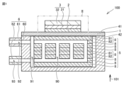
- Embodiment 1 ⁇ Configuration of the cooler> First, the configuration of a cooler 100 according to the first embodiment will be described with reference to Fig. 1 and Fig. 2. As shown in Fig. 1, the cooler 100 mainly includes a base portion 1, a joining portion 2, a joined portion 3, fins 5, and a jacket 6. The cooler 100 is a type of heat exchanger.
- the base portion 1 has, for example, a flat plate shape.
- the base portion 1 has a first surface 41 and a second surface 42.
- the first surface 41 has, for example, a planar shape.
- the second surface 42 is provided on the opposite side of the first surface 41. The direction from the second surface 42 toward the first surface 41 is defined as the first direction 101.
- the base portion 1 contains aluminum (Al).
- the material constituting the base portion 1 may be aluminum or an aluminum alloy containing aluminum as a main component. Specifically, the material constituting the base portion 1 may be pure aluminum, a 1000 series aluminum alloy, or a 3000 series aluminum alloy.
- the 1000 series aluminum alloy and the 3000 series aluminum alloy are materials specified in JIS (Japanese Industrial Standards) H4000:2014.
- the weight content of aluminum in the base portion 1 may be, for example, 90% or more, 95% or more, 99% or more, or 99.9% or more.
- the weight content of material in a member is the value obtained by dividing the weight of the material by the weight of the member.
- the joint 2 is joined to the base portion 1. Specifically, the joint 2 is joined to the base portion 1 at the first surface 41. The joint 2 is provided in the first direction 101 relative to the base portion 1.
- the joint 2 contains aluminum and silicon (Si).
- the joint 2 is made of, for example, aluminum, silicon, and unavoidable impurities.
- the joint 2 is made of, for example, an Al-Si aluminum alloy.
- the weight content of silicon in the joint 2 is, for example, 4% or more and 12% or less. It is desirable that the weight content of silicon in the joint 2 is 6% or more and 9% or less.
- the weight content of aluminum in the joint 2 may be less than the weight content of aluminum in the base portion 1.
- the joined portion 3 is provided above the joining portion 2. From another perspective, the joining portion 2 is provided between the base portion 1 and the joined portion 3.
- the joined portion 3 has a first layer 31 and a second layer 32.
- the first layer 31 is provided above the joint 2.
- the first layer 31 contains nickel.
- the first layer 31 may be made of pure nickel. Specifically, the weight content of nickel in the first layer 31 may be, for example, 99% or more.
- the first layer 31 may contain at least one of the elements contained in the joint 2 and at least one of the elements contained in the second layer 32 described below. Specifically, the first layer 31 may contain, for example, at least one of aluminum and silicon.
- the first layer 31 may contain copper (Cu).
- the second layer 32 is provided on the first layer 31.
- “provided on” includes cases where two objects are in direct contact with each other, and cases where another object is provided between the two objects so as to be in contact with each of the two objects, and the two objects are separated by the other object.
- the second layer 32 is in contact with the first layer 31.
- the second layer 32 is bonded to the first layer 31. Specifically, the second layer 32 is bonded to the first layer 31, for example, by rolling. From another perspective, the bonded portion 3 is, for example, a clad material. The second layer 32 is provided in the first direction 101 relative to the first layer 31. The second layer 32 is a portion to which other components, such as a semiconductor chip 9 (see FIG. 3), described below, are bonded, for example, by soldering.
- a semiconductor chip 9 see FIG. 3
- the second layer 32 contains copper.
- the second layer 32 may be made of pure copper. Specifically, the weight content of copper in the second layer 32 may be, for example, 99% or more.
- the second layer 32 may contain at least one of the elements contained in the first layer 31. Specifically, the second layer 32 may contain, for example, nickel.
- the cooler 100 has a compound portion 4.
- the compound portion 4 is connected to each of the joining portion 2 and the joined portion 3. Specifically, the compound portion 4 is connected to the first layer 31.
- the compound portion 4 is provided in the first direction 101 relative to the joining portion 2.
- the compound portion 4 contains at least one of the elements contained in the joint portion 2 and at least one of the elements contained in the first layer 31.
- the compound portion 4 contains, for example, aluminum and nickel (Ni).
- the compound portion 4 is composed of, for example, an Al-Ni intermetallic compound.
- the compound portion 4 may contain silicon. From another perspective, the compound portion 4 may contain a compound of silicon and nickel.
- the thickness of the joint portion 2 and the compound portion 4 in the first direction 101 is a first thickness H1.
- the first thickness H1 is, for example, 0.1 mm or less.
- the portion to be joined 3 is provided in the first direction 101 relative to the compound portion 4. From another perspective, the compound portion 4 is provided between the joining portion 2 and the portion to be joined 3. The portion to be joined 3 is separated from the joining portion 2 by the compound portion 4. In other words, the portion to be joined 3 is spaced apart from the joining portion 2. The compound portion 4 and the joining portion 2 join the portion to be joined 3 and the base portion 1.
- the first layer 31 has a third surface 43. At the third surface 43, the first layer 31 is connected to the compound portion 4. From another perspective, the third surface 43 is an interface between the first layer 31 and the compound portion 4. The first layer 31 is provided between the second layer 32 and the compound portion 4. The thickness of the first layer 31 in the first direction 101 is a seventh thickness H7.
- the second layer 32 has a fifth surface 45, a sixth surface 46, a first side surface 21, and a second side surface 22. At the fifth surface 45, the second layer 32 is joined to the first layer 31. From another perspective, the fifth surface 45 is the interface between the second layer 32 and the first layer 31.
- the thickness of the second layer 32 in the first direction 101 is the eighth thickness H8.
- the eighth thickness H8 is at least twice the seventh thickness H7.
- the sixth surface 46 is provided on the opposite side of the fifth surface 45.
- the sixth surface 46 is, for example, planar.
- the sixth surface 46 is a surface to which other components such as a semiconductor chip 9 (see FIG. 3) described below are soldered.
- the first side surface 21 is connected to both the fifth surface 45 and the sixth surface 46.
- the first side surface 21 is spaced apart from the first layer 31.
- the second side surface 22 is provided on the opposite side of the first side surface 21.
- the second side surface 22 is connected to both the fifth surface 45 and the sixth surface 46.
- the second side surface 22 is spaced apart from the first layer 31.
- the thickness of the joined portion 3 in the first direction 101 is set to a second thickness H2.
- the second thickness H2 is, for example, 300 ⁇ m or less.
- the base portion 1, the joining portion 2, the compound portion 4, and the joined portion 3 constitute a joined structure 10.
- FIG. 2 shows the configuration of the joined structure 10 according to the first embodiment.
- the fins 5 are joined to the base portion 1. Specifically, the fins 5 are joined to the base portion 1 at the second surface 42. The fins 5 are provided on the opposite side of the base portion 1 to the joined portion 3. The fins 5 are configured to cool other components joined to the second layer 32 by transferring heat to a coolant (not shown) and dissipating the heat.
- a flow path 90 is provided in the fins 5. The flow path 90 is the portion through which the coolant flows.
- the fin 5 has a plurality of plate portions 8.
- the fin 5 is formed by stacking a plurality of plate portions 8 along the first direction 101. Two adjacent plate portions 8 are bonded to each other.
- the plate portion 8 has a bonded layer 82 and a bonding layer 81.
- the bonded layer 82 is formed, for example, of an aluminum alloy containing aluminum as a main component.
- the bonded layer 82 is formed, for example, of a 3000 series aluminum alloy.
- the bonding layer 81 is provided in the first direction 101 relative to the bonded layer 82.
- the bonding layer 81 bonds two adjacent plate portions 8.
- the bonding layer 81 in contact with the base portion 1 bonds the base portion 1 and the fins 5.
- the bonding layer 81 contains aluminum and silicon.
- the bonding layer 81 is made of, for example, an Al-Si aluminum alloy.
- the jacket 6 is joined to the base portion 1.
- the jacket 6 surrounds the fins 5.
- the jacket 6 is, for example, spaced apart from the fins 5.
- the jacket 6 and the base portion 1 form a space 91.
- the space 91 is provided between the jacket 6 and the fins 5.
- the space 91 is connected to the flow path 90.
- the jacket 6 has a main body 60, a first pipe 61, and a second pipe 62.
- the main body 60 is joined to the base 1.
- the main body 60 surrounds the fins 5.
- the main body 60 has a cylindrical shape.
- the material constituting the main body 60 may be, for example, pure aluminum, or an aluminum alloy containing aluminum as the main component.
- the first pipe 61 is attached to the main body 60.
- An inlet passage 92 is provided in the first pipe 61.
- the inlet passage 92 is connected to the space 91.
- the inlet passage 92 is a flow path through which the refrigerant that flows into the flow path 90 flows.
- the second pipe 62 is attached to the main body 60.
- An outflow passage 93 is provided in the second pipe 62.
- the outflow passage 93 is connected to the space 91.
- the outflow passage 93 is a flow path through which the refrigerant flowing out from the flow path 90 flows.
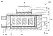
- the semiconductor device 200 has a cooler 100 and a semiconductor chip 9.
- the configuration of the cooler 100 shown in FIG. 3 is substantially the same as the configuration of the cooler 100 shown in FIG. 1.
- the semiconductor chip 9 is bonded to the second layer 32.
- the semiconductor chip 9 is bonded to the second layer 32 at the sixth surface 46 by using, for example, solder (not shown).
- the semiconductor device 200 has a chip bonding layer (not shown) that bonds the semiconductor chip 9 and the second layer 32.
- the semiconductor chip 9 may be bonded to the second layer 32 by sintering silver (not shown) or copper (not shown) arranged between the semiconductor chip 9 and the second layer 32.
- the joining method is used, for example, in joining the joined portion 3 and the base portion 1 in the manufacture of the cooler 100 shown in Fig. 1. From another perspective, the joining method is a manufacturing method of the joined structure 10 (see Fig. 2). Note that the joining method may be used for a method other than the manufacture of the cooler 100.
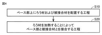
- the joining method according to the first embodiment mainly includes a step (S10) of placing the brazing material and the materials to be joined on the base portion, and a step (S20) of joining the base portion and the materials to be joined by heating the brazing material.
- a step (S10) is carried out in which the brazing material and the material to be joined are placed on the base portion.
- the base portion 1 is prepared.
- the base portion 1 has, for example, a flat plate shape.
- the base portion 1 has a first surface 41 and a second surface 42.
- the first surface 41 has, for example, a planar shape.
- the second surface 42 is provided on the opposite side of the first surface 41. The direction from the second surface 42 toward the first surface 41 is the first direction 101.
- the base portion 1 contains aluminum.
- the material constituting the base portion 1 may be aluminum or an aluminum alloy containing aluminum as a main component. Specifically, the material constituting the base portion 1 may be pure aluminum, a 1000 series aluminum alloy, or a 3000 series aluminum alloy.
- the weight content of aluminum in the base portion 1 may be, for example, 95% or more, 99% or more, or 99.9% or more.
- the flux is not particularly limited, but a non-corrosive flux such as an Al-K (potassium)-F (fluorine)-based flux or an Al-Cs (cesium)-F-based flux is preferable.
- the flux is, for example, in a paste form.
- the brazing material 12 is placed on the base portion 1. Specifically, the brazing material 12 is placed on the portion of the first surface 41 to which the flux has been supplied. From another perspective, the flux is located between the base portion 1 and the brazing material 12. The brazing material 12 is placed in the first direction 101 relative to the base portion 1.
- the brazing material 12 contains aluminum and silicon.
- the brazing material 12 is composed of, for example, aluminum, silicon, and unavoidable impurities.
- the brazing material 12 is composed of, for example, an Al-Si aluminum alloy.
- the weight content of silicon in the brazing material 12 is, for example, 4% or more and 12% or less. It is desirable that the weight content of silicon in the brazing material 12 is 6% or more and 9% or less.
- the thickness of the brazing material 12 in the first direction 101 is a third thickness H3. It is desirable that the third thickness H3 be 0.01 mm or more and 0.1 mm or less.
- the shape of the brazing material 12 is, for example, a foil shape.
- the material to be joined 13 is placed on the portion of the brazing material 12 to which the flux has been supplied.
- the flux is located between the brazing material 12 and the material to be joined 13.
- the material to be joined 13 is placed in the first direction 101 relative to the brazing material 12.
- the thickness of the material to be joined 13 in the first direction 101 is set to a fourth thickness H4. It is desirable that the fourth thickness H4 be greater than or equal to 20 ⁇ m and less than or equal to 300 ⁇ m.
- the material to be joined 13 has a first layer 31 and a second layer 32.
- the first layer 31 contacts the flux supplied onto the brazing material 12.
- the first layer 31 is located on the brazing material 12. From another perspective, the brazing material 12 is disposed between the base portion 1 and the first layer 31.
- the flux is located between the brazing material 12 and the first layer 31.
- the first layer 31 contains nickel.
- the first layer 31 is made of, for example, pure nickel.
- the weight content of nickel in the first layer 31 is, for example, 99% or more.
- the thickness of the first layer 31 in the first direction 101 is set to a fifth thickness H5. It is desirable that the fifth thickness H5 be 10 ⁇ m or more.
- the second layer 32 is provided on the first layer 31.
- the first layer 31 and the second layer 32 are joined by, for example, rolling. From another perspective, the material to be joined 13 is a clad material.
- the second layer 32 is the portion to which other members such as a semiconductor chip 9 (see FIG. 3) are joined.
- the second layer 32 contains copper.
- the second layer 32 is made of, for example, pure copper.
- the weight content of copper in the second layer 32 is 99.9% or more.
- the thickness of the second layer 32 in the first direction 101 is set to a sixth thickness H6. It is desirable that the sixth thickness H6 be 10 ⁇ m or more.
- the sixth thickness H6 is, for example, twice or more the fifth thickness H5. In this way, the brazing material 12 and the material to be joined 13 are arranged on the base portion 1.
- pressure may be applied to the base portion 1, the brazing material 12, and the material to be joined 13 in a direction parallel to the first direction 101, for example using a jig (not shown).
- the magnitude of the pressure is, for example, 10 kPa or more. This causes the flux between the base portion 1 and the brazing material 12 to be pushed out, resulting in closer adhesion between the base portion 1 and the brazing material 12.
- the flux between the brazing material 12 and the material to be joined 13 is pushed out, resulting in closer adhesion between the brazing material 12 and the material to be joined 13.
- a step (S20) is carried out in which the base portion and the workpiece are joined by heating the brazing material.
- the base portion 1, the brazing material 12, and the workpiece 13 are first placed inside a furnace (not shown).
- the inside of the furnace is an inert gas atmosphere.
- the inside of the furnace is, for example, a nitrogen atmosphere or an argon atmosphere. It is desirable that the oxygen concentration inside the furnace is 500 ppm or less. This makes it possible to prevent the brazing material 12 from oxidizing when it is heated.
- the inside of the furnace is not depressurized. Therefore, the time required to join the base portion 1 and the workpiece 13 is shortened compared to when the inside of the furnace is depressurized.
- the base portion 1, brazing material 12, and material to be joined 13 are heated inside the furnace.
- the temperature inside the furnace is equal to or higher than the melting point of the brazing material 12 and lower than the melting point of the base portion 1.
- the temperature to which the brazing material 12 is heated is equal to or higher than the melting point of the brazing material 12 and lower than the melting point of the base portion 1.
- the "melting point" of the alloy material is the solidus temperature.
- the temperature to which the brazing material 12 is heated is preferably, for example, 640°C or lower. This can prevent the base portion 1 from melting.
- the temperature to which the brazing material 12 is heated is preferably equal to or higher than the solidus temperature of the brazing material 12 and equal to or lower than the liquidus temperature of the brazing material 12. This can prevent the fluidity of the brazing material 12 from becoming excessively high. As a result, it can prevent the brazing material 12 from flowing out from between the base portion 1 and the material to be joined 13.
- the brazing material 12 melts. Specifically, when the base portion 1, the brazing material 12, and the workpiece 13 are heated, the brazing material 12 goes into a state in which, for example, a solid phase and a liquid phase coexist. The nickel contained in the first layer 31 diffuses into the molten brazing material 12.
- the base portion 1, brazing material 12, and materials to be joined 13 are cooled.
- the molten brazing material 12 solidifies. This joins the base portion 1 and materials to be joined 13.
- the joined structure 10 shown in FIG. 2 is manufactured. As shown in FIG. 2 and FIG. 5, a part of the brazing material 12 becomes the joining portion 2.
- the remaining part of the brazing material 12 becomes the compound portion 4.
- the part of the brazing material 12 into which the nickel contained in the first layer 31 has diffused becomes the compound portion 4. In this way, the base portion 1 and materials to be joined 13 are joined.
- the joining part 2 is made up of the brazing material 12.
- the compound part 4 is made up of the brazing material 12 and the first layer 31.
- a manufacturing method of the cooler 100 according to the first embodiment uses the joining method according to the first embodiment described above.
- the manufacturing method of the cooler 100 according to the first embodiment differs from the joining method according to the first embodiment mainly in that the fins 5 and the jacket 6 are joined to the base portion 1.
- the following description will focus on the differences from the configuration of the joining method according to the first embodiment.
- the manufacturing method of the cooler 100 mainly includes a step (S10) of placing the solder material and the material to be joined on the base portion, a step (S20) of joining the base portion and the material to be joined by heating the solder material, and a step (S30) of joining the jacket to the base portion.
- the fin member 15 is placed on the side of the base portion 1 opposite the material to be joined 13.
- the fin member 15 contacts the base portion 1 at the second surface 42. Flux may or may not be supplied between the fin member 15 and the base portion 1.
- the fin member 15 has a plurality of plate materials 18.
- a flow path 90 is provided in the fin member 15.
- the fin member 15 is formed by stacking a plurality of plate materials 18 along a first direction 101. Flux may or may not be supplied between two adjacent plate materials 18.
- Each of the plurality of plate materials 18 has a joining layer 82 and a brazing material layer 86.
- the bonded layer 82 is made of, for example, an aluminum alloy containing aluminum as a main component.
- the bonded layer 82 is made of, for example, a 3000-series aluminum alloy.
- the brazing material layer 86 contains aluminum and silicon.
- the brazing material layer 86 is made of, for example, an Al-Si-based aluminum alloy.
- the brazing material layer 86 is bonded to the bonded layer 82. Specifically, the brazing material layer 86 is bonded to the bonded layer 82 by, for example, rolling. From another perspective, the plate material 18 is a clad material.
- holes 98 are provided in the multiple plate materials 18.
- the holes 98 provided in the multiple plate materials 18 are connected together to form a flow path 90 (see FIG. 7).
- the minimum width of the hole 98 is, for example, about 0.2 mm.
- a pressure may be applied to the base portion 1, the brazing material 12, the workpiece 13, and the fin member 15 in a direction parallel to the first direction 101, for example using a jig (not shown).
- the magnitude of the pressure is, for example, 10 kPa or more. This causes the two adjacent plate materials 18 to adhere to each other. The base portion 1 and the fin member 15 to adhere to each other.
- the base portion 1, brazing material 12, workpiece 13, and fin member 15 are placed inside a furnace (not shown). Inside the furnace, the base portion 1, brazing material 12, workpiece 13, and fin member 15 are heated. This heats the brazing material 12 as well as the fin member 15.
- the brazing material layer 86 of the fin member 15 melts. Specifically, by heating the base portion 1, brazing material 12, workpiece 13, and fin member 15, the brazing material 12 enters a state in which, for example, a solid phase and a liquid phase coexist.
- the base portion 1, brazing material 12, material to be joined 13, and fin member 15 are cooled.
- the molten brazing material layer 86 solidifies. This bonds the fin member 15 to the base portion 1.
- Two adjacent layers to be joined 82 are bonded to each other.
- the brazing material layer 86 becomes the joining layer 81 (see Figure 1).
- the fin member 15 becomes the fin 5 (see Figure 1). In this manner, the fin member 15 is bonded to the base portion 1 by heating the brazing material 12 and the fin member 15.
- the fin 5 is composed of a fin member 15.
- the joining layer 81 is composed of a brazing material layer 86.
- the jacket 6 is disposed on the opposite side of the base portion 1 from the joined portion 3.
- the jacket 6 has a main body portion 60, a first pipe 61, and a second pipe 62.
- the main body portion 60 is joined to the base portion 1.
- the main body portion 60 surrounds the fins 5.
- the main body portion 60 has a cylindrical shape.
- the main body portion 60 may be made of, for example, pure aluminum, or an aluminum alloy containing aluminum as the main component.
- the jacket 6 is joined to the base portion 1 at the second surface 42 using a fastening method such as mechanical fastening, welding, brazing, or solid-state bonding.
- a fastening method such as mechanical fastening, welding, brazing, or solid-state bonding.
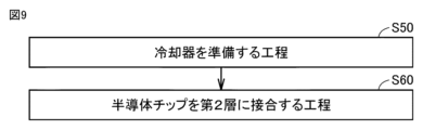
- the method for manufacturing the semiconductor device 200 according to the first embodiment includes a step (S50) of preparing a cooler and a step (S60) of bonding a semiconductor chip to the second layer.
- the step (S50) of preparing a cooler is performed.
- the cooler 100 (see FIG. 1) is prepared using the method for manufacturing the cooler 100 described above.
- a step (S60) of bonding the semiconductor chip to the second layer is performed.
- the semiconductor chip 9 is bonded to the second layer 32 at the sixth surface 46 using, for example, solder.
- a chip bonding layer 94 (see FIG. 29) is formed between the semiconductor chip 9 and the second layer 32.
- the semiconductor device 200 (see FIG. 3) is manufactured.
- the semiconductor chip 9 may be bonded to the second layer 32 by sintering silver or copper disposed between the semiconductor chip 9 and the second layer 32.
- cooler 100 The effects of the cooler 100, semiconductor device 200, bonding method, manufacturing method for the cooler 100, and manufacturing method for the semiconductor device 200 according to the first embodiment are described below.
- Aluminum-containing components are prone to the formation of dense oxide films. As a result, aluminum-containing components have poor solder wettability.
- nickel is sometimes joined to the aluminum-containing components.
- nickel can have poor solder wettability. Specifically, the solder wettability of nickel can be poor depending on the solder composition and the atmosphere inside the furnace when soldering.
- the brazing material 12 and the material to be joined 13 are placed on the base portion 1.
- the base portion 1 and the material to be joined 13 are joined.
- the base portion 1 contains aluminum.
- the material to be joined 13 has a second layer 32.
- the second layer 32 contains copper. Copper has a wide range of soldering conditions under which it has good solder wettability. Therefore, in a member (aluminum-containing member) constituted by the base portion 1, the brazing material 12, and the material to be joined 13, it is possible to provide a portion with good solder wettability. This makes it possible to improve the solder wettability of the aluminum-containing member.
- the aluminum, copper, and brazing material are typically heated to 600°C, at which point the Al-Si brazing material melts.
- a Cu-Al eutectic structure may be formed.
- the melting point of a Cu-Al eutectic structure is approximately 540°C. In other words, the melting point of this eutectic structure is lower than the heating temperature in the brazing described above. Therefore, the eutectic structure may melt during the brazing described above. As a result, the base materials of the aluminum and copper may melt and deform.
- the base portion 1 contains aluminum.
- the first layer 31 contains nickel.
- the second layer 32 contains copper.
- the second layer 32 is provided on the first layer 31.
- the brazing material 12 is placed between the base portion 1 and the first layer 31. This makes it possible to prevent the second layer 32 from coming into contact with the brazing material 12 when the brazing material 12 is heated. This makes it possible to prevent the formation of a Cu-Al eutectic structure. Therefore, the second layer 32 can be joined to the base portion 1 while suppressing melting and deformation of the base portion 1 and the second layer 32.
- the brazing material 12 is placed between the base portion 1 and the first layer 31. Therefore, when joining the base portion 1 and the material to be joined 13, the nickel contained in the first layer 31 diffuses into the brazing material 12. This forms an Al-Ni intermetallic compound. The strength of the Al-Ni intermetallic compound is high. Therefore, the base portion 1 and the material to be joined 13 can be joined more firmly.
- the weight content of silicon in the brazing material 12 is 4% or more. This allows the melting point of the brazing material 12 to be sufficiently lower than both the melting point of the base portion 1 and the melting point of the joined material 13. Therefore, when joining the base portion 1 and the joined material 13, melting of each of the base portion 1 and the joined material 13 can be suppressed.
- the brazing material 12 will be excessively hard. This will make it difficult to manufacture the brazing material 12.
- the weight content of silicon in the brazing material 12 is 12% or less. This will prevent the brazing material 12 from becoming excessively hard. As a result, it will be possible to prevent the brazing material 12 from becoming difficult to manufacture.
- the molten brazing material 12 may wet and spread onto the side surface of the workpiece 13. Therefore, the molten brazing material 12 may come into contact with the second layer 32. This may result in the formation of a Cu-Al eutectic structure.
- the weight content of silicon in the brazing material 12 may be 9% or less. This can sufficiently reduce the fluidity of the molten brazing material 12. This can more effectively prevent the molten brazing material 12 from coming into contact with the second layer 32. As a result, the formation of a Cu-Al eutectic structure can be suppressed.
- the weight content of silicon in the brazing material 12 may be 6% or more. This allows the fluidity of the brazing material 12 to be sufficiently increased. As a result, it is possible to more effectively prevent the formation of voids in the joint 2.
- the third thickness H3 of the brazing material 12 in the first direction 101 is excessively small, the volume of the molten brazing material 12 becomes excessively small when joining the base portion 1 and the joined material 13. Therefore, the molten brazing material 12 may not be used to sufficiently fill the gap between the base portion 1 and the joined material 13. This may leave a gap between the base portion 1 and the joined material 13. As a result, the reliability of the joint between the base portion 1 and the joined material 13 decreases.
- the third thickness H3 is 0.01 mm or more. Therefore, it is possible to prevent the volume of the molten brazing material 12 from becoming excessively small. This makes it possible to prevent a decrease in the reliability of the joint between the base portion 1 and the joined material 13.
- the volume of the molten brazing material 12 becomes excessively large when the base portion 1 and the material to be joined 13 are joined. Therefore, the molten brazing material 12 may flow excessively, causing wear (erosion) of the base portion 1 and the material to be joined 13, or the molten brazing material 12 may flow excessively from between the base portion 1 and the material to be joined 13. Furthermore, if the volume of the molten brazing material 12 is excessively large, nickel is excessively diffused from the first layer 31 to the brazing material 12. This causes excessive growth of Al-Ni-based intermetallic compounds. If the Al-Ni-based intermetallic compounds grow excessively, the strength of the joint between the base portion 1 and the material to be joined 13 may decrease. As a result, the reliability of the joint between the base portion 1 and the material to be joined 13 decreases.
- the third thickness H3 is 0.1 mm or less. This prevents the volume of the molten brazing material 12 from becoming excessively large. This prevents the reliability of the joining between the base portion 1 and the workpiece 13 from decreasing.
- the thickness (fourth thickness H4) of the workpiece 13 in the first direction 101 is 20 ⁇ m or more and 300 ⁇ m or less.
- the fourth thickness H4 20 ⁇ m or more it is possible to suppress melting of the workpiece 13 when the brazing material 12 is heated.
- the fourth thickness H4 300 ⁇ m or less it is possible to reduce thermal stress caused by the difference in thermal expansion coefficient between the base portion 1 and the workpiece 13.
- the thickness of the first layer 31 in the first direction 101 is 10 ⁇ m or more. This makes it possible to prevent the first layer 31 from dissolving into the brazing material 12 when the brazing material 12 is heated, thereby preventing the first layer 31 from disappearing.
- the thickness (sixth thickness H6) of the second layer 32 in the first direction 101 is 10 ⁇ m or more. This prevents nickel from appearing on the surface of the second layer 32 due to the nickel contained in the first layer 31 diffusing inside the second layer 32 when the brazing material 12 is heated.
- the fin member 15 is heated together with the brazing material 12. Therefore, by heating once, the base portion 1 and the joined portion 3 can be joined while the base portion 1 and the fin member 15 are joined. This allows the time required to manufacture the cooler 100 to be shortened.
- the cooler 100 according to the first embodiment is prepared.
- the semiconductor chip 9 is bonded to the second layer 32. Compared to aluminum, copper has good solder wettability. Therefore, the semiconductor chip 9 can be bonded more easily than when the semiconductor chip 9 is bonded to a member containing aluminum.
- the joined portion 3 is provided above the joining portion 2.
- the joined portion 3 has a first layer 31 and a second layer 32.
- the second layer 32 is provided on the first layer 31.
- the second layer 32 contains copper. Copper has a wide range of soldering conditions under which it has good solder wettability. Therefore, in the member (member containing aluminum) constituted by the base portion 1, the joining portion 2, and the joined portion 3, a portion with good solder wettability can be provided. As a result, the solder wettability of the member containing aluminum can be improved.
- the compound portion 4 is provided between the joining portion 2 and the joined portion 3.
- the compound portion 4 is connected to each of the joining portion 2 and the joined portion 3.
- the joining portion 2 contains aluminum.
- the first layer 31 contains nickel.
- the compound portion 4 contains at least one of the elements contained in the joining portion 2 and at least one of the elements contained in the first layer 31. Therefore, a compound is formed in the compound portion 4. This can increase the strength of the bond between the base portion 1 and the joined portion 3.
- the brazing material 12 is in the form of a foil, but the form of the brazing material 12 is not particularly limited.
- the brazing material 12 may be in the form of a granule or a paste.
- a solvent and a flux are mixed in the brazing material 12.
- the brazing material 12 is in the form of a paste and a flux is mixed in the brazing material 12, it is not necessary to supply a flux between the base portion 1 and the brazing material 12 and between the brazing material 12 and the joined material 13.
- the area of the brazing material 12 may be smaller than the area of the joined material 13. This prevents the volume of the molten brazing material 12 from becoming excessively large.
- the manufacturing method of the cooler 100 a configuration has been described in which the step (S30) of joining the jacket to the base portion is performed after the step (S20) of joining the base portion and the material to be joined by heating the brazing material, but the manufacturing method of the cooler 100 according to the present disclosure is not limited to the above configuration.
- the jacket 6 may be joined to the base portion 1 together with the material to be joined 13 and the fin member 15.
- the jacket 6 may be placed together with the fin member 15 on the opposite side of the material to be joined 13 with respect to the base portion 1.
- the fin member 15 may be sandwiched between the jacket 6 and the base portion 1.
- the fin member 15 and the jacket 6 may be heated together with the brazing material 12, thereby joining the fin member 15 and the jacket 6 to the base portion 1. This can shorten the time required for manufacturing the cooler 100. In the cooler 100, the fins 5 and the jacket 6 may be in contact.
- the base portion 1, the brazing material 12, the workpiece 13, the fin member 15, and the jacket 6 may each be provided with a mechanism for alignment. This can reduce the time required to position the base portion 1, the brazing material 12, the workpiece 13, the fin member 15, and the jacket 6.
- the joining method according to the second embodiment differs from the joining method according to the first embodiment mainly in that the brazing material 12 contains magnesium (Mg), and is substantially the same as the joining method according to the first embodiment in other respects.
- Mg magnesium
- the brazing material 12 may contain magnesium.
- the brazing material 12 is made of, for example, an Al-Si-Mg aluminum alloy.
- the weight content of magnesium in the brazing material 12 is, for example, 0.1% or more and 5% or less.
- the brazing material 12 contains magnesium.
- the magnesium reduces the aluminum oxide film and the nickel oxide film, thereby removing the aluminum oxide film and the nickel oxide film. Therefore, the molten brazing material 12 can easily wet and spread over the base portion 1 without supplying flux between the base portion 1 and the brazing material 12 and between the brazing material 12 and the workpiece 13. This allows the time required to join the base portion 1 and the workpiece 13 to be shortened compared to the case where flux is supplied between the base portion 1 and the brazing material 12 and between the brazing material 12 and the workpiece 13.
- the weight content of magnesium in the brazing material 12 is 0.1% or more and 5% or less. Therefore, the aluminum oxide film and the nickel oxide film can be sufficiently removed while preventing the brazing material 12 from becoming excessively hard.
- the fluidity of the molten brazing material 12 may become excessively high. In this case, the molten brazing material 12 may spread excessively, and the molten brazing material 12 may come into contact with the second layer 32.
- the base portion 1 and the material to be joined 13 can be joined without using flux. This makes it possible to prevent the fluidity of the molten brazing material 12 from becoming excessively high. This makes it possible to prevent the molten brazing material 12 from coming into contact with the second layer 32.
- the base portion 1, the brazing material 12, and the material to be joined 13 may be cleaned by pickling or the like. This makes it possible to thin the oxide films on the base portion 1, the brazing material 12, and the material to be joined 13.
- the joining method according to the third embodiment differs from the joining method according to the first embodiment mainly in that the base portion 1 contains magnesium, and is substantially the same as the joining method according to the first embodiment in other respects.
- the following description will focus on the differences from the joining method according to the first embodiment.
- the base portion 1 may contain magnesium.
- the base portion 1 is made of, for example, an Al-Si-Mg aluminum alloy.
- the base portion 1 is made of, for example, a 6000 series aluminum alloy.
- the 6000 series aluminum alloy is a material specified in JIS H4000:2014.
- the weight content of magnesium in the base portion 1 is, for example, 0.1% or more and 5% or less.
- the base portion 1 contains magnesium. Therefore, when the brazing material 12 is heated, the magnesium contained in the base portion 1 diffuses into the brazing material 12. This makes it possible to remove the oxide film of aluminum and nickel. As a result, it is possible to obtain the same effect as the joining method of the second embodiment.
- the joining method according to the fourth embodiment differs from the joining method according to the first embodiment mainly in that a groove is provided in the base portion 1, and is substantially the same as the joining method according to the first embodiment in other respects.
- the following mainly describes the differences from the joining method according to the first embodiment.
- Figure 13 shows the configuration of the base portion 1 and the workpiece 13 as viewed in the direction from the workpiece 13 toward the base portion 1.
- the first surface 41 may have a first surface portion 51 and a second surface portion 52.
- the second surface portion 52 is, for example, spaced apart from the first surface portion 51. In the first direction 101, the second surface portion 52 is provided at substantially the same position as the first surface portion 51.
- the base portion 1 may have a bottom surface 19, a first side wall surface 27, and a second side wall surface 28.
- the bottom surface 19 is provided between the first surface 41 and the second surface 42.
- the first side wall surface 27 is continuous with both the first surface portion 51 and the bottom surface 19.
- the second side wall surface 28 is continuous with both the second surface portion 52 and the bottom surface 19.
- the first side wall surface 27, the second side wall surface 28, and the bottom surface 19 form a groove 99.
- the groove 99 is provided in the base portion 1.
- the groove 99 is provided in the first surface 41.
- the groove 99 surrounds the workpiece 13 and the brazing material 12 (see FIG. 12).
- the second side wall surface 28 surrounds the workpiece 13 and the brazing material 12.
- the first side wall surface 27 surrounds the second side wall surface 28.
- the first surface portion 51 surrounds the second surface portion 52.
- the molten brazing material 12 spreads more easily on aluminum than on Ni. Therefore, in the step (S20) of joining the base portion and the workpiece by heating the brazing material, the molten brazing material 12 spreads on the surface of the base portion 1, and the molten brazing material 12 flows into the groove 99.
- a portion of the molten brazing material 12 will flow out from between the workpieces 13 and the base portion 1.
- the flowing brazing material 12 may wet and spread over the side surfaces of the workpieces 13, causing contact between the molten brazing material 12 and the second layer 32.
- a groove 99 is provided in the base portion 1. A portion of the molten brazing material 12 flows into the groove 99. Therefore, even if the molten brazing material 12 flows out from between the workpieces 13 and the base portion 1, the molten brazing material 12 can be prevented from wetting and spreading over the side surfaces of the workpieces 13. As a result, contact between the molten brazing material 12 and the second layer 32 can be prevented.
- Embodiment 5 Next, the configuration of a bonding method according to embodiment 5 will be described with reference to Figures 14 and 15.
- the bonding method according to embodiment 5 differs from the bonding method according to embodiment 1 mainly in that a part of the second layer 32 is embedded in the first layer 31, and is substantially the same as the bonding method according to embodiment 1 in other respects.
- the following description will focus on the differences from the bonding method according to embodiment 1.
- a portion of the second layer 32 may be embedded in the first layer 31.
- the material to be joined 13 is, for example, an Invar-shaped clad material.
- the first layer 31 has a seventh surface 47 and an eighth surface 48.
- the seventh surface 47 is provided on the opposite side of the third surface 43. In the first direction 101, the seventh surface 47 may be substantially in the same position as the sixth surface 46.
- the eighth surface 48 is provided on the opposite side of the third surface 43 of the second layer 32. The eighth surface 48 is spaced apart from the seventh surface 47. In the first direction 101, the seventh surface 47 may be substantially in the same position as the sixth surface 46.
- the first side surface 21 of the second layer 32 is covered by the first layer 31.
- the second side surface 22 of the second layer 32 is covered by the first layer 31.
- the second layer 32 has a third side surface 23.
- the third side surface 23 is connected to each of the sixth surface 46, the third surface 43 (see FIG. 14), the first side surface 21 (see FIG. 14), and the second side surface 22 (see FIG. 14).
- the third side surface 23 is exposed, for example, from the first layer 31. In other words, the third side surface 23 is not covered by the first layer 31.
- the direction perpendicular to the third side surface 23 is the second direction 102.
- the second direction 102 is substantially perpendicular to the first direction 101.
- the second layer 32 extends along the second direction 102.
- a part of the second layer 32 is embedded in the first layer 31. Therefore, when the molten brazing material 12 wets and spreads on the side surface of the joined material 13, the distance over which the molten brazing material 12 must wet and spread before it comes into contact with the second layer 32 can be lengthened. This makes it possible to prevent the molten brazing material 12 from coming into contact with the second layer 32.
- both ends of the workpieces 13 in the second direction 102 may be bent toward the first direction 101. From another perspective, both ends of the workpieces 13 in the second direction 102 may be bent so that the third side surface 23 is located in the first direction 101 relative to the sixth surface 46. This makes it possible to more effectively prevent the molten brazing material 12 from coming into contact with the second layer 32.
- the joining method according to the sixth embodiment differs from the joining method according to the second embodiment mainly in that the workpieces 13 and the brazing material 12 are integrally formed, and the remaining points are substantially the same as those of the joining method according to the second embodiment.
- the following description will focus on the points that differ from the joining method according to the second embodiment.
- the material to be joined 13 and the brazing material 12 may be formed integrally. From another perspective, the material to be joined 13 and the brazing material 12 may form a structure 50.
- the structure 50 is a clad material.
- the structure 50 is placed on the base portion 1, so that the brazing material 12 and the workpiece 13 are placed on the base portion 1.
- the workpiece 13 and the brazing material 12 are formed integrally. This makes it easier to arrange the brazing material 12 and the workpiece 13 in the step (S10) of arranging the brazing material and the workpiece 13 on the base portion. This makes it possible to shorten the time required to join the base portion 1 and the workpiece 13.
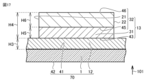
- Embodiment 7 the configuration of the joining method according to the seventh embodiment will be described with reference to Fig. 17.
- the joining method according to the seventh embodiment differs from the joining method according to the second embodiment mainly in that the base portion 1 and the brazing material 12 are integrally formed, and the remaining points are substantially the same as those of the joining method according to the second embodiment.
- the following description will focus on the points that differ from the joining method according to the second embodiment.
- the base portion 1 and the brazing material 12 may be formed as one unit. From another point of view, the base portion 1 and the brazing material 12 may form a base structure 70. The base portion 1 and the brazing material 12 are joined by, for example, rolling. The brazing material 12 covers, for example, the first surface 41.
- a base structure 70 is prepared.
- the material to be joined 13 is placed on the base structure 70.
- a part of the brazing material 12 may be removed using a processing method such as cutting.
- the base portion 1 and the brazing material 12 are formed as one unit. This makes it easier to place the brazing material 12 in the step (S10) of placing the brazing material and the material to be joined on the base portion. This makes it possible to shorten the time required to join the base portion 1 and the material to be joined 13.
- the joining method according to the eighth embodiment differs from the joining method according to the first embodiment mainly in that the workpieces 13 have a third layer, and is substantially the same as the joining method according to the first embodiment in other respects.
- the following description will focus on the differences from the joining method according to the first embodiment.
- the material to be joined 13 may have a third layer 33.
- the third layer 33 is provided on the first layer 31.
- the third layer 33 is in contact with each of the first layer 31 and the second layer 32.
- the third layer 33 is provided between the first layer 31 and the second layer 32. From another perspective, the second layer 32 is separated from the first layer 31 by the third layer 33.
- the third layer 33 may be joined to each of the first layer 31 and the second layer 32 by rolling.
- the third layer 33 contains titanium (Ti).
- the third layer 33 is made of, for example, pure titanium.
- the weight content of titanium in the third layer 33 may be, for example, 99% or more.
- the first layer 31 and the second layer 32 are also heated along with the brazing material 12. Therefore, when the first layer 31 and the second layer 32 are in contact with each other, the nickel contained in the first layer 31 diffuses into the second layer 32. Similarly, the copper contained in the second layer 32 diffuses into the first layer 31.
- the copper diffused into the first layer 31 may come into contact with the brazing material 12. This causes an Al-Cu eutectic structure to be formed.
- the melting point of the Al-Cu eutectic structure is lower than both the melting point of the brazing material 12 and the melting point of the base portion 1. This may cause the base portion 1 to melt and deform.
- the nickel diffused into the second layer 32 may appear on the surface of the second layer 32. This may cause the solderability of the second layer 32 to deteriorate.
- the material to be joined 13 has a third layer 33.
- the third layer 33 is provided between the first layer 31 and the second layer 32.
- the third layer 33 contains titanium. Therefore, the third layer 33 can suppress the diffusion of copper and nickel between the first layer 31 and the second layer 32. This can suppress the melting and deformation of the base portion 1 while suppressing the deterioration of the solderability in the second layer 32.
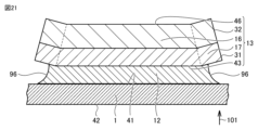
- Embodiment 9 Next, the configuration of a joining method according to embodiment 9 will be described with reference to Figures 19 to 22.
- the joining method according to embodiment 9 differs from the joining method according to embodiment 1 mainly in that the outer periphery of the workpiece 13 is bent, and is substantially the same as the joining method according to embodiment 1 in other respects.
- the following description will focus on the differences from the joining method according to embodiment 1.
- the material to be joined 13 is composed of a central portion 16 and an outer peripheral portion 17.
- the outer peripheral portion 17 surrounds the central portion 16.
- the outer peripheral portion 17 is connected to the central portion 16.
- Each of the central portion 16 and the outer peripheral portion 17 is composed of a first layer 31 and a second layer 32.
- the central portion 16 is in contact with the brazing material 12.
- the outer peripheral portion 17 is spaced apart from the brazing material 12.
- the outer peripheral portion 17 is bent in the first direction 101 relative to the central portion 16. From another perspective, the outer peripheral portion 17 is floated.
- the outer peripheral portion 17 is inclined in the first direction 101 relative to the central portion 16. The distance between the outer peripheral portion 17 and the base portion 1 in the first direction 101 increases with increasing distance from the central portion 16.
- the outer peripheral portion 17 is inclined in the first direction 101 with respect to the central portion 16.
- the molten brazing material 12 flows into the space between the outer peripheral portion 17 and the base portion 1. This forms a fillet 96 in the molten brazing material 12.
- the capillary force acting on the molten brazing material 12 is reduced. This makes it difficult for the molten brazing material 12 to flow. This makes it possible to prevent the brazing material 12 from flowing out from between the base portion 1 and the workpiece 13. This also makes it possible to prevent the molten brazing material 12 from coming into contact with the second layer 32. This makes it possible to prevent erosion of the second layer 32 caused by contact between the molten brazing material 12 and the second layer 32.
- the outer peripheral portion 17 may be formed by the part where the sagging and burrs are formed.
- the outer peripheral portion 17 may be folded back.
- the outer peripheral portion 17 may be in contact with a portion of the second layer 32 in the central portion 16.
- the portion of the second layer 32 in the outer peripheral portion 17 may be in contact with a portion of the second layer 32 in the central portion 16.
- the portion of the second layer 32 in the outer peripheral portion 17 faces the portion of the second layer 32 in the central portion 16.
- the second layer 32 is surrounded by the first layer 31.
- FIG. 22 shows the state after the step (S10) of placing the brazing material and the material to be joined on the base portion.
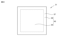
- Embodiment 10 Next, the configuration of a bonding method according to embodiment 10 will be described with reference to Figures 23 to 25.
- the bonding method according to embodiment 10 differs from the bonding method according to embodiment 1 mainly in that an anti-wetting agent is applied to the first layer 31, and is substantially the same as the bonding method according to embodiment 1 in other respects.
- the following description will focus on the differences from the bonding method according to embodiment 1.
- the joining method according to the tenth embodiment includes a step (S15) of applying an anti-wetting agent to the first layer.
- the step (S15) of applying an anti-wetting agent to the first layer is carried out, for example, after the step (S10) of placing the brazing material and the materials to be joined on the base portion and before the step (S20) of joining the base portion and the materials to be joined by heating the brazing material.
- the third surface 43 is composed of a bonding region 35 and a non-bonding region 36.
- the bonding region 35 is an area that comes into contact with the brazing material 12.
- the non-bonding region 36 is an area to which a wetting inhibitor 39, which will be described later, is applied.
- the non-bonding region 36 is continuous with the bonding region 35.
- the non-bonding region 36 surrounds the bonding region 35.
- the non-bonding region 36 is located on the outer periphery of the third surface 43.
- the first layer 31 has a first outer peripheral side surface 37.
- the first outer peripheral side surface 37 is continuous with the non-bonding region 36.
- the first outer peripheral side surface 37 is annular in shape.
- the second layer 32 has a second outer peripheral side surface 38.
- the second outer peripheral side surface 38 is annular.
- the second outer peripheral side surface 38 includes the first side surface 21 and the second side surface 22 (see FIG. 2).
- the second outer peripheral side surface 38 is continuous with each of the fifth surface 45 and the sixth surface 46.
- a wetting inhibitor 39 is applied to at least a portion of the non-bonding region 36.
- the surface of the wetting inhibitor 39 is difficult for the molten brazing material 12 to spread over. From another perspective, the wettability of the surface of the wetting inhibitor 39 to the molten brazing material 12 is lower than the wettability of the third surface 43 to the molten brazing material 12.
- the wetting inhibitor 39 inhibits the molten brazing material 12 from spreading over.
- the wetting inhibitor 39 is also called a stop-off agent.
- the wetting inhibitor 39 is composed of, for example, at least one of oxide particles and ceramics, and a binder (solvent).
- Anti-wetting agent 39 may be applied to the entire non-bonded region 36.
- the anti-wetting agent 39 may be applied to the first outer peripheral side surface 37, the second outer peripheral side surface 38, or the outer peripheral end of the sixth surface 46.
- the joining region 35 is in contact with the brazing material 12.
- the joining region 35 and the brazing material 12 are in contact without the wetting inhibitor 39.
- the brazing material 12 is surrounded by the wetting inhibitor 39.
- the non-joining region 36 is spaced apart from the brazing material 12.
- the width of the workpiece 13 is greater than the width of the brazing material 12.
- the brazing material 12 overlaps the workpiece 13.
- a wetting inhibitor 39 is applied to the non-joining region 36 of the first layer 31. Therefore, in the step (S20) of joining the base portion and the joined material by heating the brazing material, the wetting inhibitor 39 prevents the molten brazing material 12 from wetting and spreading over the surface of the first layer 31. This makes it possible to prevent the molten brazing material 12 from coming into contact with the second layer 32. Therefore, it is possible to prevent erosion of the second layer 32 caused by contact between the molten brazing material 12 and the second layer 32.
- the step (S15) of applying a wetting inhibitor to the first layer may be performed before the step (S10) of placing the brazing material and the materials to be joined on the base portion.
- the step (S15) of applying a wetting inhibitor to the first layer may be performed before the step (S20) of joining the base portion and the materials to be joined by heating the brazing material.
- Embodiment 11 Next, the configuration of the manufacturing method of the cooler according to embodiment 11 will be described with reference to Figures 26 and 27.
- the manufacturing method of the cooler according to embodiment 11 differs from the manufacturing method of the cooler according to embodiment 1 mainly in that a blasting treatment is performed on the surface of the second layer 32, and is substantially the same as the manufacturing method of the cooler according to embodiment 1 in other respects.
- the following description will focus on the differences from the manufacturing method of the cooler according to embodiment 1.
- the manufacturing method for the cooler 100 according to the eleventh embodiment includes a step (S25) of performing a blasting treatment on the surface of the second layer.
- the manufacturing method for the semiconductor device 200 according to the eleventh embodiment includes a step (S25) of performing a blasting treatment on the surface of the second layer.
- the step (S25) of blasting the surface of the second layer is carried out after the step (S20) of joining the base portion and the workpiece by heating the brazing material, for example, and before the step (S30) of joining the jacket to the base portion.
- the sixth surface 46 is blasted.
- the blasting is a process in which hard fine particles are collided with an object to process it. Specifically, fine particles 95 are projected onto the sixth surface 46. The fine particles 95 collide with the sixth surface 46, causing the sixth surface 46 to be slightly scraped. This may result in minute irregularities (not shown) being formed on the sixth surface 46.
- the blasting process may be either wet blasting or dry blasting.
- wet blasting When wet blasting is used, the number of fine particles 95 embedded in the sixth surface 46 can be reduced.
- the material constituting the fine particles 95 may be, for example, a metal such as iron, stainless steel, aluminum, or copper, or it may be ceramics, glass, or dry ice. When the fine particles 95 are composed of dry ice, it is possible to prevent the fine particles 95 from remaining on the sixth surface 46.
- the glossiness of the sixth surface 46 before the step (S25) of blasting the surface of the second layer is low.
- the step (S25) of blasting the surface of the second layer may be performed after the step (S30) of joining the jacket to the base portion.
- the blasting may be performed on the surface of the second layer 32.
- the surface of the second layer 32 is the surface of the second layer 32 that is not covered by either the first layer 31 or the third layer 33 (see FIG. 18).
- the configuration of the cooler 100 according to the eleventh embodiment will be described with reference to FIG. 28.
- the surface of the second layer 32 is blasted.
- the sixth surface 46 is blasted.
- the sixth surface 46 may have minute irregularities.
- the cooler 100 may have fine particles 95.
- the fine particles 95 are located on the sixth surface 46.
- the fine particles 95 are embedded in the second layer 32 at the sixth surface 46.
- the fine particles 95 are the fine particles 95 used in the blasting process in the step (S25) of performing the blasting process on the surface of the second layer.
- the semiconductor device 200 according to the eleventh embodiment has, for example, a particle 95.
- the particle 95 is located on the sixth surface 46.
- the particle 95 is embedded in the second layer 32 at the sixth surface 46.
- the particles 95 are located between the second layer 32 and the semiconductor chip 9. Specifically, the particles 95 are located between the second layer 32 and the chip bonding layer 94.
- the sixth surface 46 is blasted.
- the sixth surface 46 may have minute irregularities.
- Each of the first side surface 21 and the second side surface 22 may be blasted.
- the second layer 32 is heated to a high temperature. This may cause the surface of the second layer 32 to oxidize or discolor. Furthermore, in the process of manufacturing the cooler 100, the surface of the second layer 32 may be pressed down using a jig or the like. In this case, the jig may leave marks on the surface of the second layer 32, or the surface of the second layer 32 may become contaminated due to contact with the jig.
- the manufacturing method of the cooler 100 according to the eleventh embodiment includes a step (S25) of blasting the surface of the second layer 32 after a step (S20) of joining the base portion and the material to be joined by heating the brazing material. Therefore, the blasting can remove oxides and foreign matter located on the surface of the second layer 32. This can make the surface condition of the second layer 32 more uniform. This can make it easier to solder other components to the second layer 32.
- the manufacturing method of the semiconductor device 200 according to the eleventh embodiment includes a step (S25) of blasting the surface of the second layer 32 after the step (S20) of joining the base portion and the material to be joined by heating the brazing material. This makes it possible to make the surface condition of the second layer 32 more uniform, as described above. This improves the reliability of the joining between the semiconductor chip 9 and the second layer 32.
- the manufacturing method of the cooler 100 may use the joining method according to each of the above-mentioned embodiments 2 to 10.
- the compound part 4 may contain magnesium.
- the compound part 4 may contain a compound of magnesium and nickel.
- the compound part 4 may contain magnesium.
- the compound part 4 may contain a compound of magnesium and nickel.
- the brazing material contains aluminum and silicon,
- the workpiece is a first layer comprising nickel; a second layer disposed on the first layer and comprising copper;
- a joining method wherein in the step of placing the brazing material and the workpiece, the brazing material is placed between the base portion and the first layer.
- the brazing material includes aluminum, silicon, and magnesium, 2.
- the brazing material in the process of joining the base portion and the workpiece by heating the brazing material at a temperature equal to or higher than the melting point of the brazing material and lower than the melting point of the base portion, the brazing material is heated in an inert gas atmosphere.
- the base portion comprises magnesium; 2.
- the brazing material in the process of joining the base portion and the workpiece by heating the brazing material at a temperature equal to or higher than the melting point of the brazing material and lower than the melting point of the base portion, the brazing material is heated in an inert gas atmosphere.
- the second layer has a thickness that is at least twice the thickness of the first layer.
- a groove is provided in the base portion, 5.
- the workpiece is configured with a central portion and an outer peripheral portion surrounding the central portion, Prior to a step of joining the base portion and the workpiece by heating the brazing material at a temperature equal to or higher than a melting point of the brazing material and lower than a melting point of the base portion, the central portion is in contact with the brazing material;
- the joining method according to any one of claims 1 to 5, wherein the outer circumferential portion is bent relative to the central portion in a direction from the base portion toward the brazing material.
- the first layer has a third surface including a bonded region and a non-bonded region connected to the bonded region, Prior to a step of joining the base portion and the workpiece by heating the brazing material at a temperature equal to or higher than a melting point of the brazing material and lower than a melting point of the base portion, the joining region is in contact with the brazing material; The non-bonded region is spaced apart from the brazing material;
- the joining method according to any one of claims 1 to 6, further comprising a step of applying an anti-wetting agent to the non-joining region before a step of joining the base portion and the workpieces by heating the brazing material at a temperature equal to or higher than a melting point of the brazing material and lower than a melting point of the base portion.
- (Appendix 12) A method for manufacturing a cooler using the joining method according to any one of Supplementary Note 1 to Supplementary Note 11, In the step of placing the brazing material and the workpiece on the base portion, a fin member is placed on the opposite side of the workpiece with respect to the base portion; A method for manufacturing a cooler, in a process of joining the base portion and the material to be joined by heating the brazing material at a temperature equal to or higher than the melting point of the brazing material and lower than the melting point of the base portion, the fin member is joined to the base portion by heating the fin member together with the brazing material.
- the method for manufacturing a cooler described in Appendix 12 further comprises a step of blasting a surface of the second layer after a step of joining the base portion and the material to be joined by heating the brazing material at a temperature equal to or higher than the melting point of the brazing material and lower than the melting point of the base portion.
- Appendix 14 Preparing a cooler using the method for producing a cooler according to claim 12 or 13; A method for manufacturing a semiconductor device, comprising the step of bonding a semiconductor chip to the second layer of the cooler.
- (Appendix 15) a base portion including aluminum; a joint portion joined to the base portion; A joint portion provided above the joint portion; a compound portion provided between the joining portion and the joined portion and connected to each of the joining portion and the joined portion; a fin joined to the base portion and provided on the opposite side of the joined portion with respect to the base portion, the joint portion includes aluminum and silicon;
- the joined portion is a first layer connected to the compound portion and containing nickel; a second layer disposed on the first layer and comprising copper;
- a cooler wherein the compound portion contains at least one of the elements contained in the bonding portion and at least one of the elements contained in the first layer.
- (Appendix 16) 16 16. The cooler of claim 15, wherein the surface of the second layer is blasted.
Landscapes
- Engineering & Computer Science (AREA)
- Mechanical Engineering (AREA)
- Chemical & Material Sciences (AREA)
- Materials Engineering (AREA)
- Cooling Or The Like Of Semiconductors Or Solid State Devices (AREA)
Priority Applications (1)
| Application Number | Priority Date | Filing Date | Title |
|---|---|---|---|
| JP2025539352A JPWO2025033315A1 (https=) | 2023-08-07 | 2024-08-01 |
Applications Claiming Priority (2)
| Application Number | Priority Date | Filing Date | Title |
|---|---|---|---|
| JP2023128457 | 2023-08-07 | ||
| JP2023-128457 | 2023-08-07 |
Publications (1)
| Publication Number | Publication Date |
|---|---|
| WO2025033315A1 true WO2025033315A1 (ja) | 2025-02-13 |
Family
ID=94533845
Family Applications (1)
| Application Number | Title | Priority Date | Filing Date |
|---|---|---|---|
| PCT/JP2024/027519 Pending WO2025033315A1 (ja) | 2023-08-07 | 2024-08-01 | 接合方法、冷却器の製造方法、半導体装置の製造方法、冷却器および半導体装置 |
Country Status (2)
| Country | Link |
|---|---|
| JP (1) | JPWO2025033315A1 (https=) |
| WO (1) | WO2025033315A1 (https=) |
Citations (7)
| Publication number | Priority date | Publication date | Assignee | Title |
|---|---|---|---|---|
| JP2002184922A (ja) * | 2000-12-12 | 2002-06-28 | Ntt Advanced Technology Corp | 複合型放熱部材 |
| JP2002346737A (ja) * | 2001-05-22 | 2002-12-04 | Denso Corp | 異種金属のろう付け方法 |
| JP2002361408A (ja) * | 2001-06-11 | 2002-12-18 | Denso Corp | 異種金属接合品の接合方法 |
| WO2016052392A1 (ja) * | 2014-09-30 | 2016-04-07 | 三菱マテリアル株式会社 | Ag下地層付パワーモジュール用基板及びパワーモジュール |
| JP2016048782A (ja) * | 2014-08-26 | 2016-04-07 | 三菱マテリアル株式会社 | 接合体、ヒートシンク付パワーモジュール用基板、ヒートシンク、接合体の製造方法、ヒートシンク付パワーモジュール用基板の製造方法、及び、ヒートシンクの製造方法 |
| WO2021060475A1 (ja) * | 2019-09-25 | 2021-04-01 | 京セラ株式会社 | 電子部品搭載用基体および電子装置 |
| JP2023055323A (ja) * | 2021-10-06 | 2023-04-18 | 三菱電機株式会社 | 半導体装置用基板、半導体装置用基板の製造方法および接合材 |
-
2024
- 2024-08-01 WO PCT/JP2024/027519 patent/WO2025033315A1/ja active Pending
- 2024-08-01 JP JP2025539352A patent/JPWO2025033315A1/ja active Pending
Patent Citations (7)
| Publication number | Priority date | Publication date | Assignee | Title |
|---|---|---|---|---|
| JP2002184922A (ja) * | 2000-12-12 | 2002-06-28 | Ntt Advanced Technology Corp | 複合型放熱部材 |
| JP2002346737A (ja) * | 2001-05-22 | 2002-12-04 | Denso Corp | 異種金属のろう付け方法 |
| JP2002361408A (ja) * | 2001-06-11 | 2002-12-18 | Denso Corp | 異種金属接合品の接合方法 |
| JP2016048782A (ja) * | 2014-08-26 | 2016-04-07 | 三菱マテリアル株式会社 | 接合体、ヒートシンク付パワーモジュール用基板、ヒートシンク、接合体の製造方法、ヒートシンク付パワーモジュール用基板の製造方法、及び、ヒートシンクの製造方法 |
| WO2016052392A1 (ja) * | 2014-09-30 | 2016-04-07 | 三菱マテリアル株式会社 | Ag下地層付パワーモジュール用基板及びパワーモジュール |
| WO2021060475A1 (ja) * | 2019-09-25 | 2021-04-01 | 京セラ株式会社 | 電子部品搭載用基体および電子装置 |
| JP2023055323A (ja) * | 2021-10-06 | 2023-04-18 | 三菱電機株式会社 | 半導体装置用基板、半導体装置用基板の製造方法および接合材 |
Also Published As
| Publication number | Publication date |
|---|---|
| JPWO2025033315A1 (https=) | 2025-02-13 |
Similar Documents
| Publication | Publication Date | Title |
|---|---|---|
| CN108602317B (zh) | 铝多层钎焊板制品和无钎剂钎焊方法 | |
| CN100581700C (zh) | 用于硬钎焊的铝合金带 | |
| JP6483412B2 (ja) | 熱交換器用アルミニウム合金クラッド材 | |
| JP6186455B2 (ja) | 熱交換器及びその製造方法 | |
| CN101715380A (zh) | 铝合金硬钎焊板材 | |
| JP4698416B2 (ja) | ドロンカップ型熱交換器の製造方法、アルミニウムクラッド板材およびドロンカップ型熱交換器 | |
| KR20190098256A (ko) | 플럭스-프리 cab 브레이징용 알루미늄 재료 | |
| JP6474589B2 (ja) | 熱交換器用アルミニウム合金クラッド材 | |
| WO2017208940A1 (ja) | ブレージングシート及びその製造方法並びにアルミニウム構造体のろう付方法 | |
| JP5713451B2 (ja) | アルミニウム合金ブレージングシートとその製造方法、およびアルミニウム製熱交換器のろう付け方法 | |
| JP5853727B2 (ja) | ヒートシンク付パワーモジュール用基板の製造方法 | |
| JP5490603B2 (ja) | アルミニウム部材のろう付方法 | |
| WO2025033315A1 (ja) | 接合方法、冷却器の製造方法、半導体装置の製造方法、冷却器および半導体装置 | |
| JP4350753B2 (ja) | ヒートシンク部材およびその製造方法 | |
| TWI465308B (zh) | Aluminum alloy welding method | |
| JP7164498B2 (ja) | アルミニウム合金材、フラックスレスろう付構造体、および、フラックスレスろう付方法 | |
| JP6426883B2 (ja) | 耐食性に優れた接合体の製造方法 | |
| JP7796503B2 (ja) | 半導体装置用基板、半導体装置用基板の製造方法および接合材 | |
| JP2004156108A (ja) | ろう付け用アルミニウムクラッド材 | |
| JP2013197185A (ja) | ヒートシンク付パワーモジュール用基板の製造方法およびパワーモジュール用基板 | |
| JP6033542B2 (ja) | 接合体及びその製造方法 | |
| WO2024143290A1 (ja) | アルミニウム材の接合方法、熱交換器の製造方法、加圧装置、ろう付接合体、及び、熱交換器 | |
| WO2024241673A1 (ja) | 接合方法、半導体装置の製造方法及び半導体装置 | |
| JP6745578B2 (ja) | 面接合用ろう材シート | |
| JP2006341304A (ja) | 異種金属接合法 |
Legal Events
| Date | Code | Title | Description |
|---|---|---|---|
| 121 | Ep: the epo has been informed by wipo that ep was designated in this application |
Ref document number: 24851740 Country of ref document: EP Kind code of ref document: A1 |
|
| ENP | Entry into the national phase |
Ref document number: 2025539352 Country of ref document: JP Kind code of ref document: A |
|
| WWE | Wipo information: entry into national phase |
Ref document number: 2025539352 Country of ref document: JP |
|
| NENP | Non-entry into the national phase |
Ref country code: DE |