WO2025033292A1 - 電気コネクタ付ケーブル - Google Patents
電気コネクタ付ケーブル Download PDFInfo
- Publication number
- WO2025033292A1 WO2025033292A1 PCT/JP2024/027395 JP2024027395W WO2025033292A1 WO 2025033292 A1 WO2025033292 A1 WO 2025033292A1 JP 2024027395 W JP2024027395 W JP 2024027395W WO 2025033292 A1 WO2025033292 A1 WO 2025033292A1
- Authority
- WO
- WIPO (PCT)
- Prior art keywords
- cable
- ferrule
- tip
- tip region
- coating
- Prior art date
- Legal status (The legal status is an assumption and is not a legal conclusion. Google has not performed a legal analysis and makes no representation as to the accuracy of the status listed.)
- Pending
Links
Images


Classifications
-
- H—ELECTRICITY
- H01—ELECTRIC ELEMENTS
- H01R—ELECTRICALLY-CONDUCTIVE CONNECTIONS; STRUCTURAL ASSOCIATIONS OF A PLURALITY OF MUTUALLY-INSULATED ELECTRICAL CONNECTING ELEMENTS; COUPLING DEVICES; CURRENT COLLECTORS
- H01R12/00—Structural associations of a plurality of mutually-insulated electrical connecting elements, specially adapted for printed circuits, e.g. printed circuit boards [PCB], flat or ribbon cables, or like generally planar structures, e.g. terminal strips, terminal blocks; Coupling devices specially adapted for printed circuits, flat or ribbon cables, or like generally planar structures; Terminals specially adapted for contact with, or insertion into, printed circuits, flat or ribbon cables, or like generally planar structures
- H01R12/50—Fixed connections
- H01R12/59—Fixed connections for flexible printed circuits, flat or ribbon cables or like structures
-
- H—ELECTRICITY
- H01—ELECTRIC ELEMENTS
- H01R—ELECTRICALLY-CONDUCTIVE CONNECTIONS; STRUCTURAL ASSOCIATIONS OF A PLURALITY OF MUTUALLY-INSULATED ELECTRICAL CONNECTING ELEMENTS; COUPLING DEVICES; CURRENT COLLECTORS
- H01R13/00—Details of coupling devices of the kinds covered by groups H01R12/70 or H01R24/00 - H01R33/00
- H01R13/646—Details of coupling devices of the kinds covered by groups H01R12/70 or H01R24/00 - H01R33/00 specially adapted for high-frequency, e.g. structures providing an impedance match or phase match
- H01R13/6473—Impedance matching
Definitions
- the present disclosure relates to cables with electrical connectors.
- This application claims priority based on Japanese Application No. 2023-131312 filed on August 10, 2023, and incorporates by reference all of the contents of said Japanese application.
- Patent document 1 discloses an example of a cable having multiple conductors and a coating. In this cable, a portion of the conductor is exposed from the coating. A conductor is electrically connected to the approximate center of the exposed portion.
- the cable with electrical connector of the present disclosure comprises at least one cable having multiple conductors and a coating covering the multiple conductors, and a ferrule that surrounds and holds the tip region of the cable.
- the outer surface of each of the multiple conductors in the tip region is covered by the coating and is not exposed from the coating.
- the tip surface of each of the multiple conductors in the tip region is exposed from the coating and the ferrule.
- FIG. 1 is a front view of an electric connector-attached cable according to a first embodiment.
- FIG. 2 is a cross-sectional view of the cable with electrical connector shown in FIG.
- FIG. 3 is a cross-sectional view of the flat cable shown in FIG.
- FIG. 4 is a cross-sectional view of the flat cable shown in FIG.
- FIG. 5 is a cross-sectional view of the cable with electric connector according to the second embodiment.
- FIG. 6 is a cross-sectional view of the cable with electric connector taken along line VI-VI shown in FIG.
- FIG. 7 is a cross-sectional view of an electric connector cable according to a first modified example.
- FIG. 8 is a front view of an electric connector cable according to a second modified example.
- FIG. 9 is a cross-sectional view of the cable with electrical connector shown in FIG.
- FIG. 10 is a cross-sectional view of a cable with an electric connector according to a modified example.
- the cable with electrical connector of the present disclosure comprises at least one cable having multiple conductors and a coating covering the multiple conductors, and a ferrule surrounding a tip region of the cable and holding the tip region.
- the outer surfaces of each of the multiple conductors in the tip region are covered by the coating and are not exposed from the coating.
- the tip surfaces of each of the multiple conductors in the tip region are exposed from the coating and the ferrule.
- the outer surface of each of the multiple conductors in the tip region is covered by the coating and is not exposed from the coating. This reduces the unevenness of the dielectric constant distribution around the conductor, for example, compared to when the outer surface of the conductor in the tip region is exposed from the coating. Meanwhile, the tip surface of each of the multiple conductors in the tip region is exposed from the coating and the ferrule.
- this cable with electrical connector can prevent a decrease in communication performance.
- the cable with electrical connector of the present disclosure comprises at least one cable having a plurality of conductors and a coating covering the plurality of conductors, a ferrule surrounding a tip region of the cable and holding the tip region, and a dielectric constant adjustment sheet provided between the tip region and the ferrule.
- the outer surfaces of each of the plurality of conductors in the tip region are covered by the dielectric constant adjustment sheet while being exposed from the coating.
- the tip surfaces of each of the plurality of conductors in the tip region are exposed from the dielectric constant adjustment sheet and the ferrule.
- the outer surface of each of the multiple conductors in the tip region is covered with a dielectric constant adjustment sheet while exposed from the coating. This reduces the unevenness of the dielectric constant distribution around the conductor, for example, compared to when the outer surface of the conductor in the tip region is exposed. Meanwhile, the tip surface of each of the multiple conductors in the tip region is exposed from the dielectric constant adjustment sheet and the ferrule.
- this cable with electrical connector can prevent a decrease in communication performance.
- the ferrule may have a plurality of holding members.
- the tip region of the cable may be sandwiched between the plurality of holding members while being disposed between the plurality of holding members. In this case, the tip region of the cable is securely held by the first holding member and the second holding member.
- the at least one cable may include a plurality of cables.
- the plurality of cables may be arranged in parallel. In this case, the tip regions of each of the plurality of cables are securely held.
- the tip region of the cable may be bent inside the ferrule. In this case, the degree of freedom in the arrangement of the cable with electrical connector is improved.
- the tip region of the cable may be bent inside the ferrule, and the boundary between the coating and the dielectric constant adjustment sheet may be provided at a position where the conductor extends in a straight line toward the tip surface.
- the conductor and the dielectric constant adjustment sheet are bonded together flatly by the ferrule, making it easier to match impedance.
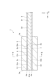
- FIG. 1 is a front view of the cable with an electrical connector of the first embodiment.
- FIG. 2 is a cross-sectional view of the cable with an electrical connector taken along line II-II shown in FIG. 1.
- the cable with an electrical connector 1 includes a flat cable 2 and a ferrule 3.
- the flat cable 2 is, for example, a flexible flat cable (FFC).
- the flat cable 2 has a plurality of conductors 21 and a coating 22.
- Each conductor 21 has a cross section perpendicular to the length direction that is, for example, a circle or an ellipse.
- Each conductor 21 extends along the Y-axis direction.
- the plurality of conductors 21 are lined up along the X-axis direction.
- Each conductor 21 has, for example, a circular shape in a cross section along the XZ plane.
- the material of the conductors 21 is, for example, copper.
- the conductors 21 function, for example, as an operating electrode. At least one of the plurality of conductors 21 may function, for example, as a ground electrode.
- the coating 22 covers the plurality of conductors 21.
- the coating 22 bundles the plurality of conductors 21.
- the ferrule 3 surrounds the tip region 2a of the flat cable 2.
- the ferrule 3 includes a tip face 3a, a rear end face 3b, and an insertion hole 3c.
- the tip face 3a and the rear end face 3b are flat faces that intersect or are perpendicular to the Y-axis direction.
- the rear end face 3b faces the opposite side to the tip face 3a.
- the insertion hole 3c penetrates the ferrule 3 in the Y-axis direction.
- the insertion hole 3c opens on each of the tip face 3a and the rear end face 3b.
- the tip region 2a of the flat cable 2 is inserted into the insertion hole 3c.
- the region of the flat cable 2 that is inserted into the insertion hole 3c is the tip region 2a.
- the region of the flat cable 2 that is located between the tip face 3a and the rear end face 3b of the ferrule 3 is the tip region 2a.
- the outer peripheral surface 21c (outer surface) of each conductor 21 in the tip region 2a of the flat cable 2 is covered with the coating 22. That is, the area of the outer peripheral surface 21c of each conductor 21 located inside the insertion hole 3c of the ferrule 3 is covered with the coating 22. In this embodiment, the entire area of the outer peripheral surface 21c of each conductor 21 is covered with the coating 22.
- the tip surface 21a of each conductor 21 is exposed from the coating 22. That is, the tip surface 21a of each conductor 21 is not covered by the coating 22.
- the tip surface 21a of each conductor 21 and the tip surface 22a of the coating 22 in the tip region 2a are exposed from the ferrule 3.
- the tip surface 21a of each conductor 21 and the tip surface 22a of the coating 22 are not covered by the ferrule 3.
- the tip surface 21a of each conductor 21, the tip surface 22a of the coating 22, and the tip surface 3a of the ferrule 3 may be located on substantially the same plane. “Substantially the same” includes not only “completely the same” but also "the same within a certain margin of error.” The certain margin of error is, for example, about several ⁇ m.
- the tip surface 21a of each conductor 21 and the tip surface 22a of the coating 22 may protrude or recede from the tip surface 3a of the ferrule 3 within a range in which each conductor 21 can be electrically connected to the mating connector.
- the conductor protrudes from the tip surface of the ferrule, and this portion is housed inside the receptacle from the receptacle surface (with the end surface of the ferrule and the end surface of the receptacle in contact), and the conductor of the connector and the conductor of the receptacle are electrically connected.
- the ferrule 3 holds the tip region 2a of the flat cable 2.
- the ferrule 3 has a first holding member 31 and a second holding member 32.
- the first holding member 31 and the second holding member 32 face each other in the Z-axis direction.
- the tip region 2a of the flat cable 2 is sandwiched between the first holding member 31 and the second holding member 32 while being disposed between them.
- the first holding member 31 includes a holding surface 31a and a pair of connection surfaces 31b.
- Each of the holding surface 31a and the connection surface 31b is a flat surface that intersects or is perpendicular to the Z-axis direction.
- Each of the holding surface 31a and the connection surface 31b faces the second holding member 32.
- the width of the holding surface 31a in the X-axis direction is the same as the width of the flat cable 2 in the X-axis direction.
- the pair of connection surfaces 31b are located at both ends of the holding surface 31a in the X-axis direction.
- the connection surfaces 31b protrude from the holding surface 31a.
- the connection surfaces 31b are closer to the second holding member 32 than the holding surface 31a.
- the second holding member 32 includes a holding surface 32a and a pair of connection surfaces 32b.
- Each of the holding surface 32a and the connection surface 32b is a flat surface that intersects with the Z-axis direction.
- Each of the holding surface 32a and the connection surface 32b faces the first holding member 31.
- the width of the holding surface 32a in the X-axis direction is the same as the width of the flat cable 2 in the X-axis direction.
- the pair of connection surfaces 32b are located at both ends of the holding surface 32a in the X-axis direction.
- the connection surfaces 32b protrude from the holding surface 32a.
- the connection surfaces 32b are closer to the first holding member 31 than the holding surface 32a.
- connection surface 31b of the first holding member 31 and the connection surface 32b of the second holding member 32 are connected to each other, for example, by adhesive.
- the tip region 2a of the flat cable 2 is held by the first holding member 31 and the second holding member 32.
- the insertion hole 3c of the ferrule 3 is the space between the holding surface 31a and the holding surface 32a.
- the ferrule 3 is less prone to deformation than the flat cable 2.
- the rigidity of the ferrule 3 is greater than that of the flat cable 2.
- the ferrule 3 is mainly composed of, for example, PEI (polyetherimide), PPS (polyphenylene sulfide), PC (polycarbonate), PMMA (polymethyl methacrylate), or PES (polyethersulfone).
- FIG. 3 is a cross-sectional view of the flat cable 2 taken along the XZ plane shown in Figure 1.
- Figure 4 is a cross-sectional view of the flat cable 2 taken along line IV-IV shown in Figure 3.
- the ferrule 3 is omitted from Figures 3 and 4.
- the coating 22 has a pair of insulating layers 221, a pair of shielding layers 222, and a protective layer 223.
- the multiple conductors 21 are disposed between the pair of insulating layers 221.
- the pair of insulating layers 221 sandwich the multiple conductors 21 in the Z-axis direction.
- the material of the insulating layer 221 is, for example, a resin.
- a resin with a relatively low relative dielectric constant and dielectric tangent is used as the material of the insulating layer 221.
- the material of the insulating layer 221 is, for example, polyethylene or polypropylene.
- the insulating layer 221 may have a laminated structure formed of, for example, multiple layers.
- the pair of insulating layers 221 are bonded to each other by, for example, an adhesive.
- the pair of shield layers 222 are disposed on the opposite side of the pair of insulating layers 221 to the multiple conductors 21.
- the pair of shield layers 222 sandwich the multiple conductors 21 and the pair of insulating layers 221 in the Z-axis direction.
- the material of the shield layer 222 is, for example, a metal.
- the material of the shield layer 222 is, for example, copper or aluminum.
- the thickness of the shield layer 222 is, for example, 5 ⁇ m or more and 20 ⁇ m or less.
- the shield layer 222 is adhered to the insulating layer 221 by, for example, an adhesive.
- the protective layer 223 is provided on the outside of the pair of shield layers 222. When viewed from the Y-axis direction, the protective layer 223 surrounds the multiple conductors 21, the pair of insulating layers 221, and the pair of shield layers 222. The protective layer 223 covers the main surfaces of each of the pair of shield layers 222, the side surfaces of each of the pair of shield layers 222, and the side surfaces of each of the pair of insulating layers 221. This prevents the shield layer 222 from contacting other metal members.
- the material of the protective layer 223 is, for example, a resin with excellent mechanical strength.
- the material of the protective layer 223 is, for example, PEs (polyester) or PET (polyethylene terephthalate).
- the protective layer 223 is adhered to the pair of shield layers 222 and the pair of insulating layers 221 by, for example, an adhesive.
- the dielectric constant of the periphery of the region of the conductor 21 covered by the coating 22 is different from the dielectric constant of the periphery of the region of the conductor 21 exposed from the coating 22.
- the outer circumferential surface 21c of each conductor 21 in the tip region 2a is covered by the coating 22, so that the unevenness of the dielectric constant distribution around the conductor 21 is suppressed, for example, compared to when the outer circumferential surface 21c of the conductor 21 in the tip region 2a is exposed from the coating 22.
- the tip surface 21a of each conductor 21 in the tip region 2a is exposed from the coating 22 and the ferrule 3.
- each conductor 21 is electrically connected to the mating connector, and stubs are suppressed, for example, compared to when the outer circumferential surface 21c of the conductor 21 in the tip region 2a is exposed from the coating 22 and the conductor 21 is electrically connected to the mating connector via a conductor electrically connected to the outer circumferential surface 21c of the exposed portion. Therefore, both the degradation of communication performance caused by impedance mismatch and the degradation of communication performance caused by the stub phenomenon are prevented. Therefore, the cable with electrical connector 1 can prevent degradation of communication performance.
- the ferrule 3 has a first holding member 31 and a second holding member 32.
- the tip region 2a of the flat cable 2 is sandwiched between the first holding member 31 and the second holding member 32 in a state where the tip region 2a of the flat cable 2 is disposed between the first holding member 31 and the second holding member 32. This allows the tip region 2a of the flat cable 2 to be securely held by the first holding member 31 and the second holding member 32.
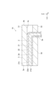
- Fig. 5 is a cross-sectional view of the cable with an electric connector according to the second embodiment.
- Fig. 6 is a cross-sectional view of the cable with an electric connector along line VI-VI shown in Fig. 5.
- the cable with an electric connector 1 according to the second embodiment includes a pair of dielectric constant adjustment sheets 4.
- the outer circumferential surface 21c of each conductor 21 in the tip region 2a of the flat cable 2 is covered by the pair of dielectric constant adjustment sheets 4 while being exposed from the coating 22.
- the tip region 2a of the flat cable 2 is located close to the tip face 3a of the ferrule 3.
- the tip face 22a of the coating 22 is located between the tip face 3a and the rear end face 3b of the ferrule 3.
- a part of the coating 22 is located inside the insertion hole 3c of the ferrule 3.
- the outer circumferential surface 21c of each conductor 21 in the tip region 2a is exposed from the coating 22.
- the pair of dielectric constant adjustment sheets 4 are provided inside the insertion hole 3c of the ferrule 3.
- the pair of dielectric constant adjustment sheets 4 are provided between the tip region 2a and the ferrule 3.
- each conductor 21 is wrapped by the pair of dielectric constant adjustment sheets 4.
- the pair of dielectric constant adjustment sheets 4 are in contact with each other while wrapping each conductor 21.
- the tip surface 4a of the dielectric constant adjustment sheet 4 is located on substantially the same plane as the tip surface 21a of each conductor 21 and the tip surface 3a of the ferrule 3.
- the rear end surface 4b of the dielectric constant adjustment sheet 4 is located between the tip surface 3a and the rear end surface 3b of the ferrule 3.
- the rear end surface 4b of the dielectric constant adjustment sheet 4 is in contact with the tip surface 22a of the coating 22.
- the tip surface 21a of each conductor 21 in the tip region 2a is exposed from the pair of dielectric constant adjustment sheets 4. In other words, the tip surface 21a of each conductor 21 is not covered by the pair of dielectric constant adjustment sheets 4.
- the tip surface 21a of each conductor 21 in the tip region 2a and the tip surface 4a of the dielectric constant adjustment sheet 4 are exposed from the ferrule 3. In other words, the tip surface 21a of each conductor 21 and the tip surface 4a of the dielectric constant adjustment sheet 4 are not covered by the ferrule 3.
- the dielectric constant adjustment sheet 4 is mainly composed of, for example, polypropylene.
- the relative dielectric constant of the dielectric constant adjustment sheet 4 is smaller than the relative dielectric constant of the ferrule 3.
- the relative dielectric constant of the dielectric constant adjustment sheet 4 is, for example, about 2.2.
- the relative dielectric constant of the dielectric constant adjustment sheet 4 is 0.9 times or more and 1.1 times or less than the relative dielectric constant of the insulating layer 221 (see FIG. 3) of the coating 22.
- the dielectric constant of the periphery of the region of the conductor 21 covered by the coating 22 is different from the dielectric constant of the periphery of the region of the conductor 21 exposed from the coating 22.
- the outer peripheral surface 21c of each conductor 21 in the tip region 2a is covered by a pair of dielectric constant adjustment sheets 4, so that unevenness in the dielectric constant distribution around the conductor 21 is suppressed.
- the tip surface 21a of each conductor 21 in the tip region 2a is exposed from the tip surface 4a of the dielectric constant adjustment sheet 4 and the ferrule 3.
- each conductor 21 is electrically connected to the mating connector, and stubs are suppressed compared to, for example, when the outer peripheral surface 21c of the conductor 21 in the tip region 2a is exposed and the conductor 21 is electrically connected to the mating connector via a conductor electrically connected to the outer peripheral surface 21c of the exposed portion. Therefore, both the deterioration of communication performance caused by impedance mismatch and the deterioration of communication performance caused by the stub phenomenon are prevented. Therefore, the cable with electrical connector 1 can prevent degradation of communication performance.
- [Modification] 7 is a cross-sectional view of the cable with an electric connector according to the first modification.
- the tip region 2a of the flat cable 2 may be bent inside the ferrule 3.
- the ferrule 3 further includes an insertion hole 3e that opens in a side surface 3d that intersects with the Z-axis direction.
- the side surface 3d and the insertion hole 3e are formed in, for example, the second holding member 32.
- the insertion hole 3e communicates with the insertion hole 3c.
- the insertion hole 3c extends along the Y-axis direction, and the insertion hole 3e extends along the Z-axis direction.
- the tip region 2a of the flat cable 2 is disposed in both the insertion hole 3c and the insertion hole 3e in a state where it is bent, for example, 90 degrees. In this case, the degree of freedom of arrangement of the cable with an electric connector 1A is improved.
- FIG. 8 is a front view of the cable with an electric connector of the second modified example.
- the cable with an electric connector 1B of the second modified example may include a plurality of flat cables 2.
- the cable with an electric connector 1B may include, for example, two flat cables 2.
- the two flat cables 2 are arranged in parallel, for example, in the Z-axis direction.
- the ferrule 3 may further include a third holding member 33 in addition to the first holding member 31 and the second holding member 32.
- the tip region 2a of each flat cable 2 is disposed between adjacent holding members among the plurality of holding members 31, 32, and 33.
- the third retaining member 33 is disposed between the first retaining member 31 and the second retaining member 32.
- the third retaining member 33 includes a retaining surface 33a, a pair of connecting surfaces 33b, a retaining surface 33c, and a pair of connecting surfaces 33d.
- Each of the holding surface 33a and the connection surface 33b faces the first holding member 31.
- the width of the holding surface 33a in the X-axis direction is the same as the width of the flat cable 2 in the X-axis direction.
- the pair of connection surfaces 33b are located at both ends of the holding surface 33a in the X-axis direction.
- the connection surfaces 33b protrude in the Z-axis direction from the holding surface 33a.
- the connection surfaces 33b are closer to the first holding member 31 than the holding surface 33a.
- Each of the holding surface 33c and the connection surface 33d faces the second holding member 32.
- the width of the holding surface 33c in the X-axis direction is the same as the width of the flat cable 2 in the X-axis direction.
- the pair of connection surfaces 33d are located at both ends of the holding surface 33c in the X-axis direction.
- the connection surface 33d protrudes from the holding surface 33c in the Z-axis direction.
- the connection surface 33d is closer to the second holding member 32 than the holding surface 33c.
- connection surface 31b of the first holding member 31 and the connection surface 33b of the third holding member 33 are connected to each other with the tip region 2a of the first flat cable 2 disposed between the holding surfaces 31a and 33a.
- the tip region 2a of the first flat cable 2 is sandwiched between the first holding member 31 and the third holding member 33.
- the first insertion hole 3c of the ferrule 3 is the space between the holding surfaces 31a and 33a.
- connection surface 32b of the second holding member 32 and the connection surface 33d of the third holding member 33 are connected to each other with the tip region 2a of the second flat cable 2 disposed between the holding surfaces 32a and 33c.
- the tip region 2a of the second flat cable 2 is sandwiched between the second holding member 32 and the third holding member 33.
- the second insertion hole 3c of the ferrule 3 is the space between the holding surfaces 32a and 33c. In the above case, the tip region 2a of each of the multiple flat cables 2 is securely held by the ferrule 3.
- the tip region 2a of each flat cable 2 may be bent inside the ferrule 3, as in the first modified example.
- the ferrule 3 further includes an insertion hole 3e and an insertion hole 3f that open to a side surface 3d that intersects with the Z-axis direction.
- the insertion hole 3e is formed, for example, in the second holding member 32 and the third holding member 33.
- the side surface 3d and the insertion hole 3f are formed, for example, in the second holding member 32.
- the insertion hole 3e communicates with the first insertion hole 3c.
- the insertion hole 3f communicates with the second insertion hole 3c.
- the insertion holes 3e and 3f extend along the Z-axis direction.
- the tip region 2a of the first flat cable 2 is arranged in both the first insertion hole 3c and the insertion hole 3e, for example, in a state where it is bent 90 degrees.
- the tip region 2a of the second flat cable 2 is bent, for example, 90 degrees and placed in both the second insertion hole 3c and the insertion hole 3f. In this case, the degree of freedom in placing the cable with electrical connector 1B is improved.
- the outer circumferential surface 21c of each conductor 21 in the tip region 2a may be covered by a pair of dielectric constant adjustment sheets 4.
- the outer circumferential surface 21c of the conductor 21 in the tip region 2a is covered by a pair of dielectric constant adjustment sheets 4 while being exposed from the coating 22.
- the boundary S between the coating 22 and the dielectric constant adjustment sheet 4 may be provided at a position where the conductor 21 extends in a straight line toward the tip surface 21a (not including a position where the conductor 21 is bent). This allows the conductor 21 and the dielectric constant adjustment sheet 4 to be bonded together flatly by the ferrule 3, making it easier to match the impedance.
- the cable with electrical connector may include three or more flat cables 2.
- the covering 22 of the flat cable 2 may be integrally formed, for example, by extrusion molding using resin.
- the covering 22 may be formed of a pair of resin sheets sandwiching the multiple conductors 21.
- the pair of resin sheets may be bonded to each other. In this case, the spacing between the multiple conductors 21 tends to be uniform when viewed in any cross section perpendicular to the longitudinal direction of each conductor 21.
Landscapes
- Coupling Device And Connection With Printed Circuit (AREA)
Priority Applications (1)
| Application Number | Priority Date | Filing Date | Title |
|---|---|---|---|
| JP2025539339A JPWO2025033292A1 (https=) | 2023-08-10 | 2024-07-31 |
Applications Claiming Priority (2)
| Application Number | Priority Date | Filing Date | Title |
|---|---|---|---|
| JP2023131312 | 2023-08-10 | ||
| JP2023-131312 | 2023-08-10 |
Publications (1)
| Publication Number | Publication Date |
|---|---|
| WO2025033292A1 true WO2025033292A1 (ja) | 2025-02-13 |
Family
ID=94534777
Family Applications (1)
| Application Number | Title | Priority Date | Filing Date |
|---|---|---|---|
| PCT/JP2024/027395 Pending WO2025033292A1 (ja) | 2023-08-10 | 2024-07-31 | 電気コネクタ付ケーブル |
Country Status (2)
| Country | Link |
|---|---|
| JP (1) | JPWO2025033292A1 (https=) |
| WO (1) | WO2025033292A1 (https=) |
Citations (10)
| Publication number | Priority date | Publication date | Assignee | Title |
|---|---|---|---|---|
| JP2002124340A (ja) * | 2000-10-17 | 2002-04-26 | Yazaki Corp | フラットケーブル接続コネクタ |
| JP2002246090A (ja) * | 2001-02-13 | 2002-08-30 | Sunx Ltd | 並列多芯ケーブル用コネクタ |
| JP2004220864A (ja) * | 2003-01-10 | 2004-08-05 | Auto Network Gijutsu Kenkyusho:Kk | フラットケーブルの端末構造 |
| JP2007273418A (ja) * | 2006-03-31 | 2007-10-18 | Fujikura Ltd | フラットハーネス用コネクタ |
| JP2008270014A (ja) * | 2007-04-23 | 2008-11-06 | Molex Inc | フローティングコネクタ |
| JP2009134997A (ja) * | 2007-11-30 | 2009-06-18 | Fujikura Ltd | コネクタ端子構造 |
| JP2009158337A (ja) * | 2007-12-27 | 2009-07-16 | Furukawa Electric Co Ltd:The | 接続コネクタ |
| JP2012178367A (ja) * | 1995-09-29 | 2012-09-13 | Panduit Corp | 複数対の導体の複数の導体を結線するコネクタ |
| JP2014026791A (ja) * | 2012-07-25 | 2014-02-06 | Yazaki Corp | 電線と端子の接続構造 |
| JP2021012890A (ja) * | 2018-10-26 | 2021-02-04 | 株式会社オートネットワーク技術研究所 | コネクタ |
Family Cites Families (2)
| Publication number | Priority date | Publication date | Assignee | Title |
|---|---|---|---|---|
| JPS57143613U (https=) * | 1981-03-05 | 1982-09-09 | ||
| JP2001223047A (ja) * | 2000-02-08 | 2001-08-17 | Yazaki Corp | フラット回路体用の端子及びフラット回路体と端子の接続構造並びにフラット回路体の端末構造 |
-
2024
- 2024-07-31 WO PCT/JP2024/027395 patent/WO2025033292A1/ja active Pending
- 2024-07-31 JP JP2025539339A patent/JPWO2025033292A1/ja active Pending
Patent Citations (10)
| Publication number | Priority date | Publication date | Assignee | Title |
|---|---|---|---|---|
| JP2012178367A (ja) * | 1995-09-29 | 2012-09-13 | Panduit Corp | 複数対の導体の複数の導体を結線するコネクタ |
| JP2002124340A (ja) * | 2000-10-17 | 2002-04-26 | Yazaki Corp | フラットケーブル接続コネクタ |
| JP2002246090A (ja) * | 2001-02-13 | 2002-08-30 | Sunx Ltd | 並列多芯ケーブル用コネクタ |
| JP2004220864A (ja) * | 2003-01-10 | 2004-08-05 | Auto Network Gijutsu Kenkyusho:Kk | フラットケーブルの端末構造 |
| JP2007273418A (ja) * | 2006-03-31 | 2007-10-18 | Fujikura Ltd | フラットハーネス用コネクタ |
| JP2008270014A (ja) * | 2007-04-23 | 2008-11-06 | Molex Inc | フローティングコネクタ |
| JP2009134997A (ja) * | 2007-11-30 | 2009-06-18 | Fujikura Ltd | コネクタ端子構造 |
| JP2009158337A (ja) * | 2007-12-27 | 2009-07-16 | Furukawa Electric Co Ltd:The | 接続コネクタ |
| JP2014026791A (ja) * | 2012-07-25 | 2014-02-06 | Yazaki Corp | 電線と端子の接続構造 |
| JP2021012890A (ja) * | 2018-10-26 | 2021-02-04 | 株式会社オートネットワーク技術研究所 | コネクタ |
Also Published As
| Publication number | Publication date |
|---|---|
| JPWO2025033292A1 (https=) | 2025-02-13 |
Similar Documents
| Publication | Publication Date | Title |
|---|---|---|
| JP7196909B2 (ja) | シールドフラットケーブル | |
| JP3645170B2 (ja) | 電気ケーブル端部構造および電気ケーブル端部処理方法 | |
| US8946556B2 (en) | Shielded flat ribbon cable and method for fabricating a shielded flat ribbon cable | |
| TW201308361A (zh) | 巢式屏蔽之帶狀電纜 | |
| US7534138B1 (en) | Electrical cable shielding terminal | |
| JP7067275B2 (ja) | シールドフラットケーブル | |
| CN110415876B (zh) | 屏蔽扁平线缆 | |
| JP5499722B2 (ja) | シールドフラットケーブル | |
| WO2025033292A1 (ja) | 電気コネクタ付ケーブル | |
| JP6920412B2 (ja) | 電気ケーブル | |
| JP5854008B2 (ja) | フラットケーブル | |
| US20250055226A1 (en) | Electrical-connector-equipped cable | |
| US20250062556A1 (en) | Electrical-connector-equipped flat cable | |
| TWI397085B (zh) | 屏蔽扁平電纜 | |
| CN112384995B (zh) | 扁平电缆以及扁平电缆的制造方法 | |
| US20250062557A1 (en) | Electrical-connector equipped cable | |
| US10700446B2 (en) | Connector | |
| US20240413556A1 (en) | Electrical connector and method for manufacturing electrical connector | |
| US20250062574A1 (en) | Electrical-connector-equipper cable | |
| JP7006489B2 (ja) | シールドフラットケーブル | |
| US12132300B2 (en) | Wiring member | |
| WO2025022990A1 (ja) | ケーブル装置 | |
| JP2025088391A (ja) | コネクタ構造およびコネクタ | |
| CN101662083B (zh) | 带布线基板的电缆组件 | |
| WO2023228861A1 (ja) | フラットケーブル組立体および回転コネクタ装置 |
Legal Events
| Date | Code | Title | Description |
|---|---|---|---|
| 121 | Ep: the epo has been informed by wipo that ep was designated in this application |
Ref document number: 24851717 Country of ref document: EP Kind code of ref document: A1 |
|
| ENP | Entry into the national phase |
Ref document number: 2025539339 Country of ref document: JP Kind code of ref document: A |
|
| WWE | Wipo information: entry into national phase |
Ref document number: 2025539339 Country of ref document: JP |
|
| NENP | Non-entry into the national phase |
Ref country code: DE |