WO2025028302A1 - エッチング方法及びプラズマ処理装置 - Google Patents
エッチング方法及びプラズマ処理装置 Download PDFInfo
- Publication number
- WO2025028302A1 WO2025028302A1 PCT/JP2024/025936 JP2024025936W WO2025028302A1 WO 2025028302 A1 WO2025028302 A1 WO 2025028302A1 JP 2024025936 W JP2024025936 W JP 2024025936W WO 2025028302 A1 WO2025028302 A1 WO 2025028302A1
- Authority
- WO
- WIPO (PCT)
- Prior art keywords
- region
- substrate
- etching method
- gas
- substrate support
- Prior art date
- Legal status (The legal status is an assumption and is not a legal conclusion. Google has not performed a legal analysis and makes no representation as to the accuracy of the status listed.)
- Pending
Links
Images




Classifications
-
- C—CHEMISTRY; METALLURGY
- C23—COATING METALLIC MATERIAL; COATING MATERIAL WITH METALLIC MATERIAL; CHEMICAL SURFACE TREATMENT; DIFFUSION TREATMENT OF METALLIC MATERIAL; COATING BY VACUUM EVAPORATION, BY SPUTTERING, BY ION IMPLANTATION OR BY CHEMICAL VAPOUR DEPOSITION, IN GENERAL; INHIBITING CORROSION OF METALLIC MATERIAL OR INCRUSTATION IN GENERAL
- C23F—NON-MECHANICAL REMOVAL OF METALLIC MATERIAL FROM SURFACE; INHIBITING CORROSION OF METALLIC MATERIAL OR INCRUSTATION IN GENERAL; MULTI-STEP PROCESSES FOR SURFACE TREATMENT OF METALLIC MATERIAL INVOLVING AT LEAST ONE PROCESS PROVIDED FOR IN CLASS C23 AND AT LEAST ONE PROCESS COVERED BY SUBCLASS C21D OR C22F OR CLASS C25
- C23F4/00—Processes for removing metallic material from surfaces, not provided for in group C23F1/00 or C23F3/00
-
- H—ELECTRICITY
- H10—SEMICONDUCTOR DEVICES; ELECTRIC SOLID-STATE DEVICES NOT OTHERWISE PROVIDED FOR
- H10P—GENERIC PROCESSES OR APPARATUS FOR THE MANUFACTURE OR TREATMENT OF DEVICES COVERED BY CLASS H10
- H10P50/00—Etching of wafers, substrates or parts of devices
- H10P50/20—Dry etching; Plasma etching; Reactive-ion etching
- H10P50/24—Dry etching; Plasma etching; Reactive-ion etching of semiconductor materials
- H10P50/242—Dry etching; Plasma etching; Reactive-ion etching of semiconductor materials of Group IV materials
Definitions
- An exemplary embodiment of the present disclosure relates to an etching method and a plasma processing apparatus.
- Patent Document 1 discloses a method for selectively etching a silicon nitride film. This method includes a first step of placing a substrate having a silicon nitride film in a processing space, a second step of introducing a gas containing H and F into the processing space, and a third step of selectively introducing radicals of an inert gas into the processing space.
- This disclosure provides an etching method and plasma processing apparatus that can improve the etching selectivity ratio.
- the etching method includes: (a) providing a substrate on a substrate support in a chamber, the substrate including a first region and a second region, the first region including a first material including at least one selected from the group consisting of silicon oxide and carbon, and the second region including a second material different from the first material; and (b) exposing the substrate to a first plasma generated from a first process gas including hydrogen fluoride without applying an electrical bias to the substrate support.
- an etching method and a plasma processing apparatus are provided that can improve the etching selectivity ratio.
- FIG. 1 is a diagram for explaining an example of the configuration of a plasma processing system.
- FIG. 2 is a diagram for explaining a configuration example of an inductively coupled plasma processing apparatus.
- FIG. 3 is a flow chart of an etching method according to one exemplary embodiment.
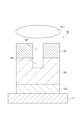
- FIG. 4 is a partial enlarged view of an example substrate to which the method of FIG. 3 may be applied.
- FIG. 5 is a cross-sectional view illustrating a step of an etching method according to an exemplary embodiment.
- FIG. 6 is a cross-sectional view illustrating a step of an etching method according to an exemplary embodiment.
- FIG. 7 is a flow chart of an etching method according to one exemplary embodiment.
- FIG. 1 is a diagram for explaining an example of the configuration of a plasma processing system.
- FIG. 2 is a diagram for explaining a configuration example of an inductively coupled plasma processing apparatus.
- FIG. 3 is a flow chart of an etching method according to one exemplary embodiment.
- FIG. 8 is a graph showing an example of the relationship between the film type and the etching amount.
- FIG. 9 is a partial enlarged view of an example substrate to which the method of FIG. 7 may be applied.
- FIG. 10 is a cross-sectional view illustrating a step of an etching method according to one exemplary embodiment.
- FIG. 11 is a flow chart of an etching method according to one exemplary embodiment.
- FIG. 12 is a partial enlarged view of an example substrate to which the method of FIG. 11 can be applied.
- FIG. 13 is a cross-sectional view illustrating a step of an etching method according to an exemplary embodiment.
- FIG. 14 is a cross-sectional view illustrating a step of an etching method according to one exemplary embodiment.
- FIG. 15 is a cross-sectional view illustrating a step of an etching method according to one exemplary embodiment.
- FIG. 16 is a cross-sectional view illustrating a step of an etching method according to one exemplary embodiment.
- FIG. 17 is a flow chart of an etching method according to one exemplary embodiment.
- FIG. 18 is a cross-sectional view illustrating a step of an etching method according to one exemplary embodiment.
- FIG. 1 is a diagram for explaining an example of the configuration of a plasma processing system.
- the plasma processing system includes a plasma processing device 1 and a control unit 2.
- the plasma processing system is an example of a substrate processing system
- the plasma processing device 1 is an example of a substrate processing device.
- the plasma processing device 1 includes a plasma processing chamber 10, a substrate support unit 11, and a plasma generation unit 12.
- the plasma processing chamber 10 has a plasma processing space.
- the plasma processing chamber 10 also has at least one gas supply port for supplying at least one processing gas to the plasma processing space, and at least one gas exhaust port for exhausting gas from the plasma processing space.
- the gas supply port is connected to a gas supply unit 20 described later, and the gas exhaust port is connected to an exhaust system 40 described later.
- the substrate support unit 11 is disposed in the plasma processing space, and has a substrate support surface for supporting a substrate.
- the inductively coupled plasma processing apparatus 1 includes a plasma processing chamber 10, a gas supply unit 20, a power supply 30, and an exhaust system 40.
- the plasma processing chamber 10 includes a dielectric window 101.
- the plasma processing apparatus 1 also includes a substrate support unit 11, a gas introduction unit, and an antenna 14.
- the substrate support unit 11 is disposed within the plasma processing chamber 10.
- the antenna 14 is disposed on or above the plasma processing chamber 10 (i.e., on or above the dielectric window 101).
- the plasma processing chamber 10 has a plasma processing space 10s defined by the dielectric window 101, a sidewall 102 of the plasma processing chamber 10, and the substrate support unit 11.
- the plasma processing chamber 10 is grounded.
- the power supply 30 may also include a DC power supply 32 coupled to the plasma processing chamber 10.
- the DC power supply 32 includes a bias DC generator 32a.
- the bias DC generator 32a is connected to at least one bias electrode and configured to generate a bias DC signal. The generated bias DC signal is applied to the at least one bias electrode.
- the bias DC signal may be pulsed.
- a sequence of voltage pulses is applied to at least one bias electrode.
- the voltage pulses may have a rectangular, trapezoidal, triangular, or combination of these pulse waveforms.
- a waveform generator for generating a sequence of voltage pulses from the DC signal is connected between the bias DC generator 32a and at least one bias electrode.
- the bias DC generator 32a and the waveform generator constitute a voltage pulse generator.
- the voltage pulses may have a positive polarity or a negative polarity.
- the sequence of voltage pulses may include one or more positive voltage pulses and one or more negative voltage pulses within one period.
- the bias DC generator 32a may be provided in addition to the RF power source 31 or may be provided instead of the second RF generator 31b.
- the exhaust system 40 may be connected to, for example, a gas exhaust port 10e provided at the bottom of the plasma processing chamber 10.
- the exhaust system 40 may include a pressure regulating valve and a vacuum pump. The pressure in the plasma processing space 10s is adjusted by the pressure regulating valve.
- the vacuum pump may include a turbomolecular pump, a dry pump, or a combination thereof.
- FIG. 3 is a flow chart of an etching method according to one exemplary embodiment.
- the etching method MT1 shown in FIG. 3 (hereinafter referred to as "method MT1") can be performed by the plasma processing apparatus 1 of the above embodiment.
- Method MT1 can be applied to the substrate W of FIG. 4.
- the substrate W may include a first region R1 and a second region R2.
- the first region R1 may be a mask.
- the first region R1 may have at least one opening OP.
- the at least one opening OP may be a hole or a slit.
- the first region R1 may have a plurality of openings OP.
- the first region R1 may be a region on the second region R2.
- the second region R2 may be a film to be etched.
- the substrate W may further include a base region UR.
- the second region R2 may be a region on the base region UR.
- the first region R1, the second region R2, and the base region UR may be arranged in this order.
- Each of the first region R1, the second region R2, and the base region UR may be a film.
- the first region R1 includes a first material.
- the first material may include at least one selected from the group consisting of silicon oxide (SiO x ) and carbon, where x is a positive real number.
- the first material may be a carbon-containing material other than fluorocarbon.
- the first material may be at least one carbon-containing material selected from the group consisting of photoresist (polymer) and amorphous carbon.
- the second region R2 includes a second material.
- the second material is different from the first material.
- the second material may include at least one selected from the group consisting of silicon oxide, silicon nitride (SiN x ), silicon oxynitride (SiON), polysilicon, metal, and carbon. x is a positive real number.
- the second material may include at least one metal selected from the group consisting of tungsten (W), molybdenum (Mo), and titanium (Ti).
- the second material may be a compound including a metal element and a nonmetal element.
- the second material may be at least one selected from the group consisting of metal silicide, metal nitride, and metal carbide.
- the second material may be tungsten silicide (WSi).
- the second material may be a fluorocarbon.
- the base region UR may contain metal or silicon.
- Method MT1 will be described below with reference to Figs. 3 to 6, taking as an example a case where method MT1 is applied to a substrate W using the plasma processing apparatus 1 of the above embodiment.
- Figs. 5 to 6 are cross-sectional views showing a step of an etching method according to one exemplary embodiment.
- method MT1 can be performed in the plasma processing apparatus 1 by controlling each part of the plasma processing apparatus 1 by the control unit 2.
- a substrate W on a substrate support 11 arranged in a plasma processing chamber 10 is processed, as shown in Fig. 2.
- method MT1 may include steps ST1 to ST4. Steps ST1 to ST4 may be performed in sequence. Step ST2 may be performed after step ST3. Method MT1 may not include at least one of steps ST2 and ST4.
- Step ST1 a substrate W shown in FIG. 4 is provided on a substrate support 11 in a plasma processing chamber 10.
- Step ST2 In step ST2, as shown in Fig. 5, the substrate W is exposed to a second plasma PL2 generated from a second process gas while an electric bias is supplied to the substrate support 11. This etches the second region R2.
- a recess RS is formed in the second region R2 by the etching.
- the recess RS corresponds to the opening OP in the first region R1.
- the electric bias supplied to the substrate support 11 may be bias RF power or bias DC power.
- the supply of the second process gas may be stopped at the end of step ST2.
- the second process gas may include a fluorocarbon gas.
- An example of the fluorocarbon gas includes C4F6 gas.
- the second process gas may further include an oxygen-containing gas.
- An example of the oxygen-containing gas includes oxygen gas.
- the second process gas may further include at least one inert gas selected from the group consisting of noble gases and nitrogen ( N2 ) gas.
- noble gases include argon (Ar) gas, helium (He) gas, xenon (Xe) gas, and neon (Ne) gas.
- the duration of step ST2 may be 0.1 to 100 seconds, or 10 to 50 seconds.
- the temperature of the substrate support part 11 may be 10°C or higher, 30°C or higher, or 40°C or higher. In step ST2, the temperature of the substrate support part 11 may be 150°C or lower, 120°C or lower, or 80°C or lower.
- the pressure in the plasma processing chamber 10 may be 10 mTorr (1.3 Pa) or more. Also, the pressure in the plasma processing chamber 10 may be 100 mTorr (13 Pa) or less.
- Step ST2 may be performed as follows.
- a second processing gas is supplied into the plasma processing chamber 10 by the gas supply unit 20.
- the control unit 2 controls the gas supply unit 20 and the plasma generation unit 12 so that a second plasma PL2 is generated from the second processing gas.
- the control unit 2 controls the power supply 30 so that an electrical bias is supplied to the substrate support unit 11.
- Step ST3 6 the substrate W is exposed to a first plasma PL1 generated from a first processing gas without supplying an electric bias to the substrate support 11. High-frequency power may not be supplied to the substrate support 11.
- the recess RS may be etched by the first plasma PL1.
- the deposit attached to the opening OP in the process ST2 may be removed by the first plasma PL1.
- the etching residue in the process ST2 may be removed by the first plasma PL1.
- the supply of the first processing gas may be stopped at the end of the process ST3.
- the first process gas is different from the second process gas.
- the first process gas contains hydrogen fluoride gas.
- the first process gas may further contain at least one inert gas selected from the group consisting of noble gases and nitrogen gas.
- the flow rate of hydrogen fluoride gas may be the largest among all the flow rates of gases contained in the first process gas.
- the inert gas that may be contained in the first process gas may be the same as or different from the inert gas contained in the second process gas of step ST2.
- the first process gas may not contain any fluorine-containing gas other than hydrogen fluoride gas.
- the duration of step ST3 may be shorter than the duration of step ST2.
- the duration of step ST3 may be 0.1 to 100 seconds, or 1 to 5 seconds.
- the temperature of the substrate support part 11 may be 10°C or higher, 30°C or higher, or 50°C or higher. In step ST3, the temperature of the substrate support part 11 may be 150°C or lower, or 120°C or lower.
- the pressure in the plasma processing chamber 10 in step ST3 may be greater than the pressure in the plasma processing chamber 10 in step ST2.
- the pressure in the plasma processing chamber 10 may be 10 mTorr (1.3 Pa) or more.
- the pressure in the plasma processing chamber 10 may be 1000 mTorr (130 Pa) or less.
- Step ST3 may be performed as follows.
- a first processing gas is supplied into the plasma processing chamber 10 by the gas supply unit 20.
- the control unit 2 controls the gas supply unit 20 and the plasma generation unit 12 so that a first plasma PL1 is generated from the first processing gas.
- the control unit 2 controls the power supply 30 so that an electrical bias is not supplied to the substrate support unit 11.
- Step ST4 In step ST4, steps ST2 and ST3 are repeated, whereby the etching amount in the second region R2 can be increased, thereby making the recess RS deeper.
- step ST3 etching of the first region R1 is suppressed compared to when an electrical bias is supplied to the substrate support portion 11. As a result, the etching selectivity ratio of the second region R2 to the first region R1 can be improved.
- deposits e.g., deposits containing fluorocarbon
- deposits e.g., deposits containing fluorocarbon
- the flow rate of the gas e.g., oxygen-containing gas
- the gas e.g., oxygen-containing gas
- FIG. 7 is a flowchart of an etching method according to one exemplary embodiment.
- the etching method MT2 shown in FIG. 7 (hereinafter referred to as "method MT2") can be performed by the plasma processing apparatus 1 of the above embodiment.
- Method MT2 can be applied to the substrate W of FIG. 4.
- Method MT2 will be described below with reference to Figures 4, 6 and 7, taking as an example a case where method MT2 is applied to a substrate W using the plasma processing apparatus 1 of the above embodiment.
- method MT2 can be executed in the plasma processing apparatus 1 by controlling each part of the plasma processing apparatus 1 by the control unit 2.
- a substrate W on a substrate support 11 arranged in a plasma processing chamber 10 is processed.
- method MT2 may include steps ST1 and ST3. Steps ST1 and ST3 may be performed in sequence.
- Step ST1) 4 is provided on a substrate support 11 in a plasma processing chamber 10.
- the second material included in the second region R2 may include at least one selected from the group consisting of silicon nitride, silicon oxynitride, polysilicon, and a metal.
- etching of the first region R1 is suppressed in step ST3 compared to when an electrical bias is supplied to the substrate support portion 11.
- the etching selectivity ratio of the second region R2 to the first region R1 can be improved.
- a substrate was provided on a substrate support in a chamber of a plasma processing apparatus (step ST1).
- the substrate had a silicon oxide film and a mask on the silicon oxide film.
- the mask contained amorphous carbon.
- step ST2 while supplying an electrical bias to the substrate support, the silicon oxide film was etched through the openings in the mask by a second plasma generated from a second process gas (step ST2).
- the second process gas was a mixture of fluorocarbon gas, Ar gas, and oxygen gas.
- the temperature of the substrate support in step ST2 was 50°C.
- the duration of step ST2 was 30 seconds.
- step ST3 without supplying an electrical bias to the substrate support, the substrate was exposed to a first plasma generated from a first process gas (step ST3).
- the first process gas was a mixed gas of HF gas and Ar gas.
- the temperature of the substrate support in step ST3 was 60°C.
- the duration of step ST3 was 2 seconds.
- steps ST2 and ST3 were repeated so that each of steps ST2 and ST3 was performed 10 times (number of cycles) (step ST4).
- step ST2 was 25 seconds and step ST4 was carried out so that the number of cycles was 12.
- step ST3 the substrate was exposed to plasma generated from the process gas without supplying an electrical bias to the substrate support.
- the process gas was a mixture of HF gas and Ar gas.
- the temperature of the substrate support in step ST3 was 60°C.
- the duration of step ST3 was 300 seconds.
- Example 7 The seventh experiment was carried out in the same manner as the fifth experiment, except that a substrate having a photoresist film on its surface was used.
- Example 8 The eighth experiment was carried out in the same manner as the fifth experiment, except that a substrate having a polysilicon film on its surface was used.
- Figure 10 is a cross-sectional view showing one step of an etching method according to one exemplary embodiment.
- Step ST3 10 the substrate W is exposed to a first plasma PL1 generated from a first process gas containing hydrogen fluoride gas without supplying an electric bias to the substrate support 11. This etches the second region R2.
- a recess RS is formed in the second region R2 by the etching.
- the underlying region UR can function as an etching stop layer.
- the second portion R12 can be removed, but the first portion R11 is difficult to etch.
- the substrate W further includes a base region UR in addition to the first region R1 and the second region R2.
- the first region R1 and the second region R2 are regions above the base region UR. At least the top R1t of the first region R1 is exposed. At least the top R2t of the second region R2 is exposed.
- the second region R2 is adjacent to the first region R1.
- the second region R2 may be disposed between a pair of first regions R1.
- the pair of first regions R1 and second regions R2 may form a protrusion PT.
- a plurality of protrusions PT may be arranged spaced apart from each other on the base region UR.
- the first region R1 may include at least one selected from the group consisting of silicon oxide and carbon.
- the second region R2 may include at least one selected from the group consisting of silicon nitride, polysilicon, fluorocarbon, and metal.
- the metal that may be included in the second region R2 may include at least one selected from the group consisting of tungsten, molybdenum, niobium (Nb), tantalum (Ta), and titanium.
- the tungsten that may be included in the second region R2 may include at least one selected from the group consisting of WSi x , WC x , WN x , WC x N y , WSi x N y , and WO x , where x and y are positive real numbers.
- Method MT3 will be described below with reference to Figs. 11 to 16, taking as an example a case where method MT3 is applied to the substrate W of Fig. 12 using the plasma processing apparatus 1 of the above embodiment.
- Figs. 13 to 16 are cross-sectional views showing a step of an etching method according to one exemplary embodiment.
- method MT3 can be performed in the plasma processing apparatus 1 by controlling each part of the plasma processing apparatus 1 by the control unit 2.
- a substrate W on a substrate support 11 arranged in a plasma processing chamber 10 is processed, as shown in Fig. 2.
- Step ST1 a substrate W shown in FIG. 12 is provided on a substrate support 11 in a plasma processing chamber 10.
- Step ST3 13 in step ST3, the substrate W is exposed to a first plasma PL1 generated from a first process gas containing hydrogen fluoride gas without supplying an electric bias to the substrate support 11. This etches the second region R2.
- the second region R2 is selectively etched with respect to the first region R1.
- the second region R2 is removed by the etching.
- a plurality of first regions R1 are arranged spaced apart from each other on the base region UR. The supply of the first process gas may be stopped at the end of step ST3.
- etching of the first region R1 is suppressed in step ST3 compared to when an electrical bias is supplied to the substrate support portion 11.
- the etching selectivity ratio of the second region R2 to the first region R1 can be improved.
- Step ST11 the substrate W of FIG. 14 is provided.
- the substrate W includes a base region UR, an etching target film R2a on the base region UR, and a mask MK on the etching target film R2a.
- the etching target film R2a includes a second material included in the second region R2.
- the mask MK includes at least one opening OP1.
- the mask MK may include carbon such as amorphous carbon or SOC (Spin-on Carbon).
- Step ST12 15 in step ST12, the etching target film R2a is etched through an opening OP1 of the mask MK to form a second region R2.
- the second region R2 has an opening OP2 corresponding to the opening OP1.
- the mask MK may be removed.
- Step ST13 In step ST13, as shown in Fig. 16, a first material is deposited on the sidewall of the second region R2 to form the first region R1. After deposition, a portion of the first region R1 may be removed by etching to expose the top portion R2t of the second region R2 and the underlying region UR. In this manner, the substrate W of Fig. 12 is provided.
- the first material can be deposited on the sidewall of the second region R2 by a method such as ALD or MLD.
- ALD atomic layer deposition
- the substrate W is exposed to a process gas containing a silicon-containing precursor (aminosilane, SiCl 4 , SiF 4, etc.). This forms a precursor layer on the surface of the second region R2.
- the substrate W is then exposed to a plasma generated from a process gas containing an oxygen-containing gas (O 2 , CO, CO 2, etc.). This modifies the precursor layer to form a silicon oxide film.
- an oxygen-containing gas O 2 , CO, CO 2, etc.
- the substrate W is then exposed to a second process gas containing a second organic compound different from the first organic compound. This forms an organic film by reaction between the first organic compound and the second organic compound.
- FIG. 17 is a flowchart of an etching method according to one exemplary embodiment.
- the etching method MT4 shown in FIG. 17 (hereinafter referred to as "method MT4") can be performed by the plasma processing apparatus 1 of the above embodiment.
- Method MT4 can be applied to the substrate W of FIG. 12.
- Method MT4 will be described below with reference to Figs. 13, 17 to 18, taking as an example the case where method MT4 is applied to the substrate W of Fig. 12 using the plasma processing apparatus 1 of the above embodiment.
- Fig. 18 is a cross-sectional view showing one step of an etching method according to one exemplary embodiment.
- method MT4 can be performed in the plasma processing apparatus 1 by controlling each part of the plasma processing apparatus 1 by the control unit 2.
- method MT3 as shown in Fig. 2, a substrate W on a substrate support 11 arranged in a plasma processing chamber 10 is processed.
- method MT4 may include steps ST1, ST31, and ST21. Steps ST1, ST31, and ST21 may be performed in order. Step ST31 may be performed after step ST21. Step ST1 may include steps ST11 to ST13. Step ST1 may be performed in the same manner as step ST1 of method MT3.
- Step ST31 may be performed in the same manner as step ST3.
- step ST31 as shown in Fig. 13, the substrate W is exposed to a first plasma PL1 generated from a first process gas containing hydrogen fluoride gas while no electric bias is supplied to the substrate support 11 or an electric bias of a first level is supplied to the substrate support 11. This etches the second region R2.
- the second region R2 is selectively etched with respect to the first region R1.
- the supply of the first process gas may be stopped at the end of step ST31.
- the level of the electrical bias is the power level (effective value) of the bias RF power. If the electrical bias is bias DC power, the bias DC power may include a voltage pulse. In this case, the level of the electrical bias is the absolute value of the negative voltage level of the voltage pulse.
- Step ST21 may be performed in the same manner as step ST2.
- step ST21 as shown in FIG. 18, the substrate W is exposed to a second plasma PL2 generated from a second processing gas while a second level of electric bias is supplied to the substrate support 11.
- the second level is greater than a first level that may be supplied to the substrate support 11 in step ST31.
- the second processing gas may be the same as or different from the first processing gas in step ST31.
- the base region UR may be etched.
- a recess RS1 is formed in the base region UR by etching.
- the recess RS1 corresponds to the opening OP of the first region R1.
- the supply of the second processing gas may be stopped at the end of step ST21.
- step ST31 etching of the first region R1 is suppressed compared to when a high level of electrical bias is supplied to the substrate support portion 11. As a result, the etching selectivity ratio of the second region R2 to the first region R1 can be improved.
- Step ST31 of method MT4 may be performed in step ST3 of methods MT1 to MT3. That is, a first level of electrical bias may be supplied to the substrate support 11 in step ST3 of methods MT1 to MT3.
- step ST21 of method MT4 may be performed in step ST2 of method MT1.
- a second level of electrical bias may be supplied to the substrate support 11 in step ST2 of method MT1.
- [E1] (a) providing a substrate on a substrate support in a chamber, the substrate comprising a first region and a second region, the first region comprising a first material comprising at least one selected from the group consisting of silicon oxide and carbon, and the second region comprising a second material different from the first material; (b) exposing the substrate to a first plasma generated from a first process gas comprising hydrogen fluoride without applying an electrical bias to the substrate support;
- An etching method comprising:
Landscapes
- Chemical & Material Sciences (AREA)
- Engineering & Computer Science (AREA)
- Materials Engineering (AREA)
- Mechanical Engineering (AREA)
- Metallurgy (AREA)
- Organic Chemistry (AREA)
- Drying Of Semiconductors (AREA)
- Physics & Mathematics (AREA)
- Plasma & Fusion (AREA)
- Analytical Chemistry (AREA)
Priority Applications (3)
| Application Number | Priority Date | Filing Date | Title |
|---|---|---|---|
| KR1020267005048A KR20260048572A (ko) | 2023-08-02 | 2024-07-19 | 에칭 방법 및 플라즈마 처리 장치 |
| JP2025537844A JPWO2025028302A1 (https=) | 2023-08-02 | 2024-07-19 | |
| CN202480047889.0A CN121647062A (zh) | 2023-08-02 | 2024-07-19 | 蚀刻方法及等离子体处理装置 |
Applications Claiming Priority (2)
| Application Number | Priority Date | Filing Date | Title |
|---|---|---|---|
| JP2023-126149 | 2023-08-02 | ||
| JP2023126149 | 2023-08-02 |
Publications (1)
| Publication Number | Publication Date |
|---|---|
| WO2025028302A1 true WO2025028302A1 (ja) | 2025-02-06 |
Family
ID=94395219
Family Applications (1)
| Application Number | Title | Priority Date | Filing Date |
|---|---|---|---|
| PCT/JP2024/025936 Pending WO2025028302A1 (ja) | 2023-08-02 | 2024-07-19 | エッチング方法及びプラズマ処理装置 |
Country Status (5)
| Country | Link |
|---|---|
| JP (1) | JPWO2025028302A1 (https=) |
| KR (1) | KR20260048572A (https=) |
| CN (1) | CN121647062A (https=) |
| TW (1) | TW202520374A (https=) |
| WO (1) | WO2025028302A1 (https=) |
Citations (5)
| Publication number | Priority date | Publication date | Assignee | Title |
|---|---|---|---|---|
| JP2015216208A (ja) * | 2014-05-09 | 2015-12-03 | 東京エレクトロン株式会社 | エッチング方法 |
| JP2016513883A (ja) * | 2013-03-15 | 2016-05-16 | アプライド マテリアルズ インコーポレイテッドApplied Materials,Incorporated | 極端な共形性を有するカーボンフィルム堆積、背景技術 |
| US20160307773A1 (en) * | 2015-04-15 | 2016-10-20 | Samsung Electronics Co., Ltd. | Method of Manufacturing Semiconductor Devices |
| JP2022084004A (ja) * | 2020-11-25 | 2022-06-06 | 東京エレクトロン株式会社 | 基板処理方法及び基板処理装置 |
| JP2023055335A (ja) * | 2021-10-06 | 2023-04-18 | 東京エレクトロン株式会社 | エッチング方法及びエッチング装置 |
Family Cites Families (4)
| Publication number | Priority date | Publication date | Assignee | Title |
|---|---|---|---|---|
| US6884722B2 (en) * | 2001-09-27 | 2005-04-26 | International Business Machines Corporation | Method of fabricating a narrow polysilicon line |
| US9553102B2 (en) * | 2014-08-19 | 2017-01-24 | Applied Materials, Inc. | Tungsten separation |
| US10483109B2 (en) * | 2016-04-12 | 2019-11-19 | Tokyo Electron Limited | Self-aligned spacer formation |
| JP6689159B2 (ja) * | 2016-08-22 | 2020-04-28 | 東京エレクトロン株式会社 | エッチング方法およびdramキャパシタの製造方法 |
-
2024
- 2024-07-19 WO PCT/JP2024/025936 patent/WO2025028302A1/ja active Pending
- 2024-07-19 CN CN202480047889.0A patent/CN121647062A/zh active Pending
- 2024-07-19 TW TW113127069A patent/TW202520374A/zh unknown
- 2024-07-19 JP JP2025537844A patent/JPWO2025028302A1/ja active Pending
- 2024-07-19 KR KR1020267005048A patent/KR20260048572A/ko active Pending
Patent Citations (5)
| Publication number | Priority date | Publication date | Assignee | Title |
|---|---|---|---|---|
| JP2016513883A (ja) * | 2013-03-15 | 2016-05-16 | アプライド マテリアルズ インコーポレイテッドApplied Materials,Incorporated | 極端な共形性を有するカーボンフィルム堆積、背景技術 |
| JP2015216208A (ja) * | 2014-05-09 | 2015-12-03 | 東京エレクトロン株式会社 | エッチング方法 |
| US20160307773A1 (en) * | 2015-04-15 | 2016-10-20 | Samsung Electronics Co., Ltd. | Method of Manufacturing Semiconductor Devices |
| JP2022084004A (ja) * | 2020-11-25 | 2022-06-06 | 東京エレクトロン株式会社 | 基板処理方法及び基板処理装置 |
| JP2023055335A (ja) * | 2021-10-06 | 2023-04-18 | 東京エレクトロン株式会社 | エッチング方法及びエッチング装置 |
Also Published As
| Publication number | Publication date |
|---|---|
| CN121647062A (zh) | 2026-03-10 |
| JPWO2025028302A1 (https=) | 2025-02-06 |
| KR20260048572A (ko) | 2026-04-10 |
| TW202520374A (zh) | 2025-05-16 |
Similar Documents
| Publication | Publication Date | Title |
|---|---|---|
| TW202316520A (zh) | 蝕刻方法及蝕刻裝置 | |
| JP7721455B2 (ja) | プラズマ処理方法及びプラズマ処理システム | |
| WO2024043139A1 (ja) | エッチング方法及びプラズマ処理装置 | |
| WO2023127820A1 (ja) | エッチング方法及びプラズマ処理装置 | |
| TW202243000A (zh) | 基板處理方法及基板處理裝置 | |
| WO2025028302A1 (ja) | エッチング方法及びプラズマ処理装置 | |
| WO2024117212A1 (ja) | エッチング方法及びプラズマ処理装置 | |
| JP2023170855A (ja) | エッチング方法及びプラズマ処理装置 | |
| WO2023233673A1 (ja) | エッチング方法及びプラズマ処理装置 | |
| JP2023109497A (ja) | エッチング方法及びプラズマ処理装置 | |
| TW202520375A (zh) | 蝕刻方法及電漿處理裝置 | |
| JP7664139B2 (ja) | エッチング方法及びプラズマ処理装置 | |
| JP2026002318A (ja) | エッチング方法及びプラズマ処理装置 | |
| JP2024094240A (ja) | エッチング方法及びプラズマ処理装置 | |
| TW202449899A (zh) | 蝕刻方法及電漿處理裝置 | |
| WO2024203479A1 (ja) | エッチング方法及びプラズマ処理装置 | |
| JP2024064179A (ja) | エッチング方法及びプラズマ処理装置 | |
| WO2025173580A1 (ja) | エッチング方法、及び、プラズマ処理装置 | |
| WO2024090252A1 (ja) | 基板処理方法及び基板処理装置 | |
| CN118263113A (zh) | 蚀刻方法及等离子体处理装置 | |
| JP2024033846A (ja) | 基板処理方法及びプラズマ処理装置 | |
| JP2025089743A (ja) | エッチング方法 | |
| JP2025026361A (ja) | エッチング方法及びプラズマ処理装置 | |
| WO2026070509A1 (ja) | エッチング方法及びプラズマ処理装置 | |
| WO2025173577A1 (ja) | エッチング方法、及び、プラズマ処理装置 |
Legal Events
| Date | Code | Title | Description |
|---|---|---|---|
| 121 | Ep: the epo has been informed by wipo that ep was designated in this application |
Ref document number: 24848957 Country of ref document: EP Kind code of ref document: A1 |
|
| ENP | Entry into the national phase |
Ref document number: 2025537844 Country of ref document: JP Kind code of ref document: A |
|
| WWE | Wipo information: entry into national phase |
Ref document number: 2025537844 Country of ref document: JP |
|
| ENP | Entry into the national phase |
Ref document number: 1020267005048 Country of ref document: KR Free format text: ST27 STATUS EVENT CODE: A-0-1-A10-A15-NAP-PA0105 (AS PROVIDED BY THE NATIONAL OFFICE) |
|
| WWE | Wipo information: entry into national phase |
Ref document number: 11202600328W Country of ref document: SG |
|
| WWP | Wipo information: published in national office |
Ref document number: 11202600328W Country of ref document: SG |
|
| NENP | Non-entry into the national phase |
Ref country code: DE |