WO2025027443A1 - コンピュータ、情報処理装置、サーバ、及び記憶装置 - Google Patents
コンピュータ、情報処理装置、サーバ、及び記憶装置 Download PDFInfo
- Publication number
- WO2025027443A1 WO2025027443A1 PCT/IB2024/057074 IB2024057074W WO2025027443A1 WO 2025027443 A1 WO2025027443 A1 WO 2025027443A1 IB 2024057074 W IB2024057074 W IB 2024057074W WO 2025027443 A1 WO2025027443 A1 WO 2025027443A1
- Authority
- WO
- WIPO (PCT)
- Prior art keywords
- layer
- conductive layer
- transistor
- insulating layer
- oxide semiconductor
- Prior art date
- Legal status (The legal status is an assumption and is not a legal conclusion. Google has not performed a legal analysis and makes no representation as to the accuracy of the status listed.)
- Pending
Links
Images


Classifications
-
- H—ELECTRICITY
- H10—SEMICONDUCTOR DEVICES; ELECTRIC SOLID-STATE DEVICES NOT OTHERWISE PROVIDED FOR
- H10B—ELECTRONIC MEMORY DEVICES
- H10B12/00—Dynamic random access memory [DRAM] devices
-
- H—ELECTRICITY
- H10—SEMICONDUCTOR DEVICES; ELECTRIC SOLID-STATE DEVICES NOT OTHERWISE PROVIDED FOR
- H10B—ELECTRONIC MEMORY DEVICES
- H10B41/00—Electrically erasable-and-programmable ROM [EEPROM] devices comprising floating gates
- H10B41/70—Electrically erasable-and-programmable ROM [EEPROM] devices comprising floating gates the floating gate being an electrode shared by two or more components
-
- H—ELECTRICITY
- H10—SEMICONDUCTOR DEVICES; ELECTRIC SOLID-STATE DEVICES NOT OTHERWISE PROVIDED FOR
- H10B—ELECTRONIC MEMORY DEVICES
- H10B53/00—Ferroelectric RAM [FeRAM] devices comprising ferroelectric memory capacitors
- H10B53/30—Ferroelectric RAM [FeRAM] devices comprising ferroelectric memory capacitors characterised by the memory core region
Definitions
- One aspect of the present invention relates to a semiconductor device.
- One aspect of the present invention relates to a memory device.
- One aspect of the present invention relates to an arithmetic processing device.
- One aspect of the present invention relates to a semiconductor device having a memory device and an arithmetic processing device.
- One aspect of the present invention relates to a computer, an information processing device, and a server.
- one embodiment of the present invention is not limited to the above technical field.
- Examples of technical fields of one embodiment of the present invention disclosed in this specification and the like include semiconductor devices, display devices, light-emitting devices, power storage devices, memory devices, electronic devices, lighting devices, input devices, input/output devices, driving methods thereof, and manufacturing methods thereof.
- a semiconductor device refers to any device that can function by utilizing semiconductor characteristics.
- Smartphones, tablet devices, personal computers, servers, and other computers incorporate various processors such as a CPU (Central Processing Unit) and a GPU (Graphics Processing Unit), as well as memory devices.
- processors such as a CPU (Central Processing Unit) and a GPU (Graphics Processing Unit), as well as memory devices.
- memory devices such as SRAM (Static Random Access Memory), DRAM (Dynamic Random Access Memory), and NAND memory, which are suitable for high-speed operation and can easily be made large-capacity.
- computers incorporate multiple types of memory devices.
- Patent Document 1 discloses a nonvolatile memory device to which an OS transistor is applied.
- Patent Document 2 discloses a memory device to which a vertical OS transistor is applied.
- DRAM one of the memory devices used in many computers, stores information by storing electric charge input via transistors in a capacitor.
- the charge in the capacitor is lost, so the data must be rewritten each time it is read.
- the data retention period is short, and a write operation (refresh operation) must be performed repeatedly at regular intervals, requiring a large amount of power just to retain the data.
- DRAM is also used in large-scale AI servers, and so when viewed worldwide, its power consumption may be at a level that has an impact on global warming.
- An object of one embodiment of the present invention is to provide a memory device, an arithmetic processing device, a semiconductor device, or an information processing device with reduced power consumption.
- An object of one embodiment of the present invention is to provide a memory device that can be highly integrated, or an arithmetic processing device, a semiconductor device, or an information processing device that includes such a memory device.
- An object of one embodiment of the present invention is to provide a memory device, an arithmetic processing device, a semiconductor device, or an information processing device that generates a small amount of heat.
- An object of one embodiment of the present invention is to provide a highly reliable storage device, arithmetic processing device, semiconductor device, or information processing device.
- An object of one embodiment of the present invention is to provide a storage device, arithmetic processing device, semiconductor device, or information processing device having a new configuration.
- An object of one embodiment of the present invention is to at least alleviate at least one of the problems of the prior art.
- One aspect of the present invention is an information processing device having first to third layers.
- the first layer has a processor
- the second layer has a first memory cell
- the third layer has a second memory cell.
- the first memory cell is composed of a first transistor and a second transistor.
- the second transistor has a gate connected to one of the source and drain of the first transistor.
- the second memory cell is composed of a third transistor, a fourth transistor, and a capacitor.
- the fourth transistor has a gate connected to one of the source and drain of the third transistor and one electrode of the capacitor.
- the first to fourth transistors each have an oxide semiconductor in the channel, and are vertical transistors whose source and drain are located at different heights.
- the second layer is located between the first layer and the third layer.
- the second layer is located on the first layer, and the third layer is located on the second layer.
- the first layer is located on the second layer, and the second layer is located on the third layer.
- the first layer has a first processor
- the second layer has a first memory cell
- the third layer has a second memory cell
- the fourth layer has a second processor
- the fifth layer has a NAND memory.
- the first memory cell is composed of a first transistor and a second transistor.
- the second transistor has a gate connected to one of the source and drain of the first transistor.
- the second memory cell is composed of a third transistor, a fourth transistor, and a capacitance.
- the fourth transistor has a gate connected to one of the source and drain of the third transistor and one electrode of the capacitance.
- the first to fourth transistors each have an oxide semiconductor in the channel and are vertical transistors whose source and drain are located at different heights.
- the second layer is located between the first layer and the fifth layer, and between the fourth layer and the fifth layer.
- the third layer is located between the second layer and the fifth layer.
- the first processor is a CPU and the second processor is a GPU.
- Another aspect of the present invention is an information processing device according to any one of the above, characterized in that it does not have a DRAM.
- Another aspect of the present invention is a computer having a housing in which the above-mentioned information processing device is mounted and a display unit.
- Another aspect of the present invention is a server having a motherboard on which the above-mentioned information processing device is mounted and a rack for storing the motherboard.
- Another aspect of the present invention includes a first transistor, a second transistor, a capacitor, a first insulating layer, and a second insulating layer, the first transistor having a first conductive layer, a second conductive layer, a third conductive layer, a third insulating layer, and a first oxide semiconductor layer, the second transistor having a third conductive layer, a fourth conductive layer, a fifth conductive layer, a sixth conductive layer, a fourth insulating layer, a fifth insulating layer, and a second oxide semiconductor layer, the capacitor having a third conductive layer, a sixth insulating layer, and a fourth conductive layer, the first insulating layer having a first opening reaching the first conductive layer, the second conductive layer being located on the first insulating layer, the first oxide semiconductor layer being in contact with an upper surface of the second conductive layer and in contact with the first conductive layer through the first opening, and the third insulating layer being in contact with the first conductive layer.
- the fifth insulating layer is located inside the first oxide semiconductor layer in the opening, the third conductive layer is located inside the third insulating layer in the first opening, the sixth insulating layer is located on the third conductive layer, the fourth conductive layer is located on the sixth insulating layer, the second insulating layer is located on the fourth conductive layer, the sixth insulating layer, the fourth conductive layer, and the second insulating layer have a second opening that reaches the third conductive layer, the fifth conductive layer is located on the second insulating layer, the fourth insulating layer is in contact with at least the fourth conductive layer in the second opening, the second oxide semiconductor layer is in contact with the upper surface of the fifth conductive layer and is in contact with the third conductive layer through the second opening, the fifth insulating layer is located inside the second oxide semiconductor layer in the second opening, and the sixth conductive layer is located inside the fifth insulating layer in the second opening.
- the shortest distance between the upper surface of the third conductive layer and the lower surface of the fourth conductive layer is shorter than the shortest distance between the upper surface of the fourth conductive layer and the lower surface of the fifth conductive layer.
- the first conductive layer has a first recess, the first opening overlaps the first recess, and the first oxide semiconductor layer contacts the bottom and side surfaces of the first recess.
- the third conductive layer has a second recess, the second opening overlaps the second recess, and the second oxide semiconductor layer contacts the bottom and side surfaces of the second recess.
- the first opening and the second opening are circular in plan view.
- the first opening and the second opening have centers at different positions when viewed in a plan view.
- a memory device an arithmetic processing device, a semiconductor device, or an information processing device with reduced power consumption.
- a memory device that can be highly integrated, or an arithmetic processing device, a semiconductor device, or an information processing device that includes the memory device.
- the present invention it is possible to provide a highly reliable storage device, arithmetic processing device, semiconductor device, or information processing device. Or, it is possible to provide a storage device, arithmetic processing device, semiconductor device, or information processing device having a new configuration. Furthermore, according to one aspect of the present invention, it is possible to at least alleviate at least one of the problems of the prior art.
- FIG. 1A and 1B show an example of the configuration of a semiconductor device.
- 2A and 2B show examples of the configuration of a semiconductor device.
- 3A and 3B are diagrams for explaining the hierarchy of memory devices in a semiconductor device.
- 4A to 4C are diagrams for explaining the hierarchy of memory devices in a semiconductor device.
- FIG. 5A shows an example of the configuration of a processor
- FIG. 5B shows an example of the configuration of a GPU.
- 6A and 6B show examples of the configuration of a storage device.
- 7A and 7B show examples of the configuration of a storage device.
- 8A to 8E show examples of the configuration of a storage device.
- 9A and 9B are circuit diagrams showing an example of a memory device, and FIGS.
- FIG. 10 is a cross-sectional view showing an example of a storage device.
- FIG. 11 is a cross-sectional view showing an example of a storage device.
- FIG. 12 is a cross-sectional view showing an example of a storage device.
- FIG. 13 is a cross-sectional view showing an example of a storage device.
- FIG. 14 is a cross-sectional view showing an example of a storage device.
- FIG. 15 is a cross-sectional view showing an example of a storage device.
- FIG. 16 is a cross-sectional view showing an example of a storage device.
- 17A to 17C are plan views showing an example of a storage device.
- FIG. 18 is a cross-sectional view showing an example of a storage device.
- FIG. 19 is a cross-sectional view showing an example of a storage device.
- FIG. 20 is a cross-sectional view showing an example of a storage device.
- 21A to 21C are cross-sectional views showing an example of a memory device.
- FIG. 22 is a cross-sectional view showing an example of a storage device.
- FIG. 23 is a cross-sectional view showing an example of a storage device.
- FIG. 24 is a cross-sectional view showing an example of a storage device.
- FIG. 25 is a cross-sectional view showing an example of a storage device.
- FIG. 26 is a cross-sectional view showing an example of a storage device.
- FIG. 27 is a cross-sectional view showing an example of a storage device.
- FIG. 28 is a block diagram illustrating an example of the configuration of a storage device.
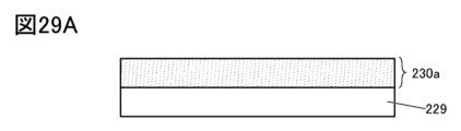
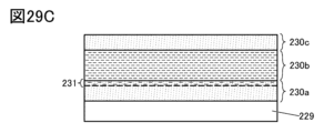
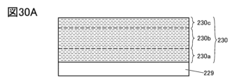
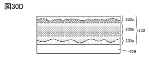
- 29A to 29D are cross-sectional views illustrating a method for forming a metal oxide film.
- 30A to 30D are cross-sectional views illustrating a method for forming a metal oxide film.
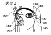
- 31A to 31J show configuration examples of electronic devices.
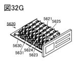
- 32A to 32H show configuration examples of electronic devices.
- a transistor that uses an oxide semiconductor or a metal oxide in a semiconductor layer and a transistor that has an oxide semiconductor or a metal oxide in a channel formation region may be referred to as an OS transistor.
- a transistor that has silicon in a channel formation region may be referred to as a Si transistor.
- an oxynitride refers to a material whose composition contains more oxygen than nitrogen.
- An oxynitride refers to a material whose composition contains more nitrogen than oxygen.
- film and “layer” can be interchanged depending on the circumstances.
- conductive layer can be changed to the term “conductive film.”
- insulating film can be changed to the term “insulating layer.”
- parallel refers to a state in which two straight lines are arranged at an angle of -10 degrees or more and 10 degrees or less. Therefore, it also includes cases in which the angle is -5 degrees or more and 5 degrees or less.
- approximately parallel refers to a state in which two straight lines are arranged at an angle of -20 degrees or more and 20 degrees or less.
- Perfect refers to a state in which two straight lines are arranged at an angle of 80 degrees or more and 100 degrees or less. Therefore, it also includes cases in which the angle is 85 degrees or more and 95 degrees or less.
- approximately perpendicular refers to a state in which two straight lines are arranged at an angle of 70 degrees or more and 110 degrees or less.
- electrically connected includes cases where the connection is made via "something that has some kind of electrical action.”
- something that has some kind of electrical action is not particularly limited as long as it allows the transmission and reception of electrical signals between the connected objects.
- something that has some kind of electrical action includes electrodes or wiring, as well as switching elements such as transistors, resistive elements, coils, and other elements with various functions.
- the off-state current refers to leakage current between the source and drain when a transistor is in an off state (also referred to as a non-conducting state or a cut-off state).
- the off state refers to a state in which the voltage Vgs between the gate and source of an n-channel transistor is lower than the threshold voltage Vth (higher than Vth for a p-channel transistor).
- the normally-on characteristic refers to a state in which a channel exists and current flows through the transistor even when no voltage is applied to the gate.
- the normally-off characteristic refers to a state in which no current flows through the transistor when no potential is applied to the gate or when a ground potential is applied to the gate.
- arrows indicating the X direction, Y direction, and Z direction may be used.
- the "X direction” is the direction along the X axis, and unless explicitly stated, no distinction is made between the forward direction and the reverse direction. The same applies to the "Y direction” and "Z direction.”
- the X direction, Y direction, and Z direction are directions that intersect with each other.
- the X direction, Y direction, and Z direction are directions that are perpendicular to each other.
- the semiconductor device according to one embodiment of the present invention includes a processor and a memory device.
- the semiconductor device according to one embodiment of the present invention can hold data and process the data (arithmetic processing). Therefore, one embodiment of the present invention can also be called an arithmetic processing device or an information processing device. In this specification and the like, the semiconductor device can be replaced with an arithmetic processing device or an information processing device unless otherwise specified.
- NOSRAM a memory device referred to as a NOSRAM, which will be described below, is used as the semiconductor device of one embodiment of the present invention. Therefore, the semiconductor device of one embodiment of the present invention can also be called a device using a NOSRAM.
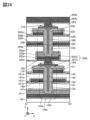
- FIG. 1A is a schematic perspective view of a semiconductor device 10 according to one embodiment of the present invention.
- FIG. 1B is a schematic perspective view showing each layer of the semiconductor device 10 in isolation.
- the semiconductor device 10 has a layered structure in which five layers are stacked.
- the semiconductor device 10 has a configuration in which layers 11, 12, 13, 14, and 15 are stacked in this order.
- Layer 11 and layer 12 each have a processor.
- layer 11 is a layer having a GPU
- layer 12 is a layer having a CPU. Note that, if the CPU and GPU are formed side-by-side on the same plane, layers 11 and 12 may be combined into one layer. Also, the stacking order of layers 11 and 12 is not limited to this, and layer 11 having a GPU may be stacked on layer 12 having a CPU.
- Layer 13 is a layer having a memory array.
- the memory array of layer 13 has a plurality of memory cells 20 arranged in a matrix.
- the memory cells 20 may be stacked not only in the in-plane direction of the layer but also in the thickness direction of the layer, and may be arranged in a three-dimensional matrix.
- memory cell 20 is composed of two transistors.
- Memory cell 20 has a configuration in which the gate of one transistor is connected to either the source or drain of the other transistor.
- layer 14 is a layer having a memory array.
- the memory array of layer 14 has a plurality of memory cells 30.
- memory cells 30 may also be stacked not only in the in-plane direction of the layer but also in the thickness direction of the layer, and may be arranged in a three-dimensional matrix.
- memory cell 30 is composed of two transistors and one capacitor (also called a capacitive element).
- Memory cell 30 has a configuration in which the gate of one transistor is connected to one of the source and drain of the other transistor and one electrode of the capacitor.
- FIG. 1B also shows an example in which the other transistor has a backgate (second gate) that is connected to the other electrode of the capacitor.
- Memory cell 20 provided in layer 13 and memory cell 30 provided in layer 14 have a common connection relationship between two transistors. That is, the gate of one of the two transistors is connected to either the source or drain of the other transistor.
- a memory having such a configuration, and in particular using an oxide semiconductor in the channel of at least one of the transistors, can be called a NOSRAM (Nonvolatile Oxide Semiconductor RAM). Unlike DRAM, one of the features of NOSRAM is that it allows nondestructive readout.
- memory cells 20 and 30 The main difference between memory cells 20 and 30 is whether they have capacity or not.
- Memory cells 20, which do not have capacity can be used to increase the drive speed (particularly the data write speed), and therefore can be used as a memory region that is accessed frequently.
- memory cells 30, which have capacity can be used to increase the data retention period, although their drive speed is inferior to that of memory cells 20, and therefore can be used as a memory region that is accessed less frequently than memory cells 20.
- Layer 15 has a memory array in which multiple memory strings 40 are arranged. As shown in FIG. 1B, memory string 40 has a configuration in which multiple cell transistors are connected in series. Each cell transistor is a transistor that can hold one or more bits of data. As the cell transistor, a transistor with a charge storage layer, a transistor with a ferroelectric layer, a transistor with a floating gate, etc. can be used.
- the memory string 40 in layer 15 is a so-called non-volatile memory with an extremely long data retention period.
- Layer 15 has a structure that is easy to integrate three-dimensionally, so it can be used as a storage device with an extremely large data capacity.
- the write and read speeds are slower than memory cells 20 and 30. Therefore, layer 15 can be suitably used as a memory area that is accessed even less frequently than layer 14.
- layers with memory with faster drive speeds are arranged closer to layers 11 and 12 that have the processor, and layers with memory with longer data retention periods are arranged farther away from layers 11 and 12.
- layers with memory with longer data retention periods are arranged farther away from layers 11 and 12.
- Methods for bonding each layer include wire bonding using gold or copper wiring, flip chip bonding using bumps, or direct bonding (hybrid bonding) using a direct bonding technique such as Cu-Cu bonding.
- a method may be used in which two or more layers are bonded together with insulating films, and then through electrodes are formed to connect the electrodes provided on each layer.
- the pitch of the connection electrodes can be made extremely narrow, making it possible to arrange a large number of connection electrodes at high density, which is preferable because it increases the amount of data transmitted between layers.
- any of CoC (chip on chip) bonding, CoW (chip on wafer) bonding, and WoW (wafer on wafer) bonding may be used.
- WoW bonding is highly productive because it bonds wafers together, but it may reduce yields because all chips, including both good and bad, are bonded together.
- CoW bonding, which bonds chips to wafers, and CoC bonding, which bonds chips together are inferior to WoW bonding in terms of productivity, but the yield is significantly improved because good chips can be bonded together.
- CoC bonding is also less productive than the other two, but is versatile because it can be used to bond two layers even when the sizes are significantly different.
- the semiconductor device 10A shown in Figures 2A and 2B is an example in which the stacking order of the layers in the semiconductor device 10 is reversed.
- the semiconductor device 10A is stacked in the order of layer 15, layer 14, layer 13, layer 12, and layer 11.
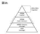
- Figure 3A shows the hierarchy of a conventional memory device.
- Figure 3A shows a register as memory integrated into a processor such as a CPU or GPU, and shows examples of using SRAM for cache memory, DRAM for main memory, and NAND memory and HDD (Hard Disk Drive) for storage.
- a processor such as a CPU or GPU
- SRAM static random access memory
- DRAM dynamic random access memory
- HDD Hard Disk Drive
- Memory integrated into processors such as CPUs and GPUs is used for temporary storage of calculation results, and is therefore accessed frequently by the arithmetic processing unit. Therefore, faster operating speeds are required rather than memory capacity.
- Registers also have the function of storing setting information for the arithmetic processing unit.
- a cache has the function of duplicating and storing a portion of the data held in the main memory. By duplicating frequently used data and storing it in the cache, the speed of access to the data can be increased.
- the storage capacity required for a cache is less than that of main memory, but it is required to have a faster operating speed than main memory.
- data that is rewritten in the cache is duplicated and supplied to the main memory.
- Main memory has the function of holding programs, data, etc. read from storage.
- Storage has the function of holding data that requires long-term storage and various programs used by processing units. Therefore, storage requires a larger memory capacity and a higher recording density than an operating speed.
- NAND type memory such as 3D NAND
- high-capacity, non-volatile storage devices such as HDDs can be used.
- At least the DRAM used as the main memory is replaced with a storage device using an oxide semiconductor (OS memory).
- OS memory oxide semiconductor
- DRAM requires a refresh operation and is a destructive readout storage device, and therefore consumes much more power than other storage devices. Therefore, by not using DRAM, power consumption can be significantly reduced.
- the range of various storage devices that is targeted for replacement with OS memory is indicated by a dashed line. In other words, not only the DRAM used as the main memory, but also the SRAM used as the cache and part of the NAND memory used for storage can be replaced with OS memory.
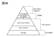
- FIG. 3B shows an example of a semiconductor device according to one embodiment of the present invention.
- FIG. 3B is a schematic diagram showing various memory devices used in the semiconductor device 10 and the semiconductor device 10A, arranged by hierarchy.
- L1 cache and L2 cache Multiple caches are provided, starting from the highest, in the order of L1 cache and L2 cache.
- Higher-level caches are required to operate faster, as they are accessed more frequently by the processor. Operating speed can also be increased by reducing the data capacity, so it is preferable to reduce the data capacity of higher-level caches.
- Higher-level caches are preferably located closer physically to the processor and have shorter wiring lengths, so they are preferably provided in a mixed-insertion configuration in the same layer as the processor.
- Lower-level caches may be provided in a different layer from the processor.
- the lowest level of cache can be called the LLC.
- an LLC is not required to operate faster than higher level caches, it is desirable for it to have a large storage capacity.
- the OS memory of one embodiment of the present invention described below has a fast operating speed and is capable of retaining data for a long period of time, making it suitable for use as an LLC.
- the LLC can also be called a Final Level cache (FLC).
- SRAM can be used for the various caches.
- OS memory can be suitably used for the LLC and main memory. This storage device has a fast operating speed and can retain data for long periods of time.
- layers 11 and 12 in FIG. 1A or 2A can be applied to the layer where the CPU/GPU is provided.
- Layer 13 can be applied to the layer where the LLC is provided,
- layer 14 can be applied to the layer where the main memory is provided, and
- layer 15 can be applied to the layer where the storage is provided.
- the configuration illustrated here does not use DRAM, which has traditionally been used as main memory, etc. Instead, DRAM is replaced with an OS memory according to one aspect of the present invention.
- This configuration makes it possible to dramatically reduce power consumption (for example, to 1/100 or 1/1000 or less), and it is expected that by deploying information processing devices including computers, servers, etc. to which this configuration is applied all over the world, it will be possible to make a significant contribution to curbing global warming.
- Table 1 shows the access time and capacity required for each memory. Note that Table 1 is a guideline and can be changed as appropriate according to the purpose of use, architecture, etc.
- access times and capacity vary depending on whether the storage device is a flash memory-based storage device such as an SSD (Solid State Drive) or SD card, or a hard disk.
- SSD Solid State Drive
- SD card Secure Digital Card
- Table 3 shows a comparison of conventional DRAM with examples of OS memory such as DOSRAM (Dynamic Oxide Semiconductor Random Access Memory) and NOSRAM. Note that DOSRAM has a configuration in which DRAM transistors are replaced with OS transistors.
- DOSRAM Dynamic Oxide Semiconductor Random Access Memory
- NOSRAM has the advantages over DRAM, such as the ability to perform non-destructive reads, the ability to have a cell area equivalent to that of DRAM, and low power consumption.
- Fig. 4A shows an example in which NOSRAM1 is used for the highest cache, NOSRAM2 for the lower cache, NOSRAM3 for the main memory, and a hard disk for storage.
- Fig. 4B shows an example in which 3D NAND memory is used for storage.
- Figure 4C shows an example in which NOSRAM2 is used as the main memory and NOSRAM3 is used as the storage.
- the NOSRAM1 is a memory capable of high-speed operation.
- a storage device equipped with the memory cells 20 illustrated above can be used.
- NOSRAM2 and NOSRAM3 are slower than NOSRAM1 in operating speed, they are memories with good data retention characteristics.
- a storage device equipped with the memory cells 30 exemplified above can be used.
- NOSRAM3 is a memory in which the memory cells 30 have a larger capacity than NOSRAM2, and thus has improved data retention characteristics.
- NOSRAM1 has the fastest operating speed, while NOSRAM3 has the slowest.
- NOSRAM3 has the longest data retention period, while NOSRAM1 has the shortest.
- NOSRAM1 has the shortest.
- NOSRAM1 which has the shortest data retention period, has a longer refresh cycle than a DRAM (e.g., about 60 ms).
- the data retention period is preferably 0.1 seconds or more, more preferably 1 second or more, and even more preferably 3 seconds or more.
- the data retention period is preferably 30 seconds or more, more preferably 1 minute or more, and even more preferably 10 minutes or more.
- the data retention period is preferably greater than 10 minutes, more preferably 1 hour or more, and even more preferably 1 day or more. Note that no upper limit is given for each data retention period, as the longer the better.
- NOSRAM3 For example, if the data retention period of NOSRAM3 is one year or more, it can be used as a substantially non-volatile memory, and can also be applied to storage. When used as storage, data can be rewritten once every few days.
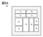
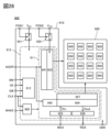
- Fig. 5A shows a block diagram of a processor as an example of the layer 12.
- Fig. 5A shows an example of the configuration of a CPU.
- Layer 12 shown in FIG. 5A has an ALU 71 (ALU: Arithmetic logic unit, arithmetic circuit), an ALU controller 72, an instruction decoder 73, an interrupt controller 74, a timing controller 75, a register 76, a register controller 77, a bus interface 78, a cache 79, and a cache interface 70.
- Layer 12 may also have a rewritable ROM and a ROM interface.
- the cache 79 and the cache interface 70 may be provided in different layers.
- the cache 79 is connected to the main memory provided in a different layer via the cache interface 70.
- the cache interface 70 has the function of supplying a portion of the data held in the main memory to the cache 79.
- the cache 79 has the function of holding that data.
- the arithmetic processing device shown in FIG. 5A is merely one example showing a simplified configuration, and actual arithmetic processing devices have a wide variety of configurations depending on their applications.
- the arithmetic processing device or configuration including the arithmetic circuit shown in FIG. 5A may be one core, and a configuration including multiple such cores with each core operating in parallel, in other words, a configuration similar to a GPU.
- the number of bits that the arithmetic processing device can handle in its internal arithmetic circuit or data bus can be, for example, 8 bits, 16 bits, 32 bits, 64 bits, etc.
- Instructions input to the processor via the bus interface 78 are input to the instruction decoder 73, decoded, and then input to the ALU controller 72, interrupt controller 74, register controller 77, and timing controller 75.
- the ALU controller 72, interrupt controller 74, register controller 77, and timing controller 75 perform various controls based on the decoded instructions. Specifically, the ALU controller 72 generates signals to control the operation of the ALU 71. Furthermore, while the arithmetic processing unit is executing a program, the interrupt controller 74 determines and processes interrupt requests from external input/output devices or peripheral circuits based on their priority or mask state. The register controller 77 generates the address of register 76, and reads or writes to register 76 depending on the state of the arithmetic processing unit.
- the timing controller 75 also generates signals that control the timing of the operations of the ALU 71, ALU controller 72, instruction decoder 73, interrupt controller 74, and register controller 77.
- the timing controller 75 includes an internal clock generating unit that generates an internal clock signal based on a reference clock signal, and supplies the internal clock signal to the various circuits described above.
- a memory device is provided for register 76 and cache 79. It is preferable to use SRAM for cache 79. Alternatively, NOSRAM may be used.
- the register controller 77 selects the holding operation in the register 76 according to instructions from the ALU 71. That is, it selects whether the memory cells in the register 76 will hold data using flip-flops or using capacitive elements. If holding data using flip-flops is selected, power supply voltage is supplied to the memory cells in the register 76. If holding data in capacitive elements is selected, data is rewritten to the capacitive elements, and the supply of power supply voltage to the memory cells in the register 76 can be stopped.
- FIG. 5B shows a block diagram of a GPU as an example of layer 11.
- the GPU shown in FIG. 5B has a controller 81, multiple processors 82, multiple caches 83, cache 84, an interface 85, etc.
- the controller 81 controls the processors 82, for example by allocating input commands to available processors 82.
- the processor 82 further includes a parallel computing unit capable of executing multiple processes simultaneously.
- the processor 82 includes, for example, multiple processor cores and registers.
- cache 83 Multiple caches 83 are provided for each processor 82. Furthermore, cache 84 can be shared by multiple processors 82.
- the controller 81 assigns and outputs the instruction to an available processor 82.
- the instruction may be divided into multiple threads and output to multiple processors 82.
- Data processed by the processor 82 is temporarily stored in a cache 83, cache 84, etc., and is sent to the CPU, etc. via an interface 85.
- the semiconductor device may be configured to have a processor such as a CPU and GPU, a DSP (Digital Signal Processor), an FPGA (Field-Programmable Gate Array), etc.
- a processor such as a CPU and GPU, a DSP (Digital Signal Processor), an FPGA (Field-Programmable Gate Array), etc.
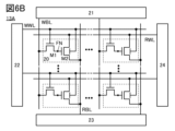
- FIG. 6A shows a memory array that may be used in layer 13 and its peripheral circuitry.
- Layer 13 has a plurality of memory cells 20 arranged in a matrix, and circuits 21, 22, 23, and 24.
- Circuit 21 is connected to a plurality of wirings WBL
- circuit 22 is connected to a plurality of wirings WWL
- circuit 23 is connected to a plurality of wirings RBL
- circuit 24 is connected to a plurality of wirings RWL.
- the wirings WWL and RWL extend in the row direction
- the wirings WBL and RBL extend in the column direction
- the wirings WWL and RWL intersect with the wirings WBL and RBL, respectively.
- Each of the memory cells 20 is connected to one each of the wirings WWL, WBL, RWL, and RBL.
- Memory cell 20 is composed of transistors M1 and M2.
- Transistor M1 has a gate connected to wiring WWL, one of its source and drain connected to wiring WBL, and the other connected to the gate of transistor M2.
- Transistor M2 has a source and drain connected to wiring RWL, and the other connected to wiring RBL.
- Node FN to which the other of the source and drain of transistor M1 and the gate of transistor M2 are connected, functions as a storage node for memory cell 20.
- Circuit 21, circuit 22, and circuit 24 function as driver circuits that supply signals to wiring WBL, wiring WWL, and wiring RWL, respectively.
- Circuit 23 functions as a read circuit and has a function of reading data stored in memory cell 20 by detecting the current flowing through wiring RBL or the potential of wiring RBL.
- both transistors M1 and M2 are N-channel transistors. If one or both of them are P-channel transistors, the potentials supplied to the various wirings can be changed appropriately.
- a lower potential e.g., a negative potential
- a lower potential may be applied to the wiring WWL of the non-selected row.
- the configuration shown in FIG. 6A is a configuration in which the memory cells 20 do not have capacitance, so there is little signal delay during writing and reading, making it possible to operate at high speed.
- Layer 13A shown in FIG. 6B is an example in which transistor M2 in memory cell 20 has a back gate (second gate).
- the back gate of transistor M2 is connected to wiring WWL. This allows transistor M2 in memory cell 20 to be reliably turned off by applying a low potential (e.g., negative potential) to the wiring WWL of an unselected row.
- a low potential e.g., negative potential
- the connection destination of the back gate of transistor M2 is not limited to this, and it may be configured to be connected to another wiring.
- the transistor M1 may have a backgate. In this case, it is preferable to apply a signal or potential that controls the threshold voltage of the transistor M1 to the backgate.
- the backgate may be connected to the wiring WWL, the wiring WBL, or the gate of the transistor M2.
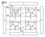
- FIG. 7A shows a memory array and its peripheral circuitry that may be used in layer 14.
- Layer 14 has a plurality of memory cells 30 arranged in a matrix, and circuits 31, 32, 33, and 34.
- Circuit 31 is connected to a plurality of wirings WBL
- circuit 32 is connected to a plurality of wirings WWL and a plurality of wirings CWL
- circuit 33 is connected to a plurality of wirings RBL
- circuit 34 is connected to a plurality of wirings RWL.
- Memory cell 30 is connected to one each of wirings WWL, wiring WBL, wiring RWL, wiring RBL, and wiring CWL.
- Memory cell 30 is composed of transistors M3 and M4, and a capacitor C.
- the gate of transistor M3 is connected to wiring WWL
- one of the source and drain is connected to wiring WBL
- the other is connected to the gate of transistor M4 and one electrode of capacitor C.
- the source and drain of transistor M2 is connected to wiring RWL, and the other is connected to wiring RBL.
- the other electrode of capacitor C is connected to wiring CWL.
- Node FN to which the other of the source and drain of transistor M3, the gate of transistor M4, and one electrode of capacitor C are connected, functions as a storage node for memory cell 30.
- Circuit 31, circuit 32, and circuit 34 function as driver circuits that supply signals to wiring WBL, wiring WWL, and wiring RWL, respectively.
- Circuit 32 also has a function of supplying signals to wiring CWL.
- Circuit 33 functions as a read circuit and has a function of detecting the current flowing through wiring RBL or the potential of wiring RBL.
- both transistors M3 and M4 are N-channel transistors. If one or both of them are P-channel transistors, the potentials supplied to the various wirings can be changed appropriately.
- the memory cell 30 has a capacitance C connected to the gate of the transistor M4, so the data retention period can be extended.
- Layer 14A shown in FIG. 7B is an example in which transistor M3 in memory cell 30 has a backgate.
- the backgate of transistor M3 is connected to wiring CWL.
- a low potential is applied to wiring CWL, which can shift the threshold voltage of transistor M3 in the positive direction and reduce the leakage current between the source and drain of transistor M3. This can further improve the data retention characteristics.
- FIG. 8A shows a schematic perspective view of a memory device that may be used for layer 15.
- the memory device is provided on an insulating layer 50 and has a plurality of memory strings 40.
- the memory strings 40 have a plurality of cell transistors stacked vertically on the upper surface of the insulating layer 50.
- the memory device further has a plurality of conductive layers 51, 52, 53, 54, and 55 that function as various wirings, and a plurality of plugs 56.
- FIG. 8A the orthogonal X, Y, and Z directions are indicated by arrows.
- the memory strings 40 are arranged at equal intervals in both the X and Y directions.
- FIG. 8A shows, as an example, one block having 5 x 5 memory strings 40.
- a memory device has multiple such blocks. In practice, it is preferable that one block has a larger number of memory strings 40.
- One memory string 40 is provided to connect between conductive layers 53 and 54.
- conductive layer 53 functions as a source line
- conductive layer 54 functions as a bit line.
- a plurality of conductive layers 51 are stacked between conductive layer 53 and conductive layer 54.
- Conductive layer 51 functions as a control gate line.
- a conductive layer 52 that functions as a selection line is provided between the uppermost conductive layer 51 and conductive layer 54.
- Each of the plurality of conductive layers 51 is connected to one of the plurality of conductive layers 55 via a plug 56.
- the conductive layers 54 and 52 extend in intersecting directions, forming a 5 x 5 matrix.
- the conductive layers 51 and 53 are connected to all memory strings 40 (here, 5 x 5) in the block.
- FIG. 8A shows an example of a configuration having five conductive layers 51
- the number of layers is not limited to this.
- the greater the number of stacked layers the greater the number of cell transistors that make up one memory string 40, and the greater the data capacity of the memory device.
- the more cell transistors that make up one memory string 40, the more preferable, and the number can be, for example, 64 or more, 128 or more, 160 or more, 192 or more, 224 or more, or 256 or more.
- FIG. 8B shows one memory string 40 and its surrounding configuration.
- a memory cell 65 that functions as a cell transistor is provided at the intersection of the memory string 40 and the conductive layer 51.
- the conductive layer 51 located at the bottom may function as a selection line.
- FIG. 8C is a circuit diagram of the configuration shown in FIG. 8B.
- Conductive layer 53 corresponds to wiring CL
- conductive layer 54 corresponds to wiring BL
- the lowest conductive layer 51 corresponds to wiring SSL
- the other conductive layers 51 correspond to wiring WL (wirings WL1 to WLm (m is an integer of 2 or more))
- conductive layer 52 corresponds to wiring BSL.
- a transistor STr As shown in FIG. 8C, a transistor STr, a plurality of transistors CTr, and a transistor BTr are provided between a wiring BL and a wiring CL.
- the transistors STr and BTr each function as a selection transistor, and the transistor CTr functions as a cell transistor.
- the transistor CTr functions as a memory element.
- the transistor CTr can be a memory element that uses a ferroelectric, such as a configuration in which a ferroelectric capacitor is connected to the gate or a configuration in which a ferroelectric is applied to the gate insulating layer.
- a charge trap type flash memory or a floating gate type flash memory can also be used.
- FIGS. 8D and 8E show an example in which one memory string 40 is composed of a pair of memory strings.
- conductive layer 53 functions as a pipe gate line
- conductive layer 57 functions as a source line.
- Transistor PTr provided at the bottom of the U-shaped memory string functions as a selection transistor (also called a pipe transistor) for connecting the pair of memory strings.
- the semiconductor device of one embodiment of the present invention can be applied to any communication device or information processing device that requires a processor, such as a mobile phone, a smartphone, a tablet terminal, a television device, a wearable device for VR (VR: Virtual Reality) or AR (AR: Augmented Reality), a wristwatch-type terminal, a game machine, a personal computer (including a notebook type), or a data server.
- the semiconductor device can be applied to any facility, device, or equipment that requires a processor, including moving objects such as automobiles, motorcycles, trains, airplanes, and drones, and even household appliances such as refrigerators and washing machines.
- This embodiment can be implemented by combining at least a portion of it with other embodiments described in this specification.
- a memory device has two vertical transistors, each having an oxide semiconductor layer in a channel formation region, stacked vertically.
- the gate of the lower vertical transistor is electrically connected to the source or drain of the upper vertical transistor.
- a capacitor is formed by the gate of the lower vertical transistor, the backgate of the upper vertical transistor, and an insulating layer between the gate and the backgate.
- the memory device of one embodiment of the present invention has a memory cell (hereinafter, referred to as a 2Tr1C memory cell) that is composed of two transistors and one capacitor.
- a 2Tr1C memory cell if a capacitor is provided in addition to the two transistors, there is a concern that the integration density of the memory cell will be reduced.
- By providing a capacitor so as to overlap with two vertical transistors in a plan view it is possible to prevent the area occupied by the memory cell from increasing due to the provision of the capacitor.
- 2Tr1C memory cells can be arranged at high density using a simple manufacturing method, and a memory device according to one embodiment of the present invention can have a large memory capacity.
- a transistor using an oxide semiconductor since a transistor using an oxide semiconductor has a small off-state current, when used in a memory device, stored content can be retained for a long period of time. In other words, a refresh operation is not required or is performed extremely infrequently, and therefore the power consumption of the memory device can be sufficiently reduced.
- the memory device By using a transistor using an oxide semiconductor in a memory device, the memory device can be highly integrated and have low power consumption.
- the on-state current of the transistor can be increased and the frequency characteristics can be improved. Therefore, reading and writing to the memory device can be performed faster.
- the source electrode and the drain electrode are located at different heights, and the current flowing through the semiconductor layer flows in the height direction.
- the transistor can also be called a VFET (Vertical Field Effect Transistor), a vertical transistor, a vertical channel transistor, a vertical channel transistor, or the like.
- vertical transistors can have a source electrode, semiconductor layer, and drain electrode stacked on top of each other, they can occupy a much smaller area than so-called planar transistors, which have semiconductor layers arranged in a flat plane.
- the channel length of a vertical transistor can be controlled by the thickness of the layers that are stacked. This makes it possible to realize a transistor with an extremely short channel length, which is difficult to achieve with a planar transistor. This makes it possible to realize a transistor that occupies a small area and has a large on-state current.
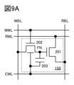
- ⁇ Configuration example 1 of storage device> 9A and 9B show an example of a circuit diagram of a memory cell 150.
- FIG. 9A and 9B show an example of a circuit diagram of a memory cell 150.
- the memory cell 150 shown in Figures 9A and 9B is composed of a transistor 201, a transistor 202, and a capacitor 203.
- the memory cell 150 is connected to one each of a wiring WWL, a wiring WBL, a wiring RWL, a wiring RBL, and a wiring CWL.
- the gate of the transistor 202 is connected to the wiring WWL, one of the source and drain is connected to the wiring WBL, the other is connected to the gate of the transistor 201 and one electrode of the capacitor 203, and the backgate is connected to the other electrode of the capacitor 203 and to the wiring CWL.
- the transistor 201 has one of the source and drain connected to the wiring RWL and the other connected to the wiring RBL.
- Transistor 202 preferably has a backgate.
- transistor 202 When transistor 202 is not selected, a low potential is applied to wiring CWL, which can shift the threshold voltage of transistor 202 in the positive direction and reduce leakage current between the source and drain of transistor 202. This can further improve data retention characteristics.
- transistor 201 may or may not have a backgate.
- FIG. 9A shows an example in which transistor 201 does not have a backgate
- FIG. 9B shows an example in which transistor 201 has a backgate.
- the memory cell 150 has a node FN to which the gate of the transistor 201, one of the source and drain of the transistor 202, and one electrode of the capacitor 203 are electrically connected.
- FIG. 9C shows an example of a plan view of one memory cell 150.
- FIG. 9D shows an example of a plan view of a plurality of memory cells 150 arranged in a matrix. Note that some elements are omitted from the plan view to clarify the drawing.
- FIG. 9D shows an example of 5 ⁇ 5 memory cells 150 arranged in the X and Y directions.
- the memory cell 150 is provided at the intersection of the conductive layer 265 extending in the X direction and the conductive layer 240 extending in the Y direction.
- the diameter of the opening shown by a solid circle in FIG.
- the memory cell 150 can be said to have a structure that allows for high integration and miniaturization.
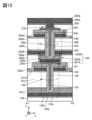
- FIG. 10 and 11 show an example of a cross-sectional view of a memory device having a memory cell 150.
- FIG. 10 is a cross-sectional view taken along dashed line A1-A2 in FIG. 9C.
- FIG. 11 is a cross-sectional view taken along dashed line A3-A4 in FIG. 9C.
- the memory device shown in Figures 10 and 11 has an insulating layer 140 on a substrate (not shown), a memory cell 150 on insulating layer 140, an insulating layer 161c on insulating layer 140, an insulating layer 161a on insulating layer 161c, an insulating layer 161d on insulating layer 161a, an insulating layer 185, an insulating layer 280a, an insulating layer 280f, an insulating layer 280b on insulating layer 280f, an insulating layer 280d on insulating layer 280b, an insulating layer 285, a conductive layer 265a on insulating layer 285, and a conductive layer 265b on conductive layer 265a.
- the insulating layer 140, the insulating layer 161a, the insulating layer 161c, the insulating layer 161d, the insulating layer 185, the insulating layer 280a, the insulating layer 280b, the insulating layer 280d, the insulating layer 280f, and the insulating layer 285 function as interlayer films. At least one of these interlayer films may be considered as a component of the memory cell 150.
- the conductive layer 265a and the conductive layer 265b function as wiring. At least one of the conductive layer 265a and the conductive layer 265b may be considered as a component of the memory cell 150.
- the conductive layer 265a and the conductive layer 265b may be collectively referred to as the conductive layer 265.
- Memory cell 150 has transistor 201A, transistor 202A, and capacitance element 203A.
- Transistor 201A has a conductive layer 120a, a conductive layer 120b on conductive layer 120a, a conductive layer 120c on conductive layer 120b, a conductive layer 145a on insulating layer 161d, a conductive layer 145b on conductive layer 145a, an oxide semiconductor layer 135, an insulating layer 151 on oxide semiconductor layer 135, and a conductive layer 164 on insulating layer 151.
- conductive layer 120a, conductive layer 120b, and conductive layer 120c may be collectively referred to as conductive layer 120.
- conductive layer 145a and conductive layer 145b may be collectively referred to as conductive layer 145.
- the oxide semiconductor layer 135 functions as a semiconductor layer
- the conductive layer 164 functions as a first gate electrode
- the insulating layer 151 functions as a first gate insulating layer
- the conductive layer 120 functions as one of the source electrode and the drain electrode
- the conductive layer 145 functions as the other of the source electrode and the drain electrode.
- the transistor 201A may further include a conductive layer that functions as a second gate electrode and an insulating layer that functions as a second gate insulating layer.
- the oxide semiconductor layer 135 has a region that overlaps with the conductive layer 164 via the insulating layer 151. At least a part of this region functions as a channel formation region of the transistor 201A.
- One of the region of the oxide semiconductor layer 135 that contacts the conductive layer 120 and the region of the oxide semiconductor layer 230 that contacts the conductive layer 145 functions as a source region, and the other functions as a drain region. In other words, the channel formation region is sandwiched between the source region and the drain region.
- Transistor 201A has a structure in which the oxide semiconductor layer 135 surrounds the conductive layer 164 that functions as a gate electrode, and therefore can be said to be a transistor with a CAA (Channel-All-Around) structure.
- Transistor 202A has conductive layer 220a, conductive layer 220b on conductive layer 220a, conductive layer 255 on insulating layer 280e, conductive layer 240a on insulating layer 280d, conductive layer 240b on conductive layer 240a, insulating layer 235a, insulating layer 235b, oxide semiconductor layer 230, insulating layer 250 on oxide semiconductor layer 230, and conductive layer 260 on insulating layer 250.
- Conductive layer 260 is electrically connected to conductive layer 265 that functions as a gate wiring.
- the conductive layers 220a and 220b may be collectively referred to as conductive layer 220.
- the conductive layers 240a and 240b may be collectively referred to as conductive layer 240.
- the insulating layers 235a and 235b may be collectively referred to as insulating layer 235.
- oxide semiconductor layer 230 functions as a semiconductor layer
- conductive layer 260 functions as a first gate electrode
- insulating layer 250 functions as a first gate insulating layer
- conductive layer 220 functions as one of the source electrode and drain electrode
- conductive layer 240 functions as the other of the source electrode and drain electrode
- conductive layer 255 functions as a second gate electrode
- insulating layer 235 functions as a second gate insulating layer.
- the conductive layer 260 functions as a gate electrode, and the conductive layer 255 functions as a back gate electrode.
- the conductive layer 260 which has a wider region facing the oxide semiconductor layer 230 than the conductive layer 255, as a gate, a gate electric field is applied to the oxide semiconductor layer 230 more efficiently, so that the electrical characteristics of the transistor can be improved in some cases.
- the insulating layer 250 functions as a gate insulating layer, and the insulating layer 235 functions as a back gate insulating layer.
- the conductive layer 260 may function as a back gate electrode, and the conductive layer 255 may function as a gate electrode.
- Transistor 202A When the channel length of a transistor becomes short, the transistor is likely to have normally-on characteristics due to the so-called short channel effect (SCE). Transistor 202A has a backgate. Therefore, by controlling the threshold voltage, it is easy to realize a transistor with normally-off characteristics. It is also possible to suppress fluctuations in the threshold voltage. In other words, even when miniaturized, transistor 202A has a high on-current, normally-off characteristics, and is highly reliable.
- the conductive layer 260 has a portion overlapping with the top surface of the conductive layer 240.
- a conductive layer 265 that functions as a gate wiring in addition to the conductive layer 260, and to provide an insulating layer 285 between the conductive layer 265 and the conductive layer 240.
- the conductive layer 265 is connected to the conductive layer 260 through an opening 270 provided in the insulating layer 285. This increases the physical distance between the conductive layer 265 and the conductive layer 240, and can reduce the parasitic capacitance generated between the gate wiring and the conductive layer 240. This can suppress a decrease in the frequency characteristics of the circuit using the transistor 202A.
- the conductive layer 260 does not extend in either the X or Y direction. It is preferable that the width of the conductive layer 260 is narrow in both the X and Y directions. This makes it possible to reduce the area of the region of the conductive layer 260 that overlaps with the upper surface of the conductive layer 240, and to reduce the parasitic capacitance that occurs between the conductive layer 260 and the conductive layer 240.
- the oxide semiconductor layer 230 has a region that overlaps with the conductive layer 255 via the insulating layer 235 and with the conductive layer 260 via the insulating layer 250. At least a part of the region functions as a channel formation region of the transistor 202A.
- One of the region of the oxide semiconductor layer 230 in contact with the conductive layer 220 and the region of the oxide semiconductor layer 230 in contact with the conductive layer 240 functions as a source region and the other functions as a drain region. In other words, the channel formation region is sandwiched between the source region and the drain region.
- the conductive layer 164 of the transistor 201A and the conductive layer 220 of the transistor 202A are each in contact with the conductive layer 165. That is, the conductive layer 164 and the conductive layer 220 are electrically connected through the conductive layer 165. As a result, the gate of the transistor 201A and the source or drain of the transistor 202A are electrically connected. Note that the conductive layer 165 may be considered as part of the source electrode or drain electrode of the transistor 202A.
- the conductive layer 164 does not extend in either the X direction or the Y direction. This makes it possible to reduce the area of the region of the conductive layer 164 that overlaps with the upper surface of the conductive layer 145, thereby reducing the parasitic capacitance that occurs between the conductive layer 164 and the conductive layer 145.
- the conductive layer 164, the conductive layer 165, the conductive layer 220a, and the conductive layer 220b function as one of the source electrode and drain electrode of the transistor 202A and as the gate electrode of the transistor 201A.
- the transistors 201A and 202A share part of the structure. With this structure, the transistors 201A and 202A can be provided without significantly increasing the occupied area in a planar view. As a result, the occupied area of the memory cell 150 can be reduced, and therefore the memory cells 150 can be arranged at a high density, thereby increasing the storage capacity of the storage device.
- the capacitor 203A has at least a conductive layer 220b, an insulating layer 280c on the conductive layer 220b, an insulating layer 280g on the insulating layer 280c, an insulating layer 280e on the insulating layer 280g, and a conductive layer 255 on the insulating layer 280e. At least some of the components of the capacitor 203A can also serve as components of the transistor 201A or the transistor 202A. Therefore, an increase in the number of manufacturing steps of the memory device due to the provision of the capacitor can be suppressed. By providing the capacitor 203A so as to overlap the transistors 201A and 202A in a plan view, a decrease in the integration density of the memory cell 150 can be suppressed.
- the shortest distance from the upper surface of conductive layer 220b to the lower surface of conductive layer 255 is preferably shorter than the shortest distance from the upper surface of conductive layer 255 to the lower surface of conductive layer 240. This allows the capacitance value of capacitance element 203A to be increased. In addition, the parasitic capacitance generated between conductive layer 240 and conductive layer 255 can be reduced.
- the memory cell 150 shown in FIG. 10 has a conductive layer 165, a conductive layer 220a, and a conductive layer 220b on an insulating layer 185.
- the conductive layer 165 is connected to the conductive layer 164 through an opening 174 provided in the insulating layer 185.
- the conductive layer 165, the conductive layer 220a, and the conductive layer 220b overlap with the top surface of the conductive layer 145 through the insulating layer 185.
- the capacitance element 203A it is preferable to increase the area of the region where the lower surface of the conductive layer 255 and the upper surface of the conductive layer 220b overlap.
- the area of the region where the lower surface of the conductive layer 255 and the upper surface of the conductive layer 220b overlap is increased, the area of the region where the lower surface of the conductive layer 220b and the upper surface of the conductive layer 145 overlap also increases.
- the physical distance between the conductive layer 165 and the conductive layer 145 is large, so that the parasitic capacitance generated between the conductive layer 165 and the conductive layer 145 can be reduced.
- the area of the region where the lower surface of the conductive layer 255 and the upper surface of the conductive layer 220b overlap and the area of the region where the lower surface of the conductive layer 220b and the upper surface of the conductive layer 145 overlap can each be increased, and the capacitance value of the capacitance element 203A can be increased.
- the capacitor 203A may have the insulating layer 280a between the insulating layer 280c and the insulating layer 280g.
- the insulating layer 280g, the insulating layer 280e, the conductive layer 255, and the like may be provided along the side and top surfaces of the conductive layer 220, similar to the insulating layer 280c. This can increase the area where the conductive layer 220b and the conductive layer 255 overlap with each other via the insulating layer, and increase the capacitance value of the capacitor 203A.
- insulating layer 280c, insulating layer 280g, insulating layer 280e, conductive layer 255, insulating layer 280f, insulating layer 280b, insulating layer 280d, conductive layer 240a, and conductive layer 240b have openings 290 that reach conductive layer 220.
- Conductive layer 220 has conductive layer 220a and conductive layer 220b on conductive layer 220a, and conductive layer 220b has a recess.
- conductive layer 220 has a recess, the bottom surface of which corresponds to the bottom surface of the recess in conductive layer 220b, and the side surface of which corresponds to the side surface of the recess in conductive layer 220b.
- conductive layer 220b has a first recess and a second recess located outside the first recess. The first recess is deeper than the second recess.
- a second recess is provided in conductive layer 220b, and then, when processing insulating layer 235, a first recess is provided in conductive layer 220b. Therefore, in FIG. 10 and the like, the side of the first recess is aligned with the surface of the insulating layer 235 facing the oxide semiconductor layer 230, and the side of the second recess is aligned with the side of the insulating layer 280c and the like facing the opening 290.
- the first recess and the second recess may be collectively referred to as recesses.
- the opening 290 overlaps with the recess of the conductive layer 220b.
- the sidewall of the opening 290 includes the side of the insulating layer 280c, the side of the insulating layer 280g, the side of the insulating layer 280e, the side of the conductive layer 255, the side of the insulating layer 280f, the side of the insulating layer 280b, the side of the insulating layer 280d, the side of the conductive layer 240a, and the side of the conductive layer 240b.
- the bottom of the opening 290 may be considered to include the bottom surface of the recess of the conductive layer 220b.
- the side of the recess of the conductive layer 220b may be considered to be part of the sidewall of the opening 290. In other words, the recess of the conductive layer 220b may be considered to be part of the opening 290.
- the openings 290 include an opening in insulating layer 280c, an opening in insulating layer 280g, an opening in insulating layer 280e, an opening in conductive layer 255, an opening in insulating layer 280f, an opening in insulating layer 280b, an opening in insulating layer 280d, an opening in conductive layer 240a, and an opening in conductive layer 240b.
- an opening in the region where the insulating layer 280c overlaps with the conductive layer 220a is a part of the opening 290
- an opening in the region where the insulating layer 280g overlaps with the conductive layer 220a is another part of the opening 290
- an opening in the region where the insulating layer 280e overlaps with the conductive layer 220a is another part of the opening 290
- an opening in the region where the conductive layer 255 overlaps with the conductive layer 220a is another part of the opening 290
- an opening in the region where the insulating layer 280f overlaps with the conductive layer 220a is another part of the opening 290.
- the opening in the region where the insulating layer 280b overlaps with the conductive layer 220a is another part of the opening 290
- the opening in the region where the insulating layer 280d overlaps with the conductive layer 220a is another part of the opening 290
- the opening in the region where the conductive layer 240a overlaps with the conductive layer 220a is another part of the opening 290
- the opening in the region where the conductive layer 240b overlaps with the conductive layer 220a is another part of the opening 290.
- the shape and size of the opening 290 in a plan view may differ depending on each layer. Also, when the top surface shape of the opening 290 is circular, the openings in each layer may be concentric or not concentric.
- the opening in the insulating layer 280a may also be considered as part of the opening 290.
- At least some of the components of transistor 202A are disposed within opening 290. Specifically, insulating layer 235, oxide semiconductor layer 230, insulating layer 250, and conductive layer 260 are disposed such that at least a portion of each of them is located within opening 290.
- the insulating layer 235 has at least a region located between the oxide semiconductor layer 230 and the conductive layer 255.
- the oxide semiconductor layer 230 contacts the insulating layer 235 within the opening 290.
- the insulating layer 235 contacts the bottom and side of the recess (specifically, the second recess) of the conductive layer 220, and also contacts the side of the insulating layer 280c, the side of the insulating layer 280g, the side of the insulating layer 280e, the side of the conductive layer 255, the side of the insulating layer 280f, the side of the insulating layer 280b, the side of the insulating layer 280d, the side of the conductive layer 240a, and the side of the conductive layer 240b in the opening 290.
- the oxide semiconductor layer 230 contacts the bottom and side of the recess (specifically, the first recess) of the conductive layer 220, the insulating layer 235, and the upper surface of the conductive layer 240b.
- the insulating layer 250 is located inside the oxide semiconductor layer 230 in the opening 290, and the conductive layer 260 is located inside the insulating layer 250 in the opening 290.
- the insulating layer 235 is provided along at least a portion of the sidewall of the opening 290.
- the portions of the oxide semiconductor layer 230 and the insulating layer 250 that are disposed within the opening 290 are provided to reflect the shape of the opening 290.
- the oxide semiconductor layer 230 is provided to cover the bottom surface of the recess in the conductive layer 220b and the insulating layer 235, and the insulating layer 250 is provided to cover the oxide semiconductor layer 230.
- the conductive layer 260 is then provided to fill at least a portion of the recess in the insulating layer 250 that reflects the shape of the opening 290.
- Insulating layer 235 is formed, for example, by forming an insulating film so as to cover opening 290, and processing the insulating film by anisotropic etching to remove the region of the insulating film located on the upper surface of conductive layer 240b and the region located on the bottom surface of opening 290. This allows insulating layer 235 to remain only on the side surfaces within opening 290.
- the insulating film that becomes insulating layer 235 is preferably processed by performing highly anisotropic etching using a dry etching method.
- the insulating layer 235 may have a single-layer structure or a laminated structure. In this embodiment, an example in which the insulating layer 235 has an insulating layer 235a and an insulating layer 235b on the insulating layer 235a is mainly shown.
- the insulating layer 235a and the insulating layer 235b function as a second gate insulating layer (also called a back-gate insulating layer) of the transistor 202A.
- one of the insulating layers 235a and 235b has an insulating layer that has a region that contains oxygen that is desorbed by heating. It is also preferable that the other of the insulating layers 235a and 235b has a barrier insulating layer against hydrogen.
- a silicon nitride film for the insulating layer 235a and a silicon oxide film for the insulating layer 235b it is preferable to use a silicon oxide film for the insulating layer 235a and a silicon nitride film for the insulating layer 235b.
- a low-k material particularly an inorganic material with a low dielectric constant, may be used for the layer constituting the insulating layer 235.
- an inorganic insulating material such as silicon oxide, silicon oxynitride, or silicon nitride oxide may be used.
- TEOS Tetra- Ethyl -Ortho-Silicate, chemical formula: Si( OC2H5 ) 4 ) may also be used.
- an insulating layer 235a is provided in contact with the bottom and side surfaces of the recess of the conductive layer 220b, and an insulating layer 235b is provided on the insulating layer 235a.
- an insulating film that will become the insulating layer 235a and an insulating film that will become the insulating layer 235b are stacked, and then the two insulating films are processed to form the insulating layer 235a and the insulating layer 235b of the structure shown in FIG. 10. Therefore, it can be said that this structure can be manufactured relatively easily.
- transistor 202A At least one layer constituting conductive layer 260 is provided within opening 290. If conductive layer 260 has a laminated structure, as transistor 202A is miniaturized and the diameter of opening 290 becomes smaller, it becomes more difficult to arrange all layers constituting conductive layer 260 in opening 290.
- the height of the bottom surface of the insulating layer 250 and the height of the bottom surface of the conductive layer 260 in the opening 290 can be lower than the height of the top surface of the conductive layer 220b that contacts the insulating layer 280c with respect to the top surface of the insulating layer 140 as compared to a case where the recess is not provided.
- the gate electric field is also easier to apply to the region of the oxide semiconductor layer 230 that contacts the conductive layer 220b, the on-current of the transistor 202A can be increased.
- the conductive layer 220 or the conductive layer 240 is used as the drain electrode, the electrical characteristics of the transistor 202A can be improved.
- the height of each surface can be determined based on the surface on which the memory cell or transistor is formed.
- the top surface of the insulating layer 140 is used as the reference.
- the surface used as the reference is not limited to the surface on which the memory cell or transistor is formed.
- the top surface of the substrate on which the transistor, memory cell, or memory device is provided may be used as the reference.
- the oxide semiconductor layer 230 contacts the bottom and side surfaces of the recess in the conductive layer 220b, and the top surface of the conductive layer 240b.
- the conductive layer 220b has a recess, which increases the area of contact between the oxide semiconductor layer 230 and the conductive layer 220b. This reduces the contact resistance between the oxide semiconductor layer 230 and the conductive layer 220b. This suppresses a decrease in the on-current of the transistor 202A caused by the contact resistance between the conductive layer 220 and the oxide semiconductor layer 230.
- a conductive material containing oxygen for the conductive layer 220b. This can reduce the contact resistance between the oxide semiconductor layer 230 and the conductive layer 220b.
- the conductive layer 220 and the conductive layer 240 have a stacked structure
- a conductive material containing oxygen is used for the layer of the stacked structure closest to the channel formation region, and the contact resistance with the oxide semiconductor layer 230 is reduced, thereby shortening the current path between the source and drain, and increasing the on-current of the transistor. For this reason, it is preferable to use a conductive material containing oxygen for the conductive layer 220b and the conductive layer 240a, for example.
- a metal oxide having electrical conductivity also called an oxide conductor
- the conductive layer 240 has a two-layer structure of a conductive layer 240a and a conductive layer 240b on the conductive layer 240a.
- a conductive material containing oxygen as the conductive layer 240b
- a material having a higher conductivity than the conductive layer 240b as the conductive layer 240a.
- an oxide conductor for example, ITO, ITSO, or IZO (registered trademark)
- tungsten as the conductive layer 240a.
- Ruthenium, titanium nitride, tantalum nitride, or the like may also be used as the conductive layer 240a.
- the layer of the conductive layer 240 that is mainly in contact with the oxide semiconductor layer 230 is the conductive layer 240b.
- the contact resistance with the oxide semiconductor layer 230 can be reduced, which is preferable.
- the conductivity of the conductive layer 240 can be increased, which is preferable.
- a conductive material containing oxygen can be used as the conductive layer 240a, and a material having a higher conductivity than the conductive layer 240a can be used as the conductive layer 240b.
- an oxide conductor is used for the layer of the conductive layer 240 that is closest to the channel formation region of the oxide semiconductor layer 230. This makes it possible to shorten the current path between the source and drain, and increase the on-current of the transistor.
- a conductive material that is not easily oxidized or a conductive material that has a function of suppressing the diffusion of oxygen as the conductive layer 165, a material with high conductivity as the conductive layer 220a, and a conductive material containing oxygen (more preferably an oxide conductor) as the conductive layer 220b.
- a conductive material containing oxygen more preferably an oxide conductor
- titanium nitride as the conductive layer 165, tungsten as the conductive layer 220a, and an oxide conductor (for example, ITO, ITSO, or IZO (registered trademark)) as the conductive layer 220b.
- titanium nitride contacts the insulating layer 185, and the oxide conductor contacts the oxide semiconductor layer 230.
- an oxide conductor is used in the layer closest to the channel formation region of the oxide semiconductor layer 230. Compared to tungsten, the oxide conductor has a lower contact resistance with the oxide semiconductor layer 230, so that the current path between the source and drain can be shortened and the on-current of the transistor 202A can be increased. With this structure, the conductive layer 220 can maintain conductivity even when in contact with the oxide semiconductor layer 230. In addition, when an oxide insulating layer is used for the insulating layer 185, the insulating layer 185 can prevent the conductive layer 220 from being excessively oxidized. In addition, by using a metal material (here, tungsten) having higher conductivity than an oxide conductor and titanium nitride as the conductive layer 220a, the conductivity of the conductive layer 220 can be increased.
- a metal material here, tungsten
- the conductive layer 265 preferably has high conductivity because it functions as a gate wiring.
- FIG. 10 and other figures show an example in which the conductive layer 265 has a two-layer structure of a conductive layer 265a and a conductive layer 265b on the conductive layer 265a.
- tantalum nitride as the conductive layer 265a and copper as the conductive layer 265b. With such a structure, the conductivity of the conductive layer 265 can be increased.
- the conductive layer 265 may also have a laminated structure of three or more layers.
- the conductive layer 265 may have a three-layer structure of tantalum nitride, titanium nitride on the tantalum nitride, and tungsten on the titanium nitride.
- any of the end of the oxide semiconductor layer 230, the end of the conductive layer 240a, and the end of the conductive layer 240b may be located inside or outside the other. Note that the same can be said about the conductive layer 145 and the oxide semiconductor layer 135.
- the side of insulating layer 280c, the side of insulating layer 280g, the side of insulating layer 280e, the side of conductive layer 255, the side of insulating layer 280f, the side of insulating layer 280b, the side of insulating layer 280d, the side of conductive layer 240a, and the side of conductive layer 240b are aligned within opening 290, the film thickness distribution of insulating layer 235, oxide semiconductor layer 230, etc. provided inside opening 290 can be made uniform. In addition, it is possible to prevent insulating layer 235, oxide semiconductor layer 230, etc. from being divided by steps generated on the sidewall of opening 290.
- the present invention is not limited to this.
- the side surface of the conductive layer 240 in the opening 290 and the side surface of the insulating layer 280d in the opening 290 may be discontinuous.
- the inclination of the side surface of the conductive layer 240 in the opening 290 and the inclination of the side surface of the insulating layer 280d in the opening 290 may differ from each other.
- the taper angle of the side surface of the conductive layer 240 in the opening 290 is smaller than the taper angle of the side surface of the insulating layer 280d in the opening 290.
- the coverage of the oxide semiconductor layer 230 on the side surface of the conductive layer 240 in the opening 290 is improved, and defects such as voids can be reduced.
- the inclination of the side surface of each layer in the opening 290 may be different for the insulating layers 280b to 280g.
- the inclination of the side surface of each layer in the opening 290 may be different.
- insulating layer 161c, insulating layer 161a, insulating layer 161d, conductive layer 145a, and conductive layer 145b have openings 190 that reach conductive layer 120.
- opening 190 and each layer in which opening 190 is provided the above-mentioned description of opening 290 and each layer in which opening 290 is provided can also be referred to.
- the conductive layer 120 has a conductive layer 120a, a conductive layer 120b on the conductive layer 120a, and a conductive layer 120c on the conductive layer 120b, and a recess is provided in the conductive layer 120c.
- the opening 190 overlaps with the recess of the conductive layer 120c.
- the shape and size of the opening 190 in a plan view may differ depending on each layer. Furthermore, when the top surface shape of the opening 190 is circular, the openings in each layer may or may not be concentric.
- oxide semiconductor layer 135, insulating layer 151, and conductive layer 164 are disposed such that at least a portion of each of them is located within opening 190.
- the oxide semiconductor layer 135 contacts the bottom and side surfaces of the recess of the conductive layer 220, and also contacts the side surfaces of the insulating layer 161c, the side surfaces of the insulating layer 161a, the side surfaces of the insulating layer 161d, the side surfaces of the conductive layer 145a, and the side surfaces of the conductive layer 145b within the opening 190.
- the insulating layer 151 is located inside the oxide semiconductor layer 135 within the opening 190
- the conductive layer 164 is located inside the insulating layer 151 within the opening 190.
- oxide semiconductor layer 135 and the like provided inside opening 190 can be made uniform.
- oxide semiconductor layer 135 and the like can be divided by steps or the like that occur on the side walls of opening 190.
- the oxide semiconductor layer 135 is provided along the sidewall of the opening 190. Furthermore, the portions of the oxide semiconductor layer 135 and the insulating layer 151 that are disposed within the opening 190 are provided to reflect the shape of the opening 190. Then, the conductive layer 164 is provided so as to fill at least a portion of the recess in the insulating layer 151 that reflects the shape of the opening 190.
- transistor 201A At least one layer constituting conductive layer 164 is provided within opening 190. If conductive layer 164 has a stacked structure, as transistor 201A is miniaturized and the diameter of opening 190 becomes smaller, it becomes more difficult to arrange all layers constituting conductive layer 164 in opening 190.
- transistor 201A Similar to transistor 202A, by having a recess in the position where conductive layer 120c overlaps with opening 190, a gate electric field is more easily applied to the channel formation region of oxide semiconductor layer 135 than when the recess is not present, and the electrical characteristics of transistor 201A can be improved. Furthermore, since a gate electric field is more easily applied to the region of oxide semiconductor layer 135 that is in contact with conductive layer 120c, the on-current of transistor 201A can be increased. Moreover, whether conductive layer 120 or conductive layer 145 is used for the drain electrode, the electrical characteristics of transistor 201A can be improved.
- the oxide semiconductor layer 135 contacts the bottom and side surfaces of the recess in the conductive layer 120c, and the top surface of the conductive layer 145b.
- the conductive layer 120c has a recess, which increases the area over which the oxide semiconductor layer 135 contacts the conductive layer 120c. This reduces the contact resistance between the oxide semiconductor layer 135 and the conductive layer 120c. This prevents a decrease in the on-current of the transistor 201A due to the contact resistance between the conductive layer 120 and the oxide semiconductor layer 135.
- conductive layer 145a it is preferable to use a material suitable for conductive layer 240a.
- conductive layer 145b it is preferable to use a material suitable for conductive layer 240b.
- the transistor 201A it is preferable to apply a suitable configuration to the three-layer structure of the conductive layers 120a to 120c described above, which is the three-layer structure of the conductive layers 165, the conductive layer 220a, and the conductive layer 220b.
- the transistor 201A the current path between the source and drain can be shortened, and the on-current can be increased.
- the insulating layer 140 can suppress excessive oxidation of the conductive layer 120.
- the conductivity of the conductive layer 120 can be increased.
- Transistor 201A and transistor 202A each have a metal oxide (also called an oxide semiconductor) that functions as a semiconductor in an oxide semiconductor layer (oxide semiconductor layer 135 or oxide semiconductor layer 230) that includes a channel formation region.
- transistor 201A and transistor 202A can each be considered an OS transistor.
- oxygen vacancies ( VO ) and impurities are present in a channel formation region in an oxide semiconductor, the electrical characteristics of an OS transistor are likely to fluctuate and the reliability may be reduced. Furthermore, hydrogen near the oxygen vacancies may form a defect in which hydrogen is inserted into the oxygen vacancies (hereinafter sometimes referred to as VOH ), and may generate electrons that serve as carriers. For this reason, when oxygen vacancies are present in the channel formation region in the oxide semiconductor, the OS transistor is likely to have normally-on characteristics. Therefore, it is preferable that oxygen vacancies and impurities are reduced as much as possible in the channel formation region in the oxide semiconductor. In other words, it is preferable that the carrier concentration of the channel formation region in the oxide semiconductor is reduced and the channel formation region in the oxide semiconductor is made i-type (intrinsic) or substantially i-type.
- the source and drain regions of an OS transistor are preferably regions having more oxygen vacancies, more VOH , or a higher concentration of impurities such as hydrogen, nitrogen, or metal elements than the channel formation region, thereby increasing the carrier concentration and lowering the resistance. That is, the source and drain regions of an OS transistor are preferably n-type regions having a higher carrier concentration and lower resistance than the channel formation region.
- the oxide semiconductor layer 230 is provided inside the opening 290.
- the transistor 202A has one of the source electrode and drain electrode (conductive layer 220 in this case) located on the bottom and the other of the source electrode and drain electrode (conductive layer 240 in this case) located on the top, so that the current flows in the vertical direction. In other words, a channel is formed along the side surface of the opening 290.
- the conductive layer 255 surrounds the entire outer periphery of the oxide semiconductor layer 230 via the insulating layer 235.
- the oxide semiconductor layer 230 also surrounds the entire outer periphery of the conductive layer 260 located in the opening 290 via the insulating layer 250.
- the channel formation region of the transistor 202A can be formed on the entire outer surface of the oxide semiconductor layer 230 in the opening 290 (the entire region in contact with the insulating layer 235). In this case, for example, the length of the outer periphery of the oxide semiconductor layer 230 determines the channel width of the transistor 202A.
- the channel width of the transistor 202A is determined by the width of the opening 290 (the diameter when the opening 290 is circular in a plan view).
- the width of the opening 290 By increasing the width of the opening 290, the channel width per unit area can be increased, and the on-current can be increased.
- the width of the opening 290 may vary in the depth direction.
- the shortest distance between the two side surfaces of the conductive layer 255 on the opening 290 side in a cross-sectional view is used as the width.
- the minimum value of the width of the opening 290 in the conductive layer 255 is used as the width of the opening 290.
- the width of the opening 290 at the highest position in the conductive layer 255, the width of the opening 290 at the lowest position, the width of the opening 290 at the midpoint between these, or the average value of these three widths may be used as the width of the opening 290.
- the method of determining the width of the opening 290 is not particularly limited.
- the shortest distance between the two side surfaces on the opening 290 side of any layer in which the opening 290 is provided may be used as the width of the opening 290.
- the width of the opening 290 at the highest position in any layer in which the opening 290 is provided, the width of the opening 290 at the lowest position, the width of the opening 290 at the midpoint between these, or the average value of these three widths may be used as the width of the opening 290.
- the width of the opening 290 is limited by the exposure limit of photolithography.
- the width of the opening 290 is set by the film thickness of each of the insulating layer 235, the oxide semiconductor layer 230, the insulating layer 250, and the conductive layer 260 provided in the opening 290.
- the width of the opening 290 is, for example, 5 nm or more, 10 nm or more, or 20 nm or more, and is preferably 100 nm or less, 60 nm or less, 50 nm or less, 40 nm or less, or 30 nm or less.
- the width D of the opening 290 corresponds to the diameter of the opening 290, and the channel width W can be calculated as "D x ⁇ ".
- the channel length L of the transistor 202A is at least smaller than the channel width W of the transistor 202A.
- the channel length L of the transistor 202A is preferably 0.1 to 0.99 times the channel width W of the transistor 202A, and more preferably 0.5 to 0.8 times. With such a configuration, a transistor having good electrical characteristics and high reliability can be realized.
- the insulating layer 235, the oxide semiconductor layer 230, the insulating layer 250, and the conductive layer 260 are arranged concentrically.
- the distance between the conductive layer 255 and the oxide semiconductor layer 230, and the distance between the conductive layer 260 and the oxide semiconductor layer 230 are each approximately uniform, so that a gate electric field can be applied to the oxide semiconductor layer 230 approximately uniformly.
- the opening 290 can be, for example, a circle, an approximately circular shape such as an ellipse, a polygon such as a triangle, a quadrangle (including a rectangle, a diamond, and a square), a pentagon, or a star-shaped polygon, or a shape with rounded corners of these polygons.
- the polygon may be either a concave polygon (a polygon with at least one interior angle exceeding 180 degrees) or a convex polygon (a polygon with all interior angles less than 180 degrees). As shown in FIG.
- the opening 290 is preferably circular. By making it circular, the processing accuracy when forming the opening can be improved, and an opening of a fine size can be formed.
- a circle is not limited to a perfect circle.
- the channel length of transistor 202A can be considered to be the distance between the source region and the drain region.
- the channel length of transistor 202A can be determined by the thicknesses of insulating layer 280c, insulating layer 280g, insulating layer 280e, conductive layer 255, insulating layer 280f, insulating layer 280b, insulating layer 280d, etc. on conductive layer 220.
- the threshold voltage of the transistor 202A can be controlled by the potential applied to the conductive layer 255.
- the portion of the oxide semiconductor layer 230 that overlaps with the conductive layer 255 via the insulating layer 235 is most susceptible to the influence of the conductive layer 255.
- At least the region of the oxide semiconductor layer 230 that overlaps with the conductive layer 255 via the insulating layer 235 and overlaps with the conductive layer 265a via the insulating layer 250 can be called a channel formation region.
- the channel formation region is preferably controlled to have high resistance by the potential applied to the conductive layer 255.
- the region of the oxide semiconductor layer 230 that contacts the conductive layer 240b or the conductive layer 220b and its vicinity can be called the source region or drain region.
- the source region and the drain region are n-type regions (low resistance regions) that have a higher carrier concentration than the channel formation region.
- the channel length is limited by the exposure limit of photolithography, but in one aspect of the present invention, the channel length can be set by the film thickness of a portion of the layer in which the opening 290 is provided. Therefore, the channel length of the transistor 202A can be made to be an extremely fine structure that is below the exposure limit of photolithography (for example, 60 nm or less, 50 nm or less, 40 nm or less, 30 nm or less, 20 nm or less, or 10 nm or less, and 0.1 nm or more, 1 nm or more, or 5 nm or more). This increases the on-current of the transistor 202A, and improves the frequency characteristics.
- the exposure limit of photolithography for example, 60 nm or less, 50 nm or less, 40 nm or less, 30 nm or less, 20 nm or less, or 10 nm or less, and 0.1 nm or more, 1 nm or more, or 5 nm or more.
- a channel formation region, a source region, and a drain region can be formed within the opening 290.
- the channel width of transistor 201A is determined by the width of opening 190.
- the width of opening 190 is set by the film thickness of oxide semiconductor layer 135, insulating layer 151, and conductive layer 164 provided in opening 190.
- the channel length of transistor 201A is determined by the thickness of insulating layer 161c, insulating layer 161a, insulating layer 161d, etc. on conductive layer 120c.
- Memory cell 150 shown in FIG. 12 differs from memory cell 150 shown in FIG. 10 in that it does not have transistor 201A but has transistor 201B.
- Transistor 201B differs from transistor 201A in that it has an insulating layer 131.
- the transistor 202A has an insulating layer 235 that functions as a back-gate insulating layer.
- the transistor 201B shown in FIG. 12 is a transistor that does not have a back-gate, but may have a layer corresponding to the insulating layer 235. That is, the insulating layer 131 may be provided on the side wall of the opening 190 using the same material and manufacturing method as the insulating layer 235. When the insulating layer 131 is not provided, the oxide semiconductor layer 135 is in contact with the insulating layer 161a, the insulating layer 161c, and the insulating layer 161d inside the opening 190.
- the insulating layer that the oxide semiconductor layer 135 is in contact with inside the opening 190 is only the insulating layer 131.
- the insulating layer 131 it is possible to supply oxygen to the oxide semiconductor layer 135, suppress diffusion of hydrogen into the oxide semiconductor layer 135, control the channel length, and the like.
- Memory cell 150 shown in FIG. 13 differs from memory cell 150 shown in FIG. 10 in that it does not have transistor 201A but has transistor 201C.
- Transistor 201C differs from transistor 201A in that it has a conductive layer 155 and an insulating layer 131.
- transistor 201C In transistor 201C, conductive layer 155 functions as a second gate electrode, and insulating layer 131 functions as a second gate insulating layer.
- the conductive layer 164 functions as a gate electrode and the conductive layer 155 functions as a back gate electrode.
- the gate electric field is applied to the oxide semiconductor layer 135 more efficiently, which may improve the electrical characteristics of the transistor 201C.
- the insulating layer 151 functions as a gate insulating layer and the insulating layer 131 functions as a back gate insulating layer.
- the conductive layer 164 may function as a back gate electrode and the conductive layer 155 may function as a gate electrode.
- An insulating layer 161e is provided on the insulating layer 161a, a conductive layer 155 is provided on the insulating layer 161e, an insulating layer 161f is provided so as to cover the top and side surfaces of the conductive layer 155, and an insulating layer 161b is provided on the insulating layer 161f.
- An opening 190 is provided in the insulating layer 161e, the insulating layer 161f, and the conductive layer 155.
- An insulating layer 131 is provided along the sidewall of the opening 190, and an oxide semiconductor layer 135 is provided so as to be in contact with the insulating layer 131.
- the circuit diagram of the memory cell 150 shown in FIG. 13 corresponds to FIG. 9B.
- the shortest distance from the upper surface of conductive layer 220b to the lower surface of conductive layer 255 is preferably shorter than the shortest distance from the upper surface of conductive layer 155 to the lower surface of conductive layer 145.
- the shortest distance from the upper surface of conductive layer 220b to the lower surface of conductive layer 255 is preferably shorter than the shortest distance from the upper surface of conductive layer 120 to the lower surface of conductive layer 155. This makes it possible to increase the capacitance value of capacitance element 203A.
- the memory cell 150 shown in FIG. 14 differs from the memory cell 150 shown in FIG. 10 in that it does not have a transistor 202A and a capacitor 203A, but has a transistor 202B and a capacitor 203B.
- the only layer between the conductive layer 220b and the conductive layer 255 is the insulating layer 280g.
- the capacitance value of the capacitor 203B can be increased, which is preferable.
- problems such as leakage currents in the transistor and the capacitor may occur due to the thinning of the dielectric used in the capacitor.
- it may be preferable to have not only the insulating layer 280g but also one or both of the insulating layer 280c and the insulating layer 280a between the conductive layer 220b and the conductive layer 255.
- the insulating layer 280g but also one or both of the insulating layer 280c and the insulating layer 280a, it may be possible to further suppress impurities from being mixed into the oxide semiconductor layer 230 and the amount of oxygen in the oxide semiconductor layer 230 from becoming insufficient or excessive.
- the memory cell 150 shown in FIG. 15 differs from the memory cell 150 shown in FIG. 14 in that it does not have a conductive layer 165 and an insulating layer 185.
- the memory cell 150 shown in FIG. 15 does not have a conductive layer 165 and an insulating layer 185, and therefore the number of manufacturing steps can be reduced compared to the memory cell 150 shown in FIG. 14, which is preferable.
- FIG. 15 shows an example in which the ends of conductive layer 164, conductive layer 220a, and conductive layer 220b are aligned.
- a conductive film that will become conductive layer 164, a conductive film that will become conductive layer 220a, and a conductive film that will become conductive layer 220b are formed in this order, and these three conductive films are processed using the same mask, thereby forming conductive layer 164, conductive layer 220a, and conductive layer 220b shown in FIG. 15.
- the transistors 201A and 202B share part of the structure. With this configuration, the transistors 201A and 202B can be provided without significantly increasing the occupied area in a planar view. This reduces the occupied area of the memory cells 150, and therefore the memory cells 150 can be arranged at a high density, thereby increasing the memory capacity of the memory device. In other words, the memory device can be highly integrated.
- Memory cell 150 shown in FIG. 16 differs from memory cell 150 shown in FIG. 15 in that it does not have transistor 202B but has transistor 202C.
- Transistor 202C differs from transistor 202B primarily in that conductive layer 220b has only one recess.
- a recess may be formed in the conductive layer 220b in one or both of the steps of forming the opening 290 and the step of forming the insulating layer 235.
- Transistor 202B shows an example in which a recess is formed in the conductive layer 220b in both steps
- transistor 202C shows an example in which a recess is not formed in the conductive layer 220b in the step of forming the opening 290, but is formed in the step of forming the insulating layer 235.
- insulating layer 235 contacts the side of insulating layer 280g, the side of conductive layer 255, the side of insulating layer 280f, the side of insulating layer 280b, the side of insulating layer 280d, the side of conductive layer 240, and the top surface of conductive layer 220b within opening 290.
- oxide semiconductor layer 230 contacts the bottom and side of the recess of conductive layer 220b.
- the height of the bottom surface of the conductive layer 260 within the opening 290 can be reduced, making it easier for a gate electric field to be applied to the channel formation region of the oxide semiconductor layer 230, thereby improving the electrical characteristics of the transistor 202A.
- the oxide semiconductor layer 230 can contact the bottom and side surfaces of the recess in the conductive layer 220b, increasing the contact area between the oxide semiconductor layer 230 and the conductive layer 220b, which is preferable because it reduces the contact resistance between the oxide semiconductor layer 230 and the conductive layer 220.
- Figs. 17A to 17C show examples of plan views of the capacitive element 203.
- FIG. 17A shows an example in which the center of the conductive layer 220, the center of the opening 190 and the opening 290, and the center of the region where the conductive layer 255 and the conductive layer 145 intersect (also called the intersection) all coincide (i.e., are at the same position) in a plan view.
- the capacitor 203 can be provided without increasing the area occupied by the memory cell having the transistor 201 and the transistor 202 in a plan view, which is preferable.
- plan view of the capacitive element 203B in the memory cell 150 shown in Figures 10 to 16 corresponds to Figure 17A.
- the center of the conductive layer 220 may be located at a position different from one or both of the centers of the openings 190 and 290.
- the center of the conductive layer 220 may also be located at a position different from the center of the intersection of the conductive layers 255 and 145. Therefore, it is possible to reduce the manufacturing cost of the memory cells 150 and suppress a decrease in yield, to the extent that the integration level is not significantly reduced.
- FIG. 17B shows an example in which, in a plan view, the centers of openings 190 and 290 and the center of the intersection between conductive layer 255 and conductive layer 145 are in the same position, and the center of conductive layer 220 is in a different position.
- plan view of the capacitive element 203C in the memory cell 150 shown in FIG. 18 corresponds to FIG. 17B.
- Capacitive element 203C shown in FIG. 18 has a structure in which conductive layer 220b, insulating layer 280g, and conductive layer 255 are stacked in this order.
- the region of capacitive element 203C located to the right of conductive layer 260 is larger than the region located to the left.
- the structure shown in FIG. 17B can be intentionally fabricated, or the structure shown in FIG. 17B can be fabricated as a result of misalignment during the process of fabricating the structure shown in FIG. 17A.
- FIG. 17C also shows an example in which the center of opening 190 and the center of opening 290 are at different positions in a plan view.
- FIG. 17C also shows an example in which the center of opening 190 and the center of the intersection between conductive layer 255 and conductive layer 145 are at the same position, and the center of opening 290 and the center of conductive layer 220 are at the same position.
- plan view of the capacitive element 203C in the memory cell 150 shown in FIG. 19 corresponds to FIG. 17C.
- the capacitance element 203C shown in FIG. 19 has a configuration in which a conductive layer 220b, an insulating layer 280g, and a conductive layer 255 are stacked in this order.
- the region of the capacitance element 203C located to the left of the conductive layer 260 is larger than the region located to the right.
- the contact portion between oxide semiconductor layer 230 and conductive layer 220b is less susceptible to the influence of recesses that are generated in conductive layer 164, conductive layer 220a, etc. due to opening 190 in a cross-sectional view. Therefore, poor connection between transistor 201A and transistor 202B can be suppressed.
- the memory cell 150 shown in Figures 18 and 19 has the same configuration as the memory cell 150 shown in Figure 15 except for the parts described above, so a detailed description will be omitted.
- the memory cell shown in FIG. 20 differs from the memory cell 150 shown in FIG. 14 in that it does not have transistor 201A, transistor 202B, and capacitor 203B, but has transistor 201D, transistor 202D, and capacitor 203D.
- Transistor 201D is provided so that conductive layer 164 does not overlap the upper surface of conductive layer 145. This makes it possible to reduce the parasitic capacitance that occurs between conductive layer 164 and conductive layer 145.
- the insulating layer 151 and the conductive layer 164 are provided so as to fill the openings provided in the insulating layer 183 and the insulating layer 185.
- the upper surface of the conductive layer 164 is exposed in the openings, and the conductive layer 165 is provided so as to be in contact with the conductive layer 164.
- the conductive layer 165, the conductive layer 220a, and the conductive layer 220b are embedded in an opening provided in the insulating layer 280c and the insulating layer 280a.
- the conductive layer 165 is provided along the side and bottom surface of the opening
- the conductive layer 220a is provided in contact with the bottom surface of the recess of the conductive layer 165
- the conductive layer 220b is provided on the conductive layer 220a. Since the upper surfaces of the insulating layer 183, the insulating layer 185, the insulating layer 151, and the conductive layer 164 are flattened, the conductive layer 165, the conductive layer 220a, the conductive layer 220b, etc.
- the capacitive element 203D has a region where the insulating layer 280g is located between the conductive layer 220b and the conductive layer 255, and a region where the insulating layer 280g is located between the conductive layer 165 and the conductive layer 255.
- an insulating layer 285 is provided on the conductive layer 260, a conductive layer 265a and a conductive layer 265b on the conductive layer 265a are embedded in an opening 270 provided in the insulating layer 285, and a conductive layer 266 functioning as a gate wiring is provided on the insulating layer 285.
- the conductive layer 265a is in contact with the conductive layer 260 through the opening provided in the insulating layer 285.
- the conductive layer 266 is electrically connected to the conductive layer 260 through the conductive layer 265a and the conductive layer 265b. Even with this configuration, the parasitic capacitance generated between the gate wiring and the conductive layer 240 can be reduced.
- the sidewalls of the openings 290 in the transistors 202A to 202D may be tapered.
- the sidewalls of the openings 190 in the transistors 201A to 201D may be tapered.
- FIG. 21A is a cross-sectional view of a transistor 202E.
- FIG. 21A shows an example in which the sidewall of the opening 290 is tapered.
- the sidewall of the opening 290 is tapered, for example, the taper angle ⁇ 280 of the side surface of the insulating layer 280g in the opening 290 is preferably 45 degrees or more and less than 90 degrees.
- the memory device can be miniaturized or highly integrated.
- it is 45 degrees or more or 50 degrees or more and less than 80 degrees 75 degrees or less, 70 degrees or less, 65 degrees or less, or 60 degrees or less, it is preferable that the coverage of the film formed in the opening 290 is improved.
- the sidewall of the opening 290 may have an inverse tapered shape.
- the taper angle ⁇ 280 of the side surface of the insulating layer 280g in the opening 290 may be greater than 90 degrees.
- the sidewall of the opening 190 may have an inverse tapered shape.
- each layer constituting the memory device of this embodiment may have a single-layer structure or a multilayer structure.
- the oxide semiconductor layer 230 has a channel formation region.
- the oxide semiconductor layer 230 further has a source region and a drain region.
- the source region and the drain region are n-type regions (low-resistance regions) having a higher carrier concentration than the channel formation region.
- the oxide semiconductor layer 230 may have a stacked structure of two or more layers.
- the crystallinity of the semiconductor material used for the oxide semiconductor layer 230 is not particularly limited, and any of an amorphous semiconductor, a single crystal semiconductor, and a semiconductor having crystallinity other than single crystal (a microcrystalline semiconductor, a polycrystalline semiconductor, or a semiconductor having a crystalline region in part) may be used.
- the use of a single crystal semiconductor or a semiconductor having crystallinity is preferable because it can suppress deterioration of the transistor characteristics.
- the band gap of a metal oxide that functions as a semiconductor is preferably 2.0 eV or more, and more preferably 2.5 eV or more.
- Embodiment 3 For an oxide semiconductor layer that can be used as a semiconductor layer of a transistor according to one embodiment of the present invention, the description in Embodiment 3 can be referred to. Detailed description is omitted here.
- the memory device of this embodiment may also be applied to transistors using other semiconductor materials in the channel formation region.
- semiconductors made of single elements include semiconductors made of single elements, or compound semiconductors.
- semiconductors made of single elements include silicon and germanium.
- compound semiconductors include gallium arsenide and silicon germanium.
- Other examples of compound semiconductors include organic semiconductors and nitride semiconductors. Note that the aforementioned oxide semiconductor is also a type of compound semiconductor. Note that these semiconductor materials may contain impurities as dopants.
- Silicon that can be used as a semiconductor material for transistors includes single crystal silicon, polycrystalline silicon, microcrystalline silicon, and amorphous silicon.
- An example of polycrystalline silicon is low temperature polysilicon (LTPS).
- the semiconductor layer of the transistor may have a layered material that functions as a semiconductor.
- a layered material is a general term for a group of materials that have a layered crystal structure.
- a layered crystal structure is a structure in which layers formed by covalent or ionic bonds are stacked via bonds weaker than covalent or ionic bonds, such as van der Waals bonds.
- a layered material has high electrical conductivity within a unit layer, that is, high two-dimensional electrical conductivity.
- Examples of the layered material include graphene, silicene, and chalcogenides.
- Chalcogenides are compounds containing chalcogen (an element belonging to Group 16).
- Examples of the chalcogenides include transition metal chalcogenides and Group 13 chalcogenides.
- transition metal chalcogenides that can be used as the semiconductor layer of a transistor include molybdenum sulfide (representatively MoS 2 ), molybdenum selenide (representatively MoSe 2 ), molybdenum tellurium (representatively MoTe 2 ), tungsten sulfide (representatively WS 2 ), tungsten selenide (representatively WSe 2 ), tungsten tellurium (representatively WTe 2 ), hafnium sulfide (representatively HfS 2 ), hafnium selenide (representatively HfSe 2 ), zirconium sulfide (representatively ZrS 2 ), zirconium selenide (representatively ZrSe 2 ), and the like.
- an inorganic insulating film for each of the insulating layers (insulating layer 131, insulating layer 140, insulating layer 151, insulating layers 161a to 161f, insulating layer 183, insulating layer 185, insulating layer 250, insulating layer 235, insulating layers 280a to 280g, insulating layer 285, etc.) included in the memory device.
- the inorganic insulating film include an oxide insulating film, a nitride insulating film, an oxynitride insulating film, and a nitride oxide insulating film.
- oxide insulating film examples include a silicon oxide film, an aluminum oxide film, a magnesium oxide film, a gallium oxide film, a germanium oxide film, an yttrium oxide film, a zirconium oxide film, a lanthanum oxide film, a neodymium oxide film, a hafnium oxide film, a tantalum oxide film, a cerium oxide film, a gallium zinc oxide film, and a hafnium aluminate film.
- nitride insulating film examples include a silicon nitride film and an aluminum nitride film.
- Examples of the oxynitride insulating film include a silicon oxynitride film, an aluminum oxynitride film, a gallium oxynitride film, an yttrium oxynitride film, and a hafnium oxynitride film.
- Examples of the nitride oxide insulating film include a silicon nitride oxide film and an aluminum nitride oxide film.
- An organic insulating film may be used for an insulating layer included in the memory device.
- Examples of materials with a high dielectric constant include aluminum oxide, gallium oxide, hafnium oxide, tantalum oxide, zirconium oxide, hafnium zirconium oxide, oxides containing aluminum and hafnium, oxynitrides containing aluminum and hafnium, oxides containing silicon and hafnium, oxynitrides containing silicon and hafnium, and nitrides containing silicon and hafnium.
- low dielectric constant (low-k) materials include inorganic insulating materials such as silicon oxide, silicon oxynitride, and silicon nitride oxide, and resins such as polyester, polyolefin, polyamide (nylon, aramid, etc.), polyimide, polycarbonate, and acrylic resin.
- inorganic insulating materials with low dielectric constants include silicon oxide with added fluorine, silicon oxide with added carbon, and silicon oxide with added carbon and nitrogen. Another example is silicon oxide with vacancies. These silicon oxides may contain nitrogen. TEOS may also be used.
- a material that can have ferroelectricity may be used for the insulating layer of the storage device.
- materials that can have ferroelectricity include metal oxides such as hafnium oxide, zirconium oxide, and HfZrO x (where X is a real number greater than 0).
- materials that can have ferroelectricity include materials in which an element J1 (here, the element J1 is one or more selected from zirconium, silicon, aluminum, gadolinium, yttrium, lanthanum, strontium, etc.) is added to hafnium oxide.
- the ratio of the number of atoms of hafnium to the number of atoms of the element J1 can be set appropriately, and for example, the ratio of the number of atoms of hafnium to the number of atoms of the element J1 may be set to 1:1 or close to 1:1.
- materials that can have ferroelectricity include materials in which an element J2 (here, the element J2 is one or more selected from hafnium, silicon, aluminum, gadolinium, yttrium, lanthanum, strontium, etc.) is added to zirconium oxide.
- the ratio of the number of zirconium atoms to the number of atoms of element J2 can be set appropriately, for example, the ratio of the number of zirconium atoms to the number of atoms of element J2 may be set to 1:1 or close to 1.
- piezoelectric ceramics having a perovskite structure such as lead titanate (PbTiO x ), barium strontium titanate (BST), strontium titanate, lead zirconate titanate (PZT), strontium bismuthate tantalate (SBT), bismuth ferrite (BFO), and barium titanate, may be used.
- examples of materials that may have ferroelectricity include metal nitrides having element M1, element M2, and nitrogen.
- element M1 is one or more selected from aluminum, gallium, indium, etc.
- element M2 is one or more selected from boron, scandium, yttrium, lanthanum, cerium, neodymium, europium, titanium, zirconium, hafnium, vanadium, niobium, tantalum, chromium, etc. It should be noted that the ratio of the number of atoms of element M1 to the number of atoms of element M2 can be set appropriately. Also, metal oxides having element M1 and nitrogen may have ferroelectricity even if they do not contain element M2.
- examples of materials that may have ferroelectricity include materials in which element M3 is added to the above metal nitride.
- element M3 is one or more selected from magnesium, calcium, strontium, zinc, cadmium, etc.
- the ratio of the number of atoms of element M1, the number of atoms of element M2, and the number of atoms of element M3 can be set appropriately.
- examples of materials that can have ferroelectricity include perovskite-type oxynitrides such as SrTaO 2 N and BaTaO 2 N, and GaFeO 3 having a ⁇ -alumina structure.
- metal oxides and metal nitrides are given as examples, but the present invention is not limited to these.
- metal oxide nitrides in which nitrogen is added to the aforementioned metal oxides, or metal nitride oxides in which oxygen is added to the aforementioned metal nitrides, etc. may be used.
- a material that can have ferroelectricity for example, a mixture or compound made of multiple materials selected from the materials listed above can be used.
- the insulating layer can have a laminated structure made of multiple materials selected from the materials listed above.
- a material that exhibits ferroelectricity is not only called a ferroelectric, but also called a material that can have ferroelectricity.
- Metal oxides containing hafnium and/or zirconium can have ferroelectricity even in thin films of a few nm. Metal oxides containing hafnium and/or zirconium can also have ferroelectricity even in very small areas. Therefore, by using metal oxides containing hafnium and/or zirconium, it is possible to miniaturize memory devices.
- a layer of a material that can have ferroelectricity may be referred to as a ferroelectric layer, a metal oxide film, or a metal nitride film.
- a device having such a ferroelectric layer, a metal oxide film, or a metal nitride film may be referred to as a ferroelectric device in this specification.
- Ferroelectricity is believed to be manifested by the displacement of oxygen or nitrogen in the crystals contained in the ferroelectric layer by an external electric field. It is also presumed that the manifestation of ferroelectricity depends on the crystal structure of the crystals contained in the ferroelectric layer. Therefore, in order for an insulating layer to manifest ferroelectricity, the insulating layer must contain crystals. In particular, it is preferable for an insulating layer to contain crystals having an orthorhombic crystal structure, since this manifests ferroelectricity.
- the crystal structure of the crystals contained in the insulating layer may be one or more selected from the cubic, tetragonal, orthorhombic, monoclinic, and hexagonal crystal systems.
- the insulating layer may have an amorphous structure. In this case, the insulating layer may be a composite structure having an amorphous structure and a crystalline structure.
- a Group 3 element also called a IIIa element
- the oxygen vacancy concentration in the oxide increases, and crystals having an orthorhombic crystal structure are more likely to be formed. This is preferable because it increases the proportion of crystals having an orthorhombic crystal structure and increases the remanent polarization.
- the amount of the Group 3 element added is too large, the crystallinity of the oxide may decrease and it may be difficult to express ferroelectricity.
- the content of the Group 3 element in the oxide having one or both of hafnium and zirconium is preferably 0.1 atomic% or more and 10 atomic% or less, more preferably 0.1 atomic% or more and 5 atomic% or less, and even more preferably 0.1 atomic% or more and 3 atomic% or less.
- the content of the Group 3 element refers to the ratio of the number of atoms of the Group 3 element to the sum of the number of atoms of all metal elements contained in the layer.
- the Group 3 element is preferably one or more selected from scandium, lanthanum, and yttrium, and more preferably one or both of lanthanum and yttrium.
- an insulating layer that has a function of suppressing the permeation of impurities and oxygen for example, an insulating layer containing one or more selected from boron, carbon, nitrogen, oxygen, fluorine, magnesium, aluminum, silicon, phosphorus, chlorine, argon, gallium, germanium, yttrium, zirconium, lanthanum, neodymium, hafnium, and tantalum can be used in a single layer or a stacked layer.
- metal oxides such as aluminum oxide, magnesium oxide, gallium oxide, germanium oxide, yttrium oxide, zirconium oxide, lanthanum oxide, neodymium oxide, hafnium oxide, and tantalum oxide
- metal nitrides such as aluminum nitride, silicon nitride oxide, and silicon nitride can be used.
- examples of insulating layers that have the function of suppressing the permeation of impurities such as water and hydrogen, and oxygen include metal oxides such as aluminum oxide, magnesium oxide, gallium oxide, germanium oxide, yttrium oxide, zirconium oxide, lanthanum oxide, neodymium oxide, hafnium oxide, and tantalum oxide.
- examples of insulating layers that have the function of suppressing the permeation of impurities such as water and hydrogen, and oxygen include oxides containing aluminum and hafnium (hafnium aluminate).
- Examples of insulating layers that have the function of suppressing the permeation of impurities such as water and hydrogen, and oxygen include metal nitrides such as aluminum nitride, aluminum titanium nitride, silicon nitride oxide, and silicon nitride.
- an insulating layer such as a gate insulating layer, that is in contact with an oxide semiconductor layer or that is provided near an oxide semiconductor layer is preferably an insulating layer that has a region that contains oxygen that is released by heating (hereinafter, may be referred to as excess oxygen).
- an insulating layer that has a region that contains excess oxygen is in contact with an oxide semiconductor layer or is located near the oxide semiconductor layer, whereby oxygen vacancies in the oxide semiconductor layer can be reduced.
- Examples of insulating layers that are likely to form a region that contains excess oxygen include silicon oxide, silicon oxynitride, and silicon oxide that has vacancies.
- the dielectric constant is low.
- the parasitic capacitance that occurs between wiring can be reduced. Silicon oxide and silicon oxynitride are both thermally stable, so are suitable for the insulating layer 140.
- the concentration of impurities such as water and hydrogen in the insulating layer 140 is reduced. This can prevent impurities such as water and hydrogen from entering the channel formation region of the oxide semiconductor layer 135.
- a barrier insulating layer against hydrogen as the insulating layer 140.
- the insulating layer 140 has barrier properties against hydrogen, the diffusion of hydrogen into the oxide semiconductor layer 230 can be suppressed.
- Materials for the barrier insulating layer against hydrogen include aluminum oxide, magnesium oxide, hafnium oxide, gallium oxide, silicon nitride, and silicon oxynitride.
- a barrier insulating layer refers to an insulating layer having a barrier property.
- the barrier property refers to a property that a corresponding substance is difficult to diffuse (also referred to as a property that a corresponding substance is difficult to permeate, a property that the permeability of a corresponding substance is low, or a function of suppressing the diffusion of a corresponding substance).
- hydrogen when described as a corresponding substance refers to at least one of, for example, a hydrogen atom, a hydrogen molecule, and a substance bonded to hydrogen such as a water molecule and OH ⁇ .
- impurities when described as a corresponding substance refer to impurities in a channel formation region or a semiconductor layer unless otherwise specified, and refer to at least one of, for example, a hydrogen atom, a hydrogen molecule, a water molecule, a nitrogen atom, a nitrogen molecule, a nitrogen oxide molecule (N 2 O, NO, NO 2 , etc.), a copper atom, etc.
- oxygen when described as a corresponding substance refers to at least one of, for example, an oxygen atom, an oxygen molecule, etc.
- a silicon nitride film as the insulating layer 140.
- At least an insulating layer 280g is provided between the conductive layer 220b and the conductive layer 255.
- the insulating layer 280g functions as a dielectric layer of the capacitive element.
- the insulating layer 280g is preferably made of the high-k material described above.
- the insulating layer 280g is preferably a laminated structure of insulating materials made of high-k materials, and more preferably a laminated structure of a high-k material and a material having a higher dielectric strength than the high-k material.
- an insulating film also called ZAZ
- an insulating film also called ZAZA
- zirconium oxide, aluminum oxide, zirconium oxide, and aluminum oxide are laminated in this order can be used.
- an insulating film in which hafnium zirconium oxide, aluminum oxide, hafnium zirconium oxide, and aluminum oxide are laminated in this order can be used.
- a laminated insulator with a relatively high dielectric strength, such as aluminum oxide the dielectric strength is improved and electrostatic breakdown of the capacitance element can be suppressed.
- the insulating layer 280g is preferably made of a material that can have ferroelectricity described above.
- insulating layer 161a, insulating layer 161b, insulating layer 280a, and insulating layer 280b each have an oxide insulating film, an oxynitride insulating film, or an insulating layer having a region containing excess oxygen, as described above.
- an insulating layer having a region containing excess oxygen can be formed by deposition using a sputtering method in an atmosphere containing oxygen.
- a sputtering method in which hydrogen-containing molecules are not required for deposition gas, the hydrogen concentration in the insulating layer can be reduced.
- oxygen can be supplied from the insulating layers 161a and 161b to the channel formation region of the oxide semiconductor layer 135, thereby reducing oxygen vacancies and VoH.
- oxygen can be supplied from the insulating layers 280a and 280b to the channel formation region of the oxide semiconductor layer 230, thereby reducing oxygen vacancies and VoH.
- the concentrations of impurities such as water and hydrogen in the insulating layers 161a, 161b, 280a, and 280b are each reduced. This can suppress the intrusion of impurities such as water and hydrogen into the channel formation regions of the oxide semiconductor layer 135 and the oxide semiconductor layer 230.
- a material with a low relative dielectric constant for each of the insulating layers 161a, 161b, 280a, and 280b. This can reduce the parasitic capacitance that occurs between the wirings.
- silicon oxide or silicon oxynitride can be used for each of the insulating layers 161a, 161b, 280a, and 280b.
- the insulating layers 161c to 161f and the insulating layers 280c to 280f each preferably have a barrier insulating layer against hydrogen as described above, and more preferably have one or both of an aluminum oxide film and a silicon nitride film.
- the insulating layers 161c to 161f have a barrier property against hydrogen, which can suppress the diffusion of hydrogen into the oxide semiconductor layer 135.
- the insulating layers 280c to 280f have a barrier property against hydrogen, which can suppress the diffusion of hydrogen into the oxide semiconductor layer 230.
- silicon nitride also has a barrier property against oxygen. Therefore, by using silicon nitride for the insulating layers 161c to 161f, oxygen can be extracted from the oxide semiconductor layer 135, and an excessive amount of oxygen vacancies can be prevented from being formed in the oxide semiconductor layer 135. Furthermore, by using silicon nitride for the insulating layers 161c to 161f, excessive oxygen can be prevented from being supplied to the oxide semiconductor layer 135. Thus, the channel formation region of the oxide semiconductor layer 135 can be prevented from becoming oxygen-excessive, and the reliability of the transistor 201 can be improved.
- oxygen can be extracted from the oxide semiconductor layer 230, and an excessive amount of oxygen vacancies can be prevented from being formed in the oxide semiconductor layer 230. Furthermore, excessive oxygen can be prevented from being supplied to the oxide semiconductor layer 230. Thus, the channel formation region of the oxide semiconductor layer 230 can be prevented from becoming oxygen-excessive, and the reliability of the transistor 202 can be improved.
- silicon oxide films as insulating layers 161a and 161b, and silicon nitride films or aluminum oxide films as insulating layers 161c to 161f, respectively.
- silicon oxide films as insulating layers 280a and 280b, and silicon nitride films or aluminum oxide films as insulating layers 280c to 280f, respectively.
- the insulating layer 151 and the insulating layer 250 each function as a gate insulating layer of a transistor, similar materials can be used. In the following, the insulating layer 250 will be mainly described as an example, but the insulating layer 151 can also be applied. In addition, since the insulating layer 131 and the insulating layer 235 also function as a gate insulating layer or a back gate insulating layer of a transistor, materials that can be used for the insulating layer 250 can be applied.
- the insulating layer 250 preferably has a function of capturing hydrogen and fixing hydrogen.
- the hydrogen concentration in the oxide semiconductor layer 230 (particularly, the hydrogen concentration in a channel formation region of the transistor) can be reduced.
- VOH in the channel formation region can be reduced and the channel formation region can be made i-type or substantially i-type.
- Materials for the insulating layer having the function of capturing or fixing hydrogen include metal oxides such as oxides containing hafnium, oxides containing magnesium, oxides containing aluminum, and oxides containing aluminum and hafnium (hafnium aluminate). These metal oxides may further contain zirconium, for example, oxides containing hafnium and zirconium.
- these metal oxides preferably have an amorphous structure.
- the amorphous structure may be realized by including silicon in these oxides.
- the metal oxide may have one or both of a crystalline region and a crystal grain boundary in a part of the metal oxide.
- the ability to capture or adhere to the corresponding substance can also be said to have the property of making the corresponding substance less likely to diffuse. Therefore, the ability to capture or adhere to the corresponding substance can be rephrased as barrier properties.
- the layer in contact with the oxide semiconductor layer 230 has a function of capturing and fixing hydrogen. This makes it possible to more effectively capture or fix hydrogen contained in the oxide semiconductor layer 230. Therefore, the hydrogen concentration in the oxide semiconductor layer 230 can be reduced.
- hafnium silicate or the like may be used as the layer of the insulating layer 250 in contact with the oxide semiconductor layer 230.
- the layer has an amorphous structure.
- the layer By making the layer an amorphous structure, it is possible to suppress the formation of crystal grain boundaries. By suppressing the formation of crystal grain boundaries, it is possible to improve the flatness of the layer. This makes the film thickness distribution of the insulating layer 250 uniform, and reduces the number of areas where the film thickness is extremely thin, thereby improving the withstand voltage of the insulating layer 250. In addition, it is possible to make the film thickness distribution of the film provided on the insulating layer 250 uniform.
- the insulating layer 250 can function as an insulating film with low leakage current.
- hafnium oxide is a high dielectric constant (high-k) material
- hafnium silicate can also be a high dielectric constant (high-k) material depending on the silicon content. Therefore, when hafnium oxide or hafnium silicate is used for the gate insulation layer, it is possible to reduce the gate potential applied during transistor operation while maintaining the physical film thickness of the gate insulation layer. It also becomes possible to reduce the equivalent oxide thickness (EOT) of the gate insulation layer.
- EOT equivalent oxide thickness
- an oxide containing one or both of aluminum and hafnium as the insulating layer 250, it is more preferable to use an oxide having an amorphous structure and containing one or both of aluminum and hafnium, and it is even more preferable to use aluminum oxide having an amorphous structure.
- the aforementioned barrier insulating layer against hydrogen is also preferable to use the aforementioned barrier insulating layer against hydrogen as the insulating layer 250.
- a barrier insulating layer against hydrogen is used as the insulating layer 250.
- the insulating layer 250 may have an insulating layer with a structure that is stable against heat, such as silicon oxide or silicon oxynitride.
- the insulating layer 250 may have an insulating layer having a thermally stable structure, such as silicon oxide or silicon oxynitride.
- the insulating layer 250 may have an insulating layer with a heat-stable structure between a pair of insulating layers that have the function of capturing and fixing hydrogen.
- the insulating layer 250 has a barrier insulating layer against oxygen. This can suppress oxidation of the conductive layer 240, the conductive layer 265, and the like.
- the layer in contact with the conductive layer 240 is a barrier insulating layer against oxygen.
- the layer in contact with the conductive layer 240 and the layer in contact with the conductive layer 265 are each preferably a barrier insulating layer against oxygen.
- oxidation of the conductive layer 265 can be suppressed.
- Examples of the barrier insulating layer against oxygen include oxides containing one or both of aluminum and hafnium, magnesium oxide, gallium oxide, gallium zinc oxide, silicon nitride, and silicon nitride oxide.
- Examples of oxides containing one or both of aluminum and hafnium include aluminum oxide, hafnium oxide, oxides containing aluminum and hafnium (hafnium aluminate), and oxides containing hafnium and silicon (hafnium silicate).
- the layer in insulating layer 250 that contacts conductive layer 240 is preferably less permeable to oxygen than insulating layer 280b.
- This layer has a barrier property against oxygen, which can prevent the side surface of conductive layer 240 from being oxidized and an oxide film from being formed on the side surface. This can prevent a decrease in the on-current or a decrease in the field effect mobility of transistor 202A.
- each layer constituting the insulating layer 250 is preferably a thin film.
- the subthreshold swing value also called S value
- the S value refers to the amount of change in gate voltage when the drain current is changed by one order of magnitude with a constant drain voltage in the subthreshold region.
- each layer constituting the insulating layer 250 is preferably more than 0 nm and not more than 10 nm, more preferably 0.1 nm to 5 nm, more preferably 0.5 nm to 5 nm, more preferably 1 nm to less than 5 nm, and even more preferably 1 nm to 3 nm. Note that each layer constituting the insulating layer 250 may have a region with a thickness as described above at least in part.
- the insulating layer 250 preferably has a three-layer structure in which a first insulating layer having a material with a low dielectric constant, a second insulating layer having a function of capturing or fixing hydrogen, and an insulating layer having a barrier property against hydrogen and oxygen are stacked in this order from the oxide semiconductor layer 230 side.
- Silicon oxide or silicon oxynitride is preferably used as the material with a low dielectric constant of the first insulating layer.
- the first insulating layer is a layer in contact with the oxide semiconductor layer 230. By using an oxide for the first insulating layer, oxygen can be supplied to the oxide semiconductor layer 230.
- FIG. 21B and 21C show examples of enlarged views of the insulating layer 250 of transistor 202A and the area nearby.
- FIG. 21B shows an example in which the insulating layer 250 has a four-layer structure
- FIG. 21C shows an example in which the insulating layer 250 has a three-layer structure.
- a four-layer structure in which, from the oxide semiconductor layer 230 side, a fourth insulating layer (insulating layer 250d) having a barrier property against oxygen, a first insulating layer (insulating layer 250a) having a material with a low dielectric constant, a second insulating layer (insulating layer 250b) having a function of capturing or fixing hydrogen, and a third insulating layer (insulating layer 250c) having a barrier property against hydrogen and oxygen are stacked in this order.
- the first insulating layer to the third insulating layer can have a similar structure to the layers used in the three-layer structure described above.
- the insulating layer 250d is a layer in contact with the oxide semiconductor layer 230.
- the insulating layer 250d has a barrier property against oxygen, which can suppress oxygen from being released from the oxide semiconductor layer 230.
- aluminum oxide may be used as the insulating layer 250d.
- Aluminum oxide has a function of capturing or fixing hydrogen, and is therefore suitable as the insulating layer 250d in contact with the oxide semiconductor layer 230.
- the thicknesses of insulating layer 250d, insulating layer 250a, insulating layer 250b, and insulating layer 250c are 1 nm, 2 nm, 2 nm, and 1 nm, respectively. With such a configuration, the transistor can have good electrical characteristics even when miniaturized or highly integrated.
- the thicknesses of insulating layer 250a, insulating layer 250b, insulating layer 250c, and insulating layer 250d are not limited to the above.
- the thicknesses of insulating layer 250a, insulating layer 250b, insulating layer 250c, and insulating layer 250d are each more than 0 nm and 10 nm or less. Also, it is not necessary to provide any one or more of insulating layer 250a, insulating layer 250b, insulating layer 250c, and insulating layer 250d.
- insulating layer 250 it is preferable to use a three-layer structure for the insulating layer 250, in which, from the oxide semiconductor layer 230 side, a fourth insulating layer (insulating layer 250d) having a barrier property against oxygen, a first insulating layer (insulating layer 250a) having a material with a low dielectric constant, and a second insulating layer (insulating layer 250b) having a function of capturing or fixing hydrogen are stacked in this order.
- insulating layer 250d a fourth insulating layer having a barrier property against oxygen
- insulating layer 250a having a material with a low dielectric constant
- second insulating layer insulating layer 250b
- the thicknesses of insulating layer 250d, insulating layer 250a, and insulating layer 250b are 1 nm, 2 nm, and 2 nm, respectively. With such a configuration, the transistors can have good electrical characteristics even when miniaturized or highly integrated. As mentioned above, the thicknesses of insulating layer 250a, insulating layer 250b, and insulating layer 250d are not limited to the above.
- the insulating layer 235 can also be called a sidewall, a sidewall insulating layer, or a sidewall protective layer.
- the number of layers constituting the insulating layer 235 is not particularly limited.
- the insulating layer 235 can be a single layer, two layers, or three or more layers.
- the insulating layer 235 preferably has an insulating layer having a region that contains oxygen that is released by heating. This allows oxygen to be supplied from the insulating layer 235 to the oxide semiconductor layer 230.
- the insulating layer 235 preferably has a barrier insulating layer against hydrogen. This can suppress the diffusion of hydrogen into the oxide semiconductor layer 230, thereby improving the reliability of the transistor 202A.
- a barrier insulating layer against hydrogen For example, it is preferable to use aluminum oxide, hafnium oxide, silicon nitride, or silicon nitride oxide for the insulating layer 235.
- the insulating layer 235 can also be made of a material that can have the aforementioned ferroelectric properties.
- the insulating layer 235 may have a single-layer structure of a silicon oxide film, a single-layer structure of a silicon nitride film, a two-layer structure of a silicon oxide film and a silicon nitride film, a three-layer structure of a silicon oxide film, a silicon nitride film and a silicon oxide film, or a three-layer structure of a silicon nitride film, a silicon oxide film and a silicon nitride film.
- a silicon oxide film on the oxide semiconductor layer 230 side and a silicon nitride film on the conductive layer 255 side. This makes it possible to efficiently supply oxygen to the oxide semiconductor layer 230 and to suppress the diffusion of impurities such as hydrogen into the oxide semiconductor layer 230.
- a silicon nitride film may be provided on the oxide semiconductor layer 230 side and a silicon oxide film on the conductive layer 255 side.
- the insulating layer 131 can be made of the same material as that which can be used for the insulating layer 235.
- the insulating layer 250 and the insulating layer 151 can be made of the same material as that which can be used for the insulating layer 235. This is particularly suitable when the insulating layer 250 or the insulating layer 151 functions as a backgate insulating layer of a transistor.
- the insulating layer 183 is preferably a barrier insulating layer against hydrogen. This can prevent hydrogen from diffusing from above the insulating layer 183 to the oxide semiconductor layer 135. Silicon nitride films and silicon nitride oxide films each have the characteristics of releasing little impurities (e.g., water and hydrogen) from themselves and being less permeable to oxygen and hydrogen, and therefore can be suitably used for the insulating layer 183.
- impurities e.g., water and hydrogen
- silicon nitride deposited by sputtering As the insulating layer 183. Sputtering does not require the use of hydrogen-containing molecules in the deposition gas, and therefore the hydrogen concentration in the insulating layer 183 can be reduced. Furthermore, by depositing the insulating layer 183 by sputtering, silicon nitride with high density can be formed.
- an insulating layer having a function of capturing or fixing hydrogen may be used as the insulating layer 183.
- the insulating layer 183 aluminum oxide, hafnium oxide, hafnium silicate, or the like can be used.
- the insulating layer 183 may also have a laminated structure of an insulating layer that has the function of capturing or fixing hydrogen, and a barrier insulating layer against hydrogen.
- the insulating layer 183 may be a laminated film of aluminum oxide and silicon nitride on the aluminum oxide.
- the insulating layer 185 and the insulating layer 285 each function as an interlayer film, it is preferable to use a material with a low dielectric constant as described above.
- the insulating layer 185 and the insulating layer 285 each have a silicon oxide film.
- conductive layer 120 For the conductive layers (conductive layer 120, conductive layer 145, conductive layer 155, conductive layer 164, conductive layer 165, conductive layer 220, conductive layer 240, conductive layer 255, conductive layer 260, conductive layer 265, etc.) included in the memory device, it is preferable to use a metal element selected from aluminum, chromium, copper, silver, gold, platinum, zinc, tantalum, nickel, titanium, iron, cobalt, molybdenum, tungsten, hafnium, vanadium, niobium, manganese, magnesium, zirconium, beryllium, indium, ruthenium, iridium, strontium, lanthanum, etc., or an alloy containing the above-mentioned metal element as a component, an alloy combining the above-mentioned metal elements, etc.
- a metal element selected from aluminum, chromium, copper, silver, gold, platinum, zinc, tantalum, nickel, titanium, iron
- a nitride of the alloy or an oxide of the alloy may be used.
- semiconductors with high electrical conductivity typified by polycrystalline silicon containing impurity elements such as phosphorus, and silicides such as nickel silicide may be used.
- conductive materials containing nitrogen such as nitrides containing tantalum, nitrides containing titanium, nitrides containing molybdenum, nitrides containing tungsten, nitrides containing ruthenium, nitrides containing tantalum and aluminum, or nitrides containing titanium and aluminum
- conductive materials containing oxygen such as ruthenium oxide, oxides containing strontium and ruthenium, or oxides containing lanthanum and nickel
- materials containing metal elements such as titanium, tantalum, or ruthenium are preferred because they are conductive materials that are difficult to oxidize, conductive materials that have a function of suppressing oxygen diffusion, or materials that maintain conductivity even when oxygen is absorbed.
- examples of conductive materials containing oxygen include indium oxide containing tungsten oxide, indium oxide containing titanium oxide, indium tin oxide (also referred to as ITO), indium tin oxide containing titanium oxide, indium tin oxide with added silicon (also referred to as ITSO), indium zinc oxide (also referred to as IZO (registered trademark)), and indium zinc oxide containing tungsten oxide.
- ITO indium oxide containing titanium oxide
- ITSO indium tin oxide with added silicon
- IZO indium zinc oxide
- a conductive film formed using a conductive material containing oxygen may be called an oxide conductive film.
- Conductive materials based on tungsten, copper, or aluminum are preferred due to their high conductivity.
- a laminate structure may be formed by combining the above-mentioned material containing a metal element with a conductive material containing oxygen.
- a laminate structure may be formed by combining the above-mentioned material containing a metal element with a conductive material containing nitrogen.
- a laminate structure may be formed by combining the above-mentioned material containing a metal element with a conductive material containing oxygen and a conductive material containing nitrogen.
- a metal oxide is used for the channel formation region of a transistor
- the conductive layer 120, the conductive layer 145, the conductive layer 220, and the conductive layer 240 are in contact with the oxide semiconductor layer 135 or the oxide semiconductor layer 230, respectively. Therefore, for the conductive layer 120, the conductive layer 145, the conductive layer 220, and the conductive layer 240, it is preferable to use a conductive material that is not easily oxidized, a conductive material that maintains low electrical resistance even when oxidized, a metal oxide having conductivity (also referred to as an oxide conductor), or a conductive material that has a function of suppressing oxygen diffusion.
- the conductive material include a conductive material containing nitrogen and a conductive material containing oxygen. This can suppress a decrease in the conductivity of the conductive layer even when in contact with the oxide semiconductor layer.
- these conductive layers can maintain their conductivity even when they absorb oxygen. It is preferable to use ITO, ITSO, IZO (registered trademark), etc. for the conductive layers 120, 145, 220, and 240, respectively.
- the conductive layer 155, the conductive layer 164, the conductive layer 165, the conductive layer 255, and the conductive layer 265 are preferably made of a material having high conductivity, such as tungsten.
- the conductive layer 155, the conductive layer 164, the conductive layer 165, the conductive layer 255, and the conductive layer 265 are preferably made of a conductive material that is not easily oxidized or a conductive material that has a function of suppressing the diffusion of oxygen.
- examples of the conductive material include a conductive material containing nitrogen (e.g., titanium nitride or tantalum nitride) and a conductive material containing oxygen (e.g., ruthenium oxide). This can suppress a decrease in the conductivity of the conductive layer 155, the conductive layer 164, the conductive layer 165, the conductive layer 255, and the conductive layer 265.
- a conductive material containing oxygen and a metal element contained in the metal oxide in which the channel is formed for the conductive layer 164 and the conductive layer 260.
- the conductive material containing the metal element and nitrogen described above may also be used.
- One or more of indium tin oxide, indium oxide containing tungsten oxide, indium zinc oxide containing tungsten oxide, indium oxide containing titanium oxide, indium tin oxide containing titanium oxide, indium zinc oxide, and indium tin oxide with added silicon may also be used.
- Indium gallium zinc oxide containing nitrogen may also be used.
- the substrate on which the transistor is formed for example, an insulating substrate, a semiconductor substrate, or a conductive substrate can be used.
- a insulating substrate for example, a glass substrate, a quartz substrate, a sapphire substrate, a stabilized zirconia substrate (such as an yttria stabilized zirconia substrate), a resin substrate, etc. are available.
- a semiconductor substrate made of silicon or germanium, or a compound semiconductor substrate made of silicon carbide, silicon germanium, gallium arsenide, indium phosphide, zinc oxide, or gallium oxide, etc. are available.
- a semiconductor substrate having an insulating region inside the aforementioned semiconductor substrate for example, an SOI (Silicon On Insulator) substrate, etc. are available.
- the conductive substrate there is a graphite substrate, a metal substrate, an alloy substrate, a conductive resin substrate, etc. are available.
- a substrate having a metal nitride, a substrate having a metal oxide, etc. are available.
- a substrate in which a conductor or a semiconductor is provided on an insulating substrate
- a substrate in which a conductor or an insulator is provided on a semiconductor substrate a substrate in which a semiconductor or an insulator is provided on a conductive substrate, etc.
- a substrate provided with elements may be used.
- the elements provided on the substrate include a capacitor element, a resistor element, a switch element, a light-emitting element, a memory element, and the like.
- the thin films (insulating films, semiconductor films, conductive films, etc.) that make up the memory device can be formed using methods such as sputtering, chemical vapor deposition (CVD), vacuum deposition, pulsed laser deposition (PLD), and atomic layer deposition (ALD).
- CVD chemical vapor deposition
- PLD pulsed laser deposition
- ALD atomic layer deposition
- Sputtering methods include RF sputtering, which uses a high-frequency power supply as the sputtering power source, DC sputtering, which uses a direct current power supply, and pulsed DC sputtering, which changes the voltage applied to the electrodes in a pulsed manner.
- RF sputtering is mainly used when depositing insulating films
- DC sputtering is mainly used when depositing metal conductive films.
- Pulsed DC sputtering is mainly used when depositing compounds such as oxides, nitrides, and carbides using the reactive sputtering method.
- CVD methods can also be classified into plasma CVD (PECVD) methods, which use plasma, thermal CVD (TCVD: Thermal CVD) methods, which use heat, and photo CVD (Photo CVD) methods, which use light. They can also be further divided into metal CVD (MCVD: Metal CVD) methods and metal organic CVD (MOCVD: Metal CVD) methods, depending on the source gas used.
- PECVD plasma CVD
- TCVD Thermal CVD
- Photo CVD Photo CVD
- MCVD Metal CVD
- MOCVD Metal CVD
- Plasma CVD can produce high-quality films at relatively low temperatures.
- Thermal CVD does not use plasma, and is therefore a film formation method that can reduce plasma damage to the workpiece.
- wiring, electrodes, and elements (transistors, capacitive elements, etc.) contained in a memory device may become charged up by receiving electrical charge from the plasma. When this happens, the accumulated electrical charge may destroy the wiring, electrodes, and elements contained in the memory device.
- thermal CVD which does not use plasma, does not cause this type of plasma damage, and therefore can increase the yield of memory devices. Furthermore, thermal CVD does not cause plasma damage during film formation, and therefore produces films with fewer defects.
- the ALD method can be a thermal ALD method in which the reaction between the precursor and reactant is carried out using only thermal energy, or a PEALD method in which a plasma-excited reactant is used.
- the ALD method can deposit atoms one layer at a time, and therefore has the following advantages: extremely thin films can be formed; films can be formed on structures with high aspect ratios or surfaces with large steps; films can be formed with few defects such as pinholes; films can be formed with excellent coverage; and films can be formed at low temperatures.
- the PEALD method may be preferable because it uses plasma, which allows films to be formed at lower temperatures.
- some precursors used in the ALD method contain elements such as carbon or chlorine.
- films formed by the ALD method may contain more elements such as carbon or chlorine than films formed by other film formation methods. Note that the quantification of these elements can be performed using XPS or SIMS.
- the metal oxide film formation method of one embodiment of the present invention uses the ALD method, but adopts one or both of the conditions of a high substrate temperature during film formation and the implementation of an impurity removal process, so that the amount of carbon and chlorine contained in the film may be smaller than when the ALD method is used without applying these.
- the ALD method differs from other film-forming methods in that particles released from a target or the like are deposited, in that a film is formed by a reaction on the surface of the workpiece. Therefore, it is a film-forming method that is less affected by the shape of the workpiece and has good step coverage.
- the ALD method has excellent step coverage and excellent thickness uniformity, making it suitable for coating the surface of an opening with a high aspect ratio.
- the CVD and ALD methods are different from sputtering methods in which particles emitted from a target or the like are deposited. Therefore, they are film formation methods that are less affected by the shape of the workpiece and have good step coverage.
- the ALD method has excellent step coverage and excellent thickness uniformity, making it suitable for coating the surfaces of openings with high aspect ratios.
- the ALD method since the ALD method has a relatively slow film formation speed, it may be preferable to use it in combination with other film formation methods such as the CVD method, which has a fast film formation speed.
- a film of any composition can be formed by changing the flow rate ratio of the raw material gases.
- a film with a continuously changing composition can be formed by changing the flow rate ratio of the raw material gases while forming the film.
- a film of any composition can be formed by simultaneously introducing multiple different types of precursors. Or, when multiple different types of precursors are introduced, a film of any composition can be formed by controlling the number of cycles of each precursor.
- each layer provided in opening 190 or opening 290 is preferably formed by CVD or ALD, and more preferably by ALD. This allows a film to be formed in the opening with good coverage.
- the oxide semiconductor layer provided in the opening (specifically, oxide semiconductor layer 135, oxide semiconductor layer 230) is preferably formed by at least one of sputtering and ALD, and more preferably by both. This allows the oxide semiconductor layer to be formed in the opening with good coverage, and the crystallinity of the oxide semiconductor layer can be improved.
- the thin films (insulating films, semiconductor films, conductive films, etc.) that make up the memory device can be formed by wet film formation methods such as spin coating, dip coating, spray coating, inkjet printing, dispensing, screen printing, offset printing, doctor knife method, slit coating, roll coating, curtain coating, or knife coating.
- the thin film may be processed using nanoimprinting, sandblasting, lift-off, and other methods.
- island-shaped thin films may be directly formed using a film formation method that uses a shielding mask such as a metal mask.
- the light used for exposure can be, for example, i-line (wavelength 365 nm), g-line (wavelength 436 nm), h-line (wavelength 405 nm), or a mixture of these.
- ultraviolet light, KrF laser light, ArF laser light, etc. can also be used.
- Exposure can also be performed by immersion exposure technology.
- Extreme ultraviolet (EUV) light or X-rays can also be used as the light used for exposure.
- Electron beams can also be used instead of the light used for exposure. Extreme ultraviolet light, X-rays, or electron beams are preferable because they enable extremely fine processing. When exposure is performed by scanning a beam such as an electron beam, a photomask is not required.
- Methods such as dry etching, wet etching, and sandblasting can be used to etch thin films.
- the film can be planarized by a planarization process using a chemical mechanical polishing (CMP) method (also called a CMP process), a planarization process using etching (also called an etch-back process), or the like.
- CMP chemical mechanical polishing
- etching also called an etch-back process
- ⁇ Configuration example 2 of storage device> 22 to 25 show an example of the configuration of the memory cell 150 A.
- the memory cell 150 A is a memory cell composed of two transistors (hereinafter, referred to as a 2Tr0C memory cell).
- the semiconductor device preferably has two or more types of memory arrays.
- Examples of memory cells that can be used in each memory array include 2Tr1C memory cells, memory cells composed of two transistors (hereinafter referred to as 2Tr0C memory cells), and memory cells composed of one transistor and one capacitor (hereinafter referred to as 1Tr1C memory cells).
- 2Tr0C memory cells memory cells composed of two transistors
- 1Tr1C memory cells memory cells composed of one transistor and one capacitor
- the configuration of the memory cells is not limited to this, and two or more transistors (typically two to six transistors) and one or more capacitors (typically one to five capacitors) can be used in combination.
- a semiconductor device preferably has a memory array having memory cell 150, which is a 2Tr1C memory cell, and a memory array having memory cell 150A, which is a 2Tr0C memory cell.
- Memory cell 150A shown in FIG. 22 has transistor 201A and transistor 202F. Neither transistor 201A nor transistor 202F has a backgate.
- Transistor 202F differs from transistor 202A in that it does not have insulating layer 280b, insulating layer 280e, insulating layer 280f, insulating layer 280g, insulating layer 235, and conductive layer 255.
- FIG. 10 shows an example in which the area of the conductive layer 220 is set relatively large so that the area where the conductive layer 220 overlaps with the conductive layer 255 is large.
- FIG. 10 shows an example in which the width of the conductive layer 220 is wider than the width of the conductive layer 145.
- the memory cell 150A shown in FIG. 22 does not have the capacitor element 203A, so the areas of the conductive layer 165, the conductive layer 220a, and the conductive layer 220b may be small.
- FIG. 22 shows an example in which the widths of the conductive layer 165, the conductive layer 220a, and the conductive layer 220b are narrower than the width of the conductive layer 145. This can reduce the parasitic capacitance generated between the conductive layer 165, the conductive layer 220a, and the conductive layer 220b and the conductive layer 145.
- the conductive layer 165, the conductive layer 220a, and the conductive layer 220b are located on the insulating layer 185, so that the physical distance between the conductive layer 145 and the conductive layer 145 is large, and parasitic capacitance is unlikely to be generated between the conductive layer 145 and the conductive layer 165, the conductive layer 220a, and the conductive layer 220b. Therefore, in FIG. 22, the widths of the conductive layer 165, the conductive layer 220a, and the conductive layer 220b may be wider than the width of the conductive layer 145.
- Memory cell 150A shown in FIG. 23 has transistor 201A and transistor 202G.
- Transistor 202G differs from transistor 202A primarily in that it does not have insulating layer 280e, but has insulating layer 280a between conductive layer 220b and conductive layer 255.
- Transistor 202G has a back gate. Since memory cell 150A shown in FIG. 22 does not need to have capacitive element 203A, the shortest distance between the upper surface of conductive layer 220b and the lower surface of conductive layer 255 can be increased.
- the difference between the shortest distance from the upper surface of conductive layer 220b to the lower surface of conductive layer 255 and the shortest distance from the upper surface of conductive layer 255 to the lower surface of conductive layer 240 is small.
- the difference is preferably 0 nm or more and 30 nm or less, and more preferably 0 nm or more and 10 nm or less. This makes it possible to reduce both the parasitic capacitance generated between conductive layer 220b and conductive layer 255, and the parasitic capacitance generated between conductive layer 240 and conductive layer 255.
- the shortest distance from the upper surface of conductive layer 220b to the lower surface of conductive layer 255 in memory cell 150A is longer than the shortest distance from the upper surface of conductive layer 220b to the lower surface of conductive layer 255 in memory cell 150.
- FIG. 23 shows an example in which the widths of the conductive layer 165, the conductive layer 220a, and the conductive layer 220b are narrower than the width of the conductive layer 145. This can reduce the parasitic capacitance generated between the conductive layer 165, the conductive layer 220a, and the conductive layer 220b and the conductive layer 145. In addition, the capacitance generated between the conductive layer 165, the conductive layer 220a, and the conductive layer 220b and the conductive layer 255 can be reduced.
- the shortest distance from the upper surface of conductive layer 220b to the lower surface of conductive layer 255 is long, and the width of conductive layer 220b is narrow, so that the capacitance generated between conductive layer 220b and conductive layer 255 can be significantly reduced.
- Memory cell 150A shown in FIG. 24 has transistor 201C and transistor 202G. Both transistor 201C and transistor 202G have a back gate. Memory cell 150A shown in FIG. 25 has transistor 201C and transistor 202F. The above explanation can be referred to for transistor 201C, transistor 202F, and transistor 202G. In this way, in a 2Tr0C memory cell, both transistors with a back gate and transistors without a back gate can be freely combined and used.
- a memory cell 150 (transistor 201, transistor 202, and capacitor 203) is provided above transistor 300.
- Transistor 300 is one of the transistors contained in the sense amplifier.
- the configurations of the memory cell 150 and memory cell 150A described above can be applied to the memory cell 150 shown in FIG. 26. Specifically, it is preferable to use any of the transistors 201A to 201D described above as the transistor 201. It is also preferable to use any of the transistors 202A to 202G described above as the transistor 202. It is also preferable to use any of the capacitors 203A to 203D described above as the capacitor 203. Alternatively, the capacitor 203 does not have to be included. That is, the memory cell 150 can be replaced with the memory cell 150A.
- the bit line can be shortened by configuring the sense amplifier so that it overlaps with the memory cell 150. This reduces the bit line capacitance, enabling the memory device to operate at high speed.
- the memory device shown in FIG. 26 can correspond to a memory device 900 (FIG. 28) described later.
- the transistor 300 corresponds to a transistor included in the sense amplifier 927 in the memory device 900.
- the memory cell 150 corresponds to the memory cell 950.
- the transistor 300 is provided on a substrate 311 and has a conductive layer 316 that functions as a gate, an insulating layer 315 that functions as a gate insulating layer, a semiconductor region 313 that is a part of the substrate 311, and low resistance regions 314a and 314b that function as source and drain regions.
- the transistor 300 may be either a p-channel type or an n-channel type.
- the substrate 311 preferably contains a silicon-based semiconductor, and more specifically, it preferably contains single crystal silicon. In other words, the transistor 300 is preferably a Si transistor.
- the semiconductor region 313 (part of the substrate 311) in which the channel is formed has a convex shape.
- a conductive layer 316 is provided so as to cover the side and top surface of the semiconductor region 313 via an insulating layer 315.
- the conductive layer 316 may be made of a material that adjusts the work function.
- Such a transistor 300 is also called a FIN type transistor because it uses the convex portion of the semiconductor substrate.
- an insulating layer that contacts the top of the convex portion and functions as a mask for forming the convex portion may be provided.
- a semiconductor film having a convex shape may be formed by processing an SOI substrate.
- transistor 300 shown in FIG. 26 is just an example, and the structure is not limited to this, and an appropriate transistor can be used depending on the circuit configuration or driving method.
- a wiring layer having an interlayer film, wiring, plugs, etc. may be provided between each structure. Also, multiple wiring layers may be provided depending on the design.
- the conductive layer functioning as a plug or wiring may be given the same reference symbol as a group of multiple structures. Also, in this specification, the wiring and the plug electrically connected to the wiring may be integrated. That is, there are cases where a part of the conductive layer functions as the wiring, and cases where a part of the conductive layer functions as the plug.
- the insulating layer that functions as an interlayer film may also function as a planarizing film that covers the uneven shape below it.
- the top surface of the insulating layer 322 may be planarized by a planarization process using a CMP method or the like to improve flatness.
- a wiring layer may be provided on the insulating layer 326 and the conductive layer 330.
- insulating layer 350, insulating layer 352, and insulating layer 354 are laminated in this order.
- conductive layer 356 is formed on insulating layer 350, insulating layer 352, and insulating layer 354. Conductive layer 356 functions as a plug or wiring.
- the insulating layer 352 and insulating layer 354, which function as interlayer films, can be the insulating layer that can be used in the memory device described above.
- Conductive layers that function as plugs or wiring can be made of a conductive material that can be used for the conductive layer 240. It is preferable to use a high-melting point material that has both heat resistance and conductivity, such as tungsten or molybdenum, and it is preferable to use tungsten. Alternatively, it is preferable to form the conductive layer from a low-resistance conductive material, such as aluminum or copper. By using a low-resistance conductive material, the wiring resistance can be reduced.
- the conductive layer 643 is embedded in the insulating layer 280b, the insulating layer 280g, the insulating layer 280a, and the insulating layer 185.
- the conductive layer 644 is provided on the insulating layer 161a.
- the conductive layer 644 can be manufactured using the same material and in the same process as the conductive layer 145.
- the conductive layer 645 is embedded in the insulating layer 161a.
- the conductive layer 647 is provided on the insulating layer 648.
- the conductive layer 647 can be manufactured using the same material and in the same process as the conductive layer 120.
- the conductive layer 646 is embedded in the insulating layer 648.
- the transistor 300 and the conductive layer 120 are electrically insulated by the insulating layer 648.
- the metal oxide layer 642 is manufactured using the same material and process as the oxide semiconductor layer 135.
- the top layer is preferably an oxide conductor because it is the layer in contact with the oxide semiconductor layer.
- the layer in contact with the conductive layer 643 or the conductive layer 645 that functions as a plug is preferably a conductive layer with lower resistance than an oxide conductor in terms of reducing contact resistance. Therefore, as shown in FIG. 26, the metal oxide layer 642 preferably has an opening that reaches the conductive layer 644.
- the conductive layer 644 and the conductive layer 647 have a two-layer structure as shown in FIG. 26, it is preferable to provide an opening in the upper layer so that the lower layer and the plug are in contact. Note that various modes are possible for the connection points between the plug and each memory cell, and are not limited to the configuration of FIG. 26.
- An insulating layer 287 is provided on the memory cell 150.
- a further memory cell 150 can be provided on the insulating layer 287.
- FIG. 27 shows an example in which the memory cells 150 shown in FIG. 26 are stacked in n layers (n is an integer of 3 or more) in the Z direction.
- the memory device shown in FIG. 27 has n memory layers 160. Specifically, memory layer 160[2] is provided on memory layer 160[1], and (n-2) memory layers are further provided on memory layer 160[2], with the topmost memory layer being memory layer 160[n]. There is no particular limit to the number of memory cells in one memory layer 160, and it can have two or more memory cells.
- the memory cells in n memory layers 160 are electrically connected to sense amplifiers provided below n memory layers 160 by multiple conductive layers that function as plugs.
- FIG. 27 shows layer 170 in which a driving circuit including a sense amplifier is provided. For the transistors 300 in layer 170, the above description can be referred to.
- the cells can be integrated and arranged without increasing the area occupied by the memory array.
- a 3D memory array can be constructed.
- Fig. 28 shows a block diagram illustrating a configuration example of a memory device 900.
- the memory device 900 can function as a memory device.
- the memory device 900 shown in Fig. 28 includes a driver circuit 910 and a memory array 920.
- the memory array 920 includes one or more memory cells 950.
- Fig. 28 shows an example in which the memory array 920 includes a plurality of memory cells 950 arranged in a matrix.
- the memory cell 950 can be a memory device according to one embodiment of the present invention (such as the memory cell 150).
- the drive circuit 910 includes a power switch 931, a power switch 932, and a peripheral circuit 915.
- the peripheral circuit 915 includes a peripheral circuit 911, a control circuit 912, and a voltage generation circuit 928.
- the control circuit 912 is a logic circuit that has the function of controlling the overall operation of the memory device 900. For example, the control circuit 912 performs a logical operation on the signals CE, GW, and BW to determine the operation mode (e.g., write operation, read operation) of the memory device 900. Alternatively, the control circuit 912 generates a control signal for the peripheral circuit 911 so that this operation mode is executed.
- the control circuit 912 performs a logical operation on the signals CE, GW, and BW to determine the operation mode (e.g., write operation, read operation) of the memory device 900.
- the control circuit 912 generates a control signal for the peripheral circuit 911 so that this operation mode is executed.
- the voltage generation circuit 928 has a function of generating a negative voltage.
- the signal WAKE has a function of controlling the input of the signal CLK to the voltage generation circuit 928. For example, when an H-level signal is given as the signal WAKE, the signal CLK is input to the voltage generation circuit 928, and the voltage generation circuit 928 generates a negative voltage.
- the peripheral circuit 911 is a circuit for writing and reading data to the memory cells 950.
- the peripheral circuit 911 has a row decoder 941, a column decoder 942, a row driver 923, a column driver 924, an input circuit 925, an output circuit 926, and a sense amplifier 927.
- the row decoder 941 and column decoder 942 have the function of decoding the signal ADDR.
- the row decoder 941 is a circuit for specifying the row to be accessed
- the column decoder 942 is a circuit for specifying the column to be accessed.
- the row driver 923 has the function of selecting the row specified by the row decoder 941.
- the column driver 924 has the function of writing data to the memory cell 950, the function of reading data from the memory cell 950, the function of retaining the read data, etc.
- the power switch 931 has a function of controlling the supply of V DD to the peripheral circuit 915.
- the power switch 932 has a function of controlling the supply of V HM to the row driver 923.
- the high power supply voltage of the memory device 900 is V DD
- the low power supply voltage is GND (ground potential).
- V HM is a high power supply voltage used to set the word line to a high level, and is higher than V DD .
- the on/off of the power switch 931 is controlled by a signal PON1, and the on/off of the power switch 932 is controlled by a signal PON2.
- the number of power supply domains to which V DD is supplied in the peripheral circuit 915 is one, but it may be multiple. In this case, a power switch may be provided for each power supply domain.
- the memory device of one embodiment of the present invention has two OS transistors and one capacitor stacked, memory cells can be arranged at high density, and large-scale integration and low power consumption of the memory device can be achieved at the same time.
- This embodiment can be implemented by combining at least a portion of it with other embodiments described in this specification.
- the oxide semiconductor layer of one embodiment of the present invention preferably includes a metal oxide having crystallinity.
- a metal oxide having crystallinity examples include a c-axis aligned crystal (CAAC) structure, a polycrystalline (poly-crystal) structure, and a nanocrystalline (nc) structure.
- CAAC c-axis aligned crystal
- nc nanocrystalline
- the reliability of a transistor using the oxide semiconductor layer of one embodiment of the present invention can be improved, and the reliability of a memory device, a semiconductor device, or the like including the transistor can be improved.
- the oxide semiconductor layer of one embodiment of the present invention preferably has a metal oxide having a CAAC structure.
- the CAAC structure is a crystal structure in which multiple microcrystals (typically multiple microcrystals having a hexagonal crystal structure) have a c-axis orientation and are connected without being oriented in the a-b plane.
- TEM transmission electron microscope
- the crystallinity of the oxide semiconductor layer can be analyzed, for example, by X-ray diffraction (XRD), TEM, or electron diffraction (ED). Alternatively, the analysis may be performed by combining a plurality of these techniques.
- XRD X-ray diffraction
- TEM TEM
- ED electron diffraction
- the crystallinity of the semiconductor material of the oxide semiconductor layer is not particularly limited.
- the oxide semiconductor layer may contain one or more of an amorphous semiconductor (a semiconductor having an amorphous structure), a single crystal semiconductor (a semiconductor having a single crystal structure), or a semiconductor having crystallinity other than single crystal (a microcrystalline semiconductor, a polycrystalline semiconductor, or a semiconductor having a crystalline region in part).
- an amorphous semiconductor a semiconductor having an amorphous structure
- a single crystal semiconductor a semiconductor having a single crystal structure
- a semiconductor having crystallinity other than single crystal a microcrystalline semiconductor, a polycrystalline semiconductor, or a semiconductor having a crystalline region in part.
- Examples of the metal oxide contained in the oxide semiconductor layer of one embodiment of the present invention include indium oxide, gallium oxide, and zinc oxide.
- the metal oxide according to one embodiment of the present invention preferably contains at least indium (In) or zinc (Zn).
- the metal oxide preferably contains two or three elements selected from indium, element M, and zinc.
- element M is a metal element or semimetal element having a high bond energy with oxygen, for example, a metal element or semimetal element having a bond energy with oxygen higher than that of indium.
- element M examples include aluminum, gallium, tin, yttrium, titanium, vanadium, chromium, manganese, iron, cobalt, nickel, zirconium, molybdenum, hafnium, tantalum, tungsten, lanthanum, cerium, neodymium, magnesium, calcium, strontium, barium, boron, silicon, germanium, and antimony.
- the element M of the metal oxide is preferably one or more of the above elements, more preferably one or more selected from aluminum, gallium, tin, and yttrium, and even more preferably gallium.
- the metal oxide according to one embodiment of the present invention preferably has one or more selected from indium, gallium, and zinc.
- metal elements and metalloid elements may be collectively referred to as “metal elements", and the "metal element” described in this specification may include metalloid elements.
- Metal oxides according to one embodiment of the present invention include, for example, indium zinc oxide (In-Zn oxide), indium tin oxide (In-Sn oxide), indium titanium oxide (In-Ti oxide), indium gallium oxide (In-Ga oxide), indium gallium aluminum oxide (In-Ga-Al oxide), indium gallium tin oxide (In-Ga-Sn oxide, also referred to as IGTO), gallium zinc oxide (Ga-Zn oxide, also referred to as GZO), aluminum zinc oxide (Al-Zn oxide, also referred to as AZO), indium aluminum oxide (In-Ga-Al oxide), indium gallium tin oxide (In-Ga-Al oxide), indium gallium tin oxide (In-Ga-Al oxide, also referred to as IGTO), gallium zinc oxide (Ga-Zn oxide, also referred to as GZO), aluminum zinc oxide (Al-Zn oxide, also referred to as AZO), indium aluminum oxide (In-
- Indium zinc oxide (In-Al-Zn oxide, also written as IAZO), indium tin zinc oxide (In-Sn-Zn oxide, also written as ITZO (registered trademark)), indium titanium zinc oxide (In-Ti-Zn oxide), indium gallium zinc oxide (In-Ga-Zn oxide, also written as IGZO), indium gallium tin zinc oxide (In-Ga-Sn-Zn oxide, also written as IGZTO), indium gallium aluminum zinc oxide (In-Ga-Al-Zn oxide, also written as IGAZO or IAGZO), etc.
- indium tin oxide containing silicon also called ITSO
- gallium tin oxide Ga-Sn oxide
- aluminum tin oxide Al-Sn oxide
- the transistor By increasing the ratio of the number of indium atoms to the total number of atoms of all metal elements contained in the metal oxide, the transistor can obtain a large on-current and high frequency characteristics.
- the metal oxide may have one or more kinds of metal elements having a higher period number in the periodic table instead of indium.
- the metal oxide may have one or more kinds of metal elements having a higher period number in the periodic table in addition to indium.
- Examples of metal elements having a higher period number in the periodic table include metal elements belonging to the fifth period and metal elements belonging to the sixth period.
- the metal elements include yttrium, zirconium, silver, cadmium, tin, antimony, barium, lead, bismuth, lanthanum, cerium, praseodymium, neodymium, promethium, samarium, and europium.
- Lanthanum, cerium, praseodymium, neodymium, promethium, samarium, and europium are called light rare earth elements.
- the metal oxide may also contain one or more nonmetallic elements.
- the field effect mobility of the transistor may be increased.
- nonmetallic elements include carbon, nitrogen, phosphorus, sulfur, selenium, fluorine, chlorine, bromine, and hydrogen.
- the metal oxide becomes highly crystalline, and the diffusion of impurities in the metal oxide can be suppressed. This suppresses fluctuations in the electrical characteristics of the transistor, and increases its reliability.
- the formation of oxygen vacancies in the metal oxide can be suppressed. Therefore, carrier generation caused by oxygen vacancies is suppressed, and a transistor with a small off-current can be obtained. In addition, fluctuations in the electrical characteristics of the transistor can be suppressed, and reliability can be improved.
- In-Ga-Zn oxide may be used as an example of a metal oxide.
- the oxide semiconductor layer of one embodiment of the present invention can be manufactured by forming a metal oxide using two types of film formation methods.
- the oxide semiconductor layer of one embodiment of the present invention can be manufactured by forming a metal oxide using a first film formation method and a second film formation method.
- a hybrid OS an oxide semiconductor layer formed using two types of film formation methods may be called a hybrid OS.
- the oxide semiconductor layer of one embodiment of the present invention has crystallinity.
- the oxide semiconductor layer of one embodiment of the present invention preferably has a CAAC structure.
- a metal oxide film having crystallinity is formed by using the first film formation method.
- the metal oxide film formed at this time has a CAAC structure.
- a metal oxide film formed by using a sputtering method is likely to have crystallinity.
- a mixed layer may be formed at the interface between the metal oxide and the layer on which it is formed.
- the mixed layer may be formed by particles (also called sputtering particles) emitted from a target or the like, or by energy imparted to the substrate by the sputtering particles or the like. There is a concern that the mixed layer may hinder the crystallization of the metal oxide.
- an insulating layer having silicon is used as the surface to be formed, such as silicon oxide
- silicon oxide there is a risk that silicon may be mixed into the metal oxide when a metal oxide is formed on the silicon oxide using the first film formation method.
- the crystallization of the metal oxide may be inhibited due to the mixing of impurities such as silicon into the metal oxide.
- a metal oxide is formed using the second film formation method. That is, after forming a metal oxide as a first layer using the second film formation method, a metal oxide is formed as a second layer on the first layer using the first film formation method. At this time, it is preferable to use a film formation method that causes less damage to the surface to be formed compared to the first film formation method as the second film formation method. By using a film formation method that causes less damage to the surface to be formed as the second film formation method, it is possible to suppress the formation of a mixed layer at the interface between the oxide semiconductor layer and the layer that is the surface to be formed of the oxide semiconductor layer.
- atomic layer deposition ALD
- chemical vapor deposition CVD
- a metal oxide having a microcrystalline structure or an amorphous structure with lower crystallinity than a CAAC structure may be formed as the first layer.
- the crystallinity of the first layer may be increased with the second layer as a nucleus. This may increase the crystallinity of the entire oxide semiconductor layer, including the vicinity of the interface with the surface on which it is formed.
- the oxide semiconductor layer of the present invention it is preferable to first form a metal oxide on a surface to be formed by using the second film formation method, and then form a metal oxide above the metal oxide by using the first film formation method.
- Examples of the first film formation method include sputtering and pulsed laser deposition (PLD).
- the second film formation method may be, for example, the ALD method, the plasma enhanced CVD (PECVD) method, the thermal CVD method, the photo-CVD method, the metal organic CVD (MOCVD) method, the molecular beam epitaxy (MBE) method, etc.
- the MBE method is a film formation method that grows a thin film with a crystal structure that reflects the crystal system of the substrate, and can be said to be one of the film formation methods that cause less damage to the surface on which the film is formed.
- a wet method can be used as the second film formation method.
- the wet method is one of the film formation methods that cause less damage to the surface on which the film is formed.
- An example of the wet method is the spray coating method.
- the oxide semiconductor layer of one embodiment of the present invention can be manufactured by forming a metal oxide as a first layer by using the second film formation method, and then forming a metal oxide as a second layer by using the first film formation method.
- the ALD method can be used as the second film formation method
- the sputtering method can be used as the first film formation method.
- the metal oxide formed by using the first film formation method preferably has a CAAC structure.
- a third layer can be formed on the second layer. Since the second layer has high crystallinity, the third layer can grow crystals using the crystals of the second layer as nuclei or seeds. Therefore, even if a film formation method that is likely to have crystallinity is not used as a film formation method for the third layer, the third layer can be crystallized.
- the oxide semiconductor layer can have both high crystallinity and high coverage throughout the layer.
- the oxide semiconductor layer can have high crystallinity throughout the layer.
- the second layer has excellent crystallinity because the effect of the surface on which it is formed is reduced by providing the first layer, which increases its crystallinity. Therefore, it is expected that a layer with excellent crystallinity will also be formed in the third layer, which is crystallized using the second layer as a nucleus or seed.
- the third layer is the top layer of the oxide semiconductor layer, and when the oxide semiconductor layer is used as a semiconductor layer of a transistor, it is, for example, a layer that is in contact with the gate insulating layer. By increasing the crystallinity of the layer that is in contact with the gate insulating layer, it is possible to increase carrier mobility when the transistor is in the on state.
- the oxide semiconductor layer of one embodiment of the present invention can be manufactured by forming a metal oxide as a first layer using the second film formation method, forming a metal oxide as a second layer using the first film formation method, and forming a metal oxide as a third layer using the second film formation method.
- the ALD method can be used as the second film formation method
- the sputtering method can be used as the first film formation method.
- the metal oxide formed using the first film formation method preferably has a CAAC structure.
- the ALD method is a film formation method with better coverage than the sputtering method, and the coverage of the oxide semiconductor layer can be improved by using the ALD method as the film formation method for the first layer and the third layer. Therefore, the oxide semiconductor layer can be well covered on steps, openings, and the like with high aspect ratios.
- the oxide semiconductor layer 230 can be manufactured, for example, by forming an oxide semiconductor 230a on a layer 229 that is a surface to be formed by an ALD method, forming an oxide semiconductor 230b on the oxide semiconductor 230a by a sputtering method, and forming an oxide semiconductor 230c on the oxide semiconductor 230b by an ALD method.
- heat treatment is preferably performed. The heat treatment can improve the crystallinity of the oxide semiconductor layer 230.
- the heat treatment here is not limited to heating treatment. For example, heat applied during a manufacturing process may be used.
- the layer 229 is an insulating film, and is, for example, an insulating film such as a silicon oxide film, a silicon oxynitride film, a silicon nitride film, a silicon nitride oxide film, an aluminum oxide film, or a hafnium oxide film.
- the oxide semiconductor layer 230 can be used as an oxide semiconductor layer (oxide semiconductor layer 230, oxide semiconductor layer 135, etc.) included in the transistor described in the previous embodiment.
- the layer 229 corresponds to one or more of the layers (conductive layer 120, conductive layer 220, insulating layer 161a, insulating layer 235, conductive layer 145, conductive layer 240, etc.) in contact with the oxide semiconductor layer described in the previous embodiment.
- Layer 229 does not have to be crystalline. In addition, if layer 229 is crystalline, it may have a crystal structure with low lattice matching with the metal oxide of oxide semiconductor layer 230.
- an oxide semiconductor 230a is formed on the layer 229 (FIG. 29A). Then, an oxide semiconductor 230b is formed on the oxide semiconductor 230a (FIG. 29B).
- the oxide semiconductor 230b is preferably formed by using a sputtering method.
- the oxide semiconductor 230b is preferably made to have a composition suitable for forming a CAAC structure.
- the oxide semiconductor 230a is formed using a deposition method that causes less damage to the surface on which it is formed compared to the deposition method for the oxide semiconductor 230b.
- the oxide semiconductor 230a is formed using the ALD method.
- an oxide semiconductor 230a is formed over a layer 229, and then an oxide semiconductor 230b is formed by a sputtering method.
- the oxide semiconductor 230a is preferably formed by a deposition method that causes little damage to a surface on which the oxide semiconductor 230a is to be formed.
- the thickness of the alloyed region can be made thin, or can be made thin enough that the alloyed region cannot be observed.
- the thickness of the alloyed region can be made 0 nm or more and 3 nm or less, preferably 0 nm or more and 2 nm or less, more preferably 0 nm or more and 1 nm or less, and even more preferably 0 nm or more and less than 0.3 nm.
- Figures 29A and 29B show an example in which no alloyed region is formed between layer 229 and oxide semiconductor 230a.
- the thickness of the alloyed region may be calculated by performing a line analysis of the composition of the region and its surroundings using SIMS or Energy Dispersive X-ray Spectroscopy (EDX).
- an EDX line analysis is performed on the above region and its periphery with the direction perpendicular to the surface of the oxide semiconductor 230a being the depth direction.
- the depth at which the quantitative value of a metal (In when the oxide semiconductor 230a contains In) that is the main component of the oxide semiconductor 230a and is not the main component of the layer that will be the surface to be formed (here, layer 229) becomes half-value is defined as the depth (position) of the interface between the above region and the oxide semiconductor 230a.
- the depth at which the quantitative value of an element (e.g., Si) that is the main component of the layer that will be the surface to be formed and is not the main component of the oxide semiconductor 230a becomes half-value is defined as the depth (position) of the interface between the above region and the layer that will be the surface to be formed. From the above, the thickness of the alloyed region can be calculated.
- an element e.g., Si
- the thickness of the alloyed region in the oxide semiconductor layer of one embodiment of the present invention is observed by EDX analysis, the thickness is, for example, 0 nm or more and 3 nm or less, preferably 0 nm or more and 2 nm or less, more preferably 0 nm or more and 1 nm or less, and even more preferably 0 nm or more and less than 0.3 nm.
- the interface is defined as a depth at which the silicon concentration becomes 50% of the maximum concentration of the layer 229, and the distance between the interface and the depth at which the silicon concentration decreases to 1.0 ⁇ 10 21 atoms/cm 3 , preferably 5.0 ⁇ 10 20 atoms/cm 3 , more preferably 1.0 ⁇ 10 20 atoms/cm 3 is defined as thickness t_s2.
- the thickness t_s2 is preferably 3 nm or less, more preferably 2 nm or less.
- the thickness t_s2 can be set to a value within the above range.
- the CAAC structure By reducing the alloyed region, it is possible to form the CAAC structure near the surface to be formed.
- Near the surface to be formed refers to, for example, a region that is more than 0 nm and not more than 3 nm, preferably more than 0 nm and not more than 2 nm, and more preferably 1 nm or more and not more than 2 nm, approximately perpendicular to the surface to be formed of the oxide semiconductor layer 230.
- the CAAC structure near the surface to be formed can sometimes be confirmed by observation using a TEM.
- a TEM for example, in cross-sectional observation of the oxide semiconductor layer 230 using a high-resolution TEM, bright spots arranged in layers in a direction parallel to the surface to be formed can be confirmed near the surface to be formed.
- the CAAC structure near the surface to be formed may be evaluated from a map showing the crystal orientation.
- the map showing the crystal orientation may be obtained, for example, by acquiring a cross-sectional TEM image, performing a fast Fourier transform (FFT) process on each region in the cross-sectional TEM image to create an FFT pattern, and calculating the direction of the crystal axis of each region.
- the FFT pattern reflects reciprocal lattice space information similar to an electron diffraction pattern. For example, a region in which the calculated crystal axis direction of each region is between 70° and 100° with respect to the surface to be formed can be considered to have a CAAC structure.
- an oxide semiconductor layer having a microcrystalline structure or an amorphous structure with lower crystallinity than the CAAC structure may be formed. That is, at the manufacturing stage shown in FIG. 29A, the oxide semiconductor 230a may have a region with lower crystallinity than the oxide semiconductor 230b.
- a source gas containing a precursor having indium is introduced into the chamber, and the precursor is adsorbed onto the surface of layer 229.
- the temperature for heating the substrate corresponds to the decomposition temperature of the precursor.
- the introduction of the raw material gas is stopped, the chamber is purged, and excess precursors and reaction products are discharged from the chamber.
- an oxidizing agent is introduced into the chamber as a reactant, and reacted with the adsorbed precursor, leaving indium adsorbed on the substrate while components other than indium are desorbed, forming a layer of indium and oxygen combined (hereinafter, the first layer). Ozone, oxygen, water, etc. can be used as the oxidizing agent.
- the introduction of the oxidizing agent is stopped, the chamber is purged, and excess reactants and reaction products are discharged from the chamber.
- a source gas containing a precursor having element M is introduced into the chamber and adsorbed onto the first layer.
- the temperature for heating the substrate corresponds to the decomposition temperature of the precursor.
- the introduction of the raw material gas is stopped, the chamber is purged, and excess precursors and reaction products are discharged from the chamber.
- an oxidizing agent is introduced into the chamber as a reactant, and is reacted with the adsorbed precursor, leaving element M adsorbed on the substrate while components other than element M are desorbed, forming a layer in which element M and oxygen are combined (hereinafter, the second layer).
- the introduction of the oxidizing agent is stopped, the chamber is purged, and excess reactants and reaction products are discharged from the chamber.
- a raw material gas containing a zinc-containing precursor is introduced into the chamber and adsorbed onto the second layer.
- the temperature for heating the substrate corresponds to the decomposition temperature of the precursor.
- the substrate heating temperature is 100°C or higher and 350°C or lower, preferably 150°C or higher and 300°C or lower.
- the introduction of the raw material gas is stopped, the chamber is purged, and excess precursors and reaction products are discharged from the chamber.
- an oxidizing agent is introduced into the chamber as a reactant, which reacts with the adsorbed precursor, leaving zinc adsorbed on the substrate while components other than zinc are desorbed, forming a layer of combined zinc and oxygen (hereinafter, the third layer).
- the introduction of the oxidizing agent is stopped, the chamber is purged, and excess reactants and reaction products are discharged from the chamber.
- the first layer is formed again on the third layer by the method described above.
- an In-M-Zn oxide can be formed as the oxide semiconductor 230a on the layer 229 by the ALD method.
- the ALD method can control the composition of the resulting film by adjusting the amount of raw material gas introduced.
- the ALD method can form a film of any composition by adjusting the amount of raw material gas introduced, the number of times it is introduced (also called the number of pulses), the time required for one pulse (also called the pulse time), and the like.
- the ALD method can form a film whose composition changes continuously by changing the raw material gas while forming the film.
- the time required for film formation can be shortened compared to forming a film using multiple film formation chambers because no time is required for transportation and pressure adjustment. Therefore, it may be possible to increase the productivity of memory devices, semiconductor devices, and the like.
- an In-M-Zn oxide is formed as the oxide semiconductor 230b on the oxide semiconductor 230a using the sputtering method.
- the mixed layer 231 is formed on or near the surface of the oxide semiconductor 230a.
- minute crystalline regions may be formed in the mixed layer 231 due to sputtering particles or energy provided to the substrate by the sputtering particles when the oxide semiconductor 230b is formed.
- the mixed layer 231 or the minute crystalline regions formed in the mixed layer 231 may become nuclei, and at least a portion of the oxide semiconductor 230a may crystallize.
- In-M-Zn oxide can be used as a target for the sputtering method.
- oxygen or a mixture of oxygen and a noble gas can be used as the sputtering gas.
- the proportion of oxygen contained in the sputtering gas the amount of excess oxygen in the oxide film that is formed can be increased.
- the higher the ratio of the flow rate of oxygen gas to the total deposition gas used during deposition (hereinafter also referred to as the oxygen flow rate ratio), the more crystalline the metal oxide may be formed.
- an oxygen-excess metal oxide may be formed if the ratio of oxygen contained in the sputtering gas is set to more than 30% and not more than 100%, preferably 70% to 100%.
- a transistor using an oxygen-excess oxide semiconductor layer in a channel formation region can have relatively high reliability.
- one embodiment of the present invention is not limited to this.
- An oxygen-deficient metal oxide is formed if the ratio of oxygen contained in the sputtering gas is set to 1% to 30%, preferably 5% to 20%, in the film formation.
- a transistor using an oxygen-deficient metal oxide in a channel formation region can have relatively high field effect mobility.
- the composition of the formed metal oxide may differ from the composition of the sputtering target.
- the zinc content in the formed metal oxide may decrease to about 50% compared to the sputtering target.
- the substrate heating temperature is preferably, for example, 100°C or higher and 400°C or lower, and more preferably 200°C or higher and 300°C or lower.
- an oxide semiconductor 230a and an oxide semiconductor 230b on the oxide semiconductor 230a can be formed on the layer 229.
- oxide semiconductor 230c is formed on oxide semiconductor 230b ( Figure 29C).
- oxide semiconductor 230c is formed using the ALD method.
- the method for forming oxide semiconductor 230a can be referred to.
- the oxide semiconductor 230c When an oxide semiconductor 230c having a lower crystallinity than the CAAC structure is formed on an oxide semiconductor 230b having a CAAC structure by using an ALD method, the oxide semiconductor 230c may grow epitaxially with the oxide semiconductor 230b as a nucleus. Therefore, when the oxide semiconductor 230c is formed, the oxide semiconductor 230c may have a region having the CAAC structure. In addition, it is preferable that the region having the CAAC structure is formed over the entire oxide semiconductor 230c.
- a heat treatment process may be performed.
- the temperature of the heat treatment may be, for example, 100°C to 800°C, preferably 250°C to 650°C, and more preferably 350°C to 550°C. Typically, the temperature is 400°C ⁇ 25°C (375°C to 425°C).
- the treatment time may be 10 hours or less, or 1 minute to 5 hours, or 1 minute to 2 hours. When an RTA apparatus is used, the treatment time may be, for example, 1 second to 5 minutes. It is expected that the heat treatment will repair the gaps in the crystal parts at the atomic level of the CAAC structure of the oxide semiconductor 230b by the oxide semiconductor 230c (in other words, the crystal molecules formed by the ALD method).
- the heating device used for the heat treatment is not particularly limited, and may be a device that heats the workpiece by thermal conduction or thermal radiation from a heating element such as a resistance heating element.
- a heating element such as a resistance heating element.
- an electric furnace or an RTA (Rapid Thermal Anneal) device such as an LRTA (Lamp Rapid Thermal Anneal) device or a GRTA (Gas Rapid Thermal Anneal) device may be used.
- An LRTA device is a device that heats the workpiece by radiation of light (electromagnetic waves) emitted from lamps such as halogen lamps, metal halide lamps, xenon arc lamps, carbon arc lamps, high-pressure sodium lamps, and high-pressure mercury lamps.
- a GRTA device is a device that performs heat treatment using high-temperature gas.
- the heat treatment process may increase the crystallinity of the region having the CAAC structure in the oxide semiconductor 230c. Furthermore, if the region is formed only below the oxide semiconductor 230c after film formation by the ALD method, the heat treatment process may cause the region to expand upward ( Figure 29D). In other words, by performing the heat treatment, a region having the CAAC structure may be formed throughout the entire layer in the oxide semiconductor 230c.
- the heat treatment process may further repair the oxide semiconductor 230b by the oxide semiconductor 230c (in other words, the crystal molecules formed using the ALD method) that fills in the gaps in the atomic-level crystal parts of the CAAC structure of the oxide semiconductor 230b.
- the oxide semiconductor 230a is converted into CAAC by this heat treatment process (FIG. 29D). It is expected that the conversion into CAAC is facilitated by the mixed layer 231 formed in the oxide semiconductor 230a during the deposition of the oxide semiconductor 230b acting as a nucleus or seed. It is preferable that the region in the oxide semiconductor 230a that is converted into CAAC is large, and it is preferable that the conversion into CAAC extends to the vicinity of the layer 229.
- the CAAC is formed from the top to the bottom of the oxide semiconductor 230a, the CAAC can be formed up to the vicinity of the layer 229 without being limited by the material or crystallinity of the layer 229.
- the oxide semiconductor 230a can be formed with high crystallinity. Therefore, the method for manufacturing an oxide semiconductor layer according to one embodiment of the present invention is particularly suitable for the case where the layer on which the oxide semiconductor layer is to be formed has an amorphous structure.
- microwave treatment it is preferable to perform microwave treatment after the heat treatment step.
- the microwave treatment is preferably performed in an atmosphere containing oxygen. By performing microwave treatment, impurities such as hydrogen and carbon in the oxide semiconductor layer 230 can be reduced.
- FIGS. 29A to 29D are cross-sectional views illustrating a method for forming a metal oxide film according to one embodiment of the present invention.
- FIGS. 29A to 29D can be regarded as conceptual diagrams illustrating a model for forming a metal oxide film according to one embodiment of the present invention.
- the oxide semiconductor 230a and the oxide semiconductor 230c each have high crystallinity using the oxide semiconductor 230b, which has high crystallinity, as a nucleus or seed.
- the crystallinity of the oxide semiconductor 230a may be increased by heat treatment during the formation of the oxide semiconductor 230b or after the formation of the oxide semiconductor 230c.
- the crystallinity of the oxide semiconductor 230c may be increased by heat treatment during the formation of the oxide semiconductor 230c or after the formation of the oxide semiconductor 230c.
- the heat treatment has an assisting effect of increasing the crystallinity.
- the crystallinity of the upper and lower oxide semiconductors can be increased by using the oxide semiconductor 230b (i.e., CAAC) with high crystallinity as a nucleus or seed.
- the oxide semiconductor 230b i.e., CAAC
- the upper and lower oxide semiconductors can be grown in a solid phase using the oxide semiconductor 230b as a nucleus or seed to form an oxide semiconductor with high crystallinity.
- the oxide semiconductor formed by such a film formation method that is, the CAAC film here, can be called an axial growth CAAC (AG CAAC).
- the present invention is not limited to this.
- the AG CAAC can also be obtained in the configuration including the oxide semiconductor 230a and the oxide semiconductor 230b.
- FIG. 30A shows the state in which the oxide semiconductor 230a, the oxide semiconductor 230b, and the oxide semiconductor 230c are each crystallized.
- the region having the CAAC structure is connected to the region having the CAAC structure in the oxide semiconductor 230b through crystals.
- the oxide semiconductor 230c the region having the CAAC structure is connected to the region having the CAAC structure in the oxide semiconductor 230b through crystals.
- the oxide semiconductor layer 230 may be expressed as a single layer whose interface is not clearly observed.
- the oxide semiconductor layer 230 may be expressed as a single layer.
- FIG. 30B shows how the oxide semiconductor 230a is not crystallized near the interface with the layer 229.
- FIG. 30C shows how the oxide semiconductor 230c is not crystallized near the surface.
- FIG. 30D shows how the oxide semiconductor 230a is not crystallized near the interface with the layer 229 and the oxide semiconductor 230c is not crystallized near the surface.
- the crystallinity of the oxide semiconductor layer By increasing the crystallinity of the oxide semiconductor layer, it is expected that the increase in electrical resistance of the semiconductor layer can be suppressed or the initial characteristics of the transistor (particularly the on-current) can be improved, making the transistor suitable for high-speed operation. In addition, the reliability of the transistor can be improved and the on-current can be increased.
- the method for manufacturing an oxide semiconductor layer according to one embodiment of the present invention can improve the crystallinity of metal oxides located above and below a metal oxide having a CAAC structure, making the entire oxide semiconductor layer into a highly crystalline layer.
- the oxide semiconductor layer of one embodiment of the present invention has high crystallinity throughout the layer. Therefore, in the oxide semiconductor layer 230, the boundaries between the stacked films of the oxide semiconductor 230a, the oxide semiconductor 230b, and the oxide semiconductor 230c may not be visible. In particular, after heat treatment, it may be difficult to confirm the boundaries between the stacked films. The presence or absence of boundaries between the stacked films can be confirmed by, for example, cross-sectional TEM, cross-sectional STEM, or the like.
- the field effect mobility of the transistor can be increased.
- an oxide semiconductor with a high In content tends to become polycrystalline.
- Using a metal oxide with a polycrystalline structure in a transistor adversely affects the initial characteristics or reliability of the transistor. Therefore, by using an oxide semiconductor with a high In content in one or both of the oxide semiconductors 230a and 230c, crystals that reflect the crystal orientation of the oxide semiconductor 230b are formed, and polycrystallization can be suppressed.
- the degree of lattice mismatch between the crystals of the oxide semiconductor 230b and the crystals of the oxide semiconductor 230a or the oxide semiconductor 230c is small. This allows the oxide semiconductor 230a or the oxide semiconductor 230c to form crystals that reflect the orientation of the crystals of the oxide semiconductor 230b. At this time, for example, in cross-sectional observation of the oxide semiconductor layer 230 using a high-resolution TEM, bright spots arranged in layers in a direction parallel to the formation surface are confirmed in the oxide semiconductor 230a or the oxide semiconductor 230c.
- the crystal structure of the oxide semiconductor 230a or the oxide semiconductor 230c is not particularly limited.
- the crystal structure of the oxide semiconductor 230a or the oxide semiconductor 230c may be any of a cubic system, a tetragonal system, an orthorhombic system, a hexagonal system, a monoclinic system, and a trigonal system.
- the oxide semiconductor 230b preferably has a composition suitable for forming a CAAC structure.
- the oxide semiconductor 230b can be formed by, for example, a sputtering method.
- the oxide semiconductor 230b preferably contains, for example, zinc. By containing zinc, the oxide semiconductor 230b becomes a metal oxide with high crystallinity.
- the oxide semiconductor 230b preferably contains an element M in addition to zinc. By containing the element M in the oxide semiconductor 230b, for example, it is possible to suppress the formation of oxygen vacancies in the metal oxide. Therefore, the reliability of a transistor to which an oxide semiconductor layer is applied can be improved.
- the composition in the vicinity includes a range of ⁇ 30% of the desired atomic ratio.
- the oxide semiconductor 230b may be configured not to include the element M.
- it may be an In-Zn oxide.
- indium oxide may be used. It may also be configured to include a trace amount of the element M.
- the oxide semiconductor 230a and the oxide semiconductor 230c can be a metal oxide having a high ratio of In.
- the oxide semiconductor 230a and the oxide semiconductor 230c can be formed by, for example, an ALD method.
- a metal oxide having a high ratio of In it is possible to increase the on-current and improve the frequency characteristics when the oxide semiconductor layer is applied to a transistor.
- the oxide semiconductor 230a and the oxide semiconductor 230c may not contain the element M.
- they may be In-Zn oxide.
- indium oxide may be used.
- the oxide semiconductor 230a and the oxide semiconductor 230c may have a composition containing a trace amount of the element M.
- the oxide semiconductor 230a contains zinc.
- the zinc contained in the oxide semiconductor 230a may diffuse into the oxide semiconductor 230b. The diffusion may occur during sputtering or during a heat treatment thereafter.
- the diffusion of zinc from the oxide semiconductor 230a to the oxide semiconductor 230b is expected to improve the crystallinity.
- the diffusion of zinc from the oxide semiconductor 230a to the oxide semiconductor 230b is expected to promote the lateral growth of crystal parts having c-axis orientation, thereby accelerating the formation of CAAC.
- oxide semiconductor 230a and the oxide semiconductor 230c can be metal oxides having a higher proportion of In than the oxide semiconductor 230b.
- a metal oxide having a higher Ga ratio than the oxide semiconductor 230b can be used as the oxide semiconductor 230a and the oxide semiconductor 230c.
- the band gaps of the oxide semiconductor 230a and the oxide semiconductor 230c can be made larger than that of the oxide semiconductor 230b.
- the oxide semiconductor 230b is sandwiched between the oxide semiconductor 230a and the oxide semiconductor 230c having a larger band gap, and the oxide semiconductor 230b mainly functions as a current path (channel).
- sandwiching the oxide semiconductor 230b between the oxide semiconductor 230a and the oxide semiconductor 230c it is possible to reduce the trap levels at the interface of the oxide semiconductor 230b and in its vicinity. This makes it possible to realize a buried channel type transistor in which the channel is kept away from the insulating layer interface, and to increase the field effect mobility.
- the influence of the interface states that may be formed on the back channel side is reduced, and light deterioration of the transistor (e.g., negative bias light deterioration) can be suppressed, thereby improving the reliability of the transistor.
- the oxide semiconductor layer of one embodiment of the present invention uses compositions for the oxide semiconductor 230a and the oxide semiconductor 230c that make it difficult to form a CAAC structure when a single layer is formed, crystal growth occurs with the oxide semiconductor 230b as a nucleus, so that the entire oxide semiconductor layer including the oxide semiconductor 230a and the oxide semiconductor 230c can have the CAAC structure.
- the CAAC structure can be formed in a region including at least a part of each of the oxide semiconductor 230a and the oxide semiconductor 230c and the oxide semiconductor 230b.
- the oxide semiconductor layer can have a suitable crystallinity for use as a semiconductor layer of a transistor.
- the oxide semiconductor layer of one embodiment of the present invention it is possible to achieve both improved on-state characteristics of the transistor by increasing the In content and improved reliability by using a CAAC structure with high crystallinity.
- oxide semiconductor 230a and oxide semiconductor 230c may be different.
- the oxide semiconductor 230a and the oxide semiconductor 230c may be made of a metal oxide having the same composition as the oxide semiconductor 230b. By using the same composition, CAAC formation may be more likely to occur after heat treatment.
- an oxide semiconductor layer having a CAAC structure formed using the two types of film formation methods described above may have a higher relative dielectric constant, film density, and/or film hardness than an oxide semiconductor layer having a CAAC structure formed using one type of film formation method.
- an oxide semiconductor layer having a CAAC structure formed using the two types of film formation methods described above in the channel formation region of a transistor it is possible to realize a transistor with excellent characteristics (e.g., a transistor with a large on-state current, a transistor with high field-effect mobility, a transistor with a small S value, a transistor with high frequency characteristics (also called f characteristics), a highly reliable transistor, etc.).
- a transistor with excellent characteristics e.g., a transistor with a large on-state current, a transistor with high field-effect mobility, a transistor with a small S value, a transistor with high frequency characteristics (also called f characteristics), a highly reliable transistor, etc.
- the composition of the metal oxide used in the oxide semiconductor layer 230 can be analyzed by, for example, EDX, XPS, inductively coupled plasma mass spectrometry (ICP-MS), or inductively coupled plasma-atomic emission spectrometry (ICP-AES). Alternatively, a combination of these techniques may be used for the analysis. Note that for elements with low content, the actual content may differ from the content obtained by analysis due to the influence of analytical accuracy. For example, when the content of element M is low, the content of element M obtained by analysis may be lower than the actual content. In addition, it may be difficult to quantify element M, or element M may not be detected.
- the oxide semiconductor layer of one embodiment of the present invention can be used as a semiconductor layer of a transistor.
- the thickness of the oxide semiconductor layer 230 is, for example, preferably 3 nm or more and 200 nm or less, more preferably 3 nm or more and 100 nm or less, more preferably 5 nm or more and 100 nm or less, more preferably 10 nm or more and 100 nm or less, more preferably 10 nm or more and 70 nm or less, more preferably 15 nm or more and 70 nm or less, more preferably 15 nm or more and 50 nm or less, and more preferably 20 nm or more and 50 nm or less.
- the thickness of the oxide semiconductor layer 230 is preferably 1 nm or more, 3 nm or more, or 5 nm or more, and 20 nm or less, 15 nm or less, 12 nm or less, or 10 nm or less.
- the oxide semiconductor 230b is preferably, for example, 200 nm or less. Furthermore, when the oxide semiconductor 230b is in a layered form, it is preferably, for example, 1 nm or more and 200 nm or less, more preferably 1 nm or more and 100 nm or less, and more preferably 2 nm or more and 100 nm or less.
- the oxide semiconductor 230b may not exist as a layer, but may be a collection of island-like regions. In such a case, for example, the island-like regions of the oxide semiconductor 230b exist discretely.
- the oxide semiconductor 230a and the oxide semiconductor 230c are each, for example, preferably 1 nm or more and 50 nm or less, more preferably 1 nm or more and 30 nm or less, more preferably 1 nm or more and 20 nm or less, and even more preferably 2 nm or more and 20 nm or less.
- the oxide semiconductor layer of one embodiment of the present invention contains a metal oxide.
- Lattice defects include point defects such as atomic vacancies and foreign atoms, line defects such as dislocations, surface defects such as grain boundaries, and volume defects such as voids.
- Factors that cause lattice defects include a discrepancy in the ratio of the atomic numbers of the constituent elements (an excess or deficiency of constituent atoms) and impurities.
- the metal oxide used in the semiconductor layer of a transistor When a metal oxide is used in the semiconductor layer of a transistor, lattice defects in the metal oxide can cause carrier generation or capture. Therefore, if a metal oxide with many lattice defects is used in the semiconductor layer of a transistor, the electrical characteristics of the transistor may become unstable. Therefore, it is preferable that the metal oxide used in the semiconductor layer of a transistor has few lattice defects.
- the types of lattice defects likely to exist in metal oxides and the amount of lattice defects present vary depending on the structure of the metal oxide or the method of forming the metal oxide film.
- a metal oxide with high crystallinity for the semiconductor layer of a transistor.
- a metal oxide having a CAAC structure or a metal oxide having a single crystal structure By using such a metal oxide for a transistor, a transistor with good electrical characteristics can be realized. In addition, a highly reliable transistor can be realized.
- a metal oxide for the channel formation region of a transistor, which increases the on-state current of the transistor.
- the channel formation region of a transistor using an oxide semiconductor for the semiconductor layer has fewer oxygen vacancies or a lower concentration of impurities such as hydrogen, nitrogen, and metal elements than the source and drain regions.
- impurities such as hydrogen, nitrogen, and metal elements
- the electrical characteristics are likely to fluctuate and the reliability may be reduced.
- hydrogen near the oxygen vacancies may form defects in which hydrogen enters the oxygen vacancies (hereinafter, may be referred to as V O H), and may generate electrons that serve as carriers.
- V O H hydrogen near the oxygen vacancies
- the transistor is likely to have normally-on characteristics. Therefore, it is preferable that V O H is also reduced in the channel formation region.
- the channel formation region of the transistor is a high-resistance region with a low carrier concentration. Therefore, it can be said that the channel formation region of the transistor is i-type (intrinsic) or substantially i-type.
- impurities include hydrogen, carbon, and nitrogen.
- the impurities in the oxide semiconductor refer to, for example, elements other than the main components constituting the oxide semiconductor. For example, an element with a concentration of less than 0.1 atomic % can be considered an impurity.
- the carbon concentration in a channel formation region of the oxide semiconductor measured by SIMS is 1 ⁇ 10 20 atoms/cm 3 or less, preferably 5 ⁇ 10 19 atoms/cm 3 or less, more preferably 3 ⁇ 10 19 atoms/cm 3 or less, more preferably 1 ⁇ 10 19 atoms/cm 3 or less, more preferably 3 ⁇ 10 18 atoms/cm 3 or less, and further preferably 1 ⁇ 10 18 atoms/cm 3 or less.
- the silicon concentration in the channel formation region of the oxide semiconductor measured by SIMS is 1 ⁇ 10 20 atoms/cm 3 or less, preferably 5 ⁇ 10 19 atoms/cm 3 or less, more preferably 3 ⁇ 10 19 atoms/cm 3 or less, more preferably 1 ⁇ 10 19 atoms/cm 3 or less, more preferably 3 ⁇ 10 18 atoms/cm 3 or less, and still more preferably 1 ⁇ 10 18 atoms/cm 3 or less.
- the nitrogen concentration in a channel formation region of an oxide semiconductor obtained by SIMS is set to 1 ⁇ 10 20 atoms/cm 3 or less, preferably 5 ⁇ 10 19 atoms/cm 3 or less, more preferably 1 ⁇ 10 19 atoms/cm 3 or less, more preferably 5 ⁇ 10 18 atoms/cm 3 or less, more preferably 1 ⁇ 10 18 atoms/cm 3 or less, and further preferably 5 ⁇ 10 17 atoms/cm 3 or less.
- Hydrogen contained in the oxide semiconductor reacts with oxygen bonded to a metal atom to form water, which may form an oxygen vacancy.
- an electron serving as a carrier may be generated.
- some of the hydrogen may bond to oxygen bonded to a metal atom to generate an electron serving as a carrier. Therefore, a transistor using an oxide semiconductor containing hydrogen is likely to have normally-on characteristics. For this reason, it is preferable that hydrogen in a channel formation region of the oxide semiconductor is reduced as much as possible.
- the hydrogen concentration in the channel formation region of the oxide semiconductor obtained by SIMS is less than 1 ⁇ 10 20 atoms/cm 3 , preferably less than 5 ⁇ 10 19 atoms/cm 3 , more preferably less than 1 ⁇ 10 19 atoms/cm 3 , more preferably less than 5 ⁇ 10 18 atoms/cm 3 , more preferably less than 1 ⁇ 10 18 atoms/cm 3 , and further preferably less than 1 ⁇ 10 17 atoms/cm 3 .
- the concentration of the alkali metal or the alkaline earth metal in a channel formation region of the oxide semiconductor obtained by SIMS is set to 1 ⁇ 10 18 atoms/cm 3 or less, preferably 2 ⁇ 10 16 atoms/cm 3 or less.
- the oxide semiconductor layer of one embodiment of the present invention has a CAAC structure.
- the crystallinity of the oxide semiconductor layer of one embodiment of the present invention can be evaluated using crystal orientation, for example.
- Crystal orientation can be obtained from the Fast Fourier Transform (FFT) pattern obtained by performing FFT processing on the TEM image. Specifically, the direction of the crystal axis can be obtained using the FFT pattern.
- the FFT pattern obtained by FFT processing reflects reciprocal lattice space information similar to that of an electron diffraction pattern.
- the crystal orientation of each region can be obtained. For example, by obtaining the crystal orientation of each region within a certain area, a map showing the crystal orientation can be formed. Specifically, two spots of high intensity are observed in the FFT pattern of a region having layered crystal parts. The direction of the crystal axis of the region can be obtained from the angle of the line segment connecting the two spots.
- the c-axis orientation rate can be calculated by calculating the percentage of c-axis oriented regions in a map showing crystal orientation. Note that c-axis oriented regions are defined here as regions whose orientation coincides with the c-axis and regions whose orientation differs from the c-axis by 20 degrees or less.
- the c-axis orientation rate can be calculated, for example, by performing TEM observation of a cross section or a plan view of the oxide semiconductor layer.
- the region where FFT is performed (also referred to as an FFT window) can be, for example, a circle with a diameter of 1.0 nm. Note that the region where FFT is performed is not limited to a circle.
- the c-axis orientation rate is 60% or more, preferably 70% or more, more preferably 80% or more, more preferably 90% or more, and even more preferably 95% or more.
- the c-axis orientation rates of the region where the oxide semiconductor 230a is deposited, the region where the oxide semiconductor 230b is deposited, and the region where the oxide semiconductor 230c is deposited are Rc1, Rc2, and Rc3, respectively.
- Rc2 is 60% or more, preferably 70% or more, more preferably 80% or more, more preferably 90% or more, and even more preferably 95% or more.
- Rc3 is 60% or more, preferably 70% or more, more preferably 80% or more, more preferably 90% or more, and even more preferably 95% or more.
- Rc3/Rc1 is preferably greater than 1.
- Rc2/Rc1 is preferably greater than 1.
- oxide semiconductor layer 230 is fabricated, the boundaries between the oxide semiconductors 230a, 230b, and 230c may not be clearly observed.
- the oxide semiconductor layer 230 of one embodiment of the present invention can be divided into three regions, a first region, a second region, and a third region, in this order from the top of the layer 229. Each region is a layered region.
- the first region, the second region, and the third region each have a CAAC structure. Furthermore, it is preferable that the c-axis orientation rate of the third region is higher than that of the first region. Furthermore, it is preferable that the c-axis orientation rate of the second region is higher than that of the first region. Furthermore, the c-axis orientation rate of the third region is 80% or more, more preferably 90% or more, and even more preferably 95% or more. Furthermore, the c-axis orientation rate of the second region is 80% or more, more preferably 90% or more, and even more preferably 95% or more.
- the first region is located at a distance of 0 nm to 3 nm from the top surface of layer 229, and the third region is located at a distance of 0 nm to 3 nm from the top surface of oxide semiconductor layer 230.
- the layer thicknesses of each region may be, for example, approximately the same.
- the memory device of one embodiment of the present invention and the semiconductor device including the memory device can be applied to memory devices of various electronic devices (e.g., information terminals, computers, smartphones, e-book terminals, digital still cameras, video cameras, recording and playback devices, navigation systems, and game consoles) and semiconductor devices including the memory device. They can also be used in image sensors, IoT (Internet of Things), healthcare-related devices, and the like.
- IoT Internet of Things
- computer includes tablet computers, notebook computers, and desktop computers, as well as large computers such as server systems.
- FIGS. 31A to 31J and 32A to 32H show how an electronic device includes an electronic component 700 having a semiconductor device including a memory device according to one embodiment of the present invention.
- [mobile phone] 31A is a mobile phone (smartphone), which is a type of information terminal.
- the information terminal 5500 has a housing 5510 and a display unit 5511. As an input interface, a touch panel is provided on the display unit 5511 and buttons are provided on the housing 5510.
- the information terminal 5500 can store data used by an application, or store temporary files generated when an application is executed (e.g., cache when using a web browser).
- [Wearable devices] 31B shows an information terminal 5900 which is an example of a wearable terminal.
- the information terminal 5900 includes a housing 5901, a display portion 5902, operation switches 5903 and 5904, a band 5905, and the like.
- a wearable terminal can store data used by an application or temporary files generated when an application is executed by applying a storage device of one embodiment of the present invention.
- FIG. 31C shows a desktop information terminal 5300.
- the desktop information terminal 5300 has a main body 5301 of the information terminal, a display unit 5302, and a keyboard 5303.
- the desktop information terminal 5300 can store data used by an application or temporary files generated when an application is executed by applying a storage device according to one embodiment of the present invention.
- a smartphone, a wearable terminal, and a desktop information terminal are described as electronic devices, but other information terminals include, for example, a PDA (Personal Digital Assistant), a notebook information terminal, and a workstation.
- PDA Personal Digital Assistant
- [electric appliances] 31D shows an electric refrigerator-freezer 5800 as an example of an electric appliance.
- the electric refrigerator-freezer 5800 has a housing 5801, a refrigerator door 5802, and a freezer door 5803.
- the electric refrigerator-freezer 5800 is an electric refrigerator-freezer compatible with IoT (Internet of Things).
- the storage device of one embodiment of the present invention can be applied to the electric refrigerator-freezer 5800.
- the electric refrigerator-freezer 5800 can transmit and receive information such as ingredients stored in the electric refrigerator-freezer 5800 and expiration dates of the ingredients to and from an information terminal via the Internet, for example.
- the electric refrigerator-freezer 5800 can store programs and data used by the programs, or temporary files generated when transmitting the information, in the storage device of one embodiment of the present invention.
- an electric refrigerator-freezer is described as an example of an electrical appliance, but other electrical appliances include, for example, vacuum cleaners, microwave ovens, electric ovens, rice cookers, water heaters, induction cookers, water servers, air conditioners and other heating and cooling appliances, washing machines, dryers, and audiovisual equipment.
- [Gaming consoles] 31E shows a portable game machine 5200, which is an example of a game machine.
- the portable game machine 5200 includes a housing 5201, a display portion 5202, buttons 5203, and the like.
- FIG. 31F also shows a stationary game machine 7500, which is an example of a game machine.
- the stationary game machine 7500 is a stationary game machine for home use.
- the stationary game machine 7500 has a main body 7520 and a controller 7522.
- the controller 7522 can be connected to the main body 7520 wirelessly or by wire.
- the shape of the controller 7522 may be changed in various ways depending on the genre of the game. For example, it may be shaped like a gun, a musical instrument, or a musical device. Alternatively, instead of a controller, it may be equipped with one or more of a camera, a depth sensor, a motion sensor, and a microphone, and may be operated by the game player's gestures or voice.
- the images from the game machine described above can be output by a display device such as a television device, a display for a personal computer, a game display, or a head-mounted display.
- a display device such as a television device, a display for a personal computer, a game display, or a head-mounted display.
- the portable game console 5200 or the stationary game console 7500 By applying a storage device of one embodiment of the present invention to the portable game console 5200 or the stationary game console 7500, power consumption can be reduced. In addition, the reduction in power consumption can reduce heat generation from the circuit, and the effect of heat generation on the circuit itself, peripheral circuits, and modules can be reduced.
- a storage device can be applied to a vehicle, which is a moving object, and to the vicinity of a driver's seat of the vehicle.
- Figure 31G illustrates an automobile 5700, which is an example of a moving object.
- the automobile 5700 is provided with an instrument panel around the driver's seat that provides various information by displaying the speedometer, tachometer, mileage, fuel gauge, gear status, air conditioning settings, etc. Also, a display device showing such information may be provided around the driver's seat.
- the display device can display an image from an imaging device (not shown) installed in the automobile 5700, thereby compensating for, for example, visibility blocked by a pillar or blind spots in the driver's seat, thereby improving safety.
- an imaging device not shown
- blind spots can be compensated for and safety can be improved.
- the storage device of one embodiment of the present invention can store a program for performing risk prediction, data used for the program, and the like.
- the storage device of one embodiment of the present invention can store temporary information required for a system for performing automatic driving of the automobile 5700, road guidance, risk prediction, and the like.
- the storage device of one embodiment of the present invention can also be configured to store video from a driving recorder installed in the automobile 5700.
- moving bodies are not limited to automobiles.
- moving bodies can also include trains, monorails, ships, and flying bodies (helicopters, unmanned aerial vehicles (drones), airplanes, and rockets).
- the storage device according to one embodiment of the present invention can be applied to a camera.
- FIG 31H shows a digital camera 6240, which is an example of an imaging device.
- the digital camera 6240 has a housing 6241, a display unit 6242, an operation switch 6243, a shutter button 6244, etc., and a detachable lens 6246 is attached to the digital camera 6240.
- the digital camera 6240 is configured here such that the lens 6246 can be removed from the housing 6241 and replaced, the lens 6246 and the housing 6241 may be integrated.
- the digital camera 6240 may also be configured such that a strobe device, a viewfinder, etc. can be separately attached.
- a storage device can be applied to the digital camera 6240. This makes it possible to hold captured image data. Furthermore, it is also possible to hold temporary data used in the system of the digital camera 6240.
- power consumption can be reduced.
- the reduction in power consumption can reduce heat generation from the circuit, and the effect of heat generation on the circuit itself, peripheral circuits, and modules can be reduced.
- the storage device can be applied to a video camera.
- FIG. 31I shows a video camera 6300, which is an example of an imaging device.
- the video camera 6300 has a first housing 6301, a second housing 6302, a display unit 6303, an operation switch 6304, a lens 6305, and a connection unit 6306.
- the operation switch 6304 and the lens 6305 are provided in the first housing 6301
- the display unit 6303 is provided in the second housing 6302.
- the first housing 6301 and the second housing 6302 are connected by a connection unit 6306, and the angle between the first housing 6301 and the second housing 6302 can be changed by the connection unit 6306.
- the image on the display unit 6303 may be switched according to the angle between the first housing 6301 and the second housing 6302 at the connection unit 6306.
- the video camera 6300 can store temporary files that are generated during encoding.
- a storage device can be applied to an implantable cardioverter defibrillator (ICD).
- ICD implantable cardioverter defibrillator
- FIG. 31J is a schematic cross-sectional view showing an example of an ICD.
- the ICD main body 5400 has at least a battery 5401, electronic components 700, a regulator, a control circuit, an antenna 5404, a wire 5402 to the right atrium, and a wire 5403 to the right ventricle.
- the ICD body 5400 is placed in the body by surgery, and the two wires are passed through the subclavian vein 5405 and superior vena cava 5406 of the human body so that one wire tip is placed in the right ventricle and the other wire tip is placed in the right atrium.
- the ICD main unit 5400 functions as a pacemaker, pacing the heart when the heart rate falls outside a specified range. If the heart rate does not improve through pacing (fast ventricular tachycardia or ventricular fibrillation, etc.), treatment is provided by administering an electric shock.
- the ICD main body 5400 must constantly monitor the heart rate to properly perform pacing and electric shocks. For this reason, the ICD main body 5400 has a sensor for detecting the heart rate.
- the ICD main body 5400 can also store in the electronic component 700, for example, heart rate data acquired by the sensor, the number of times pacing treatment has been performed, or the time, etc.
- the antenna 5404 can receive power, which is then charged into the battery 5401.
- the ICD main unit 5400 also has multiple batteries, which increases safety. Specifically, even if some of the batteries in the ICD main unit 5400 become unusable, the remaining batteries can continue to function, so the ICD main unit 5400 also functions as an auxiliary power source.
- an antenna capable of transmitting physiological signals may be provided, and a system for monitoring cardiac activity may be configured in which physiological signals such as pulse rate, respiratory rate, heart rate, and body temperature can be confirmed on an external monitor device.
- acquired sorting signal data can be stored as digital data.
- the ICD main body 5400 can output the stored data in response to a request from an external monitor device.
- various types of biological information can also be managed by a portable information terminal device such as a smartphone.
- PC expansion device A storage device according to one embodiment of the present invention can be applied to computers such as personal computers (PCs) and expansion devices for information terminals.
- PCs personal computers
- expansion devices for information terminals such as personal computers (PCs) and expansion devices for information terminals.
- FIG. 32A shows an expansion device 6100 that can be connected to a PC via a USB (Universal Serial Bus).
- the expansion device 6100 can be used as a so-called USB memory.
- the expansion device 6100 is not limited to a small form, and may be a relatively large expansion device equipped with a cooling fan.
- the expansion device 6100 has a housing 6101, a cap 6102, a USB connector 6103, and a board 6104.
- the board 6104 is housed in the housing 6101.
- the board 6104 is provided with a circuit that drives, for example, a storage device of one aspect of the present invention.
- an electronic component 700 and a controller chip 6106 are attached to the board 6104.
- the USB connector 6103 functions as an interface for connecting to an external device.
- SD card A storage device according to one embodiment of the present invention can be used as an SD card that can be attached to an electronic device such as an information terminal or a digital camera.
- FIG. 32B is a schematic diagram of the external appearance of an SD card
- FIG. 32C is a schematic diagram of the internal structure of the SD card.
- the SD card 5110 has a housing 5111, a connector 5112, and a board 5113.
- the connector 5112 functions as an interface for connecting to an external device.
- the board 5113 is housed in the housing 5111.
- the board 5113 is provided with a memory device and a circuit for driving the memory device.
- an electronic component 700 and a controller chip 5115 are attached to the board 5113.
- the circuit configurations of the electronic component 700 and the controller chip 5115 are not limited to those described above, and the circuit configurations may be changed as appropriate depending on the situation.
- a write circuit, a row driver, a read circuit, etc. provided in the electronic component may be incorporated in the controller chip 5115 instead of the electronic component 700.
- a wireless chip with wireless communication capabilities may also be provided on the substrate 5113. This allows wireless communication between an external device and the SD card 5110, making it possible to read and write data from and to the electronic components 700.
- a storage device can be applied to a solid state drive (SSD) that can be attached to an electronic device such as an information terminal.
- SSD solid state drive
- FIG. 32D is a schematic diagram of the appearance of an SSD
- FIG. 32E is a schematic diagram of the internal structure of an SSD.
- the SSD 5150 has a housing 5151, a connector 5152, and a board 5153.
- the connector 5152 functions as an interface for connecting to an external device.
- the board 5153 is housed in the housing 5151.
- the board 5153 is provided with a memory device and a circuit for driving the memory device.
- the board 5153 is provided with an electronic component 700, a memory chip 5155, and a controller chip 5156.
- the capacity of the SSD 5150 can be increased by providing an electronic component 700 on the back side of the board 5153 as well.
- a work memory is incorporated in the memory chip 5155.
- a DRAM chip may be used for the memory chip 5155.
- the controller chip 5156 is incorporated with a processor, an ECC (Error-Correcting Code) circuit, and the like.
- ECC Error-Correcting Code
- the circuit configurations of the electronic component 700, the memory chip 5155, and the controller chip 5115 are not limited to those described above, and may be changed as appropriate depending on the situation.
- the controller chip 5156 may also be provided with a memory that functions as a work memory.
- the computer 5600 shown in Fig. 32F is an example of a large computer that can be used as a server.
- the computer 5600 can be applied to a data server, an AI server, etc.
- the computer 5600 has a rack 5610 storing a plurality of rack-mounted computers 5620.
- Computer 5620 can have the configuration shown in the perspective view of FIG. 32G, for example.
- computer 5620 has motherboard 5630, which has multiple slots 5631 and multiple connection terminals.
- PC card 5621 is inserted into slot 5631.
- PC card 5621 has connection terminals 5623, 5624, and 5625, which are each connected to motherboard 5630.
- the PC card 5621 shown in FIG. 32H is an example of a processing board equipped with a CPU, a GPU, a storage device, and the like.
- the PC card 5621 has a board 5622.
- the board 5622 also has a connection terminal 5623, a connection terminal 5624, a connection terminal 5625, a semiconductor device 5626, a semiconductor device 5627, a semiconductor device 5628, and a connection terminal 5629.
- FIG. 32H illustrates semiconductor devices other than the semiconductor devices 5626, 5627, and 5628, but for those semiconductor devices, please refer to the explanation of the semiconductor devices 5626, 5627, and 5628 described below.
- connection terminal 5629 has a shape that allows it to be inserted into the slot 5631 of the motherboard 5630, and the connection terminal 5629 functions as an interface for connecting the PC card 5621 and the motherboard 5630.
- An example of the standard for the connection terminal 5629 is PCIe.
- Connection terminals 5623, 5624, and 5625 can be, for example, interfaces for supplying power to PC card 5621 or inputting signals. They can also be, for example, interfaces for outputting signals calculated by PC card 5621. Examples of standards for connection terminals 5623, 5624, and 5625 include USB (Universal Serial Bus), SATA (Serial ATA), and SCSI (Small Computer System Interface). In addition, when a video signal is output from connection terminals 5623, 5624, and 5625, examples of the standards for each include HDMI (registered trademark).
- the semiconductor device 5626 has a terminal (not shown) for inputting and outputting signals, and the semiconductor device 5626 and the board 5622 can be electrically connected by inserting the terminal into a socket (not shown) provided on the board 5622.
- the semiconductor device 5627 has a plurality of terminals, and the semiconductor device 5627 and the board 5622 can be electrically connected by, for example, soldering the terminals to wiring provided on the board 5622 using a reflow method.
- Examples of the semiconductor device 5627 include an FPGA (Field Programmable Gate Array), a GPU, and a CPU.
- the semiconductor device 5628 has a plurality of terminals, and the semiconductor device 5628 and the board 5622 can be electrically connected by, for example, soldering the terminals to wiring provided on the board 5622 using a reflow method.
- An example of the semiconductor device 5628 is a memory device.
- the electronic component 700 can be used as the semiconductor device 5628.
- Computer 5600 can also function as a parallel computer. By using computer 5600 as a parallel computer, it is possible to perform large-scale calculations required for artificial intelligence learning and inference, for example.
- the electronic devices can be made smaller and consume less power.
- the storage device according to one embodiment of the present invention consumes less power, heat generation from the circuit can be reduced. Therefore, adverse effects of the heat on the circuit itself, peripheral circuits, and modules can be reduced.
- electronic devices that operate stably even in high-temperature environments can be realized. Therefore, the reliability of the electronic devices can be improved.
- ADDR signal, BL: wiring, BSL: wiring, BTr: transistor, BW: signal, CE: signal, CL: wiring, CLK: signal, CTr: transistor, CWL: wiring, FN: node, GW: signal, PTr: transistor, RBL: wiring, RDA: signal, RWL: wiring, SSL: wiring, STr: transistor, WAKE: signal, WBL: wiring, WDA: signal, WL: wiring, WLm: wiring, WWL: wiring, 10A: semiconductor device, 10: semi Semiconductor device, 11: layer, 12: layer, 13A: layer, 13: layer, 14A: layer, 14: layer, 15: layer, 20: memory cell, 21: circuit, 22: circuit, 23: circuit, 24: circuit, 30: memory cell, 31: circuit, 32: circuit, 33: circuit, 34: circuit, 40: memory string, 50: insulating layer, 51: conductive layer, 52: conductive layer, 53: conductive layer, 54: conductive layer, 55: conductive layer, 56: plug,
Landscapes
- Semiconductor Memories (AREA)
- Thin Film Transistor (AREA)
Priority Applications (3)
| Application Number | Priority Date | Filing Date | Title |
|---|---|---|---|
| KR1020267001483A KR20260042478A (ko) | 2023-07-28 | 2024-07-22 | 컴퓨터, 정보 처리 장치, 서버, 및 기억 장치 |
| CN202480048173.2A CN121549069A (zh) | 2023-07-28 | 2024-07-22 | 计算机、信息处理装置、服务器及存储装置 |
| JP2025537294A JPWO2025027443A1 (https=) | 2023-07-28 | 2024-07-22 |
Applications Claiming Priority (4)
| Application Number | Priority Date | Filing Date | Title |
|---|---|---|---|
| JP2023-123722 | 2023-07-28 | ||
| JP2023123717 | 2023-07-28 | ||
| JP2023-123717 | 2023-07-28 | ||
| JP2023123722 | 2023-07-28 |
Publications (1)
| Publication Number | Publication Date |
|---|---|
| WO2025027443A1 true WO2025027443A1 (ja) | 2025-02-06 |
Family
ID=94394321
Family Applications (1)
| Application Number | Title | Priority Date | Filing Date |
|---|---|---|---|
| PCT/IB2024/057074 Pending WO2025027443A1 (ja) | 2023-07-28 | 2024-07-22 | コンピュータ、情報処理装置、サーバ、及び記憶装置 |
Country Status (5)
| Country | Link |
|---|---|
| JP (1) | JPWO2025027443A1 (https=) |
| KR (1) | KR20260042478A (https=) |
| CN (1) | CN121549069A (https=) |
| TW (1) | TW202507717A (https=) |
| WO (1) | WO2025027443A1 (https=) |
Citations (4)
| Publication number | Priority date | Publication date | Assignee | Title |
|---|---|---|---|---|
| JP2016149552A (ja) * | 2015-02-11 | 2016-08-18 | 株式会社半導体エネルギー研究所 | 半導体装置、および半導体装置の作製方法 |
| JP2019047006A (ja) * | 2017-09-05 | 2019-03-22 | 株式会社半導体エネルギー研究所 | 半導体装置、電子機器 |
| WO2021090092A1 (ja) * | 2019-11-10 | 2021-05-14 | 株式会社半導体エネルギー研究所 | 記憶装置、記憶装置の動作方法、情報処理装置、情報処理システム、および電子機器 |
| WO2021111250A1 (ja) * | 2019-12-06 | 2021-06-10 | 株式会社半導体エネルギー研究所 | 情報処理装置 |
-
2024
- 2024-07-18 TW TW113126880A patent/TW202507717A/zh unknown
- 2024-07-22 JP JP2025537294A patent/JPWO2025027443A1/ja active Pending
- 2024-07-22 CN CN202480048173.2A patent/CN121549069A/zh active Pending
- 2024-07-22 KR KR1020267001483A patent/KR20260042478A/ko active Pending
- 2024-07-22 WO PCT/IB2024/057074 patent/WO2025027443A1/ja active Pending
Patent Citations (4)
| Publication number | Priority date | Publication date | Assignee | Title |
|---|---|---|---|---|
| JP2016149552A (ja) * | 2015-02-11 | 2016-08-18 | 株式会社半導体エネルギー研究所 | 半導体装置、および半導体装置の作製方法 |
| JP2019047006A (ja) * | 2017-09-05 | 2019-03-22 | 株式会社半導体エネルギー研究所 | 半導体装置、電子機器 |
| WO2021090092A1 (ja) * | 2019-11-10 | 2021-05-14 | 株式会社半導体エネルギー研究所 | 記憶装置、記憶装置の動作方法、情報処理装置、情報処理システム、および電子機器 |
| WO2021111250A1 (ja) * | 2019-12-06 | 2021-06-10 | 株式会社半導体エネルギー研究所 | 情報処理装置 |
Also Published As
| Publication number | Publication date |
|---|---|
| CN121549069A (zh) | 2026-02-17 |
| JPWO2025027443A1 (https=) | 2025-02-06 |
| KR20260042478A (ko) | 2026-03-31 |
| TW202507717A (zh) | 2025-02-16 |
Similar Documents
| Publication | Publication Date | Title |
|---|---|---|
| US12568628B2 (en) | Semiconductor device | |
| JP2025094087A (ja) | 記憶装置 | |
| JP7714471B2 (ja) | 半導体装置および電子機器 | |
| JP7653416B2 (ja) | 半導体装置 | |
| WO2025027443A1 (ja) | コンピュータ、情報処理装置、サーバ、及び記憶装置 | |
| US20250267848A1 (en) | Semiconductor device | |
| US20250280528A1 (en) | Semiconductor device | |
| US20250081424A1 (en) | Semiconductor Device | |
| WO2025172809A1 (ja) | 半導体装置 | |
| WO2025172810A1 (ja) | 半導体装置、記憶装置 | |
| JP2025077014A (ja) | 半導体装置 | |
| WO2025017440A1 (ja) | 半導体装置、及び半導体装置の作製方法 | |
| WO2024252246A1 (ja) | 半導体装置、半導体装置の作製方法 | |
| WO2025068833A1 (ja) | 半導体装置、及び半導体装置の作製方法 | |
| JP2025008716A (ja) | 半導体装置、および半導体装置の作製方法 | |
| WO2025083532A1 (ja) | 半導体装置 | |
| WO2025088461A1 (ja) | 半導体装置、及び半導体装置の作製方法 | |
| WO2025046432A1 (ja) | 半導体装置、及び半導体装置の作製方法 | |
| JP2025010089A (ja) | 半導体装置、及び半導体装置の作製方法 | |
| WO2025046434A1 (ja) | 半導体装置 | |
| WO2025163452A1 (ja) | 半導体装置 | |
| KR20250119475A (ko) | 반도체 장치, 기억 장치 | |
| WO2025032444A1 (ja) | 半導体装置、及び半導体装置の作製方法 | |
| WO2025078928A1 (ja) | 半導体装置 | |
| JP2025059041A (ja) | 半導体装置の作製方法 |
Legal Events
| Date | Code | Title | Description |
|---|---|---|---|
| 121 | Ep: the epo has been informed by wipo that ep was designated in this application |
Ref document number: 24848452 Country of ref document: EP Kind code of ref document: A1 |
|
| ENP | Entry into the national phase |
Ref document number: 2025537294 Country of ref document: JP Kind code of ref document: A |
|
| WWE | Wipo information: entry into national phase |
Ref document number: 2025537294 Country of ref document: JP |
|
| NENP | Non-entry into the national phase |
Ref country code: DE |