WO2025023278A1 - 電磁波吸収シート - Google Patents
電磁波吸収シート Download PDFInfo
- Publication number
- WO2025023278A1 WO2025023278A1 PCT/JP2024/026477 JP2024026477W WO2025023278A1 WO 2025023278 A1 WO2025023278 A1 WO 2025023278A1 JP 2024026477 W JP2024026477 W JP 2024026477W WO 2025023278 A1 WO2025023278 A1 WO 2025023278A1
- Authority
- WO
- WIPO (PCT)
- Prior art keywords
- electromagnetic wave
- ghz
- less
- wave absorbing
- sheet
- Prior art date
- Legal status (The legal status is an assumption and is not a legal conclusion. Google has not performed a legal analysis and makes no representation as to the accuracy of the status listed.)
- Pending
Links
Images




Classifications
-
- B—PERFORMING OPERATIONS; TRANSPORTING
- B32—LAYERED PRODUCTS
- B32B—LAYERED PRODUCTS, i.e. PRODUCTS BUILT-UP OF STRATA OF FLAT OR NON-FLAT, e.g. CELLULAR OR HONEYCOMB, FORM
- B32B7/00—Layered products characterised by the relation between layers; Layered products characterised by the relative orientation of features between layers, or by the relative values of a measurable parameter between layers, i.e. products comprising layers having different physical, chemical or physicochemical properties; Layered products characterised by the interconnection of layers
- B32B7/02—Physical, chemical or physicochemical properties
- B32B7/025—Electric or magnetic properties
-
- B—PERFORMING OPERATIONS; TRANSPORTING
- B32—LAYERED PRODUCTS
- B32B—LAYERED PRODUCTS, i.e. PRODUCTS BUILT-UP OF STRATA OF FLAT OR NON-FLAT, e.g. CELLULAR OR HONEYCOMB, FORM
- B32B9/00—Layered products comprising a layer of a particular substance not covered by groups B32B11/00 - B32B29/00
-
- H—ELECTRICITY
- H01—ELECTRIC ELEMENTS
- H01F—MAGNETS; INDUCTANCES; TRANSFORMERS; SELECTION OF MATERIALS FOR THEIR MAGNETIC PROPERTIES
- H01F1/00—Magnets or magnetic bodies characterised by the magnetic materials therefor; Selection of materials for their magnetic properties
- H01F1/01—Magnets or magnetic bodies characterised by the magnetic materials therefor; Selection of materials for their magnetic properties of inorganic materials
- H01F1/03—Magnets or magnetic bodies characterised by the magnetic materials therefor; Selection of materials for their magnetic properties of inorganic materials characterised by their coercivity
- H01F1/12—Magnets or magnetic bodies characterised by the magnetic materials therefor; Selection of materials for their magnetic properties of inorganic materials characterised by their coercivity of soft-magnetic materials
- H01F1/34—Magnets or magnetic bodies characterised by the magnetic materials therefor; Selection of materials for their magnetic properties of inorganic materials characterised by their coercivity of soft-magnetic materials non-metallic substances, e.g. ferrites
-
- H—ELECTRICITY
- H01—ELECTRIC ELEMENTS
- H01F—MAGNETS; INDUCTANCES; TRANSFORMERS; SELECTION OF MATERIALS FOR THEIR MAGNETIC PROPERTIES
- H01F1/00—Magnets or magnetic bodies characterised by the magnetic materials therefor; Selection of materials for their magnetic properties
- H01F1/01—Magnets or magnetic bodies characterised by the magnetic materials therefor; Selection of materials for their magnetic properties of inorganic materials
- H01F1/03—Magnets or magnetic bodies characterised by the magnetic materials therefor; Selection of materials for their magnetic properties of inorganic materials characterised by their coercivity
- H01F1/12—Magnets or magnetic bodies characterised by the magnetic materials therefor; Selection of materials for their magnetic properties of inorganic materials characterised by their coercivity of soft-magnetic materials
- H01F1/34—Magnets or magnetic bodies characterised by the magnetic materials therefor; Selection of materials for their magnetic properties of inorganic materials characterised by their coercivity of soft-magnetic materials non-metallic substances, e.g. ferrites
- H01F1/36—Magnets or magnetic bodies characterised by the magnetic materials therefor; Selection of materials for their magnetic properties of inorganic materials characterised by their coercivity of soft-magnetic materials non-metallic substances, e.g. ferrites in the form of particles
- H01F1/37—Magnets or magnetic bodies characterised by the magnetic materials therefor; Selection of materials for their magnetic properties of inorganic materials characterised by their coercivity of soft-magnetic materials non-metallic substances, e.g. ferrites in the form of particles in a bonding agent
-
- H—ELECTRICITY
- H05—ELECTRIC TECHNIQUES NOT OTHERWISE PROVIDED FOR
- H05K—PRINTED CIRCUITS; CASINGS OR CONSTRUCTIONAL DETAILS OF ELECTRIC APPARATUS; MANUFACTURE OF ASSEMBLAGES OF ELECTRICAL COMPONENTS
- H05K9/00—Screening of apparatus or components against electric or magnetic fields
Definitions
- This disclosure relates to an electromagnetic wave absorbing sheet that absorbs unwanted electromagnetic waves, and in particular, to an electromagnetic wave absorbing sheet that can effectively absorb electromagnetic waves in a wide frequency band above the millimeter wave band.
- Electromagnetic wave absorbers are used to absorb electromagnetic waves, in order to avoid the effects of leaked electromagnetic waves emitted to the outside from electric circuits, etc., and undesirably reflected electromagnetic waves.
- the frequency of electromagnetic waves used has shifted to higher frequency bands in order to accommodate larger capacity and faster communication speeds, and there is a growing demand for electromagnetic wave absorbers that can absorb electromagnetic waves in higher frequency bands, even for those that absorb unwanted electromagnetic waves.
- An electromagnetic wave absorber that absorbs and suppresses the reflection of unnecessary electromagnetic waves is known as an electromagnetic wave interference type (also called ⁇ /4 type or reflection type), in which an electromagnetic wave reflection layer that reflects electromagnetic waves is provided on the back surface of a dielectric layer, and the phase of the electromagnetic waves reflected by the electromagnetic wave reflection layer and radiated to the outside is shifted by 1/2 wavelength from the phase of the electromagnetic waves reflected by the surface of the electromagnetic wave absorber, causing the electromagnetic waves reflected from the electromagnetic wave absorber to cancel each other out and appear to be absorbed.
- an electromagnetic wave interference type electromagnetic wave absorber of this type an electromagnetic wave absorbing sheet has been proposed that has high flexibility and translucency and can effectively absorb electromagnetic waves in a desired frequency band (see Patent Document 1).
- the above-mentioned conventional electromagnetic wave absorbing sheet is highly flexible due to the use of a conductive organic polymer film for the resistive film formed on the surface of the dielectric layer, and the resistive film and dielectric layer are constructed using translucent materials. Translucency is ensured by using a conductive mesh with an opening rate of 35% to 85% or less for the electromagnetic wave shielding layer, so that the electromagnetic wave absorbing sheet as a whole has a total light transmittance of 30% or more while effectively absorbing electromagnetic waves in the high frequency band above the millimeter wave band.
- electromagnetic interference-type electromagnetic wave absorbing sheets have the problem that the frequency band of electromagnetic waves that they absorb is narrow, and even a slight difference in the frequency of the incident electromagnetic waves causes a sudden drop in their absorption capacity.
- a dielectric layer with a thickness according to the frequency of the electromagnetic waves to be absorbed is required.
- the thickness of the dielectric layer used in electromagnetic interference-type electromagnetic wave absorbing sheets tends to decrease as the frequency of the electromagnetic waves to be absorbed increases, this has not been sufficient in light of the recent progress in miniaturization and weight reduction of electronic devices.
- the present disclosure aims to solve the problems with the conventional electromagnetic wave absorbers described above, and to obtain an electromagnetic wave absorbing sheet that has high electromagnetic wave absorption properties for electromagnetic waves in a wide frequency band and has a thin overall sheet thickness.
- the electromagnetic wave absorbing sheet disclosed in this application is an electromagnetic wave absorbing sheet comprising a magnetic layer containing magnetic iron oxide, a dielectric constant adjuster, and a binder, and an electromagnetic wave reflecting layer, the magnetic iron oxide being hexagonal ferrite, the input impedance Z of the entire electromagnetic wave absorbing sheet being 260 ⁇ or more and 610 ⁇ or less, the reflection attenuation curve representing the reflection attenuation characteristics thereof having at least one of a maximum absorption peak, a shoulder peak, and a second absorption peak smaller than the maximum absorption peak in a frequency band of 60 GHz or more and 90 GHz or less in which the frequency of the incident electromagnetic wave is 60 GHz or more and 90 GHz or less, the reflection attenuation at the maximum absorption peak being -15 dB or less, and the reflection attenuation at the shoulder peak or the second peak being -10 dB or less, and the total thickness of the electromagnetic wave absorbing sheet being 500 ⁇ m or less.
- the electromagnetic wave absorbing sheet disclosed in this application contains hexagonal ferrite as magnetic iron oxide in the magnetic layer, and has an input impedance Z of 260 ⁇ or more and 610 ⁇ or less, and a reflection attenuation curve that has either a maximum absorption peak and a shoulder peak or a second absorption peak in the frequency band of 60 GHz or more and 90 GHz or less, thereby enabling it to effectively absorb electromagnetic waves in a wide frequency band.
- FIG. 1 is a schematic diagram illustrating a general configuration of an electromagnetic wave absorbing sheet according to an embodiment of the present invention.
- 1 is a diagram illustrating how to determine the half-value width of a peak in a curve showing the change in the value of the imaginary part of the relative permeability of a magnetic layer depending on frequency.
- FIG. 13 is a graph showing the change in the value of the imaginary part of the relative permeability of the magnetic layers of the produced sheets 1 to 5 depending on the frequency.
- FIG. 13 is a diagram showing a reflection attenuation curve of the produced sheet 1.
- FIG. 2 is a diagram showing the first, second and third derivative curves of the reflection attenuation curve of the sheet 1.
- FIG. 13 is a diagram showing a reflection attenuation curve of the produced sheet 2.
- FIG. 13 is a diagram showing the first, second and third derivative curves of the reflection attenuation curve of sheet 2.
- FIG. FIG. 13 is a diagram showing a reflection attenuation curve of the produced sheet 3.
- 13 is a diagram showing the first, second and third derivative curves of the reflection attenuation curve of sheet 3.
- FIG. 13 is a diagram showing a reflection attenuation curve of the produced sheet 4.
- FIG. 13 is a diagram showing a reflection attenuation curve of the produced sheet 5.
- FIG. 13 is a diagram showing the first, second and third derivative curves of the reflection attenuation curve of the sheet 5.
- the electromagnetic wave absorbing sheet disclosed in this application is an electromagnetic wave absorbing sheet comprising a magnetic layer containing magnetic iron oxide, a dielectric constant adjuster, and a binder, and an electromagnetic wave reflecting layer, the magnetic iron oxide being hexagonal ferrite, the input impedance Z of the entire electromagnetic wave absorbing sheet being 260 ⁇ or more and 610 ⁇ or less, the reflection attenuation curve representing the reflection attenuation characteristics thereof having at least one of a maximum absorption peak, a shoulder peak, and a second absorption peak smaller than the maximum absorption peak in a frequency band of 60 GHz or more and 90 GHz or less in which the frequency of the incident electromagnetic wave is 60 GHz or more and 90 GHz or less, the reflection attenuation at the maximum absorption peak being -15 dB or less, and the reflection attenuation at the shoulder peak or the second peak being -10 dB or less, and the total thickness of the electromagnetic wave absorbing sheet being 500 ⁇ m or less.
- the electromagnetic wave absorbing sheet disclosed in this application can have electromagnetic wave absorbing properties that effectively absorb electromagnetic waves over a wide frequency band.
- the volume content of the magnetic iron oxide contained in the magnetic layer is 10.0% or more and 45.0% or less.
- the bandwidth of the frequency where the return loss is -15 dB or less in the return loss curve is 5 GHz or more. In this way, it is possible to achieve high electromagnetic wave absorption characteristics equivalent to an electromagnetic wave absorption rate of 90% over a wide frequency band.
- the return loss of the incident electromagnetic waves in the frequency band of 76 GHz to 81 GHz is -15 dB or less. By doing so, it is possible to obtain an electromagnetic wave absorbing sheet that effectively absorbs electromagnetic waves in a practical frequency band.
- the magnetic iron oxide is hexagonal ferrite obtained by pulverization.
- Hexagonal ferrite obtained by pulverization has a wide particle size distribution, and the effect of widening the width of the return loss peak in the electromagnetic wave absorbing sheet can be obtained.
- the half-width of the peak when the frequency of the incident electromagnetic wave is in the range of 60 GHz or more and 90 GHz or less is 8 GHz or more.
- the reactance component approaches 0 ⁇ as in the particle size distribution, and the frequency band where the resistance component approaches 377 ⁇ becomes wider, so that the frequency band where the impedance of the electromagnetic wave absorbing sheet approaches 377 ⁇ , which is the characteristic impedance of air, becomes wider, and the reflection attenuation curve has a shoulder peak or multiple peaks.
- the value of the imaginary part of the relative permeability at 79 GHz is 0.08 or more and 0.25 or less.
- the content of the dielectric constant adjuster contained in the magnetic layer is 2.0% by volume or more and 4.0% by volume or less.
- the total thickness of the electromagnetic wave absorbing sheet is 500 ⁇ m or less, and the impedance Z of the electromagnetic wave absorbing sheet can be set in the range of 260 ⁇ to 610 ⁇ .
- a dielectric layer is formed between the magnetic layer and the reflective layer.
- the thickness of the magnetic layer is reduced when impedance matching with air is achieved, and the electromagnetic wave absorbing sheet can be made lighter.
- the adhesion between the magnetic layer and the reflective layer is low, it is expected that the adhesion between the layers will be improved by forming a dielectric layer between them.
- FIG. 1 is a schematic diagram showing the configuration of an electromagnetic wave absorbing sheet according to this embodiment.
- FIG. 1 is a diagram provided to facilitate understanding of the layered structure of the electromagnetic wave absorbing sheet according to this embodiment, and the thicknesses of the layers shown in the diagram are not based on reality.
- the electromagnetic wave absorbing sheet exemplified in this embodiment comprises a magnetic layer 1 containing magnetic iron oxide 1a, a dielectric constant adjuster 1b, and a binder 1c, and an electromagnetic wave reflecting layer 2 formed on the back side of this magnetic layer 1, i.e., the side opposite to the side on which the electromagnetic waves are incident.
- the electromagnetic wave absorbing sheet according to this embodiment is an electromagnetic wave interference type (also called ⁇ /4 type or reflection type), in which the electromagnetic waves reflected by the surface of the magnetic layer 1 and the electromagnetic waves transmitted through the magnetic layer 1 and reflected by the surface of the reflection layer 2 arranged on the back surface of the magnetic layer 1 cancel each other out, and the electromagnetic waves reflected from the electromagnetic wave absorbing sheet are attenuated, thereby apparently absorbing the electromagnetic waves.
- an electromagnetic wave interference type also called ⁇ /4 type or reflection type
- the electromagnetic wave absorbing sheet according to this embodiment contains magnetic iron oxide 1a and dielectric constant adjuster 1b in the binder, which is a dielectric, and thereby realizes the effect of absorbing electromagnetic waves by magnetic iron oxide 1a, and the effect of reducing the thickness of the electromagnetic wave absorbing sheet as a whole and the effect of widening the frequency bandwidth of the electromagnetic waves to be absorbed by changing the relative dielectric constant and relative permeability of the magnetic layer 1 by containing magnetic iron oxide 1a and dielectric constant adjuster 1b.
- the magnetic layer 1 of the electromagnetic wave absorbing sheet according to this embodiment contains magnetic iron oxide 1a, a dielectric constant adjuster 1b, and a binder 1c.
- Hexagonal ferrite can be used as magnetic iron oxide 1a, and strontium ferrite and barium ferrite are suitable.
- strontium ferrite and barium ferrite are suitable.
- Hexagonal ferrite obtained by the grinding method has irregular particle shapes and a large particle size distribution
- hexagonal ferrite obtained by the synthesis method has a roughly uniform spherical shape and a small particle size distribution. This results in dispersion of the magnetic resonance frequency of the hexagonal ferrite, and the effect of broadening the peak width of the return loss, which represents the electromagnetic wave absorption characteristics of the electromagnetic wave absorbing sheet, is obtained. Note that by using hexagonal ferrite particles obtained by the grinding method that have one or more protrusions on the surface, the shape anisotropy becomes large, and as a result, dispersion of the resonance frequency occurs, and the effect of broadening the peak width of the return loss becomes even greater.
- “having one or more protrusions on the surface” refers to a shape that has sharp parts like the edge of a cross section that results from crushing, or a part that is chipped, as opposed to a roughly spherical body with no sharp parts on the surface.
- the hexagonal ferrite obtained by the pulverization method has a large particle size distribution as described above, and therefore the change in the value of the imaginary part of the relative permeability with respect to frequency is gradual. Therefore, by analyzing the frequency characteristics of the value of the imaginary part of the relative permeability of the magnetic layer 1, the magnitude of the particle size distribution of the hexagonal ferrite can be grasped. In addition, the effect of the broadening of the peak width of the reflection loss curve, which indicates the frequency characteristics of the reflection loss, can also be considered to be caused by the broadening of the frequency characteristics of the value of the imaginary part of the complex relative permeability.
- the value of the imaginary part of the relative permeability changes smoothly, and therefore the change in impedance that depends on the change in the value of the imaginary part of the relative permeability also changes smoothly.
- the change in impedance when the frequency changes results in a wider frequency band where the reactance component is close to 0 ⁇ and the resistance component is close to 377 ⁇ .
- the frequency band where the impedance of the electromagnetic wave absorbing sheet approaches 377 ⁇ the characteristic impedance of air, becomes wider, and the return loss of the electromagnetic wave absorbing sheet becomes smaller, resulting in a shoulder peak or multiple peaks in the return loss curve.
- the magnetic iron oxide 1a in addition to the above-mentioned strontium ferrite and barium ferrite, it is possible to use magnetoplumbite-type hexagonal ferrite such as calcium ferrite and red ferrite. It is also possible to use magnetoplumbite-type hexagonal ferrite in which part of the Fe 3+ is replaced with (TiMn) 3+ or Al 3+ , and the magnetic resonance frequency f can be controlled between 5 and 150 GHz by adjusting the value of the anisotropic magnetic field (H A ).
- the hexagonal ferrite which is the magnetic iron oxide 1a contained in the magnetic layer 1 of the electromagnetic wave absorbing sheet shown in this embodiment, can be produced by a conventional method, such as through a raw material mixing process in which raw material powders are mixed to obtain a raw material mixture, a firing process in which this raw material mixture is fired to obtain a fired product, and a crushing process in which the fired product is crushed to obtain hexagonal ferrite magnetic powder.
- epsilon iron oxide is known as a magnetic iron oxide that generates magnetic resonance by electromagnetic waves of several tens of GHz frequency like hexagonal ferrite, but epsilon iron oxide has a small variation in particle size because it is produced by a method combining the reverse micelle method and the sol-gel method, and since the average particle size is on the order of several tens of nm, which is smaller than that of hexagonal ferrite, whose D50 particle size is on the order of ⁇ m, the magnetic anisotropy and shape anisotropy are inherently small.
- the dielectric constant adjuster 1b may be carbon materials such as carbon black, carbon nanotubes, and carbon nanostructures, as well as barium titanate, conductive polymers, and metal wires. If the dielectric constant adjuster 1b has anisotropy in its shape, this will result in anisotropy that changes the electromagnetic wave absorption characteristics depending on the direction of incidence on the electromagnetic wave absorbing sheet, so it is preferable that the dielectric constant adjuster 1b be granular.
- natural rubber NR isoprene rubber IR, butadiene rubber BR, styrene-butadiene rubber SBR, butyl rubber IIR, nitrile rubber NBR, ethylene-propylene rubber EPDM, chloroprene rubber CR, acrylic rubber ACM, chlorosulfonated polyethylene rubber CSR, urethane rubber U, silicone rubber Q, fluororubber FKM, ethylene-vinyl acetate rubber EVA, epichlorohydrin rubber CO, polysulfide rubber T, etc.
- acrylic rubber is preferred in terms of heat resistance.
- Silicone rubber e.g.
- high-polymerization dimethyl silicone has excellent heat and cold resistance, has small temperature dependence of physical properties, and is also excellent in solvent resistance, ozone resistance, and weather resistance. It is also preferred because it has excellent electrical insulation and is physically stable over a wide temperature range and frequency band.
- Thermoplastic elastomers that can be used include polystyrene-based TPSS, olefin/alkene-based TPO, polyvinyl chloride-based TPVC, polyester-based TPEE or TPC, polyurethane-based TPU, polyamide-based TPAE, etc.
- the magnetic layer 1 may contain a dispersant.
- the dispersant may be a compound having a polar group such as a phosphate group, a sulfonic acid group, or a carboxy group.
- phosphoric acid compounds having a phosphoric acid group aryl phosphonic acids such as phenylphosphonic acid and phenylphosphonic acid dichloride, alkyl phosphonic acids such as methylphosphonic acid, ethylphosphonic acid, octylphosphonic acid, and propylphosphonic acid, and polyfunctional phosphonic acids such as hydroxyethanediphosphonic acid and nitrotrismethylenephosphonic acid can be used.
- aryl phosphonic acids such as phenylphosphonic acid and phenylphosphonic acid dichloride
- alkyl phosphonic acids such as methylphosphonic acid, ethylphosphonic acid, octylphosphonic acid, and propylphosphonic acid
- polyfunctional phosphonic acids such as hydroxyethanediphosphonic acid and nitrotrismethylenephosphonic acid
- aliphatic carboxylic acids having 12 to 18 carbon atoms such as caprylic acid, capric acid, lauric acid, myristic acid, palmitic acid, stearic acid, behenic acid, oleic acid, elaidic acid, linoleic acid, linolenic acid, and stearic acid can be used.
- the content of magnetic iron oxide 1a in the magnetic layer 1 is preferably 10.0 volume % or more and 45.0 volume % or less, and more preferably 17.5 volume % or more and 30.0 volume % or less.
- the value of the imaginary part of the relative permeability ( ⁇ r'') of the magnetic layer 1 will be less than 0.08.
- ⁇ r'' the value of the imaginary part of the relative permeability of the magnetic layer 1
- it will be impossible to achieve a return loss of RL ⁇ -10 dB for electromagnetic waves with frequencies between 76 GHz and 81 GHz in the electromagnetic wave absorbing sheet.
- the content of magnetic iron oxide 1a is 17.5 volume % or more, it is possible to obtain an electromagnetic wave absorbing sheet with a return loss of RL ⁇ -10 dB for electromagnetic waves with frequencies between 76 GHz and 81 GHz.
- the content of magnetic iron oxide 1a is more than 45.0% by volume, the amount of binder and the amount of dielectric constant adjuster will be relatively small, which may make it impossible to form the magnetic layer 1. Also, as a result of the value of the imaginary part of the relative permeability ( ⁇ r'') becoming greater than 0.25, it will become difficult to adjust the impedance of the electromagnetic wave absorbing sheet to around 377 ⁇ , and the reflection on the surface of the electromagnetic wave absorbing sheet will increase, making it impossible to achieve a return loss of RL ⁇ -10dB for the electromagnetic wave frequencies of 76GHz to 81GHz.
- the content of the dielectric constant modifier 1b in the magnetic layer 1 is preferably 2.0 volume % or more and 4.0 volume % or less, and more preferably 2.0 volume % or more and 3.5 volume % or less.
- the impedance Z of the electromagnetic wave absorbing sheet can be set in the range of 260 ⁇ to 610 ⁇ with a total thickness of the electromagnetic wave absorbing sheet being 500 ⁇ m or less.
- the content of the binder 1c in the magnetic layer 1 can be used in the volume percent obtained by excluding the above-mentioned magnetic iron oxide 1a and the dielectric constant adjuster 1b from the entire magnetic layer 1.
- the material of the magnetic layer 1 can be kneaded by any known method using, for example, a batch kneader, a roll mill, or a continuous kneader. If the material of the magnetic layer 1 requires vulcanization, any known method using, for example, a hot press or a roto-cure (continuous vulcanizing gas) can be used. If the material of the magnetic layer 1 requires secondary vulcanization, any known method using, for example, a far-infrared vulcanizing furnace (continuous) can be used. If no vulcanizing agent is used, crosslinking can be performed by appropriately using electron beam crosslinking or gamma ray crosslinking. Other methods such as injection molding, extrusion molding, and rolling can be used as appropriate to form the magnetic layer 1.
- Electromagnetic wave reflective layer Metal foil is preferable as the electromagnetic wave reflecting layer 2, and various metal foils such as copper foil, aluminum foil, and gold foil can be used. Among these, aluminum foil is preferable as the electromagnetic wave reflecting layer 2, considering the cost and the effect of oxidation in air.
- the electromagnetic wave reflecting layer 2 is formed from metal foil, it can be realized by rolling a metal material.
- the electromagnetic wave reflecting layer 2 is formed from a vapor deposition film, it is preferable to appropriately select a vapor deposition method that has been conventionally used for forming various vapor deposition films, depending on the metal material to be vapor deposited.
- the thickness of the electromagnetic wave reflection layer 2 is preferably 7 ⁇ m to 50 ⁇ m, for example, when aluminum foil is used.
- the electromagnetic wave reflecting layer 2 can be formed from a vapor deposition film of a conductive material such as a metal.
- a vapor deposition film of a metal material on one side of the magnetic layer 1, there is no risk of a gap being generated between the magnetic layer 1 and the electromagnetic wave reflecting layer 2, compared to when the magnetic layer 1 and the electromagnetic wave reflecting layer 2 are formed separately and then arranged in close contact with each other, so that the electromagnetic waves that have penetrated the magnetic layer 1 can be reflected at the position of its rear surface.
- the surface resistance value of the electromagnetic wave reflecting layer 2 is 1 ⁇ 10 ⁇ 1 ⁇ /sq or less, and it is preferable to sufficiently control the thickness of the vapor deposition metal film so that the surface resistance value is a predetermined value or less.
- the electromagnetic wave reflection layer 2 can also be realized by depositing a metal material on the surface of a non-metallic flexible sheet-like member and arranging this vapor deposition surface so that it is in contact with the magnetic layer 1.
- methods for laminating the magnetic layer 1 and the electromagnetic wave reflecting layer 2 include forming the magnetic layer 1 by applying a coating material for forming the magnetic layer 1 to the electromagnetic wave reflecting layer 2 or a non-metallic flexible sheet associated with the electromagnetic wave reflecting layer 2, forming an adhesive layer between the magnetic layer 1 and the electromagnetic wave reflecting layer 2 which are prepared separately, and bonding them together, or bonding the magnetic layer 1 and the electromagnetic wave reflecting layer 2 together using an adhesive member such as an adhesive tape.
- known devices such as ball mills, bead mills, and dispersers can be appropriately used as a dispersing machine for the magnetic layer paint.
- known methods such as comma coating, gravure coating, and die coating can be appropriately used as a coating method.
- the electromagnetic wave absorbing sheet according to this embodiment can adopt a configuration having a dielectric layer between the magnetic layer 1 and the electromagnetic wave reflecting layer 2.
- the thickness of the magnetic layer 1 is reduced when impedance matching with air is achieved, and the electromagnetic wave absorbing sheet can be made lighter.
- the adhesion between the magnetic layer 1 and the electromagnetic wave reflecting layer 2 is low, it is expected that the adhesion between the layers will be improved by forming a dielectric layer between them.
- the electromagnetic wave reflecting layer 2 is formed on the substrate, and the magnetic layer 1 is attached to the surface of the substrate opposite to the surface on which the electromagnetic wave reflecting layer 2 is formed, thereby making it possible to bond the magnetic layer 1 and the electromagnetic wave reflecting layer 2 more easily and firmly.
- the double-sided tape which is a dielectric layer, is formed between the magnetic layer 1 and the electromagnetic wave reflecting layer 2.
- a dielectric layer can be disposed between the magnetic layer 1 and the electromagnetic wave reflecting layer 2. Even when a dielectric layer is disposed between the magnetic layer 1 and the electromagnetic wave reflecting layer 2, the magnetic layer 1, which contains the magnetic iron oxide 1a and the dielectric constant adjuster 1b in the binder, as described above, can reduce the thickness of the electromagnetic wave absorbing sheet as a whole and widen the frequency bandwidth of the electromagnetic waves to be absorbed.
- the dielectric layer can be formed from various dielectrics such as polyester resins (e.g., polyethylene terephthalate, polyethylene naphthalate, etc.), polycarbonate resins, polyacrylic ester resins (e.g., polymethyl methacrylate, etc.), alicyclic polyolefin resins, polystyrene resins (e.g., polystyrene, acrylonitrile-styrene copolymers, etc.), polyvinyl chloride resins, polyvinyl acetate resins, polyethersulfone resins, cellulose resins (e.g., diacetyl cellulose, triacetyl cellulose, etc.), norbornene resins, resins such as polyvinylidene fluoride, rubbers such as silicone rubber, OCA, OCR, etc.
- the dielectric constant of the dielectric layer is preferably 2 to 5, and the thickness is preferably 50 ⁇ m or less, more preferably 25 ⁇ m or
- the thickness of the magnetic layer becomes thinner when impedance matching with air is achieved.
- the electromagnetic wave absorbing sheet can be made lighter and exhibit good absorption performance, and further, the workability of the electromagnetic wave absorbing sheet is improved.
- the electromagnetic wave absorbing sheet described in this embodiment may have a resistive film on the surface side of the magnetic layer 1.
- the resistive film is made of a conductive organic polymer.
- the conductive organic polymer used as the resistive film is a conjugated conductive organic polymer, and it is preferable to use polythiophene or its derivatives, or polypyrrole or its derivatives.
- organic polymers whose main chains are composed of ⁇ -conjugated systems can be used as the resistive film, such as polyacetylene-based conductive polymers, polyphenylene-based conductive polymers, polyphenylenevinylene-based conductive polymers, polyaniline-based conductive polymers, polyacene-based conductive polymers, polythiophenevinylene-based conductive polymers, and copolymers of these.
- a polyanion can be used as a counter anion for the conductive organic polymer used in the resistive film.
- the conjugated conductive organic polymer used in the resistive film contains an anion group that can cause chemical oxidation doping.
- an anion group include groups represented by the general formulas -O-SO 3 X, -O-PO(OX) 2 , -COOX, and -SO 3 X (in each formula, X represents a hydrogen atom or an alkali metal atom), and among them, groups represented by -SO 3 X and -O-SO 3 X are particularly preferable because they have an excellent doping effect on the conjugated conductive organic polymer.
- polyanions include polymers having sulfonic acid groups, such as polystyrene sulfonic acid, polyvinyl sulfonic acid, polyallyl sulfonic acid, polyacrylic sulfonic acid, polymethacrylic sulfonic acid, poly(2-acrylamido-2-methylpropanesulfonic acid), polyisoprene sulfonic acid, polysulfoethyl methacrylate, poly(4-sulfobutyl methacrylate), and polymethacryloxybenzenesulfonic acid, and polymers having carboxylic acid groups, such as polyvinyl carboxylic acid, polystyrene carboxylic acid, polyallyl carboxylic acid, polyacrylic carboxylic acid, polymethacrylic carboxylic acid, poly(2-acrylamido-2-methylpropanecarboxylic acid), polyisoprene carboxylic acid, and polyacrylic acid.
- sulfonic acid groups such as
- polystyrene sulfonic acid may be more preferred.
- the conductive organic polymers may be used alone or in combination of two or more.
- a polymer consisting of one or two selected from polypyrrole, poly(3-methoxythiophene), poly(3,4-ethylenedioxythiophene), poly(2-anilinesulfonic acid), and poly(3-anilinesulfonic acid) is preferred because it has higher translucency and conductivity.
- PEDOT poly(3,4-ethylenedioxythiophene: PEDOT) and polystyrene sulfonate (PSS) as a combination of a conjugated conductive organic polymer and a polyanion.
- PEDOT poly(3,4-ethylenedioxythiophene: PEDOT) and polystyrene sulfonate
- PSS polystyrene sulfonate
- a dopant in the resistive film according to the present embodiment, can be used in combination to control the electrical conductivity of the conductive organic polymer and match the input impedance of the electromagnetic wave absorbing sheet with the impedance value in air.
- halogens such as iodine and chlorine
- Lewis acids such as BF 3 and PF 5
- protonic acids such as nitric acid and sulfuric acid, transition metals, alkali metals, amino acids, nucleic acids, surfactants, dyes, chloranil, tetracyanoethylene, TCNQ, etc.
- the material forming the resistive film also contains polyvinylidene fluoride.
- polyvinylidene fluoride When polyvinylidene fluoride is added to the composition used to coat conductive organic polymers, it functions as a binder in the conductive organic polymer film, improving film-forming properties and increasing adhesion to the substrate.
- the resistive film contains a water-soluble polyester. Since water-soluble polyester has high compatibility with conductive polymers, adding water-soluble polyester to the coating composition of the conductive organic polymer that forms the resistive film fixes the conductive polymer within the resistive film, and a more homogeneous film can be formed. As a result, by using water-soluble polyester, the change in surface resistance value is small even when placed in a severe high-temperature and high-humidity environment, and a state of impedance matching with the impedance value in air can be maintained.
- the weather resistance of the resistive film is improved, suppressing changes in the surface resistance of the resistive film over time, resulting in a highly reliable electromagnetic wave absorbing sheet that can maintain stable electromagnetic wave absorption characteristics.
- the content of the conductive organic polymer in the resistive film is preferably 10% by mass or more and 35% by mass or less, based on the total mass of the solid content contained in the resistive film composition. If the content is less than 10% by mass, the conductivity of the resistive film tends to decrease. For this reason, as a result of setting the surface electrical resistance value of the resistive film within a predetermined range in order to achieve impedance matching, the film thickness of the resistive film increases, and the electromagnetic wave absorbing sheet as a whole becomes thicker, and optical properties such as translucency tend to decrease.
- the content exceeds 35% by mass, the structure of the conductive organic polymer reduces the applicability when coating the resistive film, making it difficult to form a good resistive film, and the haze of the resistive film increases, which also tends to decrease the optical properties.
- the resistive film can be formed by applying a coating composition as a paint for forming the resistive film onto a substrate and drying it, as described above.
- the method of applying the resistive coating paint to the substrate may be, for example, a bar coating method, a reverse coating method, a gravure coating method, a microgravure coating method, a die coating method, a dipping method, a spin coating method, a slit coating method, a spray coating method, or the like. Drying after application may be performed under conditions that allow the solvent component of the resistive coating paint to evaporate, and is preferably performed at 100 to 150°C for 5 to 60 minutes. If the solvent remains in the resistive coating, the strength tends to be reduced. Drying methods include, for example, hot air drying, heat drying, vacuum drying, and natural drying. If necessary, the resistive coating may be formed by irradiating the coating with UV light (ultraviolet rays) or EB (electron beam) to harden the coating.
- UV light ultraviolet light
- EB electrotron beam
- the substrate used to form the resistive film is not particularly limited, but a transparent substrate having translucency is preferable.
- Various materials such as resin, rubber, glass, and ceramics can be used as the material for such a transparent substrate.
- the conductive organic polymer described above is used to form a resistive film with a surface resistance value of 377 ⁇ /sq. This allows the electromagnetic waves incident on the electromagnetic wave absorbing sheet to be matched with the impedance in the air, reducing the reflection and scattering of electromagnetic waves on the surface of the electromagnetic wave absorbing sheet and achieving better electromagnetic wave absorption characteristics.
- a protective layer as a member for protecting the resistive film on the outermost surface (the surface of the resistive film) on the side where the electromagnetic waves are incident.
- a protective layer it is possible to suppress changes in the surface resistance value due to the influence of factors such as humidity in the air. It is also possible to prevent the resistive film from being damaged by external forces.
- a resin sheet such as polyethylene terephthalate can be used as the protective layer.
- the resin sheet used as the protective layer has a certain resistance value, but by setting the thickness of the protective layer thin, the effect of the protective layer on the surface resistance value of the electromagnetic wave absorbing sheet can be kept at a level that does not cause practical problems.
- the thickness of the protective layer is preferably 10 ⁇ m or more and 100 ⁇ m or less. If the protective layer is thinner than 10 ⁇ m, the effect of protecting the resistive film is reduced. On the other hand, if it is thicker than 100 ⁇ m, the thickness of the entire electromagnetic wave absorbing sheet becomes thick. Furthermore, the effect on the surface resistance value of the electromagnetic wave absorbing sheet cannot be ignored, and this may affect the electromagnetic wave absorption characteristics.
- an adhesive layer can be provided on the surface of the electromagnetic wave reflecting layer 2 opposite the magnetic layer 1.
- the electromagnetic wave absorbing sheet can be easily attached to a specified location.
- the adhesive layer can be easily formed by applying an adhesive resin paste. Materials that can be used for the adhesive layer include acrylic adhesives, rubber adhesives, and silicone adhesives.
- the adhesive layer can also be made of adhesive tape such as acrylic adhesive tape or silicone adhesive tape.
- the thickness of the entire electromagnetic wave absorbing sheet according to this embodiment i.e., the total thickness is 500 ⁇ m or less. If the total thickness of the electromagnetic wave absorbing sheet is greater than 500 ⁇ m, the mass of the electromagnetic wave absorbing sheet increases and the flexibility decreases, making it difficult to arrange the electromagnetic wave absorbing sheet according to the shape of the desired location. In addition, although there is no particular lower limit for the total thickness of the electromagnetic wave absorbing sheet, it is preferable to make it 50 ⁇ m or more from the viewpoint of the durability of the sheet, i.e., not easily breaking during handling.
- the relative dielectric constant of the magnetic layer 1 of the electromagnetic wave absorbing sheet according to this embodiment at room temperature is preferably such that the real part ( ⁇ r') at a frequency of 79 GHz is 8.5 or more and 18.0 or less, and more preferably 9.4 or more and 13.0 or less.
- the imaginary part ( ⁇ r'') of the relative dielectric constant is preferably 1.0 or more and 3.5 or less, and more preferably 1.2 or more and 3.5 or less.
- the relative permeability of the magnetic layer 1 of the electromagnetic wave absorbing sheet at room temperature is preferably such that the real part ( ⁇ r') is 0.70 or more and 0.90 or less, and more preferably 0.75 or more and 0.90 or less, at a frequency of 79 GHz.
- the imaginary part ( ⁇ r'') of the relative permeability is preferably 0.08 or more and 0.25 or less, and more preferably 0.10 or more and 0.25 or less.
- the relative permittivity or relative permeability in a medium When the relative permittivity or relative permeability in a medium is greater than 1, the electromagnetic wave propagation speed in the medium is slower than the propagation speed in a vacuum, resulting in a shortening of the electromagnetic wave wavelength in the medium. For this reason, by adjusting the relative permittivity and relative permeability values within the above-mentioned ranges, it is possible to reduce the thickness difference between layers required as magnetic layers when reflected waves that cancel each other out are generated, and therefore the thickness of the electromagnetic wave absorbing sheet can be reduced.
- the value of the real part of the relative dielectric constant ( ⁇ r'), the value of the imaginary part of the relative dielectric constant ( ⁇ r''), the value of the real part of the relative permeability ( ⁇ r'), and the value of the imaginary part of the relative permeability ( ⁇ r'') of the magnetic layer 1 of the above-mentioned electromagnetic wave absorbing sheet all vary mainly depending on the amount of binder 1c contained in the magnetic layer 1, the content of magnetic powder 1a, and the content and type of dielectric constant adjuster 1b.
- changing the amount of binder 1c also changes the amount of magnetic powder 1a other than binder 1c and the amount of dielectric constant modifier 1b from the viewpoint of the content rate contained in the magnetic layer 1, making it difficult to grasp which parameter in the electromagnetic wave absorbing sheet is affected by the content of binder 1c alone.
- the real part of the relative permeability ( ⁇ r') and the imaginary part of the relative permeability ( ⁇ r'') also depend on the particle size distribution of the magnetic iron oxide 1a, and the larger the particle size distribution of the magnetic iron oxide 1a, the wider the width of the peak of the relative permeability versus frequency.
- Figure 2 shows how to determine the half-width of the peak from a curve showing the relationship between the imaginary part of the relative permeability ( ⁇ r'') of the magnetic layer and frequency.
- curve 21 showing the change in the value of the imaginary part of relative permeability ( ⁇ r'') versus frequency has a relatively gentle upward convex peak.
- the apex of this peak is taken as P.
- the baseline 22 of the peak is taken as a bitangent line that touches two points below the curve 21.
- the baseline 22 is the common tangent near these two downwardly convex portions.
- the baseline 22 is the value at the upper end (90 GHz in the case of FIG. 2) or lower end (60 GHz) of the frequency range of the curve 21.
- a downwardly convex portion appears on the low frequency side, but no downwardly convex portion appears on the high frequency side.
- the straight line that passes through the value of the curve 21 at 90 GHz, which is the upper end of the frequency range, and touches the curve 21 at the downwardly convex portion formed in the low frequency portion is the baseline 22. If no downwardly convex portion is formed on the curve 21 in the specified frequency range, the line connecting the upper and lower end values of the frequency range is the baseline 22.
- the half-width of the peak in the curve showing the relationship between the value of the imaginary part of the relative permeability ( ⁇ r'') in the magnetic layer and the frequency is preferably 8 (GHz) or more, and more preferably 9.8 (GHz) or more. If the half-width is 8 GHz or more, the frequency band in which the reactance component approaches 0 ⁇ and the resistance component approaches 377 ⁇ due to the change in impedance when the frequency of the electromagnetic waves incident on the electromagnetic wave absorbing sheet changes will be wider. As a result, the frequency band in which the impedance of the electromagnetic wave absorbing sheet approaches 377 ⁇ , which is the characteristic impedance of air, will be wider, and an electromagnetic wave absorbing sheet with good electromagnetic wave absorption characteristics over a wide frequency band can be obtained.
- the specified frequency range in the study of the curve showing the relationship between the value of the imaginary part of the relative magnetic permeability ( ⁇ r'') in the magnetic layer and the frequency is preferably a frequency range (as an example, ⁇ 10 to 20 GHz of the center frequency) in which the absorption performance can be sufficiently confirmed, including the frequency range of electromagnetic waves that can become noise (used by millimeter wave devices) from the viewpoint of having good electromagnetic wave absorption characteristics in a wide range of frequencies around the center frequency.
- the center frequency of the electromagnetic waves absorbed by the electromagnetic wave absorbing sheet is set to 79 GHz, particularly assuming use in applications such as automotive radar, and therefore the frequency range in which the half-width is considered is set to 60 GHz or more and 90 GHz or less, as described above.
- the frequency range in which the half-width is considered is changed, it is preferable to set the preferred half-width value so that the frequency bandwidth in which the return loss is -15 dB or less in the frequency range of ⁇ 15 to 20 GHz of the center frequency is 5 GHz or more.
- the amount of binder 1c, the amount of magnetic powder 1a, the amount of dielectric constant adjuster 1b contained in magnetic layer 1, and further the particle size and particle size distribution of magnetic iron oxide 1a are intricately related to determine the real part ( ⁇ r') of the relative dielectric constant, the imaginary part ( ⁇ r'') of the relative dielectric constant, the real part ( ⁇ r') of the relative permeability, and the imaginary part ( ⁇ r'') of the relative permeability of the electromagnetic wave absorbing sheet.
- an electromagnetic wave absorbing sheet that can obtain the desired electromagnetic wave absorption characteristics based on the shape of the reflection attenuation curve indicating the electromagnetic wave absorption characteristics of the electromagnetic wave absorbing sheet is specified as having at least one of a maximum absorption peak, a shoulder peak, and a second absorption peak smaller than the maximum absorption peak in the frequency band of the electromagnetic waves to be absorbed, which is 60 GHz or more and 90 GHz or less, and the reflection attenuation at the maximum absorption peak is -15 dB or less, and the reflection attenuation at the shoulder peak or the second peak is -10 dB or less.
- the electromagnetic wave absorbing sheet disclosed in this application has a content of magnetic iron oxide 1a in the magnetic layer 1 of 10.0 volume % or more and 45.0 volume % or less, a content of dielectric constant adjuster 1b of 2.0 volume % or more and 4.0 volume % or less, with the remainder being binder 1c, and further has values of the real part of the dielectric constant ( ⁇ r'), the imaginary part of the dielectric constant ( ⁇ r''), the real part of the relative magnetic permeability ( ⁇ r'), and the imaginary part of the relative magnetic permeability ( ⁇ r'') within the above-mentioned numerical ranges, and a total thickness of the electromagnetic wave absorbing sheet of 500 ⁇ m or less, so that the impedance Z of the electromagnetic wave absorbing sheet is in the range of 260 ⁇ to 610 ⁇ .
- the impedance Z of the entire electromagnetic wave absorbing sheet including the magnetic layer 1 and the electromagnetic wave reflecting layer 2 changes depending on the frequency of the incident electromagnetic waves, data on the impedance versus frequency in the frequency range of 76 to 81 GHz is obtained, and based on that data, the impedance value Z of the electromagnetic wave absorbing sheet is selected to be 260 ⁇ or more and 610 ⁇ or less.
- the above conditions also apply to a configuration in which a dielectric layer is formed between the magnetic layer 1 and the electromagnetic wave reflecting layer 2.
- the electromagnetic wave absorbing sheet of this embodiment is understood as a return loss RL, which indicates how much the energy of the electromagnetic wave reflected by the electromagnetic wave absorbing sheet is reduced relative to the energy of the electromagnetic wave incident on the magnetic layer 1 on the front side.
- the change in return loss with the change in frequency of the input electromagnetic wave is understood as a return loss curve.
- the electromagnetic wave absorbing sheet disclosed in this application has a maximum absorption peak in the reflection attenuation curve in the frequency band of 60 GHz or more and 90 GHz or less, and also has at least one of a shoulder peak and a second absorption peak whose absorption amount is smaller than that of the maximum absorption peak.
- the maximum absorption peak in the return loss curve of the electromagnetic wave absorbing sheet in this application means the frequency at which the first derivative of the return loss curve changes from negative to positive as the frequency increases, within the frequency range of 60 GHz or more and 90 GHz or less, of the incident electromagnetic wave, and which has the largest absolute value of return loss.
- a shoulder peak refers to a peak at which the third derivative of the reflection attenuation curve goes from positive to negative as the frequency increases, and which does not correspond to a frequency at which the first derivative of the reflection attenuation curve goes from negative to positive, among frequencies at which the second derivative of the reflection attenuation curve has a positive maximum value.
- the second absorption peak which is smaller than the maximum absorption peak, refers to the portion of the frequency where the first derivative of the reflection loss curve goes from negative to positive with increasing frequency, and where the absolute value of the reflection loss is smaller than the maximum absorption peak.
- the electromagnetic wave absorbing sheet disclosed in this application has a reflection loss curve in the frequency band of 60 GHz or more and 90 GHz or less, which has at least one of a second absorption peak and a shoulder peak in addition to the maximum absorption peak defined above, and further has a reflection loss of -15 dB or less at the maximum absorption peak and a reflection loss of -10 dB or less at the shoulder peak or the second peak.
- the electromagnetic wave absorbing sheet disclosed in this application has a reflection attenuation curve that has either a maximum absorption peak, a shoulder peak, or a second peak in the frequency band of 60 GHz or more and 90 GHz or less, making it possible to achieve electromagnetic wave absorbing performance that effectively absorbs electromagnetic waves over a wide bandwidth.
- the third-order differential curve used in the specification of the electromagnetic wave absorbing sheet of the present invention is particularly effective in identifying the presence of a shoulder peak that occurs at a position different from the maximum absorption peak in the reflection attenuation curve.
- the third-order differential curve makes it possible to reliably detect a shoulder peak, which is a small peak in an absorption peak that can be detected by first-order differentiation.
- the -15 dB attenuation at the maximum absorption peak described above corresponds to an attenuation rate of 97%, and can be evaluated as extremely good absorption of electromagnetic waves. Furthermore, the -10 dB attenuation at the shoulder peak and second absorption peak corresponds to an attenuation rate of 90%, and can be judged to be sufficient numerical values in terms of electromagnetic wave absorption characteristics.
- the electromagnetic wave absorbing sheet disclosed in this application by specifying the attenuation at the maximum peak to be -15 dB or less, and the attenuation at the shoulder peak and second absorption peak to be -10 dB or less, it is possible to obtain an electromagnetic wave absorbing sheet that can effectively attenuate (absorb) electromagnetic waves of the relevant frequency.
- the magnitude of the return loss is expressed based on the actual numerical value of the return loss expressed in dB. That is, a return loss of -15 dB is smaller than a return loss of -10 dB, and the maximum absorption peak is the smallest return loss as a numerical value expressed in dB, so it is referred to as "RL min ". Similarly, a return loss of -15 dB or less indicates that the numerical value of the return loss is smaller than -15, for example, -20.
- the electromagnetic wave absorbing sheet disclosed in this application is intended to effectively absorb millimeter wave electromagnetic waves over a wide frequency band.
- an index showing that the electromagnetic wave absorbing sheet disclosed in the present application effectively absorbs electromagnetic waves over a wide frequency band can be expressed by the absolute value of "minimum return loss/bandwidth where return loss is -15 dB or less" using the minimum return loss (RL min : unit dB) and the width of the frequency band where the return loss is -15 dB or less (Freq. range: unit GHz), and have determined that an electromagnetic wave absorbing sheet that can be evaluated as being able to effectively absorb electromagnetic waves over a wide frequency band has an absolute value of 4.00 or less of this "minimum return loss/bandwidth where return loss is -15 dB or less" in the frequency range of 60 GHz or more and 90 GHz or less.
- an electromagnetic wave absorbing sheet having an absolute value of "minimum value of return loss/bandwidth where return loss is -15 dB or less" of 4.00 or less can be evaluated as an extremely good electromagnetic wave absorbing sheet that can exhibit excellent electromagnetic wave absorption characteristics of a return loss of -15 dB or less over a wide frequency band.
- the electromagnetic wave absorbing sheet can be evaluated as an electromagnetic wave absorbing sheet that exhibits sufficient electromagnetic wave absorption performance over a wide bandwidth.
- the width of the frequency band where the return loss of the electromagnetic wave absorbing sheet is -15 dB or less will be narrower, and the return loss curve showing the frequency characteristics of the return loss will have a sharp absorption peak, resulting in a further decrease in absorption characteristics for frequencies that deviate from the top frequency of the absorption peak. For this reason, when the frequency of the electromagnetic waves incident on the electromagnetic wave absorbing sheet changes, the amount of electromagnetic wave absorption will be significantly reduced.
- the index of the absolute value of "minimum return loss/bandwidth where return loss is -15 dB or less" is a parameter that represents the balance between the spread of the electromagnetic wave absorption peak by the electromagnetic wave absorbing sheet and the depth of the absorption peak.
- the frequency bandwidth in which the electromagnetic wave reflection attenuation of the electromagnetic wave absorber is -15 dB or less is 5 GHz or more.
- the value of the "bandwidth where the return loss is -15 dB or less” is wider, but the upper limit is about 30 GHz, and it may be about 20 GHz. It is also preferable that the value of the "minimum return loss” is smaller, but the lower limit is about -50 dB, so the lower limit of the absolute value of "minimum return loss/bandwidth where the return loss is -15 dB or less" is about 0.66.
- the frequency band of the electromagnetic waves used is 76 GHz or higher and 81 GHz or lower, so a return loss of -15 dB or lower in this frequency band can be considered preferable for an electromagnetic wave absorbing sheet to be used in equipment related to in-vehicle radar.
- the absolute value of the "minimum return loss/bandwidth where return loss is -15 dB or less" index is largely determined by the value of the impedance Z of the entire electromagnetic wave absorbing sheet.
- the impedance Z of the electromagnetic wave absorbing sheet is determined by the values of the real part of the relative dielectric constant ( ⁇ r'), the imaginary part of the relative dielectric constant ( ⁇ r''), the real part of the relative permeability ( ⁇ r'), and the imaginary part of the relative permeability ( ⁇ r'') of the electromagnetic wave absorbing sheet, as well as the thickness of the electromagnetic wave absorbing sheet.
- the electromagnetic wave absorbing sheet since the value that has the greatest effect on the "minimum return loss/bandwidth where return loss is -15 dB or less" is the value of the imaginary part of the relative permeability ( ⁇ r'') of the magnetic layer 1 of the electromagnetic wave absorbing sheet, it is preferable to design the electromagnetic wave absorbing sheet so that the value of the imaginary part of the relative permeability ( ⁇ r'') is appropriate, taking into account the material and content ratio of the magnetic iron oxide 1a used as the magnetic layer 1a.
- the dielectric constant adjuster used in all cases was conductive carbon black (CB: Lionite (registered trademark) CB (product name) manufactured by Lion Specialty Chemicals Co., Ltd.), with the following content: Sheet 1: 3.5 vol. %, Sheet 2: 4.0 vol. %, Sheet 3: 3.5 vol. %, Sheet 4: 3.5 vol. %, and Sheet 5: 3.0 vol. %.
- CB Lionite (registered trademark) CB (product name) manufactured by Lion Specialty Chemicals Co., Ltd.
- Sheet 1 3.5 vol. %
- Sheet 2 4.0 vol. %
- Sheet 3 3.5 vol. %
- Sheet 4 3.5 vol. %
- Sheet 5 3.0 vol. %.
- the binder used in all of Sheets 1 to 5 was silicone rubber (product name "KE-951KU” manufactured by Shin-Etsu Chemical Co., Ltd.).
- the compound produced was dissolved in a planetary mixer using toluene as a solvent to produce a paint, which was then applied to the substrate with a comma coater to form a magnetic layer.
- Aluminum foil, a composite film of aluminum foil and PET, an aluminum vapor deposition film, etc. can be used as the substrate. Specifically, aluminum foil was used as the substrate for sheets 1, 2, and 4, and aluminum foil and PET composite film was used for sheets 3 and 5.
- the produced sheets were annealed at 200°C for 4 hours to form a magnetic layer.
- the thickness of the magnetic layer of sheet 1 was 270 ⁇ m, that of sheet 2 was 300 ⁇ m, that of sheet 3 was 232 ⁇ m, that of sheet 4 was 328 ⁇ m, and that of sheet 5 was 262 ⁇ m.
- a compound prepared in the same manner as above was vulcanized in a hot press at 165°C for 7 minutes to produce a sheet 1 mm thick.
- Figure 3 shows the relationship between the value of the imaginary part of relative permeability ( ⁇ r'') and frequency for each sheet produced as an example.
- the imaginary part of the magnetic permeability ( ⁇ r'') at 79 GHz for the magnetic layer of each sheet was 0.120 for Sheet 1, 0.114 for Sheet 2, 0.111 for Sheet 3, 0.132 for Sheet 4, and 0.187 for Sheet 5.
- the half-width (GHz) of each sheet calculated from the graph of the relative permeability imaginary part ( ⁇ r'') of the magnetic layer of each sheet shown in Figure 3 using the method shown in Figure 2 above, was 10.9 for Sheet 1, 10.5 for Sheet 2, 13.5 for Sheet 3, 10.2 for Sheet 4, and 15.1 for Sheet 5.
- Electromagnetic wave reflective layer and electromagnetic wave absorbing sheet In both sheets, the aluminum substrate was used as the electromagnetic wave reflective layer, and the thickness of the layer was 10 ⁇ m.
- the dielectric layer of sheet 3 was 12 ⁇ m thick, and the dielectric layer of sheet 5 was 25 ⁇ m thick.
- the total thickness of the entire electromagnetic wave absorbing sheet was 280 ⁇ m for Sheet 1, 310 ⁇ m for Sheet 2, 254 ⁇ m for Sheet 3, 338 ⁇ m for Sheet 4, and 297 ⁇ m for Sheet 5.
- the free space method measurements were performed using a free space measuring device DPS24-01 (product name) manufactured by Keycom Corporation and a vector network analyzer MS46522B (product name) manufactured by Anritsu Corporation.
- a free space measuring device DPS24-01 product name
- MS46522B vector network analyzer manufactured by Anritsu Corporation.
- an input wave (millimeter wave) of a specified frequency was irradiated vertically in a range of 100 mm diameter onto an electromagnetic wave absorbing sheet sample made from a transmitting and receiving antenna via a dielectric lens.
- the reflected wave from the sample at this time was measured, and the intensity of the input wave was compared with the intensity of the reflected wave to determine the return loss RL, which is the degree of attenuation, in dB.
- the frequency range was 60 GHz to 90 GHz
- 801 measurement points were set up to measure the electromagnetic wave return loss (S11) at perpendicular incidence.
- the relative permittivity, relative permeability and impedance value of the sample were also measured by irradiating the sample with electromagnetic waves perpendicularly using the free space method as described above, and the relative permittivity and relative permeability were calculated from the electromagnetic wave transmission characteristics (phase and amplitude) of the single magnetic layer, while the impedance value Z was calculated from the electromagnetic wave reflection characteristics (S parameters) of the electromagnetic wave in the electromagnetic wave absorbing sheet including the electromagnetic wave reflection layer.
- the impedance value was measured at a frequency of 79 GHz.
- the relative dielectric constant was measured by measuring the amplitude and phase of the transmitted electromagnetic wave (S21) at normal incidence in the frequency band from 55 GHz to 65 GHz, and calculating the average relative dielectric constant (real part, imaginary part) using frequency change method software from Keycom Co., Ltd.
- the relative permeability was measured by measuring the amplitude and phase of the transmitted electromagnetic wave (S21) at normal incidence in the frequency band from 60 GHz to 90 GHz, and the relative permeability (real part, imaginary part) was calculated from the phase, amplitude, and average relative dielectric constant from 55 GHz to 65 GHz using permeability calculation software from Keycom Co., Ltd., just like the relative dielectric constant.
- the impedance was measured with normal incidence in the measurement frequency range of 60 GHz to 90 GHz.
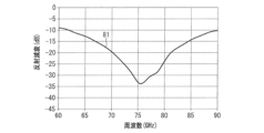
- Figure 4 shows the reflection attenuation curve of sheet 1.
- the reflection loss RL is ⁇ -19.20 dB at 76 GHz to 81 GHz, confirming that it can effectively absorb electromagnetic waves in a practical frequency range.
- the broad index indicating the width of the electromagnetic wave absorption characteristics described above is as follows: the bandwidth where the return loss is ⁇ 15 dB or less is 14.66, the minimum value RL min of the return loss in the frequency band from 60 to 90 GHz is ⁇ 26.32 dB, and the absolute value of the broad index numerical value, “minimum value of return loss/bandwidth where return loss is ⁇ 15 dB or less”, is 1.80.
- a peak value of the reflection loss exists at a frequency of 74.70 GHz, and a shoulder peak exists at a frequency of 79.50 GHz.
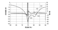
- Figure 5 shows the first, second, and third differential curves of the reflection attenuation curve of the sheet 1 shown in Figure 4.
- reference numeral 51 indicates the reflection attenuation curve of sheet 1
- reference numeral 52 indicates the first differential curve of the reflection attenuation curve of reference numeral 51
- reference numeral 53 indicates the second differential curve of the reflection attenuation curve of reference numeral 51
- reference numeral 54 indicates the third differential curve of the reflection attenuation curve of reference numeral 51.
- the first, second, and third differential values are indicated by indicators on the right side of the graph.
- the maximum absorption peak in the reflection attenuation curve of an electromagnetic wave absorbing sheet refers to the frequency at which the absolute value of the reflection attenuation is greatest among the frequencies at which the first differential curve of the reflection attenuation curve changes from negative to positive as the frequency increases, in the range of 60 GHz to 90 GHz of the incident electromagnetic wave. Since the only frequency at which the first differential curve 52 changes from negative to positive meets this definition, the reflection attenuation at a frequency of 74.70 GHz is the maximum absorption peak for sheet 1.
- the value changes from negative to positive only at the frequency of 74.70 GHz, as described above, so there is no second absorption peak in sheet 1.
- the frequency where the third differential curve 54 of the return loss curve 51 goes from positive to negative as the frequency increases is 79.50 GHz, and therefore it can be seen that the return loss curve 51 of sheet 1 has a shoulder peak at a frequency of 79.50 GHz. This can also be confirmed from the shape of the return loss curve 41 of sheet 1 shown in FIG. 4, and the return loss at this shoulder peak is approximately -22 dB. Furthermore, as shown in Table 1, the input impedance value Z of sheet 1 at a frequency of 79 GHz is 413.25 ⁇ .
- the electromagnetic wave absorbing sheet of sheet 1 satisfies the conditions for exhibiting good electromagnetic wave absorption characteristics in a wide frequency band shown in this embodiment, namely, that the impedance value Z of the entire sheet at a frequency of 79 GHz is 260 ⁇ or more and 610 ⁇ or less, that the return loss curve representing its return loss characteristics has a maximum absorption peak and a shoulder peak in the frequency band of incident electromagnetic waves from 60 GHz to 90 GHz or less, that the return loss at the maximum absorption peak is -15 dB or less and that at the shoulder peak is -10 dB or less, and that the total film thickness of the electromagnetic wave absorbing sheet is 500 ⁇ m or less.
- Figure 6 shows the reflection attenuation curve of sheet 2.
- the reflection loss RL is ⁇ -14.03 dB at 76 GHz to 81 GHz, confirming that it can effectively absorb electromagnetic waves in a practical frequency range.
- the broad index indicating the width of the electromagnetic wave absorption characteristics described above is as follows: the bandwidth where the return loss is ⁇ 15 dB or less is 7.99 GHz, the minimum value RL min of the return loss in the frequency band from 60 to 90 GHz is ⁇ 30.98 GHz, and the absolute value of the broad index numerical value, “minimum value of return loss/bandwidth where return loss is ⁇ 15 dB or less”, is 3.88.
- a peak value of reflection loss exists at a frequency of 69.60 GHz, and a second peak exists at a frequency of 81.10 GHz.
- Figure 7 shows the first differential curve, second differential curve, and third differential polarity of the reflection attenuation curve of sheet 2 shown in Figure 6.
- reference numeral 71 indicates the reflection attenuation curve of sheet 2
- reference numeral 72 indicates the first differential curve of the reflection attenuation curve of reference numeral 71
- reference numeral 73 indicates the second differential curve of the reflection attenuation curve of reference numeral 71
- reference numeral 74 indicates the third differential curve of the reflection attenuation curve of reference numeral 71.
- the first, second, and third differential values are indicated by indicators on the right side of the graph.
- the maximum absorption peak in the return loss curve of an electromagnetic wave absorbing sheet refers to the frequency at which the first differential curve of the return loss curve changes from negative to positive as the frequency increases in the range of 60 GHz to 90 GHz for incident electromagnetic waves, and the smallest numerical value of the return loss RL, i.e., the largest absolute value.
- the first differential curve 72 changes from negative to positive, at frequencies of 69.60 GHz and 81.10 GHz.
- the return loss curve indicated by reference numeral 71 has the largest return loss at a frequency of 69.60 GHz, which is a return loss of -30.98 dB, and therefore the maximum absorption peak of the return loss of sheet 2 is at a frequency of 69.60 GHz.
- the electromagnetic wave absorbing sheet of sheet 2 has a second absorption peak at a frequency of 81.10 GHz.
- the reflection attenuation curve 61 of sheet 2 shown in Figure 6 has a maximum absorption peak and a second absorption peak, and does not have a shoulder peak.
- the input impedance value Z of sheet 2 at a frequency of 79 GHz is 265.31 ⁇ .
- the electromagnetic wave absorbing sheet of sheet 2 satisfies the conditions for exhibiting good electromagnetic wave absorption characteristics in a wide frequency band shown in this embodiment, namely, the impedance value Z of the entire sheet at a frequency of 79 GHz is 260 ⁇ or more and 610 ⁇ or less, the return loss curve representing the return loss characteristics has a maximum absorption peak and a second absorption peak in a frequency band of incident electromagnetic waves from 60 GHz to 90 GHz or less, the return loss at the maximum absorption peak is -15 dB or less and the return loss at the second absorption peak is -10 dB or less, and the total thickness of the electromagnetic wave absorbing sheet is 500 ⁇ m or less.
- the second sheet whose return loss curve 61 is shown in FIG. 6, has a greater return loss at the maximum absorption peak than the first sheet shown in FIG. 4. This is thought to be due to better impedance matching at that frequency.
- Figure 8 shows the reflection attenuation curve of sheet 3.
- the reflection loss RL is ⁇ -20.48 dB from 76 GHz to 81 GHz, confirming that it can effectively absorb electromagnetic waves in a practical frequency range.
- the broad index indicating the width of the electromagnetic wave absorption characteristics described above is as follows: the bandwidth where the return loss is -15 dB or less is 17.63 GHz, the minimum value RL min of the maximum return loss in the frequency band from 60 to 90 GHz is -33.77 dB, and the absolute value of the broad index numerical value "minimum value of return loss/bandwidth where return loss is -15 dB or less" is 1.92.
- a peak value of the return loss exists at a frequency of 75.53 GHz, and a shoulder peak exists at a frequency of 78.71 GHz.
- Figure 9 shows the polarity of the first, second, and third differential curves of the reflection attenuation curve of sheet 3 shown in Figure 8.
- reference numeral 91 indicates the reflection attenuation curve of sheet 3
- reference numeral 92 indicates the first-order differential curve of the reflection attenuation curve of reference numeral 91
- reference numeral 93 indicates the second-order differential curve of the reflection attenuation curve of reference numeral 91
- reference numeral 94 indicates the third-order differential curve of the reflection attenuation curve of reference numeral 91.
- the first-order differential value, second-order differential value, and third-order differential value are indicated by indicators on the right side of the graph.
- the first derivative curve of the reflection attenuation curve changes from negative to positive as the frequency increases at a frequency of 75.53 GHz, so the reflection attenuation at a frequency of 75.53 GHz is the maximum absorption peak for Sheet 3.
- the value changes from negative to positive only at the above-mentioned frequency of 75.53 GHz, so there is no second absorption peak in sheet 3.
- the frequency at which the second-order differential curve 93 of the reflection attenuation curve 91 has a positive maximum value is 78.71 GHz, so the reflection attenuation curve 91 of sheet 3 has a shoulder peak at a frequency of 79.50 GHz.
- the input impedance value Z of sheet 3 at a frequency of 79 GHz is 406.27 ⁇ .
- the electromagnetic wave absorbing sheet of sheet 3 satisfies the conditions for exhibiting good electromagnetic wave absorption characteristics in a wide frequency band shown in this embodiment, namely, that the impedance value Z of the entire sheet at a frequency of 79 GHz is 260 ⁇ or more and 610 ⁇ or less, the return loss curve representing its return loss characteristics has a maximum absorption peak and a shoulder peak in the frequency band of incident electromagnetic waves from 60 GHz to 90 GHz or less, the return loss at the maximum absorption peak is -15 dB or less and the return loss at the shoulder peak is -10 dB or less, and the total thickness of the electromagnetic wave absorbing sheet is 500 ⁇ m or less.
- Figure 10 shows the reflection attenuation curve of sheet 4.
- the minimum reflection loss between 76 GHz and 81 GHz is -6.58 dB, which shows that the sheet is unable to effectively absorb electromagnetic waves in a practical frequency range.
- the return loss curve 101 of sheet 4 shown in Figure 10 shows a tendency for the return loss to gradually decrease as the frequency increases, i.e., for the return loss RL to increase.
- the first derivative curve of the return loss curve shown in Figure 5 does not have any portion where the value changes from negative to positive, and it was confirmed that there is no absorption peak in the return loss curve shown in Figure 5.
- Sheet 4 which shows this kind of return loss curve, has an impedance value Z of 219.21 for the entire sheet at a frequency of 79 GHz, which does not meet the requirement of 260 ⁇ or more and 610 ⁇ or less, and the return loss curve, which shows its return loss characteristics, does not show a maximum absorption peak, and only has a portion that meets the condition of a shoulder peak at a frequency of 79.60 GHz.
- the total thickness of the electromagnetic wave absorbing sheet of Sheet 4 is 338 ⁇ m, so it meets the requirement that the layer thickness be 500 ⁇ m or less, but the absolute value of the index showing that it has broad electromagnetic wave absorption characteristics, "minimum return loss value/bandwidth where return loss is -15 dB or less,” is 9.12, which is greater than 4.00.
- the electromagnetic wave absorbing sheet of Sheet 4 corresponds to a comparative example that does not meet the preferable requirements of the electromagnetic wave absorbing sheet disclosed in the present application, and that its electromagnetic wave absorbing characteristics are not capable of effectively absorbing electromagnetic waves in a wide frequency band.
- Figure 11 shows the reflection attenuation curve of sheet 5.
- the reflection loss RL is ⁇ -26.67 dB at 76 GHz to 81 GHz, confirming that it can effectively absorb electromagnetic waves in a practical frequency range.
- the broad index indicating the width of the electromagnetic wave absorption characteristics described above is as follows: the bandwidth where the return loss is -15 dB or less is 15.00 GHz, the minimum value RL min of the maximum return loss in the frequency band from 60 to 90 GHz is -40.79 dB, and the absolute value of the broad index numerical value "minimum value of return loss/bandwidth where return loss is -15 dB or less" is 2.72.
- a peak value of the reflection loss exists at a frequency of 74.85 GHz, and a second peak exists at a frequency of 80.55 GHz.
- FIG. 12 shows the first, second, and third derivative curves of the reflection attenuation curve of the sheet 5 shown in FIG. 11.
- reference numeral 121 indicates the reflection attenuation curve of sheet 5
- reference numeral 122 indicates the first differential curve of the reflection attenuation curve of reference numeral 121
- reference numeral 123 indicates the second differential curve of the reflection attenuation curve of reference numeral 121
- reference numeral 124 indicates the third differential curve of the reflection attenuation curve of reference numeral 121. Note that, as in FIG. 5, FIG. 7, and FIG. 9, the first differential value, the second differential value, and the third differential value are indicated by indicators on the right side of the graph.
- the return loss curve indicated by reference numeral 121 has a large return loss of -40.79 dB at a frequency of 74.85 GHz, and therefore the maximum absorption peak of the return loss of sheet 5 is at a frequency of 74.85 GHz.
- the electromagnetic wave absorbing sheet of sheet 5 has a second absorption peak at a frequency of 80.55 GHz.
- the return loss curve 111 of the sheet 5 shown in Fig. 11 It can also be confirmed from the return loss curve 111 of the sheet 5 shown in Fig. 11 that the return loss curve of the second sheet has a maximum absorption peak and a second absorption peak, and has no shoulder peak. As shown in Table 1, the input impedance value Z of the sheet 5 at a frequency of 79 GHz is 352.48 ⁇ .
- the electromagnetic wave absorbing sheet of the sheet 5 satisfies the conditions for exhibiting good electromagnetic wave absorbing characteristics in a wide frequency band shown in this embodiment, that is, the impedance value Z of the entire sheet at a frequency of 79 GHz is 260 ⁇ or more and 610 ⁇ or less, the return loss curve representing the return loss characteristics has a maximum absorption peak and a second absorption peak in a frequency band of incident electromagnetic waves from 60 GHz to 90 GHz, the return loss at the maximum absorption peak is -15 dB or less, the return loss at the second absorption peak is -10 dB or less, and the total thickness of the electromagnetic wave absorbing sheet is 500 ⁇ m or less.
- the absolute value of "minimum return loss/bandwidth where return loss is -15 dB or less” is 2.72, which satisfies the condition of 4.00 or less, indicating good absorption of electromagnetic waves over a wide frequency band.
- the half-width of the peak in the curve showing the change in the value of the imaginary part of the relative magnetic permeability ( ⁇ r'') with respect to the frequency of 60 GHz to 90 GHz is a small value of 5.4. This is considered to be caused by the particle size distribution of epsilon iron oxide being smaller than that of hexagonal ferrite.
- the reflection attenuation curve showing the reflection attenuation characteristics of the obtained electromagnetic wave absorbing sheet does not have either a shoulder peak or a second absorption peak in addition to the maximum absorption peak. Furthermore, even if either a shoulder peak or a second absorption peak is present, it is considered that the reflection attenuation in the frequency band of 76 GHz to 81 GHz will not be -15 dB or less.
- an electromagnetic wave absorbing sheet with a wide half-value width of the imaginary part of the relative permeability of a magnetic layer will have a relatively wide absorption band when tuned to absorb at the desired center frequency, making it possible to realize an electromagnetic wave absorbing sheet that is suitable for practical use.
- the electromagnetic wave absorbing sheet shown in this embodiment has a characteristic configuration in which the magnetic iron oxide contained in the magnetic layer is hexagonal ferrite, the overall input impedance Z is 260 ⁇ or more and 610 ⁇ or less, the return loss curve has at least one of a maximum absorption peak, a shoulder peak, and a second absorption peak smaller than the maximum absorption peak in a frequency band in which the frequency of the incident electromagnetic wave is 60 GHz or more and 90 GHz or less, the return loss at the maximum absorption peak is -15 dB or less, and the return loss at the shoulder peak or the second peak is -10 dB or less, and the total film thickness of the electromagnetic wave absorbing sheet is 500 ⁇ m or less, and therefore can satisfy the condition that the absolute value of "minimum return loss value/bandwidth where return loss value is -15 dB or less", which is an index of an electromagnetic wave absorbing sheet having broad electromagnetic wave absorption characteristics, is 4.00 or less.
- the electromagnetic wave absorbing sheet disclosed in this application contains hexagonal ferrite as magnetic iron oxide in the magnetic layer, and the reflection attenuation curve showing the electromagnetic wave absorption characteristics in the frequency band of 60 GHz or more and 90 GHz or less includes a maximum peak value and either a shoulder peak or a second peak, making it an electromagnetic wave absorbing sheet that can exhibit good electromagnetic wave absorption characteristics in a wide frequency band, and is particularly useful in practical fields such as in-vehicle radar.
- the electromagnetic wave absorbing sheet disclosed in this application can contribute to achieving Goal 9 (build resilient infrastructure, promote inclusive and sustainable industrialization, innovate and innovate), one of the 17 Sustainable Development Goals (SDGs) established by the United Nations.
- Goal 9 build resilient infrastructure, promote inclusive and sustainable industrialization, innovate and innovate
- SDGs 17 Sustainable Development Goals
Landscapes
- Engineering & Computer Science (AREA)
- Chemical & Material Sciences (AREA)
- Dispersion Chemistry (AREA)
- Power Engineering (AREA)
- Microelectronics & Electronic Packaging (AREA)
- Shielding Devices Or Components To Electric Or Magnetic Fields (AREA)
Priority Applications (1)
| Application Number | Priority Date | Filing Date | Title |
|---|---|---|---|
| JP2025535859A JPWO2025023278A1 (https=) | 2023-07-25 | 2024-07-24 |
Applications Claiming Priority (2)
| Application Number | Priority Date | Filing Date | Title |
|---|---|---|---|
| JP2023120986 | 2023-07-25 | ||
| JP2023-120986 | 2023-07-25 |
Publications (1)
| Publication Number | Publication Date |
|---|---|
| WO2025023278A1 true WO2025023278A1 (ja) | 2025-01-30 |
Family
ID=94374620
Family Applications (1)
| Application Number | Title | Priority Date | Filing Date |
|---|---|---|---|
| PCT/JP2024/026477 Pending WO2025023278A1 (ja) | 2023-07-25 | 2024-07-24 | 電磁波吸収シート |
Country Status (2)
| Country | Link |
|---|---|
| JP (1) | JPWO2025023278A1 (https=) |
| WO (1) | WO2025023278A1 (https=) |
Citations (3)
| Publication number | Priority date | Publication date | Assignee | Title |
|---|---|---|---|---|
| JP2007250823A (ja) * | 2006-03-16 | 2007-09-27 | Dowa Holdings Co Ltd | 電波吸収体用磁性粉体および製造法並びに電波吸収体 |
| JP2016111341A (ja) * | 2014-12-03 | 2016-06-20 | 国立大学法人 東京大学 | 電磁波吸収体及び膜形成用ペースト |
| WO2018168859A1 (ja) * | 2017-03-13 | 2018-09-20 | マクセルホールディングス株式会社 | 電磁波吸収シート |
-
2024
- 2024-07-24 WO PCT/JP2024/026477 patent/WO2025023278A1/ja active Pending
- 2024-07-24 JP JP2025535859A patent/JPWO2025023278A1/ja active Pending
Patent Citations (3)
| Publication number | Priority date | Publication date | Assignee | Title |
|---|---|---|---|---|
| JP2007250823A (ja) * | 2006-03-16 | 2007-09-27 | Dowa Holdings Co Ltd | 電波吸収体用磁性粉体および製造法並びに電波吸収体 |
| JP2016111341A (ja) * | 2014-12-03 | 2016-06-20 | 国立大学法人 東京大学 | 電磁波吸収体及び膜形成用ペースト |
| WO2018168859A1 (ja) * | 2017-03-13 | 2018-09-20 | マクセルホールディングス株式会社 | 電磁波吸収シート |
Non-Patent Citations (1)
| Title |
|---|
| 乾 哲司, 六方晶Mg2Yフェライトを用いた広帯域電波吸収体, 電子情報通信学会1999年総合大会 通信1, 08 March 1999, non-official translation (INUI, Tetsuji, Wideband Radio Wave Absorber Using Hexagonal Mg2Y Ferrite, The Institute of Electronics, Information and Communication Engineers General Conference 1999, Communication 1) * |
Also Published As
| Publication number | Publication date |
|---|---|
| JPWO2025023278A1 (https=) | 2025-01-30 |
Similar Documents
| Publication | Publication Date | Title |
|---|---|---|
| Zahid et al. | M-type barium hexaferrite-based nanocomposites for EMI shielding application: a review | |
| JP7267912B2 (ja) | 電磁波吸収シート | |
| JP2022115987A (ja) | 電磁波吸収シート | |
| WO2017221992A1 (ja) | 電波吸収シート | |
| Gupta et al. | Microwave absorption in X and Ku band frequency of cotton fabric coated with Ni–Zn ferrite and carbon formulation in polyurethane matrix | |
| US11985805B2 (en) | Thermally conductive electromagnetically absorptive material | |
| RU2370866C1 (ru) | Радиопоглощающее покрытие | |
| Bora et al. | Polyvinylbutyral–polyaniline nanocomposite for high microwave absorption efficiency | |
| KR20030007398A (ko) | 전파 흡수체 | |
| US20250183545A1 (en) | Radio wave reflector | |
| KR102123786B1 (ko) | 전자파 흡수 복합 시트 | |
| WO2025023278A1 (ja) | 電磁波吸収シート | |
| JP2000244167A (ja) | 電磁波障害防止材 | |
| EP4290995A1 (en) | Radio wave absorber and radio wave absorbing device | |
| JP7739801B2 (ja) | 積層シート、電磁波抑制体、電機製品、通信機器、及び交通機関 | |
| JPWO2025023278A5 (https=) | ||
| US12349328B2 (en) | Electric-wave absorber and manufacturing method for electric-wave absorber | |
| JP2002374091A (ja) | 電波吸収材料およびそれを用いた電波吸収体 | |
| WO2025028488A1 (ja) | 電磁波吸収体 | |
| JPWO2022158562A5 (https=) | ||
| JPWO2025028488A5 (https=) | ||
| KR102720707B1 (ko) | 초광대역 전자파 흡수시트, 이의 제조방법 및 이를 포함하는 물품 | |
| JP7854778B2 (ja) | レーダーユニット用積層シート | |
| TWI501866B (zh) | Conductive polymer broadband microwave absorbing body | |
| KR101455116B1 (ko) | 차량용 레이더에 사용되는 전자파 흡수체 및 이의 제조방법. |
Legal Events
| Date | Code | Title | Description |
|---|---|---|---|
| 121 | Ep: the epo has been informed by wipo that ep was designated in this application |
Ref document number: 24845653 Country of ref document: EP Kind code of ref document: A1 |
|
| ENP | Entry into the national phase |
Ref document number: 2025535859 Country of ref document: JP Kind code of ref document: A |
|
| WWE | Wipo information: entry into national phase |
Ref document number: 2025535859 Country of ref document: JP |
|
| NENP | Non-entry into the national phase |
Ref country code: DE |