WO2025023007A1 - 電力変換装置 - Google Patents
電力変換装置 Download PDFInfo
- Publication number
- WO2025023007A1 WO2025023007A1 PCT/JP2024/024758 JP2024024758W WO2025023007A1 WO 2025023007 A1 WO2025023007 A1 WO 2025023007A1 JP 2024024758 W JP2024024758 W JP 2024024758W WO 2025023007 A1 WO2025023007 A1 WO 2025023007A1
- Authority
- WO
- WIPO (PCT)
- Prior art keywords
- period
- control
- switching
- power conversion
- switching element
- Prior art date
- Legal status (The legal status is an assumption and is not a legal conclusion. Google has not performed a legal analysis and makes no representation as to the accuracy of the status listed.)
- Pending
Links
Images


Classifications
-
- H—ELECTRICITY
- H02—GENERATION; CONVERSION OR DISTRIBUTION OF ELECTRIC POWER
- H02M—APPARATUS FOR CONVERSION BETWEEN AC AND AC, BETWEEN AC AND DC, OR BETWEEN DC AND DC, AND FOR USE WITH MAINS OR SIMILAR POWER SUPPLY SYSTEMS; CONVERSION OF DC OR AC INPUT POWER INTO SURGE OUTPUT POWER; CONTROL OR REGULATION THEREOF
- H02M7/00—Conversion of AC power input into DC power output; Conversion of DC power input into AC power output
- H02M7/42—Conversion of DC power input into AC power output without possibility of reversal
- H02M7/44—Conversion of DC power input into AC power output without possibility of reversal by static converters
- H02M7/48—Conversion of DC power input into AC power output without possibility of reversal by static converters using discharge tubes with control electrode or semiconductor devices with control electrode
Definitions
- This disclosure relates to a power conversion device, and more specifically, to a power conversion device capable of converting DC power to AC power.
- the power conversion device disclosed in Patent Document 1 includes a first DC terminal and a second DC terminal, a power conversion circuit, a plurality of AC terminals, a plurality of switches, a plurality of resonant capacitors, a resonant inductor, a capacitor, and a control device.
- the power conversion circuit has a plurality of first switching elements and a plurality of second switching elements.
- a plurality of switching circuits in which a plurality of first switching elements and a plurality of second switching elements are connected in series in a one-to-one relationship, are connected in parallel to each other.
- the plurality of switches correspond one-to-one to the plurality of switching circuits, and a first end is connected to a connection point of the first switching element and the second switching element in the corresponding switching circuit, and a second end is commonly connected to a common connection point.
- a first end of the resonant inductor is connected to the common connection point.
- the power conversion device disclosed in Patent Document 1 can perform soft switching more reliably.
- the objective of this disclosure is to provide a power conversion device that can reduce current distortion.
- a power conversion device includes a first DC terminal and a second DC terminal, a power conversion circuit, a plurality of AC terminals, a plurality of switches, a plurality of resonant capacitors, a resonant inductor, a regenerative capacitor, and a control device.
- the power conversion circuit has a plurality of first switching elements and a plurality of second switching elements.
- a plurality of switching circuits in which the plurality of first switching elements and the plurality of second switching elements are connected in series in a one-to-one relationship are connected in parallel to each other.
- the plurality of first switching elements are connected to the first DC terminal, and the plurality of second switching elements are connected to the second DC terminal.
- the plurality of AC terminals correspond one-to-one to the plurality of switching circuits.
- Each of the plurality of AC terminals is connected to a connection point of the first switching element and the second switching element in the corresponding switching circuit.
- the plurality of switches correspond one-to-one to the plurality of switching circuits.
- Each of the plurality of switches has a first end connected to the connection point of the first switching element and the second switching element in the corresponding switching circuit, and a second end commonly connected to a common connection point.
- the resonance capacitors correspond one-to-one to the plurality of switches.
- Each of the plurality of resonance capacitors is connected between the first end and the second DC terminal of the corresponding switch.
- the resonance inductor has a first end and a second end. The first end of the resonance inductor is connected to the common connection point.
- the regeneration capacitor has a third end and a fourth end. The third end of the regeneration capacitor is connected to the first DC terminal or the second DC terminal.
- the control device provides a control signal whose potential changes between a high level and a low level to each of the plurality of first switching elements, the plurality of second switching elements, and the plurality of switches.
- the control device sets a dead time period between a high level period of a control signal to the first switching element and a high level period of a control signal to the second switching element for each of the multiple switching circuits, and sets the high level period of the control signal to each of the multiple switches based on the dead time period for the corresponding switching circuit among the multiple switching circuits.
- the control device determines that a resonant current flows through two or more switches of the multiple switches simultaneously in the resonant inductor
- the control device is configured to perform one of a first control operation and a second control operation based on an overlap period during which the resonant current flows through each of the two or more switches simultaneously.
- the first control operation is an operation of shifting a high level period of a control signal to at least one of the two or more switches so that the resonant current does not flow through the resonant inductor simultaneously.
- the second control operation is an operation of shifting a high level period of a control signal to at least one of the two or more switches so that the high level period of the control signal to each of the two or more switches overlaps a predetermined period or more in a dead time period corresponding to each of two or more switching circuits connected to the two or more switches among the multiple switching circuits.
- the power conversion device disclosed herein has the effect of making it possible to reduce current distortion.
- FIG. 1 is a circuit diagram of a system including a power conversion device according to a first embodiment.
- FIG. 2 is an explanatory diagram of an operation when the control device in the power conversion device of the first embodiment performs a basic operation in the case where the load current is greater than 0 and the resonance capacitor is being charged.
- FIG. 3 is another operation explanatory diagram when the control device in the power conversion device of the first embodiment performs a basic operation in the case where the load current is greater than 0 and the resonance capacitor is being charged.
- FIG. 4 is another operation explanatory diagram when the control device in the power conversion device of the first embodiment performs a basic operation in the case where the load current is greater than 0 and the resonance capacitor is being charged.
- FIG. 1 is a circuit diagram of a system including a power conversion device according to a first embodiment.
- FIG. 2 is an explanatory diagram of an operation when the control device in the power conversion device of the first embodiment performs a basic operation in the case where the load current is greater than 0 and the
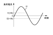
- FIG. 5 is a diagram showing a time change in duty corresponding to a voltage command for each of three phases in an AC load connected to a plurality of AC terminals of the power conversion device of the first embodiment, and a time change in load current.
- FIG. 6 is an explanatory diagram of the first current threshold value and the second current threshold value used by the control device in the power conversion device of the first embodiment.
- FIG. 7 is an explanatory diagram of an operation when the control device in the power conversion device of the first embodiment performs a basic operation in the case where the load current is greater than 0 and the resonant capacitor is discharging.
- FIG. 8 is an explanatory diagram of an operation when the control device in the power conversion device of the first embodiment performs a basic operation when the load current is less than 0 and the resonance capacitor is discharging.
- FIG. 9 is an explanatory diagram of an operation when the control device in the power conversion device of the first embodiment performs a basic operation in the case where the load current is less than 0 and the resonance capacitor is being charged.
- FIG. 10 is a timing chart for explaining an example of boundary conditions between a case where currents flowing through the resonant inductors do not overlap (do not flow simultaneously) and a case where currents flow through the resonant inductors overlap (flow simultaneously) in the power conversion device of embodiment 1.
- FIG. 11 is a timing chart for explaining an example of boundary conditions when the U-phase resonant current and the V-phase resonant current do not overlap (do not flow simultaneously) and when they overlap (flow simultaneously) in the power conversion device of embodiment 1.
- FIG. 12 is a timing chart for explaining an operation when the control device performs the first control operation in the power conversion device of the first embodiment.
- FIG. 13 is a waveform diagram of the load current in the power conversion device of the first embodiment.
- FIG. 14 is a timing chart for explaining the operation when the control device performs the second control operation in the power conversion device of the first embodiment.
- FIG. 15 is a timing chart for explaining the operation when the control device performs the first control operation in the power conversion device according to the second embodiment.
- FIG. 12 is a timing chart for explaining an operation when the control device performs the first control operation in the power conversion device of the first embodiment.
- FIG. 13 is a waveform diagram of the load current in the power conversion device of the first embodiment.
- FIG. 14 is
- FIG. 16 is a timing chart for explaining the operation when the control device performs the second control operation in the power conversion device of the second embodiment.
- FIG. 17 is a timing chart for explaining the operation when the control device performs the first control operation in the power conversion device according to the third embodiment.
- FIG. 18 is a timing chart for explaining the operation when the control device performs the second control operation in the power conversion device of the third embodiment.
- FIG. 19 is a circuit diagram of a system including a power conversion device according to the fourth embodiment.
- FIG. 20 is a circuit diagram of a system including a power conversion device according to the fifth embodiment.
- FIG. 21 is a circuit diagram of a system including a power conversion device according to the sixth embodiment.
- FIG. 22 is a circuit diagram of a system including a power conversion device according to the seventh embodiment.
- FIG. 23 is a circuit diagram of a system including a power conversion device according to the eighth embodiment.
- FIG. 24 is a circuit diagram of a system including a power conversion device according to the ninth embodiment.
- FIG. 25 is a circuit diagram of a system including a power conversion device according to the tenth embodiment.
- FIG. 26 is a circuit diagram of a system including a power conversion device according to the eleventh embodiment.
- FIG. 27 is a timing chart for explaining the operation when the control device in the power conversion device according to example 1 performs the second control operation.
- FIG. 28 is a timing chart for explaining the operation when the control device in the power conversion device of Example 1 performs the first control operation.
- FIG. 29 is a timing chart for explaining the operation when the control device in the power conversion device according to the second example performs the second control operation.
- FIG. 30 is a timing chart for explaining the operation when the control device in the power conversion device of Example 2 performs the first control operation.
- FIG. 31 is a timing chart for explaining the operation when the control device in the power conversion device according to Example 3 performs the second control operation.
- FIG. 32 is a timing chart for explaining the operation when the control device in the power conversion device of Example 3 performs the first control operation.
- FIG. 1 is a circuit diagram of a system including a power conversion device 100 according to the first embodiment.
- the power conversion device 100 includes a first DC terminal 31, a second DC terminal 32, and a plurality of (for example, three) AC terminals 41.
- a DC power source E1 is connected between the first DC terminal 31 and the second DC terminal 32, and an AC load RA1 is connected to the plurality of AC terminals 41.
- the AC load RA1 is, for example, a three-phase servo motor.
- the power conversion device 100 converts the DC output from the DC power source E1 into AC power and outputs it to the AC load RA1.
- the DC power source E1 includes, for example, a solar cell or a fuel cell.
- the DC power source E1 may include a DC-DC converter.
- the AC power is, for example, three-phase AC power having a U phase, a V phase, and a W phase.
- the power conversion device 100 includes a power conversion circuit 11, a plurality of (e.g., three) switches 8, a plurality of (e.g., three) resonant capacitors 9, a resonant inductor L1, a regenerative capacitor 15, and a control device 50.
- the power conversion device 100 further includes a protection circuit 17 and a capacitor C10.
- Each of the plurality of switches 8 is, for example, a bidirectional switch.
- the power conversion circuit 11 has a plurality of (e.g., three) first switching elements 1 and a plurality of (e.g., three) second switching elements 2.
- a plurality of (e.g., three) switching circuits 10 in which a plurality of first switching elements 1 and a plurality of second switching elements 2 are connected in series in a one-to-one relationship are connected in parallel to each other.
- a plurality of first switching elements 1 are connected to a first DC terminal 31, and a plurality of second switching elements 2 are connected to a second DC terminal 32.
- a plurality of AC terminals 41 correspond one-to-one to the plurality of switching circuits 10.
- Each of the plurality of AC terminals 41 is connected to a connection point 3 of the first switching element 1 and the second switching element 2 in the corresponding switching circuit 10.
- a plurality of switches 8 correspond one-to-one to the plurality of switching circuits 10.
- Each of the plurality of switches 8 has a first end 81 connected to a connection point 3 of the first switching element 1 and the second switching element 2 in the corresponding switching circuit 10, and a second end 82 commonly connected to a common connection point 25.
- the multiple resonant capacitors 9 correspond one-to-one to the multiple switches 8.
- Each of the multiple resonant capacitors 9 is connected between the first end 81 of the corresponding switch 8 and the second DC terminal 32.
- the resonant inductor L1 has a first end and a second end.
- the first end of the resonant inductor L1 is connected to the common connection point 25.
- the regenerative capacitor 15 has a third end 153 and a fourth end 154.
- the third end 153 is connected to the second DC terminal 32
- the fourth end 154 is connected to the common connection point 25 via the resonant inductor L1.
- the control device 50 controls the multiple first switching elements 1, the multiple second switching elements 2, and the multiple switches 8.
- the switching circuits 10 corresponding to the U-phase, V-phase, and W-phase of the multiple switching circuits 10 may be referred to as a switching circuit 10U, a switching circuit 10V, and a switching circuit 10W, respectively.
- the first switching element 1 and the second switching element 2 of the switching circuit 10U may be referred to as a first switching element 1U and a second switching element 2U.
- the first switching element 1 and the second switching element 2 of the switching circuit 10V may be referred to as a first switching element 1V and a second switching element 2V.
- the first switching element 1 and the second switching element 2 of the switching circuit 10W may be referred to as a first switching element 1W and a second switching element 2W.
- the connection point 3 between the first switching element 1U and the second switching element 2U may be referred to as the connection point 3U
- the connection point 3 between the first switching element 1V and the second switching element 2V may be referred to as the connection point 3V
- the connection point 3 between the first switching element 1W and the second switching element 2W may be referred to as the connection point 3W.
- the AC terminal 41 connected to the connection point 3U may be referred to as the AC terminal 41U
- the AC terminal 41 connected to the connection point 3V may be referred to as the AC terminal 41V
- the AC terminal 41 connected to the connection point 3W may be referred to as the AC terminal 41W.
- the resonant capacitor 9 connected in parallel to the second switching element 2U may be referred to as the resonant capacitor 9U
- the resonant capacitor 9 connected in parallel to the second switching element 2V may be referred to as the resonant capacitor 9V
- the resonant capacitor 9 connected in parallel to the second switching element 2W may be referred to as the resonant capacitor 9W.
- switch 8U the switch 8 connected to connection point 3U
- switch 8V the switch 8 connected to connection point 3V
- switch 8W the switch 8 connected to connection point 3W
- the high-potential output terminal (positive electrode) of the DC power source E1 is connected to the first DC terminal 31, and the low-potential output terminal (negative electrode) of the DC power source E1 is connected to the second DC terminal 32.
- the U-phase terminal, V-phase terminal, and W-phase terminal of the AC load RA1 are connected to the three AC terminals 41U, 41V, and 41W, respectively.
- each of the multiple (e.g., three) first switching elements 1 and the multiple (e.g., three) second switching elements 2 has a control terminal, a first main terminal, and a second main terminal.
- the control terminals of the multiple first switching elements 1 and the multiple second switching elements 2 are connected to the control device 50.
- the first main terminal of the first switching element 1 is connected to the first DC terminal 31
- the second main terminal of the first switching element 1 is connected to the first main terminal of the second switching element 2
- the second main terminal of the second switching element 2 is connected to the second DC terminal 32.
- the first switching element 1 is a high-side switching element (P-side switching element), and the second switching element 2 is a low-side switching element (N-side switching element).
- Each of the multiple first switching elements 1 and the multiple second switching elements 2 is, for example, an IGBT (Insulated Gate Bipolar Transistor). Therefore, the control terminal, the first main terminal, and the second main terminal of each of the multiple first switching elements 1 and the multiple second switching elements 2 are the gate terminal, the collector terminal, and the emitter terminal, respectively.
- the power conversion circuit 11 further includes a plurality (three) of first diodes 4 connected in anti-parallel to a plurality (three) of first switching elements 1 in a one-to-one relationship, and a plurality (three) of second diodes 5 connected in anti-parallel to a plurality (three) of second switching elements 2 in a one-to-one relationship.
- the anode of the first diode 4 is connected to the second main terminal (emitter terminal) of the first switching element 1 corresponding to the first diode 4
- the cathode of the first diode 4 is connected to the first main terminal (collector terminal) of the first switching element 1 corresponding to the first diode 4.
- the anode of the second diode 5 is connected to the second main terminal (emitter terminal) of the second switching element 2 corresponding to the second diode 5, and the cathode of the second diode 5 is connected to the first main terminal (collector terminal) of the second switching element 2 corresponding to the second diode 5.
- connection point 3U between the first switching element 1U and the second switching element 2U is connected to, for example, the U-phase terminal of the AC load RA1 via the AC terminal 41U.
- connection point 3V between the first switching element 1V and the second switching element 2V is connected to, for example, the V-phase of the AC load RA1 via the AC terminal 41V.
- connection point 3W between the first switching element 1W and the second switching element 2W is connected to, for example, the W-phase of the AC load RA1 via the AC terminal 41W.
- the multiple resonant capacitors 9 correspond one-to-one to the multiple switches 8. Each of the multiple resonant capacitors 9 is connected between the first end of the corresponding switch 8 and the second DC terminal 32.
- the power conversion device 100 has multiple resonant circuits.
- the multiple resonant circuits include a resonant circuit having a resonant capacitor 9U and a resonant inductor L1, a resonant circuit having a resonant capacitor 9V and a resonant inductor L1, and a resonant circuit having a resonant capacitor 9W and a resonant inductor L1.
- the multiple resonant circuits share the resonant inductor L1 in common.
- Each of the multiple switches 8 has, for example, two first IGBTs 6 and second IGBTs 7 connected in inverse parallel.
- the collector terminal of the first IGBT 6 is connected to the emitter terminal of the second IGBT 7, and the emitter terminal of the first IGBT 6 is connected to the collector terminal of the second IGBT 7.
- the emitter terminal of the first IGBT 6 is connected to the connection point 3 of the switching circuit 10 corresponding to the switch 8 having the first IGBT 6.
- the collector terminal of the second IGBT 7 is connected to the connection point 3 of the switching circuit 10 corresponding to the switch 8 having the second IGBT 7.
- the switch 8U is connected to the connection point 3U of the first switching element 1U and the second switching element 2U.
- the switch 8V is connected to the connection point 3V of the first switching element 1V and the second switching element 2V.
- the switch 8W is connected to a connection point 3W between the first switching element 1W and the second switching element 2W.
- the first IGBT 6 and the second IGBT 7 of the switch 8U are referred to as the first IGBT 6U and the second IGBT 7U, respectively
- the first IGBT 6 and the second IGBT 7 of the switch 8V are referred to as the first IGBT 6V and the second IGBT 7V, respectively
- the first IGBT 6 and the second IGBT 7 of the switch 8W are referred to as the first IGBT 6W and the second IGBT 7W, respectively.
- the multiple switches 8 are controlled by the control device 50.
- the first IGBT 6U, the second IGBT 7U, the first IGBT 6V, the second IGBT 7V, the first IGBT 6W, and the second IGBT 7W are controlled by the control device 50.
- the resonant inductor L1 has a first end and a second end. In the resonant inductor L1, the first end of the resonant inductor L1 is connected to the common connection point 25. The second end of the resonant inductor L1 is connected to the fourth end 154 of the regenerative capacitor 15.
- the regenerative capacitor 15 is connected between the second end of the resonant inductor L1 and the second DC terminal 32.
- the regenerative capacitor 15 is, for example, a film capacitor.
- the protection circuit 17 includes a third diode 13 and a fourth diode 14.
- the third diode 13 is connected between the common connection point 25 and the first DC terminal 31.
- the anode of the third diode 13 is connected to the common connection point 25.
- the cathode of the third diode 13 is connected to the first DC terminal 31.
- the fourth diode 14 is connected between the common connection point 25 and the second DC terminal 32.
- the anode of the fourth diode 14 is connected to the second DC terminal 32.
- the cathode of the fourth diode 14 is connected to the common connection point 25. Therefore, the fourth diode 14 is connected in series with the third diode 13.
- Capacitor C10 is connected between the first DC terminal 31 and the second DC terminal 32, and is connected in parallel to the power conversion circuit 11.
- Capacitor C10 is, for example, an electrolytic capacitor.
- the control device 50 controls a plurality of first switching elements 1, a plurality of second switching elements 2, and a plurality of switches 8.
- the execution subject of the control device 50 includes a computer system.
- the computer system has one or more computers.
- the computer system is mainly composed of a processor and a memory as hardware.
- the processor executes a program recorded in the memory of the computer system, thereby realizing the function of the control device 50 as the execution subject in the present disclosure.
- the program may be pre-recorded in the memory of the computer system, or may be provided through an electric communication line, or may be recorded and provided on a non-transitory recording medium such as a memory card, an optical disk, or a hard disk drive (magnetic disk) that can be read by the computer system.
- the processor of the computer system is composed of one or more electronic circuits including a semiconductor integrated circuit (Integrated Circuit, IC) or a large scale integrated circuit (Large Scale Integration, LSI).
- the multiple electronic circuits may be integrated in one chip or distributed across multiple chips.
- the multiple chips may be integrated in one device or distributed across multiple devices.
- the control device 50 outputs control signals SU1, SV1, SW1 that control the on/off of each of the multiple first switching elements 1U, 1V, 1W.
- Each of the control signals SU1, SV1, SW1 is, for example, a PWM (Pulse Width Modulation) signal whose potential level changes between a first potential level (hereinafter also referred to as a low level) and a second potential level (hereinafter also referred to as a high level) that is higher than the first potential level.
- the first switching elements 1U, 1V, 1W are in an on state when the control signals SU1, SV1, SW1 are at a high level, and in an off state when the control signals are at a low level.
- the control device 50 also outputs control signals SU2, SV2, SW2 that control the on/off of each of the multiple second switching elements 2U, 2V, 2W.
- Each of the control signals SU2, SV2, and SW2 is, for example, a PWM signal whose potential level changes between a first potential level (hereinafter also referred to as a low level) and a second potential level (hereinafter also referred to as a high level) that is higher than the first potential level.
- the second switching elements 2U, 2V, and 2W are turned on when the control signals SU2, SV2, and SW2 are at a high level, and turned off when they are at a low level.
- the control device 50 uses a sawtooth carrier signal (see FIG. 2 and FIG. 11) to generate control signals SU1, SV1, SW1 corresponding to the first switching elements 1U, 1V, 1W, respectively, and control signals SU2, SV2, SW2 corresponding to the second switching elements 2U, 2V, 2W, respectively. More specifically, the control device 50 generates control signals SU1, SU2 to be given to the first switching element 1U and the second switching element 2U, respectively, based on at least the carrier signal and a voltage command of the U phase. The control device 50 also generates control signals SV1, SV2 to be given to the first switching element 1V and the second switching element 2V, respectively, based on at least the carrier signal and a voltage command of the V phase.
- a sawtooth carrier signal see FIG. 2 and FIG. 11
- the control device 50 also generates control signals SW1, SW2 to be given to the first switching element 1W and the second switching element 2W, respectively, based on at least the carrier signal and a voltage command of the W phase.
- the U-phase voltage command, V-phase voltage command, and W-phase voltage command are, for example, sinusoidal signals with a phase difference of 120° from each other, and each value (voltage command value) changes over time.
- the waveform of the carrier signal is not limited to a sawtooth waveform, and may be, for example, a triangular wave, or a sawtooth wave with the left and right reversed as shown in FIG. 11.
- the length of one cycle of the U-phase voltage command, V-phase voltage command, and W-phase voltage command is the same.
- the length of one cycle of the U-phase voltage command, V-phase voltage command, and W-phase voltage command is longer than the length of one cycle of the carrier signal.
- the duty of the control signal SU1 is shown as the U-phase duty.
- the control device 50 compares the U-phase voltage command with the carrier signal to generate the control signal SU1 to be provided to the first switching element 1U.
- the control device 50 also inverts the control signal SU1 to be provided to the first switching element 1U to generate the control signal SU2 to be provided to the second switching element 2U.
- the control device 50 also sets a dead time period Td (see FIG. 2) between the high-level period of the control signal SU1 and the high-level period of the control signal SU2 so that the on periods of the first switching element 1U and the second switching element 2U do not overlap.
- the duty of the control signal SV1 is shown as the V-phase duty.
- the control device 50 compares the V-phase voltage command with the carrier signal to generate the control signal SV1 to be provided to the first switching element 1V.
- the control device 50 also inverts the control signal SV1 to be provided to the first switching element 1V to generate the control signal SV2 to be provided to the second switching element 2V.
- the control device 50 also sets a dead time period Td (see FIG. 3) between the high-level period of the control signal SV1 and the high-level period of the control signal SV2 so that the on periods of the first switching element 1V and the second switching element 2V do not overlap.
- the duty of the control signal SW1 is shown as the W phase duty.
- the control device 50 compares the voltage command of the W phase with the carrier signal to generate the control signal SW1 to be provided to the first switching element 1W.
- the control device 50 also inverts the control signal SW1 to be provided to the first switching element 1W to generate the control signal SW2 to be provided to the second switching element 2W.
- the control device 50 also sets a dead time period Td (see FIG. 4) between the high level period of the control signal SW1 and the high level period of the control signal SW2 so that the on periods of the first switching element 1W and the second switching element 2W do not overlap.
- the U-phase voltage command, V-phase voltage command, and W-phase voltage command are, for example, sinusoidal signals whose phases differ by 120°, and whose values change over time. Therefore, the duty of the control signal SU1 (U-phase duty), the duty of the control signal SV1 (V-phase duty), and the duty of the control signal SW1 (W-phase duty) change in sinusoidal forms whose phases differ by 120°, for example, as shown in FIG. 5. Similarly, the duty of the control signal SU2, the duty of the control signal SV2, and the duty of the control signal SW2 change in sinusoidal forms whose phases differ by 120°.
- the control device 50 generates the control signals SU1, SU2, SV1, SV2, SW1, and SW2 based on the carrier signal, the voltage commands, and information about the state of the AC load RA1.
- the information about the state of the AC load RA1 includes, for example, detection values from a plurality of current sensors that detect output currents (hereinafter also referred to as load currents) iU, iV, and iW that flow through the U-phase, V-phase, and W-phase of the AC load RA1, respectively.
- the multiple switches 8, the resonant inductor L1, the multiple resonant capacitors 9, and the regenerative capacitor 15 are provided to perform zero-voltage soft switching of the multiple first switching elements 1 and the multiple second switching elements 2.
- control device 50 controls a plurality of switches 8 in addition to a plurality of first switching elements 1 and second switching elements 2 of the power conversion circuit 11.
- the control device 50 generates control signals SU6, SU7, SV6, SV7, SW6, SW7 that control the on/off of the first IGBT6U, the second IGBT7U, the first IGBT6V, the second IGBT7V, the first IGBT6W, and the second IGBT7W, and outputs them to the gate terminals of the first IGBT6U, the second IGBT7U, the first IGBT6V, the second IGBT7V, the first IGBT6W, and the second IGBT7W.
- the switch 8U can pass a charging current that flows through the path of the regenerative capacitor 15 - resonant inductor L1 - switch 8U - resonant capacitor 9U.
- the charging current is a current that charges the resonant capacitor 9U.
- the switch 8U can pass a discharging current that flows through the path of the resonant capacitor 9U - switch 8U - resonant inductor L1 - regenerative capacitor 15.
- the discharging current is a current that discharges the charge in the resonant capacitor 9U.
- the switch 8V can pass a charging current that flows through the path of the regenerative capacitor 15 - resonant inductor L1 - switch 8V - resonant capacitor 9V.
- the charging current is a current that charges the resonant capacitor 9V.
- the switch 8V can pass a discharging current that flows through the path of the resonant capacitor 9V - switch 8V - resonant inductor L1 - regenerative capacitor 15.
- the discharging current is a current that discharges the charge of the resonant capacitor 9V.
- the switch 8W can pass a charging current that flows through the path of the regenerative capacitor 15 - resonant inductor L1 - switch 8W - resonant capacitor 9W.
- the charging current is a current that charges the resonant capacitor 9W.
- the switch 8W can pass a discharging current that flows through the path of the resonant capacitor 9W - switch 8W - resonant inductor L1 - regenerative capacitor 15.
- the discharging current is a current that discharges the charge of the resonant capacitor 9W.
- the polarity of the current iL1 flowing through the resonant inductor L1 is defined as positive when it flows in the direction of the arrow in Fig. 1, and the polarity of the current flowing in the opposite direction to the direction of the arrow in Fig. 1 is defined as negative.
- the polarity of the load currents iU, iV, and iW flowing through the U-phase, V-phase, and W-phase of the AC load RA1 is defined as positive when it flows in the direction of the arrow in Fig.
- the first IGBT 6U of the switch 8U may change from an ON state in which the current iL1 flows through the resonant inductor L1 with positive polarity to an OFF state.
- the current iL1 flowing through the resonant inductor L1 is regenerated to the power conversion circuit 11 via the third diode 13 until the energy of the resonant inductor L1 is consumed and the current iL1 becomes zero.
- the second IGBT 7U of the switch 8U may change from an ON state in which the current iL1 flows through the resonant inductor L1 with negative polarity to an OFF state.
- the current iL1 flowing through the resonant inductor L1 flows through the path of the fourth diode 14-resonant inductor L1-regenerative capacitor 15 until the energy of the resonant inductor L1 is consumed and the current iL1 becomes zero.
- the first IGBT 6V of the switch 8V may change from an ON state in which the current iL1 flows through the resonant inductor L1 with positive polarity to an OFF state in which the first IGBT 6V of the switch 8V is ON.
- the current iL1 flowing through the resonant inductor L1 is regenerated to the power conversion circuit 11 via the third diode 13 until the energy of the resonant inductor L1 is consumed and the current iL1 becomes zero.
- the second IGBT 7V of the switch 8V may change from an ON state in which the current iL1 flows through the resonant inductor L1 with negative polarity to an OFF state in which the second IGBT 7V of the switch 8V is ON.
- the current iL1 flowing through the resonant inductor L1 flows through the path of the fourth diode 14-resonant inductor L1-regenerative capacitor 15 until the energy of the resonant inductor L1 is consumed and the current iL1 becomes zero.
- the first IGBT 6W of the switch 8W may be turned off from a state in which the first IGBT 6W of the switch 8W is on and the current iL1 flows through the resonant inductor L1 with positive polarity.
- the current iL1 flowing through the resonant inductor L1 is regenerated to the power conversion circuit 11 via the third diode 13 until the energy of the resonant inductor L1 is consumed and the current iL1 becomes zero.
- the second IGBT 7W of the switch 8W may be turned off from a state in which the second IGBT 7W of the switch 8W is on and the current iL1 flows through the resonant inductor L1 with negative polarity.
- the current iL1 flowing through the resonant inductor L1 flows through the path of the fourth diode 14 - resonant inductor L1 - regenerative capacitor 15 until the energy of the resonant inductor L1 is consumed and the current iL1 becomes zero.
- the control device 50 sets a dead time period Td between the high level period of the control signal SU1, SV1, SW1 to the first switching element 1U, 1V, 1W and the high level period of the control signal SU2, SV2, SW2 to the second switching element 2U, 2V, 2W for each of the multiple switching circuits 10.
- the control device 50 also sets the high level period of the control signal to each of the multiple switches 8 based on the dead time period Td for the corresponding switching circuit 10 among the multiple switching circuits 10.
- the length of the high level period of the control signal to each of the multiple switches 8 is set as, for example, the sum of the length of the first period and the length of the second period.
- the length of the first period is the length of a resonance half period determined by the capacitance of the resonance capacitor 9 corresponding to the switch 8 and the inductance of the resonance inductor L1. If the resonance period is Tres, the length of the first period is Tres/2. It is desirable that the end point of the first period, that is, the end point of the resonant half cycle, coincides with the end point of the dead time period Td for the switching circuit 10 corresponding to the switch 8. For example, in the example of FIG. 2 described later, the length between time t2 and time t3 of the control signal SU6 is the length of the first period.
- the length of the second period is, as an example, the additional time Tau determined by the voltage of the regenerative capacitor 15, the inductance of the resonant inductor L1, and the load current value.
- the length of the first period described above is an ideal design example, and may be 90% to 110% of the length of Tres/2.
- the length of the second period described above is an ideal design example, and may be 90% to 110% of the additional time (additional time Tau in the example of FIG. 2) determined by the voltage of the regenerative capacitor 15, the inductance of the resonant inductor L1, and the load current value.
- the basic operation is an operation when no resonant current flows through two or more of the multiple switches 8 simultaneously in the resonant inductor L1. After explaining the basic operation, we will explain the operation when the control device 50 determines that a resonant current flows through two or more of the multiple switches 8 simultaneously.
- the basic operation of the control device 50 differs depending on the polarity (positive/negative) of the load current flowing through the AC terminal 41 connected to the target switching element and the operation (charging operation/discharging operation) of the resonant capacitor 9 connected in series or parallel to the target switching element.
- the load current has positive polarity when it flows from the AC terminal 41 to the AC load RA1, and has negative polarity when it flows from the AC load RA1 to the AC terminal 41.
- the resonant capacitor 9 is charging, the voltage across the resonant capacitor 9 increases.
- the resonant capacitor 9 is discharging, the voltage across the resonant capacitor 9 decreases.
- the voltage across each of the multiple second switching elements 2 is the same as the voltage across the resonant capacitor 9 connected in parallel to the second switching element 2.
- the control device 50 turns on the first IGBT 6 corresponding to the target first switching element 1.
- the control device 50 causes the resonant inductor L1 and the resonant capacitor 9 connected to the target first switching element 1 to resonate with each other, charging the resonant capacitor 9 from the regenerative capacitor 15, and setting the voltage across the target first switching element 1 to zero.
- the power conversion device 100 can realize zero-voltage soft switching of the target first switching element 1.
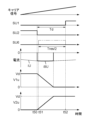
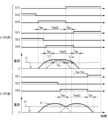
- FIG. 2 is an explanatory diagram of the operation of the control device 50 in the power conversion device 100 of the first embodiment when the control device 50 performs a basic operation when the load current is > 0 and the resonant capacitor 9 is being charged.
- the control signals SU1 and SU2 given from the control device 50 to the first switching element 1U and the second switching element 2U of the switching circuit 10U, respectively, are illustrated for the case where the first switching element of interest is the first switching element 1U of the switching circuit 10U. Also illustrated in FIG.
- the control signal SU6 given from the control device 50 to the first IGBT 6U of the switch 8U, the load current iU flowing in the U-phase of the AC load RA1, the current iL1 flowing in the resonant inductor L1, the voltage V1u across the first switching element 1U, and the voltage V2u across the second switching element 2U.
- the voltage value of the DC power source E1 is illustrated as Vd.
- FIG. 2 also shows the dead time period Td that is set in the control device 50 to prevent the first switching element 1 and the second switching element 2, which are in phase, from being turned on at the same time.
- FIG. 2 also shows the additional time Tau that is set in the control device 50 for the control signal SU6 of the first IGBT 6U of the switch 8U. The additional time Tau will be described later.
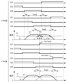
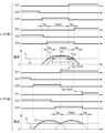
- FIG. 3 is another operation explanatory diagram when the control device 50 in the power conversion device 100 of embodiment 1 performs basic operation when the load current is > 0 and the resonant capacitor 9 is charged.
- the control signals SV1 and SV2 given from the control device 50 to the first switching element 1V and the second switching element 2V of the switching circuit 10V are illustrated. Also, FIG.
- FIG. 3 illustrates the control signal SV6 given from the control device 50 to the first IGBT 6V of the switch 8V, the load current iV flowing in the V phase of the AC load RA1, the current iL1 flowing in the resonant inductor L1, the voltage V1v across the first switching element 1V, and the voltage V2v across the second switching element 2V.
- the voltage value of the DC power source E1 is illustrated as Vd.
- FIG. 3 also shows the dead time period Td that is set in the control device 50 to prevent the first switching element 1 and the second switching element 2, which are in phase, from being turned on at the same time.
- FIG. 3 also shows the additional time Tav that is set in the control device 50 for the control signal SV6 of the first IGBT 6V of the switch 8V. The additional time Tav will be described later.
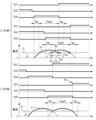
- FIG. 4 is another operation explanatory diagram when the control device 50 in the power conversion device 100 of the first embodiment performs a basic operation when the load current is >0 and the resonant capacitor 9 is being charged.
- the control signals SW1 and SW2 provided from the control device 50 to the first switching element 1W and the second switching element 2W of the switching circuit 10W are illustrated.
- the control signal SW6 provided from the control device 50 to the first IGBT 6W of the switch 8W and the load current iW flowing through the W phase of the AC load RA1 are illustrated.
- the current iL1 flowing through the resonant inductor L1 is illustrated.
- the voltage V1w across the first switching element 1W and the voltage V2w across the second switching element 2W are illustrated.
- the voltage value of the DC power source E1 is illustrated as Vd.
- FIG. 4 also illustrates the dead time period Td that is set in the control device 50 to prevent the first switching element 1W and the second switching element 2W from being turned on at the same time.
- FIG. 4 also illustrates the additional time Taw that is set in the control device 50 for the control signal SW6 of the first IGBT 6W of the switch 8W. The additional time Taw will be described later.
- the above-mentioned additional time Tau is a time set to advance the start time t1 of the high level period of the control signal SU6 to be earlier than the start time t2 of the first period, so that the high level period of the control signal SU6 is longer than the first period, as shown in FIG. 2.
- the length of the additional time Tau is set based on the value of the load current iU. In order to start LC resonance from the start time t2 of the first period, it is desirable that the value of the current iL1 matches the value of the load current iU at the start time t2 of the first period.
- the end time of the high level period of the control signal SU6 may be the same as or later than the end time t3 of the dead time period Td.
- FIG. 2 shows an example in which the end time of the high level period of the control signal SU6 is set to be the same as the end time t3 of the dead time period Td.
- the control device 50 sets the high-level period of the control signal SU6 to Tau+(Tres/2), for example. That is, the control device 50 sets the length of the first period to Tres/2.
- the voltage V2u across the second switching element 2U becomes Vd at time t3 when the dead time period Td ends, and the voltage V1u across the first switching element 1U becomes zero at time t3 when the dead time period Td ends.
- the current iL1 flowing through the resonance inductor L1 starts to flow at time t1 when the high-level period of the control signal SU6 starts, after time t0 when the dead time period Td starts, and becomes zero at time t4 when the additional time Tau has elapsed from time t3 when the dead time period Td ends.
- a detection value at the carrier period to which the additional time Tau is added, or at the timing closest to the carrier period is used.
- the estimated value of the load current iU at this time is, for example, an estimated value of the load current iU in the carrier period to which the additional time Tau is added.
- the resonance half period in the case of basic operation is half the resonance period, which is the reciprocal of the resonance frequency of the resonance circuit including the resonance inductor L1 and one resonance capacitor 9. Therefore, if the inductance of the resonance inductor L1 is L and the capacitance of the resonance capacitor 9 is C, the resonance half period is ⁇ (L ⁇ C) 1/2 .
- the length of the dead time period Td is set to be longer than the length of the resonance half period, but the length of the dead time period Td may be set to the same value as the length of the resonance half period.
- the above-mentioned additional time Tav is a time set to advance the start time t11 of the high level period of the control signal SV6 to be earlier than the start time t12 of the first period, so that the high level period of the control signal SV6 is longer than the first period, as shown in FIG. 3.
- the length of the additional time Tav is set based on the value of the load current iV. In order to start LC resonance from the start time t12 of the first period, it is desirable that the value of the current iL1 matches the value of the load current iV at the start time t12 of the first period.
- the end time of the high level period of the control signal SV6 may be the same as or later than the end time t13 of the dead time period Td.
- FIG. 3 shows an example in which the end time of the high level period of the control signal SV6 is set to be the same as the end time t13 of the dead time period Td.
- the control device 50 sets the high-level period of the control signal SV6 to Tav+(Tres/2), for example.
- the voltage V1v across the first switching element 1V becomes zero at time t13 when the dead-time period Td ends.
- the current iL1 flowing through the resonant inductor L1 starts flowing at time t11 when the high-level period of the control signal SV6 starts, after time t10 when the dead-time period Td starts, and becomes zero at time t14 when the additional time Tav has elapsed from time t13 when the dead-time period Td ends.
- the current iL1 since iL1 ⁇ iV from time t12 when the first period starts, the current iL1 in the shaded area of the current waveform in the fourth row from the top in FIG. 3 flows into the resonant capacitor 9V, and LC resonance occurs.
- the current iL1 is regenerated to the power conversion circuit 11 via the third diode 13 directly connected to the resonant inductor L1.
- the detection value at the carrier period to which the additional time Tav is added, or at the timing closest to that carrier period is used.
- the estimated value of the load current iV at this time the value estimated from the load current iV at the carrier period to which the additional time Tav is added, is used.
- the above-mentioned additional time Taw is a time set to advance the start time t21 of the high level period of the control signal SW6 to be earlier than the start time t22 of the first period, so that the high level period of the control signal SW6 is longer than the first period, as shown in FIG. 4.
- the length of the additional time Taw is set based on the value of the load current iW. In order to start LC resonance from the start time t22 of the first period, it is desirable that the value of the current iL1 matches the value of the load current iW at the start time t22 of the first period.
- the end time of the high level period of the control signal SW6 may be the same as or later than the end time t23 of the dead time period Td.
- FIG. 4 shows an example in which the end time of the high level period of the control signal SW6 is set to be the same as the end time t23 of the dead time period Td.
- the control device 50 sets the high-level period of the control signal SW6 to Taw+(Tres/2), for example.
- the voltage V1w across the first switching element 1W becomes zero at time t23 when the dead-time period Td ends.
- FIG. 4 shows an example in which the end time of the high level period of the control signal SW6 is set to be the same as the end time t23 of the dead time period Td.
- the current iL1 flowing through the resonant inductor L1 starts flowing at time t21 when the high-level period of the control signal SW6 starts, after time t20 when the dead-time period Td starts, and becomes zero at time t24 when the additional time Taw has elapsed from time t23 when the dead-time period Td ends.
- the current iL1 since iL1 ⁇ iW from time t22 when the first period starts, the current iL1 in the shaded area of the current waveform in the fourth row from the top in FIG. 4 flows into the resonant capacitor 9W, and LC resonance occurs.
- the current iL1 is regenerated to the power conversion circuit 11 via the third diode 13 directly connected to the resonant inductor L1.
- FIG. 6 is an explanatory diagram of the first current threshold I1 and the second current threshold I2 used by the control device 50 in the power conversion device 100 of the first embodiment.
- the target of the soft switching is the second switching element 2 (hereinafter also referred to as the target second switching element 2)
- the polarity of the load current (load current iU, load current iV, or load current iW) flowing through the AC terminal 41 connected to the target second switching element 2 is positive
- the control device 50 when the current value of the load current is larger than the first current threshold I1, the control device 50 does not turn on the switch 8, and when the current value of the load current is smaller than the first current threshold I1, the control device 50 turns on the switch 8 during the dead time period Td.
- the length of the dead time period Td is set to be longer than the resonance half cycle.
- the control device 50 when the current value of the load current is greater than the first current threshold I1, the control device 50 can discharge the resonance capacitor 9U connected in parallel to the target second switching element 2 by the load current iU without turning on the switch 8 corresponding to the target second switching element 2. This allows the power conversion device 100 to realize zero-voltage soft switching of the target second switching element 2.
- FIG. 7 is an explanatory diagram of the operation of the control device 50 in the power conversion device 100 of embodiment 1 when the control device 50 performs basic operation when the load current is >0 and the resonant capacitor 9 is discharging.
- FIG. 7 illustrates the control signals SU1, SU2, and SU7, the load current iU, the current i9U flowing from the resonant capacitor 9U, and the voltage V2u across the second switching element 2U when the second switching element 2 in question is the second switching element 2U of the switching circuit 10U and the current value of the load current is greater than the first current threshold I1.
- FIG. 7 also illustrates the dead time period Td and the additional time Tau set in the control device 50 for the control signal SU7 of the second IGBT 7U of the switch 8U.
- the control device 50 does not provide a high level period for the control signal SU7.
- the current i9U starts to flow from the resonant capacitor 9U, and the current i9U drops to zero before time t33 when the dead time period Td ends, and the voltage V2u across the second switching element 2U becomes zero before time t33 when the dead time period Td ends.
- the second switching element 2U is zero voltage soft switched.
- the control device 50 When the current value of the load current iU is smaller than the first current threshold I1, the control device 50 provides a high-level period for the control signal SU7, for example, as shown by the two-dot chain line in FIG. 7. At this time, the time t32 at which the high-level period of the control signal SU7 starts is, for example, later than the time t31 at which the dead time period Td starts. The time at which the high-level period of the control signal SU7 ends is the same as the time t33 at which the dead time period Td ends. As a result, in the power conversion device 100, the voltage V2u across the second switching element 2U becomes zero before the time t33 at which the dead time period Td ends.
- the second switching element 2U is zero-voltage soft-switched.
- the time at which the high-level period of the control signal SU7 starts may be time t30, which is earlier than the time at which the first period starts by an additional time Tau.
- the end time of the high level period of the control signal SU7 may be time t34 that is later than time t33 at which the dead time period Td ends by the additional time Tau.
- the time before and after the first period is not limited to the additional time Tau, and may be other set times.
- the control device 50 may set the high level period of the control signal to the switch 8 so that the switch 8 is turned on, for example, in the first period even if the current value of the load current is larger than the first current threshold I1.
- the control device 50 may not turn on the switch 8 in the first period even if the current value of the load current is smaller than the first current threshold I1.
- the control device 50 may set the high level period of the control signal to the switch 8 so that the switch 8 is always turned on, for example, in the first period, regardless of the first current threshold I1.
- control device 50 may always keep the switch 8 in the off state regardless of the first current threshold I1.
- the control device 50 may also combine the operations described in (3.1.2) as appropriate.
- the control device 50 may not match the high-level period of the control signal to the switch 8 with the first period as described above.
- the high-level period of the control signal to the switch 8 may be designed to have a length other than the first period, depending on the design time of the resonance half cycle.
- FIG. 8 is an explanatory diagram of the operation of the control device 50 in the power conversion device 100 of embodiment 1 when the control device 50 performs basic operation when the load current is ⁇ 0 and the resonant capacitor 9 is discharging.
- FIG. 8 illustrates the control signals SU1, SU2, and SU7, the load current iU, the current iL1 flowing through the resonant inductor L1, and the voltage V2u across the second switching element 2U when the second switching element 2 in question is the second switching element 2U of the switching circuit 10U.
- FIG. 8 also illustrates the dead time period Td set in the control device 50 to prevent the first switching element 1 and the second switching element 2 of the same phase from being turned on at the same time. Also, FIG. 8 illustrates the additional time Tau set in the control device 50 for the control signal SU7 of the second IGBT 7U of the switch 8U.
- the end point of the high level period of the control signal SU7 may be the same as the end point t43 of the dead time period Td or later.
- FIG. 8 illustrates an example in which the end point of the high level period of the control signal SU7 is set to the same as the end point t43 of the dead time period Td.
- the control device 50 sets the high level period of the control signal SU7 to Tau + (Tres/2).
- the voltage V2u across the second switching element 2U becomes zero at the end point t43 of the dead time period Td.
- the current iL1 flowing through the resonant inductor L1 starts at time t41 when the high level period of the control signal SU7 starts, after time t40 when the dead time period Td starts, and becomes zero at time t44 when the additional time Tau has elapsed from time t43 when the dead time period Td ends.
- the load current value at this time (the detection result of the load current iU or its signal processing value)
- a detection value at the carrier cycle to which the additional time Tau is added, or at the timing closest to the carrier cycle, etc. is used.
- an estimated value of the load current iU at this time an estimated value of the load current iU at the carrier cycle to which the additional time Tau is added, etc. is used.
- the resonance half period in the case of basic operation is half the resonance period which is the reciprocal of the resonance frequency of the resonance circuit including the resonance inductor L1 and one resonance capacitor 9. Therefore, when the inductance of the resonance inductor L1 is L and the capacitance of the resonance capacitor 9 is C, the resonance half period is ⁇ (L ⁇ C) 1/2 .
- the length of the dead time period Td in the basic operation is set to be longer than the resonance half period in the basic operation, for example, but may be set to be the same as the resonance half period in the basic operation.
- the length of the dead time period Td is set to be longer than the length of the resonant half cycle.
- the power conversion device 100 can charge the resonant capacitor 9U connected in series to the target first switching element 1 with the load current without the control device 50 turning on the switch 8 corresponding to the target first switching element 1. This allows the power conversion device 100 to realize zero-voltage soft switching of the target first switching element 1.
- FIG. 9 is an explanatory diagram of the operation of the control device 50 in the power conversion device 100 of embodiment 1 when the control device 50 performs basic operation when the load current is ⁇ 0 and the resonant capacitor 9 is charging.
- FIG. 9 illustrates the control signals SU1, SU2, and SU6, the load current iU, the current i9U flowing from the resonant capacitor 9U, and the voltage V2u across the second switching element 2U when the first switching element 1 under consideration is the first switching element 1U of the switching circuit 10U and the current value of the load current is greater than the second current threshold I2 (in other words, when the absolute value of the current value of the load current is less than the absolute value of the second current threshold I2).
- FIG. 9 also illustrates the dead time period Td.
- the control device 50 When the current value of the load current is smaller than the second current threshold I2 (in other words, when the absolute value of the load current is greater than the absolute value of the second current threshold I2), the control device 50 does not provide a high level period for the control signal SU6. In this case, in the power conversion device 100, the current i9U starts to flow through the resonant capacitor 9U from time t50 when the control signal SU2 changes from high level to low level.
- the resonant capacitor 9U is charged and the voltage V2u across the second switching element 2U increases, the current i9U becomes zero before time t52 when the dead time period Td ends, and the voltage V1u across the first switching element 1U becomes zero before time t52 when the dead time period Td ends.
- the first switching element 1U is zero-voltage soft-switched when the control signal SU1 changes from low level to high level at time t52 when the dead time period Td ends.
- the control device 50 When the current value of the load current is greater than the second current threshold I2 (in other words, when the absolute value of the load current is less than the absolute value of the second current threshold), the control device 50 provides a high level period for the control signal SU6, for example as shown by the two-dot chain line in FIG. 9.
- the time point at which the high level period of the control signal SU6 starts is time point t51, which is later than time point t50 at which the dead time period Td starts.
- the time point at which the high level period of the control signal SU6 ends is the same as time point t52 at which the dead time period Td ends.
- the voltage V1u across the first switching element 1U becomes zero before time point t52 at which the dead time period Td ends. Therefore, in the power conversion device 100, when the control signal SU1 changes from low level to high level at time point t52 at which the dead time period Td ends, the first switching element 1U is zero-voltage soft-switched. Moreover, the relationship between the threshold value of the load current and the method of determining the high-level period of the control signal to the switch 8 described above is an ideal design example, and is not limited to the above design example.
- control device 50 may set the high-level period of the control signal to the switch 8 so that the switch 8 is turned on, for example, in the first period, even if the current value of the load current is smaller than the second current threshold I2. Furthermore, the control device 50 may not turn on the switch 8 in the first period, even if the current value of the load current is larger than the second current threshold I2. Furthermore, the control device 50 may set the high-level period of the control signal to the switch 8 so that the switch 8 is always turned on, for example, in the first period, regardless of the second current threshold I2. Furthermore, the control device 50 may always keep the switch 8 in the off state, regardless of the second current threshold I2. Furthermore, the control device 50 may appropriately combine the operations described in (3.1.4).
- control device 50 may not match the high-level period of the control signal to the switch 8 with the first period as described above. For example, depending on the design time of the resonance half cycle, the control device 50 may set the high-level period of the control signal to the switch 8 to a length other than the first period.
- control device 50 determines that a resonant current passing through each of two or more switches 8 of the multiple switches 8 flows simultaneously in the resonant inductor L1
- the control device 50 performs one of the first control operation and the second control operation.
- the control device 50 is configured to perform one of the first control operation and the second control operation based on an overlap period Tov (see FIGS. 12 and 14 ) during which a resonant current passing through each of the two or more switches 8 flows simultaneously.
- the first control operation is an operation for shifting the high-level period of the control signal to at least one of the two or more switches 8 so that the resonant currents passing through each of the two or more switches 8 do not flow simultaneously through the resonant inductor L1.
- the second control operation is an operation of shifting the high-level period of the control signal to at least one of the two or more switches 8 so that the high-level period of the control signal to each of the two or more switches 8 overlaps for a predetermined period or more in the dead time period corresponding to each of the two or more switching circuits 10 connected to the two or more switches 8 among the multiple switching circuits 10.
- the predetermined period is, for example, the entire period of the resonance half cycle of the resonance circuit including the resonance inductor L1 and the two or more resonance capacitors 9 connected to each of the two or more switches 8.
- the control device 50 can execute a third control operation of making the high-level period of the control signal to each of the two or more switches 8 longer than the predetermined period by an additional time. The control device 50 executes the third control operation when executing the second control operation.
- FIG. 5 is a diagram showing the time change of the duty corresponding to each voltage command of three phases and the time change of the load current in an AC load connected to a plurality of AC terminals of the power conversion device 100 of the first embodiment.
- the phases of the voltage commands of the three phases (U phase, V phase, and W phase) differ from each other by 120°, but the command values of the voltage commands of two phases approach each other at an electrical angle of 60°, and the duties of the control signals of the two phases approach each other (see the first area A1 and the second area A2 in FIG. 5).
- the duty of the control signal of the U phase and the duty of the control signal of the V phase are around 0.75.
- the duty of the control signal of the U phase and the duty of the control signal of the V phase are around 0.25.
- the polarity of the resonant current is the same as the polarity of the current iL1, and in the first region A1, the polarity of the resonant current is positive, and in the second region A2, the polarity of the resonant current is negative.
- the time difference between the time t1 see FIG.
- the U-phase resonant current and the V-phase resonant current may flow simultaneously through the resonant inductor L1.
- the direction of the resonant current is opposite to that in the case of the first region A1, but the U-phase resonant current and the V-phase resonant current may flow simultaneously through the resonant inductor L1.
- each of the multiple resonant capacitors 9U, 9V, and 9W is C
- the resonant frequency of the resonant circuit including the resonant inductor L1 will change compared to when a single-phase current flows through the resonant inductor L1, and zero-voltage soft switching may not be achieved.
- FIG. 10 is a timing chart for explaining an example of a boundary condition in the case where the currents flowing through the resonance inductor L1 do not overlap (do not flow simultaneously) and overlap (flow simultaneously) in the power conversion device 100 of the first embodiment.
- FIG. 10 is a diagram showing an example of a boundary condition in the case where the U-phase current (current passing through the switch 8U) and the V-phase current (current passing through the switch 8V) do not overlap (do not flow simultaneously) and overlap (flow simultaneously) in the resonance inductor L1. The boundary condition will be described with reference to FIG. 10.
- FIG. 10 is a diagram showing an example of a boundary condition in the case where the U-phase current (current passing through the switch 8U) and the V-phase current (current passing through the switch 8V) do not overlap (do not flow simultaneously) and overlap (flow simultaneously) in the resonance inductor L1. The boundary condition will be described with reference to FIG. 10.
- FIG. 10 is a diagram showing an example of a boundary condition in the case where the
- 11 is a timing chart for explaining an example of a boundary condition in the case where the U-phase resonant current and the V-phase resonant current do not overlap (do not flow simultaneously) and overlap (flow simultaneously) in the power conversion device 100 of the first embodiment.
- 11 is a diagram showing an example of boundary conditions between a case where the U-phase resonant current and the V-phase resonant current do not overlap (do not flow simultaneously) in the resonant inductor L1 and a case where they overlap (flow simultaneously). The boundary conditions will be described with reference to FIG.
- the U-phase current and the V-phase current do not overlap in the resonant inductor L1
- the time difference ⁇ Tuv is less than Tau+Tav+(Tres/2)
- the U-phase current and the V-phase current overlap.
- the time difference ⁇ Tuv is the time difference between time t3 when the high-level period of the control signal SU1 starts and time t13 when the high-level period of the control signal SV1 starts.
- the U-phase resonant current and the V-phase resonant current do not overlap in the resonant inductor L1
- the time difference ⁇ Tuv is less than Tres/2
- the U-phase resonant current and the V-phase resonant current overlap in the resonant inductor L1.
- the control device 50 sets the threshold value for the time difference ⁇ Tuv to Tres/2. If the time difference ⁇ Tuv is less than Tres/2, the control device 50 estimates that resonant currents corresponding to two phases of the switching circuits 10, switching circuit 10U and switching circuit 10V, among the multiple switching circuits 10, flow simultaneously through the resonant inductor L1.
- the above threshold value setting is one example, and may be set to another value. For example, taking into account an error in the value of Tres/2, the threshold value may be set to a value even larger than Tres/2.
- the method of calculating the time difference ⁇ Tuv used to determine whether the resonant currents of the two phases flow simultaneously is not limited to the above example, and other calculation methods may be used as long as they can calculate a time difference equivalent to the time difference ⁇ Tuv.
- the time difference ⁇ Tuv used to determine whether two-phase resonant currents flow simultaneously may be the time difference between the end point t0 of the high-level period of the control signal SU2 (see FIG. 2) and the end point t10 of the high-level period of the control signal SV2 (see FIG. 3).
- the time difference between time t3 (see FIG. 2) when the high-level period of the control signal SU1 starts and time t23 (see FIG. 4) when the high-level period of the control signal SW1 starts is referred to as ⁇ Tuw.
- the time difference ⁇ Tuw is Tres/2 or more, the U-phase resonant current and the W-phase resonant current do not overlap in the resonant inductor L1, and if the time difference ⁇ Tuw is less than Tres/2, the U-phase resonant current and the W-phase resonant current overlap in the resonant inductor L1.
- the control device 50 sets a threshold value for the time difference ⁇ Tuw to Tres/2. If the time difference ⁇ Tuw is less than the threshold value, the control device 50 estimates that the resonant currents corresponding to the two phases of the switching circuits 10U and 10W among the multiple switching circuits 10 flow simultaneously through the resonant inductor L1.
- the above threshold value is an example, and may be set to another value. For example, the threshold value may be set to a value even larger than Tres/2, taking into account an error in the value of Tres/2.
- the calculation method of the time difference ⁇ Tuw used to determine whether the resonant currents of the two phases flow simultaneously is not limited to the above example, and other calculation methods may be used as long as they can calculate a time difference equivalent to the time difference ⁇ Tuw.
- the time difference ⁇ Tuw used to determine whether the resonant currents of the two phases flow simultaneously may be the time difference between the time t0 (see FIG. 2) at which the high-level period of the control signal SU2 ends and the time t20 (see FIG. 4) at which the high-level period of the control signal SW2 ends.
- time difference between time t13 (see FIG. 3) at which the high-level period of the control signal SV1 given to the first switching element 1V of the switching circuit 10V starts, and time t23 (see FIG. 4) at which the high-level period of the control signal SW1 given to the first switching element 1W of the switching circuit 10W starts is described as ⁇ Tvw.
- the V-phase resonant current and the W-phase resonant current do not overlap in the resonant inductor L1
- the time difference ⁇ Tvw is less than Tres/2
- the V-phase resonant current and the W-phase resonant current overlap in the resonant inductor L1.
- the control device 50 sets a threshold value for the time difference ⁇ Tvw to Tres/2. If the time difference ⁇ Tvw is less than the threshold value, the control device 50 estimates that resonant currents corresponding to two phases, switching circuit 10V and switching circuit 10W, among the multiple switching circuits 10, flow simultaneously through the resonant inductor L1.
- the above threshold value is an example, and may be set to another value. For example, taking into account an error in the value of Tres/2, the threshold value may be set to a value even larger than Tres/2.
- the method of calculating the time difference ⁇ Tvw used to determine whether the resonant currents of the two phases flow simultaneously is not limited to the above example, and other calculation methods may be used as long as they can calculate a time difference equivalent to the time difference ⁇ Tvw.
- the time difference ⁇ Tvw used to determine whether two-phase resonant currents flow simultaneously may be the time difference between time t10 (see FIG. 3) at which the high-level period of the control signal SV2 ends and time t20 (see FIG. 4) at which the high-level period of the control signal SW2 ends.
- control device 50 can determine whether two-phase resonant currents flow simultaneously using the same time difference and threshold value as in the case of charging operation of the resonant capacitor 9.
- the control device 50 estimates that the U-phase resonant current and the V-phase resonant current overlap.
- a threshold value e.g., Tres/2
- the control device 50 estimates that the U-phase resonant current and the W-phase resonant current overlap.
- a threshold value e.g., Tres/2
- the control device 50 estimates that the V-phase resonant current and the W-phase resonant current overlap.
- a threshold value e.g., Tres/2
- the control device 50 shifts the high-level period of the control signal to one of the two switches 8 so that the resonant currents passing through each of the two switches 8 do not flow simultaneously through the resonant inductor L1.
- the control device 50 performs the first control operation so that the length of the dead time period Td between the high-level period of the control signal provided to the first switching element 1 and the high-level period of the control signal provided to the second switching element 2 of the two switching circuits 10 corresponding to the two switches 8 does not change.
- the control device 50 shifts the high-level period of the control signal to one of the two switches 8 so that the high-level period of the control signal to each of the two switches 8 overlaps for a predetermined period or more in the dead-time period Td corresponding to each of the two switching circuits 10 connected to the two switches 8 of the multiple (three) switching circuits 10.
- the control device 50 performs the second control operation so that the length of the dead-time period Td between the high-level period of the control signal provided to the first switching element 1 and the high-level period of the control signal provided to the second switching element 2 of the two switching circuits 10 corresponding to the two switches 8 does not change.
- the shift time of the high level period of the control signal SU6 or SU7 to the switch 8U when the high level period of the control signal SU6 or SU7 is shifted is defined as Tsu.
- the shift time of the high level period of the control signal SV6 or SV7 to the switch 8V when the high level period of the control signal SV6 or SV7 is shifted is defined as Tsv.
- the shift time of the high level period of the control signal SW6 or SW7 to the switch 8W when the high level period of the control signal SW6 or SW7 is shifted is defined as Tws.
- FIG. 12 is a timing chart for explaining the operation when the control device 50 performs the first control operation in the power conversion device 100 of the first embodiment.
- the upper part of FIG. 12 illustrates a timing chart in the case where the control device 50 determines in advance that two-phase resonant currents of the U phase and the V phase flow simultaneously in the period corresponding to the first region A1 of FIG. 5.
- the upper part of FIG. 12 illustrates a timing chart of the control signals SU1, SU2, SV1, SV2, the control signals SU6, SV6, the load currents iU, iV, and the current iL1 before the shift.
- FIG. 12 illustrates a timing chart for explaining the operation when the control device 50 performs the first control operation in the power conversion device 100 of the first embodiment.
- the upper part of FIG. 12 illustrates a timing chart in the case where the control device 50 determines in advance that two-phase resonant currents of the U phase and the V phase flow simultaneously in the period corresponding to the first region A1
- the length of the overlap period Tov in which the resonant current (resonant current of the U phase) passing through the switch 8U and the resonant current (resonant current of the V phase) passing through the switch 8V flow simultaneously is shorter than the length of the time difference ⁇ Tuv.
- the lower part of FIG. 12 shows a timing chart when the control device 50 performs the first control operation (hereinafter also referred to as after the shift).
- the lower part of FIG. 12 shows timing charts of the control signals SV1, SV2, control signal SV6, load currents iU, iV, and current iL1 after the shift.
- the polarity of the load currents iU, iV flowing through the two AC terminals 41U, 41V connected to the two switches 8U, 8V is positive
- the absolute value of the load current iU is the same as the absolute value of the load current iV.
- FIG. 12 shows a timing chart for one period of the carrier signal.
- the control device 50 when the control device 50 performs the first control operation, it shifts the high-level period of the control signal SV6 by a shift time Tsv in the direction of delaying the high-level period.
- the length of the shift time Tsv is the same as the length of the overlap period Tov during which the resonant current (U-phase resonant current) passing through the switch 8U and the resonant current (V-phase resonant current) passing through the switch 8V flow simultaneously.
- Tov Tres/2- ⁇ Tuv. Therefore, as shown in the lower part of FIG. 12, the resonant current passing through the switch 8U and the resonant current passing through the switch 8V do not overlap, making it possible to perform zero-voltage soft switching of the first switching element 1U.
- FIG. 13 is a waveform diagram of the load current in the power conversion device 100 of embodiment 1.
- the shift time Tsv can be shortened compared to when the control device 50 shifts the high-level period of the control signal SV6 by the shift time Tsv in the direction of advancing the period when the condition Tov ⁇ Tuv is satisfied, and the current distortion of the output current iV within one period of the carrier signal (see FIG. 13) is reduced. Note that one period of the carrier signal is shorter than one period of the output current iV and shorter than half the period of the output current iV.
- FIG. 14 is a timing chart for explaining the operation of the control device 50 in the power conversion device 100 of the first embodiment when the control device 50 performs the second control operation.
- the upper part of FIG. 14 illustrates a timing chart in the case where the control device 50 has determined in advance that two-phase resonant currents, U-phase and V-phase, flow simultaneously in the period corresponding to the first region A1 of FIG. 5.
- the upper part of FIG. 14 illustrates timing charts of the control signals SU1, SU2, SV1, SV2, control signals SU6, SV6, load currents iU, iV, and current iL1 before the shift.
- FIG. 14 illustrates timing charts of the control signals SU1, SU2, SV1, SV2, control signals SU6, SV6, load currents iU, iV, and current iL1 before the shift.
- the length of the overlap period Tov during which the resonant current (U-phase resonant current) passing through the switch 8U and the resonant current (V-phase resonant current) passing through the switch 8V flow simultaneously is longer than the length of the time difference ⁇ Tuv.
- the lower part of FIG. 14 shows a timing chart when the control device 50 performs the second control operation (hereinafter also referred to as after the shift).
- the lower part of FIG. 14 shows timing charts of the control signals SV1, SV2, control signal SV6, load currents iU, iV, and current iL1 after the shift.
- the polarity of the load currents iU, iV flowing through the two AC terminals 41U, 41V connected to the two switches 8U, 8V is positive
- the absolute value of the load current iU is the same as the absolute value of the load current iV.
- FIG. 14 shows a timing chart for one period of the carrier signal.
- control device 50 executes the first step, the second step, and the third step in the order of the first step, the second step, and the third step.
- the U-phase control signals SU1, SU2 are synchronized with the V-phase control signals SV1, SV2.
- the start point of the high-level period of the V-phase control signal SV1 and the end point of the high-level period of the V-phase control signal SV2 are shifted forward by a shift time Tsv in the example in the upper part of FIG. 14, thereby synchronizing the U-phase control signals SU1, SU2 with the V-phase control signals SV1, SV2.
- Tsv shift time
- the shift time Tsv is the time difference ⁇ Tuv between the start point of the high-level period of the control signal SU1 before the shift and the start point of the high-level period of the control signal SV1.
- the time difference ⁇ Tuv may be the time difference between the end point of the high-level period of the control signal SU2 and the end point of the control signal SV2.
- the high-level periods of the U-phase control signals SU1 and SU2 may be shifted in a direction to delay the high-level periods by the shift time Tsu, thereby synchronizing the U-phase control signals SU1 and SU2 with the V-phase control signals SV1 and SV2.
- of the total current of the load currents iU and iV of the two phases is added to the high level period of the control signals SU6 and SV6 to the switches 8 of the two phases corresponding to the resonant half cycle Tres/2 of each of the two phases.
- the second step corresponds to the third control operation described above.
- the control device 50 sets the length of the period obtained by subtracting the additional time Tad from the high level period of each of the control signals SU6 and SV6 to 2 1/2 ⁇ Tres/2, which is the resonant half cycle of the resonant circuit, and changes the dead time period to a dead time period longer than the resonant half cycle of the resonant circuit.
- the end point of the high level period of the control signals SU6 and SV6 may be any time after the end point of the resonant half cycle.
- the control device 50 when the control device 50 does not execute the second control operation, the voltages V2u and V2v across the second switching elements 2U and 2V do not rise to Vd at the time when the control signals SU1 and SV1 change from a low level period to a high level period (the end of the dead time period corresponding to the U phase and the V phase, respectively).
- the control device 50 when the control device 50 does not execute the second control operation, the charging of the resonance capacitors 9U and 9V does not end at the end of the dead time period Td corresponding to the U phase and the V phase, respectively.
- the voltages across the first switching elements 1U and 1V do not decrease to zero at the end of the dead time period corresponding to the U phase and the V phase, respectively.
- the switching of the first switching elements 1U and 1V becomes hard switching.
- the control device 50 executes the second control operation
- the voltages V2u, V2v across the second switching elements 2U, 2V rise to Vd at the point when the control signals SU1, SV1 change from a low level period to a high level period (the end point of the dead time period corresponding to the U phase and the V phase, respectively).
- the control device 50 executes the second control operation
- the charging of the resonant capacitors 9U, 9V ends at the end point of the dead time period corresponding to the U phase and the V phase, respectively.
- the switching of the first switching elements 1U, 1V becomes zero voltage soft switching.
- the start point of the high-level period of the control signal SV1 may be earlier than the start point of the high-level period of the control signal SU1
- the start point of the high-level period of the control signal SV6 may be earlier than the start point of the high-level period of the control signal SU6.
- control device 50 when the control device 50 performs the second control operation, it shifts the high-level period of the control signal SV6 forward by the shift time Tsv.
- the length of the shift time Tsv is the same as the length of the time difference ⁇ Tuv.
- the shift time Tsv can be made shorter than when the control device 50 shifts the high-level period of the control signal SV6 in a direction to delay the high-level period by the length of the overlap period Tov when the condition Tov> ⁇ Tuv is satisfied, and the current distortion of the output current iV within one period of the carrier signal (see FIG. 13) is reduced.
- the control device 50 performs a first control operation when the length of the overlap period Tov is shorter than the length of the time difference ⁇ Tuv, and performs a second control operation when the length of the overlap period Tov is longer than the length of the time difference ⁇ Tuv.
- the voltages V2u and V2v across the second switching elements 2U and 2V do not decrease to zero at the time when the control signals SU2 and SV2 change from a low level period to a high level period (the end of the dead time period Td corresponding to the U phase and the V phase, respectively).
- the discharge of the resonance capacitors 9U and 9V does not end at the end of the dead time period Td corresponding to the U phase and the V phase, respectively.
- the control device 50 does not perform either the first control operation or the second control operation, the voltages across the second switching elements 2U and 2V do not decrease to zero at the end of the dead time period Td corresponding to the U phase and the V phase, respectively.
- the switching of the second switching elements 2U and 2V becomes hard switching.
- the voltages V2u, V2v across the second switching elements 2U, 2V decrease to zero at the point when the control signals SU2, SV2 change from a low level period to a high level period (the end point of the dead time period Td corresponding to the U phase and the V phase, respectively).
- the discharge of the resonance capacitors 9U, 9V ends at the end of the dead time period Td corresponding to the U phase and the V phase, respectively.
- the switching of the second switching elements 2U, 2V becomes zero voltage soft switching.
- the control device 50 determines that a resonant current flows simultaneously through three of the multiple switches 8 in the resonant inductor L1, it performs either a first control operation or a second control operation on two switches 8 with the same load current polarity based on the overlap period Tov. Furthermore, it stops the operation of the switch 8 corresponding to the one-phase AC terminal 41 with the different load current polarity (the high level period of the control signal within one carrier period is set to zero). "When it is determined that a resonant current flows simultaneously through three of the multiple switches 8" means that it has been estimated in advance that a resonant current flows simultaneously through the resonant inductor L1 through each of the three switches 8.
- the control device 50 determines that three-phase resonant currents flow simultaneously when, for example, the time difference between the start point of the high-level period of the control signal SU6 corresponding to the U phase and the start point of the high-level period of the control signal SV6 corresponding to the V phase, the time difference between the start point of the high-level period of the control signal SV6 corresponding to the V phase and the start point of the high-level period of the control signal SW6 corresponding to the W phase, and the time difference between the start point of the high-level period of the control signal SW6 corresponding to the W phase and the start point of the high-level period of the control signal SU6 corresponding to the U phase are all less than a threshold value.
- each of the multiple resonant capacitors 9U, 9V, and 9W is C
- the resonant frequency of the resonant circuit including resonant inductor L1 will change compared to when one-phase current flows through resonant inductor L1, and zero-voltage soft switching may not be achieved.
- the control device 50 determines in advance that three-phase resonant currents of the U, V, and W phases will flow simultaneously, it performs the first control operation or the second control operation, thereby realizing soft switching of the two target switching elements corresponding to the two switches 8 while reducing the current distortion of the load current (output current) flowing through the AC terminal 41 of one of the two switches 8.
- control device 50 also performs either the first control operation or the second control operation for the two switches 8 having the same load current polarity based on the overlap period Tov, and further stops the operation of the switch 8 corresponding to the AC terminal 41 of one phase having a different load current polarity.
- the control device 50 performs one of a first control operation and a second control operation based on an overlap period Tov during which the resonant currents passing through the two or more switches 8 flow simultaneously.
- the first control operation shifts a high-level period of a control signal to at least one of the two or more switches 8 so that the resonant currents passing through the two or more switches 8 do not flow simultaneously through the resonant inductor L1.
- the second control operation shifts a high-level period of a control signal to at least one of the two or more switches 8 so that the high-level periods of the control signal to the two or more switches 8 overlap by a predetermined period or more in a dead time period corresponding to each of the two or more switching circuits 10 connected to the two or more switches 8 among the multiple switching circuits 10.
- the above configuration makes it possible to reduce current distortion. More specifically, the above configuration makes it possible for the control device 50 to perform one of the first and second control operations based on the overlap period Tov during which the resonant currents flow simultaneously through two or more switches 8, thereby realizing soft switching while reducing current distortion in the load current (output current).
- the first switching element 1 or the second switching element 2 that is the target of zero voltage soft switching in one of the two or more switching circuits 10 is set as the first target switching element.
- the first switching element 1 or the second switching element 2 that is the target of zero voltage soft switching in one of the two or more switching circuits 10 that is different from the switching circuit 10 that includes the first target switching element is set as the second target switching element.
- the time difference between the start of the high level period of the control signal to the first target switching element and the start of the high level period of the control signal to the second target switching element is set as ⁇ T.
- control device 50 performs the first control operation when the length of the overlap period Tov of the resonant current is less than ⁇ T, and performs the second control operation when the length of the overlap period Tov of the resonant current is equal to or greater than ⁇ T.
- the above configuration makes it possible to reduce the amount of shift during which the control signal is at a high level, thereby reducing current distortion.
- one of the two or more switches 8 is designated as a first switch, and the other switch is designated as a second switch.
- the control device 50 shifts the high-level period of the control signal to one of the first switch and the second switch so that the resonant current flows through the second switch from the point in time when the current value of the resonant current passing through the first switch becomes an extreme value and coincides with the current value of the load current flowing through the AC terminal 41 corresponding to the first switch among the two or more AC terminals 41.
- the above configuration reduces the amount of shift during the high-level period of the control signal, making it possible to achieve higher frequencies.
- Embodiment 2 (1) Circuit Configuration of Power Conversion Device
- the circuit configuration of the power conversion device 100 according to the second embodiment is the same as that of the power conversion device 100 according to the first embodiment (see FIG. 1 ), and therefore will not be illustrated or described.
- FIG. 15 is a timing chart for explaining the operation when the control device 50 performs the first control operation in the power conversion device 100 according to the second embodiment.
- Fig. 16 is a timing chart for explaining the operation when the control device 50 performs the second control operation in the power conversion device 100 of the second embodiment.
- Figs. 15 and 16 can be viewed in the same way as Figs. 12 and 14, respectively, and therefore will not be described.
- the control device 50 performs the first control operation when the length of the overlap period Tov is shorter than the length of the time difference ⁇ Tuv. In the example of FIG. 15, the length of the time difference ⁇ Tuv is longer than the length of the overlap period Tov.
- the control device 50 shifts the high level period of the control signal SU6 and the high level period of the control signal SV6 in opposite directions. In the example of FIG. 15, the control device 50 shifts the end point of the high level period of the control signal SU6 by the shift time Tsu in the direction of advancing, and shifts the end point of the high level period of the control signal SV6 by the shift time Tsv in the direction of delaying.
- the control device 50 shifts the start point of the high level period of the control signal SU1 by the shift time Tsu in the direction of advancing. Also, the control device 50 shifts the start point of the high level period of the control signal SV1 by the shift time Tsv in the direction of delaying.
- the length of the shift time Tsu is the same as the length of Tov/2. Additionally, the length of the shift time Tsv is the same as the length of Tov/2.
- the control device 50 performs the first control operation, eliminating the overlap period Tov between the U-phase resonant current and the V-phase resonant current as shown in FIG. 15, and enabling zero-voltage soft switching of the first switching elements 1U and 1V.
- control device 50 performs the second control operation.
- the length of the time difference ⁇ Tuv is shorter than the length of the overlap period Tov.
- the control device 50 shifts the high-level period of the control signal SU6 and the high-level period of the control signal SV6 in opposite directions.
- the control device 50 shifts the end point of the high-level period of the control signal SU6 by the shift time Tsu in a direction to delay the end point, and shifts the end point of the high-level period of the control signal SV6 by the shift time Tsv in a direction to advance the end point.
- the control device 50 shifts the start point of the high-level period of the control signal SU1 by the shift time Tsu in a direction to delay the end point.
- the control device 50 also shifts the start point of the high-level period of the control signal SV1 by the shift time Tsv in a direction to advance the end point.
- the length of the shift time Tsu is the same as the length of ⁇ Tuv/2.
- the length of the shift time Tsv is the same as the length of ⁇ Tuv/2.
- the control device 50 performs the second control operation, which enables zero-voltage soft switching of the first switching elements 1U and 1V, similar to the case where the control device 50 performs the second control operation in the power conversion device 100 according to the first embodiment.
- the control device 50 performs either the first control operation or the second control operation, and the discharge of the resonant capacitors 9U and 9V ends at the end of the dead time period corresponding to the U phase and the V phase, respectively. Therefore, in the power conversion device 100, when the control device 50 performs the first control operation or the second control operation, the switching of the second switching elements 2U and 2V becomes zero voltage soft switching.
- the control device 50 performs one of the first control operation and the second control operation based on the overlap period Tov during which resonant currents flow simultaneously through two or more switches 8, respectively. This makes it possible to reduce current distortion.
- the power conversion device 100 shifts the high-level periods of the control signals to the two switches 8 in opposite directions, and makes the length of the shift time of the high-level periods of the two control signals the same. This makes it possible to reduce current distortion and variation in the load current of each phase compared to the first embodiment.
- the power conversion device 100 shifts the high-level periods of the control signals to the two switches 8 in opposite directions, and sets the lengths of the shift times of the high-level periods of the two control signals to the same length. This makes it possible to reduce current distortion and variation in the load current of each phase compared to the first embodiment.
- FIG. 17 is a timing chart for explaining the operation when the control device 50 performs the first control operation in the power conversion device 100 according to the third embodiment.
- Fig. 18 is a timing chart for explaining the operation when the control device 50 performs the second control operation in the power conversion device 100 of the third embodiment.
- Figs. 17 and 18 can be viewed in the same way as Figs. 12 and 14, respectively, and therefore will not be described.
- the control device 50 performs the first control operation when the length of the overlap period Tov is shorter than the length of the time difference ⁇ Tuv. In the example of FIG. 17, the length of the time difference ⁇ Tuv is longer than the length of the overlap period Tov.
- the control device 50 shifts the high level period of the control signal SU6 and the high level period of the control signal SV6 in opposite directions. In the example of FIG. 17, the control device 50 shifts the end point of the high level period of the control signal SU6 by the shift time Tsu in the direction of advancing, and shifts the end point of the high level period of the control signal SV6 by the shift time Tsv in the direction of delaying.
- the control device 50 shifts the start point of the high level period of the control signal SU1 by the shift time Tsu in the direction of advancing.
- the control device 50 also shifts the start point of the high level period of the control signal SV1 by the shift time Tsv in the direction of delaying.
- the length of the shift time Tsv is the same as the length of Tov ⁇ Ta/(Ta+Tb).
- Each of Ta and Tb can be set to any value.
- the control device 50 performs the first control operation, so that the overlap period Tov between the U-phase resonant current and the V-phase resonant current before the shift is eliminated, as shown in the waveform of the current iL1 after the shift shown in the lower part of FIG. 17, and zero-voltage soft switching of the first switching elements 1U and 1V becomes possible.
- control device 50 performs the second control operation.
- the length of the time difference ⁇ Tuv is shorter than the length of the overlap period Tov.
- the control device 50 shifts the high level period of the control signal SU6 and the high level period of the control signal SV6 in opposite directions.
- the control device 50 shifts the end point of the high level period of the control signal SU6, which has an earlier phase of its high level period, by a shift time Tsu in a direction to delay the end point of the high level period of the control signal SU6, which has an earlier phase of its high level period, by a shift time Tsv in a direction to advance the end point of the high level period of the control signal SV6, which has a later phase of its high level period.
- the control device 50 shifts the start point of the high level period of the control signal SU1 by the shift time Tsu in a direction to delay the start point of the high level period.
- the control device 50 also shifts the start point of the high level period of the control signal SV1 by the shift time Tsv in a direction to advance the start point of the high level period.
- the length of the shift time Tsu is ( ⁇ 2/4) Tres - Tov Tb/(Ta + Tb).
- the length of the shift time Tsv is Tov Tb/(Ta + Tb) + ⁇ Tuv - ( ⁇ 2/4) Tres.
- the control device 50 performs the second control operation, thereby enabling zero-voltage soft switching of the first switching elements 1U and 1V, similar to the case where the control device 50 performs the second control operation in the power conversion device 100 according to the first embodiment.
- the control device 50 performs either the first control operation or the second control operation, and the discharge of the resonant capacitors 9U and 9V ends at the end of the dead time period corresponding to the U phase and the V phase, respectively. Therefore, in the power conversion device 100, when the control device 50 performs the first control operation or the second control operation, the switching of the second switching elements 2U and 2V becomes zero voltage soft switching.
- the control device 50 performs one of the first control operation and the second control operation based on the overlap period Tov during which resonant currents flow simultaneously through two or more switches 8, respectively, and therefore it is possible to reduce current distortion.
- the control device 50 when the control device 50 performs the first control operation, the high-level periods of the control signals to the two switches 8 are shifted in opposite directions, so that, compared to the first embodiment, current distortion in the load current of each phase can be reduced, and the variation can be reduced.
- the control device 50 when the control device 50 performs the second control operation, the high-level periods of the control signals to the two switches 8 are shifted in opposite directions, so that, compared to the first embodiment, current distortion in the load current of each phase can be reduced, and the variation can be reduced.
- FIG. 19 is a circuit diagram of a system including the power conversion device 100A according to the fourth embodiment.
- components similar to those of the power conversion device 100 according to the first embodiment are denoted by the same reference numerals and will not be described.
- the first IGBT 6 and the second IGBT 7 are connected in anti-series in each of the multiple switches 8.
- the collector terminal of the first IGBT 6 and the collector terminal of the second IGBT 7 are connected in each of the multiple switches 8, the emitter terminal of the first IGBT 6 is connected to the connection point 3 of a corresponding one of the multiple switching circuits 10, and the emitter terminal of the second IGBT 7 is connected to the common connection point 25.
- Each of the multiple switches 8 further includes a diode 61 connected in anti-parallel to the first IGBT 6 and a diode 71 connected in anti-parallel to the second IGBT 7.
- each of the first IGBT 6 and the second IGBT 7 may be replaced with a MOSFET (Metal Oxide Semiconductor Field Effect Transistor) or a bipolar transistor.
- MOSFET Metal Oxide Semiconductor Field Effect Transistor
- the diodes 61 and 71 in FIG. 19 may be replaced with a parasitic diode of the replaced element, or an element built into a single chip of the replaced element.
- the diodes 61 and 71 are not limited to being external to the first IGBT 6 and the second IGBT 7, but may be elements built into a single chip.
- control device 50 is, for example, the same as the operation of the control device 50 in embodiment 1, but is not limited thereto, and may be the same as the operation of the control device 50 in embodiment 2 or embodiment 3, or these operations may be combined as appropriate.
- the power conversion device 100A according to the fourth embodiment is capable of reducing current distortion, similar to the power conversion device 100 according to the first embodiment.
- FIG. 20 is a circuit diagram of a system including the power conversion device 100B according to the fifth embodiment.
- components similar to those of the power conversion device 100 according to the first embodiment are denoted by the same reference numerals and will not be described.
- the first IGBT 6 and the second IGBT 7 are connected in anti-series in each of the multiple switches 8.
- the emitter terminal of the first IGBT 6 and the emitter terminal of the second IGBT 7 are connected in each of the multiple switches 8, the collector terminal of the second IGBT 7 is connected to the connection point 3 of a corresponding one of the multiple switching circuits 10, and the collector terminal of the first IGBT 6 is connected to the common connection point 25.
- Each of the multiple switches 8 further includes a diode 61 connected in anti-parallel to the first IGBT 6 and a diode 71 connected in anti-parallel to the second IGBT 7.
- each of the first IGBT 6 and the second IGBT 7 may be replaced with a MOSFET or a bipolar transistor.
- the diodes 61 and 71 in FIG. 20 may be replaced with a parasitic diode of the replaced element, or an element built into the chip of the replaced element.
- the diodes 61 and 71 are not limited to being externally attached to the first IGBT 6 and the second IGBT 7, but may also be elements built into the chip.
- control device 50 is, for example, the same as the operation of the control device 50 in embodiment 1, but is not limited thereto, and may be the same as the operation of the control device 50 in embodiment 2 or embodiment 3.
- the power conversion device 100B according to the fifth embodiment is capable of reducing current distortion, similar to the power conversion device 100 according to the first embodiment.
- FIG. 21 is a circuit diagram of a system including the power conversion device 100C according to the sixth embodiment.
- components similar to those of the power conversion device 100 according to the first embodiment are denoted by the same reference numerals and will not be described.
- the first MOSFET 6A and the second MOSFET 7A are connected in anti-series in each of the multiple switches 8.
- the drain terminal of the first MOSFET 6A and the drain terminal of the second MOSFET 7A are connected in anti-parallel in each of the multiple switches 8.
- Each of the multiple switches 8 further includes a diode 61 connected in anti-parallel to the first MOSFET 6A and a diode 71 connected in anti-parallel to the second MOSFET 7A.
- the source terminal of the second MOSFET 7A is connected to the common connection point 25.
- the source terminal of the first MOSFET 6A is connected to the connection point 3 of the switching circuit 10 corresponding to the switch 8 having the first MOSFET 6A.
- the first MOSFET 6A and the second MOSFET 7A of the switch 8U are provided with control signals SU6 and SU7 from the control device 50.
- the first MOSFET 6A and the second MOSFET 7A of the switch 8V are provided with control signals SV6 and SV7 from the control device 50.
- the first MOSFET 6A and the second MOSFET 7A of the switch 8W are provided with control signals SW6 and SW7 from the control device 50.
- control device 50 is, for example, similar to the operation of the control device 50 in embodiment 1, but is not limited thereto, and may be similar to the operation of the control device 50 in embodiment 2 or embodiment 3, or these operations may be combined as appropriate.
- the power conversion device 100C according to the sixth embodiment is capable of reducing current distortion, similar to the power conversion device 100 according to the first embodiment.
- FIG. 22 is a circuit diagram of a system including the power conversion device 100D according to the seventh embodiment.
- components similar to those of the power conversion device 100 according to the first embodiment are denoted by the same reference numerals and will not be described.
- a diode 63 is connected in series to the first MOSFET 6A, and a diode 73 is connected in series to the second MOSFET 7A.
- the series circuit of the first MOSFET 6A and the diode 63 and the series circuit of the second MOSFET 7A and the diode 73 are connected in anti-parallel.
- control device 50 is, for example, similar to the operation of the control device 50 in embodiment 1, but is not limited thereto, and may be similar to the operation of the control device 50 in embodiment 1 or embodiment 2, or may be an appropriate combination of these operations.
- the power conversion device 100D of embodiment 7 is capable of reducing current distortion, similar to the power conversion device 100 of embodiment 1.
- FIG. 23 is a circuit diagram of a system including the power conversion device 100E according to the eighth embodiment.
- components similar to those of the power conversion device 100 according to the first embodiment are denoted by the same reference numerals and will not be described.
- each of the multiple switches 8 has one MOSFET 80, a diode 83 connected in anti-parallel to the MOSFET 80, a series circuit of two diodes 84 and 85 connected in anti-parallel to the MOSFET 80, and a series circuit of two diodes 86 and 87 connected in anti-parallel to the MOSFET 80.
- connection point between the diode 84 and the diode 85 in the switch 8 (the first end of the switch 8) is connected to the connection point 3 of the corresponding switching circuit 10 among the multiple switching circuits 10, and the connection point between the diode 86 and the diode 87 (the second end of the switch 8) is connected to the common connection point 25.
- the switch 8 when the MOSFET 80 is in the on state, the switch 8 is in the on state, and when the MOSFET 80 is in the off state, the switch 8 is in the off state.
- the MOSFETs 80 of the multiple switches 8 are controlled by the control device 50.
- the control device 50 outputs a control signal SU8 that controls the on/off state of the MOSFET 80 of the switch 8U, a control signal SV8 that controls the on/off state of the MOSFET 80 of the switch 8V, and a control signal SW8 that controls the on/off state of the MOSFET 80 of the switch 8W.
- a resonant current flows due to a resonant circuit including the resonant inductor L1 and the resonant capacitor 9.
- a charging current including the resonant current flows through the path of the regenerative capacitor 15 - resonant inductor L1 - diode 86 - MOSFET 80 - diode 85 - resonant capacitor 9.
- a discharging current including the resonant current flows through the path of the resonant capacitor 9 - diode 84 - MOSFET 80 - diode 87 - resonant inductor L1 - regenerative capacitor 15.
- each of the multiple MOSFETs 80 may be replaced with an IGBT.
- each of the multiple switches 8 may have, for example, a bipolar transistor or a GaN-based GIT (Gate Injection Transistor) instead of the MOSFET 80.
- control device 50 is, for example, similar to the operation of the control device 50 in embodiment 1, but is not limited thereto, and may be similar to the operation of the control device 50 in embodiment 2 or embodiment 3, or these operations may be combined as appropriate.
- the power conversion device 100E of embodiment 8 is capable of reducing current distortion, similar to the power conversion device 100 of embodiment 1.
- FIG. 24 is a circuit diagram of a system including the power conversion device 100F according to the ninth embodiment.
- components similar to those of the power conversion device 100 according to the first embodiment are denoted by the same reference numerals and will not be described.
- each of the multiple switches 8 is a dual-gate type GaN-based GIT having a first source terminal, a first gate terminal, a second gate terminal, and a second source terminal.
- a control signal SU6 is applied between the first gate terminal and the first source terminal of the dual-gate type GaN-based GIT constituting the switch 8U, and a control signal SU7 is applied between the second gate terminal and the second source terminal.
- a control signal SV6 is applied between the first gate terminal and the first source terminal of the dual-gate type GaN-based GIT constituting the switch 8V, and a control signal SV7 is applied between the second gate terminal and the second source terminal.
- a control signal SW6 is applied between the first gate terminal and the first source terminal of the dual-gate type GaN-based GIT constituting the switch 8W, and a control signal SW7 is applied between the second gate terminal and the second source terminal.
- control device 50 is, for example, similar to the operation of the control device 50 in embodiment 1, but is not limited thereto, and may be similar to the operation of the control device 50 in embodiment 2 or embodiment 3, or these operations may be combined as appropriate.
- the power conversion device 100F of embodiment 9 is capable of reducing current distortion, similar to the power conversion device 100 of embodiment 1.
- Fig. 25 is a circuit diagram of a system including the power conversion device 100G according to the tenth embodiment.
- the power conversion device 100G according to the tenth embodiment differs from the power conversion device 100 according to the first embodiment in that the power conversion device 100G according to the tenth embodiment further includes a capacitor 16 connected between the second end of the resonance inductor L1 and the first DC terminal 31.
- components similar to those of the power conversion device 100 according to the first embodiment are denoted by the same reference numerals and will not be described.
- the power conversion device 100G does not include the capacitor C10 in the power conversion device 100 according to the first embodiment.
- the capacitor 16 is connected in series to the regenerative capacitor 15. Therefore, in the power conversion device 100G, the series circuit of the capacitor 16 and the regenerative capacitor 15 is connected between the first DC terminal 31 and the second DC terminal 32.
- the capacitance of the capacitor 16 is the same as the capacitance of the regenerative capacitor 15.
- the capacitance of the capacitor 16 is the same as the capacitance of the regenerative capacitor 15” does not necessarily mean that the capacitance of the capacitor 16 is completely the same as the capacitance of the regenerative capacitor 15, but may mean that the capacitance of the capacitor 16 is within a range of 95% to 105% of the capacitance of the regenerative capacitor 15.
- the potential V15 at the fourth end 154 of the regenerative capacitor 15 is the value obtained by dividing the voltage value Vd of the DC power source E1 between the capacitor 16 and the regenerative capacitor 15. Therefore, the potential V15 at the fourth end 154 of the regenerative capacitor 15 is approximately Vd/2.
- the control device 50 may store the value of the potential V15 at the fourth end 154 of the regenerative capacitor 15 in advance.
- control device 50 is, for example, similar to the operation of the control device 50 in embodiment 1, but is not limited thereto, and may be similar to the operation of the control device 50 in embodiment 2 or embodiment 3, or these operations may be combined as appropriate.
- the power conversion device 100G according to the tenth embodiment is capable of reducing current distortion, similar to the power conversion device 100 according to the first embodiment.
- Fig. 26 is a circuit diagram of a system including the power conversion device 100H according to the eleventh embodiment.
- the power conversion device 100H according to the eleventh embodiment differs from the power conversion device 100 according to the first embodiment in that a regenerative capacitor 15 is connected between the second end of the resonance inductor L1 and the first DC terminal 31.
- components similar to those of the power conversion device 100 according to the first embodiment are denoted by the same reference numerals and will not be described.
- control device 50 is, for example, similar to the operation of the control device 50 in embodiment 1, but is not limited thereto, and may be similar to the operation of the control device 50 in embodiment 2 or embodiment 3, or these operations may be combined as appropriate.
- the power conversion device 100H of embodiment 11 is capable of reducing current distortion, similar to the power conversion device 100 of embodiment 1.
- the operation of "determining that multiple resonant currents are flowing simultaneously” is not limited to the operation of “determining that multiple resonant currents are flowing simultaneously” when the time difference is less than the threshold value described in embodiment 1.
- control device 50 may determine that two-phase resonant currents flow simultaneously when any one of the current difference between the U-phase load current iU and the V-phase load current iV, the current difference between the V-phase load current iV and the W-phase load current iW, and the current difference between the W-phase load current iW and the U-phase load current iU is less than a current difference threshold.
- the control device 50 may also determine that three-phase resonant currents flow simultaneously when the current difference between the U-phase load current iU and the V-phase load current iV, the current difference between the V-phase load current iV and the W-phase load current iW, and the current difference between the W-phase load current iW and the U-phase load current iU are all less than the current difference threshold.
- the control device 50 may also determine that "two-phase resonant currents flow simultaneously" when the electrical angle calculated from sensor information output from a sensor device (e.g., an encoder or resolver) for detecting the rotation speed of the motor, or the estimated electrical angle, is within a first rotation angle range (e.g., 55 degrees or more and 65 degrees or less), a second rotation angle range (e.g., 115 degrees or more and 125 degrees or less), a third rotation angle range (e.g., 175 degrees or more and 185 degrees or less), a fourth rotation angle range (e.g., 235 degrees or more and 245 degrees or less), a fifth rotation angle range (295 degrees or more and 305 degrees or less), or a sixth rotation angle range (e.g., 355 degrees or more and 365 degrees or less).
- a sensor device e.g., an encoder or resolver
- each of the multiple first switching elements 1 and the multiple second switching elements 2 is not limited to an IGBT, and may be a MOSFET.
- each of the multiple first diodes 4 may be substituted with a parasitic diode of a MOSFET constituting the corresponding first switching element 1.
- each of the multiple second diodes 5 may be substituted with a parasitic diode of a MOSFET constituting the corresponding second switching element 2.
- the MOSFET is, for example, a Si-based MOSFET or a SiC-based MOSFET.
- Each of the multiple first switching elements 1 and the multiple second switching elements 2 may be, for example, a bipolar transistor or a GaN-based GIT.
- the parasitic capacitance between both ends of the multiple second switching elements 2 may also serve as the multiple resonant capacitors 9.
- the dead time period may be set by a dead time generation circuit such as a gate driver IC (Integrated Circuit) that is provided separately from the control device 50.
- a dead time generation circuit such as a gate driver IC (Integrated Circuit) that is provided separately from the control device 50.
- the control device 50 may include a gate driver IC, and the dead time period may be set by a dead time generation circuit included in the gate driver IC.
- the power conversion devices 100, 100A to 100H are not limited to a configuration that outputs three-phase AC, but may be configured to output three or more phases of polyphase AC.
- the formula for determining the additional times Tau, Tav, and Taw described in the section "(3.1) Basic Example" of the first embodiment is an ideal design example, and is not limited to an example in which calculations are always performed using such a formula. In some cases, there is no problem in setting the additional times Tau, Tav, and Taw to 0 or another fixed time. Also, as long as the purpose of the additional times Tau, Tav, and Taw can be achieved, values obtained by calculation using another formula may be used.
- the calculation of Tau iU x (L/V15) is performed, but this is not limited to the above, and Tau may be set to 0, may be set between 0 and iU x (L/V15), may be always set to a constant additional time, may be calculated using another formula, or may be set in combination.
- Example 1 Circuit Configuration of Power Conversion Apparatus
- the circuit configuration of the power conversion apparatus 100 according to Example 1 is the same as that of the power conversion apparatus 100 according to the first embodiment (see FIG. 1 ), and therefore will not be illustrated or described.
- FIG. 27 is a timing chart for explaining the operation when the control device 50 in the power conversion device 100 according to Example 1 performs the second control operation.
- Fig. 28 is a timing chart for explaining the operation when the control device 50 in the power conversion device 100 of Example 1 performs the first control operation.
- Figs. 27 and 28 can be viewed in the same way as Figs. 14 and 12, respectively, and therefore will not be described.
- the control device 50 performs a second control operation when the length of the overlap period Tov is shorter than the length of the time difference ⁇ Tuv.
- the length of the time difference ⁇ Tuv is longer than the length of the overlap period Tov.
- the control device 50 shifts the end points of the high-level periods of the control signals SV1, SV2, SV6, and SV7 by the shift time Tsv in the direction to advance the end points. Therefore, the control device 50 shifts the start point of the high-level period of the control signal SV1 by the shift time Tsv in the direction to advance the start point.
- the length of the shift time Tsv is the same as the length of ⁇ Tuv.
- control device 50 performs the second control operation, which enables zero-voltage soft switching of the first switching elements 1U and 1V, similar to the case where the control device 50 performs the second control operation in the power conversion device 100 of embodiment 1.
- the control device 50 performs a first control operation when the length of the overlap period Tov is longer than the length of the time difference ⁇ Tuv.
- the length of the time difference ⁇ Tuv is shorter than the length of the overlap period Tov.
- the control device 50 shifts the end point of the high-level period of the control signal SV6 by the shift time Tsv in a direction that delays the end point. Therefore, the control device 50 shifts the start point of the high-level period of the control signal SV1 by the shift time Tsv in a direction that delays the start point.
- the length of the shift time Tsv is the same as the length of the overlap period Tov.
- the control device 50 performs the first control operation, eliminating the overlap period Tov between the U-phase resonant current and the V-phase resonant current as shown in FIG. 28, and enabling zero-voltage soft switching of the first switching elements 1U and 1V.
- the control device 50 performs either the first control operation or the second control operation, and the discharge of the resonant capacitors 9U and 9V ends at the end of the dead time period corresponding to the U phase and the V phase, respectively. Therefore, in the power conversion device 100, when the control device 50 performs the first control operation or the second control operation, the switching of the second switching elements 2U and 2V becomes zero voltage soft switching.
- the power conversion device 100 of Example 1 can reduce the peak value of the current iL1 flowing through the resonant inductor L1 when the control device 50 performs the first control operation, and can achieve higher frequency when the control device 50 performs the second control operation.
- Example 2 (1) Circuit Configuration of Power Conversion Apparatus
- the circuit configuration of the power conversion apparatus 100 according to Example 2 is the same as that of the power conversion apparatus 100 according to the first embodiment (see FIG. 1 ), and therefore will not be illustrated or described.
- FIG. 29 is a timing chart for explaining the operation when the control device 50 in the power conversion device 100 according to Example 2 performs the second control operation.
- Fig. 30 is a timing chart for explaining the operation when the control device 50 in the power conversion device 100 of Example 2 performs the first control operation. Since Figs. 29 and 30 can be viewed in the same way as Figs. 14 and 12, respectively, the description will be omitted.
- the length of the time difference ⁇ Tuv is longer than the length of the overlap period Tov.
- the control device 50 shifts the high level period of the control signal SU6 and the high level period of the control signal SV6 in opposite directions.
- the end point of the high level period of the control signal SU6 is shifted by the shift time Tsu in a direction to delay, and the end point of the high level period of the control signal SV6 is shifted by the shift time Tsv in a direction to advance.
- the control device 50 shifts the start point of the high level period of the control signal SU1 by the shift time Tsu in a direction to delay.
- the control device 50 also shifts the start point of the high level period of the control signal SV1 by the shift time Tsv in a direction to advance.
- the length of the shift time Tsu is ⁇ Tuv/2.
- the length of the shift time Tsv is also ⁇ Tuv/2.
- the control device 50 performs the second control operation, which enables zero-voltage soft switching of the first switching elements 1U and 1V, similar to the case where the control device 50 performs the second control operation in the power conversion device 100 of embodiment 1.
- the control device 50 performs the first control operation when the length of the overlap period Tov is longer than the length of the time difference ⁇ Tuv. In the example of FIG. 30, the length of the time difference ⁇ Tuv is shorter than the length of the overlap period Tov.
- the control device 50 shifts the high level period of the control signal SU6 and the high level period of the control signal SV6 in opposite directions. The end point of the high level period of the control signal SU6 is shifted by the shift time Tsu in the direction of advancing, and the end point of the high level period of the control signal SV6 is shifted by the shift time Tsv in the direction of delaying.
- the control device 50 shifts the start point of the high level period of the control signal SU1 by the shift time Tsu in the direction of advancing.
- the control device 50 also shifts the start point of the high level period of the control signal SV1 by the shift time Tsv in the direction of delaying.
- the length of the shift time Tsu is the same as the length of Tov/2. Additionally, the length of the shift time Tsv is the same as the length of Tov/2.
- the control device 50 performs the first control operation, eliminating the overlap period Tov between the U-phase resonant current and the V-phase resonant current as shown in FIG. 30, and enabling zero-voltage soft switching of the first switching elements 1U and 1V.
- the control device 50 performs either the first control operation or the second control operation, and the discharge of the resonant capacitors 9U and 9V ends at the end of the dead time period corresponding to the U phase and the V phase, respectively. Therefore, in the power conversion device 100, when the control device 50 performs the first control operation or the second control operation, the switching of the second switching elements 2U and 2V becomes zero voltage soft switching.
- the power conversion device 100 of Example 2 can reduce the peak value of the current iL1 flowing through the resonant inductor L1 when the control device 50 performs the first control operation, and can achieve higher frequency when the control device 50 performs the second control operation.
- Example 3 (1) Circuit Configuration of Power Conversion Apparatus
- the circuit configuration of the power conversion apparatus 100 according to Example 3 is the same as that of the power conversion apparatus 100 according to the first embodiment (see FIG. 1 ), and therefore will not be illustrated or described.
- FIG. 31 is a timing chart for explaining the operation when the control device 50 in the power conversion device 100 according to Example 3 performs the second control operation.
- Fig. 32 is a timing chart for explaining the operation when the control device 50 in the power conversion device 100 of Example 3 performs the first control operation. Since Figs. 31 and 32 can be viewed in the same way as Figs. 14 and 12, respectively, the explanation will be omitted.
- the control device 50 performs the second control operation when the length of the overlap period Tov is shorter than the length of the time difference ⁇ Tuv. In the example of FIG. 31, the length of the time difference ⁇ Tuv is longer than the length of the overlap period Tov.
- the control device 50 shifts the high level period of the control signal SU6 and the high level period of the control signal SV6 in opposite directions. The end point of the high level period of the control signal SU6 is shifted by the shift time Tsu in a direction to delay, and the end point of the high level period of the control signal SV6 is shifted by the shift time Tsv in a direction to advance.
- the control device 50 shifts the start point of the high level period of the control signal SU1 by the shift time Tsu in a direction to delay.
- the control device 50 also shifts the start point of the high level period of the control signal SV1 by the shift time Tsv in a direction to advance.
- Tov Ta + Tb
- the length of the shift time Tsu is ( ⁇ 2/4) Tres - Tov Tb / (Ta + Tb).
- the length of the shift time Tsv is Tov Tb / (Ta + Tb) + ⁇ Tuv - ( ⁇ 2/4) Tres.
- Each of Ta and Tb can be set to an arbitrary value.
- control device 50 performs the second control operation, which enables zero-voltage soft switching of the first switching elements 1U and 1V, similar to the case where the control device 50 performs the second control operation in the power conversion device 100 of embodiment 1.
- the control device 50 performs the first control operation when the length of the overlap period Tov is longer than the length of the time difference ⁇ Tuv.
- the length of the time difference ⁇ Tuv is shorter than the length of the overlap period Tov.
- the control device 50 shifts the high level period of the control signal SU6 and the high level period of the control signal SV6 in the opposite directions.
- the control device 50 shifts the end point of the high level period of the control signal SU6, which has an earlier phase of the high level period, by the shift time Tsu in the direction of advancing the end point of the high level period of the control signal SV6, which has a later phase of the high level period, by the shift time Tsv in the direction of delaying the end point of the high level period of the control signal SV6, which has a later phase of the high level period.
- the control device 50 shifts the start point of the high level period of the control signal SU1 by the shift time Tsu in the direction of advancing the start point.
- the control device 50 also shifts the start point of the high level period of the control signal SV1 by the shift time Tsv in the direction of delaying the start point.
- the length of the shift time Tsu is Tov ⁇ Tb/(Ta+Tb). Additionally, the length of the shift time Tsv is Tov ⁇ Ta/(Ta+Tb).
- the control device 50 performs the first control operation, and as shown in the waveform of the current iL1 after the shift shown in the lower part of Figure 32, the overlap period Tov between the resonant current of the U phase and the resonant current of the V phase before the shift is eliminated, making it possible to perform zero-voltage soft switching of the first switching elements 1U and 1V.
- the control device 50 performs either the first control operation or the second control operation, and the discharge of the resonant capacitors 9U and 9V ends at the end of the dead time period corresponding to the U phase and the V phase, respectively. Therefore, in the power conversion device 100, when the control device 50 performs the first control operation or the second control operation, the switching of the second switching elements 2U and 2V becomes zero voltage soft switching.
- the power conversion device 100 of Example 3 can reduce the peak value of the current iL1 flowing through the resonant inductor L1 when the control device 50 performs the first control operation, and can achieve higher frequency when the control device 50 performs the second control operation.
- the power conversion device (100; 100A; 100B; 100C; 100D; 100E; 100F; 100G; 100H) includes a first DC terminal (31) and a second DC terminal (32), a power conversion circuit (11), a plurality of AC terminals (41), a plurality of switches (8), a plurality of resonant capacitors (9), a resonant inductor (L1), a regenerative capacitor (15), and a control device (50).
- the power conversion circuit (11) has a plurality of first switching elements (1) and a plurality of second switching elements (2).
- a plurality of switching circuits (10) in which a plurality of first switching elements (1) and a plurality of second switching elements (2) are connected in series in a one-to-one relationship are connected in parallel with each other.
- a plurality of first switching elements (1) are connected to a first DC terminal (31), and a plurality of second switching elements (2) are connected to a second DC terminal (32).
- the plurality of AC terminals (41) correspond one-to-one to the plurality of switching circuits (10).
- Each of the plurality of AC terminals (41) is connected to a connection point (3) of the first switching element (1) and the second switching element (2) in the corresponding switching circuit (10).
- the plurality of switches (8) correspond one-to-one to the plurality of switching circuits (10).
- Each of the plurality of switches (8) has a first end (81) connected to a connection point (3) of the first switching element (1) and the second switching element (2) in the corresponding switching circuit (10), and a second end (82) commonly connected to a common connection point (25).
- the plurality of resonance capacitors (9) correspond one-to-one to the plurality of switches (8).
- Each of the plurality of resonant capacitors (9) is connected between a first end (81) of a corresponding switch (8) and a second DC terminal (32).
- the resonant inductor (L1) has a first end and a second end.
- the first end of the resonant inductor (L1) is connected to the common connection point (25).
- the regenerative capacitor (15) has a third end (153) and a fourth end (154). In the regenerative capacitor (15), the third end (153) is connected to the first DC terminal (31) or the second DC terminal (32).
- the control device (50) provides a control signal whose potential changes between a high level and a low level to each of the plurality of first switching elements (1), the plurality of second switching elements (2), and the plurality of switches (8).
- the control device (50) sets a dead time period (Td) between a high level period of a control signal to a first switching element (1) and a high level period of a control signal to a second switching element (2) for each of the multiple switching circuits (10), and sets a high level period of a control signal to each of the multiple switches (8) based on the dead time period (Td) for a corresponding switching circuit (10) among the multiple switching circuits (10).
- the control device (50) determines that a resonant current passing through each of two or more switches (8) of the multiple switches (8) flows simultaneously through the resonant inductor (L1)
- the control device (50) is configured to perform one of a first control operation and a second control operation based on an overlap period (Tov) during which the resonant current passing through each of the two or more switches (8) flows simultaneously.
- the first control operation is an operation of shifting a high level period of a control signal to at least one switch (8) of the two or more switches (8) so that the resonant current passing through each of the two or more switches (8) does not flow simultaneously through the resonant inductor (L1).
- the second control operation is an operation of shifting the high-level period of the control signal to at least one switch (8) of the two or more switches (8) so that the high-level period of the control signal to each of the two or more switches (8) overlaps for a predetermined period or more in the dead time period corresponding to each of the two or more switching circuits (10) connected to the two or more switches (8) among the multiple switching circuits (10).
- This aspect makes it possible to reduce current distortion.
- the first switching element (1) or the second switching element (2) that is the target of zero voltage soft switching in one switching circuit (10) of the two or more switching circuits (10) is set as the first target switching element.
- the first switching element (1) or the second switching element (2) that is the target of zero voltage soft switching in one switching circuit (10) of the two or more switching circuits (10) different from the switching circuit (10) that includes the first target switching element is set as the second target switching element.
- the time difference between the start of the high level period of the control signal to the first target switching element and the start of the high level period of the control signal to the second target switching element is set as ⁇ T.
- the control device (50) performs a first control operation when the length (Tov) of the overlap period of the resonant current is less than ⁇ T, and performs a second control operation when the length (Tov) of the overlap period of the resonant current is equal to or greater than ⁇ T.
- the amount of shift during the high-level period of the control signal can be reduced, making it possible to reduce current distortion.
- one of the two or more switches (8) is a first switch
- the other switch is a second switch.
- the control device (50) shifts the high level period of the control signal to at least one of the first switch and the second switch so that the resonant current flows through the second switch from the point in time when the current value of the resonant current passing through the first switch becomes an extreme value and coincides with the current value of the load current flowing through the AC terminal (41) corresponding to the first switch among the two or more AC terminals (41).
- This embodiment reduces the amount of shift during the high-level period of the control signal, making it possible to achieve higher frequencies.
- the control device (50) shifts the high-level period of the control signal to the first switch and the high-level period of the control signal to the second switch in different directions when performing the first control operation.
- the amount of shift during the high-level period of the control signal can be further reduced, making it possible to further reduce current distortion.
- the predetermined period is the entire period of a resonant half cycle of a resonant circuit including a resonant inductor (L1) and two or more resonant capacitors (9) connected to the two or more switches (8), respectively.
- the control device (50) is capable of executing a third control operation that extends the high-level period of a control signal to each of the two or more switches (8) by an additional time (Tad) longer than the predetermined period.
- the control device (50) executes the third control operation when executing the second control operation.
- the power conversion device of the present disclosure is capable of reducing current distortion. Therefore, when DC power is converted to AC power using the power conversion device of the present disclosure, AC power with small current distortion can be obtained. In this way, the power conversion device of the present disclosure is industrially useful.
Landscapes
- Engineering & Computer Science (AREA)
- Power Engineering (AREA)
- Inverter Devices (AREA)
Priority Applications (1)
| Application Number | Priority Date | Filing Date | Title |
|---|---|---|---|
| JP2025535705A JPWO2025023007A1 (https=) | 2023-07-27 | 2024-07-09 |
Applications Claiming Priority (2)
| Application Number | Priority Date | Filing Date | Title |
|---|---|---|---|
| JP2023122830 | 2023-07-27 | ||
| JP2023-122830 | 2023-07-27 |
Publications (1)
| Publication Number | Publication Date |
|---|---|
| WO2025023007A1 true WO2025023007A1 (ja) | 2025-01-30 |
Family
ID=94374327
Family Applications (1)
| Application Number | Title | Priority Date | Filing Date |
|---|---|---|---|
| PCT/JP2024/024758 Pending WO2025023007A1 (ja) | 2023-07-27 | 2024-07-09 | 電力変換装置 |
Country Status (2)
| Country | Link |
|---|---|
| JP (1) | JPWO2025023007A1 (https=) |
| WO (1) | WO2025023007A1 (https=) |
Citations (3)
| Publication number | Priority date | Publication date | Assignee | Title |
|---|---|---|---|---|
| JP2002325464A (ja) * | 2001-04-26 | 2002-11-08 | Honda Motor Co Ltd | 共振形インバータ回路 |
| WO2015105171A1 (ja) * | 2014-01-10 | 2015-07-16 | 株式会社村田製作所 | 高圧電源装置 |
| WO2023074636A1 (ja) * | 2021-10-26 | 2023-05-04 | パナソニックIpマネジメント株式会社 | 電力変換装置及び制御方法 |
-
2024
- 2024-07-09 JP JP2025535705A patent/JPWO2025023007A1/ja active Pending
- 2024-07-09 WO PCT/JP2024/024758 patent/WO2025023007A1/ja active Pending
Patent Citations (3)
| Publication number | Priority date | Publication date | Assignee | Title |
|---|---|---|---|---|
| JP2002325464A (ja) * | 2001-04-26 | 2002-11-08 | Honda Motor Co Ltd | 共振形インバータ回路 |
| WO2015105171A1 (ja) * | 2014-01-10 | 2015-07-16 | 株式会社村田製作所 | 高圧電源装置 |
| WO2023074636A1 (ja) * | 2021-10-26 | 2023-05-04 | パナソニックIpマネジメント株式会社 | 電力変換装置及び制御方法 |
Also Published As
| Publication number | Publication date |
|---|---|
| JPWO2025023007A1 (https=) | 2025-01-30 |
Similar Documents
| Publication | Publication Date | Title |
|---|---|---|
| WO2023074636A1 (ja) | 電力変換装置及び制御方法 | |
| JP6369808B2 (ja) | 駆動装置、電力変換装置 | |
| JP6390959B2 (ja) | 駆動装置、電力変換装置 | |
| WO2024162289A1 (ja) | 電力変換装置 | |
| WO2024162204A1 (ja) | 電力変換装置 | |
| EP4554075A1 (en) | Power conversion device | |
| WO2024043125A1 (ja) | 電力変換装置 | |
| EP4580028A1 (en) | Power conversion device | |
| WO2025023007A1 (ja) | 電力変換装置 | |
| WO2023149193A1 (ja) | 電力変換装置 | |
| WO2025041615A1 (ja) | 電力変換装置 | |
| WO2024090345A1 (ja) | 電力変換装置 | |
| EP4704321A1 (en) | Electric power conversion apparatus | |
| WO2025158857A1 (ja) | 電力変換装置 | |
| WO2024106284A1 (ja) | 電力変換装置 | |
| WO2024106290A1 (ja) | 電力変換装置 | |
| WO2025070153A1 (ja) | 電力変換装置 | |
| WO2025070009A1 (ja) | 電力変換装置 | |
| WO2024247827A1 (ja) | 電力変換装置 | |
| EP4723465A1 (en) | Power conversion device | |
| WO2025158856A1 (ja) | 電力変換装置 | |
| WO2025105026A1 (ja) | 電力変換装置 | |
| WO2026058478A1 (ja) | 電力変換装置 | |
| WO2026078952A1 (ja) | 電力変換装置 | |
| WO2025150521A1 (ja) | 電力変換装置 |
Legal Events
| Date | Code | Title | Description |
|---|---|---|---|
| 121 | Ep: the epo has been informed by wipo that ep was designated in this application |
Ref document number: 24845388 Country of ref document: EP Kind code of ref document: A1 |
|
| ENP | Entry into the national phase |
Ref document number: 2025535705 Country of ref document: JP Kind code of ref document: A |
|
| WWE | Wipo information: entry into national phase |
Ref document number: 2025535705 Country of ref document: JP |
|
| WWE | Wipo information: entry into national phase |
Ref document number: 2024845388 Country of ref document: EP |
|
| NENP | Non-entry into the national phase |
Ref country code: DE |