WO2025022960A1 - 検出装置及び検出装置の製造方法 - Google Patents
検出装置及び検出装置の製造方法 Download PDFInfo
- Publication number
- WO2025022960A1 WO2025022960A1 PCT/JP2024/024109 JP2024024109W WO2025022960A1 WO 2025022960 A1 WO2025022960 A1 WO 2025022960A1 JP 2024024109 W JP2024024109 W JP 2024024109W WO 2025022960 A1 WO2025022960 A1 WO 2025022960A1
- Authority
- WO
- WIPO (PCT)
- Prior art keywords
- substrate
- detection device
- detection
- sealing film
- opening
- Prior art date
- Legal status (The legal status is an assumption and is not a legal conclusion. Google has not performed a legal analysis and makes no representation as to the accuracy of the status listed.)
- Pending
Links
Images


Definitions
- the present invention relates to a detection device and a method for manufacturing a detection device.
- An input display device (detection device) that can be worn adjacent to the skin in a fixed position for an extended period of time is known (for example, Patent Document 1).
- the object of the present invention is to provide a detection device and a method for manufacturing the detection device that can improve breathability and suppress stuffiness caused by sweat.
- a detection device includes a first substrate, a plurality of organic photodiodes on the first substrate, each having a lower electrode, a lower buffer layer, an active layer, an upper buffer layer, and an upper electrode, a detection region in which the organic photodiodes are disposed, a sealing film covering the detection region, and a plurality of first openings extending from at least the sealing film to the first substrate.
- a method for manufacturing a detection device includes a first step of stacking a circuit formation layer, an organic photodiode, and a sealing film covering the organic photodiode in that order on a first substrate in a direction perpendicular to the first substrate; a second step of forming a first opening extending from the sealing film to the first substrate in a direction perpendicular to the first substrate after the first step; a third step of stacking a second substrate on the sealing film after the second step; and a fourth step of heating the second substrate after the third step.
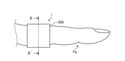
- FIG. 1A is a schematic diagram showing an example of the external appearance of a detection device according to a first embodiment when a finger is placed inside the detection device as viewed from the side of a housing.
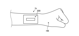
- FIG. 1B is a schematic diagram showing an example of the external appearance of the detection device according to the first embodiment when a human body is placed inside the detection device, as viewed from the side of the housing.
- FIG. 1C is a schematic diagram showing an example of the external appearance of the detection device according to the first embodiment when worn on a human body, as viewed from the side of the housing.
- FIG. 2 is a schematic cross-sectional view taken along line II-II' of FIG. 1A.
- FIG. 3 is a plan view illustrating the detection device according to the first embodiment.
- FIG. 4 is a block diagram illustrating an example of the configuration of the detection device according to the first embodiment.
- FIG. 5 is a circuit diagram showing the detection device according to the first embodiment.
- FIG. 6 is a plan view illustrating a schematic view of a plurality of pixels and a first opening portion.
- FIG. 7 is a cross-sectional view taken along line VII-VII' of FIG.
- FIG. 8 is an enlarged schematic diagram of the sensor unit.
- FIG. 9 is a cross-sectional view taken along line IX-IX' of FIG.
- FIG. 10 is a cross-sectional view taken along line XX' of FIG.
- FIG. 11 is a schematic cross-sectional view of a detection device according to a first modified example of the first embodiment.
- FIG. 12 is a schematic cross-sectional view of a detection device according to a second modification of the first embodiment.
- FIG. 13 is a schematic cross-sectional view of a detection device according to a third modification of the first embodiment.
- FIG. 14 is a plan view illustrating a plurality of pixels and a first opening of the detection device according to the second embodiment.
- FIG. 15 is an enlarged schematic configuration diagram of a sensor unit according to the second embodiment.
- FIG. 16 is a plan view illustrating a plurality of pixels and a first opening of the detection device according to the third embodiment.
- FIG. 17 is an enlarged schematic plan view of the periphery of the first opening in FIG. 16.
- FIG. 18 is a cross-sectional view taken along line XVIII-XVIII' of FIG.
- FIG. 19 is a schematic cross-sectional view of a detection device according to a first modified example of the third embodiment.
- FIG. 20 is a schematic cross-sectional view of a detection device according to a second modification of the third embodiment.
- FIG. 21 is a schematic cross-sectional view of a detection device according to a third modification of the third embodiment.
- FIG. 22 is a plan view illustrating a plurality of pixels, a first opening, and a second opening of a detection device according to a fourth embodiment.
- FIG. 23 is a cross-sectional view taken along line XXIII-XXIII' of FIG.
- FIG. 24 is an explanatory diagram for explaining the manufacturing method of the fifth embodiment.
- the term "on top” is used, unless otherwise specified, to include both a case in which another structure is placed directly on top of a structure so as to be in contact with the structure, and a case in which another structure is placed above a structure via yet another structure.
- FIG. 1A is a schematic diagram showing an example of the appearance of a detection device according to embodiment 1 when a finger is placed inside the detection device as viewed from the side of a housing.
- Fig. 2 is a schematic cross-sectional view taken along line II-II' shown in Fig. 1A.
- the detection device 1 shown in FIG. 1A is a ring-shaped device that can be attached and detached to the human body, and is worn on a finger Fg of the human body.
- the finger Fg includes the thumb, index finger, middle finger, ring finger, little finger, etc.
- the human body is the person to be authenticated, whose identity is verified by the detection device 1.
- the detection device 1 can detect biometric information about a living body from the finger Fg on which it is worn.
- the finger Fg is an example of a measurement target.
- the measurement target is a living body or a part of a living body, and is the measurement target.
- the detection device 1 is made into a ring or wristband, making it easy for the user to carry. In the following description, it is assumed that the detection device 1 is used as a ring.
- the detection device 1 includes a housing 200, light sources 53 and 54, and an organic photodiode PD (organic light sensor).
- the detection device 1 includes a battery (not shown) inside the housing 200, and is a device that operates on battery power.
- Components other than the housing 200, the organic photodiode PD, and the light sources 53 and 54 are omitted from FIG. 2.
- the housing 200 is formed in a ring shape (annular shape) that can be attached to the finger Fg, and is a wearing member that is attached to the living body.
- the housing 200 includes a sealing film 210 and an exterior part 220.
- the housing 200 is formed in a ring shape by integrating the sealing film 210 and the exterior part 220.
- the sealing film 210 houses the light sources 53, 54, the organic photodiode PD, etc. inside.
- the sealing film 210 is formed in a ring shape from a housing material such as a transparent synthetic resin or silicon.
- the exterior part 220 has a surface of the housing 200 that covers the sealing film 210.
- the exterior part 220 is formed in a ring shape from a material such as a metal or a non-transparent synthetic resin.
- the exterior part 220 has an air vent 221.
- FIG. 1B is a schematic diagram showing an example of the appearance of a human body placed inside detection device 1a according to embodiment 1, as viewed from the side of the housing.
- Detection device 1a shown in FIG. 1B is a ring-shaped device that can be attached and detached to human body HB, and is worn on the arm of human body HB.
- Detection device 1 shown in FIG. 1B is, for example, a smart watch, a wristwatch, a wristband, etc.
- Human body HB is the body of the person to be authenticated, whose identity is verified by detection device 1, and includes wrists, arms, legs, etc.
- Detection device 1 can detect biometric information related to the living body from the attached human body HB.
- FIG. 1C is a schematic diagram showing an example of the appearance of detection device 1b according to embodiment 1 when worn on a human body, as viewed from the side of the housing.
- Detection device 1b shown in FIG. 1C is a bandage-type device that can be attached and detached to human body HB, and can be attached to the surface of human body HB by being attached to the surface of human body HB or placed on the surface of human body HB.
- Detection device 1 can detect biometric information related to a living organism from the attached human body HB.
- each of the multiple first openings OP is provided penetrating the sealing film 210, the organic photodiode PD, and the first substrate 21 (see FIG. 3) in the normal direction.
- the ventilation opening 221 is provided penetrating in the normal direction in order to discharge sweat generated from the finger Fg to the outside.
- the sweat is discharged to the outside from the ventilation opening 221 via one of the multiple first openings OP.
- the multiple organic photodiodes PD detect biometric information related to the living body from a detection object such as a finger Fg. Specifically, the light emitted from the light sources 53 and 54 and transmitted through or reflected by a detection object such as a finger Fg is irradiated onto the multiple organic photodiodes PD.
- the multiple organic photodiodes PD detect light emitted by the light sources 53 and 54 and reflected by the finger Fg, etc., as well as light that is directly incident.
- the light sources 53, 54 are provided inside the sealing film 210 of the housing 200 at positions that do not overlap with the multiple organic photodiodes PD, and are configured to be able to irradiate light toward a detected object such as a finger Fg attached to the ring-shaped housing 200.
- a detected object such as a finger Fg attached to the ring-shaped housing 200.
- the positions of the light sources 53, 54 shown in FIG. 2 are merely examples and can be changed as appropriate.
- the light sources 53, 54 may be positioned in any way as long as the light emitted from the light sources 53, 54 and transmitted through or reflected by a detected object such as a finger Fg is appropriately irradiated onto the organic photodiode PD.
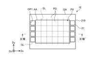
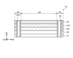
- FIG. 3 is a plan view showing a schematic diagram of the detection device according to the first embodiment.
- the detection device 1 has a first substrate 21, a sensor unit 10, a gate line driving circuit 15, a signal line selection circuit 16, a detection circuit 48, a control circuit 122, a power supply circuit 123, a first light source substrate 51, a second light source substrate 52, and light sources 53 and 54.
- a plurality of light sources 53 are provided on the first light source substrate 51.
- a plurality of light sources 54 are provided on the second light source substrate 52.
- the control board 121 is electrically connected to the first board 21 via the wiring board 71.
- the wiring board 71 is, for example, a flexible printed circuit board or a rigid board.
- the detection circuit 48 is provided on the wiring board 71.
- the control board 121 is provided with a control circuit 122 and a power supply circuit 123.
- the control circuit 122 is, for example, an FPGA (Field Programmable Gate Array).
- the control circuit 122 supplies control signals to the sensor unit 10, the gate line driving circuit 15, and the signal line selection circuit 16 to control the detection operation of the sensor unit 10.
- the control circuit 122 also supplies control signals to the light sources 53 and 54 to control the lighting or non-lighting of the light sources 53 and 54.
- the power supply circuit 123 supplies voltage signals such as a sensor power supply signal VDDSNS (see FIG. 5) to the sensor unit 10, the gate line driving circuit 15, and the signal line selection circuit 16. In addition, the power supply circuit 123 supplies power supply voltage to the light sources 53 and 54.
- VDDSNS sensor power supply signal
- the first substrate 21 has a detection area AA and a peripheral area GA.
- the detection area AA is an area in which multiple organic photodiodes PD (see FIG. 9) of the sensor unit 10 are arranged.
- the peripheral area GA is an area between the outer periphery of the detection area AA and the outer edge of the first substrate 21, and is an area in which multiple organic photodiodes PD are not provided.
- the gate line driving circuit 15 and the signal line selection circuit 16 are provided in the peripheral area GA. Specifically, the gate line driving circuit 15 is provided in a region of the peripheral area GA that extends along the second direction Dy. The signal line selection circuit 16 is provided in a region of the peripheral area GA that extends along the first direction Dx, and is provided between the sensor unit 10 and the detection circuit 48.
- the first direction Dx is a direction in a plane parallel to the first substrate 21.
- the second direction Dy is a direction in a plane parallel to the first substrate 21, and is a direction perpendicular to the first direction Dx.
- the second direction Dy may intersect the first direction Dx without being perpendicular thereto.
- the third direction Dz is a direction perpendicular to the first direction Dx and the second direction Dy, and is a normal direction to the main surface of the first substrate 21.
- plane view refers to the positional relationship when viewed from a direction perpendicular to the first substrate 21.
- the multiple light sources 53 are provided on the first light source substrate 51 and are arranged along the second direction Dy.
- the multiple light sources 54 are provided on the second light source substrate 52 and are arranged along the second direction Dy.
- the first light source substrate 51 and the second light source substrate 52 are electrically connected to the control circuit 122 and the power supply circuit 123 via terminal portions 124 and 125, respectively, provided on the control board 121.
- the multiple light sources 53, 54 may be, for example, inorganic light-emitting diodes (LEDs) or organic light-emitting diodes (OLEDs).
- the multiple light sources 53 and the multiple light sources 54 each emit light of a different predetermined wavelength.
- the light sources 53, 54 each have multiple light sources so that they can emit near-infrared light, red light, and green light.
- the first light emitted from the light source 53 is reflected by the surface of the object to be detected, such as a finger Fg, and enters the sensor unit 10. This allows the sensor unit 10 to detect a fingerprint by detecting the uneven shape of the surface of the finger Fg.
- the second light emitted from the light source 54 is reflected inside the finger Fg or passes through the finger and enters the sensor unit 10. This allows the sensor unit 10 to detect information about a living body inside the finger Fg.
- Information about a living body includes, for example, the pulse waves, pulse, and blood vessel images of the finger or palm.
- the detection device 1 may be configured as a fingerprint detection device that detects fingerprints, or a vein detection device that detects blood vessel patterns such as veins.
- the detection device 1 is provided with multiple types of light sources 53, 54 as light sources. However, this is not limited to this, and there may be only one type of light source. For example, multiple light sources 53 and multiple light sources 54 may be arranged on each of the first light source substrate 51 and the second light source substrate 52. Furthermore, there may be one or three or more light source substrates on which the light sources 53 and the light sources 54 are arranged. Alternatively, it is sufficient that at least one or more light sources are arranged.
- FIG. 4 is a block diagram showing an example of the configuration of the detection device according to the first embodiment.
- the detection device 1 further includes a detection control circuit 11 and a detection unit 40. Some or all of the functions of the detection control circuit 11 are included in the control circuit 122. In addition, some or all of the functions of the detection unit 40 other than the detection circuit 48 are included in the control circuit 122.
- the sensor unit 10 has multiple organic photodiodes PD.
- the organic photodiodes PD of the sensor unit 10 output an electrical signal corresponding to the irradiated light as a detection signal Vdet to the signal line selection circuit 16.
- the sensor unit 10 also performs detection according to the gate drive signal VGL supplied from the gate line drive circuit 15.
- the detection control circuit 11 supplies control signals to the gate line drive circuit 15, the signal line selection circuit 16, and the detection unit 40, respectively, to control their operation.
- the detection control circuit 11 supplies various control signals, such as a start signal STV and a clock signal CK, to the gate line drive circuit 15.
- the detection control circuit 11 also supplies various control signals, such as a selection signal ASW, to the signal line selection circuit 16.
- the detection control circuit 11 also supplies various control signals to the light sources 53 and 54 to control their lighting and non-lighting.
- the gate line driving circuit 15 drives multiple gate lines GL (see FIG. 5) based on various control signals.
- the gate line driving circuit 15 selects multiple gate lines GL sequentially or simultaneously, and supplies a gate driving signal VGL to the selected gate lines GL. In this way, the gate line driving circuit 15 selects multiple organic photodiodes PD connected to the gate lines GL.
- the signal line selection circuit 16 has a switch circuit that sequentially or simultaneously selects multiple signal lines SL (see FIG. 5).
- the signal line selection circuit 16 is, for example, a multiplexer.
- the signal line selection circuit 16 connects the selected signal line SL to the detection circuit 48 based on the selection signal ASW supplied from the detection control circuit 11. As a result, the signal line selection circuit 16 outputs the detection signal Vdet of the organic photodiode PD to the detection unit 40.
- the detection unit 40 includes a detection circuit 48, a signal processing circuit 44, a coordinate extraction circuit 45, a memory circuit 46, and a detection timing control circuit 47.
- the detection timing control circuit 47 controls the detection circuit 48, the signal processing circuit 44, and the coordinate extraction circuit 45 to operate in synchronization based on a control signal supplied from the detection control circuit 11.
- the detection circuit 48 is, for example, an analog front-end circuit (AFE).
- the detection circuit 48 is a signal processing circuit having at least the functions of a detection signal amplifier circuit 42 and an A/D conversion circuit 43.
- the detection signal amplifier circuit 42 amplifies the detection signal Vdet.
- the A/D conversion circuit 43 converts the analog signal output from the detection signal amplifier circuit 42 into a digital signal.
- the signal processing circuit 44 detects a predetermined physical quantity input to the sensor unit 10 based on the output signal of the detection circuit 48.
- the signal processing circuit 44 is a logic circuit. When a finger touches or approaches the detection surface, the signal processing circuit 44 can detect unevenness on the surface of the finger or palm based on the signal from the detection circuit 48.
- the signal processing circuit 44 can also detect information about the living body based on the signal from the detection circuit 48.
- the information about the living body is, for example, an image of the blood vessels in the finger or palm, pulse waves, pulse rate, blood oxygen concentration, etc.
- the memory circuit 46 temporarily stores the signal calculated by the signal processing circuit 44.
- the memory circuit 46 may be, for example, a RAM (Random Access Memory), a register circuit, etc.
- the coordinate extraction circuit 45 determines the detection coordinates of the unevenness of the surface of the finger, etc., when the signal processing circuit 44 detects contact or proximity of a finger.
- the coordinate extraction circuit 45 also determines the detection coordinates of the blood vessels in the finger or palm.
- the coordinate extraction circuit 45 is a logic circuit.
- the coordinate extraction circuit 45 combines the detection signals Vdet output from each organic photodiode PD of the sensor unit 10 to generate two-dimensional information indicating the shape of the unevenness of the surface of the finger, etc., and two-dimensional information indicating the shape of the blood vessels in the finger or palm.
- the coordinate extraction circuit 45 may output the detection signal Vdet as the sensor output voltage Vo without calculating the detection coordinates.
- FIG. 5 is a circuit diagram showing the detection device according to the first embodiment. Note that FIG. 5 also shows the circuit configuration of the detection circuit 48.
- the sensor pixel PX includes an organic photodiode PD, a capacitance element Ca, and a drive transistor Tr.
- the capacitance element Ca is a capacitance (sensor capacitance) formed in the organic photodiode PD, and is equivalently connected in parallel with the organic photodiode PD.
- FIG. 5 of the multiple gate lines GL, two gate lines GL(m) and GL(m+1) aligned in the second direction Dy are shown. Also, of the multiple signal lines SL, two signal lines SL(n) and SL(n+1) aligned in the first direction Dx are shown.
- the sensor pixel PX is the area surrounded by the gate line GL and the signal line SL.
- the drive transistor Tr is provided corresponding to each of the multiple organic photodiodes PD.
- the drive transistor Tr is composed of a thin film transistor, and in this example, is composed of an n-channel MOS (Metal Oxide Semiconductor) type TFT (Thin Film Transistor).
- Each of the multiple gate lines GL is connected to the gates of multiple drive transistors Tr arranged in a first direction Dx.
- Each of the multiple signal lines SL is connected to one of the sources and drains of multiple drive transistors Tr arranged in a second direction Dy.
- the other of the sources and drains of the multiple drive transistors Tr is connected to the anode of the organic photodiode PD and the capacitance element Ca.
- the cathode of the organic photodiode PD is supplied with a sensor power supply signal VDDSNS from the power supply circuit 123 (see FIG. 3).
- the signal line SL and the capacitance element Ca are supplied with a sensor reference voltage COM, which is the initial potential of the signal line SL and the capacitance element Ca, from the power supply circuit 123 via the reset transistor TrR.
- the switch SSW of the detection circuit 48 is turned on and connected to the signal line SL.
- the detection signal amplifier circuit 42 of the detection circuit 48 converts the current or charge supplied from the signal line SL into a voltage corresponding to the current or charge.
- a reference potential (Vref) having a fixed potential is input to the non-inverting input section (+) of the detection signal amplifier circuit 42, and the signal line SL is connected to the inverting input section (-).
- a signal equal to the sensor reference voltage COM is input as the reference potential (Vref) voltage.
- the control circuit 122 see FIG.
- the detection signal amplifier circuit 42 also has a capacitance element Cb and a reset switch RSW. During the reset period, the reset switch RSW is turned on and the charge of the capacitance element Cb is reset.
- the driving transistor Tr is not limited to an n-type TFT, and may be a p-type TFT.
- the pixel circuit of the sensor pixel PX shown in FIG. 3 is merely an example, and the sensor pixel PX may be provided with multiple transistors corresponding to one organic photodiode PD.
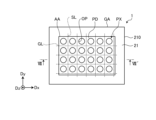
- FIG. 6 is a plan view showing a schematic diagram of a plurality of pixels and a first opening.
- each of the plurality of sensor pixels PX is arranged in a matrix in the detection area AA of the first substrate 21, and each has an organic photodiode PD.
- the sensor pixels PX are arranged in four rows and six columns.
- FIG. 6 shows a simplified arrangement of the sensor pixels PX for ease of understanding.
- the detection device 1 may have a large number of sensor pixels PX in five rows and seven columns or more, depending on the type of object to be detected and the detection resolution.
- the multiple gate lines GL each extend in a first direction Dx and are arranged at intervals in the second direction Dy.
- the multiple signal lines SL each extend in the second direction Dy and are arranged at intervals in the first direction Dx.
- the multiple sensor pixels PX multiple organic photodiodes PD are provided in an area surrounded by adjacent gate lines GL and adjacent signal lines SL.
- the sealing film 210 is provided to cover a detection area AA having a plurality of sensor pixels PX (a plurality of organic photodiodes PD).
- the detection device 1 has a plurality of first openings OP in the detection area AA.
- the plurality of first openings OP are provided in areas overlapping with each of the sensor pixels PX, and are arranged in a matrix in the detection area AA. In other words, each of the plurality of first openings OP is provided in an area surrounded by two gate lines GL and two signal lines SL.
- the multiple first openings OP are circular in plan view.
- the areas (diameters) of the multiple first openings OP are substantially equal to each other.
- the areas (diameters) of the first openings OP are all equal to each other, but some of them may be different.
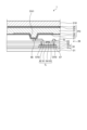
- FIG. 7 is a cross-sectional view taken along line VII-VII' in FIG. 6. Note that in FIG. 7, the configuration of each layer is shown in a simplified manner for ease of understanding. The detailed layered configuration of the organic photodiode PD will be described later in FIG. 9. Also, the detailed layered configuration of the circuit formation layer 29 will be described later in FIG. 10.
- the direction perpendicular to the surface of the first substrate 21, from the first substrate 21 toward the sealing film 210 is referred to as the "upper side” or simply “upper”.
- the direction from the sealing film 210 toward the first substrate 21 is referred to as the "lower side” or simply “lower”.
- the detection device 1 is formed by stacking a circuit formation layer 29, an organic photodiode PD, and a sealing film 210 in this order on a first substrate 21.
- the circuit formation layer 29 is provided on the first substrate 21, and is a layer on which various transistors such as the drive transistor Tr shown in FIG. 5, and various wiring such as the gate line GL and the signal line SL are formed.
- the organic photodiode PD is provided on the circuit formation layer 29.
- the organic photodiode PD is provided continuously across the detection area AA and the peripheral area GA. Note that the organic photodiode PD provided in the peripheral area GA is configured not to function as an optical sensor.
- the sealing film 210 is provided on the organic photodiode PD.
- a plurality of first openings OP are provided penetrating from the sealing film 210 to the first substrate 21 in the third direction Dz.
- the plurality of first openings OP are provided in an area overlapping with the detection area AA, and are not provided in an area overlapping with the peripheral area GA.
- the side walls of the multiple first openings OP are covered with a resin film 55.
- the resin film 55 is formed, for example, from a film-like synthetic resin such as PET (Poly Ethylene Terephthalate).
- PET Poly Ethylene Terephthalate
- the resin film 55 has a shape that matches the shape of the side walls of the first openings OP, and the shape is not particularly limited, and may be curved or rectangular. This allows the organic photodiode PD, the circuit formation layer 29, and the first substrate 21 to be sealed.
- Figure 8 is an enlarged schematic diagram of the sensor section. Note that in Figure 8, multiple first openings OP are indicated by two-dot chain lines to make the drawing easier to see.
- the detection device 1 has a plurality of organic photodiodes PD provided on a first substrate 21.
- the right and bottom edges of the lower electrode 23 are provided so as to overlap with a portion of the signal line SL and the gate line GL, respectively.
- the left and top edges of the lower electrode 23 are provided so as not to overlap with the signal line SL and the gate line GL, respectively.
- the first openings OP are provided in areas where the lower electrodes 23 are not arranged in a plan view. This prevents the lower electrodes 23 from being exposed to the first openings OP, ensuring reliability.
- the driving transistor Tr has a semiconductor layer 61, a source electrode 62, a drain electrode 63, and a gate electrode 64.
- the semiconductor layer 61 extends along the gate line GL and is disposed so as to intersect with the gate electrode 64 in a planar view.
- the gate electrode 64 is connected to the gate line GL and extends in a direction (second direction Dy) perpendicular to the gate line GL.
- One end of the semiconductor layer 61 is connected to a source electrode 62 via contact hole CH2.
- the source electrode 62 is connected to a connection pad 66 and is drawn out to the center of the lower electrode 23.
- the lower electrode 23 is connected to the connection pad 66 at its center via contact hole CH1.
- the source electrode 62 of the drive transistor Tr is electrically connected to the organic photodiode PD.
- the other end of the semiconductor layer 61 is connected to a drain electrode 63 via contact hole CH3.
- the drain electrode 63 is connected to a signal line SL.
- the shape, arrangement pitch, etc. of the lower electrodes 23 shown in FIG. 8 are merely examples and can be changed as appropriate depending on the characteristics and detection accuracy required for the detection device 1.
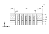
- FIG. 9 is a cross-sectional view taken along line IX-IX' in FIG. 8.
- FIG. 10 is a cross-sectional view taken along line X-X' in FIG. 8.
- the detection device 1 has a circuit formation layer 29, an insulating film 27, an organic photodiode PD, and a sealing film 210 laminated in this order on a first substrate 21.
- the first substrate 21 is an insulating substrate, and may be, for example, a glass substrate such as quartz or non-alkali glass.
- the first substrate 21 is not limited to being flat, and may have a curved surface. In this case, the first substrate 21 is formed in a strip shape from, for example, a film-like synthetic resin such as PET (Poly Ethylene Terephthalate).
- the circuit formation layer 29 is provided on the first substrate 21.
- the insulating film 27 is provided on the circuit formation layer 29 including the drive transistor Tr, covering the signal line SL.
- the insulating film 27 is an organic planarization film made of an organic insulating material.
- the circuit formation layer 29 has an undercoat film 91, a gate insulating film 92, and an interlayer insulating film 93 as insulating films.
- the undercoat film 91 has, for example, a two-layer laminated structure having insulating films 91a and 91b.
- the undercoat film 91 is formed of, for example, an inorganic insulating film such as a silicon nitride film or a silicon oxide film. Note that the configuration of the undercoat film 91 is not limited to that shown in FIG. 12.
- the undercoat film 91 may be a single layer film or a laminate of three or more layers.
- the light-shielding film 67 is provided on the insulating film 91a.
- the light-shielding film 67 is provided between the semiconductor layer 61 and the first substrate 21.
- the light-shielding film 67 can suppress the intrusion of light from the first substrate 21 side into the channel region of the semiconductor layer 61.
- the drive transistor Tr is provided on the first substrate 21.
- the semiconductor layer 61 is provided on the undercoat film 91.
- the gate insulating film 92 is provided on the undercoat film 91, covering the semiconductor layer 61.
- the gate insulating film 92 is an inorganic insulating film, such as a silicon oxide film.
- the gate electrode 64 is provided on the gate insulating film 92.
- the driving transistor Tr has a top gate structure.
- the driving transistor Tr is not limited to this, and may have a bottom gate structure or a dual gate structure in which a gate electrode 64 is provided on both the upper and lower sides of the semiconductor layer 61.
- the interlayer insulating film 93 is provided on the gate insulating film 92, covering the gate electrode 64.
- the interlayer insulating film 93 has, for example, a laminated structure of a silicon nitride film and a silicon oxide film.
- the source electrode 62 and the drain electrode 63 are provided on the interlayer insulating film 93.
- the source electrode 62 is connected to the source region of the semiconductor layer 61 through a contact hole CH2 provided in the gate insulating film 92 and the interlayer insulating film 93.
- the drain electrode 63 is connected to the drain region of the semiconductor layer 61 through a contact hole CH3 provided in the gate insulating film 92 and the interlayer insulating film 93.
- the contact hole CH1 is provided in the lower electrode 23, penetrating the insulating film 27 in the thickness direction (third direction Dz).
- the lower electrode 23 is connected to the connection pad 66 at the bottom of the contact hole CH1.
- the insulating film 27 is provided on the interlayer insulating film 93, covering the source electrode 62 and drain electrode 63 of the drive transistor Tr.
- the contact hole CH1 of the insulating film 27 is provided in a region overlapping with the source electrode 62.
- the organic photodiode PD is provided on the insulating film 27.
- the organic photodiode PD has a lower electrode 23, a lower buffer layer 32, an active layer 31, an upper buffer layer 33, and an upper electrode 24.
- the organic photodiode PD is stacked in the following order: lower electrode 23, lower buffer layer 32, active layer 31, upper buffer layer 33, and upper electrode 24.
- the organic photodiode PD of this embodiment is an OPD (Organic Photodiode) in which an organic semiconductor is used as the active layer 31.
- the lower electrode 23 is an anode electrode of the organic photodiode PD, and is formed of a conductive material having light transmission, such as ITO (Indium Tin Oxide).
- the lower electrode 23 is provided separately for each organic photodiode PD.
- the lower buffer layer 32, the active layer 31, the upper buffer layer 33, and the upper electrode 24 are provided continuously across a plurality of organic photodiodes PD. Specifically, the lower buffer layer 32, the active layer 31, the upper buffer layer 33, and the upper electrode 24 are provided overlapping the lower electrode 23 of the adjacent organic photodiode PD and the lower electrode 23 of the organic photodiode PD.
- the lower electrode 23 is electrically connected to the source electrode 62 at the bottom of the contact hole CH1 near the drive transistor Tr.
- the lower buffer layer 32, the active layer 31, the upper buffer layer 33, and the upper electrode 24 may be separated for each sensor pixel PX.
- the characteristics (for example, voltage-current characteristics and resistance value) of the active layer 31 change depending on the light irradiated.
- An organic material is used as the material of the active layer 31.
- the active layer 31 is a bulk heterostructure in which a p-type organic semiconductor and an n-type fullerene derivative (PCBM), which is an n-type organic semiconductor, are mixed.
- PCBM n-type fullerene derivative
- low molecular weight organic materials such as C60 (fullerene), PCBM (phenyl C61-butyric acid methyl ester), CuPc (copper phthalocyanine), F16CuPc (fluorinated copper phthalocyanine), rubrene (5,6,11,12-tetraphenyltetracene), and PDI (perylene derivative) can be used as the active layer 31.
- C60 fulllerene
- PCBM phenyl C61-butyric acid methyl ester
- CuPc copper phthalocyanine
- F16CuPc fluorinated copper phthalocyanine
- rubrene 5,6,11,12-tetraphenyltetracene
- PDI perylene derivative
- the active layer 31 can be formed by a deposition type (dry process) using these low molecular weight organic materials.
- the active layer 31 may be, for example, a laminated film of CuPc and F16CuPc, or a laminated film of rubrene and C60.
- the active layer 31 can also be formed by a coating type (wet process).
- the active layer 31 is made of a material that combines the above-mentioned low molecular weight organic material and a polymer organic material.
- the polymer organic material for example, P3HT (poly(3-hexylthiophene)), F8BT (F8-alt-benzothiadiazole), etc. can be used.
- the active layer 31 can be a film in which P3HT and PCBM are mixed, or a film in which F8BT and PDI are mixed.
- the lower buffer layer 32 is a hole transport layer
- the upper buffer layer 33 is an electron transport layer.
- the lower buffer layer 32 and the upper buffer layer 33 are provided to facilitate the arrival of holes and electrons generated in the active layer 31 at the lower electrode 23 or the upper electrode 24.
- the lower buffer layer 32 (hole transport layer) is in direct contact with the upper surface of the lower electrode 23, and is also provided on the insulating film 35 between adjacent lower electrodes 23.
- the active layer 31 is in direct contact with the upper surface of the lower buffer layer 32.
- the material of the hole transport layer is a metal oxide layer. As the metal oxide layer, tungsten oxide (WO 3 ), molybdenum oxide, or the like is used.
- the upper buffer layer 33 (electron transport layer) is in direct contact with the active layer 31, and the upper electrode 24 is in direct contact with the upper buffer layer 33.
- the material used for the electron transport layer is ethoxylated polyethyleneimine (PEIE).
- the materials and manufacturing methods of the lower buffer layer 32, active layer 31, and upper buffer layer 33 are merely examples, and other materials and manufacturing methods may be used.
- the lower buffer layer 32 and upper buffer layer 33 are not limited to single-layer films, and may be formed as laminated films including an electron blocking layer and a hole blocking layer.
- the lower buffer layer 32 may be an electron transport layer
- the upper buffer layer 33 may be a hole transport layer
- the lower electrode 23 may be a cathode electrode
- the upper electrode 24 may be an anode electrode.
- the upper electrode 24 is provided on the upper buffer layer 33.
- the upper electrode 24 is a cathode electrode of the organic photodiode PD, and is formed continuously over the entire detection area AA. In other words, the upper electrode 24 is provided continuously over the multiple organic photodiodes PD.
- the upper electrode 24 faces the multiple lower electrodes 23, sandwiching the lower buffer layer 32, the active layer 31, and the upper buffer layer 33.
- the upper electrode 24 is formed of a conductive material having translucency, such as ITO or IZO.
- the upper electrode 24 may be a laminated film of multiple conductive materials having translucency. Note that when the upper electrode 24 is not present, the upper buffer layer 33 also functions as the upper electrode 24, and becomes the cathode electrode of the photodiode PD.
- the sealing film 210 is provided to cover the multiple organic photodiodes PD. Specifically, the sealing film 210 is provided on the upper electrode 24. Note that if the sealing film 210 is not present, the upper electrode 24 also functions as the sealing film 210.
- each of the first openings OP is provided penetrating the sealing film 210, the organic photodiode PD (the lower buffer layer 32, the active layer 31, the upper buffer layer 33, and the upper electrode 24) excluding the lower electrode 23, the insulating film 27, the circuit formation layer 29, and the first substrate 21 in the third direction Dz.
- the portion where the first openings OP are not provided overlaps at least the signal line SL and the gate line GL (see FIG. 8).
- a plurality of first openings OP are provided in an area that overlaps with the detection area AA and comes into contact with the finger Fg, etc.
- the shape, position, number, etc. of the first openings OP shown in Figures 6 to 10 are merely examples and can be changed as appropriate depending on the arrangement of the organic photodiode PD, etc.
- the configuration of the organic photodiode PD shown in Figures 9 and 10 is merely an example and can be changed as appropriate.
- the upper electrode 24 may be the anode electrode of the organic photodiode PD
- the lower electrode 23 may be the cathode electrode of the organic photodiode PD.
- (First Modification of First Embodiment) 11 is a schematic cross-sectional view of a detection device according to Modification 1 of the first embodiment.
- the same components as those described in the above embodiment are denoted by the same reference numerals, and duplicated description will be omitted.
- the sidewall of the first opening OP is covered with the same material 211 as the sealing film 210, as compared to the detection device 1 according to the first embodiment.
- the sidewall of the first opening OP can be easily covered with only the sealing film 210, without using a member such as the resin film 55.
- Modification 2 of the First Embodiment 12 is a schematic cross-sectional view of a detection device according to Modification 2 of the first embodiment.
- the same components as those described in the above embodiment are denoted by the same reference numerals, and duplicated description will be omitted.
- a second substrate 50 is provided on the sealing film 210, as compared to the detection device 1 according to the first embodiment.
- a plurality of first openings OP are provided penetrating from the second substrate 50 to the first substrate 21 in the third direction Dz.
- the sidewalls of the first openings OP provided in the second substrate 50 are covered with a resin film 55.
- the second substrate 50 overlaps with the first substrate 21 in the third direction Dz and faces the first substrate 21.
- the second substrate 50 is an insulating substrate, similar to the first substrate 21, and may be, for example, a glass substrate such as quartz or alkali-free glass.
- the second substrate 50 is not limited to a flat plate shape, and may have a curved surface.
- the second substrate 50 is formed in a band shape from, for example, PET (Poly Ethylene Terephthalate), which is a film-like synthetic resin.
- PET Poly Ethylene Terephthalate
- the second substrate 50 covers the sealing film 210, and is a deformable substrate.
- the configuration and operation of the detection device 1B related to the detection device 2 according to the first embodiment are substantially the same as those of the detection device 1 according to the first embodiment, and therefore will not be described here.
- (Variation 3 of the First Embodiment) 13 is a schematic cross-sectional view of a detection device according to Modification 3 of the first embodiment.
- the same components as those described in the above embodiment are denoted by the same reference numerals, and duplicated description will be omitted.
- a second substrate 50 is provided on the sealing film 210, as compared to the detection device 1 according to the first embodiment.
- a first opening OP is provided penetrating from the second substrate 50 to the first substrate 21 in the third direction Dz.
- the sidewall of the first opening OP is covered not with a resin film 55 but with the same material 56 as the second substrate 50.
- Fig. 14 is a plan view showing a plurality of pixels and a first opening of a detection device according to the second embodiment.
- Fig. 15 is an enlarged schematic diagram of a sensor unit according to the second embodiment.
- the same components as those described in the above-mentioned embodiment are given the same reference numerals, and duplicated description is omitted.
- the same components as those described in the first embodiment are given the same reference numerals.
- each of the first openings OP is provided in a substantially rectangular shape in a region surrounded by the gate lines GL and the signal lines SL. More specifically, as shown in FIG. 15, the first openings OP extend along the gate lines GL and the signal lines SL. Furthermore, the first openings OP are provided in regions that do not overlap with the electrodes of the drive transistors Tr.
- the area of the first opening OP is larger in the detection area AA compared to the detection device 1 according to the first embodiment, so that stuffiness caused by sweat can be more effectively suppressed.
- Fig. 16 is a plan view showing a plurality of pixels and a first opening of a detection device according to a third embodiment.
- Fig. 17 is a plan view showing an enlarged schematic view of a photosensor in the peripheral region of Fig. 16.
- Fig. 18 is a cross-sectional view taken along line XVIII-XVIII' of Fig. 16.
- the same components as those described in the above-mentioned embodiments are designated by the same reference numerals, and duplicated description will be omitted.
- a plurality of organic photodiodes PD are provided in the detection area AA and the peripheral area GA of the first substrate 21.
- a plurality of first openings OP1 are provided in the peripheral area GA in the second direction Dy, in an area surrounded by the gate lines GL and the signal lines SL.
- the pitch of the multiple gate lines GL1 aligned adjacent to the first opening OP1 in the peripheral area GA is narrower than the pitch of the gate lines GL in the detection area AA.
- the pitch of the multiple signal lines SL aligned adjacent to the first opening OP1 may be narrower than the pitch of the signal lines SL in the detection area AA.
- the distance L2 between the multiple gate lines GL1 in the peripheral area GA is narrower than the distance L1 between the multiple gate lines GL in the detection area AA, making it easier to form the first opening OP1.
- the first openings OP1 are provided penetrating from the sealing film 210 to the first substrate 21 in the third direction Dz.
- the multiple first openings OP1 are provided in an area overlapping with the peripheral area GA, and are not provided in an area overlapping with the detection area AA.
- the side walls of the multiple first openings OP1 are covered with a resin film 55.
- first openings OP1 are merely examples and can be changed as appropriate.
- the first openings OP1 are not provided in some areas of the peripheral area GA, but are not limited to this and may be provided, for example, in the entire peripheral area GA.
- the detection device 1E according to the third embodiment can be combined with the detection device 1 according to the first embodiment. That is, a configuration in which a plurality of first openings OP, OP1 are provided in the detection area AA and the surrounding area GA can be adopted. In this case, it is possible to more effectively suppress stuffiness due to sweat.
- (Variation 1 of the third embodiment) 19 is a schematic cross-sectional view of a detection device according to Modification 1 of the third embodiment.
- the same components as those described in the above embodiment are denoted by the same reference numerals, and duplicated description will be omitted.
- the sidewall of the first opening OP1 is covered with the same material 211 as the sealing film 210.
- the sidewall of the first opening OP1 can be easily covered with only the sealing film 210, without using a member such as the resin film 55.
- Modification 2 of embodiment 3 20 is a schematic cross-sectional view of a detection device according to Modification 2 of the third embodiment.
- the same components as those described in the above embodiment are denoted by the same reference numerals, and duplicated description will be omitted.
- a second substrate 50 is provided on a sealing film 210.
- a first opening OP1 is provided penetrating from the second substrate 50 to the first substrate 21 in the third direction Dz.
- the sidewall of the first opening OP provided in the second substrate 50 is covered with a resin film 55.
- the configuration and operation of the detection device 1G according to the second modified example of the third embodiment are substantially the same as those of the detection device 1E according to the third embodiment, and therefore will not be described.
- (Variation 3 of embodiment 3) 21 is a schematic cross-sectional view of a detection device according to Modification 3 of the third embodiment.
- the same components as those described in the above embodiment are denoted by the same reference numerals, and duplicated description will be omitted.
- a second substrate 50 is provided on a sealing film 210.
- a first opening OP is provided penetrating from the second substrate 50 to the first substrate 21 in the third direction Dz.
- the sidewall of the first opening OP1 is covered not with a resin film 55 but with the same material 56 as the second substrate 50.
- Fig. 22 is a plan view showing a plurality of pixels, a first opening, and a second opening of a detection device according to a fourth embodiment.
- Fig. 23 is a cross-sectional view taken along line XXI-XXI' of Fig. 22.
- the same components as those described in the above-mentioned embodiments are designated by the same reference numerals, and duplicated description will be omitted.
- a second substrate 50 is provided on the sealing film 210.
- the second substrate 50 has a plurality of second openings OP2.
- the second substrate 50 is made of a mesh-shaped material in a plan view. Furthermore, each of the second openings OP2 overlaps, in whole or in part, with the first opening OP.
- Each of the plurality of second openings OP2 is on the order of microns in size.
- the second substrate 50 has a single-layer structure.
- the second substrate 50 is not limited to this, and may be, for example, a laminate of two or more layers.
- center-to-center distances D1 to D14 of the multiple second openings OP2 are different, but the center-to-center distances X1 to X5 of the multiple first openings OP are the same.
- the manufacturing method of the fifth embodiment is a manufacturing method for manufacturing a detection device 1C according to the third modification of the first embodiment.
- FIG. 24 is an explanatory diagram for explaining the manufacturing method of the fifth embodiment.
- the configuration of each layer is simplified for ease of understanding.
- the same components as those described in the above-mentioned embodiment are denoted by the same reference numerals, and duplicated description will be omitted.
- the circuit formation layer 29, the organic photodiode PD, and the sealing film 210 are stacked in this order on the first substrate 21 (step ST1).
- a first opening OP is formed penetrating from the sealing film 210 to the first substrate 21 in the third direction Dz (step ST2).
- the second substrate 50 is laminated on the sealing film 210 (step ST3).
- the second substrate 50 is heated (step ST4).
- the heating process is, for example, a reflow process.
- step ST4 the portion of the second substrate 50 that overlaps with the first opening OP melts and deforms due to the pressure difference between the second substrate 50 and the first opening OP.
- step ST4 the portion of the second substrate 50 that overlaps with the first opening OP deforms in the third direction Dz along the inner wall of the hole toward the first substrate 21 (step ST4).
- step ST4 the sidewall of the first opening OP is covered with the same material 56 as the second substrate 50, and when the heating is completed, the material 56 hardens. In this manner, a detection device 1C according to the third modification of the first embodiment is manufactured.
- a hole can be easily formed in the portion of the second substrate 50 that overlaps with the first opening OP from a single plate, and the side wall of the first opening OP can be covered. Note that the manufacturing method shown in FIG. 24 is merely an example and can be modified as appropriate.
Landscapes
- Solid State Image Pick-Up Elements (AREA)
Priority Applications (1)
| Application Number | Priority Date | Filing Date | Title |
|---|---|---|---|
| JP2025535676A JPWO2025022960A1 (https=) | 2023-07-24 | 2024-07-03 |
Applications Claiming Priority (2)
| Application Number | Priority Date | Filing Date | Title |
|---|---|---|---|
| JP2023-120200 | 2023-07-24 | ||
| JP2023120200 | 2023-07-24 |
Publications (1)
| Publication Number | Publication Date |
|---|---|
| WO2025022960A1 true WO2025022960A1 (ja) | 2025-01-30 |
Family
ID=94374955
Family Applications (1)
| Application Number | Title | Priority Date | Filing Date |
|---|---|---|---|
| PCT/JP2024/024109 Pending WO2025022960A1 (ja) | 2023-07-24 | 2024-07-03 | 検出装置及び検出装置の製造方法 |
Country Status (2)
| Country | Link |
|---|---|
| JP (1) | JPWO2025022960A1 (https=) |
| WO (1) | WO2025022960A1 (https=) |
Citations (8)
| Publication number | Priority date | Publication date | Assignee | Title |
|---|---|---|---|---|
| JP2006186032A (ja) * | 2004-12-27 | 2006-07-13 | Canon Inc | 放射線撮像装置 |
| WO2017221558A1 (ja) * | 2016-06-21 | 2017-12-28 | ソニー株式会社 | 半導体装置、及び半導体装置の製造方法 |
| JP2018149280A (ja) * | 2017-03-13 | 2018-09-27 | ヤマハ株式会社 | 生体振動センサー |
| WO2020091012A1 (ja) * | 2018-10-31 | 2020-05-07 | 大日本印刷株式会社 | 配線基板及び配線基板の製造方法 |
| WO2020262288A1 (ja) * | 2019-06-27 | 2020-12-30 | パナソニックIpマネジメント株式会社 | 伸縮性回路基板、及び伸縮性回路実装品 |
| JP2021064681A (ja) * | 2019-10-11 | 2021-04-22 | 大日本印刷株式会社 | 配線基板及び配線基板の製造方法 |
| JP2022024636A (ja) * | 2020-07-28 | 2022-02-09 | 株式会社ジャパンディスプレイ | 検出装置 |
| JP2023030472A (ja) * | 2021-08-23 | 2023-03-08 | 株式会社ジャパンディスプレイ | 検出装置 |
-
2024
- 2024-07-03 JP JP2025535676A patent/JPWO2025022960A1/ja active Pending
- 2024-07-03 WO PCT/JP2024/024109 patent/WO2025022960A1/ja active Pending
Patent Citations (8)
| Publication number | Priority date | Publication date | Assignee | Title |
|---|---|---|---|---|
| JP2006186032A (ja) * | 2004-12-27 | 2006-07-13 | Canon Inc | 放射線撮像装置 |
| WO2017221558A1 (ja) * | 2016-06-21 | 2017-12-28 | ソニー株式会社 | 半導体装置、及び半導体装置の製造方法 |
| JP2018149280A (ja) * | 2017-03-13 | 2018-09-27 | ヤマハ株式会社 | 生体振動センサー |
| WO2020091012A1 (ja) * | 2018-10-31 | 2020-05-07 | 大日本印刷株式会社 | 配線基板及び配線基板の製造方法 |
| WO2020262288A1 (ja) * | 2019-06-27 | 2020-12-30 | パナソニックIpマネジメント株式会社 | 伸縮性回路基板、及び伸縮性回路実装品 |
| JP2021064681A (ja) * | 2019-10-11 | 2021-04-22 | 大日本印刷株式会社 | 配線基板及び配線基板の製造方法 |
| JP2022024636A (ja) * | 2020-07-28 | 2022-02-09 | 株式会社ジャパンディスプレイ | 検出装置 |
| JP2023030472A (ja) * | 2021-08-23 | 2023-03-08 | 株式会社ジャパンディスプレイ | 検出装置 |
Also Published As
| Publication number | Publication date |
|---|---|
| JPWO2025022960A1 (https=) | 2025-01-30 |
Similar Documents
| Publication | Publication Date | Title |
|---|---|---|
| JP7751416B2 (ja) | 検出装置 | |
| JP7633109B2 (ja) | 検出装置 | |
| JP7818127B2 (ja) | 検出装置 | |
| JP7780628B2 (ja) | 検出装置 | |
| JP7806217B2 (ja) | 検出装置 | |
| JP7645689B2 (ja) | 検出装置及び撮像装置 | |
| JP2026020189A (ja) | 電子機器 | |
| JP7659640B2 (ja) | 検出装置 | |
| JP7606941B2 (ja) | 検出装置 | |
| WO2025022960A1 (ja) | 検出装置及び検出装置の製造方法 | |
| JP2024136770A (ja) | 検出装置 | |
| JP7770895B2 (ja) | 電子機器 | |
| US20260033723A1 (en) | Detection device | |
| US20240196634A1 (en) | Detection device and method for manufacturing same | |
| JP7823925B2 (ja) | 光学式センサ | |
| JP2025148873A (ja) | 電子機器 | |
| WO2024135561A1 (ja) | 検出装置 | |
| JP2022190538A (ja) | 検出装置 | |
| US20250255085A1 (en) | Detection device | |
| WO2024185478A1 (ja) | 検出装置 | |
| WO2024135768A1 (ja) | 検出装置 | |
| WO2024262191A1 (ja) | 検出装置及び検出装置の製造方法 | |
| WO2025105160A1 (ja) | 検出装置 | |
| WO2026048984A1 (ja) | 検出装置 | |
| WO2024257502A1 (ja) | 検出装置 |
Legal Events
| Date | Code | Title | Description |
|---|---|---|---|
| ENP | Entry into the national phase |
Ref document number: 2025535676 Country of ref document: JP Kind code of ref document: A |
|
| WWE | Wipo information: entry into national phase |
Ref document number: 2025535676 Country of ref document: JP |
|
| NENP | Non-entry into the national phase |
Ref country code: DE |