WO2025018043A1 - サーマルプリントヘッド - Google Patents
サーマルプリントヘッド Download PDFInfo
- Publication number
- WO2025018043A1 WO2025018043A1 PCT/JP2024/020147 JP2024020147W WO2025018043A1 WO 2025018043 A1 WO2025018043 A1 WO 2025018043A1 JP 2024020147 W JP2024020147 W JP 2024020147W WO 2025018043 A1 WO2025018043 A1 WO 2025018043A1
- Authority
- WO
- WIPO (PCT)
- Prior art keywords
- layer
- thermal printhead
- glaze
- main surface
- glaze layer
- Prior art date
- Legal status (The legal status is an assumption and is not a legal conclusion. Google has not performed a legal analysis and makes no representation as to the accuracy of the status listed.)
- Pending
Links
Images







Classifications
-
- B—PERFORMING OPERATIONS; TRANSPORTING
- B41—PRINTING; LINING MACHINES; TYPEWRITERS; STAMPS
- B41J—TYPEWRITERS; SELECTIVE PRINTING MECHANISMS, i.e. MECHANISMS PRINTING OTHERWISE THAN FROM A FORME; CORRECTION OF TYPOGRAPHICAL ERRORS
- B41J2/00—Typewriters or selective printing mechanisms characterised by the printing or marking process for which they are designed
- B41J2/315—Typewriters or selective printing mechanisms characterised by the printing or marking process for which they are designed characterised by selective application of heat to a heat sensitive printing or impression-transfer material
- B41J2/32—Typewriters or selective printing mechanisms characterised by the printing or marking process for which they are designed characterised by selective application of heat to a heat sensitive printing or impression-transfer material using thermal heads
- B41J2/335—Structure of thermal heads
Definitions
- This disclosure relates to a thermal printhead.
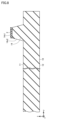
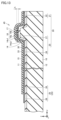
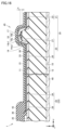
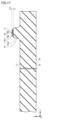
- FIG. 16 is a schematic partial enlarged cross-sectional view of a thermal printhead according to the second embodiment.
- FIG. 17 is a schematic partial enlarged sectional view showing a step subsequent to the step shown in FIG. 8 in the method of manufacturing the thermal printhead according to the second embodiment.
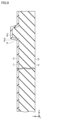
- FIG. 18 is a schematic, partially enlarged sectional view showing a step subsequent to the step shown in FIG. 17 in the method of manufacturing the thermal printhead according to the second embodiment.
- Fig. 1 is a schematic cross-sectional view of a thermal printhead 1 according to a first embodiment.
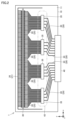
- Fig. 2 is a schematic plan view of the thermal printhead 1 according to a first embodiment.
- Fig. 3 is a schematic partial enlarged plan view of the thermal printhead 1 according to a first embodiment.
- Fig. 4 is a schematic partial enlarged cross-sectional view of the thermal printhead 1 according to a first embodiment.
- the thermal printhead 1 is an electronic device that prints on a print medium 47 such as thermal paper by selectively heating a number of heat generating elements 31 (see FIG. 3).
- the thermal printhead 1 mainly comprises a substrate 10, an insulating layer 15, a wiring layer 20, a resistor layer 30, a protective layer 33, a drive circuit 35, conductive wires 36 and 37, a connector 40, a sealing member 43, and a heat sink 49.
- the substrate 10 has a principal surface 11 and a rear surface 12 opposite the principal surface 11.
- the principal surface 11 and the rear surface 12 each extend in the x direction and the y direction perpendicular to the x direction.
- the x direction is the longitudinal direction of the substrate 10 and the main scanning direction of the thermal printhead 1.
- the y direction is the lateral direction of the substrate 10 and the sub-scanning direction of the thermal printhead 1.
- the z direction is the thickness direction of the substrate 10.
- the normal direction of the principal surface 11 is the z direction perpendicular to the x and y directions.
- the principal surface 11 faces the +z direction.
- the rear surface 12 faces the -z direction.
- the material constituting the substrate 10 is silicon.
- the substrate 10 has a protrusion 14 on the main surface 11.
- the protrusion 14 is formed by wet etching, for example, with an aqueous solution of potassium hydroxide (KOH), as described below.
- KOH potassium hydroxide
- the material constituting the substrate 10 is preferably silicon.
- the longitudinal direction of the protrusion 14 is the x-direction
- the lateral direction of the protrusion 14 is the y-direction.
- the height direction of the protrusion 14 is the z-direction.
- the protrusion 14 has a top surface 14s1 and a pair of inclined surfaces 14s2.
- the top surface 14s1 is the surface furthest from the main surface 11 in the z direction.
- the top surface 14s1 may extend in the x direction and the y direction.
- the pair of inclined surfaces 14s2 are disposed apart from each other in the y direction.
- the pair of inclined surfaces 14s2 connect the main surface 11 and the top surface 14s1.
- the pair of inclined surfaces 14s2 are inclined with respect to the main surface 11 so as to approach each other from the main surface 11 to the top surface 14s1.
- the inclination angle ⁇ of each of the pair of inclined surfaces 14s2 with respect to the main surface 11 is, for example, 54.7°.
- the substrate 10 having the protrusions 14 includes a single crystal of silicon (Si).
- the plane orientation of the main surface 11 and the back surface 12 is the (100) plane.
- the plane orientation of the pair of inclined surfaces 14s2 is the (111) plane.
- the insulating layer 15 is disposed on at least a portion of the main surface 11 and the convex portion 14, and covers at least a portion of the main surface 11 and the convex portion 14.
- the insulating layer 15 may cover the entire main surface 11.
- the material constituting the insulating layer 15 is an oxide film such as silicon dioxide (SiO 2 ).
- the oxide film such as silicon dioxide is formed by, for example, thermal oxidation.
- An oxide film (TEOS oxide film) formed using, for example, tetraethyl orthosilicate (TEOS) may be disposed on the oxide film formed by thermal oxidation.
- the TEOS oxide film is formed by stacking thin films of silicon dioxide multiple times using the plasma CVD method.
- the silicon dioxide is formed using tetraethyl orthosilicate as the raw material gas.
- the thickness of the TEOS oxide film in the z direction is, for example, 2.5 ⁇ m.
- the wiring layer 20 is connected to the resistor layer 30.
- the wiring layer 20 forms a conductive path for passing electricity to the multiple heat generating portions 31 of the resistor layer 30.
- the wiring layer 20 is electrically connected to the multiple heat generating portions 31.
- the wiring layer 20 may be, for example, a conductive material containing at least one of titanium (Ti) and copper (Cu).
- the wiring layer 20 may be aluminum (Al).
- the wiring layer 20 includes a common wiring 21, a plurality of individual wirings 25, and a plurality of lead-out wirings 29.
- the plurality of individual wirings 25 are separated from the common wiring 21 and the plurality of lead-out wirings 29.
- a current flows from the common wiring 21 toward the plurality of individual wirings 25 via the plurality of heat generating portions 31.
- the terminal portion 28 is disposed on the other side in the y direction (-y side) with respect to the resistor layer 30.
- the terminal portion 28 is disposed on the opposite side of the resistor layer 30 from the base portion 22 of the common wiring 21 in the y direction.
- the conductive wire 36 is bonded to the terminal portion 28 and the drive circuit 35.
- the terminal portion 28 is electrically connected to the drive circuit 35 through the conductive wire 36.
- the extension 26 is connected to the terminal portion 28.
- An end 27 of the extension 26 opposite the terminal portion 28 is in contact with the resistor layer 30.
- the end 27 of the extension 26 overlaps the protrusion 14.
- the resistor layer 30 includes a plurality of heat generating portions 31.
- a region of the resistor layer 30 sandwiched between a portion covered by one of the extension portions 26 of the common wiring 21 and a portion covered by one of the ends 27 of the individual wirings 25 adjacent to that portion in the x direction is one of the heat generating portions 31.
- the heat generating portions 31 are connected to the insulating layer 15.
- the heat generating portions 31 are arranged along the x direction. In a plan view of the main surface 11, the heat generating portions 31 overlap the protrusions 14. In a plan view of the main surface 11, the heat generating portions 31 are arranged inside the protrusions 14 in the short-side direction (y direction) of the resistor layer 30.
- the protective layer 33 covers the resistor layer 30, the wiring layer 20, and the multiple heat generating parts 31.
- the protective layer 33 is connected to the resistor layer 30, the wiring layer 20, and the multiple heat generating parts 31.
- the parts of the wiring layer 20 to which the conductive wires 36, 37 are bonded are exposed from the protective layer 33.
- the material constituting the protective layer 33 may be, for example, at least one of silicon dioxide, silicon nitride (SiN), and silicon carbide (SiC).
- the protective layer 33 may be formed by a CVD method.
- the thickness of the protective layer 33 in the z direction may be, for example, 3.2 ⁇ m.
- the drive circuit 35 is mounted on the main surface 11.
- the drive circuit 35 is fixed to the insulating layer 15 using a bonding material (not shown) such as an adhesive.
- the drive circuit 35 may be mounted on a wiring board (not shown) separated from the substrate 10.
- the wiring board is, for example, a printed circuit board (PCB).
- the drive circuit 35 is electrically connected to the wiring layer 20 (specifically, the multiple individual wirings 25 and the multiple lead-out wirings 29).
- the drive circuit 35 applies current individually to the multiple heat generating parts 31 through the multiple individual wirings 25.
- the heat generating parts 31 to which the current is applied selectively generate heat.
- the material constituting the hollow filler 16c is preferably one that has low thermal conductivity and ensures strength. Furthermore, in order to avoid melting due to heat during the manufacture of the thermal printhead 1, which will be described later, the material constituting the hollow filler 16c is preferably one that has a high melting point. In particular, the melting point of the material constituting the hollow filler 16c is preferably 800°C or higher. As such a material, the material constituting the hollow filler 16c is preferably glass, and in particular, quartz glass is more preferable.
- the glaze layer 16 is disposed between the resistor layer 30 and the insulating layer 15.
- the glaze layer 16 is disposed between the resistor layer 30 and the substrate 10.
- the glaze layer 16 may be disposed directly on the substrate 10.
- the glaze layer 16 may be disposed between the insulating layer 15 and the main surface 11 (see FIG. 15).
- the glaze layer 16 is disposed so as to cover the top surface 14s1 of the convex portion 14 of the main surface 11. As shown in FIG. 4, the glaze layer 16 is disposed so as to be sandwiched between a pair of inclined surfaces 14s2 in the y direction.
- the second glaze layer 16b is formed on the first glaze layer 16a.
- the second glaze layer 16b is formed by glaze printing.
- the glaze layer 16 is then formed by baking.
- the glaze layer 16 thus formed has a curved portion 17.
- the curved portion 17 is the surface of the glaze layer 16 that is the furthest from the substrate 10 in the z direction.
- the curved portion 17 is the surface that is connected to the resistor layer 30. In a plan view seen from the z direction, the curved portion 17 overlaps the convex portion 14.
- a step (S1a) of preparing a wafer 10a is carried out.
- a wafer 10a is prepared as a silicon substrate, which is a semiconductor material.
- the wafer 10a includes a single crystal of silicon.
- a step (S2a) of forming a mask layer 2 is performed.
- the mask layer 2 is formed in an area of the main surface 11a where the protrusions 14 are to be formed.
- the material constituting the mask layer 2 is, for example, silicon nitride (SiN) or silicon dioxide ( SiO2 ).
- the mask layer 2 is formed by using a CVD method or sputtering.
- a step (S4a) of forming an insulating layer 15 is carried out.
- an insulating layer 15 is formed to cover at least a portion of the main surface 11 and the protrusions 14.
- the insulating layer 15 is formed by thermal oxidation.
- a TEOS oxide film may be formed by stacking thin films of silicon dioxide multiple times using a plasma CVD method on an oxide film formed by thermal oxidation.
- a step (S7a) of forming the wiring layer 20 is performed.
- the wiring layer 20 is formed on the resistor layer 30.
- the wiring layer 20 is formed by sputtering.
- the wiring layer 20 may be formed, for example, by laminating a thin copper film multiple times using sputtering.
- the wiring layer 20 may be formed by laminating a thin titanium film on the resistor layer 30 using sputtering, and then laminating a thin copper film multiple times.
- the wiring layer 20 does not have to be formed by laminating a thin titanium film and a thin copper film, and the wiring layer 20 may be formed by laminating a thin aluminum film.
- lithography patterning is performed to remove a part of the wiring layer 20.
- a mask layer is formed on the wiring layer 20 by photolithography.
- the mask layer is used as a mask to partially remove the wiring layer 20 by etching.
- Wet etching can be used for the wiring layer 20.
- a mixed solution of sulfuric acid (H 2 SO 4 ) and hydrogen peroxide (H 2 O 2 ) is used.
- H 2 SO 4 sulfuric acid
- H 2 O 2 hydrogen peroxide
- a step (S9a) of mounting the drive circuit 35 is performed.
- the drive circuit 35 is mounted on the main surface 11 as shown in FIG. 14.
- the drive circuit 35 is fixed to the insulating layer 15 using a bonding member (not shown) such as an adhesive.
- the conductive wires 36, 37 are bonded.
- the conductive wire 36 is bonded to the drive circuit 35 and the terminal portions 28 of the multiple individual wirings 25 using a wire bonder (not shown).
- the conductive wire 37 is bonded to the drive circuit 35 and the multiple lead-out wirings 29 using a wire bonder (not shown).
- a sealing step (S10a) is performed.
- the drive circuit 35 is sealed with a sealing member 43.
- a sealing resin material is potted onto the drive circuit 35.
- the sealing resin material is then cured. In this manner, the sealing member 43 is formed.
- the connector 40 is attached to the substrate 10.
- the connector 40 includes a number of pins (not shown). Some of the pins are conductive to the number of lead-out wirings 29. Another number of the pins are conductive to a wiring (not shown) that is conductive to the base 22 of the common wiring 21.
- the heat sink 49 is attached to the substrate 10. Specifically, the heat sink 49 is attached to the rear surface 12 of the substrate 10 by a fastening member such as a screw or a joining member (not shown). In this way, the thermal printhead 1 of this embodiment shown in Figures 1 to 4 is obtained.
- the protrusion 45 faces a platen roller 46 included in the thermal printer.
- the platen roller 46 feeds the print medium 47 towards the thermal printhead 1.
- the print medium 47 is fed in the +y direction.
- the print medium 47 is sandwiched between the protrusion 45 and the platen roller 46.
- the drive circuit 35 applies current to the heat generating parts 31 individually through the individual wirings 25.
- the heat generating parts 31 to which the current is applied selectively generate heat.
- the heat generated in the heat generating parts 31 is transferred to the print medium 47. In this manner, printing is performed on the print medium 47 using the thermal print head 1.
- the glaze layer 16 includes hollow fillers 16c.
- the hollow fillers 16c include a vacuum region V with a low thermal conductivity. Therefore, the dissipation of some of the heat generated in the heat generating parts 31 is suppressed by the glaze layer 16.
- the remainder of the heat generated in the heat generating parts 31 is dissipated to the outside of the thermal print head 1 through the substrate 10 and the heat sink 49.
- a thermal printhead 1 according to the present disclosure comprises a substrate 10 and a glaze layer 16.
- the substrate 10 has a major surface 11.
- the glaze layer 16 is disposed on the major surface 11.
- the glaze layer 16 includes hollow fillers 16c.
- the glaze layer 16 contains hollow fillers 16c, improving the heat storage capacity of the thermal print head 1.
- the improved heat storage capacity reduces the amount of current that flows when printing on the print medium 47.
- the volume content of the hollow filler 16c in the glaze layer 16 is 50% or more. In this way, a thermal printhead 1 with sufficiently improved heat storage properties can be obtained. By improving the heat storage properties, the amount of current that flows when printing on the print medium 47 can be reduced.
- the hollow filler 16c contains glass. This ensures the strength and heat storage properties of the glaze layer 16. It also prevents the hollow filler 16c from melting due to heat during the manufacture of the thermal printhead 1.
- the material constituting the substrate 10 is silicon.
- the convex portions 14 are formed by wet etching with an aqueous potassium hydroxide (KOH) solution, the convex portions 14 are configured as straight lines in a cross-sectional view.
- KOH potassium hydroxide
- convex portions 14 are formed on the main surface 11.
- the glaze layer 16 covers the top surfaces 14s1 of the convex portions 14. In this manner, the heat generated in the heat generating portion 31 is prevented from being dissipated to the substrate 10. As a result, the heat storage capacity of the thermal printhead 1 is improved.
- the glaze layer 16 has a curved portion 17.
- the direction perpendicular to the main surface 11 is the z direction.
- the curved portion 17 overlaps the convex portion 14. In this way, the surface of the heating portion 31 can be made curved by forming the heating portion 31 on the convex portion 14.
- the thickness h of the glaze layer 16 in the z direction is 20 ⁇ m or more and 250 ⁇ m or less. This improves the heat storage capacity of the thermal printhead 1. In particular, the greater the thickness h, the better the heat storage capacity of the thermal printhead 1.
- the glaze layer 16 is disposed between the resistor layer 30 and the insulating layer 15. This prevents the heat generated in the resistor layer 30 from being dissipated to the substrate 10. In particular, it prevents the heat generated in the heat generating portion 31 from being dissipated.
- Fig. 16 is a schematic partially enlarged cross-sectional view of the thermal printhead 1 of the second embodiment.
- Fig. 16 corresponds to Fig. 4.
- the thermal printhead 1 shown in Fig. 16 basically has the same configuration as the thermal printhead 1 shown in Figs. 1 to 4 and can obtain the same effects, but differs from the thermal printhead 1 shown in Figs. 1 to 4 in that the glaze layer 16 is disposed directly on the substrate 10.
- the glaze layer 16 may be disposed between the insulating layer 15 and the main surface 11. Even with such a configuration, a thermal printhead 1 with sufficiently improved heat storage properties can be obtained. By improving the heat storage properties, the amount of current flowing when printing on the print medium 47 can be reduced.
- a step (S1b) of preparing a wafer 10a is carried out first.
- a wafer 10a is prepared as a silicon substrate, which is a semiconductor material.
- the wafer 10a includes a single crystal of silicon.
- a step (S2b) of forming a mask layer 2 is performed.
- the mask layer 2 is formed in an area of the main surface 11a where the protrusions 14 are to be formed.
- the material constituting the mask layer 2 is, for example, silicon nitride (SiN) or silicon dioxide ( SiO2 ).
- the mask layer 2 is formed by using a CVD method or sputtering.
- an etching step (S3b) is performed.
- the wafer 10a is wet-etched using the mask layer 2 as a mask.
- the wafer 10a is etched in the -z direction in the areas where the mask layer 2 is not arranged.
- wet etching is performed using an aqueous potassium hydroxide (KOH) solution as an etching solution.
- KOH aqueous potassium hydroxide
- the substrate 10 is formed.
- the wafer 10a is not etched in the areas where the mask layer 2 is formed.
- a protrusion 14 is formed on the main surface 11 of the substrate 10.
- the wafer 10a is etched so that the inclination angle ⁇ of the inclined surface 14s2 with respect to the main surface 11 is 54.7°.
- the mask layer 2 is removed by wet etching using hydrofluoric acid (HF).
- a step (S4b) of forming a glaze layer 16 is carried out.
- a glaze layer 16 is formed on the top surface 14s1 of the substrate 10.
- a glaze containing hollow fillers 16c is applied to the top surface 14s1 of the convex portion 14.
- the glaze is then dried. In this manner, a first glaze layer 16a containing hollow fillers 16c is formed.
- glaze is applied onto the first glaze layer 16a by glaze printing. In this way, the second glaze layer 16b is formed. Then, the glaze layer 16 is formed by firing.
- a step (S5b) of forming an insulating layer 15 is carried out.
- an insulating layer 15 is formed to cover at least a portion of the main surface 11, at least a portion of the protrusions 14, and the glaze layer 16.
- the insulating layer 15 is formed by thermal oxidation.
- a TEOS oxide film may be formed by stacking thin films of silicon dioxide multiple times using a plasma CVD method on the oxide film formed by thermal oxidation.
- the steps (S6a) of forming the resistor layer 30 and the sealing step (S10a) shown in Figures 11 to 15 are carried out in sequence. In this manner, the thermal printhead 1 according to the second embodiment is manufactured.
- the glaze layer 16 is disposed between the insulating layer 15 and the main surface 11. In this manner, a thermal printhead 1 with improved heat storage properties can be obtained.
- the improved heat storage properties make it possible to reduce the amount of current that flows when printing on the print medium 47.
- appendix 1 A substrate having a major surface; a glaze layer disposed on the main surface; The glaze layer comprises hollow fillers.
- Appendix 2 2.
- Appendix 3 3.
- Appendix 4 A convex portion is formed on the main surface, 4.
- Appendix 5 The glaze layer has a curved surface portion, If the direction perpendicular to the main surface is the z direction, 5.
- the thermal printhead of claim 4 wherein the curved portion overlaps the convex portion in a plan view seen from the z direction.
- Appendix 6 6.
- Appendix 7 An insulating layer; A resistor layer is further provided, the insulating layer is disposed on the major surface; the resistor layer is disposed on the insulating layer; 7.
- Appendix 8) 8.
- Appendix 9) 8.
- 1 thermal print head 2 mask layer, 10 substrate, 10a wafer, 11, 11a main surface, 12, 12a back surface, 14 convex portion, 14s1 top surface, 14s2 inclined surface, 15 insulating layer, 16 metal layer, 16a first glaze layer, 16b second glaze layer, 16c hollow filler, 17 curved surface portion, 20 wiring layer, 21 common wiring, 22 base portion, 23, 26 extension portion, 25 individual wiring, 27 end portion, 28 terminal portion, 29 lead wiring, 30 resistor layer, 31 heat generating portion, 33 protective layer, 35 drive circuit, 36, 37 conductive wire, 40 connector, 43 sealing member, 45 protrusion, 46 platen roller, 47 printing medium, 49 heat sink, h thickness, V area.
Landscapes
- Electronic Switches (AREA)
Abstract
サーマルプリントヘッドは、基板とグレーズ層とを備える。基板は、主面を有する。グレーズ層は主面上に配置されている。グレーズ層は中空フィラを含む。
Description
本開示は、サーマルプリントヘッドに関する。
特開2022-180152号公報(特許文献1)は、基板と抵抗体層と導電体層とを備えるサーマルプリントヘッドを開示している。サーマルプリントヘッドは、発熱部を有する。
[概要]
しかし、サーマルプリントヘッドの蓄熱性において改善の余地がある。
しかし、サーマルプリントヘッドの蓄熱性において改善の余地がある。
本開示の一態様によるサーマルプリントヘッドは、基板とグレーズ層とを備える。基板は、主面を有する。グレーズ層は主面上に配置されている。グレーズ層は中空フィラを含む。
[詳細な説明]
図面に基づいて本開示の実施の形態の詳細について説明する。なお、以下の図面において同一または相当する部分には同一の参照番号を付し、その説明は繰返さない。以下に記載する実施の形態の少なくとも一部の構成を任意に組み合わせてもよい。
図面に基づいて本開示の実施の形態の詳細について説明する。なお、以下の図面において同一または相当する部分には同一の参照番号を付し、その説明は繰返さない。以下に記載する実施の形態の少なくとも一部の構成を任意に組み合わせてもよい。
(実施の形態1)
図1は、実施の形態1のサーマルプリントヘッド1の概略断面図である。図2は、実施の形態1のサーマルプリントヘッド1の概略平面図である。図3は、実施の形態1のサーマルプリントヘッド1の概略部分拡大平面図である。図4は、実施の形態1のサーマルプリントヘッド1の概略部分拡大断面図である。
図1は、実施の形態1のサーマルプリントヘッド1の概略断面図である。図2は、実施の形態1のサーマルプリントヘッド1の概略平面図である。図3は、実施の形態1のサーマルプリントヘッド1の概略部分拡大平面図である。図4は、実施の形態1のサーマルプリントヘッド1の概略部分拡大断面図である。
サーマルプリントヘッド1は、複数の発熱部31(図3を参照)を選択的に発熱させることによって、感熱紙などの印刷媒体47に印字を施す電子デバイスである。サーマルプリントヘッド1は、基板10と、絶縁層15と、配線層20と、抵抗体層30と、保護層33と、駆動回路35と、導電ワイヤ36,37と、コネクタ40と、封止部材43と、ヒートシンク49とを主に備える。
図4に示されるように、基板10は、主面11と、主面11とは反対側の裏面12とを有する。主面11と裏面12とは、各々、x方向と、x方向に垂直なy方向とに延在している。x方向は、基板10の長手方向であり、サーマルプリントヘッド1の主走査方向である。y方向は、基板10の短手方向であり、サーマルプリントヘッド1の副走査方向である。z方向は、基板10の厚さ方向である。主面11の法線方向は、x方向及びy方向に垂直なz方向である。主面11は、+z方向を向いている。裏面12は、-z方向を向いている。基板10を構成する材料は、シリコンである。
図3および図4に示されるように、基板10は主面11上に凸部14を有する。凸部14は、後述するように、たとえば水酸化カリウム(KOH)水溶液によるウェットエッチングを用いて形成される。特に、ウェットエッチングによって凸部14を形成する場合、基板10を構成する材料は、シリコンであることが好ましい。主面11の平面視において、凸部14の長手方向はx方向であり、凸部14の短手方向はy方向である。凸部14の高さ方向は、z方向である。
凸部14は、頂面14s1と一対の傾斜面14s2とを有する。頂面14s1は、主面11からz方向において最も離れた面である。頂面14s1は、x方向とy方向とに延在していてもよい。一対の傾斜面14s2は、y方向に互いに離れて配置されている。一対の傾斜面14s2は、主面11と頂面14s1とを接続している。一対の傾斜面14s2は、主面11から頂面14s1にかけて互いに近づくように主面11に対して傾斜している。主面11に対する一対の傾斜面14s2の各々の傾斜角θは、たとえば、いずれも54.7°である。
凸部14を有する基板10は、珪素(Si)の単結晶を含む。基板10の結晶構造において、主面11および裏面12の面方位は、(100)面である。一対の傾斜面14s2の面方位は、(111)面である。
図3および図4に示されるように、絶縁層15は、主面11の少なくとも一部及び凸部14上に配置されており、主面11の少なくとも一部と凸部14とを覆っている。絶縁層15は、主面11の全体を覆ってもよい。
絶縁層15を構成する材料は、二酸化珪素(SiO2)などの酸化膜である。二酸化珪素などの酸化膜は、例えば熱酸化によって形成される。
熱酸化によって形成された酸化膜の上に、例えば、オルトケイ酸テトラエチル(TEOS)を用いて形成された酸化膜(TEOS酸化膜)が配置されてもよい。プラズマCVD法を用いて、二酸化珪素の薄膜を複数回にわたって積層させることによってTEOS酸化膜が形成される。当該二酸化珪素は、オルトケイ酸テトラエチルを原料ガスとして形成される。TEOS酸化膜のz方向における厚みは、たとえば、2.5μmである。
基板10は、絶縁層15により、抵抗体層30および配線層20に対して電気的に絶縁されている。絶縁層15のz方向における厚みは、たとえば、1μm以上15μm以下である。凸部14の頂面14s1上において、絶縁層15上に中空フィラ16cを含んだグレーズ層16が形成されている。グレーズ層16については後で詳述する。
抵抗体層30は、絶縁層15及びグレーズ層16の上に形成されている。抵抗体層30は絶縁層15及びグレーズ層16に接続されている。抵抗体層30は、後述する配線層20よりも高い電気抵抗率を有する材料で形成されている。抵抗体層30を構成する材料は、たとえば、窒化タンタル(TaN)である。抵抗体層30は、スパッタリングを用いて形成される。強度の観点から、抵抗体層30を構成する材料は、ポリシリコンであってもよい。抵抗体層30のz方向における厚みは、たとえば、0.02μm以上0.1μm以下である。抵抗体層30のz方向における厚みは、50nmであってもよい。
図2から図4に示されるように、配線層20は、抵抗体層30と接続されている。配線層20は、抵抗体層30の複数の発熱部31に通電するための導電経路を構成している。配線層20は、複数の発熱部31に導通している。配線層20は、例えば、チタン(Ti)および銅(Cu)の少なくともいずれかを含む導電材料であってもよい。配線層20は、アルミニウム(Al)であってもよい。
配線層20は、共通配線21と、複数の個別配線25と、複数の引出配線29とを含む。複数の個別配線25は、共通配線21と複数の引出配線29とから離れている。複数の発熱部31を選択的に発熱させるために、共通配線21から複数の発熱部31を経由して複数の個別配線25に向けて電流が流れる。
共通配線21は、複数の発熱部31に導通している。具体的には、図3及び図4に示されるように、共通配線21は、基部22と、複数の延出部23とを含む。主面11の平面視において、基部22は、抵抗体層30に対して、y方向の一方側(+y側)に配置されている。基部22の長手方向はx方向であり、基部22の短手方向はy方向である。基部22は、y方向において、抵抗体層30から離れている。複数の延出部23は、基部22から抵抗体層30に向けて-y方向に延びている。複数の延出部23は、x方向に沿って等間隔に配列されている。
複数の個別配線25の各々は、複数の発熱部31のうち対応するものに導通している。具体的には、図3及び図4に示されるように、複数の個別配線25は、x方向に沿って配列されている。複数の個別配線25の各々は、端子部28と、延出部26とを含む。
主面11の平面視において、端子部28は、抵抗体層30に対して、y方向の他方側(-y側)に配置されている。端子部28は、y方向において、抵抗体層30に対して、共通配線21の基部22とは反対側に配置されている。図1及び図3に示されるように、導電ワイヤ36は、端子部28と駆動回路35とにボンディングされている。端子部28は、導電ワイヤ36を通して、駆動回路35に電気的に接続されている。
延出部26は、端子部28に接続されている。延出部26のうち端子部28とは反対側の端部27は、抵抗体層30に接触している。主面11の平面視において、延出部26の端部27は、凸部14に重なっている。
図2に示されるように、主面11の平面視において、複数の引出配線29は、駆動回路35に対して、y方向の他方側(-y側)に配置されている。主面11の平面視において、複数の引出配線29は、駆動回路35に対して、抵抗体層30及び複数の個別配線25とは反対側に配置されている。導電ワイヤ37は、駆動回路35と複数の引出配線29とにボンディングされている。複数の引出配線29は、導電ワイヤ37を通して、駆動回路35に電気的に接続されている。複数の引出配線29は、コネクタ40に接続されている。
図4に示されるように、抵抗体層30は、絶縁層15上に接続されている。主面11の法線方向(z方向)において、抵抗体層30は、絶縁層15に対して、基板10とは反対側に配置されている。主面11の平面視において、抵抗体層30の長手方向はx方向であり、抵抗体層30の短手方向はy方向である。主面11の平面視において、抵抗体層30は、共通配線21の複数の延出部23と、複数の個別配線25の延出部26の端部27とに交差している。抵抗体層30は、共通配線21の複数の延出部23と、複数の個別配線25の延出部26の端部27とを跨いでいる。
抵抗体層30は、複数の発熱部31を含む。抵抗体層30のうち、共通配線21の複数の延出部26のいずれかにより覆われた部分と、x方向において当該部分の隣に位置する複数の個別配線25の端部27のいずれかにより覆われた部分とにより挟まれた領域が、複数の発熱部31のいずれかである。複数の発熱部31は、絶縁層15に接続している。複数の発熱部31は、x方向に沿って配列されている。主面11の平面視において、複数の発熱部31は、凸部14に重なっている。主面11の平面視において、抵抗体層30の短手方向(y方向)では、複数の発熱部31は凸部14の内側に配置されている。
図4に示されるように、保護層33は、抵抗体層30と、配線層20と、複数の発熱部31とを覆っている。保護層33は、抵抗体層30と、配線層20と、複数の発熱部31とに接続している。配線層20のうち導電ワイヤ36,37がボンディングされる部分(例えば、端子部28など)は、保護層33から露出している。保護層33を構成する材料は、例えば、二酸化珪素、窒化珪素(SiN)、および炭化珪素(SiC)の少なくともいずれかであってもよい。保護層33は、CVD法で形成されてもよい。保護層33のz方向の厚みは、たとえば、3.2μmであってもよい。
駆動回路35は、主面11上に実装されている。例えば、駆動回路35は、接着剤などの接合部材(図示せず)を用いて、絶縁層15に固定されている。駆動回路35は、基板10から分離された配線基板(図示せず)に搭載されてもよい。配線基板は、例えば、プリント回路基板(PCB)である。駆動回路35は、配線層20(具体的には、複数の個別配線25及び複数の引出配線29)に電気的に接続されている。駆動回路35は、複数の個別配線25を通して、複数の発熱部31に個別に電流を印加する。複数の発熱部31のうち電流が印加された発熱部31が、選択的に発熱する。
図1及び図2に示されるように、コネクタ40は、y方向において、駆動回路35に対して抵抗体層30とは反対側に配置されている。コネクタ40は、例えば、y方向における基板10の端部に取り付けられている。コネクタ40は、配線層20(具体的には、複数の引出配線29)を通して駆動回路35に電気的に接続されている。例えば、コネクタ40は、複数のピン(図示せず)を含む。複数のピンの一部は、複数の引出配線29に導通している。複数のピンの別の一部は、共通配線21の基部22に導通する配線(図示せず)に導通している。コネクタ40は、サーマルプリンタに接続される。サーマルプリンタからコネクタ40を通して共通配線21に定電圧が印加される。
図1及び図4に示されるように、封止部材43は、駆動回路35を覆っており、駆動回路35を封止している。封止部材43は、導電ワイヤ36,37をさらに覆っており、導電ワイヤ36,37をさらに封止している。封止部材43は、複数の個別配線25のうち保護層33から露出している部分(例えば、端子部28など)をさらに覆っている。封止部材43は、電気的絶縁性を有している。封止部材43は、例えば、エポキシ樹脂のような絶縁樹脂材料で形成されている。
図1に示されるように、ヒートシンク49は、z方向において、基板10に対して絶縁層15及び抵抗体層30とは反対側に配置されている。ヒートシンク49は、ねじのような締結部材または接合部材(図示せず)によって、基板10の裏面12に取り付けられている。ヒートシンク49は、基板10を支持している。ヒートシンク49は、例えば、アルミニウム(Al)のような高熱伝導材料で形成されている。抵抗体層30の複数の発熱部31から発生した熱の一部は、基板10を通してヒートシンク49に伝わる。ヒートシンク49に伝わった熱は、サーマルプリントヘッド1の外部へと放熱される。ヒートシンク49は、基板10の過度な温度上昇を防止することができる。駆動回路35が基板10とは別の配線基板上に搭載されている場合、ヒートシンク49は、基板10と配線基板とを支持する。
図1及び図4に示されるように、サーマルプリントヘッド1は、主面11上に形成されている突起45を含む。突起45は、凸部14と、絶縁層15と、グレーズ層16と、配線層20と、複数の発熱部31と、保護層33とを含む。突起45では、凸部14、絶縁層15、グレーズ層16、抵抗体層30、配線層20、複数の発熱部31及び保護層33が、主面11の法線方向(z方向)においてこの順に主面11上に積層されている。
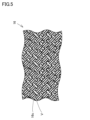
ここで、本実施の形態1に係るサーマルプリントヘッド1の特徴は、図4に示されるように、中空フィラ16cを含んだグレーズ層16が主面11上に配置されている点である。中空フィラ16cは、熱伝達率が低い領域Vを囲む粒状の部材である。中空フィラ16cの形状はたとえば球状である。中空フィラ16cを構成する材料は任意の材料を用いることができるが、たとえばガラスである。熱伝達率が低い領域Vに関して、たとえば、空気が当該領域Vに充填されていてもよい。当該領域Vの内部は特に真空であることが好ましい。
グレーズ層16は、発熱部31にて発生した熱の放熱を抑制し、当該サーマルプリントヘッド1の蓄熱性を向上させる。特に、グレーズ層16が前述した中空フィラ16cを含むことで、当該サーマルプリントヘッド1の蓄熱性が更に向上する。蓄熱性が向上することで、印刷媒体47に印字する際に流れる電流の量を低減することができる。
図5は、中空フィラ16cを含んだグレーズ層16の断面模式図である。図5に示されているように、グレーズ層16は中空フィラ16cを含んでいる。前述したように、中空フィラ16cは、中空の領域Vを含む。このような中空フィラ16cが、グレーズ層16内に点在している。中空フィラ16cが球状であれば、当該中空フィラ16cの直径は10μm以下であってもよく、1μm以下であることが好ましい。中空フィラ16cは小さければ、より多くの中空フィラ16cをグレーズ層16に含めることができる。そのため、グレーズ層16の空洞率(空気の領域あるいは真空の領域)が増加し、サーマルプリントヘッド1の蓄熱性が向上する。
異なる観点から言うと、サーマルプリントヘッド1の蓄熱性を向上させるために、グレーズ層16における中空フィラ16cの体積含有率は50%以上であってもよく、80%以上でもよく、90%以上がより好ましい。
前述したように、中空フィラ16cを構成する材料は、熱伝導率が低く、強度が確保できる材料であることが好ましい。また、後述する当該サーマルプリントヘッド1の製造中に熱により溶融しないために、中空フィラ16cを構成する材料は、融点が高い材料であることが好ましい。特に、中空フィラ16cを構成する材料の融点が800℃以上であることが好ましい。このような材料として、中空フィラ16cを構成する材料は、ガラスであることが好ましく、特に、石英ガラスがより好ましい。
図4に示されるように、サーマルプリントヘッド1の断面視において、グレーズ層16は、抵抗体層30と絶縁層15との間に配置されている。サーマルプリントヘッド1の蓄熱性を向上させるためには、抵抗体層30にて発生した熱が基板10に流れて放熱されることを抑制すればよい。そのため、グレーズ層16は抵抗体層30と基板10との間に配置されていればよい。たとえば、実施の形態2で後述するように、グレーズ層16は、基板10上に直接配置されてもよい。つまり、グレーズ層16は、絶縁層15と主面11との間に配置されてもよい(図15参照)。
z方向から見た主面11の平面視において、グレーズ層16は、主面11の凸部14の頂面14s1を覆うように配置されている。図4に示されるように、グレーズ層16は、y方向において、一対の傾斜面14s2に挟まれるように配置されている。
グレーズ層16は、第1グレーズ層16aと第2グレーズ層16bとを有する。中空フィラ16cは、第1グレーズ層16aに含まれる。第1グレーズ層16aは、絶縁層15に接続されている。第2グレーズ層16bは、第1グレーズ層16a上に配置されている。第2グレーズ層16bは、抵抗体層30に接続されている。
後述するように中空フィラ16cを含む第1グレーズ層16aを形成する際、流動性のあるグレーズを塗布する。そのため、図4に示されるようなサーマルプリントヘッド1の断面視において、頂面14s1と傾斜面14s2との交わる箇所は曲線で構成されていないことが好ましく、たとえば2本の直線が交わる角部となっていることが好ましい。このようにすることで、グレーズの表面張力を利用して、凸部14の頂面14s1にグレーズを搭載することができる。なお、上記のような角部を有する凸部14を形成するために、基板10を構成する材料は、シリコンであることが好ましい。その後、当該グレーズを乾燥させる。このようにして、中空フィラ16cを含む第1グレーズ層16aを形成することができる。
第2グレーズ層16bは、第1グレーズ層16a上に形成される。第2グレーズ層16bは、グレーズ印刷によって形成される。その後、焼成によって、グレーズ層16が形成される。このようにして形成されたグレーズ層16は、曲面部17を有する。曲面部17は、グレーズ層16において基板10からz方向に最も離れた面である。本実施の形態1に係るサーマルプリントヘッド1において、曲面部17は、抵抗体層30に接続されている面である。z方向からみた平面視において、曲面部17は、凸部14に重なっている。
グレーズ層16のz方向における厚みhは、たとえば、20μm以上250μm以下であり、頂面14s1のy方向における幅によって適宜変更可能である。厚みhが大きいほど、当該サーマルプリントヘッド1の蓄熱性が向上する。
(サーマルプリントヘッドの製造方法)
以下、本実施の形態のサーマルプリントヘッド1の製造方法を説明する。
以下、本実施の形態のサーマルプリントヘッド1の製造方法を説明する。
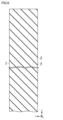
まず、ウエハ10aを準備する工程(S1a)が実施される。この工程(S1a)では、図6に示されるように、半導体材料であるシリコン基板としてのウエハ10aを準備する。ウエハ10aは、シリコンの単結晶を含む。
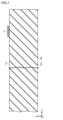
その次に、マスク層2を形成する工程(S2a)を実施する。この工程(S2a)では、図7に示されるように、主面11aにおいて凸部14を形成する領域にマスク層2を形成する。マスク層2を構成する材料は、たとえば、窒化珪素(SiN)または二酸化珪素(SiO2)である。マスク層2は、CVD法またはスパッタリングを用いて形成される。
その次に、エッチングする工程(S3a)を実施する。この工程(S3a)では、図8に示されるように、マスク層2をマスクとして用いてウエハ10aをウェットエッチングする。z方向からみた平面視において、マスク層2が配置されていない領域におけるウエハ10aが-z方向にエッチングされる。たとえば、水酸化カリウム(KOH)水溶液をエッチング液として、ウェットエッチングを実施する。このようにすることで、基板10が形成される。また、マスク層2が形成されている領域において、ウエハ10aはエッチングされない。そのため凸部14が基板10の主面11上に形成される。
エッチング液として水酸化カリウム(KOH)水溶液などのアルカリ性水溶液を用いた時、主面11に対する傾斜面14s2の傾斜角θが54.7°となるように、ウエハ10aがエッチングされる。図8に示される凸部14が形成された後、フッ化水素酸(HF)を用いたウェットエッチングによって、マスク層2を除去する。
次に、絶縁層15を形成する工程(S4a)を実施する。この工程(S4a)では、図9に示されるように、主面11の少なくとも一部と凸部14とを覆う絶縁層15を形成する。具体的には、絶縁層15は、熱酸化によって形成される。熱酸化によって形成された酸化膜の上に、プラズマCVD法を用いて、二酸化珪素の薄膜を複数回にわたって積層させることによってTEOS酸化膜が形成されてもよい。
次に、グレーズ層16を形成する工程(S5a)を実施する。この工程(S5a)では、図10に示されるように、絶縁層15上に、グレーズ層16を形成する。具体的には、中空フィラ16cが含まれたグレーズを、凸部14の頂面14s1に塗布する。その後、当該グレーズを乾燥させる。このようにして、中空フィラ16cを含む第1グレーズ層16aが形成される。
その後、第1グレーズ層16a上に、グレーズ印刷によってグレーズを塗布する。このようにして、第2グレーズ層16bが形成される。その後、焼成によって、グレーズ層16が形成される。
次に、抵抗体層30を形成する工程(S6a)を実施する。この工程(S6a)では、図11に示されるように、絶縁層15上に抵抗体層30を形成する。具体的には、抵抗体層30は、スパッタリングを用いて形成される。抵抗体層30を構成する材料は、たとえば、窒化タンタル(TaN)である。抵抗体層30を構成する材料は、ポリシリコンであってもよい。抵抗体層30は、複数の発熱部31を含む。
次に、配線層20を形成する工程(S7a)を実施する。この工程(S7a)では、図12に示されるように、抵抗体層30上に配線層20を形成する。具体的には、配線層20はスパッタリングを用いて形成される。配線層20は、たとえばスパッタリングを用いて、銅の薄膜を複数回にわたって積層して形成してもよい。スパッタリングを用いて、チタンの薄膜を抵抗体層30上に積層させた後、銅の薄膜を複数回にわたって積層して配線層20が形成されてもよい。配線層20は、チタンの薄膜および銅の薄膜を積層して形成されてなくてもよく、アルミニウムの薄膜を積層して配線層20が形成されてもよい。
配線層20を形成した後に、リソグラフィパターニングを施して、配線層20の一部を除去する。具体的には、配線層20上にフォトリソグラフィ法を用いてマスク層を形成する。当該マスク層をマスクとして配線層20を部分的にエッチングにより除去する。配線層20に対するエッチングとしては、ウェットエッチングを用いることができる。ウェットエッチングでは、硫酸(H2SO4)および過酸化水素(H2O2)の混合溶液を用いる。これにより、図3に示すように、共通配線21、および複数の個別配線25が、抵抗体層30の上に形成される。図12に示されるように、抵抗体層30の一部が配線層20から露出する。その次に、反応性イオンエッチングを用いて、抵抗体層30の一部をエッチングする。これによって、図3に示されるように凸部14上に絶縁層15が露出する。凸部14の頂面14s1上では、複数の発熱部31が露出する。
その次に、保護層33を形成する工程(S8a)を実施する。具体的には、図13に示されるように、絶縁層15上と、複数の発熱部31上と、配線層20の一部上とに、プラズマCVDを用いて保護層33を形成する。保護層33は、窒化珪素の薄膜を積層させることで形成される。配線層20のうち導電ワイヤ36,37がボンディングされる部分(例えば、端子部28など)は、保護層33から露出している。
次に、駆動回路35を実装する工程(S9a)を実施する。この工程(S9a)では、図14に示されるように、主面11上に駆動回路35を実装する。例えば、駆動回路35は、接着剤などの接合部材(図示せず)を用いて、絶縁層15に固定される。図14に示されるように、導電ワイヤ36,37をボンディングする。例えば、導電ワイヤ36は、ワイヤボンダ(図示せず)を用いて、駆動回路35と複数の個別配線25の端子部28とにボンディングされる。導電ワイヤ37は、ワイヤボンダ(図示せず)を用いて、駆動回路35と複数の引出配線29とにボンディングされる。
次に、封止する工程(S10a)を実施する。この工程(S10a)では、図15に示されるように、駆動回路35を封止部材43で封止する。例えば、駆動回路35上に封止樹脂材料をポッティングする。その後、封止樹脂材料を硬化させる。こうして、封止部材43が形成される。
次に、基板10にコネクタ40を取り付ける。コネクタ40は、複数のピン(図示せず)を含む。複数のピンの一部は、複数の引出配線29に導通している。複数のピンの別の一部は、共通配線21の基部22に導通する配線(図示せず)に導通している。
次に、基板10にヒートシンク49を取り付ける。具体的には、ヒートシンク49は、ねじのような締結部材または接合部材(図示せず)によって、基板10の裏面12に取り付けられる。こうして、図1から図4に示される本実施の形態のサーマルプリントヘッド1が得られる。
本実施の形態のサーマルプリントヘッド1の動作を説明する。
図1に示されるように、突起45は、サーマルプリンタに含まれるプラテンローラ46に対向している。プラテンローラ46は、印刷媒体47をサーマルプリントヘッド1に向けて送り出す。プラテンローラ46が回転することにより、印刷媒体47が+y方向に送り出される。突起45とプラテンローラ46との間に、印刷媒体47が挟み込まれる。
図1に示されるように、突起45は、サーマルプリンタに含まれるプラテンローラ46に対向している。プラテンローラ46は、印刷媒体47をサーマルプリントヘッド1に向けて送り出す。プラテンローラ46が回転することにより、印刷媒体47が+y方向に送り出される。突起45とプラテンローラ46との間に、印刷媒体47が挟み込まれる。
駆動回路35は、複数の個別配線25を通して、複数の発熱部31に個別に電流を印加する。複数の発熱部31のうち電流が印加された発熱部31が、選択的に発熱する。複数の発熱部31にて発生した熱は、印刷媒体47に伝わる。こうして、サーマルプリントヘッド1を用いて、印刷媒体47に印字が施される。グレーズ層16は、中空フィラ16cを含む。中空フィラ16cは、熱伝達率が低い真空領域Vを含む。そのため、複数の発熱部31にて発生した熱の一部は、グレーズ層16によって放熱が抑制される。複数の発熱部31にて発生した熱の残りは、基板10及びヒートシンク49を通して、サーマルプリントヘッド1の外部に放出される。
<作用効果>
本開示に従ったサーマルプリントヘッド1は、基板10とグレーズ層16とを備える。基板10は、主面11を有する。グレーズ層16は主面11上に配置されている。グレーズ層16は中空フィラ16cを含む。
本開示に従ったサーマルプリントヘッド1は、基板10とグレーズ層16とを備える。基板10は、主面11を有する。グレーズ層16は主面11上に配置されている。グレーズ層16は中空フィラ16cを含む。
このようにすれば、グレーズ層16が中空フィラ16cを含むことで、当該サーマルプリントヘッド1の蓄熱性が向上する。蓄熱性が向上することで、印刷媒体47に印字する際に流れる電流の量を低減することができる。
上記サーマルプリントヘッド1において、グレーズ層16における中空フィラ16cの体積含有率は50%以上である。このようにすれば、蓄熱性が十分向上したサーマルプリントヘッド1を得られる。蓄熱性が向上することで、印刷媒体47に印字する際に流れる電流の量を低減することができる。
上記サーマルプリントヘッド1において、中空フィラ16cはガラスを含む。このようにすれば、当該グレーズ層16の強度、および蓄熱性を確保することができる。また、サーマルプリントヘッド1の製造中に中空フィラ16cが熱により溶融することを抑制できる。
上記サーマルプリントヘッド1において、基板10を構成する材料はシリコンである。このようにすれば、水酸化カリウム(KOH)水溶液によるウェットエッチングを用いて凸部14を形成する際に、当該凸部14の断面視において凸部14が直線で構成されるようになる。その結果、表面張力を利用して、流動性のあるグレーズを頂面14s1に塗布することができる。
上記サーマルプリントヘッド1において、主面11には凸部14が形成されている。グレーズ層16は凸部14の頂面14s1を覆う。このようにすれば、発熱部31にて発生した熱が基板10に放熱することが抑制される。その結果、当該サーマルプリントヘッド1の蓄熱性が向上する。
上記サーマルプリントヘッド1において、グレーズ層16は曲面部17を有する。主面11に対して垂直な方向をz方向とする。z方向からみた平面視において、曲面部17は凸部14に重なっている。このようにすれば、凸部14上に発熱部31を形成することで発熱部31の表面を曲面状にすることができる。
上記サーマルプリントヘッド1において、グレーズ層16のz方向における厚みhは、20μm以上250μm以下である。このようにすることで、当該サーマルプリントヘッド1の蓄熱性が向上する。特に、厚みhが大きいほど、当該サーマルプリントヘッド1の蓄熱性が向上する。
上記サーマルプリントヘッド1は、絶縁層15と抵抗体層30とを更に備える。絶縁層15は主面11上に配置される。抵抗体層30は絶縁層15上に配置されている。グレーズ層16は、主面11と抵抗体層30との間に位置している。このようにすることで、抵抗体層30にて発生した熱が基板10に放熱することが抑制される。特に、発熱部31にて発生した熱が放熱することが抑制される。その結果、当該サーマルプリントヘッド1の蓄熱性が向上する。蓄熱性が向上することで、印刷媒体47に印字する際に流れる電流の量を低減することができる。
上記サーマルプリントヘッド1において、グレーズ層16は、抵抗体層30と絶縁層15との間に配置されている。このようにすることで、抵抗体層30にて発生した熱が基板10に放熱することが抑制される。特に、発熱部31にて発生した熱が放熱することが抑制される。
(実施の形態2)
図16は、実施の形態2のサーマルプリントヘッド1の概略部分拡大断面図である。図16は、図4に対応する。図16に示されたサーマルプリントヘッド1は、基本的には図1から図4に示されたサーマルプリントヘッド1と同様の構成を備え、同様の効果を得ることができるが、グレーズ層16が基板10上に直接配置されている点が図1から図4に示されたサーマルプリントヘッド1と異なる。つまり、グレーズ層16は、絶縁層15と主面11との間に配置されてもよい。このような構成によっても、蓄熱性が十分向上したサーマルプリントヘッド1を得られる。蓄熱性が向上することで、印刷媒体47に印字する際に流れる電流の量を低減することができる。
図16は、実施の形態2のサーマルプリントヘッド1の概略部分拡大断面図である。図16は、図4に対応する。図16に示されたサーマルプリントヘッド1は、基本的には図1から図4に示されたサーマルプリントヘッド1と同様の構成を備え、同様の効果を得ることができるが、グレーズ層16が基板10上に直接配置されている点が図1から図4に示されたサーマルプリントヘッド1と異なる。つまり、グレーズ層16は、絶縁層15と主面11との間に配置されてもよい。このような構成によっても、蓄熱性が十分向上したサーマルプリントヘッド1を得られる。蓄熱性が向上することで、印刷媒体47に印字する際に流れる電流の量を低減することができる。
(サーマルプリントヘッドの製造方法)
以下、本実施の形態2のサーマルプリントヘッド1の製造方法を説明する。
以下、本実施の形態2のサーマルプリントヘッド1の製造方法を説明する。
まず、実施の形態1に係るサーマルプリントヘッド1の製造方法における図6から図8に示された工程と同様の工程を実施する。すなわち、まずウエハ10aを準備する工程(S1b)が実施される。この工程(S1b)では、図6に示されるように、半導体材料であるシリコン基板としてのウエハ10aを準備する。ウエハ10aは、シリコンの単結晶を含む。
その次に、マスク層2を形成する工程(S2b)を実施する。この工程(S2b)では、図7に示されるように、主面11aにおいて凸部14を形成する領域にマスク層2を形成する。マスク層2を構成する材料は、たとえば、窒化珪素(SiN)または二酸化珪素(SiO2)である。マスク層2は、CVD法またはスパッタリングを用いて形成される。
その次に、エッチングする工程(S3b)を実施する。この工程(S3b)では、図8に示されるように、マスク層2をマスクとして用いてウエハ10aをウェットエッチングする。z方向からみた平面視において、マスク層2が配置されていない領域におけるウエハ10aが-z方向にエッチングされる。たとえば、水酸化カリウム(KOH)水溶液をエッチング液として、ウェットエッチングを実施する。このようにすることで、基板10が形成される。また、マスク層2が形成されている領域において、ウエハ10aはエッチングされない。そのため凸部14が基板10の主面11上に形成される。
エッチング液として水酸化カリウム(KOH)水溶液などのアルカリ性水溶液を用いた時、主面11に対する傾斜面14s2の傾斜角θが54.7°となるように、ウエハ10aがエッチングされる。図8に示される凸部14が形成された後、フッ化水素酸(HF)を用いたウェットエッチングによって、マスク層2を除去する。
次に、グレーズ層16を形成する工程(S4b)を実施する。この工程(S4b)では、図17に示されるように、基板10の頂面14s1上に、グレーズ層16を形成する。具体的には、中空フィラ16cが含まれたグレーズを、凸部14の頂面14s1に塗布する。その後、当該グレーズを乾燥させる。このようにして、中空フィラ16cを含む第1グレーズ層16aが形成される。
その後、第1グレーズ層16a上に、グレーズ印刷によってグレーズを塗布する。このようにして、第2グレーズ層16bが形成される。その後、焼成によって、グレーズ層16が形成される。
次に、絶縁層15を形成する工程(S5b)を実施する。この工程(S5a)では、図18に示されるように、主面11の少なくとも一部、凸部14の少なくとも一部、およびグレーズ層16上を覆う絶縁層15を形成する。具体的には、絶縁層15は、熱酸化によって形成される。熱酸化によって形成された酸化膜の上に、プラズマCVD法を用いて、二酸化珪素の薄膜を複数回にわたって積層させることによってTEOS酸化膜が形成されてもよい。
絶縁層15を形成する工程(S5b)の後に、図11~図15に示された抵抗体層30を形成する工程(S6a)から封止する工程(S10a)が順次実施される。このようにして、本実施の形態2に係るサーマルプリントヘッド1が製造される。
<作用効果>
上記サーマルプリントヘッド1において、グレーズ層16は、絶縁層15と主面11との間に配置されている。このようにすれば、蓄熱性が向上したサーマルプリントヘッド1を得られる。蓄熱性が向上することで、印刷媒体47に印字する際に流れる電流の量を低減することができる。
上記サーマルプリントヘッド1において、グレーズ層16は、絶縁層15と主面11との間に配置されている。このようにすれば、蓄熱性が向上したサーマルプリントヘッド1を得られる。蓄熱性が向上することで、印刷媒体47に印字する際に流れる電流の量を低減することができる。
以下、本開示の諸態様を付記としてまとめて記載する。
(付記1)
主面を有する基板と、
前記主面上に配置されたグレーズ層とを備え、
前記グレーズ層は中空フィラを含む、サーマルプリントヘッド。
(付記2)
前記中空フィラはガラスを含む、付記1に記載のサーマルプリントヘッド。
(付記3)
前記基板を構成する材料はシリコンである、付記1または付記2に記載のサーマルプリントヘッド。
(付記4)
前記主面には凸部が形成されており、
前記グレーズ層は前記凸部の頂面を覆う、付記3に記載のサーマルプリントヘッド。
(付記5)
前記グレーズ層は曲面部を有し、
前記主面に対して垂直な方向をz方向とすると、
前記z方向からみた平面視において、前記曲面部は前記凸部に重なっている、付記4に記載のサーマルプリントヘッド。
(付記6)
前記グレーズ層の前記z方向における厚みは、20μm以上250μm以下である、付記5に記載のサーマルプリントヘッド。
(付記7)
絶縁層と、
抵抗体層とを更に備え、
前記絶縁層は前記主面上に配置され、
前記抵抗体層は前記絶縁層上に配置され、
前記グレーズ層は、前記主面と前記抵抗体層との間に位置している、付記1から付記6のいずれか1項に記載のサーマルプリントヘッド。
(付記8)
前記グレーズ層は、前記抵抗体層と前記絶縁層との間に配置されている、付記7に記載のサーマルプリントヘッド。
(付記9)
前記グレーズ層は、前記絶縁層と前記主面との間に配置されている、付記7に記載のサーマルプリントヘッド。
(付記1)
主面を有する基板と、
前記主面上に配置されたグレーズ層とを備え、
前記グレーズ層は中空フィラを含む、サーマルプリントヘッド。
(付記2)
前記中空フィラはガラスを含む、付記1に記載のサーマルプリントヘッド。
(付記3)
前記基板を構成する材料はシリコンである、付記1または付記2に記載のサーマルプリントヘッド。
(付記4)
前記主面には凸部が形成されており、
前記グレーズ層は前記凸部の頂面を覆う、付記3に記載のサーマルプリントヘッド。
(付記5)
前記グレーズ層は曲面部を有し、
前記主面に対して垂直な方向をz方向とすると、
前記z方向からみた平面視において、前記曲面部は前記凸部に重なっている、付記4に記載のサーマルプリントヘッド。
(付記6)
前記グレーズ層の前記z方向における厚みは、20μm以上250μm以下である、付記5に記載のサーマルプリントヘッド。
(付記7)
絶縁層と、
抵抗体層とを更に備え、
前記絶縁層は前記主面上に配置され、
前記抵抗体層は前記絶縁層上に配置され、
前記グレーズ層は、前記主面と前記抵抗体層との間に位置している、付記1から付記6のいずれか1項に記載のサーマルプリントヘッド。
(付記8)
前記グレーズ層は、前記抵抗体層と前記絶縁層との間に配置されている、付記7に記載のサーマルプリントヘッド。
(付記9)
前記グレーズ層は、前記絶縁層と前記主面との間に配置されている、付記7に記載のサーマルプリントヘッド。
今回開示された実施の形態はすべての点で例示であって制限的なものではないと考えられるべきである。本開示の基本的な範囲は、上記した説明ではなく請求の範囲によって示され、請求の範囲と均等の意味および範囲内でのすべての変更が含まれることを意図される。
1 サーマルプリントヘッド、2 マスク層、10 基板、10a ウエハ、11,11a 主面、12,12a 裏面、14 凸部、14s1 頂面、14s2 傾斜面、15 絶縁層、16 金属層、16a 第1グレーズ層、16b 第2グレーズ層、16c 中空フィラ、17 曲面部、20 配線層、21 共通配線、22 基部、23,26 延出部、25 個別配線、27 端部、28 端子部、29 引出配線、30 抵抗体層、31 発熱部、33 保護層、35 駆動回路、36,37 導電ワイヤ、40 コネクタ、43 封止部材、45 突起、46 プラテンローラ、47 印刷媒体、49 ヒートシンク、h 厚み、V 領域。
Claims (9)
- 主面を有する基板と、
前記主面上に配置されたグレーズ層とを備え、
前記グレーズ層は中空フィラを含む、サーマルプリントヘッド。 - 前記中空フィラはガラスを含む、請求項1に記載のサーマルプリントヘッド。
- 前記基板を構成する材料はシリコンである、請求項1または請求項2に記載のサーマルプリントヘッド。
- 前記主面には凸部が形成されており、
前記グレーズ層は前記凸部の頂面を覆う、請求項3に記載のサーマルプリントヘッド。 - 前記グレーズ層は曲面部を有し、
前記主面に対して垂直な方向をz方向とすると、
前記z方向からみた平面視において、前記曲面部は前記凸部に重なっている、請求項4に記載のサーマルプリントヘッド。 - 前記グレーズ層の前記z方向における厚みは、20μm以上250μm以下である、請求項5に記載のサーマルプリントヘッド。
- 絶縁層と、
抵抗体層とを更に備え、
前記絶縁層は前記主面上に配置され、
前記抵抗体層は前記絶縁層上に配置され、
前記グレーズ層は、前記主面と前記抵抗体層との間に位置している、請求項1から請求項6のいずれか1項に記載のサーマルプリントヘッド。 - 前記グレーズ層は、前記抵抗体層と前記絶縁層との間に配置されている、請求項7に記載のサーマルプリントヘッド。
- 前記グレーズ層は、前記絶縁層と前記主面との間に配置されている、請求項7に記載のサーマルプリントヘッド。
Priority Applications (1)
| Application Number | Priority Date | Filing Date | Title |
|---|---|---|---|
| JP2025533897A JPWO2025018043A1 (ja) | 2023-07-14 | 2024-06-03 |
Applications Claiming Priority (2)
| Application Number | Priority Date | Filing Date | Title |
|---|---|---|---|
| JP2023-115786 | 2023-07-14 | ||
| JP2023115786 | 2023-07-14 |
Publications (1)
| Publication Number | Publication Date |
|---|---|
| WO2025018043A1 true WO2025018043A1 (ja) | 2025-01-23 |
Family
ID=94281737
Family Applications (1)
| Application Number | Title | Priority Date | Filing Date |
|---|---|---|---|
| PCT/JP2024/020147 Pending WO2025018043A1 (ja) | 2023-07-14 | 2024-06-03 | サーマルプリントヘッド |
Country Status (2)
| Country | Link |
|---|---|
| JP (1) | JPWO2025018043A1 (ja) |
| WO (1) | WO2025018043A1 (ja) |
Citations (3)
| Publication number | Priority date | Publication date | Assignee | Title |
|---|---|---|---|---|
| JPH08192526A (ja) * | 1994-11-18 | 1996-07-30 | Fuji Photo Film Co Ltd | サーマルヘッド及びその製造方法 |
| JP2021011021A (ja) * | 2019-07-03 | 2021-02-04 | ローム株式会社 | サーマルプリントヘッドおよびその製造方法 |
| JP2022125740A (ja) * | 2021-02-17 | 2022-08-29 | ローム株式会社 | 蓄熱層の形成方法、サーマルプリントヘッド及びその製造方法、並びにサーマルプリンタ |
-
2024
- 2024-06-03 JP JP2025533897A patent/JPWO2025018043A1/ja active Pending
- 2024-06-03 WO PCT/JP2024/020147 patent/WO2025018043A1/ja active Pending
Patent Citations (3)
| Publication number | Priority date | Publication date | Assignee | Title |
|---|---|---|---|---|
| JPH08192526A (ja) * | 1994-11-18 | 1996-07-30 | Fuji Photo Film Co Ltd | サーマルヘッド及びその製造方法 |
| JP2021011021A (ja) * | 2019-07-03 | 2021-02-04 | ローム株式会社 | サーマルプリントヘッドおよびその製造方法 |
| JP2022125740A (ja) * | 2021-02-17 | 2022-08-29 | ローム株式会社 | 蓄熱層の形成方法、サーマルプリントヘッド及びその製造方法、並びにサーマルプリンタ |
Also Published As
| Publication number | Publication date |
|---|---|
| JPWO2025018043A1 (ja) | 2025-01-23 |
Similar Documents
| Publication | Publication Date | Title |
|---|---|---|
| US11458739B2 (en) | Thermal print head, manufacturing method of thermal print head, and thermal printer | |
| CN110509672B (zh) | 热敏打印头 | |
| WO2025018043A1 (ja) | サーマルプリントヘッド | |
| US11850870B2 (en) | Thermal print head and manufacturing method thereof | |
| US20220063292A1 (en) | Thermal print head, manufacturing method of thermal print head, and thermal printer | |
| JP2024154531A (ja) | サーマルプリントヘッド | |
| US11926156B2 (en) | Thermal print head and method of fabricating thereof | |
| JP2023072582A (ja) | サーマルプリントヘッド、およびサーマルプリントヘッドの製造方法 | |
| WO2021200401A1 (ja) | サーマルプリントヘッド、およびサーマルプリントヘッドの製造方法 | |
| JP2024024913A (ja) | サーマルプリントヘッドおよびサーマルプリンタ | |
| JP2023165460A (ja) | サーマルプリントヘッド | |
| JP2023167832A (ja) | サーマルプリントヘッド、およびサーマルプリントヘッドの製造方法 | |
| JP2025187072A (ja) | サーマルプリントヘッド | |
| JP7569680B2 (ja) | サーマルプリントヘッド、およびサーマルプリントヘッドの製造方法 | |
| WO2024014066A1 (ja) | サーマルプリントヘッド | |
| JP2024009481A (ja) | サーマルプリントヘッドおよびサーマルプリントヘッドの製造方法 | |
| JP7557320B2 (ja) | サーマルプリントヘッド | |
| JP2023121929A (ja) | サーマルプリントヘッド | |
| US11633959B2 (en) | Thermal print head | |
| JP2023128840A (ja) | サーマルプリントヘッド | |
| JP2023072897A (ja) | サーマルプリントヘッド、およびサーマルプリントヘッドの製造方法 | |
| JP2023109032A (ja) | サーマルプリントヘッド、およびサーマルプリントヘッドの製造方法 | |
| JP2024009569A (ja) | サーマルプリントヘッド及びその製造方法 | |
| CN114728523B (zh) | 热敏打印头及其制造方法 | |
| JP2025065724A (ja) | サーマルプリントヘッド |
Legal Events
| Date | Code | Title | Description |
|---|---|---|---|
| 121 | Ep: the epo has been informed by wipo that ep was designated in this application |
Ref document number: 24842839 Country of ref document: EP Kind code of ref document: A1 |
|
| ENP | Entry into the national phase |
Ref document number: 2025533897 Country of ref document: JP Kind code of ref document: A |
|
| WWE | Wipo information: entry into national phase |
Ref document number: 2025533897 Country of ref document: JP |
|
| NENP | Non-entry into the national phase |
Ref country code: DE |