WO2025018024A1 - 電波反射装置の検査方法 - Google Patents
電波反射装置の検査方法 Download PDFInfo
- Publication number
- WO2025018024A1 WO2025018024A1 PCT/JP2024/018825 JP2024018825W WO2025018024A1 WO 2025018024 A1 WO2025018024 A1 WO 2025018024A1 JP 2024018825 W JP2024018825 W JP 2024018825W WO 2025018024 A1 WO2025018024 A1 WO 2025018024A1
- Authority
- WO
- WIPO (PCT)
- Prior art keywords
- radio wave
- light
- wave reflecting
- voltage
- reflecting device
- Prior art date
- Legal status (The legal status is an assumption and is not a legal conclusion. Google has not performed a legal analysis and makes no representation as to the accuracy of the status listed.)
- Ceased
Links
Images







Classifications
-
- H—ELECTRICITY
- H01—ELECTRIC ELEMENTS
- H01Q—ANTENNAS, i.e. RADIO AERIALS
- H01Q15/00—Devices for reflection, refraction, diffraction or polarisation of waves radiated from an antenna, e.g. quasi-optical devices
- H01Q15/14—Reflecting surfaces; Equivalent structures
-
- H—ELECTRICITY
- H01—ELECTRIC ELEMENTS
- H01Q—ANTENNAS, i.e. RADIO AERIALS
- H01Q15/00—Devices for reflection, refraction, diffraction or polarisation of waves radiated from an antenna, e.g. quasi-optical devices
- H01Q15/24—Polarising devices; Polarisation filters
-
- H—ELECTRICITY
- H01—ELECTRIC ELEMENTS
- H01Q—ANTENNAS, i.e. RADIO AERIALS
- H01Q3/00—Arrangements for changing or varying the orientation or the shape of the directional pattern of the waves radiated from an antenna or antenna system
- H01Q3/44—Arrangements for changing or varying the orientation or the shape of the directional pattern of the waves radiated from an antenna or antenna system varying the electric or magnetic characteristics of reflecting, refracting, or diffracting devices associated with the radiating element
Definitions
- the present invention relates to a method for inspecting radio wave reflecting devices.
- Radio wave reflecting devices are used to deliver radio waves to areas where radio waves have difficulty reaching (dead zones), such as the gaps between tall buildings.
- Examples of radio wave reflecting devices that have been disclosed include a configuration in which a main array element (dipole element), a subarray element (unpowered element), and a common electrode (ground electrode) are arranged with a dielectric substrate between them, with the subarray element arranged close to the main array element (Patent Document 1), and a configuration in which the array element and the common electrode (ground electrode) sandwich a dielectric substrate, with the common electrode having a periodic loop shape (Patent Document 2).
- a dielectric substrate is used in radio wave reflecting devices, but if the part equivalent to this dielectric substrate is replaced with a liquid crystal layer, the dielectric anisotropy of the liquid crystal material can be utilized, making it possible to vary the directionality of the reflected waves.
- Radio wave reflecting devices using liquid crystal material have a configuration in which reflecting elements are arranged in a matrix, similar to a planar array antenna in which a patch array is arranged. Radio wave reflecting devices control the direction of radio wave reflection by changing the dielectric constant of the liquid crystal layer that forms each reflecting element by applying a voltage between the electrodes. Therefore, to determine whether a radio wave reflecting device is good or bad, it is necessary to inspect the operation of each reflecting element.
- radio wave reflecting devices using liquid crystal have the problem that inspecting the quality of each reflecting element individually takes a lot of time, resulting in reduced productivity.
- one embodiment of the present invention aims to provide an inspection method that can determine the quality of the reflecting elements of a radio wave reflecting device by observing the entire surface at once.
- the method for inspecting a radio wave reflecting device is a method for inspecting a radio wave reflecting device having a plurality of reflecting elements arranged in row and column directions, each of which has a patch electrode, a common electrode overlapping the rear side of the patch electrode, and a liquid crystal layer between the plurality of patch electrodes and the common electrode, and which constitutes a radio wave reflector.
- a light source located above the radio wave reflecting device irradiates the radio wave reflecting device with a first light through a first polarizing plate, and an imaging device located above the radio wave reflecting device captures an image of the radio wave reflecting plate through a second polarizing plate having a transmission axis perpendicular to the transmission axis of the first polarizing plate, and the quality of the reflecting elements is judged based on the presence or absence of a second light reflected by the radio wave reflecting plate of the first light in the image.
- FIG. 5A to 5C are cross-sectional views for explaining a method for inspecting a radio wave reflecting device according to one embodiment of the present invention.
- FIG. 2 is a plan view for explaining a method for inspecting a radio wave reflecting device according to an embodiment of the present invention.
- FIG. 2 is a plan view for explaining a method for inspecting a radio wave reflecting device according to an embodiment of the present invention.
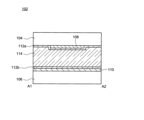
- FIG. 1A and 1B show a reflecting element 102 used in a radio wave reflecting device 100 according to one embodiment of the present invention.
- Fig. 1A shows a plan view of the reflecting element 102 as viewed from above (the side where radio waves are incident), and
- Fig. 1B shows a cross-sectional view between A1 and A2 shown in the plan view.
- the reflective element 102 includes a dielectric substrate 104, a counter substrate 106, a patch electrode 108, a common electrode 110, a first alignment film 112a, a second alignment film 112b, and a liquid crystal layer 114.
- the dielectric substrate 104 can be regarded as a dielectric layer, forming one layer.
- the patch electrode 108 is provided on the dielectric substrate 104
- the common electrode 110 is provided on the counter substrate 106.
- the common electrode 110 is disposed on the rear side of the patch electrode 108.
- a first alignment film 112a is provided on the dielectric substrate 104 so as to cover the patch electrode 108, and a second alignment film 112b is provided on the counter substrate 106 so as to cover the common electrode 110.
- the patch electrode 108 and the common electrode 110 are disposed so as to face each other, and a liquid crystal layer 114 is provided between them.
- a first alignment film 112a is interposed between the patch electrode 108 and the liquid crystal layer 114
- a second alignment film 112b is interposed between the common electrode 110 and the liquid crystal layer 114.
- the patch electrode 108 preferably has a shape that is symmetrical with respect to the vertically polarized and horizontally polarized waves of the incident radio wave, and has, for example, a square or circular shape in a plan view. However, this is merely a preferred example, and the shape is not limited to this.
- FIG. 1A shows a case where the patch electrode 108 is square in a plan view.
- the shape of the common electrode 110 There is no particular limitation on the shape of the common electrode 110, and it has a shape that spreads over almost the entire surface of the opposing substrate 106 so as to have an area larger than that of the patch electrode 108.
- the material that forms the patch electrode 108 and the common electrode 110 are formed using conductive metals and metal oxides.
- the dielectric substrate 104 may be provided with a first wiring 118.
- the first wiring 118 is connected to the patch electrode 108.
- the first wiring 118 can be used when applying a control signal to the patch electrode 108.
- the first wiring 118 can be used when connecting a patch electrode to an adjacent patch electrode.
- the dielectric substrate 104 and the opposing substrate 106 are bonded together by a sealant.
- the dielectric substrate 104 and the opposing substrate 106 are disposed opposite each other with a gap therebetween, and the liquid crystal layer 114 is provided within the area surrounded by the sealant.
- the liquid crystal layer 114 is provided so as to fill the gap between the dielectric substrate 104 and the opposing substrate 106.
- the gap between the dielectric substrate 104 and the opposing substrate 106 is 20 to 100 ⁇ m, for example, 50 ⁇ m.
- a patch electrode 108, a common electrode 110, a first alignment film 112a, and a second alignment film 112b are provided between the dielectric substrate 104 and the opposing substrate 106, so that to be precise, the gap between the first alignment film 112a and the second alignment film 112b provided on each of the dielectric substrate 104 and the opposing substrate 106 is the thickness of the liquid crystal layer 114.
- a spacer may be provided between the dielectric substrate 104 and the opposing substrate 106 to maintain a constant distance.
- the liquid crystal layer 114 having dielectric anisotropy has a dielectric constant that changes with the change in the orientation state of the liquid crystal molecules.
- the reflecting element 102 can change the dielectric constant of the liquid crystal layer 114 by the control signal applied to the patch electrode 108, and can thereby delay the phase of the reflected wave when reflecting the radio wave.
- the frequency bands of radio waves reflected by the reflective element 102 are the very high frequency (VHF) band, the ultra high frequency (UHF) band, the super high frequency (SHF) band, the submillimeter wave (THF: tremendous high frequency) band, and the millimeter wave (EHF: extra high frequency) band.
- VHF very high frequency
- UHF ultra high frequency
- SHF super high frequency
- THF very high frequency
- EHF millimeter wave
- the orientation of the liquid crystal molecules in the liquid crystal layer 114 changes in response to a control signal applied to the patch electrode 108, but does not follow the frequency of the radio waves irradiated to the patch electrode 108 at all. Therefore, the reflective element 102 can control the phase of the reflected radio waves without being affected by the radio waves.
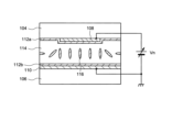
- FIG. 2A shows a state where no voltage is applied between the patch electrode 108 and the common electrode 110 (referred to as the "first state”).
- FIG. 2A shows a case where the first alignment film 112a and the second alignment film 112b are horizontal alignment films. In the first state, the long axes of the liquid crystal molecules 116 are aligned horizontally to the surfaces of the patch electrode 108 and the common electrode 110 by the first alignment film 112a and the second alignment film 112b.
- FIG. 2B shows a state where a control signal (voltage signal) is applied to the patch electrode 108 (referred to as the "second state").
- the liquid crystal molecules 116 are oriented with their long axes perpendicular to the surfaces of the patch electrode 108 and the common electrode 110 under the action of an electric field.
- the angle at which the long axes of the liquid crystal molecules 116 are aligned can also be aligned in a direction intermediate between the horizontal and vertical directions depending on the magnitude of the control signal applied to the patch electrode 108 (the magnitude of the voltage Vn between the common electrode and the patch electrode).
- the dielectric constant is greater in the second state than in the first state.
- the liquid crystal molecules 116 have negative dielectric anisotropy, if they are vertically aligned in advance, the apparent dielectric constant is greater in the second state than in the first state, and when the liquid crystal molecules 116 are horizontally aligned, the apparent dielectric constant is already high, so that the orientation does not change significantly from the horizontal alignment even when an electric field is applied.
- the liquid crystal layer 114 which has dielectric anisotropy, can also be considered as a variable dielectric layer.
- the reflective element 102 can utilize the dielectric anisotropy of the liquid crystal layer 114 to control the phase of the reflected wave to be delayed (or not delayed).
- the reflecting element 102 is used in a radio wave reflector that reflects radio waves in a specified direction. It is preferable that the reflecting element 102 attenuates the amplitude of the reflected radio waves as little as possible. As is clear from the structure shown in FIG. 1B, when radio waves propagating through the air are reflected by the reflecting element 102, the radio waves pass through the dielectric substrate 104 twice.
- the dielectric substrate 104 is formed of a dielectric material such as glass or resin.
- Radio Wave Reflecting Device Next, the structure of a radio wave reflecting device in which reflecting elements are integrated will be shown.
- Radio wave reflection device A (single-axis reflection control) 3 shows a configuration of a radio wave reflecting device 100a according to an embodiment of the present invention.
- the radio wave reflecting device 100 has a radio wave reflecting plate 120.
- the radio wave reflecting plate 120 is composed of a plurality of reflecting elements 102.
- the plurality of reflecting elements 102 are arranged, for example, in a column direction (X-axis direction shown in FIG. 3) and a column direction (Y-axis direction shown in FIG. 3) intersecting the column direction.
- the reflecting elements 102 are arranged so that the patch electrodes 108 face the radio wave incident surface.
- the radio wave reflecting plate 120 is flat, and a plurality of patch electrodes 108 are arranged in a matrix on the flat surface.
- the radio wave reflecting device 100a has a structure in which a plurality of reflecting elements 102 are integrated on one dielectric substrate 104. As shown in FIG. 3, the radio wave reflecting device 100 has a structure in which a dielectric substrate 104 on which a plurality of patch electrodes 108 are arranged and an opposing substrate 106 on which a common electrode 110 is provided are arranged in layers, and a liquid crystal layer (not shown) is provided between the two substrates.
- the radio wave reflecting plate 120 is formed in the area where the plurality of patch electrodes 108 and the common electrode 110 overlap.
- the cross-sectional structure of the radio wave reflecting plate 120 is the same as the structure of the reflecting element 102 shown in FIG. 1B when viewed from the perspective of each patch electrode 108.
- the dielectric substrate 104 and the opposing substrate 106 are bonded together with a sealant 128, and a liquid crystal layer (not shown) is provided in the area inside the sealant 128.
- the dielectric substrate 104 has a region facing the opposing substrate 106, as well as a peripheral region 122 extending outward from the opposing substrate 106.
- a first drive circuit 124 and a terminal section 126 are provided in the peripheral region 122.
- the first drive circuit 124 outputs a control signal to the patch electrode 108.
- the terminal section 126 is a region for forming a connection with an external circuit, and is connected to, for example, a flexible printed circuit board (FPC) (not shown).
- FPC flexible printed circuit board
- a plurality of patch electrodes 108 are arranged in the column direction (X-axis direction) and the row direction (Y-axis direction) on the dielectric substrate 104.
- a plurality of first wirings 118 extending in the column direction (Y-axis direction) are also arranged on the dielectric substrate 104.
- Each of the plurality of first wirings 118 is electrically connected to the plurality of patch electrodes 108 arranged in the column direction (Y-axis direction).
- the plurality of patch electrodes 108 arranged in the column direction (Y-axis direction) are connected by the first wirings 118.
- the radio wave reflector 120 has a configuration in which a row of patch electrode arrays connected by the first wirings 118 are arranged in the column direction (X-axis direction).
- the multiple first wirings 118 arranged on the radio wave reflecting plate 120 extend into the peripheral region 122 and are connected to the first driving circuit 124.
- the first driving circuit 124 is capable of outputting control signals of different voltage levels to each of the multiple first wirings 118.
- a control signal is applied to each of the multiple patch electrodes 108 arranged in the column direction (X-axis direction) and column direction (Y-axis direction) for each column (each patch electrode 108 arranged in the column direction (Y-axis direction)).
- a control signal is applied to each set of multiple patch electrodes 108 arranged in the column direction (Y-axis direction), thereby controlling the reflection direction of the reflected wave of the radio wave incident on the radio wave reflector 120.
- the radio wave reflecting device 100a can control the propagation direction of the reflected wave of the radio wave irradiated to the radio wave reflector 120 in the left-right direction of the drawing, centered on the reflection axis VR parallel to the column direction (Y-axis direction).
- Figure 4 shows a schematic diagram of how the direction of reflected waves changes depending on the two reflecting elements 102.
- different control signals V1 ⁇ V2
- V1 ⁇ V2 different control signals
- the phase change of the reflected wave by reflecting element 102b is greater than that of reflecting element 102a.
- the phase of reflected wave R1 reflected by reflecting element 102a differs from the phase of reflected wave R2 reflected by reflecting element 102b (in Figure 4, the phase of reflected wave R2 leads the phase of reflected wave R1), and the apparent direction of reflected wave changes obliquely.
- Radio wave reflection device B (two-axis reflection control)
- the radio wave reflecting device 100a shown in Fig. 3 has a single reflection axis VR, so the reflection angle can be controlled in the direction around the reflection axis VR as the rotation axis.
- this embodiment shows an example of a radio wave reflecting device 100b that can perform two-axis reflection control. The following description will focus on the differences from the radio wave reflecting device 100a.
- the radio wave reflecting device 100b has a plurality of second wirings 132 extending in the row direction (X-axis direction).
- the plurality of first wirings 118 and the plurality of second wirings 132 are arranged to intersect with an insulating layer (not shown) between them.
- the plurality of first wirings 118 are connected to a first drive circuit 124, and the plurality of second wirings 132 are connected to a second drive circuit 130.
- the second drive circuit 130 outputs a scanning signal.
- FIG. 5B shows an enlarged view of the arrangement 102m of the four patch electrodes 108 and the two first wirings 118 and second wirings 132.
- a switching element 134 is provided on each of the four patch electrodes 108. The switching (on and off) of the switching element 134 is controlled by a scanning signal applied to the second wiring 132. When the switching element 134 is turned on, the patch electrode 108 is conductive with the first wiring 118 and a control signal is applied to it.
- the switching element 134 is formed of, for example, a thin film transistor. With this configuration, a plurality of patch electrodes 108 arranged in the row direction (X-axis direction) can be selected for each row, and control signals of different voltage levels can be applied to each row.
- the radio wave reflecting device 100b shown in FIG. 5A can control the direction of travel of the reflected wave irradiated to the radio wave reflector 120 in the left-right direction of the drawing, centered on a reflection axis VR parallel to the column direction (Y-axis direction), and can also control the direction of travel of the reflected wave in the up-down direction of the drawing, centered on a reflection axis HR parallel to the column direction (X-axis direction).
- the radio wave reflecting device 100b has a reflection axis VR parallel to the column direction (Y-axis direction) and a reflection axis HR parallel to the column direction (X-axis direction), it can control the reflection angle in the direction about the reflection axis VR as the rotation axis and in the direction about the reflection axis HR as the rotation axis.
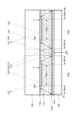
- FIG. 6 shows an example of a cross-sectional structure of a reflective element 102 in which a switching element 134 is connected to a patch electrode 108.
- the switching element 134 is provided on the dielectric substrate 104.
- the switching element 134 is a transistor and has a structure in which a first gate electrode 138, a first gate insulating layer 140, a semiconductor layer 142, a second gate insulating layer 146, and a second gate electrode 148 are stacked.
- An undercoat layer 136 may be provided between the first gate electrode 138 and the dielectric substrate 104.
- a first wiring 118 is provided between the first gate insulating layer 140 and the second gate insulating layer 146. The first wiring 118 is provided so as to contact the semiconductor layer 142.
- a first connection wiring 144 is provided in the same layer as the conductive layer that forms the first wiring 118.
- the first connection wiring 144 is provided so as to contact the semiconductor layer 142.
- the connection structure of the first wiring 118 and the first connection wiring 144 to the semiconductor layer 142 shows a structure in which one wiring is connected to the source of the transistor and the other wiring is connected to the drain.
- a first interlayer insulating layer 150 is provided so as to cover the switching element 134.
- a second wiring 132 is provided on the first interlayer insulating layer 150.
- the second wiring 132 is connected to the second gate electrode 148 through a contact hole formed in the first interlayer insulating layer 150.
- the first gate electrode 138 and the second gate electrode 148 are electrically connected to each other in a region that does not overlap with the semiconductor layer 142.
- a second connection wiring 152 is provided on the first interlayer insulating layer 150 using the same conductive layer as the second wiring 132.
- the second connection wiring 152 is connected to the first connection wiring 144 through a contact hole formed in the first interlayer insulating layer 150.
- a second interlayer insulating layer 154 is provided to cover the second wiring 132 and the second connection wiring 152. Furthermore, a planarizing layer 156 is provided to fill the step of the switching element 134. By providing the planarizing layer 156, the patch electrode 108 can be formed without being affected by the arrangement of the switching element 134.
- a passivation layer 158 is provided on the flat surface of the planarizing layer 156. The patch electrode 108 is provided on the passivation layer 158. The patch electrode 108 is connected to the second connection wiring 152 via a contact hole that penetrates the passivation layer 158, the planarizing layer 156, and the second interlayer insulating layer 154.
- a first alignment film 112a is provided on the patch electrode 108.
- the opposing substrate 106 is provided with a common electrode 110 and a second alignment film 112b, as in FIG. 1B.
- the surface of the dielectric substrate 104 on which the switching element 134 and the patch electrode 108 are provided faces the surface of the opposing substrate on which the common electrode 110 is provided, and a liquid crystal layer 114 is provided therebetween.
- the thickness T of the dielectric substrate 104 can be the length from the surface of the patch electrode 108 on the liquid crystal layer 114 side to the surface of the dielectric substrate 104 opposite to the surface on which the patch electrode 108 is provided.
- the thickness of at least one insulating layer (undercoat layer 136, first gate insulating layer 140, second gate insulating layer 146, first interlayer insulating layer 150, second interlayer insulating layer 154, planarization layer 156, passivation layer 158) between the patch electrode 108 and the dielectric substrate 104 can be taken into consideration.
- the undercoat layer 136 is formed, for example, of a silicon oxide film.
- the first gate insulating layer 140 and the second gate insulating layer 146 are formed, for example, of a silicon oxide film or a laminated structure of a silicon oxide film and a silicon nitride film.
- the semiconductor layer is formed of an oxide semiconductor including a silicon semiconductor such as amorphous silicon or polycrystalline silicon, and a metal oxide such as indium oxide, zinc oxide, or gallium oxide.
- the first gate electrode 138 and the second gate electrode 148 may be composed of, for example, molybdenum (Mo), tungsten (W), or an alloy thereof.
- the first wiring 118, the second wiring 132, the first connection wiring 144, and the second connection wiring 152 are formed using a metal material such as titanium (Ti), aluminum (Al), or molybdenum (Mo).
- a metal material such as titanium (Ti), aluminum (Al), or molybdenum (Mo).
- it may be configured with a titanium (Ti)/aluminum (Al)/titanium (Ti) laminated structure, or a molybdenum (Mo)/aluminum (Al)/molybdenum (Mo) laminated structure.
- the planarization layer 156 is formed of a resin material such as acrylic or polyimide.
- the passivation layer 158 is formed of, for example, a silicon nitride film.
- the patch electrode 108 and the common electrode 110 are formed of a metal film such as aluminum (Al) or copper (Cu).
- a control signal can be applied to a specific patch electrode selected from the multiple patch electrodes 108 arranged in a matrix.
- a control voltage can be applied to each patch electrode 108 arranged in a horizontal row along the first direction (X-axis direction) or each patch electrode 108 arranged in a vertical row along the second direction (Y-axis direction). For example, when the radio wave reflector 120 is upright, the reflection direction of the reflected wave can be controlled in the left-right and up-down directions.
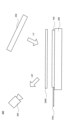
- the inspection device 200 basically comprises a light source 202, an image capture device 204, a sample stage 206, and a polarizing plate 208.
- Figure 7 is a cross-sectional view of an inspection device used to inspect a radio wave reflecting device according to one embodiment of the present invention.
- the light source 202 has an irradiation area capable of irradiating the entire surface of the radio wave reflecting device 100 (the entire surface of the radio wave reflecting plate 120) with, for example, white light.
- the light source 202 is arranged diagonally above the sample stage 206.
- the imaging device 204 is arranged so that the light emitted from the light source 202 does not directly enter.
- the light source 202 is arranged so that when the radio wave reflecting device 100 is installed on the sample stage 206, the light emitted from the light source 202 irradiates the entire radio wave reflecting plate 120 of the radio wave reflecting device 100.
- the radio wave reflecting device 100 is installed on the sample stage 206 so that the light emitted from the light source 202 is incident on the radio wave reflecting plate 120 on which the patch electrodes 108 are arranged. Since the patch electrodes 108 are formed of metal, the light source 202 is arranged diagonally above so that the light source 202 is not reflected in the radio wave reflecting plate 120 when the radio wave reflecting device 100 is placed on the sample stage 206.
- the light source 202 can be, for example, a surface-illuminating light source in which the light of a halogen lamp is guided by a light guide, or a surface light source using a white LED or fluorescent lamp.
- the imaging device 204 images the light LY emitted from the light source 202 through the polarizing plate 208 and reflected by the radio wave reflecting plate 120 through the polarizing plate 208.
- the imaging device 204 is located above the sample stage 206, and is disposed at a position where the light reflected by the radio wave reflecting plate 120 is incident.
- the imaging device 204 has a viewing angle that can capture the entire surface of the radio wave reflecting plate 120 as a single image.
- a camera such as a digital camera or a video camera can be used as the imaging device 204.
- the imaging device 204 captures the entire surface of the radio wave reflecting plate 120 on which the patch electrodes 108 are arranged in a single image, thereby shortening the time required to observe the entire radio wave reflecting device 100.
- the imaging device 204 was mentioned above, the image of the light LY emitted from the light source 202 through the polarizing plate 208 and reflected by the radio wave reflector 120 may actually be visually confirmed.
- the sample stage 206 has a flat surface so that the radio wave reflecting device 100 can be stably held.
- the sample stage 206 may be equipped with a fixing member for fixing the radio wave reflecting device 100, a vacuum chuck, etc.
- the polarizing plate 208 is a linear polarizing plate that transmits light of one polarized component of the light emitted from the light source 202. Therefore, linearly polarized light is illuminated on the radio wave reflecting device 100.
- the polarizing plate 208 is arranged on the light source 202 side and the imaging device 204 side. Specifically, as shown in FIG. 7, the polarizing plate 208-1 is arranged between the radio wave reflecting device 100 and the light source 202, and the polarizing plate 208-2 is arranged between the imaging device 204.
- the polarizing plates 208-1 and 208-2 are arranged so that their transmission axes are perpendicular (crossed Nicol). As shown in FIG.
- the transmission axis TA1 of the polarizing plate 208-1 and the transmission axis TA2 of the polarizing plate 208-2 are perpendicular.
- the direction in which the liquid crystal molecules 116 of the radio wave reflecting device 100 are oriented in the first state shown in FIG. 2A and the polarization direction emitted through the polarizing plate 208-1 are parallel or perpendicular.
- Polarizing plate 208-1 and polarizing plate 208-2 are not arranged facing each other, but are arranged so that they face toward radio wave reflecting device 100 or sample stage 206, respectively.
- the imaging device 204 does not directly receive the light emitted from the light source 202 to capture an image, but receives the linearly polarized component LY whose polarization state has not been maintained by the liquid crystal layer 114 to capture an image.
- the inspection device 200 of this embodiment uses such characteristics of the liquid crystal layer 114 to inspect the quality of the reflection element 102 that forms the radio wave reflector 120 (whether it is a good product that operates normally or a defective product that does not operate).
- FIG. 7 shows an example in which the inspection device 200 is configured with two linear polarizing plates, but the configuration of the polarizing plates is not limited to this example.
- a polarizing plate combining a linear polarizing plate and a quarter-wave plate for example a circular polarizing plate
- the inspection device 200 can be configured with a single polarizing plate.
- a polarizing plate 208C circular polarizing plate
- the polarizing plate 208C can polarize the light LV emitted from the light source 202, remove the polarized light that is specularly reflected by the radio wave reflecting device 100, and transmit the other light (light LW).
- the polarizing plate 208C is preferably large enough to cover the radio wave reflecting device 100 or the radio wave reflecting plate 120.
- the radio wave reflecting device 100 is placed on the inspection device 200 so that it can be observed from above, with the direction in which the patch electrode 108 can be observed being the upper surface.
- the radio wave reflecting device 100 is placed on the sample stage 206 of the inspection device so that the patch electrode 108 of the reflecting element 102 is on the light source 202 and imaging device 204 side, and the common electrode 110 is on the sample stage 206 side.
- voltages V0 to V2 are applied between the patch electrode 108 and the common electrode 110, and light is irradiated from the light source 202 to the radio wave reflecting device 100 through the polarizing plate 208-1.
- voltage V0 indicates that the voltage between the patch electrode 108 and the common electrode 110 is 0V, and the application of 0V is also included in the application of voltages.
- Voltages V0 to V2 are different from each other.
- the absolute values of voltages V0 to V2 are larger in the order of voltage V0, voltage V1, and voltage V2.
- the order of applying a voltage between the patch electrode 108 and the common electrode 110 and irradiating the radio wave reflecting device 100 with light does not need to be as described above.
- light may be irradiated onto the radio wave reflecting device 100 before applying a voltage between the patch electrode 108 and the common electrode 110.
- the imaging device 204 is used to capture an image of the radio wave reflector 120 so that the entire surface of the radio wave reflector 120 fits into a single image. At this time, the radio wave reflector 120 is captured through the polarizing plate 208-2.
- the quality of the reflective element 102 is determined based on the presence or absence of light (linearly polarized component LY) reflected by the reflective element 102 from the light (linearly polarized component LX) in the image captured by the imaging device 204, and the brightness or amount of light (linearly polarized component LY).
- the presence or absence and brightness or amount of light (linearly polarized component LY) will be described later.
- FIG. 9A to 9C show plan views of a reflective element used in a radio wave reflecting device according to an embodiment of the present invention.
- a voltage V0 is applied between the patch electrode 108 and the common electrode 110, or no voltage is applied between the patch electrode 108 and the common electrode 110 of the reflective element 102.
- the frame-shaped region 160 does not appear on the outer periphery of the patch electrode 108, as in the reflective elements 102a and 102b shown in FIG. 9A.
- a voltage V1 is applied between the patch electrode 108 and the common electrode 110.
- a frame-shaped region 160 appears on the outer periphery of the patch electrode 108, as shown in FIG. 9B.
- the frame-shaped region 160 surrounds the patch electrode 108 when viewed from above.
- a voltage V2 is applied between the patch electrode 108 and the common electrode 110.
- a frame-shaped region 160 appears on the outer periphery of the patch electrode 108, as shown in FIG. 9C.
- the width of the frame-shaped region 160 shown in FIG. 9C is greater than the width of the frame-shaped region 160 shown in FIG. 9B, similar to the relationship in which the absolute value of voltage V2 is greater than the absolute value of voltage V1.
- the reflective element 102 can be set with a phase change amount greater than the phase change amount set in the reflective element 102 when voltage V1 is applied between the patch electrode 108 and the common electrode 110.
- Figure 10 shows a cross-sectional view of a reflecting element in a radio wave reflecting device according to one embodiment of the present invention.
- the linearly polarized component LX0 of the light emitted from the light source 202 passes through the polarizing plate 208-1, and the light LX0 is irradiated onto the reflecting element 102.
- the irradiated linearly polarized component LX0 is specularly reflected by the patch electrode 108.
- the light reflected by the patch electrode 108 maintains the polarization of the light LX0 and is the linearly polarized component LX1.
- the linearly polarized component LX0 of light is irradiated not only to the patch electrode 108 but also to the common electrode 110, where it is specularly reflected. At this time, the linearly polarized component LX0 of light passes between adjacent patch electrodes 108 in top view, and is reflected to the common electrode 110. For example, as shown in FIG. 10, the linearly polarized component LX0 of light passes between the patch electrode 108 of the adjacent reflecting element 102a and the patch electrode 108 of the reflecting element 102b, passes through the liquid crystal layer 114, and is reflected to the common electrode 110. In the reflecting element 102 shown in FIG.
- a voltage V0 is applied between the patch electrode 108 and the common electrode 110 (a state in which no voltage is applied), so the light reflected to the common electrode 110 maintains the polarization of the light LX0, and is the linearly polarized component LX2.
- the linearly polarized light components LX1 and LX2 are blocked by polarizing plate 208-2 and do not reach imaging device 204 because polarizing plate 208-2 is arranged in a crossed Nicol configuration with polarizing plate 208-1. Since the linearly polarized light components LX1 and LX2 do not reach imaging device 204, they are not detected by imaging device 204 and are not captured in the images of the multiple reflecting elements 102.
- FIG. 11 shows a cross-sectional view of the reflecting element 102 shown in FIG. 9B.
- the frame-shaped region 160 is the upper surface of a portion of the liquid crystal layer 114.
- the portion of the liquid crystal layer 114 having the frame-shaped region 160 as its upper surface is liquid crystal oriented by an oblique electric field (up and down arrows) formed between the patch electrode 108 and the common electrode 110 when a voltage V1 is applied between the patch electrode 108 and the common electrode 110.
- the oblique electric field indicated by the up and down arrows is an example and is not limiting.
- the portion of the liquid crystal layer 114 with the frame-shaped region 160 on its upper surface exhibits liquid crystal orientation due to leakage of an oblique electric field formed between the end of the patch electrode 108 or its periphery and the common electrode 110.
- the leakage of an oblique electric field refers to an electric field formed outside the width 108w of the patch electrode 108 between the patch electrode 108 and the common electrode 110, in contrast to the electric field within the width 108w of the patch electrode 108. Therefore, as shown in FIG. 9B, the liquid crystal orientation due to these electric fields can be seen from above as a frame-shaped region 160 that appears on the outer periphery of the patch electrode 108, and changes depending on the voltage applied between the patch electrode 108 and the common electrode 110.
- a portion of the liquid crystal layer that is oriented by the electric field formed outside the width 108w is positioned between the patch electrode 108 and the common electrode 110 so as to sandwich the liquid crystal layer 114 that is oriented by the electric field within the width 108w of the patch electrode 108.
- the linearly polarized component LX0 of light irradiated from the light source 202 through the polarizing plate 208-1 is reflected by the patch electrode 108 and the common electrode 110 as described above.
- the light reflected by the patch electrode 108 is the linearly polarized component LX1 in which the polarization of the light LX0 is maintained as described above
- the light reflected by the common electrode 110 includes the linearly polarized component LX2 in which the polarization of the linearly polarized component LX0 is maintained, and the light LY2 in which the polarization is not maintained.
- the light LY2 passes through a portion of the liquid crystal layer 114 in which the linearly polarized component LX0 is oriented and is reflected by the common electrode 110, or passes through a portion of the liquid crystal layer 114 that is oriented after being reflected by the common electrode 110, resulting in a state in which the polarization of the linearly polarized component LX0 is not maintained.
- a state in which the polarization of the linearly polarized component LX0 is not maintained is, for example, when the light LY2 passes through a portion of the liquid crystal layer 114 in which the linearly polarized component LX0 is oriented, resulting in scattered light that is elliptically polarized or unpolarized.
- the polarization of the linearly polarized component LX0 is not maintained, so the light LY2 is not blocked by the polarizing plate 208-2 and can reach the imaging device 204.
- the light LY2 is detected by the imaging device 204 and appears in the image of the radio wave reflector 120.
- the light LY2 that appears in the image of the radio wave reflector 120 can be seen as light surrounding the patch electrode 108 when viewed from above, as will be described in detail later.
- FIG. 12 shows a cross-sectional view of the reflective element 102 shown in FIG. 9C.
- the difference from the reflective element 102 shown in FIG. 11 is that the absolute value of the voltage applied between the patch electrode 108 and the common electrode 110 is greater than the absolute value of the voltage V1. Note that descriptions of configurations that are the same as or similar to the reflective element 102 shown in FIG. 11 may be omitted.
- the frame-shaped region 160 is the upper surface of a portion of the liquid crystal layer 114.
- the portion of the liquid crystal layer 114 having the frame-shaped region 160 as its upper surface is liquid crystal oriented by an oblique electric field (up and down arrows) formed between the patch electrode 108 and the common electrode 110 when a voltage V2 is applied between the patch electrode 108 and the common electrode 110.
- the oblique electric field indicated by the up and down arrows is an example and is not limiting.
- the linearly polarized component LX0 of light irradiated from the light source 202 through the polarizing plate 208-1 is reflected by the patch electrode 108 and the common electrode 110 as described above.
- the linearly polarized component LX1 of light reflected by the patch electrode 108 is in a state in which the polarization of the linearly polarized component LX0 is maintained as described above, and the light reflected by the common electrode 110 includes the linearly polarized component LX2 in which the polarization of the linearly polarized component LX0 is maintained, and the light LY3 in which the polarization is not maintained.
- Light LY3 passes through a portion of the liquid crystal layer 114 where light LX0 is aligned and is reflected to the common electrode 110, or passes through a portion of the liquid crystal layer 114 where light LX0 is reflected to the common electrode 110 and aligned, resulting in the polarization of the linearly polarized component LX0 not being maintained. Since the width of the frame region 160 is larger than when voltage V1 is applied between the patch electrode 108 and the common electrode 110, the amount of linearly polarized component LX0 passing through the frame region 160 increases, and the amount of light in a state where the polarization of the linearly polarized component LX0 is not maintained increases compared to light LY2.
- the light LY3 Since the polarization of the linearly polarized component LX0 is not maintained as described above, the light LY3 is not blocked by the polarizing plate 208-2 and can reach the imaging device 204.
- the light LY3 is detected by the imaging device 204 and appears in the image of the radio wave reflector 120.
- the light LY3 appearing in the image of the radio wave reflector 120 can be seen as light surrounding the patch electrode 108 in a top view, similar to the light LY2 described above.
- the brightness or amount of light LY3 appearing in the image of the radio wave reflector 120 is different from the brightness and amount of light LY2 appearing in the image of the radio wave reflector 120. For example, when the absolute value of the voltage V2 is greater than the absolute value of the voltage V1, the brightness of the light LY3 is brighter than the brightness of the light LY2 in the image of the radio wave reflector 120.
- the light LX3 appears with a uniform brightness or amount of light in the image of the multiple reflecting elements 102 having normally operating reflecting elements 102.
- the amount of light LX3 is greater than the amount of light LX2, and in the image of the multiple reflecting elements 102, the light LX3 appears brighter than the light LX2, and it can be determined that a voltage is normally applied to the liquid crystal layer 114.
- the voltage applied between the patch electrode 108 and the common electrode 110 is not limited to the voltages V0 to V2 as described above, but may be, for example, a voltage greater than the absolute value of voltage V0 and less than the absolute value of voltage V1, or a voltage greater than the absolute value of voltage V1 and less than the absolute value of voltage V2.
- a different voltage may be applied between the patch electrode 108 and the common electrode 110 between adjacent reflecting elements 102.
- a voltage V1 may be applied between the patch electrode 108 and the common electrode 110 of the reflecting element 102a shown in FIG. 10, and a voltage V2 may be applied between the patch electrode 108 and the common electrode 110 of the reflecting element 102b.
- the imaging device detects the linearly polarized component LX3 light around the patch electrode 108 of the reflecting element 102b, detects the linearly polarized component LX2 light around the patch electrode 108 of the reflecting element 102a, and the linearly polarized component LX2 and the linearly polarized component LX3 light are reflected in the image of the radio wave reflector 120, it can be determined that a voltage is normally applied to the liquid crystal layer 114 of each reflecting element 102.
- a different voltage may be applied between the patch electrode 108 and the common electrode 110 between the reflective elements 102 in each column.
- a voltage V1 may be applied between the patch electrode 108 connected to the first wiring 118a and the common electrode 110
- a voltage V2 may be applied between the patch electrode 108 connected to the first wiring 118b and the common electrode 110.
- the imaging device 204 detects light with uniform brightness around the patch electrode 108 connected to the first wiring 118a, detects light with uniform brightness around the patch electrode 108 connected to the first wiring 118b and detects light with a brightness brighter than the light around the patch electrode 108 connected to the first wiring 118a, and the linearly polarized component LX2 light and the linearly polarized component LX3 light are reflected in the image of the radio wave reflector 120, it can be determined that a voltage is normally applied to the liquid crystal layer 114 of each reflective element 102.
- the inspection method for the radio wave reflecting device 100 applies a desired voltage between the patch electrode 108 and the common electrode 110 of each of the multiple reflecting elements 102 of the radio wave reflecting device 100, irradiates the radio wave reflecting device 100 with linearly polarized light component LX0 from the light source 202 via the polarizing plate 208-1, and the imaging device 204 captures an image of the radio wave reflecting plate 120 via the polarizing plate 208-2.
- the quality of each reflecting element 102 can be judged based on the presence or absence of light reflected by the common electrode 110 corresponding to the above-mentioned voltage, or based on the brightness and amount of light.
- Such a quality judgment can be made by observing and judging the entire surface of the radio wave reflecting plate 120 of the radio wave reflecting device 100 at once, thereby shortening the time required to judge the quality of the reflecting element.
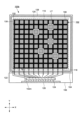
- FIGS. 13 and 14 illustrate images of the plurality of reflective elements 102 when the desired voltage is not applied to the liquid crystal layer 114.
- FIG. 13 and 14 illustrate images of the plurality of reflective elements 102 when the desired voltage is not applied to the liquid crystal layer 114.
- the first wiring 118 common to the column direction is shorted to a wiring such as the second wiring 132 to which a different potential is input than the first wiring 118.
- Brightness and Light Amount Voltages V0 to V4 are applied between the patch electrode 108 and the common electrode 110, respectively, and images of the multiple reflective elements 102 are captured.
- the absolute values of voltages V0 to V4 are set so that voltage V0 is the smallest and voltage V4 is the largest.
- the amount of light is less than the light LY around the patch electrode 108 of a normally operating reflective element 102, there is an insufficient voltage applied to the liquid crystal layer, and it is assumed that the electrical characteristic of the switching element connected to the patch electrode 108 is defective.
Landscapes
- Physics & Mathematics (AREA)
- Electromagnetism (AREA)
- Aerials With Secondary Devices (AREA)
- Liquid Crystal (AREA)
Abstract
電波反射装置の検査方法は、行方向および列方向に配列された複数の反射素子を有する電波反射装置の検査方法であって、複数の反射素子は、それぞれパッチ電極と、パッチ電極の背面側に重なるコモン電極と、複数のパッチ電極とコモン電極との間の液晶層と、を有し、電波反射板を構成する、電波反射装置の上方に位置する光源から第1偏光板を介して電波反射装置に第1光を照射し、電波反射装置の上方に位置する撮像装置は第1偏光板の透過軸と直交する透過軸を有する第2偏光板を介して電波反射板を画像に撮影し、画像において第1光の電波反射板で反射する第2光の有無に基づいて、反射素子の良否を判定する。
Description
本発明は、電波反射装置の検査方法に関する。
電波反射装置は、高層ビルの谷間など電波が届きにくい地帯(不感地帯)に電波を届けるために使用される。電波反射装置として、例えば、メインアレイ素子(ダイポール素子)及びサブアレイ素子(無給電素子)とコモン電極(接地電極)とが誘電体基板を挟んで設けられ、メインアレイ素子にサブアレイ素子が近接して配置された構成(特許文献1)、アレイ素子とコモン電極(接地電極)が誘電体基板を挟む構造において、コモン電極が周期的なループ形状を有する構成(特許文献2)が開示されている。
電波反射装置には誘電体基板が用いられるが、この誘電体基板に相当する部分を液晶層に置き換えると、液晶材料の誘電率異方性を利用することができ、反射波の指向性を可変にすることが可能となる。液晶材料を用いた電波反射装置は、反射素子がマトリクス状に配列された構成を有しており、パッチアレイが配列された平面アレイアンテナと同様の構成となっている。電波反射装置は、個々の反射素子を形成する液晶層の誘電率を電極間に印加する電圧によって変化させて、電波の反射方向を制御している。したがって、電波反射装置の良、不良を判断するには個々の反射素子の動作を検査する必要がある。しかしながら、液晶を用いる電波反射装置には、反射素子の良否を個々に検査していたのでは多大な時間を要し、生産性が低下するという問題があった。
このような問題に鑑み本発明の一実施形態は、電波反射装置の反射素子の良否を、全面を一度に観察して判定することができる検査方法を提供することを目的の一つとする。
本発明の一実施形態に係る電波反射装置の検査方法は、行方向および列方向に配列された複数の反射素子を有する電波反射装置の検査方法であって、複数の反射素子は、それぞれパッチ電極と、パッチ電極の背面側に重なるコモン電極と、複数のパッチ電極とコモン電極との間の液晶層と、を有し、電波反射板を構成する、電波反射装置の上方に位置する光源から第1偏光板を介して電波反射装置に第1光を照射し、電波反射装置の上方に位置する撮像装置は第1偏光板の透過軸と直交する透過軸を有する第2偏光板を介して電波反射板を画像に撮影し、画像において第1光の電波反射板で反射する第2光の有無に基づいて、反射素子の良否を判定する。
本発明の一実施形態に係る電波反射装置の検査方法は、行方向および列方向に配列された複数の反射素子を有する電波反射装置の検査方法であって、複数の反射素子は、それぞれパッチ電極と、パッチ電極の背面側に重なるコモン電極と、複数のパッチ電極とコモン電極との間の液晶層と、を有し、電波反射板を構成し、電波反射装置の上方に位置する光源から第3偏光板を介して電波反射装置に第1光を照射し、電波反射装置の上方に位置する撮像装置は第3偏光板を介して電波反射板120を画像に撮影し、画像における第1光の電波反射板120に反射した第3光の有無に基づいて、反射素子の良否を判定する。
以下、本発明の実施の形態を、図面などを参照しながら説明する。但し、本発明は多くの異なる態様で実施することが可能であり、以下に例示する実施の形態の記載内容に限定して解釈されるものではない。図面は説明をより明確にするため、実際の態様に比べ、各部の幅、厚さ、形状などについて模式的に表される場合があるが、あくまで一例であって、本発明の解釈を限定するものではない。また、本明細書と各図において、既出の図に関して前述したものと同様の要素には、同一の符号(又は数字の後にa、bなどを付した符号)を付して、詳細な説明を適宜省略することがある。さらに各要素に対する「第1」、「第2」と付記された文字は、各要素を区別するために用いられる便宜的な標識であり、特段の説明がない限りそれ以上の意味を有しない。
本明細書において、ある部材又は領域が他の部材又は領域の「上に(又は下に)」あるとする場合、特段の限定がない限りこれは他の部材又は領域の直上(又は直下)にある場合のみでなく他の部材又は領域の上方(又は下方)にある場合を含み、すなわち、他の部材又は領域の上方(又は下方)において間に別の構成要素が含まれている場合も含む。
1.反射素子
図1A及び図1Bは、本発明の一実施形態に係る電波反射装置100に用いられる反射素子102を示す。図1Aは、反射素子102を上方(電波が入射する側)からみたときの平面図を示し、図1Bは平面図に示すA1-A2間の断面図を示す。
図1A及び図1Bは、本発明の一実施形態に係る電波反射装置100に用いられる反射素子102を示す。図1Aは、反射素子102を上方(電波が入射する側)からみたときの平面図を示し、図1Bは平面図に示すA1-A2間の断面図を示す。
図1A及び図1Bに示すように、反射素子102は、誘電体基板104、対向基板106、パッチ電極108、コモン電極110、第1配向膜112a、第2配向膜112b、液晶層114を含む。反射素子102の中で誘電体基板104は一つの層をなすものとして誘電体層とみなすこともできる。パッチ電極108は誘電体基板104に設けられ、コモン電極110は対向基板106に設けられる。コモン電極110は、パッチ電極108の背面側に配置される。誘電体基板104にはパッチ電極108を覆うように第1配向膜112aが設けられ、対向基板106にはコモン電極110を覆うように第2配向膜112bが設けられる。パッチ電極108とコモン電極110とは対向するように配置され、両者の間に液晶層114が設けられる。パッチ電極108と液晶層114との間には第1配向膜112aが介在し、コモン電極110と液晶層114との間には第2配向膜112bが介在する。
パッチ電極108は、入射する電波の垂直偏波及び水平偏波に対して対称となる形状を有していることが好ましく、例えば平面視で正方形又は円形の形状を有する。ただし、あくまで好適な一例であって、当該形状に限定するものではない。図1Aは、パッチ電極108が平面視で正方形である場合を示す。コモン電極110の形状には特段の限定はなく、パッチ電極108よりも広い面積を有するように対向基板106の略全面に広がる形状を有する。パッチ電極108及びコモン電極110を形成する材料に限定はなく、導電性を有する金属、金属酸化物を用いて形成される。誘電体基板104には第1配線118が設けられていてもよい。第1配線118はパッチ電極108に接続される。第1配線118はパッチ電極108に制御信号を印加するときに用いることができる。また、第1配線118は、複数の反射素子が配列する場合、あるパッチ電極とそれに隣接するパッチ電極とを接続するときに用いることができる。
図1A及び図1Bには示されないが、誘電体基板104と対向基板106とは、シール材により貼り合わされる。誘電体基板104と対向基板106とは間隙を有するように対向配置され、液晶層114はシール材で囲まれる領域内に設けられる。液晶層114は誘電体基板104と対向基板106との間隙を充填するように設けられる。誘電体基板104と対向基板106との間隔は20~100μmであり、例えば、50μmの間隔を有する。誘電体基板104と対向基板106との間には、パッチ電極108、コモン電極110、第1配向膜112a、第2配向膜112bが設けられるため、正確には誘電体基板104と対向基板106の各々に設けられた第1配向膜112a及び第2配向膜112bの間の間隔が液晶層114の厚さとなる。なお、図1Bには図示されないが、誘電体基板104と対向基板106との間には間隔を一定に保つためのスペーサが設けられていてもよい。
パッチ電極108には液晶層114の液晶分子の配向を制御する制御信号が印加される。制御信号は直流電圧の信号、又は正の直流電圧と負の直流電圧が交互に反転する極性反転信号である。コモン電極110は接地又は極性反転信号の中間レベルの電圧が印加される。パッチ電極108に制御信号が印加されることで液晶層114に含まれる液晶分子の配向状態が変化する。液晶層114には誘電異方性を有する液晶材料が用いられる。例えば、液晶層114として、ネマチック液晶、スメクチック液晶、コレステリック液晶、ディスコティック液晶を用いることができる。誘電異方性を有する液晶層114は、液晶分子の配向状態の変化により誘電率が変化する。反射素子102は、パッチ電極108に印加する制御信号によって液晶層114の誘電率を変化させることができ、それによって電波を反射するときに反射波の位相を遅延させることができる。
反射素子102が反射する電波の周波数帯は、超短波(VHF:Very High Frequency)帯、極超短波(UHF:Ultra-High Frequency)帯、マイクロ波(SHF:Super High Frequency)帯、サブミリ波(THF:Tremendously high frequency)、ミリ波(EHF:Extra High Frequency)帯である。液晶層114の液晶分子はパッチ電極108に印加される制御信号に応答して液晶分子の配向が変化するが、パッチ電極108に照射される電波の周波数にはほとんど追従しない。したがって、反射素子102は、電波の影響を受けずに反射する電波の位相を制御することができる。
図2Aは、パッチ電極108とコモン電極110との間に電圧が印加されない状態(「第1の状態」とする)を示す。図2Aは、第1配向膜112a及び第2配向膜112bが水平配向膜である場合を示す。第1の状態における液晶分子116の長軸は、第1配向膜112a及び第2配向膜112bによりパッチ電極108及びコモン電極110の表面に対して水平に配向している。図2Bは、パッチ電極108に制御信号(電圧信号)が印加された状態(「第2の状態」とする)を示す。第2の状態において、液晶分子116は電界の作用を受けて長軸がパッチ電極108及びコモン電極110の表面に対し垂直に配向する。液晶分子116の長軸が配向する角度は、パッチ電極108に印加する制御信号の大きさ(コモン電極とパッチ電極間の電圧Vnの大きさ)によって、水平方向と垂直方向の中間の方向に配向させることもできる。
液晶分子116が正の誘電異方性を有する場合、第1の状態に対して第2の状態の方が、誘電率が大きくなる。また、液晶分子116が負の誘電異方性を有する場合も、予め垂直配向している場合は第1の状態に対して第2の状態の方が見かけ上の誘電率が高くなり、液晶分子116が水平配向している場合は見かけ上の誘電率がすでに高いため、電界をかけても水平配向から大きく配向が変化しない。誘電異方性を有する液晶層114は、可変誘電体層とみなすこともできる。反射素子102は、液晶層114の誘電異方性を利用して、反射波の位相を遅らせる(又は遅らせない)ように制御することができる。
反射素子102は、電波を所定の方向に反射する電波反射板に用いられる。反射素子102は、反射した電波の振幅がなるべく減衰しないことが好ましい。図1Bに示す構造から明らかなように、空中を伝搬する電波が反射素子102で反射されるとき電波は誘電体基板104を2回通過する。誘電体基板104は、例えば、ガラス、樹脂などの誘電体材料で形成される。
2.電波反射装置
次に、反射素子が集積された電波反射装置の構成を示す。
次に、反射素子が集積された電波反射装置の構成を示す。
2-1.電波反射装置A(一軸反射制御)
図3は、本発明の一実施形態に係る電波反射装置100aの構成を示す。電波反射装置100は電波反射板120を有する。電波反射板120は複数の反射素子102により構成される。複数の反射素子102は、例えば、列方向(図3に示すX軸方向)及び列方向に交差する列方向(図3に示すY軸方向)に配列される。反射素子102は、パッチ電極108が電波の入射面に向くように配置される。電波反射板120は平板状であり、この平板状の面内に複数のパッチ電極108がマトリクス状に配列される。
図3は、本発明の一実施形態に係る電波反射装置100aの構成を示す。電波反射装置100は電波反射板120を有する。電波反射板120は複数の反射素子102により構成される。複数の反射素子102は、例えば、列方向(図3に示すX軸方向)及び列方向に交差する列方向(図3に示すY軸方向)に配列される。反射素子102は、パッチ電極108が電波の入射面に向くように配置される。電波反射板120は平板状であり、この平板状の面内に複数のパッチ電極108がマトリクス状に配列される。
電波反射装置100aは、一つの誘電体基板104に複数の反射素子102が集積化された構造を有する。図3に示すように、電波反射装置100は、複数のパッチ電極108が配列された誘電体基板104と、コモン電極110が設けられた対向基板106とが重ねて配置され、2つの基板間に液晶層(図示されず)が設けられた構造を有する。電波反射板120は、複数のパッチ電極108とコモン電極110とが重畳する領域に形成される。電波反射板120の断面構造は、個々のパッチ電極108について見れば、図1Bに示す反射素子102の構造と同じである。誘電体基板104と対向基板106とはシール材128で貼り合わされており、図示されない液晶層はシール材128の内側の領域に設けられる。
誘電体基板104は対向基板106と対向する領域に加え、対向基板106より外側に広がる周辺領域122を有する。周辺領域122には第1駆動回路124及び端子部126が設けられる。第1駆動回路124はパッチ電極108に制御信号を出力する。端子部126は外部回路との接続を形成する領域であり、例えば、図示されないフレキシブルプリント回路基板(FPC)が接続される。端子部126には第1駆動回路124を制御する信号が入力される。
上記のように、誘電体基板104には複数のパッチ電極108が列方向(X軸方向)及び列方向(Y軸方向)に配列される。また、誘電体基板104には列方向(Y軸方向)に伸びる複数の第1配線118が配設される。複数の第1配線118のそれぞれは、列方向(Y軸方向)に配列する複数のパッチ電極108と電気的に接続される。別言すれば、列方向(Y軸方向)に配列する複数のパッチ電極108は第1配線118により連結される。電波反射板120は、第1配線118によって連結された一列のパッチ電極アレイが列方向(X軸方向)に複数個配列された構成を有する。
電波反射板120に配設された複数の第1配線118は周辺領域122に伸びて第1駆動回路124と接続される。第1駆動回路124は、複数の第1配線118のそれぞれに異なる電圧レベルの制御信号を出力することが可能である。これにより、電波反射板120では、列方向(X軸方向)及び列方向(Y軸方向)に配列された複数のパッチ電極108に対し、列ごと(列方向(Y軸方向)に配列されたパッチ電極108ごと)に制御信号が印加される。
電波反射装置100aは列方向(Y軸方向)に配列された複数のパッチ電極108の組ごとに制御信号が印加され、それにより電波反射板120に入射した電波の反射波の反射方向を制御することができる。すなわち、電波反射装置100aは、電波反射板120に照射された電波を、列方向(Y軸方向)に平行な反射軸VRを中心として図面の左右方向に反射波の進行方向を制御することができる。
図4は、2つの反射素子102によって反射波の進行方向が変化することを模式的に示す。反射素子102aと反射素子102bに同じ位相で電波が入射した場合において、反射素子102aと反射素子102bに異なる制御信号(V1≠V2)が印加されているために、反射素子102aに比べ反射素子102bによる反射波の位相変化が大きい場合を示す。その結果、反射素子102aで反射した反射波R1の位相と、反射素子102bで反射した反射波R2の位相が異なり(図4では反射波R2の位相が反射波R1の位相より進んでいる)、見かけ上、反射波の進行方向が斜め方向に変化する。
このような原理を図3に示す電波反射装置100aに適用し、例えば、反射素子による位相変化量の制御を列ごとに制御することにより、反射方向を一軸方向に制御することができる。
2-2.電波反射装置B(二軸反射制御)
図3に示す電波反射装置100aは反射軸VRが一軸であるため、反射軸VRを回転軸とした方向に反射角を制御することができる。これに対し本実施形態は、二軸反射制御をすることができる電波反射装置100bの一例を示す。以下の説明においては電波反射装置100aと異なる部分を中心に説明を行う。
図3に示す電波反射装置100aは反射軸VRが一軸であるため、反射軸VRを回転軸とした方向に反射角を制御することができる。これに対し本実施形態は、二軸反射制御をすることができる電波反射装置100bの一例を示す。以下の説明においては電波反射装置100aと異なる部分を中心に説明を行う。
電波反射装置100bは、行方向(X軸方向)に延伸する複数の第2配線132を有する。複数の第1配線118と複数の第2配線132は図示されない絶縁層を挟んで交差するように配置される。複数の第1配線118は第1駆動回路124に接続され、複数の第2配線132は第2駆動回路130に接続される。第2駆動回路130は走査信号を出力する。
図5Bは、4つのパッチ電極108と、2つの第1配線118及び第2配線132の配置102mを拡大した図を示す。4つのパッチ電極108のそれぞれにはスイッチング素子134が設けられる。スイッチング素子134のスイッチング(オン及びオフ)は第2配線132に印加される走査信号により制御される。スイッチング素子134がオンになったパッチ電極108は、第1配線118と導通し制御信号が印加される。スイッチング素子134は、例えば、薄膜トランジスタで形成される。このような構成によれば、行方向(X軸方向)に配列する複数のパッチ電極108を行ごとに選択し、各行に異なる電圧レベルの制御信号を印加することができる。
図5Aに示す電波反射装置100bは、電波反射板120に照射された電波を、列方向(Y軸方向)に平行な反射軸VRを中心として図面の左右方向に反射波の進行方向を制御することができることに加え、列方向(X軸方向)に平行な反射軸HRを中心として図面の上下方向へも反射波の進行方向を制御することができる。すなわち、電波反射装置100bは、列方向(Y軸方向)に平行な反射軸VRと、列方向(X軸方向)に平行な反射軸HRを有するため、反射軸VRを回転軸とした方向、反射軸HRを回転軸とした方向に反射角を制御することができる。
このような原理を図5Aに示す電波反射装置100bに適用し、例えば、反射素子による位相変化量の制御を列、行ともに独立して制御することにより、反射方向を一軸方向および二軸方向に制御することができる。
図6は、パッチ電極108にスイッチング素子134が接続された反射素子102の断面構造の一例を示す。スイッチング素子134が誘電体基板104に設けられる。スイッチング素子134はトランジスタであり、第1ゲート電極138、第1ゲート絶縁層140、半導体層142、第2ゲート絶縁層146、第2ゲート電極148が積層された構造を有する。第1ゲート電極138と誘電体基板104との間にはアンダーコート層136が設けられていてもよい。第1ゲート絶縁層140と第2ゲート絶縁層146との間に第1配線118が設けられる。第1配線118は半導体層142と接するように設けられる。また、第1配線118を形成する導電層と同じ層で第1接続配線144が設けられる。第1接続配線144は半導体層142と接するように設けられる。第1配線118及び第1接続配線144の半導体層142に対する接続構造は、一方の配線がトランジスタのソースに接続され、もう一方の配線がドレインに接続された構造を示す。
スイッチング素子134を覆うように第1層間絶縁層150が設けられる。第1層間絶縁層150の上に第2配線132が設けられる。第2配線132は、第1層間絶縁層150に形成されたコンタクトホールを介して第2ゲート電極148と接続される。なお、図示されないが、第1ゲート電極138と第2ゲート電極148とは半導体層142と重ならない領域で相互に電気的に接続されている。第1層間絶縁層150の上には、第2配線132と同じ導電層で第2接続配線152が設けられる。第2接続配線152は、第1層間絶縁層150に形成されたコンタクトホールを介して第1接続配線144と接続される。
第2配線132及び第2接続配線152を覆うように第2層間絶縁層154が設けられる。さらにスイッチング素子134の段差を埋めるように平坦化層156が設けられる。平坦化層156を設けることにより、スイッチング素子134の配置に影響を受けずにパッチ電極108を形成することができる。平坦化層156の平坦な表面の上にパッシベーション層158が設けられる。パッチ電極108はパッシベーション層158の上に設けられる。パッチ電極108は、パッシベーション層158、平坦化層156、及び第2層間絶縁層154を貫通するコンタクトホールを介して第2接続配線152と接続される。パッチ電極108の上に第1配向膜112aが設けられる。
対向基板106は、図1Bと同様に、コモン電極110、第2配向膜112bが設けられる。誘電体基板104のスイッチング素子134及びパッチ電極108が設けられた面が対向基板のコモン電極110が設けられた面が対向するように配置され、その間に液晶層114が設けられる。誘電体基板104の厚さTは、パッチ電極108の液晶層114側の表面から誘電体基板104のパッチ電極108が設けられる面とは反対側の面までの長さとすることができる。この場合、パッチ電極108と誘電体基板104との間にある少なくとも1層の絶縁層(アンダーコート層136、第1ゲート絶縁層140、第2ゲート絶縁層146、第1層間絶縁層150、第2層間絶縁層154、平坦化層156、パッシベーション層158)の厚さを考慮に入れることができる。
誘電体基板104に形成される各層は以下のような材料を用いて形成される。アンダーコート層136は、例えば、シリコン酸化膜で形成される。第1ゲート絶縁層140、第2ゲート絶縁層146は、例えば、酸化シリコン膜、又は酸化シリコン膜と窒化シリコン膜の積層構造で形成される。半導体層は、アモルファスシリコン、多結晶シリコンのようなシリコン半導体、酸化インジウム、酸化亜鉛、酸化ガリウムなどの金属酸化物を含む酸化物半導体で形成される。第1ゲート電極138及び第2ゲート電極148は、例えば、モリブデン(Mo)、タングステン(W)又はこれらの合金で構成されてもよい。第1配線118、第2配線132、第1接続配線144、及び第2接続配線152は、チタン(Ti)、アルミニウム(Al)、モリブデン(Mo)などの金属材料を用いて形成される。例えば、チタン(Ti)/アルミニウム(Al)/チタン(Ti)の積層構造、又はモリブデン(Mo)/アルミニウム(Al)/モリブデン(Mo)の積層構造で構成されてもよい。平坦化層156は、アクリル、ポリイミドなどの樹脂材料で形成される。パッシベーション層158は、例えば、窒化シリコン膜などで形成される。パッチ電極108及びコモン電極110は、アルミニウム(Al)、銅(Cu)などの金属膜で形成される。
図6に示すように、第2配線132をスイッチング素子134として用いるトランジスタのゲートに接続し、第1配線118を当該トランジスタのソース及びドレインの一方に接続し、パッチ電極108をソース及びドレインの他方に接続することで、マトリクス状に配列された複数のパッチ電極108の中から所定のパッチ電極を選択して制御信号を印加することができる。そして、電波反射板120の中の個々のパッチ電極108にスイッチング素子134を設けることにより、第1方向(X軸方向)に沿って横一列に配列されるパッチ電極108ごと、又は第2方向(Y軸方向)に沿って縦一列に配列されるパッチ電極108ごとに制御電圧を印加することができ、例えば、電波反射板120が直立しているとき、左右方向及び上下方向に反射波の反射方向を制御することができる。
3.検査装置
次に、図7および図8を参照し、電波反射装置100の検査に用いられる検査装置200を説明する。
次に、図7および図8を参照し、電波反射装置100の検査に用いられる検査装置200を説明する。
検査装置200は、基本的な構成として、光源202、撮像装置204、試料台206、および偏光板208を有する。図7は、本発明の一実施形態に係る電波反射装置の検査に用いる検査装置の断面図である。
光源202は、例えば、白色光を電波反射装置100の全面(電波反射板120の全面)に光を照射することのできる照射エリアを有する。光源202は、試料台206の斜め上方に配置される。撮像装置204は、光源202から出射された光が直接入射しないように配置される。光源202は、試料台206の上に電波反射装置100が設置された場合、光源202から照射された光が、電波反射装置100の電波反射板120の全体を照射するように配置される。詳細は後述するが、このとき、電波反射装置100は、パッチ電極108が配列された電波反射板120に、光源202から出射された光が入射されるように、試料台206の上に設置される。パッチ電極108は金属で形成されているため、光源202は、電波反射装置100を試料台206の上に配置したときに、電波反射板120の中に光源202が映り込まないように斜め上方に配置される。光源202は、例えば、ハロゲンランプの光をライトガイドで導いた面照射型の発光源、又は白色LEDや蛍光ランプを用いた面光源を用いることができる。
撮像装置204は、光源202から偏光板208を介して出射され、電波反射板120で反射された光LYを、偏光板208を介して撮像する。撮像装置204は、試料台206の上方に位置し、電波反射板120で反射した光が入射する位置に配置される。撮像装置204は、試料台206の上に電波反射装置100が設置された場合、電波反射板120の全面を1枚の画像として取得できる視野角を有する。撮像装置204には、例えば、デジタルカメラやビデオカメラなどのカメラを用いることができる。撮像装置204が、パッチ電極108が配列された電波反射板120の全面を1枚の画像で撮影することにより、電波反射装置100全体の観察にかかる時間を短縮することができる。
上述にて撮像装置204について言及したが、光源202から偏光板208を介して出射され、電波反射板120で反射された光LYの像を実際に目視にて確認しても良い。
試料台206は、電波反射装置100を安定に保持することができるように平坦な面を有する。試料台206には、電波反射装置100を固定する固定部材や真空チャックなどが備えられていてもよい。
偏光板208は直線偏光板であり、光源202から出射された光のうち一方向の偏光成分の光を透過する。したがって、電波反射装置100には、直線偏光の光が照らされる。偏光板208は、光源202側と撮像装置204側に配置される。具体的に、図7に示すように、偏光板208-1は、電波反射装置100と光源202との間に配置され、偏光板208-2は、撮像装置204との間に配置される。偏光板208-1と偏光板208-2とは、透過軸が直交するように配置(クロスニコル)される。図7に示すように、偏光板208-1の透過軸TA1と偏光板208-2の透過軸TA2は、直交する。電波反射装置100の液晶分子116が図2Aに示される第1の状態で配向している方向と偏光板208-1を介して出射された偏光方向とが並行又は垂直とする。偏光板208-1と偏光板208-2は、向き合って配置されず、それぞれ電波反射装置100または試料台206の方を向くように配置される。
このような2枚の偏光板の組み合わせにより、光源202から偏光板208-1を介して出射された光(直線偏光成分LX)に対し、電波反射装置100で反射された光のうち、偏光方向が90°回転した光(直線偏光成分LY)が偏光板208-2を透過して撮像装置204に入射する。すなわち、撮像装置204は、光源202から出射した光をそのまま受光して撮像するのではなく、液晶層114によって直線偏光成分LXの偏光状態が維持されなかった直線偏光成分LYの光を受光して撮像を行う。液晶層114が直線偏光成分LXの偏光状態を維持するか否かは、パッチ電極108とコモン電極110の間のバイアス状態に依存する。本実施形態の検査装置200は、液晶層114のこのような特性を利用して、電波反射板120を形成する反射素子102の良否(正常に動作する良品であるか、動作しない不良品であるか)を検査する。
図7は、検査装置200が、2枚の直線偏光板で構成される例を示すが、偏光板の構成はこの例に限定されない。偏光板208に、直線偏光板と1/4波長板を組み合わせた偏光板、例えば、円偏光板を用いる場合、1枚の偏光板で検査装置200を構成することができる。例えば、図8に示すように、円偏光板を用いる場合には、光源202および撮像装置204との間にそれぞれ偏光板208を配置せず、光源202および撮像装置204との間に偏光板208C(円偏光板)を配置すればよい。
偏光板208Cは、光源202から出射する光LVを偏光にし、偏光の電波反射装置100で正反射した光を除去し、その他の光を透過(光LW)させることができる。偏光板208Cは、電波反射装置100または電波反射板120を覆うことができる大きさであるとよい。
4.検査方法
次に、図7を再度参照し、電波反射装置100の検査方法を説明する。
次に、図7を再度参照し、電波反射装置100の検査方法を説明する。
はじめに、パッチ電極108を観察できる方向を上面として、上面から観察できるように、電波反射装置100を検査装置200に設置する。例えば、図7に示すように、検査装置の試料台206の上に反射素子102のパッチ電極108が光源202および撮像装置204側に、コモン電極110が試料台206側になるように、電波反射装置100を設置する。
次に、パッチ電極108とコモン電極110との間に電圧V0から電圧V2を印加し、光源202から偏光板208-1を介して電波反射装置100に光を照射する。本実施形態において、電圧V0はパッチ電極108とコモン電極110間の電圧が0Vであることを示し、0Vの印加も電圧の印加に含まれる。また、電圧V0から電圧V2は互いに異なる電圧である。さらに、それぞれの電圧V0から電圧V2の絶対値は、電圧V0、電圧V1、電圧V2の順に大きい。これら印加電圧は、電圧V0からV2に限らず、反射素子102が低位相差から高位相差まで設定できる範囲で適宜設定することができる。
パッチ電極108とコモン電極110との間に電圧を印加すること、電波反射装置100に光を照射することは、上述したような順序である必要はない。例えば、パッチ電極108とコモン電極110との間に電圧を印加する前に、電波反射装置100に光を照射してもよい。
さらに、各々の電圧印加時には、撮像装置204を用いて、電波反射板120の全面が1枚の画像に収まるように撮影する。このとき、電波反射板120は偏光板208-2を介して撮影される。
最後に、反射素子102の良否判定は、撮像装置204で撮影した画像において光(直線偏光成分LX)の反射素子102で反射した光(直線偏光成分LY)の有無、および光(直線偏光成分LY)の明るさまたは光量に基づいて行われる。光(直線偏光成分LY)の有無および明るさまたは光量については、後述する。
<判定基準>
はじめに、図9Aから図9Cを参照し、パッチ電極108とコモン電極110との間に印加された電圧に対応する所望の電圧が液晶層に印加された反射素子102について説明をする。図9Aから図9Cは、本発明の一実施形態に係る電波反射装置に用いられる反射素子の平面図を示す。
はじめに、図9Aから図9Cを参照し、パッチ電極108とコモン電極110との間に印加された電圧に対応する所望の電圧が液晶層に印加された反射素子102について説明をする。図9Aから図9Cは、本発明の一実施形態に係る電波反射装置に用いられる反射素子の平面図を示す。
パッチ電極108およびコモン電極110との間に電圧V0を印加、または、反射素子102のパッチ電極108およびコモン電極110との間の電圧を未印加とする。このとき、反射素子102を上面から観察すると、図9Aに示す反射素子102aおよび反射素子102bのように、パッチ電極108の外周に枠状領域160は現れない。
パッチ電極108およびコモン電極110との間に電圧V1を印加する。このとき、反射素子102を上面から観察すると、図9Bに示すように、パッチ電極108の外周に枠状領域160が現れる。枠状領域160は、上面視においてパッチ電極108を囲む。
パッチ電極108およびコモン電極110との間に電圧V2を印加する。このとき、反射素子102を上面から観察すると、図9Cに示すように、パッチ電極108の外周に枠状領域160が現れる。図9Cに示す枠状領域160の幅は、電圧V2の絶対値が電圧V1の絶対値より大きい関係と同様に、図9Bに示す枠状領域160の幅より大きい。また、電圧V2の絶対値が電圧V1の絶対値より大きいことにより、反射素子102は電圧V1がパッチ電極108およびコモン電極110との間に印加された反射素子102に設定される位相変化量より高い位相変化量を設定することができる。
次に、図10を参照し、光源202から偏光板208-1を介して光が反射素子102に照射され、反射素子102で反射した光について説明する。図10は、本発明の一実施形態に係る電波反射装置における反射素子の断面図を示す。
光源202から出射された光は、その光のうちの直線偏光成分LX0の光が偏光板208-1を通過し、光LX0は反射素子102に照射される。照射された直線偏光成分LX0の光は、パッチ電極108に正反射する。パッチ電極108で反射した光は、光LX0の偏光が維持された状態であり、直線偏光成分LX1である。
直線偏光成分LX0の光は、パッチ電極108の他に、コモン電極110にも照射され、正反射する。このとき、直線偏光成分LX0の光は、上面視において隣接するパッチ電極108の間を通り、コモン電極110に反射する。例えば、図10に示すように、隣接する反射素子102aのパッチ電極108と反射素子102bのパッチ電極108との間から液晶層114を通り、コモン電極110に反射する。図9Aに示す反射素子102には、パッチ電極108とコモン電極110との間に電圧V0が印加(電圧が印加されない状態)されているため、コモン電極110に反射した光は、光LX0の偏光が維持された状態であり、直線偏光成分LX2である。
直線偏光成分LX1および直線偏光成分LX2の光は、上述したように、偏光板208-2が偏光板208-1にクロスニコルとなるように配置されているため、偏光板208-2によって遮蔽され、撮像装置204に到達しない。直線偏光成分LX1およびLX2の光は、撮像装置204に到達しないことにより、撮像装置204に検出されず、複数の反射素子102の画像に映らない。
したがって、電波反射板120におけるそれぞれのパッチ電極108とコモン電極110の間に電圧V0を印加し、電波反射板120の画像において、反射素子102に反射した光が存在しなければ、液晶層114に正常に電圧がかかっていると判定することができる。
次に、図11を参照し、光源202から偏光板208-1を介して反射素子102に光が照射され、反射素子102で反射した光について説明する。図11は、図9Bに示す反射素子102の断面図を示す。
図11に示すように、枠状領域160は、液晶層114の一部の上面である。枠状領域160を上面とする液晶層114の一部は、パッチ電極108とコモン電極110との間に電圧V1が印加されたときに、パッチ電極108とコモン電極110との間に形成される斜め電界(上下矢印)により配向した液晶である。上下矢印で示した斜め電界は、例示であって制限的なものではない。
詳細には、枠状領域160を上面とする液晶層114の一部は、パッチ電極108の端部またはその周辺とコモン電極110との間に形成される斜め電界の漏れ出しによる液晶の配向を示す。斜め電界の漏れ出しとは、図11に示すように、パッチ電極108とコモン電極110との間をパッチ電極108の幅108w内の電界に対し、幅108wより外側に形成されている電界を指し示す。したがって、図9Bに示すように、上面視からそれらの電界による液晶の配向をパッチ電極108の外周に現れる枠状領域160として視認可能であり、パッチ電極108とコモン電極110との間にかけられる電圧によって変化する。
また、図9Bに示すように、幅108wより外側に形成されている電界によって配向する液晶層の一部は、パッチ電極108とコモン電極110との間をパッチ電極108の幅108w内の電界によって配向する液晶層114を挟むように位置する。
光源202から偏光板208-1を介して照射される直線偏光成分LX0の光は、上述したようにパッチ電極108とコモン電極110に反射する。パッチ電極108に反射した光は上述したように光LX0の偏光が維持された状態である直線偏光成分LX1であり、コモン電極110に反射した光は、直線偏光成分LX0の偏光が維持された状態の直線偏光成分LX2の光と偏光が維持されていない状態の光LY2が含まれる。
光LY2は、直線偏光成分LX0の光が配向した一部の液晶層114を通りコモン電極110に反射、または、コモン電極110に反射し配向した一部の液晶層114を通ることにより、直線偏光成分LX0の偏光が維持されない状態となる。直線偏光成分LX0の偏光が維持されない状態とは、例えば、光LY2が、直線偏光成分LX0の光が配向した一部の液晶層114を通ることにより、楕円偏光または非偏光である散乱光等となる場合である。
光LY2は、上述したように直線偏光成分LX0の偏光が維持されない状態ではないため、偏光板208-2によって遮蔽されず、撮像装置204に到達することができる。光LY2は、撮像装置204により検出され、電波反射板120の画像に映る。電波反射板120の画像に映る光LY2は、詳細は後述するが、上面視においてパッチ電極108の周りを囲む光として映ることができる。
したがって、電波反射板120においてそれぞれのパッチ電極108とコモン電極110の間に電圧V1を印加し、直線偏光成分LX2の光が電波反射板120の画像に一様な明るさまたは光量で映るとき、液晶層114に正常に電圧がかかっていると判定することができる。
次に、図12を参照し、光源202から偏光板208-1を介して光を照射されたときの図9Cに示す反射素子102の断面構造について説明する。図12は、図9Cに示す反射素子102の断面図を示す。図11に示す反射素子102と異なる点は、パッチ電極108とコモン電極110との間に印加される電圧の絶対値が電圧V1の絶対値より大きい点である。なお、図11に示す反射素子102と同一、または、類似する構成については、説明を割愛することがある。
図12に示すように、枠状領域160は、液晶層114の一部の上面である。枠状領域160を上面とする液晶層114の一部は、パッチ電極108とコモン電極110との間に電圧V2が印加されたときに、パッチ電極108とコモン電極110との間に形成される斜め電界(上下矢印)により配向した液晶である。上下矢印で示した斜め電界は、例示であって制限的なものではない。
パッチ電極108とコモン電極110との間に電圧V2を印加したときに形成される電界は、パッチ電極108とコモン電極110との間に電圧V1を印加したときに比べより強く、図9Bおよび図9Cに示したように、パッチ電極108の外周に現れる枠状領域160の幅は大きくなり、図11および図12においても、電界の広がりが大きくなる。
光源202から偏光板208-1を介して照射される直線偏光成分LX0の光は、上述したようにパッチ電極108とコモン電極110に反射する。パッチ電極108に反射した直線偏光成分LX1の光は上述したように直線偏光成分LX0の偏光が維持された状態にあり、コモン電極110に反射した光は、直線偏光成分LX0の偏光が維持された状態の直線偏光成分LX2と偏光が維持されない状態の光LY3が含まれる。
光LY3は、光LX0が配向した一部の液晶層114を通りコモン電極110に反射する、または、コモン電極110に反射し配向した一部の液晶層114を通ることにより、直線偏光成分LX0の偏光が維持されない状態となる。光LY3は、パッチ電極108とコモン電極110との間に電圧V1を印加したときに比べ枠状領域160の幅は大きいことにより、枠状領域160を通る直線偏光成分LX0の光が増え、光LY2より直線偏光成分LX0の偏光が維持されていない状態の光の量が増える。
光LY3は、上述したように直線偏光成分LX0の偏光が維持された状態ではないため、偏光板208-2によって遮蔽されず、撮像装置204に到達することができる。光LY3は、撮像装置204に検出され、電波反射板120の画像に映る。電波反射板120の画像に映る光LY3は、上述した光LY2と同様に、上面視においてパッチ電極108の周りを囲む光として映ることができる。ただし、電波反射板120の画像に映る光LY3の明るさまたは光量は、電波反射板120の画像に映る光LY2の明るさおよび光量と異なる。例えば、電圧V2で絶対値が電圧V1の絶対値より大きい場合、電波反射板120の画像において、光LY3の明るさは、光LY2の明るさより明るい。
したがって、電波反射板120においてそれぞれのパッチ電極108とコモン電極110の間に電圧V2を印加したとき、正常に駆動する反射素子102を有する複数の反射素子102の画像には、光LX3が一様な明るさまたは光量で映る。光LX3の光量は光LX2の光量より大きく、複数の反射素子102の画像において、光LX3は光LX2より明るく映り、液晶層114に正常に電圧がかかっていると判定することができる。
パッチ電極108とコモン電極110の間に印加する電圧は、上述したような電圧V0からV2までに限定されず、例えば、電圧V0の絶対値より大きく、電圧V1の絶対値より小さい電圧や、電圧V1の絶対値より大きく、電圧V2の絶対値より小さい電圧等を印加してもよい。
パッチ電極108とコモン電極110の間には、隣接する反射素子102間で異なる電圧を印加してもよい。例えば、図10に示す反射素子102aのパッチ電極108とコモン電極110の間には電圧V1を印加し、反射素子102bのパッチ電極108とコモン電極110の間には電圧V2を印加してもよい。このとき、撮像装置によって、反射素子102bのパッチ電極108の周囲に直線偏光成分LX3の光が検出され、反射素子102aパッチ電極108の周囲に直線偏光成分LX2の光が検出され、電波反射板120の画像に上述した直線偏光成分LX2および直線偏光成分LX3の光が映る場合、各反射素子102の液晶層114に正常に電圧がかかっていると判定することができる。
パッチ電極108とコモン電極110の間には、各列の反射素子102間で異なる電圧を印加してもよい。例えば、図3に示す列方向に配列される複数の反射素子102において、第1配線118aに接続するパッチ電極108とコモン電極110の間に電圧V1を印加し、第1配線118bに接続するパッチ電極108とコモン電極110の間に電圧V2を印加してもよい。このとき、撮像装置204によって、第1配線118aに接続するパッチ電極108の周囲に光が一様な明るさで検出され、第1配線118bに接続するパッチ電極108の周囲に光が一様で第1配線118aに接続するパッチ電極108の周囲の光より明るい明るさで検出され、電波反射板120の画像に上述した直線偏光成分LX2の光および直線偏光成分LX3の光が映る場合、各反射素子102の液晶層114に正常に電圧がかかっていると判定することができる。
以上のように、本発明の一実施形態に係る電波反射装置100の検査方法は、電波反射装置100の複数の反射素子102のそれぞれのパッチ電極108とコモン電極110の間に所望の電圧を印加し、光源202から偏光板208-1を介して電波反射装置100に直線偏光成分LX0の光を照射し、撮像装置204は偏光板208-2を介して電波反射板120を画像に撮影する。その画像において、上述した電圧に対応した、コモン電極110に反射した光の有無、あるいは、明るさ、光量に基づいて、それぞれの反射素子102の良否を判定することができる。このような良否判定は、電波反射装置100の電波反射板120の全面を一度に観察して判定することが可能となり、反射素子の良否の判定の時間を短くすることができる。
5.不良モード
5-1.画像
図13および図14は、所望の電圧が液晶層114に印加されなかった場合の複数の反射素子102の画像を例示する。
5-1.画像
図13および図14は、所望の電圧が液晶層114に印加されなかった場合の複数の反射素子102の画像を例示する。
電波反射板120の全てのパッチ電極108とコモン電極110との間に電圧V0を印加し、正常に駆動しない反射素子102があった。図13には、パッチ電極108とコモン電極110との間に電圧V0が印加されたところ、2列にわたる複数の反射素子102に異常電圧が印加されている。異常電圧が印加された反射素子102のパッチ電極108の周囲は、コモン電極110に反射した直線偏光成分LX0の偏光状態が維持されなかった状態の光LYが検出され、画像に光LYが映されている。
上述した不良モードの場合、例えば、列方向に共通する第1配線118が第2配線132などの第1配線118と異なる電位が入力されている配線とショートしていることが想定される。
図14には、パッチ電極108とコモン電極110との間に電圧V0が印加されたところ、一列に配列していない複数の反射素子102のパッチ電極108とコモン電極110間に異常電圧が印加されている。異常電圧が印加されたパッチ電極108の周囲は、直線偏光成分LX0の偏光状態が維持されなかった状態のコモン電極110に反射した異常の光LYが検出され、画像に光LYが映されている。
上述した不良モードの場合、光LYが囲むパッチ電極108が電気的に接続するスイッチング素子134の不良であることが想定される。さらに、上述した不良モードの場合、パッチ電極108とコモン電極110との間に電圧V0が印加されているにも関わらずパッチ電極108とコモン電極110間に電圧がかかっている状態であるため、パッチ電極108が第2配線132にショートしていることも想定される。
5-2.明るさおよび光量
パッチ電極108とコモン電極110間に電圧V0から電圧V4までそれぞれ印加し、複数の反射素子102の画像を撮像する。電圧V0から電圧V4までの絶対値は、電圧V0が最も小さく、逆に電圧V4が最も大きいものとする。各電圧で撮像された画像において、パッチ電極108の周囲で検出される光LYに関して、光LYの明るさまたは光量がパッチ電極108とコモン電極110間に印加される電圧に対応しているかどうかを確認する。光LYの明るさまたは光量がパッチ電極108とコモン電極110間に印加される電圧に対応していない場合、以下の不良モードAからDが想定される。
パッチ電極108とコモン電極110間に電圧V0から電圧V4までそれぞれ印加し、複数の反射素子102の画像を撮像する。電圧V0から電圧V4までの絶対値は、電圧V0が最も小さく、逆に電圧V4が最も大きいものとする。各電圧で撮像された画像において、パッチ電極108の周囲で検出される光LYに関して、光LYの明るさまたは光量がパッチ電極108とコモン電極110間に印加される電圧に対応しているかどうかを確認する。光LYの明るさまたは光量がパッチ電極108とコモン電極110間に印加される電圧に対応していない場合、以下の不良モードAからDが想定される。
不良モードAの反射素子102の例を説明する。パッチ電極108の周囲で検出される光LYは、それぞれ電圧V0から電圧V4までパッチ電極108とコモン電極110との間に印加すると、電圧V0から電圧V2までは印加した電圧に対応する明るさまたは光量の光がそれぞれ検出され、高電位である電圧V3から電圧V4では検出されない。不良モードAでは、パッチ電極108に接続するスイッチング素子134の電気特性に不良があることが想定される。
不良モードBの反射素子102の例を説明する。光LYは、それぞれ電圧V0から電圧V4までパッチ電極108とコモン電極110との間に印加すると、電圧V0から電圧V2までは検出されず、高電位である電圧V3から電圧V4では印加した電圧に対応する明るさまたは光量の光がそれぞれ検出される。これより、不良モードBでは、液晶層にかかる電圧が不足していることが分かる。電圧不足の原因は、パッチ電極108に接続するスイッチング素子134の電気特性に不良があることが想定される。また、正常に駆動している反射素子102のパッチ電極108の周囲の光LYに比べ光量が少ない場合、液晶層にかかる電圧の不足がみられ、パッチ電極108に接続するスイッチング素子の電気特性に不良があることが想定される。
不良モードCの反射素子102の例を説明する。光LYは、それぞれ電圧V0から電圧V4までパッチ電極108とコモン電極110との間に印加するが、変化が見られない。具体的には、光LYは、印加される電圧に関係なく検出されない。これより、不良モードCでは、パッチ電極108に接続するスイッチング素子のオープン不良、およびパッチ電極108とスイッチング素子間の接続不良等が想定される。
不良モードDの反射素子102の例を説明する。光LYは、それぞれ電圧V0から電圧V4までパッチ電極108とコモン電極110との間に印加するが、変化が見られない。具体的には、光LYは、印加される電圧に関係なく検出される。これより、不良モードDでは、スイッチング素子のソース-ドレイン間のショート、またはドレイン-ゲート間のショートが考えられ、ソースと接続する信号線またはゲート電極と接続するゲート線からの電圧が直接常に液晶層にかかってしまい、スイッチング素子のオン、オフに関係なく光LYが検出されてしまうことが想定される。
以上のように、印加される電圧による光LYの有無、または明るさおよび光量の変化を観察することによって、液晶層に所望の電圧がかからない反射素子102を不良モードに分類することができる。
本発明の実施形態として上述した各実施形態は、相互に矛盾しない限りにおいて、適宜組み合わせて実施することができる。また、各実施形態を基にして、当業者が適宜構成要素の追加、削除もしくは設計変更を行ったもの、又は、工程の追加、省略もしくは条件変更を行ったものも、本発明の要旨を備えている限り、本発明の範囲に含まれる。
上述した各実施形態の態様によりもたらされる作用効果とは異なる他の作用効果であっても、本明細書の記載から明らかなもの、または、当業者において容易に予測し得るものについては、当然に本発明によりもたらされるものと解される。
100:電波反射装置、100a:電波反射装置、100b:電波反射装置、102:反射素子、102a:反射素子、102b:反射素子、102m:配置、104:誘電体基板、106:対向基板、108:パッチ電極、108w:幅、110:コモン電極、112a:第1配向膜、112b:第2配向膜、114:液晶層、116:液晶分子、118:第1配線、118a:第1配線、118b:第1配線、120:電波反射板、122:周辺領域、124:第1駆動回路、126:端子部、128:シール材、130:第2駆動回路、132:第2配線、134:スイッチング素子、136:アンダーコート層、138:第1ゲート電極、140:第1ゲート絶縁層、142:半導体層、144:第1接続配線、146:第2ゲート絶縁層、148:第2ゲート電極、150:第1層間絶縁層、152:第2接続配線、154:第2層間絶縁層、156:平坦化層、158:パッシベーション層、160:枠状領域、200:検査装置、202:光源、204:撮像装置、206:試料台、208:偏光板、208-1:偏光板、208-2:偏光板、208C:偏光板
Claims (13)
- 行方向および列方向に配列された複数の反射素子を有する電波反射装置の検査方法であって、
前記複数の反射素子は、それぞれパッチ電極と、前記パッチ電極の背面側に重なるコモン電極と、前記複数のパッチ電極と前記コモン電極との間の液晶層と、を有し、電波反射板を構成し、
前記電波反射装置の上方に位置する光源から第1偏光板を介して前記電波反射装置に第1光を照射し、
前記電波反射装置の上方に位置する撮像装置は前記第1偏光板の透過軸と直交する透過軸を有する第2偏光板を介して前記電波反射板を画像に撮影し、
前記画像において前記第1光の前記電波反射板で反射する第2光の有無に基づいて、前記反射素子の良否を判定する、電波反射装置の検査方法。 - 前記複数のパッチ電極と前記コモン電極との間に電圧V0をそれぞれ印加し、
前記電圧V0は、前記複数のパッチ電極と前記コモン電極との間に電圧が印加されない状態である、請求項1に記載の電波反射装置の検査方法。 - 前記複数のパッチ電極と前記コモン電極との間に、前記電圧V0と異なる電圧V1をそれぞれ印加し、
前記画像において前記第2光の明るさに基づいて、前記反射素子の良否を判定する、
請求項2に記載の電波反射装置の検査方法。 - 前記複数のパッチ電極に電圧V1より電位の大きい電圧V2をそれぞれ印加し、
前記画像において前記第2光の明るさに基づいて、前記反射素子の良否を判定する、
請求項3に記載の電波反射装置の検査方法。 - 前記撮像装置は、前記電波反射板の全面を1枚の前記画像に撮影するように配置される、請求項1に記載の電波反射装置の検査方法。
- 前記光源は、面光源である、請求項1に記載の電波反射装置の検査方法。
- 行方向および列方向に配列された複数の反射素子を有する電波反射装置の検査方法であって、
前記複数の反射素子は、それぞれパッチ電極と、前記パッチ電極の背面側に重なるコモン電極と、前記複数のパッチ電極と前記コモン電極との間の液晶層と、を有し、電波反射板を構成し、
前記電波反射装置の上方に位置する光源から第3偏光板を介して前記電波反射装置に第1光を照射し、
前記電波反射装置の上方に位置する撮像装置は前記第3偏光板を介して前記電波反射板を画像に撮影し、
前記画像における第1光の前記電波反射板に反射した第3光の有無に基づいて、前記反射素子の良否を判定する、電波反射装置の検査方法。 - 前記複数のパッチ電極と前記コモン電極との間に電圧V0をそれぞれ印加し、
前記電圧V0は、前記複数のパッチ電極と前記コモン電極との間に電圧が印加されない状態である、請求項7に記載の電波反射装置の検査方法。 - 前記複数のパッチ電極と前記コモン電極との間に、前記電圧V0と異なる電圧V1をそれぞれ印加し、
前記画像において前記第3光の明るさに基づいて、前記反射素子の良否を判定する、
請求項8に記載の電波反射装置の検査方法。 - 前記複数のパッチ電極に電圧V1より電位の大きい電圧V2をそれぞれ印加し、
前記画像において前記第3光の明るさに基づいて、前記反射素子の良否を判定する、
請求項9に記載の電波反射装置の検査方法。 - 前記第3偏光板は、前記電波反射装置と前記光源および前記撮像装置との間に配置される、請求項7に記載の電波反射装置の検査方法。
- 前記撮像装置は、前記電波反射板の全面を1枚の前記画像に撮影するように配置される、請求項7に記載の電波反射装置の検査方法。
- 前記光源は、面光源である、請求項7に記載の電波反射装置の検査方法。
Priority Applications (2)
| Application Number | Priority Date | Filing Date | Title |
|---|---|---|---|
| CN202480039052.1A CN121312019A (zh) | 2023-07-14 | 2024-05-22 | 电波反射装置的检查方法 |
| JP2025533887A JPWO2025018024A1 (ja) | 2023-07-14 | 2024-05-22 |
Applications Claiming Priority (2)
| Application Number | Priority Date | Filing Date | Title |
|---|---|---|---|
| JP2023-116266 | 2023-07-14 | ||
| JP2023116266 | 2023-07-14 |
Publications (1)
| Publication Number | Publication Date |
|---|---|
| WO2025018024A1 true WO2025018024A1 (ja) | 2025-01-23 |
Family
ID=94281799
Family Applications (1)
| Application Number | Title | Priority Date | Filing Date |
|---|---|---|---|
| PCT/JP2024/018825 Ceased WO2025018024A1 (ja) | 2023-07-14 | 2024-05-22 | 電波反射装置の検査方法 |
Country Status (3)
| Country | Link |
|---|---|
| JP (1) | JPWO2025018024A1 (ja) |
| CN (1) | CN121312019A (ja) |
| WO (1) | WO2025018024A1 (ja) |
Citations (3)
| Publication number | Priority date | Publication date | Assignee | Title |
|---|---|---|---|---|
| JP2012047729A (ja) * | 2010-07-26 | 2012-03-08 | Toshiba Mobile Display Co Ltd | 検査装置及び検査方法 |
| JP2020139821A (ja) * | 2019-02-27 | 2020-09-03 | 株式会社新菱 | 検査装置、検査システム及び検査方法 |
| WO2023095566A1 (ja) * | 2021-11-25 | 2023-06-01 | 株式会社ジャパンディスプレイ | 電波反射板 |
-
2024
- 2024-05-22 WO PCT/JP2024/018825 patent/WO2025018024A1/ja not_active Ceased
- 2024-05-22 CN CN202480039052.1A patent/CN121312019A/zh active Pending
- 2024-05-22 JP JP2025533887A patent/JPWO2025018024A1/ja active Pending
Patent Citations (3)
| Publication number | Priority date | Publication date | Assignee | Title |
|---|---|---|---|---|
| JP2012047729A (ja) * | 2010-07-26 | 2012-03-08 | Toshiba Mobile Display Co Ltd | 検査装置及び検査方法 |
| JP2020139821A (ja) * | 2019-02-27 | 2020-09-03 | 株式会社新菱 | 検査装置、検査システム及び検査方法 |
| WO2023095566A1 (ja) * | 2021-11-25 | 2023-06-01 | 株式会社ジャパンディスプレイ | 電波反射板 |
Also Published As
| Publication number | Publication date |
|---|---|
| JPWO2025018024A1 (ja) | 2025-01-23 |
| CN121312019A (zh) | 2026-01-09 |
Similar Documents
| Publication | Publication Date | Title |
|---|---|---|
| CN108780946B (zh) | 扫描天线及扫描天线的检查方法 | |
| US10637141B2 (en) | Scanning antenna, method for inspecting scanning antenna, and method for manufacturing scanning antenna | |
| WO2009113669A1 (ja) | アクティブマトリクス基板、表示装置、アクティブマトリクス基板の検査方法、および表示装置の検査方法 | |
| US9581842B2 (en) | Liquid crystal modulator for detecting a defective substrate and inspection apparatus having the same | |
| WO2023058399A1 (ja) | 電波反射装置 | |
| US20250015508A1 (en) | Reflect array | |
| US20250149800A1 (en) | Reflecting device | |
| US20160202550A1 (en) | Liquid crystal display | |
| TW201128598A (en) | Electrooptical device and electronic apparatus | |
| US20250147347A1 (en) | Method for inspecting reflecting device | |
| JP2965979B2 (ja) | 配線基板、表示装置のアレイ基板、アレイ基板を備えた液晶表示装置、並びに配線基板およびアレイ基板の製造方法 | |
| US20250253898A1 (en) | Intelligent reflecting surface | |
| JP4948420B2 (ja) | アクティブマトリクス基板とそのアクティブマトリクス基板を備えた表示装置、及び液晶パネルとその液晶パネルを備えた表示装置並びにテレビ受像器 | |
| JPH0279026A (ja) | 液晶表示素子 | |
| KR101286530B1 (ko) | 액정표시장치용 기판 검사장치 및 이를 이용한액정표시장치용 기판 검사방법 | |
| CN121312019A (zh) | 电波反射装置的检查方法 | |
| US20250093708A1 (en) | Reflecting device | |
| US7652728B2 (en) | Liquid crystal display device comprising a first conductive film surrounding reflective electrodes and a second conductive film surrounding the first conductive film and projector having the same | |
| US20260011928A1 (en) | Intelligent reflecting surface | |
| US20250266865A1 (en) | Intelligent reflecting surface | |
| US20250219681A1 (en) | Intelligent reflecting surface | |
| WO2025057561A1 (ja) | 電波反射システム | |
| US20250379367A1 (en) | Intelligent reflecting surface | |
| JP7813196B2 (ja) | 電波反射装置の駆動方法 | |
| WO2025027981A1 (ja) | 電波反射装置の検査装置、およびその検査方法 |
Legal Events
| Date | Code | Title | Description |
|---|---|---|---|
| 121 | Ep: the epo has been informed by wipo that ep was designated in this application |
Ref document number: 24842820 Country of ref document: EP Kind code of ref document: A1 |
|
| ENP | Entry into the national phase |
Ref document number: 2025533887 Country of ref document: JP Kind code of ref document: A |
|
| NENP | Non-entry into the national phase |
Ref country code: DE |