WO2025013241A1 - 半導体装置 - Google Patents
半導体装置 Download PDFInfo
- Publication number
- WO2025013241A1 WO2025013241A1 PCT/JP2023/025725 JP2023025725W WO2025013241A1 WO 2025013241 A1 WO2025013241 A1 WO 2025013241A1 JP 2023025725 W JP2023025725 W JP 2023025725W WO 2025013241 A1 WO2025013241 A1 WO 2025013241A1
- Authority
- WO
- WIPO (PCT)
- Prior art keywords
- layer
- waveguide
- semiconductor device
- semiconductor
- active layer
- Prior art date
- Legal status (The legal status is an assumption and is not a legal conclusion. Google has not performed a legal analysis and makes no representation as to the accuracy of the status listed.)
- Pending
Links
Images


Classifications
-
- H—ELECTRICITY
- H01—ELECTRIC ELEMENTS
- H01S—DEVICES USING THE PROCESS OF LIGHT AMPLIFICATION BY STIMULATED EMISSION OF RADIATION [LASER] TO AMPLIFY OR GENERATE LIGHT; DEVICES USING STIMULATED EMISSION OF ELECTROMAGNETIC RADIATION IN WAVE RANGES OTHER THAN OPTICAL
- H01S5/00—Semiconductor lasers
- H01S5/02—Structural details or components not essential to laser action
- H01S5/026—Monolithically integrated components, e.g. waveguides, monitoring photo-detectors, drivers
-
- H—ELECTRICITY
- H01—ELECTRIC ELEMENTS
- H01S—DEVICES USING THE PROCESS OF LIGHT AMPLIFICATION BY STIMULATED EMISSION OF RADIATION [LASER] TO AMPLIFY OR GENERATE LIGHT; DEVICES USING STIMULATED EMISSION OF ELECTROMAGNETIC RADIATION IN WAVE RANGES OTHER THAN OPTICAL
- H01S5/00—Semiconductor lasers
- H01S5/10—Construction or shape of the optical resonator, e.g. extended or external cavity, coupled cavities, bent-guide, varying width, thickness or composition of the active region
- H01S5/12—Construction or shape of the optical resonator, e.g. extended or external cavity, coupled cavities, bent-guide, varying width, thickness or composition of the active region the resonator having a periodic structure, e.g. in distributed feedback [DFB] lasers
-
- H—ELECTRICITY
- H01—ELECTRIC ELEMENTS
- H01S—DEVICES USING THE PROCESS OF LIGHT AMPLIFICATION BY STIMULATED EMISSION OF RADIATION [LASER] TO AMPLIFY OR GENERATE LIGHT; DEVICES USING STIMULATED EMISSION OF ELECTROMAGNETIC RADIATION IN WAVE RANGES OTHER THAN OPTICAL
- H01S5/00—Semiconductor lasers
- H01S5/20—Structure or shape of the semiconductor body to guide the optical wave ; Confining structures perpendicular to the optical axis, e.g. index or gain guiding, stripe geometry, broad area lasers, gain tailoring, transverse or lateral reflectors, special cladding structures, MQW barrier reflection layers
Definitions
- the present invention relates to a semiconductor device that can suppress wavelength changes caused by temperature changes.
- WDM wavelength division multiplexing
- polarization multiplexing multi-channelization
- multi-level modulation multi-level modulation
- the oscillation wavelength of semiconductor lasers used in optical transceivers changes due to the environmental temperature and the self-heating of the laser.
- precise wavelength (frequency) intervals are specified as standards, and a control device that stabilizes the oscillation wavelength is incorporated as a component of the optical transceiver.
- semiconductor lasers are placed on a Peltier element and are constantly controlled to a constant temperature (for example, Patent Document 1).
- CWDM Coarse-WDM
- the semiconductor device comprises, in order, a substrate, a first waveguide including an active layer, and a first cladding, and further comprises a first layer made of a material having a negative thermo-optic coefficient in the vicinity of the active layer, and a current is injected into the active layer in a lateral direction that is parallel to the surface of the substrate and perpendicular to the waveguide direction.
- the semiconductor device further comprises a gain region including, in order, a substrate, a first waveguide including an active layer, and a first clad, and a mirror including, in order, the substrate, a fourth clad, a semiconductor waveguide having an optical feedback structure, and a fifth clad, and further including a fourth layer made of a material having a negative thermo-optic coefficient, arranged so as to be optically coupled to the semiconductor waveguide, and a current is injected into the active layer in a lateral direction parallel to the surface of the substrate and perpendicular to the waveguide direction, and the active layer and the semiconductor waveguide are optically connected.
- the present invention provides a semiconductor device that can suppress wavelength changes caused by temperature changes.
- FIG. 1 is a schematic cross-sectional view showing the configuration of a semiconductor device according to a first embodiment of the present invention.
- FIG. 2 is a schematic cross-sectional view showing an example of the configuration of the semiconductor device according to the first embodiment of the present invention.
- FIG. 3 is a schematic cross-sectional view showing an example of the configuration of the semiconductor device according to the first embodiment of the present invention.
- FIG. 4 is a diagram for explaining the effect of the semiconductor device according to the first embodiment of the present invention.
- FIG. 5 is a schematic cross-sectional view showing the configuration of a semiconductor device according to a second embodiment of the present invention.
- FIG. 6 is a schematic cross-sectional view showing an example of the configuration of a semiconductor device according to a second embodiment of the present invention.
- FIG. 1 is a schematic cross-sectional view showing the configuration of a semiconductor device according to a first embodiment of the present invention.
- FIG. 2 is a schematic cross-sectional view showing an example of the configuration of the semiconductor device according to
- FIG. 7 is a diagram for explaining the effect of the semiconductor device according to the second embodiment of the present invention.
- FIG. 8 is a schematic cross-sectional view showing the configuration of a semiconductor device according to a third embodiment of the present invention.
- FIG. 9 is a schematic cross-sectional view showing an example of the configuration of a semiconductor device according to a third embodiment of the present invention.
- FIG. 10 is a diagram for explaining the effect of the semiconductor device according to the third embodiment of the present invention.
- FIG. 11 is a schematic cross-sectional view showing an example of the configuration of a semiconductor device according to the third embodiment of the present invention.
- FIG. 12A is a schematic top view showing a part of the configuration of a semiconductor device according to a fourth embodiment of the present invention.
- FIG. 12A is a schematic top view showing a part of the configuration of a semiconductor device according to a fourth embodiment of the present invention.
- FIG. 12B is a schematic diagram XIIB-XIIB' showing a part of the configuration of a semiconductor device according to the fourth embodiment of the present invention.
- FIG. 12C is a schematic diagram XIIC-XIIC' showing a part of the configuration of a semiconductor device according to the fourth embodiment of the present invention.
- FIG. 13A is a schematic top view showing an example of a portion of the configuration of a semiconductor device according to a fourth embodiment of the present invention.
- FIG. 13B is a schematic diagram XIIIB-XIIIB' showing an example of a portion of the configuration of a semiconductor device according to the fourth embodiment of the present invention.
- FIG. 13C is a schematic diagram XIIIC-XIIIC' showing an example of a portion of the configuration of a semiconductor device according to the fourth embodiment of the present invention.
- FIG. 14A is a schematic top view showing an example of a portion of the configuration of a semiconductor device according to a fourth embodiment of the present invention.
- FIG. 14B is a schematic diagram XIVB-XIVB' showing an example of a portion of the configuration of a semiconductor device according to the fourth embodiment of the present invention.
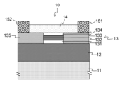
- the semiconductor device 10 is a semiconductor laser, and as shown in FIG. 1, includes a TiO2 layer (first layer) 12, an active layer (first core) 132, a first waveguide 13 made of an InP-based semiconductor, and a first cladding SiO2 layer 14, which are arranged in this order on a substrate 11.
- a Si substrate is used for the substrate 11.
- Other than a Si substrate, a sapphire substrate, a SiC substrate, etc. may also be used.
- the first layer 12 is disposed near the active layer (first core) 132 and can be optically coupled to the active layer 132.
- a layer made of benzocyclobutene (BCB) may be used instead of the TiO2 layer.
- a material having a negative thermo-optic coefficient may be used.
- the first waveguide 13 is composed of semiconductors (p-type semiconductor 134, n-type semiconductor 135) doped with n-type and p-type impurities, which are formed in a state where they sandwich the active layer (first core) 132, and electrodes 151 and 152 are formed on the p-type semiconductor 134 and the n-type semiconductor 135, respectively.
- it has a layer structure consisting of an i (intrinsic) type semiconductor layer 131, an active layer 132, and an i type semiconductor layer 133, a p type semiconductor 134 on one side of the layer structure, and an n type semiconductor 135 on the other side.
- a p type electrode 151 and an n type electrode 153 are provided on the surfaces of the p type semiconductor 134 and the n type semiconductor 135, respectively, and a cladding 14 is provided between the p type electrode 151 and the n type electrode 152.
- the active layer 132 is an InGaAsP-based multiple quantum well structure in the 1.55 ⁇ m wavelength band, with six quantum well layers.
- the thickness of the active layer 132 is 150 nm.
- Each i-layer is 50 nm thick and made of undoped InP.
- the p-type semiconductor 134 is, for example, Zn-doped (1 ⁇ 10 18 cm ⁇ 3 ) p-type InP
- the n-type semiconductor 135 is, for example, Si-doped (2 ⁇ 10 18 cm ⁇ 3 ) n-type InP.
- the semiconductor laser 10 may be provided with an optical feedback mechanism.
- the optical feedback mechanism may be a distributed feedback grating formed in a layer above the first waveguide 13.
- a semiconductor laser structure is formed by a layer structure including the active layer (first core) 132, the p-type semiconductor 134, the n-type semiconductor 135, the electrodes 151 and 152, and the optical feedback mechanism.
- the thickness of the first layer ( TiO2 layer) 12 may be, for example, about 100 nm, so that the light guided through the active layer (first core) 132 can leak and be optically coupled with the first layer ( TiO2 layer) 12. In other words, the intensity distribution of the light guided through the active layer (first core) 132 may overlap with the first layer ( TiO2 layer) 12.
- a SiO2 layer (second cladding) 112 is disposed between the Si substrate 11 and the first layer ( TiO2 layer) 12.
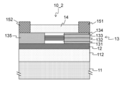
- a TiO 2 layer 122 may be disposed between the first waveguide 13 and the SiO 2 layer 14 of the first cladding.
- the temperature change of the oscillation wavelength of a DFB (Distributed Feedback) laser can be approximately expressed by equation (1), ignoring the linear expansion coefficient of the active layer and the carrier plasma effect.
- ⁇ Bragg is the Bragg wavelength of the DFB laser
- ⁇ III-V is the optical confinement coefficient of the III-V semiconductor
- n III-V is the refractive index of the III-V semiconductor
- dn III-V /dT is the thermo-optic coefficient of the III-V semiconductor
- ⁇ clad is the optical confinement coefficient of the first layer (TiO 2 layer or BCB layer)
- n clad is the refractive index of the first layer (TiO 2 layer or BCB layer)
- dn clad /dT is the thermo-optic coefficient of the first layer (TiO 2 layer or BCB layer).
- dn III-V /dT and dn clad /dT are positive values, d ⁇ /dT will not be 0 (zero). Usually, dn III-V /dT is a positive value. On the other hand, if dn clad /dT is a negative value, d ⁇ /dT can be reduced by adjusting the optical confinement factor in the design of the waveguide. In other words, the wavelength change with respect to temperature can be suppressed.
- TiO2 or BCB is known as a material with a negative thermo-optic coefficient (Yuki Atsumi et al., "Athermal Wavelength Characteristics of Si Slot Ring Resonator Embedded with Benzocyclobutene for Optoelectronic Integrated Circuits," 2010, Jpn. J. Appl. Phys. 49, 050206. Feng Qiu, Andrew M. Spring, Shiyoshi Yokoyama, "Athermal and high-Q hybrid TiO2-Si3N4 ring resonator via an etching-free fabrication technique," ACS Photonics, Vol. 2, No. 3, 18.03.2015, p. 405-409.).
- the horizontal axis in the figure is the thickness (t InP ) of the InP layer including the active layer (first core).
- the vertical axis in the figure is normalized with the value of ⁇ / ⁇ T being 1 when t InP is 0.25 ⁇ m.
- the calculation was performed using formula (1) for a structure in which one TiO2 film is arranged (FIG. 2) and a structure in which two TiO2 films are arranged (FIG. 3).
- the thickness of the TiO2 film was 0.1 ⁇ m and the thickness of the SiO2 was 3 ⁇ m.
- a structure without a TiO2 layer was also calculated.
- ⁇ / ⁇ T decreases with the decrease in the thickness t InP of the InP layer (dotted line in the figure). This is because, by thinning the InP layer, the optical confinement coefficient of the active layer (first core) made of a III-V group compound semiconductor with a high thermo-optic coefficient decreases, while the optical confinement coefficient of the SiO 2 layer with a low thermo-optic coefficient increases. Thus, even if the InP layer is thinned to a thickness of about 0.1 ⁇ m, ⁇ /dT only decreases to a value of about 80%.
- the optical confinement coefficient of the active layer (first core) made of a III-V group compound semiconductor with a high thermo-optic coefficient is reduced by thinning the InP layer, while the optical confinement coefficient of the TiO 2 layer with a negative thermo-optic coefficient is increased. In this way, the TiO 2 layer is optically coupled to the active layer (first core).
- the semiconductor device of the present embodiment by providing the first layer (TiO 2 layer or BCB layer) in the vicinity of the active layer, it is possible to suppress the change in wavelength due to the change in temperature.
- the semiconductor device 20 is a semiconductor laser, and as shown in FIG. 5, includes, on a Si substrate 11, a second waveguide composed of a second core 22 and a third cladding 21, a first waveguide 13 composed of an active layer (first core) 132 and an InP cladding, and a SiO 2 first cladding 14, in that order.
- the first waveguide 13 has the same configuration as in the first embodiment.
- the third cladding 21 is made of SiO 2.
- the third cladding 21_2 may be made of benzocyclobutene (BCB).
- the second core 22 is the first layer in the first embodiment and is made of TiO 2. Alternatively, it may be made of BCB (benzocyclobutene).
- the second core 22 is disposed near the first core 132 and positioned so that it can be optically coupled to the first core 132.
- the distance between the first core 132 and the second core 22 is approximately 100 to 500 nm.
- the width of the second core 22 be 0.3 ⁇ m or more and 3 ⁇ m or less.
- a supermode is formed between the first waveguide 13 and the second waveguide, making it possible to confine light in the cores of both waveguides.
- the semiconductor laser 20 may be provided with an optical feedback mechanism.
- the optical feedback mechanism may be a distributed feedback grating formed in a layer above the first waveguide 13.
- the horizontal axis in the figure is the thickness (t InP ) of the InP layer including the active layer (first core).
- the vertical axis in the figure is normalized with the value of ⁇ / ⁇ T set to 1 when t InP is 0.25 ⁇ m.
- the width of the TiO2 core was 1 ⁇ m and the thickness was 0.5 ⁇ m.
- the thickness of the SiO2 was 3 ⁇ m.
- the distance in the thickness direction between the TiO2 core and the first waveguide was 0.1 ⁇ m.
- the calculation result for the structure without the TiO2 layer is shown (dotted line in the figure. Same as the case without the TiO2 layer in FIG. 4).
- ⁇ / ⁇ T is 0.4%.
- ⁇ / ⁇ T is about 0%.
- the semiconductor device of the present embodiment by providing the first layer (TiO 2 layer or BCB layer) in the vicinity of the active layer, it is possible to suppress the change in wavelength due to the change in temperature.
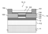
- the semiconductor device 30 is a semiconductor laser, and as shown in FIG. 8, includes, on a Si substrate 11, a second waveguide consisting of a second core 32 and a third clad 31, a first waveguide 13 consisting of a first core 132 and an InP clad, and a SiO 2 first clad 14, in that order.
- the first waveguide 13 has the same configuration as in the first embodiment.
- the third cladding 31 is made of SiO 2.
- it may be made of BCB (benzocyclobutene).
- the second core 32 is disposed near the first core 132 and positioned so that it can be optically coupled to the first core 132.
- the distance between the first core 132 and the second core 32 is approximately 100 to 500 nm.
- the second core 32 includes Si 321 and TiO 2 322.
- the TiO 2 322 is disposed at the center in the width direction, i.e., below the first core 132, and the Si 321 is disposed on both sides in the width direction of the TiO 2 322.
- the second core 32 has a so-called slot-type optical waveguide shape with the TiO 2 322 as a slot layer.
- the width of the TiO 2 slot layer 322 is 0.05 ⁇ m or more and 1 ⁇ m or less.
- a supermode is formed by arranging the first waveguide 13 and the second waveguide having the slot-type optical waveguide at a position where they can be optically coupled.
- the semiconductor laser 30 uses one slot layer 322, but this is not limiting, and as shown in FIG. 9, the semiconductor laser 30_2 may use two slot layers 322. Also, three or more slot layers may be used.
- the semiconductor laser 30 may be provided with an optical feedback mechanism.
- the optical feedback mechanism may be a distributed feedback grating formed in a layer above the first waveguide 13.
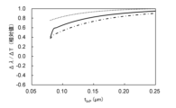
- the vertical axis in the figure is the thickness (t InP ) of the InP layer including the active layer (first core).
- the vertical axis in the figure is normalized with the value of ⁇ / ⁇ T set to 1 when t InP is 0.25 ⁇ m.
- the width of the TiO2 slot layer was 0.1 ⁇ m and the thickness was 1 ⁇ m.
- the thickness of the SiO2 was 2 ⁇ m.
- the distance in the thickness direction between the TiO2 slot layer and the first waveguide was 0.1 ⁇ m.
- the calculation result for a structure without a TiO2 layer is shown (dotted line in the figure. Same as the case without the TiO2 layer in FIG. 4).
- ⁇ / ⁇ T decreases when the InP layer thickness t InP is about 0.14 ⁇ m or less, and ⁇ / ⁇ T is about 40% when t InP is 0.08 to 0.13 ⁇ m (solid line in the figure).
- ⁇ / ⁇ T decreases when t InP is about 0.12 ⁇ m or less, and ⁇ / ⁇ T is about 0 when t InP is 0.08 to 0.10 ⁇ m (dotted line in the figure).
- the optical confinement coefficient of the active layer (first core) made of a III-V group compound semiconductor with a high thermo-optic coefficient is reduced, while the optical confinement coefficient of the TiO 2 slot layer with a negative thermo-optic coefficient is increased. In this way, the TiO 2 slot layer is optically coupled to the active layer (first core).
- SiO 2 is used as the cladding material of the second waveguide and TiO 2 is used as the material of the slot layer, but this is not limiting.
- BCB may be used as the cladding material and the slot layer material.
- the semiconductor device of the present embodiment by providing a TiO 2 slot layer or a BCB slot layer in the vicinity of the active layer, it is possible to suppress a change in wavelength due to a change in temperature.
- a structure in which a diffraction grating is formed on an active layer, i.e., a distributed feedback diffraction grating, is used as the optical feedback mechanism.
- a mirror is used as the optical feedback mechanism.
- the semiconductor device is a semiconductor laser, and includes a gain region (active layer region) and a mirror 40 .
- the gain region includes, on a Si substrate, a second cladding of SiO 2 , an active layer (first core) 132 , a first waveguide 13 composed of an InP cladding, and a first cladding of SiO 2 14 (not shown).
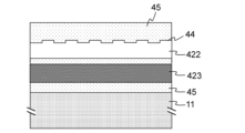
- the mirror 40 is integrated on the same Si substrate 11 as the gain region, and as shown in FIGS. 12A to 12C, includes, on the Si substrate 11, a fourth cladding SiO 2 41, a reflective waveguide 42 made of InP 422 and TiO 2 421, and a fifth cladding SiO 2 43, in that order.
- the reflective waveguide 42 is optically connected (butt jointed) to the first waveguide 13 in the gain region.
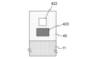
- the reflective waveguide 42 includes a TiO2 clad layer 421 on both the lower surface (surface on the fourth clad 41 side) and the upper surface (surface on the fifth clad 43 side) of an InP core layer 422.
- the thermo-optic coefficient of InP is a positive value
- the thermo-optic coefficient of TiO2 is a negative value.
- the InP core layer 422 includes a diffraction grating 44 on the upper or lower surface.
- the temperature change in the refractive index of the InP core 422 and the TiO2 cladding 421 is offset, and the temperature dependence is reduced. Therefore, the temperature dependence of the mirror 40 having this reflective waveguide 42 is reduced.
- a semiconductor laser that is typically composed of a gain region and an external mirror (e.g., a DBR mirror)
- the reflection wavelength of the external mirror depends on temperature
- the oscillation wavelength of the semiconductor laser will change with temperature.
- the semiconductor device semiconductor laser
- semiconductor laser can reduce the temperature dependency of the reflection wavelength of the mirror 40, thereby reducing the change in the oscillation wavelength of the semiconductor laser due to temperature changes.
- the semiconductor device may have a configuration including a SiO 2 cladding 45 including a TiO 2 core waveguide 423 between the Si substrate 11 and an InP core waveguide 422 having a diffraction grating 44.
- a supermode is formed by the InP core waveguide 422 and the TiO 2 core waveguide 423, the temperature dependency of the reflection wavelength of the mirror 40_2 is reduced, and the change in the oscillation wavelength of the semiconductor laser due to temperature change is reduced.
- the gain region may include a layer made of a material having a negative thermo-optic coefficient (e.g., TiO2 or BCB) as in the first to third embodiments. This can further reduce the change in the oscillation wavelength of the semiconductor laser due to temperature changes.
- a negative thermo-optic coefficient e.g., TiO2 or BCB
- an example of use in a semiconductor laser is shown, but it may also be used in other semiconductor devices such as modulators, semiconductor optical amplifiers, and light receiving devices.
- a semiconductor device comprising, in order, a substrate, a first waveguide including an active layer, and a first cladding, and further comprising a first layer made of a material having a negative thermo-optic coefficient in the vicinity of the active layer, and a current is injected into the active layer in a lateral direction that is parallel to the surface of the substrate and perpendicular to the waveguide direction.
- Appendix 2 The semiconductor device described in Appendix 1 further includes a second clad, and the second clad and the first layer are disposed between the substrate and the first waveguide, in that order from the substrate.
- Appendix 3 The semiconductor device according to appendix 1 or 2, further comprising a fourth layer between the active layer and the first cladding, the fourth layer being made of a material having a negative thermo-optic coefficient.
- the semiconductor device described in Appendix 1 further includes a third clad covering the first layer, the first layer and the third clad forming a second waveguide, and the second waveguide is arranged to be optically coupled to the first waveguide.
- the semiconductor device described in Appendix 4 further includes a third layer made of a material having a higher refractive index than the first layer on a surface of the first layer perpendicular to the lateral direction, and the first layer and the third layer form a slot-type optical waveguide.
- a semiconductor device comprising, in order, a gain region including a substrate, a first waveguide including an active layer, and a first clad; and, in order, the substrate, a fourth clad, a semiconductor waveguide having an optical feedback structure, and a fifth clad; and a mirror further comprising a fourth layer made of a material having a negative thermo-optic coefficient arranged so as to be optically coupled to the semiconductor waveguide, wherein a current is injected into the active layer in a lateral direction parallel to the surface of the substrate and perpendicular to the waveguide direction, so that the active layer and the semiconductor waveguide are optically connected.
- Appendix 7 The semiconductor device described in Appendix 6, in which the optical feedback structure is a diffraction grating and the fourth layer is disposed so as to cover the semiconductor waveguide.
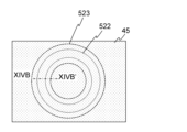
- Appendix 8 The semiconductor device described in Appendix 6, in which the optical feedback structure is a diffraction grating and the fourth layer is disposed within the fourth cladding.
- Appendix 9 The semiconductor device described in Appendix 6, in which the optical feedback structure is a ring resonator and the fourth layer is disposed within the fourth cladding.
- Appendix 10 The semiconductor device described in appendix 1 or 2, in which the first layer is disposed between the substrate and the first waveguide and in contact with the first waveguide, and the thickness of the first waveguide is 0.08 ⁇ m or more and 0.13 ⁇ m or less.
- Appendix 11 The semiconductor device described in appendix 4 or appendix 5, in which the distance between the first waveguide and the second waveguide is 100 nm or more and 500 nm or less, and the thickness of the first waveguide is 0.08 ⁇ m or more and 0.14 ⁇ m or less.
- Appendix 12 The semiconductor device described in appendix 4 or appendix 5, in which the distance between the first waveguide and the second waveguide is 100 nm or more and 500 nm or less, the thickness of the first waveguide is 0.08 ⁇ m or more and 0.13 ⁇ m or less, and the width of the first layer is 0.3 ⁇ m or more and 3 ⁇ m or less.
- the present invention relates to a semiconductor device and can be applied to optical communication devices and optical communication systems.
Landscapes
- Physics & Mathematics (AREA)
- Condensed Matter Physics & Semiconductors (AREA)
- General Physics & Mathematics (AREA)
- Electromagnetism (AREA)
- Optics & Photonics (AREA)
- Geometry (AREA)
- Semiconductor Lasers (AREA)
Priority Applications (2)
| Application Number | Priority Date | Filing Date | Title |
|---|---|---|---|
| JP2025532321A JPWO2025013241A1 (https=) | 2023-07-12 | 2023-07-12 | |
| PCT/JP2023/025725 WO2025013241A1 (ja) | 2023-07-12 | 2023-07-12 | 半導体装置 |
Applications Claiming Priority (1)
| Application Number | Priority Date | Filing Date | Title |
|---|---|---|---|
| PCT/JP2023/025725 WO2025013241A1 (ja) | 2023-07-12 | 2023-07-12 | 半導体装置 |
Publications (1)
| Publication Number | Publication Date |
|---|---|
| WO2025013241A1 true WO2025013241A1 (ja) | 2025-01-16 |
Family
ID=94214801
Family Applications (1)
| Application Number | Title | Priority Date | Filing Date |
|---|---|---|---|
| PCT/JP2023/025725 Pending WO2025013241A1 (ja) | 2023-07-12 | 2023-07-12 | 半導体装置 |
Country Status (2)
| Country | Link |
|---|---|
| JP (1) | JPWO2025013241A1 (https=) |
| WO (1) | WO2025013241A1 (https=) |
Citations (6)
| Publication number | Priority date | Publication date | Assignee | Title |
|---|---|---|---|---|
| JP2013165095A (ja) * | 2012-02-09 | 2013-08-22 | Nippon Telegr & Teleph Corp <Ntt> | 半導体薄膜レーザ |
| JP2016171173A (ja) * | 2015-03-12 | 2016-09-23 | 日本電信電話株式会社 | 半導体光素子 |
| US20180241176A1 (en) * | 2017-02-22 | 2018-08-23 | International Business Machines Corporation | Electro-optical device with asymmetric, vertical current injection ohmic contacts |
| JP2019083268A (ja) * | 2017-10-31 | 2019-05-30 | 日本電信電話株式会社 | 半導体レーザ |
| JP2020519011A (ja) * | 2017-05-05 | 2020-06-25 | インターナショナル・ビジネス・マシーンズ・コーポレーションInternational Business Machines Corporation | Iii−v族利得材料および集積化ヒート・シンクを有する電子−光学装置ならびにその製造方法 |
| US20210226409A1 (en) * | 2020-01-17 | 2021-07-22 | Nokia Solutions And Networks Oy | Reflective optical modulator having reduced temperature sensitivity |
-
2023
- 2023-07-12 JP JP2025532321A patent/JPWO2025013241A1/ja active Pending
- 2023-07-12 WO PCT/JP2023/025725 patent/WO2025013241A1/ja active Pending
Patent Citations (6)
| Publication number | Priority date | Publication date | Assignee | Title |
|---|---|---|---|---|
| JP2013165095A (ja) * | 2012-02-09 | 2013-08-22 | Nippon Telegr & Teleph Corp <Ntt> | 半導体薄膜レーザ |
| JP2016171173A (ja) * | 2015-03-12 | 2016-09-23 | 日本電信電話株式会社 | 半導体光素子 |
| US20180241176A1 (en) * | 2017-02-22 | 2018-08-23 | International Business Machines Corporation | Electro-optical device with asymmetric, vertical current injection ohmic contacts |
| JP2020519011A (ja) * | 2017-05-05 | 2020-06-25 | インターナショナル・ビジネス・マシーンズ・コーポレーションInternational Business Machines Corporation | Iii−v族利得材料および集積化ヒート・シンクを有する電子−光学装置ならびにその製造方法 |
| JP2019083268A (ja) * | 2017-10-31 | 2019-05-30 | 日本電信電話株式会社 | 半導体レーザ |
| US20210226409A1 (en) * | 2020-01-17 | 2021-07-22 | Nokia Solutions And Networks Oy | Reflective optical modulator having reduced temperature sensitivity |
Also Published As
| Publication number | Publication date |
|---|---|
| JPWO2025013241A1 (https=) | 2025-01-16 |
Similar Documents
| Publication | Publication Date | Title |
|---|---|---|
| JP5897414B2 (ja) | 光デバイスの製造方法 | |
| US9312663B2 (en) | Laser device, light modulation device, and optical semiconductor device | |
| US9088132B2 (en) | Semiconductor optical element, integrated semiconductor optical element, and semiconductor optical element module | |
| US8457452B2 (en) | Integrated semiconductor optical device | |
| JP5882287B2 (ja) | 波長可変フィルタ及び波長可変レーザモジュール | |
| US20070133647A1 (en) | Wavelength modulated laser | |
| KR20110126661A (ko) | 하이브리드 수직공진 레이저 | |
| WO2007080891A1 (ja) | 半導体レーザ、モジュール、及び、光送信機 | |
| JP6510391B2 (ja) | 半導体レーザ | |
| US8472760B2 (en) | Integrated semiconductor optical device | |
| JP2003014963A (ja) | 半導体光集積素子とその製造方法並びに光通信用モジュール | |
| JP6588859B2 (ja) | 半導体レーザ | |
| JP2019008179A (ja) | 半導体光素子 | |
| US7949020B2 (en) | Semiconductor laser and optical integrated semiconductor device | |
| US9952390B2 (en) | Optical element, optical module, and optical transmission system | |
| US12212120B2 (en) | Tunable Vernier effect laser emission device | |
| JP6483521B2 (ja) | 半導体レーザ | |
| JP2011086714A (ja) | 波長可変レーザ | |
| WO2025013241A1 (ja) | 半導体装置 | |
| US20250047069A1 (en) | Semiconductor Laser | |
| US20250055254A1 (en) | Semiconductor Laser | |
| JP7294453B2 (ja) | 直接変調レーザ | |
| JP6927153B2 (ja) | 半導体レーザ | |
| WO2022211061A1 (ja) | 波長可変レーザ | |
| JP2000223784A (ja) | 波長安定化半導体レーザー |
Legal Events
| Date | Code | Title | Description |
|---|---|---|---|
| 121 | Ep: the epo has been informed by wipo that ep was designated in this application |
Ref document number: 23945116 Country of ref document: EP Kind code of ref document: A1 |
|
| ENP | Entry into the national phase |
Ref document number: 2025532321 Country of ref document: JP Kind code of ref document: A |
|
| WWE | Wipo information: entry into national phase |
Ref document number: 2025532321 Country of ref document: JP |
|
| NENP | Non-entry into the national phase |
Ref country code: DE |