WO2025009015A1 - パワーモジュール及びその製造方法並びに電力変換装置 - Google Patents
パワーモジュール及びその製造方法並びに電力変換装置 Download PDFInfo
- Publication number
- WO2025009015A1 WO2025009015A1 PCT/JP2023/024607 JP2023024607W WO2025009015A1 WO 2025009015 A1 WO2025009015 A1 WO 2025009015A1 JP 2023024607 W JP2023024607 W JP 2023024607W WO 2025009015 A1 WO2025009015 A1 WO 2025009015A1
- Authority
- WO
- WIPO (PCT)
- Prior art keywords
- conductive
- pattern
- conductive pattern
- connection member
- terminal
- Prior art date
- Legal status (The legal status is an assumption and is not a legal conclusion. Google has not performed a legal analysis and makes no representation as to the accuracy of the status listed.)
- Pending
Links
Images


Classifications
-
- H—ELECTRICITY
- H10—SEMICONDUCTOR DEVICES; ELECTRIC SOLID-STATE DEVICES NOT OTHERWISE PROVIDED FOR
- H10W—GENERIC PACKAGES, INTERCONNECTIONS, CONNECTORS OR OTHER CONSTRUCTIONAL DETAILS OF DEVICES COVERED BY CLASS H10
- H10W70/00—Package substrates; Interposers; Redistribution layers [RDL]
- H10W70/60—Insulating or insulated package substrates; Interposers; Redistribution layers
-
- H—ELECTRICITY
- H10—SEMICONDUCTOR DEVICES; ELECTRIC SOLID-STATE DEVICES NOT OTHERWISE PROVIDED FOR
- H10W—GENERIC PACKAGES, INTERCONNECTIONS, CONNECTORS OR OTHER CONSTRUCTIONAL DETAILS OF DEVICES COVERED BY CLASS H10
- H10W72/00—Interconnections or connectors in packages
-
- H—ELECTRICITY
- H10—SEMICONDUCTOR DEVICES; ELECTRIC SOLID-STATE DEVICES NOT OTHERWISE PROVIDED FOR
- H10W—GENERIC PACKAGES, INTERCONNECTIONS, CONNECTORS OR OTHER CONSTRUCTIONAL DETAILS OF DEVICES COVERED BY CLASS H10
- H10W90/00—Package configurations
Definitions
- This disclosure relates to a power module, a manufacturing method thereof, and a power conversion device.
- Patent Document 1 JP 2001-237359 A discloses a power semiconductor device that includes a semiconductor chip, a terminal metal fitting, and a resin case frame to which the terminal metal fitting is fixed.
- the terminal metal fitting includes a first electrode and a second electrode that is disposed at the tip of the terminal metal fitting relative to the first electrode.
- the electrical connection between the semiconductor chip and the terminal metal fitting can be selected between soldering between the second electrode and the semiconductor chip, and bonding wire between the first electrode and the semiconductor chip.
- the objective of this disclosure is to provide a power module and a power conversion device with improved reliability.
- the power module of the present disclosure comprises a circuit board, a semiconductor element, a terminal, and a first conductive connection member.
- the circuit board includes an insulating layer having a main surface, and a conductive circuit pattern provided on the main surface.
- the semiconductor element is bonded to the conductive circuit pattern.
- the conductive circuit pattern includes a first conductive pattern.
- the terminal includes a first end. The first end of the terminal includes a first surface bonded to the first conductive pattern and a second surface opposite the first surface.
- the first conductive connection member is bridged between the second surface and the first conductive pattern.
- the method for manufacturing a power module of the present disclosure includes preparing a circuit board.
- the circuit board includes an insulating layer having a main surface and a conductive circuit pattern provided on the main surface.
- the conductive circuit pattern includes a first conductive pattern.
- the method for manufacturing a power module of the present embodiment includes joining a semiconductor element to the conductive circuit pattern and joining a terminal to the first conductive pattern.
- the terminal includes a first end.
- the first end of the terminal includes a first surface joined to the first conductive pattern and a second surface opposite the first surface.
- the method for manufacturing a power module of the present embodiment includes bridging a first conductive connection member between the second surface and the first conductive pattern.
- the power conversion device disclosed herein has a power module disclosed herein, and is equipped with a main conversion circuit that converts and outputs input power, and a control circuit that outputs a control signal to the main conversion circuit to control the main conversion circuit.
- the terminal is electrically connected to the first conductive pattern not only by the joint between the first surface of the terminal and the first conductive pattern, but also by the first conductive connection member. Therefore, even if the joint is peeled off from the first conductive pattern, the terminal continues to be electrically connected to the first conductive pattern through the first conductive connection member.
- the power module and power conversion device disclosed herein have improved reliability.
- FIG. 1 is a schematic cross-sectional view of a power module according to a first embodiment.
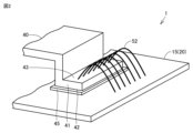
- 1 is a schematic partially enlarged perspective view of a power module according to a first embodiment;
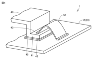
- 1 is a schematic partially enlarged plan view of a power module according to a first embodiment of the present invention;
- FIG. 2 is a flowchart showing a method for manufacturing the power module according to the first embodiment.
- FIG. 11 is a schematic partially enlarged perspective view of a power module according to a modified example of the first embodiment.
- FIG. 11 is a schematic partially enlarged plan view of a power module according to a modified example of the first embodiment.
- FIG. 11 is a schematic partially enlarged plan view of a power module according to a second embodiment.
- FIG. 11 is a schematic partial enlarged plan view of a power module according to a first modified example of the second embodiment.
- FIG. 13 is a schematic partial enlarged plan view of a power module according to a second modified example of the second embodiment.
- FIG. 11 is a schematic partially enlarged plan view of a power module according to a third embodiment.
- FIG. 11 is a schematic partially enlarged perspective view of a power module according to a third embodiment.
- Embodiment 1 A power module 1 according to a first embodiment will be described with reference to Figures 1 to 3.
- the power module 1 includes a circuit board 12, semiconductor elements 30 and 31, a terminal 40, and conductive connection members 50, 51, and 52.
- the power module 1 may further include a base plate 10, a case 60, and a sealing member 61.
- the base plate 10 supports the circuit board 12.
- the base plate 10 dissipates heat generated in the power module 1 to the outside of the power module 1.
- the base plate 10 is formed of, for example, copper (Cu) or silicon carbide particle reinforced aluminum composite (AlSiC).
- the base plate 10 may be provided with cooling fins (not shown).
- the circuit board 12 includes an insulating layer 13 and a conductive circuit pattern 15.
- the circuit board 12 may further include a conductor pattern 14.
- the insulating layer 13 is formed of an insulating material such as alumina (Al 2 O 3 ), aluminum nitride (AlN), resin, or filler-containing resin.
- the insulating layer 13 has a main surface 13a and a main surface 13b opposite to the main surface 13a.
- the conductor pattern 14 is provided on the main surface 13a.
- the conductive circuit pattern 15 is provided on the main surface 13b.
- the conductive circuit pattern 15 includes a conductive pattern 20.
- the conductive pattern 20 is, for example, a conductive pad for bonding to which the terminal 40 is bonded.
- the conductive pattern 20 may be spaced apart from the portion of the conductive circuit pattern 15 to which the semiconductor elements 30 and 31 are bonded.
- the conductor pattern 14 and the conductive circuit pattern 15 are formed of a conductive material such as copper (Cu) or aluminum (Al).
- the conductor pattern 14 and the conductive circuit pattern 15 may have a two-layer structure including an aluminum (Al) layer in contact with the insulating layer 13 and a copper (Cu) layer provided on the aluminum (Al) layer.
- the surface of the conductive circuit pattern 15 may be provided with an uneven structure or coating to improve adhesion between the conductive circuit pattern 15 and the sealing member 61.
- the circuit board 12 is fixed to the base plate 10 at the joint 11.
- the conductor pattern 14 is joined to the base plate 10 at the joint 11.
- the joint 11 may be formed, for example, from solder, a metal microparticle sintered body such as a silver microparticle sintered body, or a resin containing a conductive filler, or may be liquid phase diffusion bonding between the conductor pattern 14 and the base plate 10.
- the semiconductor elements 30 and 31 are, for example, power semiconductor elements. Specifically, the semiconductor elements 30 and 31 are switching elements such as insulated gate bipolar transistors (IGBTs) or metal oxide semiconductor field effect transistors (MOSFETs), or rectifying elements such as Schottky barrier diodes.
- the semiconductor elements 30 and 31 are formed of silicon (Si) or a wide bandgap semiconductor material having a bandgap larger than that of silicon (Si).
- the wide bandgap semiconductor material is, for example, silicon carbide (SiC), gallium nitride (GaN)-based material, or diamond.
- the semiconductor elements 30 and 31 have electrodes.
- the electrodes of the semiconductor elements 30 and 31 are formed of, for example, aluminum (Al) or an aluminum alloy with added silicon (Si).
- a coating layer such as a nickel (Ni) layer or a gold (Au) layer may be provided on the electrodes of the semiconductor elements 30 and 31.
- the semiconductor element 30 is joined to the conductive circuit pattern 15 at a joint 33.
- the semiconductor element 31 is joined to the conductive circuit pattern 15 at a joint 34.
- the joints 33 and 34 may be formed, for example, from solder, a metal microparticle sintered body such as a silver microparticle sintered body, or a resin containing a conductive filler, or may be liquid phase diffusion bonding between the electrodes of the semiconductor elements 30 and 31 and the conductive circuit pattern 15.
- the terminal 40 extends to the outside of the case 60.
- the current from the power module 1 is taken out to the outside of the power module 1 through the terminal 40.
- the terminal 40 is formed of a conductive material such as copper (Cu) or aluminum (Al).
- a coating layer (not shown) such as a nickel (Ni) layer or a gold (Au) layer may be provided on the surface of the terminal 40.
- the terminal 40 includes a first end 41.
- the first end 41 is an end of the terminal 40 that is proximal to the circuit board 12.
- the first end 41 includes a first surface 42 and a second surface 43 opposite the first surface 42.
- the first surface 42 of the terminal 40 is joined to the conductive pattern 20 at a joint 45.
- the joint 45 may be formed, for example, from solder, a metal microparticle sintered body such as a silver microparticle sintered body, or a resin containing a conductive filler, or may be liquid phase diffusion bonding between the first surface 42 of the terminal 40 and the conductive pattern 20.
- the terminal 40 is an outsert-type terminal that can be easily separated from the case 60.
- the terminal 40 may also be an insert-type terminal that is integrated into the case 60.
- the conductive connection members 50, 51, and 52 are formed of a conductive material such as aluminum (Al) or copper (Cu).
- the conductive connection member 50 spans the semiconductor element 30 and the conductive pattern 20.
- the conductive connection member 50 is, for example, a conductive wire bonded to the electrode of the semiconductor element 30 and the conductive pattern 20.
- the conductive connection member 50 may be a conductive plate bonded to the electrode of the semiconductor element 30 and the conductive pattern 20 using a bonding member such as solder.
- the conductive connection member 51 spans the semiconductor element 30 and the semiconductor element 31.
- the conductive connection member 51 is, for example, a conductive wire bonded to the electrode of the semiconductor element 30 and the electrode of the semiconductor element 31.
- the conductive connection member 52 spans the conductive pattern 20 and the second surface 43 of the first end 41 of the terminal 40.
- the conductive connection member 52 is, for example, a conductive wire bonded to the conductive pattern 20 and the second surface 43 of the first end 41 of the terminal 40.
- the case 60 protects the circuit board 12 and the semiconductor elements 30, 31.
- the case 60 is fixed to the base plate 10 using an adhesive (not shown).
- the case 60 is formed of an insulating resin such as epoxy resin or polyphenylene sulfide resin.
- the sealing member 61 seals the semiconductor elements 30, 31.
- the sealing member 61 is formed of, for example, a thermosetting resin such as an epoxy resin, silicone gel, or an insulating resin containing a metal or a filler.
- the semiconductor elements 30, 31, which are formed of a wide band gap semiconductor material, can reach a high temperature of approximately 200°C during operation of the semiconductor elements 30, 31.
- an insulating resin containing a metal or a filler as the material for the sealing member 61, the sealing member 61 is prevented from softening or deteriorating even at such high temperatures. A decrease in the reliability of the joints of the conductive connection members 50, 51, 52 can be prevented.
- the sealing member 61 may have a multi-layer structure including a first sealing layer (not shown) that covers the joints between the semiconductor elements 30, 31 and the conductive connection members 50, 51, and a second sealing layer (not shown) that is provided on the first sealing layer, the circuit board 12, the semiconductor elements 30, 31, and the base plate 10.
- the first sealing layer is made of a material harder than the second sealing layer, and reinforces the joints between the semiconductor elements 30, 31 and the conductive connection members 50, 51.
- the first sealing layer is made of epoxy resin
- the second sealing layer is made of gel or the like.
- the manufacturing method of the power module 1 of the present embodiment includes preparing a circuit board 12 (S1).
- the circuit board 12 includes an insulating layer 13 and a conductive circuit pattern 15.
- the insulating layer 13 has a main surface 13b.
- the conductive circuit pattern 15 is provided on the main surface 13b.
- the conductive circuit pattern 15 includes a conductive pattern 20.
- the circuit board 12 may further include a conductor pattern 14.
- the manufacturing method of the power module 1 of this embodiment includes joining the semiconductor elements 30, 31 to the circuit board 12 (S2).
- the semiconductor elements 30, 31 are joined to the conductive circuit pattern 15 at the joints 33, 34.
- the manufacturing method of the power module 1 of this embodiment includes fixing the circuit board 12 to the base plate 10 (S3).
- the conductor pattern 14 of the circuit board 12 is joined to the base plate 10 at the joint 11.
- the manufacturing method of the power module 1 of this embodiment includes joining the terminal 40 to the conductive pattern 20 (S4).
- the terminal 40 includes a first end 41.
- the first end 41 of the terminal 40 includes a first surface 42 and a second surface 43 opposite the first surface 42.
- the first surface 42 is joined to the conductive pattern 20.
- the joint 45 between the terminal 40 and the conductive pattern 20 may be formed, for example, by solder, a metal microparticle sintered body such as a silver microparticle sintered body, or a resin containing a conductive filler, or may be liquid phase diffusion bonding between the first surface 42 of the terminal 40 and the conductive pattern 20.
- the manufacturing method of the power module 1 of this embodiment includes attaching the case 60 to the base plate 10 (S5).
- the case 60 is fixed to the base plate 10 using an adhesive (not shown).
- the manufacturing method of the power module 1 of this embodiment includes providing conductive connection members 50, 51 (S6).
- the conductive connection member 50 is bridged between the conductive pattern 20 and the semiconductor element 30.
- the conductive connection member 50 is connected to the conductive pattern 20 and the semiconductor element 30. If the conductive connection member 50 is a conductive wire, the conductive wire is bonded to the conductive pattern 20 and the semiconductor element 30.
- the conductive connection member 50 is bridged between the semiconductor element 30 and the semiconductor element 31.
- the conductive connection member 51 is connected to the semiconductor element 30 and the semiconductor element 31. If the conductive connection member 51 is a conductive wire, the conductive wire is bonded to the semiconductor element 30 and the semiconductor element 31.
- the manufacturing method of the power module 1 of this embodiment includes bridging the conductive connection member 52 between the second surface 43 of the terminal 40 and the conductive pattern 20 (S7).
- the conductive connection member 52 is connected to the second surface 43 of the terminal 40 and the conductive pattern 20. If the conductive connection member 52 is a conductive wire, the conductive wire is bonded to the second surface 43 of the terminal 40 and the conductive pattern 20.
- the manufacturing method of the power module 1 of this embodiment includes providing a sealing member 61 (S8).
- the sealing member 61 is provided by applying a sealing material to the space surrounded by the case 60 and the base plate 10.
- the sealing member 61 may have a multi-layer structure including a first sealing layer (not shown) and a second sealing layer (not shown).
- a first sealing material may be applied to the connection between the semiconductor elements 30, 31 and the conductive connecting members 50, 51, and then a second sealing material may be applied onto the first sealing material, the circuit board 12, the semiconductor elements 30, 31, and the base plate 10, thereby forming the sealing member 61 having a multi-layer structure.
- Steps S2 and S3 may be performed simultaneously. Step S3 may be performed before step S2. If the conductive connection members 50, 51, and 52 are the same conductive connection member, steps S6 and S7 may be performed simultaneously.
- the operation of the power module 1 of this embodiment will now be described.
- heat is generated from the semiconductor elements 30 and 31, and the semiconductor elements 30 and 31, the terminals 40, and the joints 45 become hot.
- no heat is generated from the semiconductor elements 30 and 31, and the semiconductor elements 30 and 31, the terminals 40, and the joints 45 become cold. Due to such temperature cycles, thermal stress is repeatedly applied to the joints 45. Cracks are generated from the ends of the joints 45, and these cracks propagate into the joints 45. As a result, the joints 45 may peel off from the conductive pattern 20.
- the terminal 40 is electrically connected to the conductive pattern 20 not only by the joint 45 but also by the conductive connection member 52.
- the conductive connection member 52 is bridged between the second surface 43 of the terminal 40 and the conductive pattern 20 and is deformable. Since the conductive connection member 52 deforms in response to temperature cycles, the thermal stress acting on the joint between the conductive connection member 52 and the terminal 40 and the joint between the conductive connection member 52 and the conductive pattern 20 is reduced.
- the joint between the conductive connection member 52 and the terminal 40 and the joint between the conductive connection member 52 and the conductive pattern 20 have higher durability against temperature cycles than the joint 45. Therefore, even if the joint 45 is peeled off from the conductive pattern 20, the terminal 40 continues to be electrically connected to the conductive pattern 20 through the conductive connection member 52.
- the power module 1 can be prevented from breaking down.
- the current flowing through the joint 45 is reduced. This suppresses the temperature rise of the joint 45 during operation of the power module 1, making the joint 45 less likely to peel off from the conductive pattern 20. This can suppress breakdowns in the power module 1.
- the terminal 40, the conductive pattern 20, and the conductive connection member 52 are made of the same material, the thermal stress acting on the joint between the conductive connection member 52 and the terminal 40 and the joint between the conductive connection member 52 and the conductive pattern 20 is further reduced. Therefore, even if the joint 45 peels off from the conductive pattern 20, the terminal 40 continues to be electrically connected to the conductive pattern 20 through the conductive connection member 52. This can prevent the power module 1 from failing.
- the terminal 40, the conductive pattern 20, and the conductive connection member 52 are made of copper (Cu), the terminal 40, the conductive pattern 20, and the conductive connection member 52 have the same hardness. Therefore, even if the conductive connection member 52 is joined to the terminal 40 and the conductive pattern 20 by ultrasonic bonding, the terminal 40 and the conductive pattern 20 are not gouged out by the conductive connection member 52, and the conductive connection member 52 is well joined to the terminal 40 and the conductive pattern 20. The reliability of the joint between the conductive connection member 52 and the terminal 40 and the joint between the conductive connection member 52 and the conductive pattern 20 is improved. The reliability of the power module 1 is improved.
- the bonding area of the joint 45 is larger than the bonding area between the terminal 40 and the conductive connection member 52 and the bonding area between the conductive connection member 52 and the conductive pattern 20. If there is no crack in the joint 45, the electrical resistance between the terminal 40 and the conductive pattern 20 via the joint 45 is smaller than the electrical resistance between the terminal 40 and the conductive pattern 20 via the conductive connection member 52. Therefore, when a crack develops in the joint 45, the electrical resistance between the terminal 40 and the conductive pattern 20 increases. Also, when the joint 45 peels off from the conductive pattern 20, the electrical resistance between the terminal 40 and the conductive pattern 20 increases rapidly. For example, deterioration of the joint 45 can be detected by monitoring the electrical resistance between the conductive pattern 20 and the portion of the terminal 40 that extends outside the case 60.
- the conductive connection member 52 may be a conductive ribbon. Also, the base plate 10 and the joint 11 may be omitted, and the conductor pattern 14 may function as the base plate 10.
- the power module 1 of this embodiment includes a circuit board 12, a semiconductor element 30, a terminal 40, and a first conductive connection member (conductive connection member 52).
- the circuit board 12 includes an insulating layer 13 having a main surface 13b, and a conductive circuit pattern 15 provided on the main surface 13b.
- the semiconductor element 30 is bonded to the conductive circuit pattern 15.
- the conductive circuit pattern 15 includes a first conductive pattern (conductive pattern 20).
- the terminal 40 includes a first end 41.
- the first end 41 of the terminal 40 includes a first surface 42 bonded to the first conductive pattern and a second surface 43 opposite to the first surface 42.
- the first conductive connection member is bridged between the second surface 43 of the terminal 40 and the first conductive pattern.
- the terminal 40 is electrically connected to the first conductive pattern (conductive pattern 20) not only by the joint 45 between the first surface 42 of the terminal 40 and the first conductive pattern, but also by the first conductive connection member (conductive connection member 52). Therefore, even if the joint 45 is peeled off from the first conductive pattern, the terminal 40 continues to be electrically connected to the first conductive pattern through the first conductive connection member. This improves the reliability of the power module 1.
- the terminals 40 are joined to the first conductive pattern (conductive pattern 20) rather than to the semiconductor elements 30. Therefore, even if the number of semiconductor elements 30 is increased to increase the capacity of the power module 1, the increase in manufacturing effort related to joining the terminals 40 can be suppressed. The manufacturing efficiency of the power module 1 is improved.
- the first conductive connection member (conductive connection member 52) is joined to the terminal 40 on the second surface 43 of the terminal 40, which is opposite to the first surface 42 of the terminal 40 that is joined to the first conductive pattern (conductive pattern 20). Therefore, the terminal 40 can be made smaller, and the power module 1 can be made smaller.
- the first conductive connection member (conductive connection member 52) is a conductive wire or a conductive ribbon.
- the terminal 40 continues to be electrically connected to the first conductive pattern through the first conductive connection member (conductive connection member 52). This improves the reliability of the power module 1.
- the first conductive pattern (conductive pattern 20), the terminal 40, and the first conductive connection member (conductive connection member 52) are made of copper (Cu).
- the first conductive pattern (conductive pattern 20) and the terminal 40 are made of copper (Cu), even if the first conductive connection member (conductive connection member 52) is made of copper (Cu), which has a higher strength than aluminum, the first conductive connection member can be joined or bonded well to the first conductive pattern and the terminal 40. Since a material with higher strength and higher reliability can be used as the material for the first conductive connection member, the reliability of the power module 1 is improved.
- the manufacturing method of the power module 1 of this embodiment includes preparing a circuit board 12 (S1).
- the circuit board 12 includes an insulating layer 13 having a main surface 13b and a conductive circuit pattern 15 provided on the main surface 13b.
- the conductive circuit pattern 15 includes a first conductive pattern (conductive pattern 20).
- the manufacturing method of the power module 1 of this embodiment includes joining a semiconductor element 30 to the conductive circuit pattern 15 (S2) and joining a terminal 40 to the first conductive pattern (S4).
- the terminal 40 includes a first end 41.
- the first end 41 of the terminal 40 includes a first surface 42 joined to the first conductive pattern and a second surface 43 opposite to the first surface 42.
- the manufacturing method of the power module 1 of this embodiment includes bridging a first conductive connection member between the second surface 43 of the terminal 40 and the first conductive pattern (S7).
- the terminal 40 continues to be electrically connected to the first conductive pattern through the first conductive connection member (conductive connection member 52). This improves the reliability of the power module 1.
- Embodiment 2 A power module 1 according to a second embodiment will be described with reference to Fig. 7.
- the power module 1 according to the present embodiment has a similar configuration to the power module 1 according to the first embodiment and achieves the same effects, but differs mainly in the following respects.
- the conductive circuit pattern 15 further includes a conductive pattern 21 and a conductive pattern 22.
- the conductive patterns 20, 21, and 22 are spaced apart from one another.
- the conductive patterns 21 and 22 may be spaced apart from the portions of the conductive circuit pattern 15 to which the semiconductor elements 30 and 31 are bonded.
- the conductive pattern 20 is, for example, a bonding conductive pad to which the terminal 40 is bonded.
- the conductive patterns 21 and 22 are, for example, conductive pads for testing.
- the power module 1 of this embodiment further includes conductive connection members 53, 54.
- the conductive connection member 53 is bridged between the conductive pattern 21 and the second surface 43 of the first end 41 of the terminal 40.
- the conductive connection member 53 is, for example, a conductive wire bonded to the conductive pattern 21 and the second surface 43 of the first end 41 of the terminal 40.
- the conductive connection member 54 is bridged between the conductive pattern 20 and the conductive pattern 22.
- the conductive connection member 54 is, for example, a conductive wire bonded to the conductive pattern 20 and the conductive pattern 22.
- the bonding area of the joint 45 is larger than the bonding area between the terminal 40 and the conductive connection member 52 and the bonding area between the conductive connection member 52 and the conductive pattern 20.
- the electrical resistance between the terminal 40 and the conductive pattern 20 via the joint 45 is smaller than the electrical resistance between the terminal 40 and the conductive pattern 20 via the conductive connection member 52.
- the conductive pattern 20 is electrically connected to the conductive pattern 21 through the joint 45, the conductive connection member 52, the first end 41 of the terminal 40, and the conductive connection member 53. Therefore, when a crack develops in the joint 45, the electrical resistance between the conductive pattern 20 and the conductive pattern 21 increases. By monitoring the electrical resistance between the conductive pattern 20 and the conductive pattern 21, the deterioration of the joint 45 (the degree of crack development) can be detected.
- the conductive pattern 21 is electrically connected to the conductive pattern 22 through the conductive connection member 53, the first end 41 of the terminal 40, the joint 45, the conductive pattern 20, and the conductive connection member 54. Therefore, when a crack propagates in the joint 45, the electrical resistance between the conductive pattern 21 and the conductive pattern 22 also increases. By monitoring the electrical resistance between the conductive pattern 21 and the conductive pattern 22, the deterioration of the joint 45 (the degree of crack propagation) can be detected.
- At least one of the conductive connection members 52, 53, and 54 may be a conductive ribbon.
- the conductive connection members 52 and 53 may be conductive ribbons, and the conductive connection member 54 may be a conductive wire.
- the conductive connection member 52 may be a conductive ribbon, and the conductive connection members 53 and 54 may be conductive wires.
- the conductive connection members 52, 53, and 54 may be conductive ribbons.
- the power module 1 of this embodiment has the following advantages in addition to the advantages of the power module 1 of the first embodiment.
- the power module 1 of this embodiment further includes a second conductive connection member (conductive connection member 53).
- the conductive circuit pattern 15 includes a second conductive pattern (conductive pattern 21) that is spaced apart from the first conductive pattern (conductive pattern 20).
- the second conductive connection member is bridged between the second surface 43 of the terminal 40 and the second conductive pattern.
- the power module 1 of this embodiment further includes a third conductive connection member (conductive connection member 54).
- the conductive circuit pattern 15 includes a third conductive pattern (conductive pattern 22) that is spaced apart from the first conductive pattern (conductive pattern 20) and the second conductive pattern (conductive pattern 21).
- the third conductive connection member is bridged between the first conductive pattern and the third conductive pattern.
- Embodiment 3 A power module 1 according to a third embodiment will be described with reference to Fig. 10 and Fig. 11.
- the power module 1 according to the present embodiment has a similar configuration to the power module 1 according to the first embodiment and achieves the same effects, but differs mainly in the following respects.
- the conductive circuit pattern 15 further includes a conductive pattern 20b, a conductive pattern 21, and a conductive pattern 22.
- the conductive patterns 20, 20b, 21, and 22 are spaced apart from one another.
- the conductive patterns 20b, 21, and 22 may be spaced apart from the portions of the conductive circuit pattern 15 to which the semiconductor elements 30 and 31 are bonded.
- the conductive patterns 20 and 20b are, for example, conductive pads for bonding to which the terminals 40 are bonded.
- the conductive patterns 21 and 22 are, for example, conductive pads for testing.
- the terminal 40 further includes a second end 41b.
- the second end 41b is spaced apart from the first end 41 and adjacent to the first end 41.
- the first end 41 and the second end 41b are ends of the terminal 40 that are closer to the circuit board 12.
- the second end 41b of the terminal 40 includes a third surface 42b and a fourth surface 43b opposite to the third surface 42b.
- the third surface 42b of the terminal 40 is joined to the conductive pattern 20b at a joint 45b.
- the joint 45b may be formed of, for example, solder, a metal microparticle sintered body such as a silver microparticle sintered body, or a resin containing a conductive filler, or may be a liquid phase diffusion bond between the third surface 42b of the terminal 40 and the conductive pattern 20b.
- the joint 45b may be the same as the joint 45.
- the power module 1 of this embodiment further includes conductive connection members 53, 54.
- the conductive connection member 53 is bridged between the conductive pattern 21 and the fourth surface 43b of the second end 41b of the terminal 40.
- the conductive connection member 53 is, for example, a conductive wire bonded to the conductive pattern 21 and the fourth surface 43b of the second end 41b of the terminal 40.
- the conductive connection member 54 is bridged between the conductive pattern 20b and the conductive pattern 22.
- the conductive connection member 54 is, for example, a conductive wire bonded to the conductive pattern 20b and the conductive pattern 22.
- the deterioration of the joint 45 (degree of crack propagation) or the deterioration of the joint 45b (degree of crack propagation) can be detected by monitoring the electrical resistance between two of the conductive patterns 20, 21, and 22.
- the joint area of the joint 45 is larger than the joint area between the terminal 40 and the conductive connection member 52 and the joint area between the conductive connection member 52 and the conductive pattern 20. If there is no crack in the joint 45, the electrical resistance between the terminal 40 and the conductive pattern 20 via the joint 45 is smaller than the electrical resistance between the terminal 40 and the conductive pattern 20 via the conductive connection member 52.
- the conductive pattern 20 is electrically connected to the conductive pattern 21 through the joint 45, the conductive connection member 52, the first end 41 of the terminal 40, the second end 41b of the terminal 40, and the conductive connection member 53. Therefore, when a crack develops in the joint 45, the electrical resistance between the conductive pattern 20 and the conductive pattern 21 increases. By monitoring the electrical resistance between the conductive pattern 20 and the conductive pattern 21, the deterioration of the joint 45 (the degree of crack development) can be detected.
- the conductive pattern 20 is also electrically connected to the conductive pattern 22 through the joint 45, the conductive connection member 52, the first end 41 of the terminal 40, the second end 41b of the terminal 40, the joint 45b, the conductor pattern 20b, and the conductive connection member 54. Therefore, when a crack propagates in at least one of the joints 45 or 45b, the electrical resistance between the conductive pattern 20 and the conductive pattern 22 increases. By monitoring the electrical resistance between the conductive pattern 20 and the conductive pattern 22, it is possible to detect the deterioration (degree of crack propagation) of at least one of the joints 45 or 45b.
- the conductive pattern 21 is electrically connected to the conductive pattern 22 through the conductive connection member 53, the second end 41b of the terminal 40, the joint 45b, the conductor pattern 20b, and the conductive connection member 54. Therefore, when a crack propagates to the joint 45b, the electrical resistance between the conductive pattern 21 and the conductive pattern 22 increases. By monitoring the electrical resistance between the conductive pattern 21 and the conductive pattern 22, the deterioration of the joint 45b (the degree of crack propagation) can be detected.
- At least one of the conductive connection members 52, 53, and 54 may be a conductive ribbon.
- the power module 1 of this embodiment has the following advantages in addition to the advantages of the power module 1 of the first embodiment.
- the power module 1 of this embodiment further includes a second conductive connection member (conductive connection member 53) and a third conductive connection member (conductive connection member 54).
- the conductive circuit pattern 15 includes a second conductive pattern (conductive pattern 20b), a third conductive pattern (conductive pattern 21), and a fourth conductive pattern (conductive pattern 22).
- the first conductive pattern (conductive pattern 20), the second conductive pattern, the third conductive pattern, and the fourth conductive pattern are spaced apart from each other.
- the terminal 40 includes a second end 41b that is spaced apart from the first end 41 and adjacent to the first end 41.
- the second end 41b of the terminal 40 includes a third surface 42b that is joined to the second conductive pattern and a fourth surface 43b that is opposite to the third surface 42b.
- the second conductive connection member is bridged between the fourth surface 43b and the third conductive pattern.
- the third conductive connection member is bridged between the second conductive pattern and the fourth conductive pattern.
- Embodiment 4 any one of the power modules 1 according to the above-mentioned first to third embodiments and their modified examples is applied to a power conversion device.
- the present disclosure is not limited to a specific power conversion device, a case in which any one of the power modules 1 according to the first to third embodiments and their modified examples is applied to a three-phase inverter will be described below as a fourth embodiment.
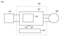
- the power conversion system shown in FIG. 12 is composed of a power source 100, a power conversion device 200, and a load 300.
- the power source 100 is a DC power source and supplies DC power to the power conversion device 200.
- the power source 100 is not particularly limited, and may be composed of, for example, a DC system, a solar cell, or a storage battery, or may be composed of a rectifier circuit or an AC/DC converter connected to an AC system.
- the power source 100 may be composed of a DC/DC converter that converts the DC power output from the DC system into a specified power.
- the power conversion device 200 is a three-phase inverter connected between the power source 100 and the load 300, converts the DC power supplied from the power source 100 into AC power, and supplies the AC power to the load 300. As shown in FIG. 12, the power conversion device 200 includes a main conversion circuit 201 that converts the DC power into AC power and outputs it, and a control circuit 203 that outputs a control signal to the main conversion circuit 201 to control the main conversion circuit 201.
- the load 300 is a three-phase motor that is driven by AC power supplied from the power conversion device 200.
- the load 300 is not limited to a specific use, but is a motor mounted on various electrical devices, and is used, for example, as a motor for a hybrid vehicle, an electric vehicle, a railroad car, an elevator, or an air conditioning device.
- the power conversion device 200 will be described in detail below.
- the main conversion circuit 201 includes a switching element (not shown) and a free wheel diode (not shown).
- the switching element switches the voltage supplied from the power source 100, so that the main conversion circuit 201 converts the DC power supplied from the power source 100 into AC power and supplies it to the load 300.
- the main conversion circuit 201 of this embodiment is a two-level three-phase full bridge circuit that can be composed of six switching elements and six free wheel diodes connected in reverse parallel to each switching element.
- each switching element and each free wheel diode of the main conversion circuit 201 the semiconductor elements 30 and 31 included in any of the power modules 1 of the above-mentioned embodiments 1 to 3 and their modifications can be applied.
- the power module 202 constituting the main conversion circuit 201 any of the power modules 1 of the above-mentioned embodiments 1 to 3 and their modifications can be applied.
- the six switching elements are connected in series in pairs to form upper and lower arms, and each upper and lower arm constitutes one phase (U phase, V phase, and W phase) of the full bridge circuit.
- the output terminals of each upper and lower arm, i.e., the three output terminals of the main conversion circuit 201 are connected to the load 300.
- the main conversion circuit 201 also includes a drive circuit (not shown) that drives each switching element.
- the drive circuit may be built into the power module 202 or may be provided outside the power module 202.
- the drive circuit generates drive signals that drive the switching elements included in the main conversion circuit 201 and supplies the drive signals to the control electrodes of the switching elements of the main conversion circuit 201.
- the drive circuit outputs a drive signal that switches the switching element to an on state and a drive signal that switches the switching element to an off state to the control electrodes of each switching element.
- the control circuit 203 controls the switching elements of the main conversion circuit 201 so that power is supplied to the load 300. Specifically, it calculates the time (on time) that each switching element of the main conversion circuit 201 should be in the on state based on the power to be supplied to the load 300.
- the main conversion circuit 201 can be controlled by PWM control, which modulates the on time of the switching elements according to the voltage to be output to the load 300. Then, it outputs a control command (control signal) to a drive circuit provided in the main conversion circuit 201 so that an on signal is output to the switching element that should be in the on state at each point in time, and an off signal is output to the switching element that should be in the off state.
- the drive circuit outputs an on signal or an off signal as a drive signal to the control electrode of each switching element according to this control signal.
- any of the power modules 1 of the first to third embodiments and their modifications is applied as the power module 202 included in the main conversion circuit 201. Therefore, the power conversion device 200 of this embodiment has improved reliability.
- a two-level power conversion device is used, but it may be a three-level power conversion device or a multi-level power conversion device.
- the present disclosure may be applied to a single-phase inverter.
- the present disclosure may be applied to a DC/DC converter or an AC/DC converter.
- the power conversion device to which this disclosure is applied is not limited to cases where the load is an electric motor, but may be incorporated, for example, into a power supply device for an electric discharge machine or a laser processing machine, or into a power supply device for an induction heating cooker or a contactless power supply system.
- a power conversion device to which this disclosure is applied may also be used as a power conditioner for a solar power generation system or a power storage system, etc.
Landscapes
- Inverter Devices (AREA)
Priority Applications (4)
| Application Number | Priority Date | Filing Date | Title |
|---|---|---|---|
| DE112023006608.6T DE112023006608T5 (de) | 2023-07-03 | 2023-07-03 | Leistungsmodul und Verfahren zum Herstellen desselben sowie Stromrichtereinrichtung |
| CN202380099867.4A CN121444663A (zh) | 2023-07-03 | 2023-07-03 | 功率模块及其制造方法以及电力变换装置 |
| PCT/JP2023/024607 WO2025009015A1 (ja) | 2023-07-03 | 2023-07-03 | パワーモジュール及びその製造方法並びに電力変換装置 |
| JP2025530815A JPWO2025009015A1 (https=) | 2023-07-03 | 2023-07-03 |
Applications Claiming Priority (1)
| Application Number | Priority Date | Filing Date | Title |
|---|---|---|---|
| PCT/JP2023/024607 WO2025009015A1 (ja) | 2023-07-03 | 2023-07-03 | パワーモジュール及びその製造方法並びに電力変換装置 |
Publications (1)
| Publication Number | Publication Date |
|---|---|
| WO2025009015A1 true WO2025009015A1 (ja) | 2025-01-09 |
Family
ID=94171879
Family Applications (1)
| Application Number | Title | Priority Date | Filing Date |
|---|---|---|---|
| PCT/JP2023/024607 Pending WO2025009015A1 (ja) | 2023-07-03 | 2023-07-03 | パワーモジュール及びその製造方法並びに電力変換装置 |
Country Status (4)
| Country | Link |
|---|---|
| JP (1) | JPWO2025009015A1 (https=) |
| CN (1) | CN121444663A (https=) |
| DE (1) | DE112023006608T5 (https=) |
| WO (1) | WO2025009015A1 (https=) |
Citations (4)
| Publication number | Priority date | Publication date | Assignee | Title |
|---|---|---|---|---|
| JP2010093287A (ja) * | 2009-12-17 | 2010-04-22 | Mitsubishi Electric Corp | パワー半導体モジュール |
| JP2011114137A (ja) * | 2009-11-26 | 2011-06-09 | Mitsubishi Electric Corp | 電力用半導体装置 |
| JP2020178003A (ja) * | 2019-04-17 | 2020-10-29 | 三菱電機株式会社 | パワー半導体モジュールおよびパワー半導体モジュールの製造方法 |
| JP2023008226A (ja) * | 2021-07-05 | 2023-01-19 | 三菱電機株式会社 | 半導体装置および半導体装置の製造方法 |
Family Cites Families (1)
| Publication number | Priority date | Publication date | Assignee | Title |
|---|---|---|---|---|
| JP3469840B2 (ja) | 2000-02-22 | 2003-11-25 | 株式会社三社電機製作所 | 半導体装置 |
-
2023
- 2023-07-03 JP JP2025530815A patent/JPWO2025009015A1/ja active Pending
- 2023-07-03 CN CN202380099867.4A patent/CN121444663A/zh active Pending
- 2023-07-03 WO PCT/JP2023/024607 patent/WO2025009015A1/ja active Pending
- 2023-07-03 DE DE112023006608.6T patent/DE112023006608T5/de active Pending
Patent Citations (4)
| Publication number | Priority date | Publication date | Assignee | Title |
|---|---|---|---|---|
| JP2011114137A (ja) * | 2009-11-26 | 2011-06-09 | Mitsubishi Electric Corp | 電力用半導体装置 |
| JP2010093287A (ja) * | 2009-12-17 | 2010-04-22 | Mitsubishi Electric Corp | パワー半導体モジュール |
| JP2020178003A (ja) * | 2019-04-17 | 2020-10-29 | 三菱電機株式会社 | パワー半導体モジュールおよびパワー半導体モジュールの製造方法 |
| JP2023008226A (ja) * | 2021-07-05 | 2023-01-19 | 三菱電機株式会社 | 半導体装置および半導体装置の製造方法 |
Also Published As
| Publication number | Publication date |
|---|---|
| DE112023006608T5 (de) | 2026-04-23 |
| JPWO2025009015A1 (https=) | 2025-01-09 |
| CN121444663A (zh) | 2026-01-30 |
Similar Documents
| Publication | Publication Date | Title |
|---|---|---|
| JP6881238B2 (ja) | 半導体モジュール、その製造方法及び電力変換装置 | |
| JP6826665B2 (ja) | 半導体装置、半導体装置の製造方法及び電力変換装置 | |
| JP6952889B2 (ja) | パワー半導体モジュール及びその製造方法並びに電力変換装置 | |
| CN113646876B (zh) | 功率半导体模块以及电力变换装置 | |
| JP6927437B1 (ja) | パワーモジュールおよび電力変換装置 | |
| CN110178219A (zh) | 半导体装置以及电力变换装置 | |
| JP7561677B2 (ja) | 電力半導体装置、電力半導体装置の製造方法及び電力変換装置 | |
| CN111052325B (zh) | 半导体模块以及电力转换装置 | |
| US12074132B2 (en) | Semiconductor device, power converter, and method of manufacturing semiconductor device | |
| CN111788694B (zh) | 半导体元件、半导体装置、电力变换装置以及半导体元件的制造方法 | |
| WO2021157024A1 (ja) | 半導体モジュール及び電力変換装置 | |
| CN113841237B (zh) | 功率半导体模块以及电力变换装置 | |
| WO2025009015A1 (ja) | パワーモジュール及びその製造方法並びに電力変換装置 | |
| WO2018189948A1 (ja) | 半導体モジュール、半導体モジュールの製造方法および電力変換装置 | |
| JP7334369B1 (ja) | パワーモジュール及び電力変換装置 | |
| WO2022049660A1 (ja) | 半導体装置、電力変換装置、および移動体 | |
| JP2022029886A (ja) | 半導体装置、半導体装置の製造方法及び電力変換装置 | |
| JP7438466B1 (ja) | 半導体装置及びその製造方法並びに電力変換装置 | |
| JP7651289B2 (ja) | パワー半導体モジュール及びその製造方法並びに電力変換装置 | |
| JP7686143B2 (ja) | 半導体装置、電力変換装置および半導体装置の製造方法 | |
| WO2025062638A1 (ja) | パワーモジュール、電子装置及び電力変換装置 | |
| JP2024165654A (ja) | 半導体装置、電力変換装置および半導体装置の製造方法 | |
| WO2025099830A1 (ja) | パワー半導体装置、パワーモジュール及び電力変換装置 | |
| WO2024171273A1 (ja) | 半導体モジュール及び電力変換装置 | |
| WO2023073752A1 (ja) | 半導体装置、電力変換装置、および半導体装置の製造方法 |
Legal Events
| Date | Code | Title | Description |
|---|---|---|---|
| 121 | Ep: the epo has been informed by wipo that ep was designated in this application |
Ref document number: 23944269 Country of ref document: EP Kind code of ref document: A1 |
|
| ENP | Entry into the national phase |
Ref document number: 2025530815 Country of ref document: JP Kind code of ref document: A |
|
| WWE | Wipo information: entry into national phase |
Ref document number: 2025530815 Country of ref document: JP |
|
| WWE | Wipo information: entry into national phase |
Ref document number: 112023006608 Country of ref document: DE |