WO2025004928A1 - アンテナ素子、アンテナアレイおよびアンテナモジュール - Google Patents
アンテナ素子、アンテナアレイおよびアンテナモジュール Download PDFInfo
- Publication number
- WO2025004928A1 WO2025004928A1 PCT/JP2024/022207 JP2024022207W WO2025004928A1 WO 2025004928 A1 WO2025004928 A1 WO 2025004928A1 JP 2024022207 W JP2024022207 W JP 2024022207W WO 2025004928 A1 WO2025004928 A1 WO 2025004928A1
- Authority
- WO
- WIPO (PCT)
- Prior art keywords
- conductor layer
- antenna
- antenna element
- layer
- interlayer connection
- Prior art date
- Legal status (The legal status is an assumption and is not a legal conclusion. Google has not performed a legal analysis and makes no representation as to the accuracy of the status listed.)
- Ceased
Links
Images




















Classifications
-
- H—ELECTRICITY
- H01—ELECTRIC ELEMENTS
- H01Q—ANTENNAS, i.e. RADIO AERIALS
- H01Q1/00—Details of, or arrangements associated with, antennas
- H01Q1/52—Means for reducing coupling between antennas; Means for reducing coupling between an antenna and another structure
-
- H—ELECTRICITY
- H01—ELECTRIC ELEMENTS
- H01Q—ANTENNAS, i.e. RADIO AERIALS
- H01Q21/00—Antenna arrays or systems
- H01Q21/06—Arrays of individually energised antenna units similarly polarised and spaced apart
-
- H—ELECTRICITY
- H01—ELECTRIC ELEMENTS
- H01Q—ANTENNAS, i.e. RADIO AERIALS
- H01Q9/00—Electrically-short antennas having dimensions not more than twice the operating wavelength and consisting of conductive active radiating elements
- H01Q9/04—Resonant antennas
- H01Q9/30—Resonant antennas with feed to end of elongated active element, e.g. unipole
- H01Q9/42—Resonant antennas with feed to end of elongated active element, e.g. unipole with folded element, the folded parts being spaced apart a small fraction of the operating wavelength
Definitions
- the short wavelength allows the elements to be miniaturized, so pattern antennas formed from conductive materials on electronic substrates are common.
- the patch antenna which is a planar antenna, is widely known as the antenna structure that is highly mass-producible and has been most widely used as a directional antenna (see Patent Document 1, for example).
- the objective of this technology is to provide an antenna element, antenna array, and antenna module that can achieve compact size and broadband with a simple structure.
- An antenna element includes a first conductor layer having a planar element shape, a second conductor layer, a dielectric layer, a first interlayer connection portion, and a second interlayer connection portion.
- the second conductor layer is connected to a ground potential.
- the dielectric layer is provided between the first conductor layer and the second conductor layer.
- the first interlayer connection passes through the dielectric layer and connects the first conductor layer to a power supply.
- the second interlayer connection portion penetrates the dielectric layer and connects between the first conductor layer and the second conductor layer.
- the first conductor layer functions as a radiating element
- the second conductor layer functions as a ground conductor plate
- the first interlayer connection, the first conductor layer, and the second interlayer connection form a loop antenna.
- the first conductor layer is typically formed with an area smaller than that of the second conductor layer. This makes it possible to achieve stable resonance in the desired frequency band.
- the loop length formed by the first interlayer connection, the first conductor layer, and the second interlayer connection may be equal to or less than one wavelength of the radio wave being used, for example, a half wavelength. This allows the antenna element to be further miniaturized.
- the planar shape of the first conductor layer may be a rectangle having long and short sides.
- the first conductor layer may have a first region to which the first interlayer connection portion is connected and a second region to which the second interlayer connection portion is connected, and the first region and the second region may be disposed away from the periphery of the first conductor layer. This can widen the directionality of radio waves.
- the first region and the second region may be arranged in a direction parallel to the long side, or in a direction intersecting the direction parallel to the long side.
- the dielectric layer may be a dielectric substrate made of a dielectric material
- the first conductor layer may be a metal layer formed on a first main surface of the dielectric substrate
- the second conductor layer may be a metal layer formed on a second main surface of the dielectric substrate opposite the first main surface.
- the second conductor layer may have an opening formed with a larger opening diameter than the first interlayer connection portion. This simplifies the electrical insulation structure between the first interlayer connection portion and the second conductor layer.
- the first interlayer connection and the second interlayer connection may be through-hole plating or buried vias provided in the dielectric layer.
- 13 is a simulation result showing radiation characteristics in the azimuth plane at 60 GHz of the antenna element according to Comparative Example 1.
- 11 is a simulation result showing radiation characteristics in the elevation plane at 60 GHz of the antenna element according to Comparative Example 1.
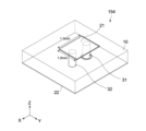
- FIG. 11 is a see-through perspective view of an antenna element according to Comparative Example 2.
- FIG. 11 is a side view of an antenna element according to Comparative Example 2.
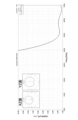
- 13 is a simulation result showing an example of a voltage standing wave ratio of an antenna element according to Comparative Example 2.
- 13 is a simulation result showing radiation characteristics in the azimuth plane at 60 GHz of the antenna element according to Comparative Example 2.
- 13 is a simulation result showing radiation characteristics in the elevation plane at 60 GHz of the antenna element according to Comparative Example 2.
- FIG. 7 is a simulation result comparing antenna characteristics and directivity between the antenna element shown in FIG. 1 and the antenna element of Comparative Example 1 shown in FIG. 6 .
- FIG. 11 is a see-through perspective view of an antenna module according to a second embodiment of the present technology.
- FIG. 2 is a plan view of the antenna module.
- FIG. 2 is a block diagram showing a circuit configuration of the antenna module.
- 18 is a perspective view similar to FIG. 17, showing the configuration of the antenna module to which no isolation processing has been applied.
- FIG. 6 is a simulation result showing the isolation characteristics of one receiving antenna with respect to a transmitting antenna in the above antenna module.
- 11 is a simulation result showing isolation characteristics of a receiving antenna with respect to a transmitting antenna in the above antenna module.
- FIG. 4 is a perspective view showing another configuration example of the antenna element shown in FIG. Simulation results showing the voltage standing wave ratio (VSWR) characteristics of the antenna element shown in Figure 36 and the radiation characteristics in the azimuth and elevation planes at 60 GHz. 1.
- FIG. 4 is a perspective view showing another configuration example of the antenna element shown in FIG. 39 is a simulation result showing the voltage standing wave ratio (VSWR) characteristic of the antenna element shown in FIG. 38 and the radiation characteristic in the azimuth plane and the elevation plane at 60 GHz.
- 13A and 13B are diagrams illustrating an example of an antenna module corresponding to a second embodiment.
- FIG. 41 is a diagram showing the isolation characteristics of the antenna module shown in FIG. 40.
- FIG. 13 is a see-through perspective view of an antenna module according to a fourth embodiment.
- FIG. 13 is a plan view of an antenna module according to a fourth embodiment.
- FIG. 13 is a diagram showing the isolation characteristics of the antenna module according to the fourth embodiment.
- FIG. 13 is a see-through perspective view of an antenna module according to a modified example of the fourth embodiment.
- FIG. 13 is a diagram showing the isolation characteristics of an antenna module according to a modified example of the fourth embodiment.
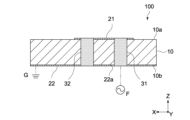
- Fig. 1 is a transparent perspective view of an antenna element 100 according to a first embodiment of the present technology
- Fig. 2 is a side cross-sectional view thereof.
- the X-axis, the Y-axis, and the Z-axis indicate three axial directions perpendicular to each other, and correspond to the vertical direction (front-rear direction), the horizontal direction (width direction), and the thickness direction (height direction) of the antenna element 100, respectively.
- the antenna element 100 of this embodiment is configured as a millimeter wave antenna for transmission, reception, or transmission and reception.
- the antenna element 100 includes a dielectric layer 10, a first conductor layer 21, a second conductor layer 22, a first interlayer connection portion 31, and a second interlayer connection portion 32.
- the antenna element 100 is configured by a dielectric multilayer substrate (double-sided wiring substrate).
- the dielectric layer 10 is provided between the first conductor layer 21 and the second conductor layer 22.
- the dielectric layer 10 is a dielectric substrate having rigidity, and corresponds to the insulating layer constituting the dielectric multilayer substrate.
- the dielectric layer 10 has a rectangular planar shape, and is formed with a vertical (X-axis direction) and horizontal (Y-axis direction) length of, for example, about 5 mm.
- the thickness (Z-axis direction) of the dielectric layer 10 is set according to the dielectric constant of the dielectric material constituting the dielectric layer 10 and the wavelength of the radio waves used, and is, for example, 0.65 mm in this embodiment that uses radio waves in the 60 GHz band.
- the dielectric material constituting the dielectric layer 10 may be, for example, insulating organic materials such as FR4, BT resin, and polytetrafluoroethylene, and insulating inorganic materials such as ceramics.
- the dielectric constant of the dielectric layer 10 is not particularly limited, and can be set arbitrarily according to the frequency of the radio waves transmitted or received by the antenna element 100. For example, when used to transmit and receive electromagnetic waves in the 60 GHz band, a material with a dielectric constant of, for example, 3.6 is used for the dielectric substrate 10.
- the first conductor layer 21 corresponds to a conductor layer formed on one surface side of the dielectric multilayer substrate, and in this embodiment is a metal layer formed on the first main surface 10a (the upper surface in Figures 1 and 2) of the dielectric layer 10.
- the first conductor layer 21 is configured as a radiating element of the antenna element 100.
- the first conductor layer 21 is formed with an area smaller than that of the second conductor layer 22, and is formed into a planar pattern having a planar element shape, for example, a rectangle.
- the planar element shape refers to the planar shape (patch shape) of a conductor portion that forms a radiating element such as a patch antenna.
- the size (length of each side) of the first conductor layer 21 is not particularly limited and can be set arbitrarily depending on the frequency band of the radio waves used. In this embodiment, the length of the long side 21L along the X-axis direction is approximately 1.6 mm, and the length of the short side 21S along the Y-axis direction is approximately 1.0 mm.
- the planar shape of the first conductor layer 21 is not limited to a rectangle, but may be a polygon other than a rectangle, a circle, an ellipse, or a combination of these. In addition, at least a part of the rectangle (e.g., a side or a vertex) may be deformed into any shape.
- the second conductor layer 22 corresponds to a conductor layer formed on the other surface side of the dielectric multilayer substrate, and in this embodiment is a metal layer formed on the second main surface 10b (the bottom surface in Figures 1 and 2) opposite the first main surface 10a of the dielectric layer 10.
- the second conductor layer 22 is configured as a ground conductor plate for the antenna element 100. By being electrically connected to the ground potential G, the second conductor layer 22 is formed over the entire back surface 10b of the dielectric layer 10, but is of course not limited to this.
- the metals constituting the first conductor layer 21 and the second conductor layer 22 are not particularly limited, and examples include copper and aluminum.
- the thicknesses of the first conductor layer 21 and the second conductor layer 22 are not particularly limited, and they may be formed to the same thickness or different thicknesses.
- the first interlayer connection 31 penetrates the dielectric layer 10 in its thickness direction (Z-axis direction) and connects the first conductor layer 21 to the power supply F.
- the first interlayer connection 31 is a cylindrical conductor electrically connected to the first conductor layer 21, and in this embodiment is formed by through-hole plating provided in the dielectric layer 10 or a buried via filled with a conductive material.
- the second conductor layer 22 has an opening 22a formed with an opening diameter larger than the outer diameter of the first interlayer connection 31.
- the first interlayer connection 31 is electrically insulated from the second conductor layer 22 by being accommodated in the opening 22a without contacting the peripheral portion of the opening 22a.
- the annular region between the opening 22a and the first interlayer connection 31 may be filled with the same material as the dielectric layer 10 or a different dielectric material.
- the second interlayer connection portion 32 penetrates the dielectric layer 10 in its thickness direction (Z-axis direction) and electrically connects between the first conductor layer 21 and the second conductor layer 22.
- the second interlayer connection portion 32 is a cylindrical conductor like the first interlayer connection portion 31, and in this embodiment is formed by through-hole plating provided in the dielectric layer 10 or by an embedded via filled with a conductive material.
- the second interlayer connection portion 32 is formed with the same diameter and height as the first interlayer connection portion 31.
- the first interlayer connection portion 31 and the second interlayer connection portion 32 are connected perpendicularly to the first conductor layer 21. Therefore, the length (height) of the first interlayer connection portion 31 and the second interlayer connection portion 32 corresponds to the thickness (0.65 mm) of the dielectric layer 10.
- the first conductor layer 21 has a first region 211 to which the first interlayer connection portion 31 is connected, and a second region 212 to which the second interlayer connection portion 32 is connected.
- the first region 211 and the second region 212 are both located within the plane of the first conductor layer 21 and spaced apart from the peripheral portion of the first conductor layer 21.
- first region 211 and the second region 212 are arranged in a direction parallel to the long side 21L (X-axis direction) at positions symmetrical with respect to the center of the first conductor layer 21. This is not limiting, and the first region 211 and the second region 212 may be arranged in a direction intersecting the direction parallel to the long side 21L (X-axis direction) as described later (see FIG. 38).
- the antenna element 100 of this embodiment configured as described above is configured as a loop antenna having an axis parallel to the width direction (Y-axis direction) by the first conductor layer 21, the first interlayer connection part 31, and the second interlayer connection part 32.
- the length of each side (long side 21L, short side 21S) of the first conductor layer 21 is set so that the frequency band of the radio waves used is 60 GHz (e.g., 57 GHz to 64 GHz).
- the first conductor layer 21 is formed in a planar element shape with a length and width greater than the axial diameter and arrangement spacing of the interlayer connections 31, 32, the current density is concentrated on the periphery of the first conductor layer 21, and therefore the relative bandwidth can be increased by setting the length of each side of the first conductor layer 21.
- the loop length (effective length including wavelength shortening due to the dielectric constant of the dielectric layer 10) formed by the first interlayer connection 31, the second interlayer connection 32, and the first conductor layer 21 is set to be equal to or less than one wavelength of the radio wave being used, and more preferably, to a size equivalent to half the wavelength of the radio wave.
- the effective length is 2.477 mm, which is equivalent to a half wavelength of a 60 GHz radio wave.
- the antenna element 100 of this embodiment has multiple resonant frequencies including a resonant frequency corresponding to the loop length and a resonant frequency corresponding to the circumference length of the first conductor layer 21, so that the fractional bandwidth (value obtained by dividing the bandwidth by the center frequency) that can be covered by a single element can be increased.
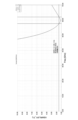
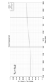
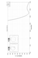
- Figure 3 shows a simulation result illustrating an example of the voltage standing wave ratio (VSWR) of the antenna element 100.
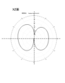
- Figure 4 shows a simulation result illustrating the radiation characteristics of the antenna element 100 in the azimuth plane (XZ plane) at 60 GHz
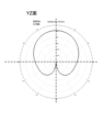
- Figure 5 shows a simulation result illustrating the radiation characteristics of the antenna element 100 in the elevation plane (YZ plane) at 60 GHz.
- the 0° direction (upward) corresponds to the top surface direction (+Z direction).
- the frequency band where the VSWR ratio was 1.5 or less was 59 GHz to 67 GHz, and the relative bandwidth was 12.7%. Also, as shown in Figures 4 and 5, a well-balanced directional characteristic was obtained over a wide range toward the top surface.
- this embodiment makes it possible to obtain antenna characteristics that resonate over a wide bandwidth, even with a single element structure.
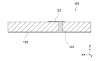
- Fig. 6 is a see-through perspective view of an antenna element 101 according to Comparative Example 1
- Fig. 7 is a side cross-sectional view of the antenna element 101.
- the antenna element 101 shows a typical structure of a back-feed type patch antenna.
- the antenna element 101 has a dielectric layer 110, a first conductor layer 121 as a radiating element formed on the surface of the dielectric layer 110, a second conductor layer 122 as a ground conductor plate formed on the back surface of the dielectric layer 110, and an interlayer connection portion 131 that penetrates the dielectric layer 110 and connects the first conductor layer 121 to a feed point.
- the interlayer connection portion 131 is electrically insulated from the second conductor layer 122.
- the shape of the first conductor layer 121 is a rectangle with long sides of 1.2 mm and short sides of 1.0 mm.
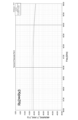
- Figure 8 shows a simulation result illustrating an example of the voltage standing wave ratio (VSWR) of the antenna element 101.
- Figure 9 shows a simulation result illustrating the radiation characteristics of the antenna element 101 in the azimuth plane (XZ plane) at 60 GHz
- Figure 10 shows a simulation result illustrating the radiation characteristics of the antenna element 101 in the elevation plane (YZ plane) at 60 GHz.
- the 0° direction (upward) corresponds to the top surface direction (+Z direction).
- the frequency band where the VSWR ratio is 1.5 or less is 57 GHz to 61 GHz, and the relative bandwidth is 6.7%.
- the relative bandwidth is 12.7% as described above (see FIG. 3), so the relative bandwidth can be increased by about two times compared to Comparative Example 1. This makes it possible to achieve a wider frequency band than the antenna element 101 of Comparative Example 1.
- the antenna directivity was almost the same as that of the antenna element 101 of Comparative Example 1 shown in Figures 9 and 10. This shows that this embodiment can expand the frequency band while providing antenna directivity equivalent to that of a patch antenna structure.
- FIG. 11 is a perspective view of an antenna element 102 according to Comparative Example 2
- Fig. 12 is a side view thereof.
- This antenna element 102 includes a loop-shaped antenna structure 123 formed perpendicular to a ground conductor plate 124. One end of the antenna structure is connected to a power feed point, and the other end is connected to the ground conductor plate 124.
- the loop length is set to a size equivalent to half the wavelength of a 60 GHz radio wave.
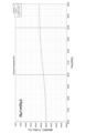
- Figure 13 shows a simulation result showing an example of the voltage standing wave ratio (VSWR) of the antenna element 102.
- Figure 14 shows a simulation result showing the radiation characteristics of the antenna element 102 in the azimuth plane (XZ plane) at 60 GHz
- Figure 15 shows a simulation result showing the radiation characteristics of the antenna element 102 in the elevation plane (YZ plane) at 60 GHz.
- the 0° direction (upward) corresponds to the top surface direction (+Z direction).
- the frequency band where the VSWR ratio is 1.5 or less is 58 GHz to 60 GHz, and the relative bandwidth is 6.6%.
- the relative bandwidth is 12.7% as described above (see FIG. 3), so the relative bandwidth can be increased by approximately two times compared to Comparative Example 2. This makes it possible to achieve a wider frequency band than the antenna element 101 of Comparative Example 1.
- the directivity has figure-8 characteristics like a dipole antenna, and is not suitable for use as a directional antenna toward the radiation surface (top surface) used in the millimeter wave region. Therefore, according to this embodiment, compared to a typical loop antenna structure, it is possible to achieve a wide frequency band while achieving well-balanced directional characteristics over a wide range toward the top surface.
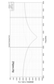
- Figure 16 shows the results of a simulation comparing the antenna characteristics and directivity of the antenna element 100 of this embodiment and the antenna element 101 of Comparative Example 1.
- each element was formed to the same size with a resonant frequency of 60 GHz, and the antenna characteristics and directivity from 50 to 65 GHz were measured at 5 GHz intervals.
- the antenna element 100 of this embodiment has a directional characteristic similar to that of the antenna element 101 of Comparative Example 1.
- the antenna gain in the top surface direction in the frequency range of 55 GHz to 65 GHz exceeds that of Comparative Example 1.
- methods such as making it into an array shape requiring multiple antenna elements or increasing the number of layers in a laminated substrate and adding reflection/broadening patterns in between have been used.
- broadening the bandwidth can be achieved using an inexpensive and simple method.
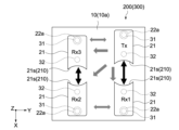
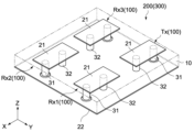
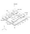
- Fig. 17 is a see-through perspective view of an antenna module 300 according to a second embodiment of the present technology
- Fig. 18 is a plan view thereof
- Fig. 19 is a block diagram showing a circuit configuration of the antenna module 300.
- parts corresponding to those in the above-described first embodiment are given the same reference numerals, and description thereof will be omitted.
- the antenna module 300 of this embodiment includes an antenna array 200 and a signal processing circuit 301 ( Figure 19).
- the antenna array 200 and the signal processing circuit 301 are formed or mounted on a common dielectric multilayer substrate 1.
- the antenna array 200 has a plurality of antenna elements 100.
- the plurality of antenna elements 100 includes one transmitting antenna Tx and three receiving antennas Rx1, Rx2, and Rx3.
- Each antenna element 100 has the same configuration, and is configured similarly to the antenna element described in the first embodiment.
- the number of transmitting antennas is not limited to one, and may be two or more.
- the number of receiving antennas is not limited to three, and may be two or four or more.
- each antenna element 100 is arranged independently on the first main surface 10a of the dielectric layer 10.
- Each first conductor layer 21 is formed into a similar planar element shape, and in this embodiment is formed into a roughly rectangular shape with a long side in the X-axis direction and a short side in the Y-axis direction.
- These antenna elements 100 are arranged in a matrix along the X-axis and Y-axis directions on the first main surface 10a of the dielectric layer 10, as shown in FIG. 18.
- the second conductor layer 22 of each antenna element 100 is formed of a common conductor layer connected to ground potential.
- An opening 22a is provided in the second conductor layer 22 in the region where the first interlayer connection portion 31 of each antenna element 100 is formed, thereby electrically insulating the second conductor layer 22 from each first interlayer connection portion 31.
- the first interlayer connection portion 31 of each antenna element 100 is connected to the signal processing circuit 301 via a signal transmission line (not shown) formed on the second main surface 10b of the dielectric layer 10.
- a signal transmission line As the signal transmission line, various signal lines such as a microstrip line, a strip line, and a coplanar waveguide line can be used.
- the signal processing circuit 301 is a millimeter wave radar IC that generates a millimeter wave signal to be transmitted to the transmitting antenna Tx and processes the millimeter wave signals received by the receiving antennas Rx1 to Rx3 to calculate the angle of arrival, and corresponds to a power supply unit.
- the dielectric multilayer substrate 1 further includes a regulator 302 that adjusts the voltage supplied to the signal processing circuit 301, a memory 303 that stores driving parameters for the signal processing circuit 301, and a connector 304 that electrically connects the signal processing circuit, the regulator 302, and the memory 303 to an external device (not shown), as shown in FIG.
- the antenna module 300 of this embodiment is configured as a MIMO (Multi-Input Multi-Output) radar antenna. According to this embodiment, transmitting and receiving antennas are mounted on the same substrate, so that it is possible to obtain the same effects as the first embodiment described above, while also making it possible to reduce the size and thickness of the antenna device.
- MIMO Multi-Input Multi-Output
- the first conductor layer 21 of each antenna element 100 constituting the antenna array 200 has a rectangular planar shape with long sides parallel to the X-axis direction and short sides parallel to the Y-axis direction. Therefore, when the antenna elements 100 are arranged on the first main surface 10a of the square-shaped dielectric layer 10, the interval between adjacent antenna elements 100 in the X-axis direction is smaller than the interval between adjacent antenna elements 100 in the Y-axis direction.
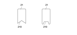
- a cutout portion 210 that partially expands the distance between the two first conductor layers 21 is provided on the opposing short sides 21s of the two first conductor layers 21 arranged in the X-axis direction. This makes it possible to improve the isolation characteristics between two antenna elements 100 adjacent in the X-axis direction (between the transmitting antenna Tx and the receiving antenna Rx1, and between the two receiving antennas Rx2 and Rx3) compared to an antenna array 200 that does not have a cutout portion 210, as shown in FIG. 20, for example.
- the shape of the cutout portion 210 is not particularly limited, and in this embodiment, it is formed in an arc shape. Alternatively, as shown in FIG. 27, the cutout portion 210 may be formed in a triangular shape, a rectangular shape, or a trapezoidal shape.
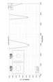
- Figure 21 shows the results of a simulation showing the isolation characteristics of receiving antenna Rx1 relative to transmitting antenna Tx.
- the solid line in the figure shows the characteristics when there is a cutout 210 (hereinafter also referred to as with isolation processing), and the dashed line shows the characteristics when there is no cutout 210 (hereinafter also referred to as without isolation processing).
- With isolation processing an improvement of approximately 1 dB is observed compared to without isolation processing.
- Figure 22 shows the results of a simulation showing the isolation characteristics of the receiving antenna Rx2 with respect to the transmitting antenna Tx.
- the solid line in the figure shows the characteristics with isolation processing, and the dashed line shows the characteristics without isolation processing.
- no significant difference was observed between the cases with and without isolation processing. This is thought to be because the transmitting antenna Tx and receiving antenna Rx2 are diagonally positioned with respect to each other, and there is a large physical distance between them.
- Figure 23 shows the results of a simulation showing the isolation characteristics of the receiving antenna Rx3 relative to the transmitting antenna Tx.
- the solid line in the figure shows the characteristics with isolation processing
- the dashed line shows the characteristics without isolation processing.
- With isolation processing a significant improvement is seen in the 60 GHz to 64 GHz band compared to without isolation processing. This is thought to be because, since the long sides of the first conductor layer 21 of the transmitting antenna Tx and the receiving antenna Rx3 face each other, there is no effect from the formation of the notch 210, but because the current density is high at the periphery of the first conductor layer 21, the shape effect of the notch 210 provides a filter-like function at a specific frequency.
- Figure 24 shows the simulation results showing the isolation characteristics between receiving antennas Rx2 and Rx3.
- the solid line in the figure shows the characteristics when isolation processing is applied, and the dashed line shows the characteristics when isolation processing is not applied.
- an improvement of approximately 2 dB is observed compared to when isolation processing is not applied.
- Figure 25 shows the results of a simulation showing the isolation characteristics between receiving antennas Rx1 and Rx3.
- the solid line shows the characteristics when isolation processing is applied
- the dashed line shows the characteristics when isolation processing is not applied.
- no significant difference was observed between the cases with and without isolation processing. This is thought to be because receiving antennas Rx1 and Rx3 are diagonally opposite each other, and the physical distance between them is large.
- Figure 26 shows the results of a simulation showing the isolation characteristics between receiving antennas Rx1 and Rx2.
- the solid line in the figure shows the characteristics when isolation processing is applied, and the dashed line shows the characteristics when isolation processing is not applied.
- the shape effect of the cutout portion 210 provides a filter-like function at a specific frequency.
- the antenna element 151 shown in FIG. 28 differs from the antenna element 100 shown in FIG. 1 in that the first conductor layer 21 serving as the radiating element is formed with the same area as the second conductor layer 22 serving as the ground conductor plate.
- the length of each side of the first conductor layer 21 and the second conductor layer 22 is set to 3 mm.
- Figure 29 shows the results of a simulation showing the voltage standing wave ratio (VSWR) characteristics of the antenna element 151 and the radiation characteristics in the azimuth plane (XZ plane) and elevation plane (YZ plane) at 60 GHz.
- VSWR voltage standing wave ratio
- the area of the first conductor layer 21 is too large, which changes the resonance state and makes it difficult to use as an antenna for the 60 GHz band.
- the first conductor layer 21 must be formed with an area at least smaller than that of the second conductor layer 22, for example, and it is preferable to optimize the circuit length of the first conductor layer 21 according to the band being used.
- Figure 31 shows the simulation results showing the voltage standing wave ratio (VSWR) characteristics of the antenna element 152 and the radiation characteristics in the azimuth plane (XZ plane) and elevation plane (YZ plane) at 60 GHz. As shown in the figure, resonance occurs in the 60 GHz band, but the radiation characteristics of the antenna remain directional like a loop antenna.
- VSWR voltage standing wave ratio
- the antenna element 153 shown in FIG. 32 differs from the antenna element 152 shown in FIG. 30 in that, when viewed from the Z-axis direction, the antenna element 153 is formed in a band shape with the outer periphery of the first interlayer connection portion 31 (first region 211) and the second interlayer connection portion 32 (second region 212) located inside the peripheral portion (long side and short side) of the first conductor layer 21 as a radiating element.
- the length of the short side of the first conductor layer 21 is 0.5 mm
- the length of the long side is 1.3 mm.
- Figure 33 shows the simulation results showing the voltage standing wave ratio (VSWR) characteristics of antenna element 153 and the radiation characteristics in the azimuth plane (XZ plane) and elevation plane (YZ plane) at 60 GHz. As shown in the figure, the band begins to widen around the 60 GHz band, and as an antenna, the radiation characteristics toward the ceiling become larger.
- VSWR voltage standing wave ratio
- Figure 35 shows the simulation results showing the voltage standing wave ratio (VSWR) characteristics of the antenna element 154 and the radiation characteristics in the azimuth plane (XZ plane) and elevation plane (YZ plane) at 60 GHz. As shown in the figure, it can be seen that the band is further expanded and the antenna radiation pattern is optimized in the direction of the ceiling.
- VSWR voltage standing wave ratio
- the antenna element 155 shown in FIG. 36 differs from the antenna element 154 shown in FIG. 34 in that the length of the short side of the first conductor layer 21 as the radiating element is 0.5 mm and the length of the long side is 1.6 mm.
- Figure 37 shows the simulation results showing the voltage standing wave ratio (VSWR) characteristics of antenna element 155 and the radiation characteristics in the azimuth plane (XZ plane) and elevation plane (YZ plane) at 60 GHz. As shown in the figure, multiple resonances are also generated in the Y-axis direction, widening the band, and the antenna radiation pattern becomes stronger toward the top surface.
- VSWR voltage standing wave ratio
- the two antenna elements 156 shown in FIG. 38 differ from the antenna element 100 shown in FIG. 1 in that the first interlayer connection portion 31 and the second interlayer connection portion 32 connected to the first conductor layer 21 as a radiating element are arranged in a direction intersecting the direction parallel to the long side (X-axis direction).
- the second interlayer connection portion 32 is arranged in a corner of the first conductor layer 21.
- Figure 39 shows simulation results showing the voltage standing wave ratio (VSWR) characteristics of antenna element 156 and the radiation characteristics in the azimuth plane (XZ plane) and elevation plane (YZ plane) at 60 GHz. As shown in the figure, simulation results similar to the VSWR characteristics ( Figure 3) and radiation characteristics ( Figures 4 and 5) of antenna element 100 shown in Figure 1 are obtained, so this configuration example can also achieve the same effects as the first embodiment.
- VSWR voltage standing wave ratio
- Figure 40 is a diagram showing an example of an antenna module 300 corresponding to the second embodiment described above.
- the antenna module 300 (antenna array 200) has multiple antenna elements 100, which include one transmitting antenna Tx and three receiving antennas Rx1, Rx2, and Rx3.
- the first conductor layers 21 of the transmitting antenna Tx and the receiving antennas Rx1, Rx2, and Rx each have a notch 210 on the short sides that face each other in the X-axis direction.
- the antenna module 300 has a rectangular shape in the planar direction, and in this example, the length in the X-axis direction is 5.0 mm, and the width in the Y-axis direction is 5.0 mm.
- the distance between the center position of receiving antenna Rx1 and the center position of receiving antenna Rx2, and the distance between the center position of receiving antenna Rx1 and the center position of receiving antenna Rx3, are 2.5 mm.
- the distance between the center position of receiving antenna Rx2 and the center position of receiving antenna Rx3, and the distance between the center position of receiving antenna Rx1 and the center position of receiving antenna Rx3, are 2.5 mm.
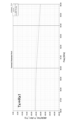
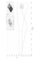
- FIG. 41 is a diagram showing the isolation characteristics of the antenna module 300 shown in FIG. 40.
- the horizontal axis shows the frequency [GHz] of the radio waves used in the antenna element 100
- the vertical axis shows the isolation characteristics [dB]. Note that a lower value [dB] on the vertical axis means a higher isolation characteristic.
- three graphs respectively show the isolation characteristics of the receiving antenna Rx1 relative to the transmitting antenna Tx (Tx ⁇ Rx1), the isolation characteristics of the receiving antenna Rx2 relative to the transmitting antenna Tx (Tx ⁇ Rx2), and the isolation characteristics of the receiving antenna Rx3 relative to the transmitting antenna Tx (Tx ⁇ Rx3).
- thermography format a map (in thermography format) is shown to visualize the effect of the transmitting antenna Tx on the receiving antennas Rx1, Rx2, and Rx3.
- the first conductor layer 21 has a notch 210, and therefore the isolation characteristics are improved compared to a configuration without the notch 210.
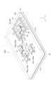
- FIG. 42 is a see-through perspective view of an antenna module 400 according to the fourth embodiment.
- FIG. 43 is a plan view of an antenna module 400 according to the fourth embodiment. In explaining this fourth embodiment, the differences from the second embodiment (and FIGS. 40 and 41) will be mainly explained.
- a notch 210 is provided in each of the first conductor layers 21 (similar to the second embodiment described above).
- a shielding layer 41 is provided to shield the electric field from the transmitting antenna Tx to the receiving antennas Rx1, Rx2, and Rx3.
- a third interlayer connection portion 42 is provided to connect the shielding layer 41 and the second conductor layer 22, and the shielding layer 41 is connected to the ground potential.
- the antenna module 400 (antenna array) has multiple antenna elements 100, which include one transmitting antenna Tx and three receiving antennas Rx1, Rx2, and Rx3.
- the first conductor layers 21 of the transmitting antenna Tx and the receiving antennas Rx1, Rx2, and Rx each have a notch 210 on the short sides that face each other in the X-axis direction.
- the antenna module 400 has a rectangular shape in the planar direction that is long in the X-axis direction.
- the length in the X-axis direction (direction parallel to the long side of the first conductor layer 21) is 12.5 mm
- the width in the Y-axis direction (direction parallel to the short side of the first conductor layer 21) is 7.5 mm (5 mm x 5 mm in Figure 40).
- the specific numerical values described in the fourth embodiment are merely examples and can be changed as appropriate.
- the distance between the center position of receiving antenna Rx1 and the center position of receiving antenna Rx2, and the distance between the center position of receiving antenna Rx1 and the center position of receiving antenna Rx3, are 2.5 mm.
- the distance between the center position of receiving antenna Rx2 and the center position of receiving antenna Rx3, and the distance between the center position of receiving antenna Rx1 and the center position of receiving antenna Rx3, are 2.5 mm.
- the distance D between the center position of the transmitting antenna Tx and the center positions of the three receiving antennas Rx1, Rx3, Rx3 is 5 mm.
- the center positions of the three receiving antennas Rx1, Rx3, Rx3 in the planar directions are the midpoint between the center positions of the receiving antenna Rx1 and the receiving antenna Rx2 in the Y-axis direction, and the midpoint between the center positions of the receiving antenna Rx2 and the receiving antenna Rx3 in the X-axis direction.
- the relative positional relationship of the three receiving antennas Rx1, Rx2, and Rx3 is the same as in the example shown in FIG. 40 (and in the second embodiment).
- the distance D between the center position of the transmitting antenna Tx and the center positions of the three receiving antennas Rx1, Rx3, and Rx3 is 2 mm in the example shown in FIG. 40, whereas in this example it is 5 mm, which is longer than the example shown in FIG. 40.
- the three receiving antennas Rx1, Rx2, R3 are moved in the X-axis direction away from the transmitting antenna Tx while the relative positional relationship between them remains fixed.
- the reason that the relative positional relationship between the three receiving antennas Rx1, Rx2, R3 is fixed is because the relative positional relationship between the three receiving antennas Rx1, Rx2, R3 is roughly determined due to the use of MIMO in this technology.
- the distance D in the XY directions (plane directions) between the center position of the transmitting antenna Tx and the center positions of the three receiving antennas Rx1, Rx3, and Rx3 is set to be equal to or greater than half the wavelength (1/2 ⁇ ) of the radio waves used.
- Experimental results have shown that by setting the distance D to a length equal to or greater than half the wavelength (1/2 ⁇ ), the isolation characteristics of the receiving antennas Rx1, Rx3, and Rx3 with respect to the transmitting antenna Tx are improved.
- the isolation characteristics of the receiving antennas Rx1, Rx3, and Rx3 relative to the transmitting antenna Tx will improve as the distance D is increased, but experimental results show that the tendency for improvement plateaus when the distance D exceeds a certain distance.
- the antenna module 400 becomes larger as the distance D is increased. If the antenna module 400 becomes larger, there is also the problem that transmission losses occur between the millimeter wave radar IC 301 and the receiving antenna Tx and the receiving antennas Rx1, Rx2, and Rx2, deteriorating the performance of the entire system.
- the distance D in the XY directions (planar directions) between the center position of the transmitting antenna Tx and the center positions of the three receiving antennas Rx1, Rx2, and Rx3 is set to 1.5 times (1.5 ⁇ ) the wavelength of the radio wave used. This allows the isolation characteristics to be appropriately improved without increasing the size of the antenna module 400.
- the shielding layer 41 is formed in a ring shape (and strip shape) on the surface 10a of the dielectric layer 10 so as to surround the first conductor layer 21 of the transmitting antenna Tx.
- the shielding layer 41 is in the shape of a rectangular ring, but this shape may be other shapes such as an elliptical ring.
- the shielding layer 41 is typically a metal layer formed on the surface 10a of the dielectric layer 10.
- Metal materials used for the shielding layer 41 include, for example, copper and aluminum, but the material is not particularly limited. The material may be the same as that of the first conductor layer 21 and the second conductor layer, or a different material may be used.
- the thickness of the shielding layer 41 is also not particularly limited, and may be the same thickness as that of the first conductor layer 21 and the second conductor layer 22, or may be a different thickness.
- the outer periphery of the shielding layer 41 is 3.5 mm x 3.5 mm (X-axis x Y-axis), and the width (band width) of the shielding layer 41 is 0.25 mm.
- the distance between the inner periphery of the shielding layer 41 and the long side of the first conductor layer 21 of the transmitting antenna Tx is 1 mm.
- the distance between the inner periphery of the shielding layer 41 and the short side of the first conductor layer 21 of the transmitting antenna Tx is 0.6 mm.
- the antenna module 400 also has a plurality of third interlayer connections 42.
- the third interlayer connections 42 penetrate the dielectric layer 10 in its thickness direction (Z-axis direction) and electrically connect between the shielding layer 41 and the second conductor layer 22.
- the third interlayer connections 42 are cylindrical conductors like the first interlayer connections 31 and the second interlayer connections 32, and are formed by through-hole plating provided in the dielectric layer 10 or embedded vias filled with a conductive material.
- the third interlayer connection part 42 is connected perpendicularly to the shielding layer 41 and the second conductor layer 22, so the length (height) of the third interlayer connection part 42 corresponds to the thickness (0.65 mm) of the dielectric layer 10.
- the diameter of the third interlayer connection part 42 is, for example, the same size as the width (band width) of the shielding layer 41.
- the diameter of the third interlayer connection part 42 may be the same as the diameter of the first interlayer connection part 31 and the second interlayer connection part 32, or may be a different diameter.
- the third interlayer connections 42 are arranged at a predetermined interval (0.8 mm) along the circumferential direction of the shielding layer 41.
- the third interlayer connections 42 are not provided around the entire circumference of the shielding layer 41, but are provided around a portion of the entire circumference of the shielding layer 41.
- the third interlayer connections 42 are provided at a location corresponding to one side along the Y-axis direction (one side between the transmitting antenna Tx and the receiving antenna Rx) and two sides along the X-axis direction among the four sides of the rectangle of the shielding layer 41.
- the third interlayer connections 42 may be provided around the entire circumference of the shielding layer 41.
- the shielding layer 41 is connected to the second conductor layer 22 via a plurality of third interlayer connections 42. Since the second conductor layer 22 is grounded, the shielding layer 41 is also at ground potential accordingly. In this way, by setting the shielding layer 41 at ground potential, it is possible to appropriately shield the electric field (radio waves) from the transmitting antenna Tx to the receiving antennas Rx1, Rx2, and Rx3.
- Figure 44 is a diagram showing the isolation characteristics of the antenna module 400.
- the horizontal axis shows the frequency [GHz] of the radio waves used in the antenna element 100
- the vertical axis shows the isolation characteristics [dB]. Note that a lower value [dB] on the vertical axis means a higher isolation characteristic.
- FIG. 44 three graphs respectively show the isolation characteristics of the receiving antenna Rx1 relative to the transmitting antenna Tx (Tx ⁇ Rx1), the isolation characteristics of the receiving antenna Rx2 relative to the transmitting antenna Tx (Tx ⁇ Rx2), and the isolation characteristics of the receiving antenna Rx3 relative to the transmitting antenna Tx (Tx ⁇ Rx3).
- thermography format a map (in thermography format) is shown to visualize the effect of the transmitting antenna Tx on the receiving antennas Rx1, Rx2, and Rx3.
- the value indicating the isolation characteristic is approximately 30 dB or less. In this way, by setting the value indicating the isolation characteristic to 30 dB or less, sufficient isolation characteristics can be obtained.
- the shielding layer 41 (metal layer) that shields the electric field from the transmitting antenna Tx to the receiving antennas Rx1, Rx2, and Rx3 is provided between the first conductor layer 21 of the transmitting antenna Tx and the first conductor layer 21 of the receiving antennas Rx1, Rx2, and Rx3 on the surface 10a of the dielectric layer 10. This can further improve the isolation characteristics of the receiving antennas Rx1, Rx2, and Rx3 with respect to the transmitting antenna Tx.
- the shielding layer 41 is formed in a ring shape on the surface 10a of the dielectric layer 10 so as to surround the first conductor layer 21 of the transmitting antenna Tx. This can further improve the isolation characteristics of the receiving antennas Rx1, Rx2, and Rx3 with respect to the transmitting antenna Tx.
- a third interlayer connection 42 is provided that penetrates the dielectric layer 10 and connects between the shielding layer 41 and the second conductor layer 22. This allows the shielding layer 41 to be at ground potential, and allows the electric field (radio waves) from the transmitting antenna Tx to the receiving antennas Rx1, Rx2, and Rx3 to be appropriately shielded.
- the third interlayer connection 42 is a through-hole plating or a buried via provided in the dielectric layer 10. This allows for an appropriate connection between the shielding layer 41 and the second conductor layer 22.
- the wavelength of the radio waves used is ⁇ and the distance in the planar direction between the center position of the transmitting antenna Tx and the center positions of the front receiving antennas Rx1, Rx2, and Rx3 is D, 0.5 ⁇ D ⁇ 1.5 ⁇ is satisfied.
- the distance D longer than half the wavelength (1/2 ⁇ )
- the isolation characteristics of the receiving antennas Rx1, Rx3, and Rx3 with respect to the transmitting antenna Tx can be further improved.
- the distance D 1.5 times (1.5 ⁇ ) or less the wavelength of the radio waves used the isolation characteristics can be appropriately improved without increasing the size of the antenna module 400.
- Fig. 45 is a see-through perspective view of an antenna module 500 according to a modified example of the fourth embodiment.
- the shielding portion 41 and the third interlayer connection portion 42 are omitted compared to the antenna module 400 shown in Fig. 42.
- the rest is the same as Fig. 42.
- the first conductor layers 21 of the transmitting antenna Tx and the receiving antennas Rx1, Rx2, and Rx each have a notch 210 on the short sides that face each other in the X-axis direction.
- the distance D between the center position of the transmitting antenna Tx and the center positions of the three receiving antennas Rx1, Rx3, and Rx3 is 5 mm. In other words, the distance D satisfies the condition 0.5 ⁇ D ⁇ 1.5 ⁇ .
- Figure 46 is a diagram showing the isolation characteristics of the antenna module 500.
- the horizontal axis shows the frequency [GHz] of the radio waves used in the antenna element 100
- the vertical axis shows the isolation characteristics [dB]. Note that a lower value [dB] on the vertical axis means a higher isolation characteristic.
- FIG. 46 three graphs respectively show the isolation characteristics of receiving antenna Rx1 relative to transmitting antenna Tx (Tx ⁇ Rx1), the isolation characteristics of receiving antenna Rx2 relative to transmitting antenna Tx (Tx ⁇ Rx2), and the isolation characteristics of receiving antenna Rx3 relative to transmitting antenna Tx (Tx ⁇ Rx3).
- thermography format a map (in thermography format) is shown to visualize the effect of the transmitting antenna Tx on the receiving antennas Rx1, Rx2, and Rx3.
- the shielding layer 41 completely surrounds the first conductor layer 21 of the transmitting antenna Tx.
- the shielding layer 41 may be formed to partially surround the first conductor layer 21 of the transmitting antenna Tx.
- the shielding layer 41 may be formed to be interposed between the first conductor layer 21 of the transmitting antenna Tx and the first conductor layer 21 of the receiving antennas Rx1, Rx2, and Rx3.
- the shielding layer 41 surrounds the transmitting antenna Tx, but the shielding layer 42 may be formed to surround (partially or entirely) the receiving antennas Rx1, Rx2, and Rx3. In this case, the shielding layer 41 may be formed to surround entirely the three receiving antennas Rx1, Rx2, and Rx3 together, or may be formed to surround each of the three receiving antennas Rx1, Rx2, and Rx3 individually.
- a third interlayer connection 42 is provided in the shielding layer 41, and the shielding layer 41 is set to ground potential.
- the shielding layer 41 when the shielding layer 41 is provided on the receiving antennas Rx1, Rx2, and Rx3 side, if the shielding layer 41 is not set to ground potential, it has been found from experimental results that the shielding layer 41 adversely affects the isolation characteristics. This is because if the non-grounded shielding layer 41 is provided near the receiving antennas Rx1, Rx2, and Rx3, the shielding layer 41 acts as a bridge for the electric field (radio waves) from the transmitting antenna Tx to the receiving antennas Rx1, Rx2, and Rx3. Therefore, when the shielding layer 41 is provided on the receiving antennas Rx1, Rx2, and Rx3 side, typically a third interlayer connection part 42 is provided in the shielding layer 41, and the shielding layer 41 is set to ground potential.
- the present technology can also be configured as follows. (1) a first conductor layer having a planar element shape; A second conductor layer connected to a ground potential; a dielectric layer provided between the first conductor layer and the second conductor layer; an antenna element comprising: a first interlayer connection portion that penetrates the dielectric layer and connects the first conductor layer to a power supply portion; and a second interlayer connection portion that penetrates the dielectric layer and connects between the first conductor layer and the second conductor layer. (2) The antenna element according to (1), The first conductor layer is formed to have an area smaller than that of the second conductor layer.
- the dielectric layer is a dielectric substrate made of a dielectric material; the first conductor layer is a metal layer formed on a first main surface of the dielectric substrate, The second conductor layer is a metal layer formed on a second main surface of the dielectric substrate opposite to the first main surface.
- the second conductor layer has an opening formed with a diameter larger than an outer diameter of the first interlayer connection portion.
- An antenna including a plurality of antenna elements, each of which has a first conductor layer having a planar element shape, a second conductor layer connected to a ground potential, a dielectric layer provided between the first conductor layer and the second conductor layer, a first interlayer connection portion penetrating the dielectric layer and connecting the first conductor layer to a power supply portion, and a second interlayer connection portion penetrating the dielectric layer and connecting between the first conductor layer and the second conductor layer,
- the first conductor layer of each of the plurality of antenna elements is arranged on one surface of the dielectric layer.
- the antenna array according to (12) above An antenna array, wherein at least one of the plurality of antenna elements is a transmitting antenna element and at least one of the plurality of antenna elements is a receiving antenna element.
- the first conductor layer has a rectangular planar shape having long sides parallel to the first axis direction and short sides parallel to the second axis direction; An antenna array, wherein opposing short sides of two of the first conductor layers arranged in the first axial direction have cutouts that partially expand the gap between the two first conductor layers.
- the antenna array according to (19) above, The third interlayer connection is a through-hole plating or a buried via provided in the dielectric layer.
- the antenna array according to any one of (17) to (20), The shielding layer is a metal layer formed on the surface of the dielectric layer.
- the antenna array according to any one of (13) to (21), The plurality of antenna elements includes one transmitting antenna element and a plurality of receiving antenna elements, An antenna array in which 0.5 ⁇ D is satisfied, where ⁇ is the wavelength of the radio waves used and D is the distance in a planar direction between the center position of the one transmitting antenna element and the center positions of the multiple receiving antenna elements.
- the antenna array according to (22), The antenna array has D ⁇ 1.5 ⁇ .
Landscapes
- Waveguide Aerials (AREA)
- Variable-Direction Aerials And Aerial Arrays (AREA)
- Physics & Mathematics (AREA)
- Electromagnetism (AREA)
- Details Of Aerials (AREA)
Abstract
Description
前記第2導体層は、グランド電位に接続される。
前記誘電体層は、前記第1導体層と前記第2導体層との間に設けられる。
前記第1層間接続部は、前記誘電体層を貫通し、前記第1導体層を給電部へ接続する。
前記第2層間接続部は、前記誘電体層を貫通し、前記第1導体層と前記第2導体層との間を接続する。
前記複数のアンテナ素子は、平面素子形状の第1導体層と、グランド電位に接続される第2導体層と、前記第1導体層と前記第2導体層との間に設けられた誘電体層と、前記誘電体層を貫通し前記第1導体層を給電部へ接続する第1層間接続部と、前記誘電体層を貫通し前記第1導体層と前記第2導体層との間を接続する第2層間接続部とをそれぞれ有する。
前記複数のアンテナ素子各々の前記第1導体層は、前記誘電体層の一方の表面に配列される。
前記複数のアンテナ素子は、平面素子形状の第1導体層と、グランド電位に接続される第2導体層と、前記第1導体層と前記第2導体層との間に設けられた誘電体層と、前記誘電体層を貫通し前記第1導体層を給電部へ接続する第1層間接続部と、前記誘電体層を貫通し前記第1導体層と前記第2導体層との間を接続する第2層間接続部と、をそれぞれ有する。
前記信号処理回路は、前記複数のアンテナ素子に接続される。
図1は、本技術の第1の実施形態に係るアンテナ素子100の透過斜視図、図2はその側断面図である。なお、図においてX軸、Y軸およびZ軸は相互に直交する3軸方向を示しており、それぞれアンテナ素子100の縦方向(前後方向)、横方向(幅方向)および厚み方向(高さ方向)に相当する。
本実施形態のアンテナ素子100は、送信用、受信用あるいは送受信用のミリ波アンテナとして構成される。アンテナ素子100は、アンテナ素子100は、誘電体層10と、第1導体層21と、第2導体層22と、第1層間接続部31と、第2層間接続部32とを備える。アンテナ素子100は、誘電体多層基板(両面配線基板)により構成される。
続いて、本実施形態のアンテナ素子100の放射特性を、以下に説明する比較例1,2に係るアンテナ構造と比較して説明する。
図6は、比較例1に係るアンテナ素子101の透過斜視図、図7はその側断面図である。このアンテナ素子101は、裏面給電型のパッチアンテナの代表的な構造を示している。
図11は、比較例2に係るアンテナ素子102の斜視図、図12はその側面図である。このアンテナ素子102は、地導体板124に対して垂直に形成されたループ形状のアンテナ構造体123を備える。アンテナ構造体の一端は給電点に接続され、他端は地導体板124に接続される。ループ長は60GHzの電波の半波長に相当する大きさとした。
これまではアンテナを広帯域化・高利得化するにはアンテナ素子を複数個要するアレイ形状にしたり、積層基板の層数を増やして中間に反射・広帯域化のパターンを追加したりする等の手法が用いられていたが、本実施形態によれば安価且つ簡単な手法で広帯域化を実現することができる。
図17は、本技術の第2の実施形態に係るアンテナモジュール300の透過斜視図、図18はその平面図、図19はアンテナモジュール300の回路構成を示すブロック図である。なお図において上述の第1の実施形態と対応する部分については同一の符号を付し、その説明は省略する。
アンテナアレイ200は、複数のアンテナ素子100を有する。複数のアンテナ素子100は、1つの送信アンテナTxと、3つの受信アンテナRx1,Rx2,Rx3とを含む。各アンテナ素子100は同一の構成を有し、第1の実施形態で説明したアンテナ素子と同様に構成される。送信アンテナは1つに限られず、2つ以上であってもよい。また、受信アンテナは3つに限られず、2つまたは4つ以上であってもよい。
信号処理回路301は、送信アンテナTxへ送信されるミリ波信号を生成するとともに、受信アンテナRx1~Rx3で受信されたミリ波信号を処理して到来角を算出するミリ波レーダーICであり、給電部に相当する。誘電体多層基板1にはさらに、図19に示すように信号処理回路301へ供給する電圧を調整するレギュレータ302、信号処理回路301の駆動用パラメータ等を格納したメモリ303、これら信号処理回路、レギュレータ302およびメモリ303を図示しない外部装置と電気的に接続するためのコネクタ304などが搭載される。
上述のようにアンテナアレイ200を構成する各アンテナ素子100の第1導体層21は、X軸方向に平行な長辺と、Y軸方向に平行な短辺とを有する矩形の平面形状を有する。このため、正方形状の誘電体層10の第1主面10a上に各アンテナ素子100を配列する場合、Y軸方向に隣り合うアンテナ素子100の間隔と比較して、X軸方向に隣り合うアンテナ素子100の間隔が小さくなる。
[アンテナ素子の他の構成例]
続いて、本技術に係るアンテナ素子の他の構成例について説明する。なお各図において図1と対応する部分については同一の符号を付し、その詳細な説明は省略する。
[アイソレーション特性の改善における他の例]
次に、本技術における第4実施形態について説明する。この第4実施形態においては、上述の第2実施形態で説明したアイソレーション特性を改善する形態における他の例について説明する。
(A)各第1導体層21に対して、それぞれ、切欠き部210を設ける(上述の第2実施形態と同様)。
(B)平面方向(XY方向)において、送信アンテナTxと、受信アンテナRx1,Rx2,Rx3との間の距離を離す。
(C)送信アンテナTxから、受信アンテナRx1,Rx2,Rx3への電界を遮蔽するための遮蔽層41を設ける。(c)遮蔽層41と、第2導体層22とを繋ぐ第3層間接続部42を設けて、遮蔽層41をグランド電位へと落とす。
以上説明したように、第4実施形態では、誘電体層10の表面10aにおいて、送信アンテナTxの第1導体層21と、受信アンテナRx1、Rx2、Rx3の第1導体層21との間に、送信アンテナTxから受信アンテナRx1、Rx2、Rx3への電界を遮蔽する遮蔽層41(金属層)が設けられる。これにより、送信アンテナTxに対する受信アンテナRx1、Rx2、Rx3のアイソレーション特性をさらに改善することができる。
次に、第4実施形態における各種変形例について説明する。
1.(A)「切欠き部210」のみの形態(第2実施形態)
2.(B)「距離D」のみの形態
3.(C)「遮蔽層42」のみの形態
4.(A)「切欠き部210」及び(B)「距離D」の組み合わせの形態
5.(A)「切欠き部210」及び(C)「遮蔽層42」の組み合わせの形態
6.(B)「距離D」及び(C)「遮蔽層42」の組み合わせの形態
7.(A)「切欠き部210」、(B)「距離D」及び(C)「遮蔽層42」の組み合わせの形態(第4実施形態)
(1)平面素子形状の第1導体層と、
グランド電位に接続される第2導体層と、
前記第1導体層と前記第2導体層との間に設けられた誘電体層と、
前記誘電体層を貫通し、前記第1導体層を給電部へ接続する第1層間接続部と
前記誘電体層を貫通し、前記第1導体層と前記第2導体層との間を接続する第2層間接続部と
を具備するアンテナ素子。
(2)上記(1)に記載のアンテナ素子であって、
前記第1導体層は、前記第2導体層よりも小さい面積で形成される
アンテナ素子。
(3)上記(2)に記載のアンテナ素子であって、
前記第1層間接続部と、前記第1導体層と、前記第2層間接続部とにより形成されるループ長は、使用電波の1波長以下である
アンテナ素子。
(4)上記(3)に記載のアンテナ素子であって、
前記ループ長は、使用電波の半波長に相当する大きさである
アンテナ素子。
(5)上記(2)~(4)のいずれか1つに記載のアンテナ素子であって、
前記第1導体層の平面形状は、長辺および短辺を有する矩形である
アンテナ素子。
(6)上記(5)に記載のアンテナ素子であって、
前記第1導体層は、前記第1層間接続部が接続される第1領域と、前記第2層間接続部が接続される第2領域とを有し、
前記第1領域および前記第2領域は、前記第1導体層の周縁部から離間して配置される
アンテナ素子。
(7)上記(6)に記載のアンテナ素子であって、
前記第1領域と前記第2領域は、前記長辺に平行な方向に配置される
アンテナ素子。
(8)上記(6)または(7)に記載のアンテナ素子であって、
前記第1領域と前記第2領域は、前記長辺に平行な方向と交差する方向に配置される
アンテナ素子。
(9)上記(1)~(8)のいずれか1つに記載のアンテナ素子であって、
前記誘電体層は、誘電体材料で構成された誘電体基板であり、
前記第1導体層は、前記誘電体基板の第1主面に形成された金属層であり、
前記第2導体層は、前記第1主面とは反対側の前記誘電体基板の第2主面に形成された金属層である
アンテナ素子。
(10)上記(1)~(9)のいずれか1つに記載のアンテナ素子であって、
前記第2導体層は、前記第1層間接続部の外径より大きな開口径で形成された開口部を有する
アンテナ素子。
(11)上記(1)~(10)のいずれか1つに記載のアンテナ素子であって、
前記第1層間接続部および前記第2層間接続部は、前記誘電体層に設けられたスルーホールめっき又は埋込ビアである
アンテナ素子。
(12) 平面素子形状の第1導体層と、グランド電位に接続される第2導体層と、前記第1導体層と前記第2導体層との間に設けられた誘電体層と、前記誘電体層を貫通し前記第1導体層を給電部へ接続する第1層間接続部と、前記誘電体層を貫通し前記第1導体層と前記第2導体層との間を接続する第2層間接続部と、をそれぞれ有する複数のアンテナ素子を具備し、
前記複数のアンテナ素子各々の前記第1導体層は、前記誘電体層の一方の表面に配列される
アンテナアレイ。
(13)上記(12)に記載のアンテナアレイであって、
前記複数のアンテナ素子のうち少なくとも1つは送信用のアンテナ素子であり、他の少なくとも1つは受信用のアンテナ素子である
アンテナアレイ。
(14)上記(13)に記載のアンテナアレイであって、
前記複数のアンテナ素子は、前記表面上において相互に直交する第1の軸方向および第2の軸方向に沿ってマトリクス状に配列される
アンテナアレイ。
(15)上記(14)に記載のアンテナアレイであって、
前記第1導体層は、前記第1の軸方向に平行な長辺と、前記第2の軸方向に平行な短辺とを有する矩形の平面形状を有し、
前記第1の軸方向に配列される2つの前記第1導体層の互いに対向する短辺は、前記2つの第1導体層の間隔を部分的に拡張する切欠き部を有する
アンテナアレイ。
(16)上記(12)~(15)のいずれか1つに記載のアンテナアレイであって、
前記複数のアンテナ素子各々の前記第2導体層は、共通の導体層で形成される
アンテナアレイ。
(17)上記(13)~(16)のうちいずれか1つに記載のアンテナアレイであって、
前記誘電体層の前記表面において、前記送信用のアンテナ素子の前記第1導体層と、前記受信用のアンテナ素子の前記第1導体層との間に設けられ、前記送信用のアンテナ素子から前記受信用のアンテナへの電界を遮蔽する遮蔽層
をさらに具備するアンテナアレイ。
(18) 上記(17)に記載のアンテナアレイであって、
前記遮蔽層は、前記誘電体層の前記表面において、前記送信用のアンテナ素子における第1導体層を囲むように環状に形成される
アンテナアレイ。
(19) 上記(17)又は(18)に記載のアンテナアレイであって、
前記誘電体層を貫通し前記遮蔽層と前記第2導体層との間を接続する第3層間接続部
をさらに具備するアンテナアレイ。
(20) 上記(19)に記載のアンテナアレイであって、
前記第3層間接続部は、前記誘電体層に設けられたスルーホールめっき又は埋込ビアである
アンテナアレイ。
(21) 上記(17)~(20)のうちいずれか1つに記載のアンテナアレイであって、
前記遮蔽層は、前記誘電体層の前記表面に形成された金属層である
アンテナアレイ。
(22)上記(13)~(21)のうちいずれか1つに記載のアンテナアレイであって、
前記複数のアンテナ素子は、1つの送信用のアンテナ素子と、複数の受信用のアンテナ素子とを含み、
使用電波の波長をλとし、前記1つの送信用のアンテナ素子の中心位置と、前記複数の受信用アンテナ素子の中心位置との間の平面方向での距離をDとしたとき、0.5λ≦Dである
アンテナアレイ。
(23)上記(22)に記載のアンテナアレイであって、
D≦1.5λである
アンテナアレイ。
(24) 平面素子形状の第1導体層と、
グランド電位に接続される第2導体層と、
前記第1導体層と前記第2導体層との間に設けられた誘電体層と、
前記誘電体層を貫通し、前記第1導体層を給電部へ接続する第1層間接続部と、
前記誘電体層を貫通し、前記第1導体層と前記第2導体層との間を接続する第2層間接続部と
をそれぞれ有する複数のアンテナ素子と、
前記複数のアンテナ素子に接続された信号処理回路と
を具備するアンテナモジュール。
10a…第1主面
10b…第2主面
21…第1導体層
22…第2導体層
22a…開口部
31…第1層間接続部
32…第2層間接続部
41…遮蔽層
42…第3層間接続部
100,151~156…アンテナ素子
200…アンテナアレイ
210…切欠き部
300、400、500…アンテナモジュール
301…信号処理回路
Claims (24)
- 平面素子形状の第1導体層と、
グランド電位に接続される第2導体層と、
前記第1導体層と前記第2導体層との間に設けられた誘電体層と、
前記誘電体層を貫通し、前記第1導体層を給電部へ接続する第1層間接続部と
前記誘電体層を貫通し、前記第1導体層と前記第2導体層との間を接続する第2層間接続部と
を具備するアンテナ素子。 - 請求項1に記載のアンテナ素子であって、
前記第1導体層は、前記第2導体層よりも小さい面積で形成される
アンテナ素子。 - 請求項2に記載のアンテナ素子であって、
前記第1層間接続部と、前記第1導体層と、前記第2層間接続部とにより形成されるループ長は、使用電波の1波長以下である
アンテナ素子。 - 請求項3に記載のアンテナ素子であって、
前記ループ長は、使用電波の半波長に相当する大きさである
アンテナ素子。 - 請求項2に記載のアンテナ素子であって、
前記第1導体層の平面形状は、長辺および短辺を有する矩形である
アンテナ素子。 - 請求項5に記載のアンテナ素子であって、
前記第1導体層は、前記第1層間接続部が接続される第1領域と、前記第2層間接続部が接続される第2領域とを有し、
前記第1領域および前記第2領域は、前記第1導体層の周縁部から離間して配置される
アンテナ素子。 - 請求項6に記載のアンテナ素子であって、
前記第1領域と前記第2領域は、前記長辺に平行な方向に配置される
アンテナ素子。 - 請求項6に記載のアンテナ素子であって、
前記第1領域と前記第2領域は、前記長辺に平行な方向と交差する方向に配置される
アンテナ素子。 - 請求項1に記載のアンテナ素子であって、
前記誘電体層は、誘電体材料で構成された誘電体基板であり、
前記第1導体層は、前記誘電体基板の第1主面に形成された金属層であり、
前記第2導体層は、前記第1主面とは反対側の前記誘電体基板の第2主面に形成された金属層である
アンテナ素子。 - 請求項1に記載のアンテナ素子であって、
前記第2導体層は、前記第1層間接続部の外径より大きな開口径で形成された開口部を有する
アンテナ素子。 - 請求項1に記載のアンテナ素子であって、
前記第1層間接続部および前記第2層間接続部は、前記誘電体層に設けられたスルーホールめっき又は埋込ビアである
アンテナ素子。 - 平面素子形状の第1導体層と、グランド電位に接続される第2導体層と、前記第1導体層と前記第2導体層との間に設けられた誘電体層と、前記誘電体層を貫通し前記第1導体層を給電部へ接続する第1層間接続部と、前記誘電体層を貫通し前記第1導体層と前記第2導体層との間を接続する第2層間接続部と、をそれぞれ有する複数のアンテナ素子を具備し、
前記複数のアンテナ素子各々の前記第1導体層は、前記誘電体層の一方の表面に配列される
アンテナアレイ。 - 請求項12に記載のアンテナアレイであって、
前記複数のアンテナ素子のうち少なくとも1つは送信用のアンテナ素子であり、他の少なくとも1つは受信用のアンテナ素子である
アンテナアレイ。 - 請求項13に記載のアンテナアレイであって、
前記複数のアンテナ素子は、前記表面上において相互に直交する第1の軸方向および第2の軸方向に沿ってマトリクス状に配列される
アンテナアレイ。 - 請求項14に記載のアンテナアレイであって、
前記第1導体層は、前記第1の軸方向に平行な長辺と、前記第2の軸方向に平行な短辺とを有する矩形の平面形状を有し、
前記第1の軸方向に配列される2つの前記第1導体層の互いに対向する短辺は、前記2つの第1導体層の間隔を部分的に拡張する切欠き部を有する
アンテナアレイ。 - 請求項12に記載のアンテナアレイであって、
前記複数のアンテナ素子各々の前記第2導体層は、共通の導体層で形成される
アンテナアレイ。 - 請求項13に記載のアンテナアレイであって、
前記誘電体層の前記表面において、前記送信用のアンテナ素子の前記第1導体層と、前記受信用のアンテナ素子の前記第1導体層との間に設けられ、前記送信用のアンテナ素子から前記受信用のアンテナへの電界を遮蔽する遮蔽層
をさらに具備するアンテナアレイ。 - 請求項17に記載のアンテナアレイであって、
前記遮蔽層は、前記誘電体層の前記表面において、前記送信用のアンテナ素子における第1導体層を囲むように環状に形成される
アンテナアレイ。 - 請求項17に記載のアンテナアレイであって、
前記誘電体層を貫通し前記遮蔽層と前記第2導体層との間を接続する第3層間接続部
をさらに具備するアンテナアレイ。 - 請求項19に記載のアンテナアレイであって、
前記第3層間接続部は、前記誘電体層に設けられたスルーホールめっき又は埋込ビアである
アンテナアレイ。 - 請求項17に記載のアンテナアレイであって、
前記遮蔽層は、前記誘電体層の前記表面に形成された金属層である
アンテナアレイ。 - 請求項13に記載のアンテナアレイであって、
前記複数のアンテナ素子は、1つの送信用のアンテナ素子と、複数の受信用のアンテナ素子とを含み、
使用電波の波長をλとし、前記1つの送信用のアンテナ素子の中心位置と、前記複数の受信用アンテナ素子の中心位置との間の平面方向での距離をDとしたとき、0.5λ≦Dである
アンテナアレイ。 - 請求項22に記載のアンテナアレイであって、
D≦1.5λである
アンテナアレイ。 - 平面素子形状の第1導体層と、
グランド電位に接続される第2導体層と、
前記第1導体層と前記第2導体層との間に設けられた誘電体層と、
前記誘電体層を貫通し、前記第1導体層を給電部へ接続する第1層間接続部と、
前記誘電体層を貫通し、前記第1導体層と前記第2導体層との間を接続する第2層間接続部と
をそれぞれ有する複数のアンテナ素子と、
前記複数のアンテナ素子に接続された信号処理回路と
を具備するアンテナモジュール。
Priority Applications (4)
| Application Number | Priority Date | Filing Date | Title |
|---|---|---|---|
| EP24831790.1A EP4738609A1 (en) | 2023-06-28 | 2024-06-19 | Antenna element, antenna array, and antenna module |
| JP2025529680A JPWO2025004928A1 (ja) | 2023-06-28 | 2024-06-19 | |
| CN202480041468.7A CN121359317A (zh) | 2023-06-28 | 2024-06-19 | 天线元件、天线阵列和天线模块 |
| KR1020257042829A KR20260027935A (ko) | 2023-06-28 | 2024-06-19 | 안테나 소자, 안테나 어레이 및 안테나 모듈 |
Applications Claiming Priority (2)
| Application Number | Priority Date | Filing Date | Title |
|---|---|---|---|
| JP2023-105712 | 2023-06-28 | ||
| JP2023105712 | 2023-06-28 |
Publications (1)
| Publication Number | Publication Date |
|---|---|
| WO2025004928A1 true WO2025004928A1 (ja) | 2025-01-02 |
Family
ID=93938390
Family Applications (1)
| Application Number | Title | Priority Date | Filing Date |
|---|---|---|---|
| PCT/JP2024/022207 Ceased WO2025004928A1 (ja) | 2023-06-28 | 2024-06-19 | アンテナ素子、アンテナアレイおよびアンテナモジュール |
Country Status (6)
| Country | Link |
|---|---|
| EP (1) | EP4738609A1 (ja) |
| JP (1) | JPWO2025004928A1 (ja) |
| KR (1) | KR20260027935A (ja) |
| CN (1) | CN121359317A (ja) |
| TW (1) | TW202504165A (ja) |
| WO (1) | WO2025004928A1 (ja) |
Citations (4)
| Publication number | Priority date | Publication date | Assignee | Title |
|---|---|---|---|---|
| US5654724A (en) * | 1995-08-07 | 1997-08-05 | Datron/Transco Inc. | Antenna providing hemispherical omnidirectional coverage |
| JP2007151115A (ja) * | 2005-11-23 | 2007-06-14 | Samsung Electronics Co Ltd | モノポールアンテナ、及びそれを含むmimoアンテナ |
| WO2007099926A1 (ja) * | 2006-02-28 | 2007-09-07 | Tdk Corporation | チップアンテナ |
| JP2022051890A (ja) | 2017-11-29 | 2022-04-01 | Tdk株式会社 | パッチアンテナ |
-
2024
- 2024-06-19 KR KR1020257042829A patent/KR20260027935A/ko active Pending
- 2024-06-19 EP EP24831790.1A patent/EP4738609A1/en active Pending
- 2024-06-19 WO PCT/JP2024/022207 patent/WO2025004928A1/ja not_active Ceased
- 2024-06-19 CN CN202480041468.7A patent/CN121359317A/zh active Pending
- 2024-06-19 JP JP2025529680A patent/JPWO2025004928A1/ja active Pending
- 2024-06-21 TW TW113123041A patent/TW202504165A/zh unknown
Patent Citations (4)
| Publication number | Priority date | Publication date | Assignee | Title |
|---|---|---|---|---|
| US5654724A (en) * | 1995-08-07 | 1997-08-05 | Datron/Transco Inc. | Antenna providing hemispherical omnidirectional coverage |
| JP2007151115A (ja) * | 2005-11-23 | 2007-06-14 | Samsung Electronics Co Ltd | モノポールアンテナ、及びそれを含むmimoアンテナ |
| WO2007099926A1 (ja) * | 2006-02-28 | 2007-09-07 | Tdk Corporation | チップアンテナ |
| JP2022051890A (ja) | 2017-11-29 | 2022-04-01 | Tdk株式会社 | パッチアンテナ |
Also Published As
| Publication number | Publication date |
|---|---|
| JPWO2025004928A1 (ja) | 2025-01-02 |
| KR20260027935A (ko) | 2026-03-03 |
| CN121359317A (zh) | 2026-01-16 |
| TW202504165A (zh) | 2025-01-16 |
| EP4738609A1 (en) | 2026-05-06 |
Similar Documents
| Publication | Publication Date | Title |
|---|---|---|
| US9698487B2 (en) | Array antenna | |
| US11387568B2 (en) | Millimeter-wave antenna array element, array antenna, and communications product | |
| US10854994B2 (en) | Broadband phased array antenna system with hybrid radiating elements | |
| Su et al. | 79-GHz wide-beam microstrip patch antenna and antenna array for millimeter-wave applications | |
| US11196175B2 (en) | Antenna device | |
| CN108400423A (zh) | 模块、无线通信装置及雷达装置 | |
| EP3979409B1 (en) | High gain and fan beam antenna structures and associated antenna-in-package | |
| CA3096346C (en) | Array antenna apparatus and communication device | |
| CN104185926B (zh) | 天线装置 | |
| AU2021327073A1 (en) | Miniature antenna with omnidirectional radiation field | |
| CN118232026A (zh) | 一种天线结构和电子设备 | |
| Yin et al. | Endfire circularly polarized planar antennas: A review of their development | |
| CN113659325A (zh) | 集成基片间隙波导阵列天线 | |
| EP3965227B1 (en) | Package antenna and radar assembly package | |
| US20240388001A1 (en) | Antenna structure and antenna array | |
| WO2025004928A1 (ja) | アンテナ素子、アンテナアレイおよびアンテナモジュール | |
| CN117638466A (zh) | 天线模组、天线阵列及电子设备 | |
| JP7555796B2 (ja) | ダイポールアンテナ、偏波共用アンテナ、および、アレーアンテナ | |
| CN120691103A (zh) | 一种天线组件及通信设备 |
Legal Events
| Date | Code | Title | Description |
|---|---|---|---|
| 121 | Ep: the epo has been informed by wipo that ep was designated in this application |
Ref document number: 24831790 Country of ref document: EP Kind code of ref document: A1 |
|
| ENP | Entry into the national phase |
Ref document number: 2025529680 Country of ref document: JP Kind code of ref document: A |
|
| WWE | Wipo information: entry into national phase |
Ref document number: 2025529680 Country of ref document: JP |
|
| WWE | Wipo information: entry into national phase |
Ref document number: 2024831790 Country of ref document: EP |
|
| NENP | Non-entry into the national phase |
Ref country code: DE |
|
| ENP | Entry into the national phase |
Ref document number: 2024831790 Country of ref document: EP Effective date: 20260128 |
|
| ENP | Entry into the national phase |
Ref document number: 2024831790 Country of ref document: EP Effective date: 20260128 |