WO2024252975A1 - 同軸コネクタおよび同軸コネクタの接続構造 - Google Patents
同軸コネクタおよび同軸コネクタの接続構造 Download PDFInfo
- Publication number
- WO2024252975A1 WO2024252975A1 PCT/JP2024/019463 JP2024019463W WO2024252975A1 WO 2024252975 A1 WO2024252975 A1 WO 2024252975A1 JP 2024019463 W JP2024019463 W JP 2024019463W WO 2024252975 A1 WO2024252975 A1 WO 2024252975A1
- Authority
- WO
- WIPO (PCT)
- Prior art keywords
- coaxial connector
- mating
- inner conductor
- tube portion
- interference avoidance
- Prior art date
- Legal status (The legal status is an assumption and is not a legal conclusion. Google has not performed a legal analysis and makes no representation as to the accuracy of the status listed.)
- Ceased
Links
Images





Classifications
-
- H—ELECTRICITY
- H01—ELECTRIC ELEMENTS
- H01R—ELECTRICALLY-CONDUCTIVE CONNECTIONS; STRUCTURAL ASSOCIATIONS OF A PLURALITY OF MUTUALLY-INSULATED ELECTRICAL CONNECTING ELEMENTS; COUPLING DEVICES; CURRENT COLLECTORS
- H01R24/00—Two-part coupling devices, or either of their cooperating parts, characterised by their overall structure
- H01R24/38—Two-part coupling devices, or either of their cooperating parts, characterised by their overall structure having concentrically or coaxially arranged contacts
Definitions
- This disclosure relates to a coaxial connector and a connection structure for the coaxial connector.
- Patent Document 1 discloses a coaxial connector assembly having a first coaxial connector, a second coaxial connector, and a third coaxial connector. Patent Document 1 discloses that a floating structure capable of relative movement in the axial and radial directions is formed between the first coaxial connector and the second coaxial connector, and between the second coaxial connector and the third coaxial connector.
- the present disclosure therefore aims to make it difficult for a coaxial connector to interfere with a mating coaxial connector even if the coaxial connector is tilted relative to the central axis of the mating coaxial connector.
- the coaxial connector of the present disclosure is a coaxial connector that is connected to a mating coaxial connector, and includes an inner conductor and an outer conductor that surrounds the outer periphery of the inner conductor, at least one of the inner conductor and the outer conductor has a tubular portion to which a mating terminal of the mating coaxial connector is connected, the tubular portion is connected to the mating terminal with the mating terminal disposed on the inner or outer periphery of the tubular portion, and the portion of the tip periphery of the tubular portion that faces the mating terminal has an interference avoidance surface that is inclined away from the mating terminal as it approaches the tip of the tubular portion.
- the coaxial connector is less likely to interfere with the mating coaxial connector.
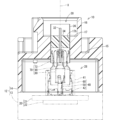
- FIG. 1 is a perspective view showing a device including a coaxial connector and a coaxial connector connection structure according to an embodiment.
- FIG. 2 is a cross-sectional view taken along line II-II of FIG.
- FIG. 3 is a perspective view showing a connection structure of a coaxial connector.
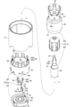
- FIG. 4 is an exploded perspective view showing the same connection structure.
- FIG. 5 is an enlarged cross-sectional view of FIG.
- FIG. 6 is a perspective view showing the tip of a coaxial connector.
- FIG. 7 is a cross-sectional view showing a connection structure of a coaxial connector that is connected at an angle.
- FIG. 8 is a partial cross-sectional view of FIG.
- FIG. 9 is a cross-sectional view of another portion of FIG.
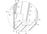
- FIG. 10 is a partial cross-sectional view showing an interference avoidance surface according to a modified example.
- the coaxial connector disclosed herein is as follows:
- a coaxial connector to be connected to a mating coaxial connector comprising an inner conductor and an outer conductor surrounding the outer periphery of the inner conductor, at least one of the inner conductor and the outer conductor having a tubular portion to which a mating terminal of the mating coaxial connector is connected, the tubular portion is connected to the mating terminal with the mating terminal disposed on the inner or outer periphery of the tubular portion, and a portion of the tip periphery of the tubular portion facing the mating terminal has an interference avoidance surface that is inclined away from the mating terminal as it approaches the tip of the tubular portion.
- the interference avoidance surface may extend in a ring shape along the periphery of the tip of the tubular portion.
- the coaxial connector is unlikely to interfere with the mating coaxial connector no matter in which direction it is tilted relative to the central axis of the mating coaxial connector.
- the interference avoidance surface may guide the elastic piece of the mating terminal at the tip edge of the tubular portion.
- the elastic piece is guided by the interference avoidance surface and can move smoothly to the inner or outer circumference of the cylindrical portion.
- the interference avoidance surface may be formed on one of the inner and outer circumferential sides of the tubular portion, and the surface on the other of the inner and outer circumferential sides of the tubular portion may be formed in a shape in which a portion of the same diameter is continuous along the central axis of the tubular portion.
- the end of the tube can be chamfered to easily form an interference-avoiding surface.
- the interference avoidance surface may be formed on one of the inner and outer circumferential sides of the cylindrical portion, and the other of the inner and outer circumferential sides of the cylindrical portion may be formed in a shape that is inclined in the same direction as the inclination of the interference avoidance surface.
- the end of the tube can be bent to easily form an interference avoidance surface.
- a slit may be formed on the peripheral edge of the tip of the cylindrical portion to separate the interference avoidance surface.
- the width of the slit may be smaller than the width of the elastic piece of the mating terminal.
- the inner peripheral portion of the tip periphery of the inner conductor tube will be more likely to interfere with the mating terminal. If an inner interference avoidance surface is formed on the inner peripheral portion of the tip periphery of the inner conductor tube as an interference avoidance surface, the inner peripheral portion of the tip periphery of the inner conductor tube will be less likely to interfere with the mating terminal even if the inner conductor is significantly tilted relative to the mating terminal.
- a coaxial connector according to any one of (1) to (8), wherein the outer conductor includes an outer conductor tube portion as the tube portion, the outer conductor tube portion is inserted into the mating terminal, and an outer interference avoidance surface is formed on the outer peripheral portion of the tip periphery of the outer conductor tube portion as the interference avoidance surface.
- connection structure of the coaxial connector disclosed herein is as follows:
- a coaxial connector connection structure comprising a coaxial connector according to any one of (1) to (9) and the mating coaxial connector, the mating coaxial connector having a mating inner conductor and a mating outer conductor surrounding the outer periphery of the mating inner conductor, the mating inner conductor having an inner elastic piece that elastically contacts the inner conductor, and the mating outer conductor having an outer elastic piece that elastically contacts the outer conductor.
- the mating inner conductor has an inner elastic piece that elastically contacts the inner conductor
- the mating outer conductor has an outer elastic piece that elastically contacts the outer conductor, so that by elastically deforming the inner elastic piece and the outer elastic piece, the coaxial connector can be connected to the mating coaxial connector even if the coaxial connector is tilted relative to the mating coaxial connector.
- the interference avoidance surface makes it difficult for the coaxial connector to interfere with the mating coaxial connector.
- the mating coaxial connector may have a mating dielectric located between the base end of the mating inner conductor and the base end of the mating outer conductor, and the mating dielectric may have an annular recess facing the coaxial connector.
- Fig. 1 is a perspective view showing a device 10 including a coaxial connector 70 and a coaxial connector connection structure 28.
- Fig. 2 is a cross-sectional view taken along line II-II in Fig. 1.
- the device 10 is, for example, a camera device.
- the camera device is, for example, a device mounted on a vehicle.
- the device 10 does not have to be a camera device.
- the device 10 comprises a case 12, an electrical component 20, and a coaxial connector for external connection 30.
- the electrical component 20 is housed inside the case 12.
- the coaxial connector for external connection 30 is a connector for connecting the electrical component 20 to an external electrical component.
- the coaxial connector for external connection 30 is a connector to which a cable connected to an external electrical component is connected.
- the case 12 comprises a first case 13 and a second case 14.
- the first case 13 and the second case 14 are formed, for example, from resin.
- the first case 13 and the second case 14 are combined to form the rectangular box-shaped case 12 that houses the electrical components 20. If the device 10 is a camera device, it is assumed that the first case 13 has a lens or window for capturing images, and the second case 14 has a coaxial connector 30 for external connection.
- a retaining tube portion 16 protrudes from the bottom 15 of the case 12.
- the retaining tube portion 16 is cylindrical and protrudes outward from the center of the bottom 15.
- the inner opening of the retaining tube portion 16 opens into the second case 14, and the outer opening of the retaining tube portion 16 opens to the outside of the second case 14.
- a retaining partition portion 17 is formed in the middle of the retaining tube portion 16 in the direction along the central axis X.
- the retaining partition portion 17 is formed in the middle of the retaining tube portion 16 in the direction along the central axis X, near the inner opening.
- the retaining partition portion 17 separates the space of the retaining tube portion 16 on the inner opening side from the space of the outer opening side.
- a retaining hole 17h is formed in the retaining partition portion 17, and the external connection coaxial connector 30 is inserted and held in the retaining hole 17h.
- the coaxial connector 30 for external connection comprises an inner conductor 32 for external connection, a dielectric 34 for external connection, and an outer conductor 36 for external connection.
- the external connection inner conductor 32 is formed in a long, thin rod shape and is made of a conductive material such as metal.
- the external connection inner conductor 32 is an example of a pin-shaped opposing inner conductor that is inserted and connected to the inner conductor 80 described below.
- the external connection dielectric 34 is formed of an insulator such as resin, and surrounds the external connection inner conductor 32.
- the external connection outer conductor 36 is formed of a conductive material such as metal.
- the external connection outer conductor 36 is formed in a cylindrical shape that surrounds the external connection dielectric 34.
- the external connection outer conductor 36 is an example of an opposing outer conductor to which the outer conductor 90 is connected.
- the electrical component 20 is, for example, a mounting board on which electronic components are mounted.
- the electrical component 20 is assumed to be a circuit board 21 and an image sensor 22 mounted on the circuit board 21.
- the image sensor 22 faces an image capturing lens or window in the first case 13, and captures the outside scenery by rotating the lens or window.
- the side of the first case 13 to which the image sensor 22 faces may be referred to as the front side, and the opposite side, the second case 14 side, may be referred to as the rear side.
- a coaxial connector connection structure 28 is incorporated into the device 10.
- the coaxial connector connection structure 28 is a connection structure between the board coaxial connector 40 and the coaxial connector 70.
- the coaxial connector for the board 40 is provided on the surface of the circuit board 21 opposite the imaging element 22.
- the coaxial connector for the board 40 is fixed to the circuit board 21.
- the coaxial connector for the board 40 is an example of a mating coaxial connector that is connected to the coaxial connector 70.
- the coaxial connector 40 for circuit boards comprises a mating inner conductor 50 and a mating outer conductor 60 that surrounds the outer periphery of the mating inner conductor 50.
- the coaxial connector 40 for circuit boards may further comprise a mating dielectric 42 located between the mating inner conductor 50 and the mating outer conductor 60.
- the mating dielectric 42 surrounds the mating inner conductor 50.
- the mating dielectric 42 is made of an insulator.
- the mating outer conductor 60 surrounds the mating dielectric 42.
- the base end of the mating inner conductor 50 and the base end of the mating outer conductor 60 are fixed to the circuit board 21 by soldering or the like.
- the mating inner conductor 50 and the mating outer conductor 60 are electrically connected to the circuit of the circuit board 21 and are fixed in a state protruding from the circuit board 21.
- the board coaxial connector 40 protrudes from the circuit board 21 toward the external connection coaxial connector 30.
- a coaxial connector 70 is connected to the coaxial connector for board 40.
- the coaxial connector 70 includes an inner conductor 80, an outer conductor 90 surrounding the outer periphery of the inner conductor 80, and a dielectric 72 located between the inner conductor 80 and the outer conductor 90.
- the dielectric 72 surrounds the periphery of the inner conductor 80.
- the dielectric 72 is composed of an insulator.
- the outer conductor 90 surrounds the periphery of the dielectric 72.
- the coaxial connector 70 is connected to the coaxial connector for board 40 with the mating inner conductor 50 inserted and connected to the inner conductor 80 and the outer conductor 90 inserted and connected to the mating outer conductor 60.
- the coaxial connector 70 further protrudes from the coaxial connector for board 40 toward the coaxial connector for external connection 30.
- the coaxial connector 70 relays and connects the coaxial connector for board 40 and the coaxial connector for external connection 30.
- the coaxial connector 70 is connected to the coaxial connector for board 40 and the coaxial connector for external connection 30 in a manner that allows it to change its position.
- the coaxial connector 70 may be understood as a relay coaxial connector.
- the coaxial connector 30 for external connection is provided on the second case 14 side, i.e., the rear side of the case 12. Inside the case 12, a coaxial connector 70 is connected to the coaxial connector 30 for external connection.
- an external cable is connected to the coaxial connector 30 for external connection, an external electrical component to which the cable is connected is electrically connected to the electrical component 20 inside the case 12.
- the circuit board 21 is supported at a fixed position within the case 12.
- the position of the board coaxial connector 40 relative to the external connection coaxial connector 30 is set to a fixed position.
- the position of the board coaxial connector 40 relative to the external connection coaxial connector 30 may deviate from the designed position.
- the insertion amount of the coaxial connector 70 into the coaxial connector for board 40 can be adjusted within a range in which the mating inner conductor 50 and the inner conductor 80 can maintain electrical contact, and the mating outer conductor 60 and the outer conductor 90 can maintain electrical contact.
- the coaxial connector 70 can be inserted and connected in a tilted state relative to the coaxial connector for board 40 and the coaxial connector for external connection 30.
- the distance change can be absorbed by adjusting the insertion amount of the coaxial connector 70 into the coaxial connector for board 40.
- the tilt of the coaxial connector 70 relative to the coaxial connector for board 40 and the coaxial connector for external connection 30 absorbs the positional shift.
- a part of the peripheral tip of the outer conductor 90 on the circuit board 21 side may approach the mating outer conductor 60 and interfere with the mating outer conductor 60.
- a part of the peripheral tip of the inner conductor 80 on the circuit board 21 side may approach the mating inner conductor 50 and interfere with the mating inner conductor 50.
- the inclination of the coaxial connector 70 relative to the coaxial connector 40 for the board is greatest when, within the tolerance range, the coaxial connector 70 is closest to the coaxial connector 40 for the board and the coaxial connector 30 for external connection is most displaced from the position coaxially facing the coaxial connector 40 for the board.
- the inclination of the coaxial connector 70 relative to the coaxial connector 40 for the board is at its greatest, there is a strong demand to avoid interference of the coaxial connector 70 with the coaxial connector 40 for the board.
- the inner conductor 80 and the outer conductor 90 are designed to ensure a reliable connection and to obtain the desired communication performance, taking into account the relative positional relationship of the coaxial connectors 40, 70, which may vary within the tolerance range. For this reason, it may be difficult to avoid the above-mentioned interference by shortening the protruding length of the tip periphery of the inner conductor 80 and the outer conductor 90.
- Fig. 3 is a perspective view showing the coaxial connector connection structure 28.
- Fig. 4 is an exploded perspective view showing the same connection structure.
- Fig. 5 is an enlarged cross-sectional view of Fig. 3.
- Fig. 6 is a perspective view showing the tip of the coaxial connector 70. In Fig. 6, the elastic pieces 56, 66 are partially shown.
- the coaxial connector for circuit board 40 includes the mating inner conductor 50 , the mating outer conductor 60 , and the mating dielectric 42 .
- the mating inner conductor 50 is an elongated conductive member.
- the mating inner conductor 50 is formed by pressing a metal plate.
- the first inner conductor may also be formed by cutting a metal material.
- the mating inner conductor 50 includes a mating inner conductor tube portion 52 and an inner elastic piece 56.
- the mating inner conductor tube portion 52 is formed in a tubular shape, more specifically, in a cylindrical shape.
- the base end of the mating inner conductor 50 is accommodated and held in the mating dielectric 42.
- the tip is the end to which the coaxial connector 70 is connected, and the base end is the end opposite the tip, in this case the end facing the circuit board 21.
- a positioning piece 53 is formed so as to protrude outward from a circumferential portion at the base end of the mating inner conductor tube portion 52.
- the positioning piece 53 is a plate-shaped portion that follows the central axis of the mating inner conductor tube portion 52, and in this embodiment is a rectangular plate-shaped portion.
- the positioning piece 53 is configured with two overlapping plate-shaped portions.
- the mating inner conductor tube portion 52 is formed by pressing the plate-shaped portions into a tube.
- a plate-shaped portion protrudes outward from each of two adjacent edges at the joint of the tube, and the positioning piece 53 is formed by the overlap of the two plate-shaped portions.
- a retaining projection 53p that hooks onto the bottom of the positioning groove 44 of the opposing dielectric 42 is formed on the protruding end 53e of the positioning piece 53.
- the retaining projection 53p is formed in a shape that hooks onto the bottom of the positioning groove 44 so that the opposing inner conductor tube portion 52 is less likely to slip out toward the tip side of the opposing dielectric 42.
- the retaining projection 53p is formed in a triangular plate shape.
- the edge of the retaining projection 53p on the tip side of the opposing inner conductor tube portion 52 is more inclined with respect to the central axis X than the edge of the retaining projection 53p on the base side of the opposing inner conductor tube portion 52.
- the positioning piece 53 and the retaining projection 53p may be omitted.
- the mating inner conductor tube portion 52 may be formed with a locking piece 52a that hooks onto the inner peripheral surface of the mating dielectric 42 when pressed into the mating dielectric 42.
- a protruding piece 52b that extends along the main surface of the circuit board 21 and is used for soldering may be provided at the base end of the mating inner conductor tube portion 52.
- An inner elastic piece 56 protrudes from the tip of the mating inner conductor tube portion 52.
- multiple (three in this example) inner elastic pieces 56 extend from the tip of the mating inner conductor tube portion 52 at intervals in the circumferential direction.
- the multiple inner elastic pieces 56 are positioned at equal intervals around the central axis X of the mating inner conductor tube portion 52.
- the inner elastic piece 56 includes an inclined portion 56a that inclines outward from the tip of the mating inner conductor tube portion 52, and a curved portion 56b that is connected to the tip of the inclined portion 56a and has an outwardly convex curved shape.
- the inclined portions 56a elastically deform inward, while the outward apex of the curved portions 56b is elastically pressed against the inner circumferential surface of the inner conductor 80.
- the inner elastic pieces 56 elastically contact the inner conductor 80, and the mating inner conductor 50 is kept electrically connected to the inner conductor 80.
- the number of elastic pieces may be two or four or more.
- the opposing dielectric 42 is formed into a disk shape from resin or the like.
- the maximum thickness dimension of the opposing dielectric 42 is smaller than the length dimension of the opposing inner conductor tube portion 52.
- the opposing dielectric 42 is, for example, a molded resin part.
- an insertion hole 43 is formed into which the base end of the opposing inner conductor 50, more specifically, the base end of the opposing inner conductor tube portion 52, is inserted.
- a positioning groove 44 is formed into which a positioning piece 53 is fitted. The positioning groove 44 is recessed from a portion of the circumference of the insertion hole 43 toward the outer periphery and is formed as a groove extending along the central axis X.
- the mating inner conductor tube portion 52 is inserted into the insertion hole 43, so that the mating inner conductor 50 is inserted and held in the mating dielectric 42.
- the mating inner conductor tube portion 52 is press-fitted and held in the insertion hole 43.
- the above press-fit structure makes it easier to hold the mating inner conductor firmly against the mating dielectric.
- the mating inner conductor 50 is a pressed metal plate product, a positioning piece 53 is fitted into the positioning groove 44 to increase the holding strength. The inner surface of the positioning groove 44 clamps the positioning piece 53, making it easier for the mating dielectric 42 to hold the mating inner conductor 50 firmly.
- the anti-slip projection 53p of the positioning piece 53 hooks into the bottom of the positioning groove 44, making it difficult for the mating inner conductor 50 to slip out of the mating dielectric 42, and the mating inner conductor 50 is held more firmly in place.
- a retaining annular protrusion 45 that protrudes annularly toward the tip of the mating inner conductor 50 is formed in the portion of the mating dielectric 42 that surrounds the insertion hole 43.
- the retaining annular protrusion 45 holds the mating inner conductor tube portion 52, so that the mating inner conductor 50 is held more firmly and the mating inner conductor 50 is less likely to tilt relative to the mating dielectric 42.
- the outer peripheral surface of the mating dielectric 42 is formed in a short cylindrical shape that can be inserted into the inner peripheral portion of the mating outer conductor 60.
- An outer peripheral portion of the mating dielectric 42 on the mating outer conductor 60 side is formed with an outer peripheral annular protrusion 46 that protrudes in an annular shape toward the tip side of the mating inner conductor 50.
- the outer peripheral surface of the mating dielectric 42 is formed wide in the direction of the central axis X by the outer peripheral annular protrusion 46. Therefore, the outer peripheral surface of the mating dielectric 42 can face the inner peripheral surface of the mating outer conductor 60 over a wide area.
- the portion of the mating dielectric 42 that faces the coaxial connector 70 has an annular recess 47 that is recessed between the retaining annular protrusion 45 on the inner circumference of the mating dielectric 42 and the outer peripheral annular protrusion 46 on the outer circumference.
- the mating outer conductor 60 is made of a conductive material such as metal, and surrounds the mating dielectric 42. Therefore, the mating dielectric 42 is a cylindrical member interposed between the mating inner conductor 50 and the mating outer conductor 60.
- the mating outer conductor 60 is formed, for example, by pressing a metal plate.
- the mating outer conductor 60 includes a mating outer conductor tube portion 62 and an outer elastic piece 66 that protrudes from the tip of the mating outer conductor tube portion 62.
- the opposing outer conductor tube portion 62 is formed in a tubular shape, more specifically, a cylindrical shape, inside which the opposing dielectric 42 can be placed.
- the opposing dielectric 42 is housed and held in the base end portion of the opposing outer conductor tube portion 62.
- the opposing outer conductor tube portion 62 may be formed with a locking piece 62a that hooks onto the outer peripheral surface of the opposing dielectric 42 when the opposing dielectric 42 is pressed in.
- An outer elastic piece 66 protrudes from the tip of the mating outer conductor tube portion 62.
- multiple (eight in this embodiment) outer elastic pieces 66 extend from the tip of the mating outer conductor tube portion 62 at intervals in the circumferential direction.
- the multiple outer elastic pieces 66 are positioned at equal intervals around the central axis X of the mating outer conductor tube portion 62.
- the outer elastic piece 66 includes an inclined portion 66a that slopes inward from the tip of the mating outer conductor tube portion 62, and a curved portion 66b that is connected to the tip of the inclined portion 66a and has an inwardly convex curved shape.
- the inclined portions 66a elastically deform outward, while the inward apex of the curved portions 66b is elastically pressed against the outer peripheral surface of the outer conductor 90.
- the outer elastic pieces 66 elastically contact the outer conductor 90, and the mating outer conductor 60 is kept electrically connected to the outer conductor 90.
- the number of elastic pieces may be seven or less, or nine or more.
- the length dimension of the mating outer conductor tube portion 62 is greater than the thickness dimension of the mating dielectric 42. In this embodiment, the length dimension of the mating outer conductor tube portion 62 is greater than the length dimension of the mating inner conductor 50.
- the base end of the outer elastic piece 66 is located farther away from the mating dielectric 42 than the base end of the inner elastic piece 56. Furthermore, the tip of the outer elastic piece 66 is located farther away from the mating dielectric 42 than the tip of the inner elastic piece 56.
- the curved portions 56b, 66b can contact the inner conductor 80 or the outer conductor 90 at the same position in the central axis X.
- the coaxial connector 40 for the board may be surrounded by a cylindrical connector holder 41.
- the connector holder 41 is a member formed of resin or the like, and serves to surround the coaxial connector 40 for the board from all sides and prevent it from coming into contact with other members.
- the coaxial connector 70 comprises the inner conductor 80 , the outer conductor 90 , and the dielectric 72 .
- the inner conductor 80 is an elongated conductive member.
- the inner conductor 80 is formed by pressing a metal plate. More specifically, the inner conductor 80 includes an inner conductor tube portion 82 and an inner conductor extension tube portion 86.
- the inner conductor tube portion 82 is formed in a tubular shape, more specifically, in a cylindrical shape.
- the open end of the inner conductor tube portion 82 faces the side of the coaxial connector for board 40.
- the inner conductor tube portion 82 is the portion that is connected to the mating inner conductor 50.
- the inner conductor tube portion 82 is a long, thin tube extending along the central axis X.
- the inner diameter of the inner conductor tube portion 82 is smaller than the outer diameter of an imaginary circle connecting the tops of the multiple inner elastic pieces 56.
- the multiple inner elastic pieces 56 can elastically contact the inner peripheral surface of the inner conductor tube portion 82 while elastically deforming inward.
- the inner conductor tube portion 82 is longer than the inner elastic piece 56.
- the apex of the curved portion 56b of the inner elastic piece 56 can contact any position on the inner surface of the inner conductor tube portion 82, thereby connecting the mating inner conductor 50 and the inner conductor 80. This makes it possible to accommodate misalignment between the mating inner conductor 50 and the inner conductor 80 in the direction of the central axis X.
- the inner conductor extension tube portion 86 is located on the opposite side of the inner conductor tube portion 82 from the coaxial connector for circuit board 40. In this embodiment, the inner conductor extension tube portion 86 is thinner than the inner conductor tube portion 82.
- the inner conductor extension tube portion 86 is connected to the inner conductor tube portion 82 via a tapered portion 81.
- the tapered portion 81 is a tapered portion that gradually becomes thinner from the inner conductor tube portion 82 toward the inner conductor extension tube portion 86.
- the inner conductor extension tube portion may be connected to the inner conductor tube portion via a step portion.
- the inner conductor extension tube portion 86 may have an elastic piece 87 that protrudes toward the tip side.
- the elastic piece 87 is configured to be elastically deformable in the inward and outward directions.
- the inner conductor for external connection 32 is inserted between the two elastic pieces 87 from the tip side of the two elastic pieces 87.
- the inner conductor for external connection 32 is sandwiched between the two elastic pieces 87, and the inner conductor 80 is connected to the inner conductor for external connection 32.
- the inner conductor extension tube portion 86 may be formed with a partial locking piece 86a that can be locked to the dielectric 72.
- the dielectric 72 is made of resin or the like.
- the dielectric 72 is, for example, a molded resin part.
- the dielectric 72 is formed in a tubular shape capable of accommodating at least a portion of the inner conductor 80.
- the dielectric 72 is formed in a cylindrical shape.
- the inner conductor extension tubular portion 86 is accommodated within the dielectric 72.
- the internal space of the inner conductor extension tubular portion 86 is large enough to hold the base end of the inner conductor extension tubular portion 86 in a pressed-in state and to allow elastic deformation of the elastic piece 87 in the inward and outward directions.
- the dielectric 72 can be positioned relative to the inner conductor 80 by contacting one end of the dielectric 72 with the tapered portion 81.
- the inner conductor tube portion 82 extends further toward the coaxial connector for circuit board 40 than the dielectric 72.
- the outer conductor 90 is disposed on the outer periphery of the dielectric 72.
- the outer conductor 90 is formed from a conductive material such as metal, and surrounds the dielectric 72.
- the outer conductor 90 is formed, for example, by pressing a metal plate.
- the outer conductor 90 comprises an outer conductor tube portion 92 and an outer conductor extension tube portion 96.
- the outer conductor tube portion 92 is formed in a tubular shape, more specifically, in a cylindrical shape.
- the open end of the outer conductor tube portion 92 faces the coaxial connector for board 40 side.
- the outer conductor tube portion 92 is the portion that is connected to the mating outer conductor 60.
- the outer conductor tube portion 92 is positioned on the outer periphery of the inner conductor tube portion 82 with a gap therebetween.
- the outer diameter of the outer conductor tube portion 92 is larger than the outer diameter of an imaginary circle connecting the tops of the multiple outer elastic pieces 66.
- the multiple outer elastic pieces 66 can elastically contact the outer periphery of the outer conductor tube portion 92 while elastically deforming outward.
- the outer conductor tube portion 92 is longer than the outer elastic piece 66.
- the top of the curved portion 66b of the outer elastic piece 66 can come into contact with any position on the outer peripheral surface of the outer conductor tube portion 92, thereby connecting the mating outer conductor 60 and the outer conductor 90. This makes it possible to accommodate misalignment between the mating outer conductor 60 and the outer conductor 90 in the direction of the central axis X.
- the outer conductor extension tube portion 96 is located on the opposite side of the outer conductor tube portion 92 from the coaxial connector for board 40. In this embodiment, the outer conductor extension tube portion 96 is thinner than the outer conductor tube portion 92.
- the outer conductor extension tube portion 96 is connected to the outer conductor tube portion 92 via a tapered portion 91.
- the tapered portion 91 is a tapered portion that gradually becomes thinner from the outer conductor tube portion 92 toward the outer conductor extension tube portion 96.
- the outer conductor extension tube portion may be connected to the outer conductor tube portion via a step portion.
- the outer conductor extension tube portion 96 may have an elastic piece 97 that protrudes toward the tip side.
- the elastic piece 97 is configured to be elastically deformable in the inward and outward directions.
- the external connection outer conductor 36 is fitted onto the outer periphery of the multiple elastic pieces 97 from the tip side of the multiple elastic pieces 97.
- the multiple elastic pieces 97 are elastically pressed against the inner peripheral surface of the external connection outer conductor 36, thereby connecting the outer conductor 90 to the external connection outer conductor 36.
- the outer conductor extension tube portion 96 may be formed with a partial locking piece 96a that can be locked to the dielectric 72.
- At least one of the inner conductor 80 and the outer conductor 90 has a cylindrical portion 82, 92 to which a mating terminal of the coaxial connector for board 40 is connected.
- the mating inner conductor 50 of the coaxial connector for board 40 is an example of a mating terminal
- the mating outer conductor 60 is also an example of a mating terminal.
- the inner conductor 80 has an inner conductor tube portion 82 as a tube portion.
- the inner conductor tube portion 82 is connected to the mating inner conductor 50 as a mating terminal, with the mating inner conductor 50 being disposed on the inner circumference side of the inner conductor tube portion 82.
- the outer conductor 90 has an outer conductor tube portion 92 as a tube portion.
- the outer conductor tube portion 92 is connected to the mating outer conductor 60 as a mating terminal, with the mating outer conductor 60 being disposed on the outer periphery of the outer conductor tube portion 92.
- the portion of the tip periphery of the tubular portion 82, 92 that faces the mating terminal, the mating inner conductor 50 or the mating outer conductor 60, has an interference avoidance surface 83, 93.
- the interference avoidance surface 83, 93 is formed as a surface that slopes away from the mating terminal, the mating inner conductor 50 or the mating outer conductor 60, as it approaches the tip side of the tubular portion 82, 92.
- the following description focuses on the interference avoidance surface 83 of the inner conductor tube portion 82.
- the inner conductor tube portion 82 is located closer to the mating inner conductor 50 than to the mating outer conductor 60. Therefore, when the coaxial connector 70 is tilted relative to the coaxial connector for circuit board 40, the tip edge of the inner conductor tube portion 82 is more likely to come into contact with the mating inner conductor 50 than with the mating outer conductor 60.
- the interference avoidance surface 83 is therefore formed on the inner peripheral portion of the tip periphery of the inner conductor tube portion 82 that faces the inner elastic piece 56. Furthermore, the interference avoidance surface 83 is formed on a surface that slopes away from the inner elastic piece 56 as it approaches the tip side of the inner conductor tube portion 82. In other words, the interference avoidance surface 83 is formed so as to slope outward as it approaches the tip side of the inner conductor tube portion 82.
- the interference avoidance surface 83 may also be referred to as an inner interference avoidance surface 83.
- the interference avoidance surface 83 preferably extends in an annular shape along the periphery of the tip of the inner conductor tube portion 82. In this case, interference between the inner conductor tube portion 82 and the mating inner conductor 50 can be easily avoided even if the inner conductor tube portion 82 is tilted in any direction relative to the mating inner conductor 50.
- the interference avoidance surface 83 may have a recess 83a formed therein that does not reach the base end of the interference avoidance surface 83.
- the recess 83a that does not reach the base end of the interference avoidance surface 83 does not negate the continuity of the interference avoidance surface 83 that extends in an annular shape along the tip periphery of the inner conductor tube portion 82.
- the interference avoidance surface 83 may be formed with a slit 83b to facilitate processing.
- the slit 83b (see FIG. 6) has a width S1 that is smaller than the width W1 of the inner elastic piece 56, and does not negate the continuity of the interference avoidance surface 83 that extends in a ring shape along the tip periphery of the inner conductor tube portion 82.
- the interference avoidance surface 83 extend in a ring shape along the tip periphery of the inner conductor tube portion 82.
- the interference avoidance surface may be formed at a partial location on the tip periphery of the inner conductor tube portion 82 that may interfere with the mating inner conductor due to the inclination.
- the interference avoidance surface 83 is preferably formed at a position that guides the inner elastic piece 56 on the peripheral tip edge of the inner conductor tube portion 82.
- the interference avoidance surface 83 is formed at the same position as the inner elastic piece around the central axis X.
- the interference avoidance surface 83 extends in an overall ring shape along the periphery of the tip of the inner conductor tube portion 82, the interference avoidance surface 83 can guide the inner elastic piece 56 regardless of the connection position of the coaxial connector 70 and the coaxial connector for circuit board 40 around the central axis X.
- the interference avoidance surface 83 may be a surface formed on the inner circumference of the tip periphery of the inner conductor tube portion 82, and the method of formation is not important.
- the interference avoidance surface 83 may be formed by cutting the inner circumference of the tip periphery of the inner conductor tube portion 82, rolling the tip periphery of the inner conductor tube portion 82 so that it becomes thinner toward the tip, pressing and bending the tip periphery of the inner conductor tube portion 82, or a combination of these processes.
- the interference avoidance surface 83 is formed by pressing and bending the peripheral tip edge of the inner conductor tube portion 82. In this case, both the inner and outer peripheral surfaces of the peripheral tip edge of the inner conductor tube portion 82 are bent in the same direction. As a result, the outer peripheral surface portion of the inner conductor tube portion 82 opposite the interference avoidance surface 83 is formed into a shape that is inclined along the outer peripheral side of the interference avoidance surface 83.
- the interference avoidance surface 83 is formed by pressing and bending the peripheral edge of the tip of the inner conductor tube portion 82, the interference avoidance surface 83 can be easily bent significantly.
- the outer conductor tube portion 92 is located between the mating inner conductor 50 and the mating outer conductor 60, closer to the mating outer conductor 60 than to the mating inner conductor 50. Therefore, when the coaxial connector 70 is tilted relative to the coaxial connector for circuit board 40, the tip edge of the outer conductor tube portion 92 is more likely to come into contact with the mating outer conductor 60 than with the mating inner conductor 50.
- the interference avoidance surface 93 is therefore formed on the outer peripheral portion of the tip periphery of the outer conductor tube portion 92 that faces the outer elastic piece 66. Furthermore, the interference avoidance surface 93 is formed on a surface that slopes away from the outer elastic piece 66 as it approaches the tip side of the outer conductor tube portion 92. In other words, the interference avoidance surface 93 is formed so as to slope inward as it approaches the tip side of the outer conductor tube portion 92.
- the interference avoidance surface 93 may also be referred to as an outer interference avoidance surface 93.
- the interference avoidance surface 93 preferably extends in a ring shape along the periphery of the tip of the outer conductor tube portion 92. In this case, interference between the outer conductor tube portion 92 and the mating outer conductor 60 can be easily avoided even if the outer conductor tube portion 92 is tilted in any direction relative to the mating outer conductor 60.
- the interference avoidance surface 93 may have recesses 93a, 93b formed thereon that do not reach the base end of the interference avoidance surface 93.
- the recesses 93a, 93b that do not reach the base end of the interference avoidance surface 93 do not negate the continuity of the interference avoidance surface 93 that extends in an annular shape along the tip periphery of the outer conductor tube portion 92.
- the interference avoidance surface 93 extend in a ring shape along the tip periphery of the outer conductor tube portion 92.
- the interference avoidance surface may be formed at a partial location on the tip periphery of the outer conductor tube portion 92 that may interfere with the mating outer conductor due to the inclination.
- the interference avoidance surface 93 is preferably formed at a position that guides the outer elastic piece 66 on the tip periphery of the outer conductor tube portion 92.
- the interference avoidance surface 93 is formed at the same position as the outer elastic piece around the central axis X.
- the interference avoidance surface 93 extends in a ring shape along the periphery of the tip of the outer conductor tube portion 92, the interference avoidance surface 93 can guide the outer elastic piece 66 regardless of the connection position of the coaxial connector 70 and the coaxial connector for circuit board 40 around the central axis X.
- the interference avoidance surface 93 may be a surface formed on the outer periphery of the tip periphery of the outer conductor tube portion 92, and the method of formation is not limited.
- the interference avoidance surface 93 may be formed by cutting the outer periphery of the tip periphery of the outer conductor tube portion 92, rolling the tip periphery of the outer conductor tube portion 92 so that it becomes thinner toward the tip, or bending the tip periphery of the outer conductor tube portion 92 by pressing (e.g., drawing).
- the interference avoidance surface 83 is formed by cutting the outer periphery of the tip periphery of the outer conductor tube portion 92.
- the process of cutting the outer periphery of the tip periphery of the outer conductor tube portion 92 to form the interference avoidance surface 93 may be a process called chamfering.
- the inner peripheral portion of the outer conductor tube portion 92 on the side opposite to the interference avoidance surface 93 is formed into a shape in which a portion of the same diameter is continuous along the central axis X of the outer conductor tube portion 92.
- the inner peripheral surface of the outer conductor tube portion 92 retains the initial shape that was obtained when the outer conductor tube portion 92 was processed into a circular shape.
- the inner periphery of the outer conductor tube portion 92 on the side opposite the interference avoidance surface 93 is formed in a shape in which the same diameter portion is continuous along the central axis X, the distance between the outer conductor tube portion 92 and the central axis X is easily maintained constant. This makes it possible to reduce the change in distance between the inner and outer conductors, making it easier to maintain good communication performance in the coaxial connector connection structure 28.
- the inclination of the interference avoidance surface 83 relative to the central axis X is greater than the inclination of the interference avoidance surface 93 relative to the central axis X.
- the length of the interference avoidance surface 83 in the direction along the central axis X is shorter than the length of the interference avoidance surface 93 in the direction along the central axis X.
- the tip edges of the tube sections 82 and 92 are each formed with an appropriate interference-avoiding shape.
- the inclination of the interference avoidance surfaces 83, 93 relative to the central axis X and the length in the direction along the central axis X should be set to a value that can avoid interference between the two coaxial connectors 40, 70, taking into account the maximum inclination angle of the coaxial connector 70 relative to the coaxial connector for circuit board 40 that can occur within the tolerance range.
- the multiple inner elastic pieces 56 come into contact with the interference avoidance surface 83 of the inner conductor tube portion 82, and as a result, the multiple inner elastic pieces 56 are displaced inward and smoothly guided to the inner peripheral surface at the rear of the inner conductor tube portion 82 (see arrow P1 in FIG. 5).
- the multiple outer elastic pieces 66 come into contact with the interference avoidance surface 93 of the outer conductor tube portion 92, and as a result, the multiple outer elastic pieces 66 are displaced outward and smoothly guided to the outer peripheral surface at the rear of the outer conductor tube portion 92 (see arrow P2 in FIG. 5).
- the central axis X of the coaxial connector 40 for the board coincides with the central axis X of the coaxial connector 70, and the distance between the coaxial connector 40 for the board and the coaxial connector 70 is kept at a specified design distance (see Figure 5).
- Figure 7 is a cross-sectional view of the connection structure 28 when the coaxial connector 70 is closest to the coaxial connector 40 for the board, and the coaxial connector 30 for external connection is most displaced from the position coaxially facing the coaxial connector 40 for the board, within the tolerance range.
- Figures 8 and 9 are partial cross-sectional views of Figure 7.
- the distance L2 of the coaxial connector 70 relative to the coaxial connector 40 for the board is smaller than the initial design distance L1 by a distance L3. Also, the central axis Xa of the coaxial connector 70 is spaced a distance L4 from the central axis X of the coaxial connector 40 for the board.
- part of the peripheral tip of the inner conductor 80 on the circuit board 21 side approaches the mating inner conductor 50. Also, part of the peripheral tip of the outer conductor 90 on the circuit board 21 side approaches the mating outer conductor 60. For this reason, if the peripheral tips of the inner conductor tube portion 82 and the outer conductor tube portion 92 remain in their initial shapes without interference avoidance surfaces, they may come into contact with the outer conductor 90 or the inner conductor 80, respectively (see parts B1 and B2 indicated by two-dot chain lines in Figures 8 and 9).
- interference avoidance surfaces 83, 93 are formed on the inner conductor tube portion 82 and the outer conductor tube portion 92, respectively, so that the tip edges of the inner conductor tube portion 82 and the outer conductor tube portion 92 are effectively prevented from coming into contact with the outer conductor 90 or the inner conductor 80.
- the inner conductor tube portion 82 may approach the mating dielectric 42.
- the tip edge of the inner conductor tube portion 82 may enter the annular recess 47 of the mating dielectric 42. This also avoids interference between the inner conductor tube portion 82 and the mating dielectric 42.
- the inner conductor tube portion 182 and the outer conductor tube portion 192 may be formed as in the modified example shown in FIG. 10. That is, the inner conductor tube portion 182 and the outer conductor tube portion 192 each have a slit 183a, 193a formed along the central axis X. At least one slit 183a, 193a may be provided for each of the inner conductor tube portion 182 and the outer conductor tube portion 192.
- a plurality of slits 183a, 193a may be provided for each of the inner conductor tube portion 182 and the outer conductor tube portion 192, and in this case, a plurality of slits may be provided at equal intervals in the circumferential direction.
- the number, width, and length of the slits 183a, 193a may be set to a degree that does not cause deformation of the inner conductor tube portion 182 and the outer conductor tube portion 192 when connected.
- the tip edge of the inner conductor tube portion 182 is widened toward the outer periphery by widening the slit 183a.
- the inner periphery of the portion widened toward the outer periphery serves as the interference avoidance surface 183, which corresponds to the interference avoidance surface 83.
- the outer conductor tube portion 192 has its tip edge narrowed toward the inner circumference by narrowing the slit 193a.
- the outer circumference of the portion narrowed toward the inner circumference serves as the interference avoidance surface 193, which corresponds to the interference avoidance surface 93.
- the slits 183a, 193a can be used to widen the tip periphery of the inner conductor tube portion 182 and the outer conductor tube portion 192 toward the outer circumference or narrow it toward the inner circumference, making it easier to incline the interference avoidance surfaces 183, 193 at a large angle and over a wide range, and as a result, it is easier to set a large amount of avoidance for interference avoidance.
- the widths S1, S2 of the slits 183a, 193a are smaller than the width W1 of the inner elastic piece 56 and the width W3 of the outer elastic piece 66. This allows the inner elastic piece 56 and the outer elastic piece 66 to move smoothly over the inner surface of the inner conductor tube portion 182 or the outer surface of the outer conductor tube portion 192 without entering the slits 183a, 193a.
- the portion of the tip periphery of the tubular portions 82, 92 that faces the mating terminal, the mating inner conductor 50 or the mating outer conductor 60, is inclined away from the mating inner conductor 50 or the mating outer conductor 60 toward the tip side of the tubular portions 82, 92. Therefore, even if the tip periphery of the tubular portions 82, 92 approaches the mating inner conductor 50 or the mating outer conductor 60, contact with the mating inner conductor 50 or the mating outer conductor 60 is suppressed. As a result, even if the coaxial connector 70 is inclined with respect to the central axis X of the coaxial connector for board 40, the coaxial connector 70 is unlikely to interfere with the coaxial connector for board 40.
- the interference avoidance surfaces 83, 93 extend in an annular shape along the tip periphery of the tubular portions 82, 92, the coaxial connector 70 is unlikely to interfere with the coaxial connector for circuit board 40, regardless of the direction in which the coaxial connector 70 is tilted relative to the central axis X of the coaxial connector for circuit board 40.
- the interference avoidance surfaces 83, 93 are formed at a position on the tip periphery of the tubular portions 82, 92 that guides the inner elastic piece 56 or the outer elastic piece 66, the inner elastic piece 56 or the outer elastic piece 66 can be guided by the interference avoidance surfaces 83, 93 and move smoothly to the inner or outer periphery of the tubular portions 82, 92.
- the interference avoidance surface 93 can be easily formed by chamfering the end of the outer conductor tube portion 92, etc.
- the interference avoidance surface 83 can be easily formed, for example, by bending the end of the inner conductor tube portion 82.
- slits 83b, 183a, 193a are formed on the tip periphery of the inner conductor tube portion 82, 182 or the outer conductor tube portion 192, dividing the interference avoidance surface 83, 183, 193, it is easy to form the divided interference avoidance surface 83, 183, 193 over the entire tip periphery of the inner conductor tube portion 82, 182 or the outer conductor tube portion 192.
- the widths S1 and S of the slits 83b, 183a and 193a are smaller than the width W1 of the inner elastic piece 56 or the width W2 of the outer elastic piece 66, the inner elastic piece 56 or the outer elastic piece 66 will not fit into the slits 83b, 183a and 193a, but will be smoothly guided to the inner circumference of the inner conductor tube portion 82 and 182 or the outer circumference of the outer conductor tube portion 192.
- an inner interference avoidance surface 83 is formed on the inner peripheral portion of the tip periphery of the inner conductor tube portion 82, so even if the inner conductor 80 is significantly tilted relative to the mating inner conductor 50, the inner peripheral portion of the tip periphery of the inner conductor tube portion 82 is unlikely to interfere with the mating inner conductor 50.
- an external interference avoidance surface 93 is formed on the outer peripheral portion of the tip periphery of the outer conductor tube portion 92, so even if the outer conductor 90 is significantly tilted relative to the mating outer conductor 60, the outer peripheral portion of the tip periphery of the outer conductor tube portion 92 is unlikely to interfere with the mating outer conductor 60.
- the mating inner conductor 50 has an inner elastic piece 56
- the mating outer conductor 60 has an outer elastic piece 66. Therefore, by elastically deforming the inner elastic piece 56 and the outer elastic piece 66, the coaxial connector 70 can be connected to the coaxial connector 40 for the board, even if the coaxial connector 70 is tilted relative to the coaxial connector 40 for the board. In this case, even if the coaxial connector 70 is tilted relative to the coaxial connector 40 for the board, the interference avoidance surfaces 83, 93 make it difficult for the coaxial connector 70 to interfere with the coaxial connector 40 for the board.
- the mating dielectric 42 has an annular recess 47, even if the coaxial connector 70 is connected to the coaxial connector for circuit board 40 in an inclined state, the outer conductor tube portion 92 is unlikely to interfere with the mating dielectric 42.
- the thickness of the inner and outer periphery of the mating dielectric 42 is ensured, so that the mating outer conductor 60 and the mating inner conductor 50 are firmly held against the mating dielectric 42.
Landscapes
- Coupling Device And Connection With Printed Circuit (AREA)
Abstract
同軸コネクタが相手側同軸コネクタの中心軸に対して傾いても、同軸コネクタが相手側同軸コネクタに干渉し難くすることを目的とする。同軸コネクタは、相手側同軸コネクタに接続される同軸コネクタであって、内導体と、内導体の外周側を囲む外導体とを備える。内導体および外導体の少なくとも一方は、相手側同軸コネクタの相手側端子が接続される筒部を有し、筒部は、相手側端子が筒部の内周側または外周側に配置された状態で、相手側端子に接続され、筒部の先端周縁のうち相手側端子と対向する部分は、筒部の先端側に向かうに連れて相手側端子から遠ざかる側に傾斜する干渉回避面を有する。
Description
本開示は、同軸コネクタおよび同軸コネクタの接続構造に関する。
特許文献1は、第一同軸コネクタと、第二同軸コネクタと、第三同軸コネクタとを有する同軸コネクタ組立体を開示している。特許文献1は、第一同軸コネクタと第二同軸コネクタとの間と、第二同軸コネクタと第三同軸コネクタとの間とがいずれも、軸線方向と半径方向とで相対移動可能なフローティング構造を形成していることを開示している。
一対の同軸コネクタ同士で、半径方向のずれが大きくなると、一方の同軸コネクタに対する他方の同軸コネクタの傾きが大きくなる。この場合、両同軸コネクタ同士が干渉する可能性がある。
そこで、本開示は、同軸コネクタが相手側同軸コネクタの中心軸に対して傾いても、同軸コネクタが相手側同軸コネクタに干渉し難くすることを目的とする。
本開示の同軸コネクタは、相手側同軸コネクタに接続される同軸コネクタであって、内導体と、前記内導体の外周側を囲む外導体と、を備え、前記内導体および前記外導体の少なくとも一方は、前記相手側同軸コネクタの相手側端子が接続される筒部を有し、前記筒部は、前記相手側端子が前記筒部の内周側または外周側に配置された状態で、前記相手側端子に接続され、前記筒部の先端周縁のうち前記相手側端子と対向する部分は、前記筒部の先端側に向かうに連れて前記相手側端子から遠ざかる側に傾斜する干渉回避面を有する、同軸コネクタである。
本開示によれば、同軸コネクタが相手側同軸コネクタの中心軸に対して傾いても、同軸コネクタが相手側同軸コネクタに干渉し難くできる。
[本開示の実施形態の説明]
最初に本開示の実施態様を列記して説明する。
最初に本開示の実施態様を列記して説明する。
本開示の同軸コネクタは、次の通りである。
(1)相手側同軸コネクタに接続される同軸コネクタであって、内導体と、前記内導体の外周側を囲む外導体と、を備え、前記内導体および前記外導体の少なくとも一方は、前記相手側同軸コネクタの相手側端子が接続される筒部を有し、前記筒部は、前記相手側端子が前記筒部の内周側または外周側に配置された状態で、前記相手側端子に接続され、前記筒部の先端周縁のうち前記相手側端子と対向する部分は、前記筒部の先端側に向かうに連れて前記相手側端子から遠ざかる側に傾斜する干渉回避面を有する、同軸コネクタである。
同軸コネクタを相手側同軸コネクタに接続する際に、同軸コネクタが相手側同軸コネクタの中心軸に対して傾くと、筒部の先端周縁が相手側端子に近づく可能性がある。本同軸コネクタによると、筒部の先端周縁のうち相手側端子と対向する部分は、筒部の先端側に向かうに連れて相手側端子から遠ざかる側に傾斜している。このため、筒部の先端周縁が相手側端子に近づいても、当該相手側端子との接触が抑制される。これにより、同軸コネクタが相手側同軸コネクタの中心軸に対して傾いても、同軸コネクタが相手側同軸コネクタに干渉し難い。
(2)(1)の同軸コネクタであって、前記干渉回避面は、前記筒部の先端周縁に沿って環状に延在してもよい。
この場合、同軸コネクタが相手側同軸コネクタの中心軸に対してどの方向に傾いても、同軸コネクタが相手側同軸コネクタに干渉し難い。
(3)(1)または(2)の同軸コネクタであって、前記干渉回避面は、前記筒部の先端周縁において前記相手側端子の弾性片をガイドしてもよい。
この場合、弾性片が干渉回避面によってガイドされて筒部の内周側または外周側に円滑に移動できる。
(4)(1)から(3)のいずれか1つの同軸コネクタであって、前記筒部の内周側および外周側のうちの一方に前記干渉回避面が形成され、前記筒部の内周側および外周側のうちの他方側の面は、前記筒部の中心軸に沿って同径部分が連続する形状に形成されていてもよい。
この場合、例えば、筒部の端部を面取り加工することによって、干渉回避面を容易に形成できる。
(5)(1)から(4)のいずれか1つの同軸コネクタであって、前記筒部の内周側および外周側のうちの一方に前記干渉回避面が形成され、前記筒部の内周側および外周側のうちの他方側の面は、前記干渉回避面の傾斜と同じ側に傾斜する形状に形成されていてもよい。
この場合、例えば、筒部の端部を曲げ加工することによって、干渉回避面を容易に形成できる。
(6)(5)の同軸コネクタであって、前記筒部の先端周縁に、前記干渉回避面を分断するスリットが形成されていてもよい。
これにより、筒部の先端周縁の全体に、スリットで分割された干渉回避面を容易に形成できる。
(7)(6)の同軸コネクタであって、前記スリットの幅は、前記相手側端子の弾性片の幅よりも小さくてもよい。
これにより、弾性片が、スリットに嵌らないで筒部の内周側または外周側に円滑にガイドされる。
(8)(1)から(7)のいずれか1つの同軸コネクタであって、前記内導体は、前記筒部としての内導体筒部を含み、前記内導体筒部には、前記相手側端子が挿入され、前記内導体筒部の先端周縁のうちの内周部分には、前記干渉回避面としての内干渉回避面が形成されていてもよい。
内導体筒部に、相手側端子が挿入される場合、相手側端子に対して内導体が大きく傾くと、内導体筒部の先端周縁のうちの内周部分が相手側端子に干渉し易くなることが考えられる。内導体筒部の先端周縁のうちの内周部分に、干渉回避面としての内干渉回避面が形成されていると、相手側端子に対して内導体が大きく傾いても、内導体筒部の先端周縁のうちの内周部分が相手側端子に干渉し難い。
(9)(1)から(8)のいずれか1つの同軸コネクタであって、前記外導体は、前記筒部としての外導体筒部を含み、前記外導体筒部は、前記相手側端子に挿入され、前記外導体筒部の先端周縁のうちの外周部分には、前記干渉回避面としての外干渉回避面が形成されていてもよい。
外導体筒部に、相手側端子が挿入される場合、相手側端子に対して外導体が大きく傾くと、外導体筒部の先端周縁のうちの外周部分が相手側端子に干渉し易くなることが考えられる。外導体筒部の先端周縁のうちの外周部分に、干渉回避面としての外干渉回避面が形成されていると、相手側端子に対して外導体が大きく傾いても、筒部の先端周縁のうちの外周部分が相手側端子に干渉し難い。
また、本開示の同軸コネクタの接続構造は次の通りである。
(10)(1)から(9)のいずれか1つの同軸コネクタと、前記相手側同軸コネクタと、を備え、前記相手側同軸コネクタは、相手側内導体と、前記相手側内導体の外周側を囲む相手側外導体と、を有し、前記相手側内導体は、前記内導体に弾性的に接触する内側弾性片を有し、前記相手側外導体は、前記外導体に弾性的に接触する外側弾性片を有する、同軸コネクタの接続構造である。
この場合、相手側内導体が内導体に弾性的に接触する内側弾性片を有し、相手側外導体が外導体に弾性的に接触する外側弾性片を有するため、内側弾性片と外側弾性片とを弾性変形させることで、相手側同軸コネクタに対して同軸コネクタが傾いていても、相手側同軸コネクタに対して同軸コネクタを接続できる。この場合に、干渉回避面によって、同軸コネクタが相手側同軸コネクタに干渉し難くできる。
(11)(10)の同軸コネクタの接続構造であって、前記相手側同軸コネクタは、前記相手側内導体の基端部と前記相手側外導体の基端部との間に位置する相手側誘電体を有し、前記相手側誘電体は、前記同軸コネクタと対向する環状凹部を有してもよい。
この場合、相手側誘電体に環状凹部が形成されているので、相手側同軸コネクタに対して同軸コネクタが傾いた状態で接続されても、外導体筒部が相手側誘電体に干渉し難い。
[本開示の実施形態の詳細]
本開示の同軸コネクタおよび同軸コネクタの接続構造の具体例を、以下に図面を参照しつつ説明する。なお、本開示はこれらの例示に限定されるものではなく、請求の範囲によって示され、請求の範囲と均等の意味および範囲内でのすべての変更が含まれることが意図される。
本開示の同軸コネクタおよび同軸コネクタの接続構造の具体例を、以下に図面を参照しつつ説明する。なお、本開示はこれらの例示に限定されるものではなく、請求の範囲によって示され、請求の範囲と均等の意味および範囲内でのすべての変更が含まれることが意図される。
[実施形態]
以下、実施形態に係る同軸コネクタの接続構造について説明する。図1は同軸コネクタ70および同軸コネクタの接続構造28を備える機器10を示す斜視図である。図2は図1のII-II線断面図である。
以下、実施形態に係る同軸コネクタの接続構造について説明する。図1は同軸コネクタ70および同軸コネクタの接続構造28を備える機器10を示す斜視図である。図2は図1のII-II線断面図である。
<機器の全体構成について>
機器10は、例えば、カメラ機器である。カメラ機器は、例えば、車載用の機器である。機器10は、カメラ機器でなくてもよい。
機器10は、例えば、カメラ機器である。カメラ機器は、例えば、車載用の機器である。機器10は、カメラ機器でなくてもよい。
機器10は、ケース12と、電気部品20と、外部接続用同軸コネクタ30とを備える。ケース12内に電気部品20が収容されている。外部接続用同軸コネクタ30は、電気部品20と、外部の電気部品とを接続するためのコネクタである。例えば、外部接続用同軸コネクタ30は、外部の電気部品に接続されたケーブルが接続されるコネクタである。
ケース12は、第1ケース13と、第2ケース14とを備えている。第1ケース13および第2ケース14は、例えば、樹脂によって形成される。第1ケース13と第2ケース14とが合体することで、電気部品20を収容する直方体箱状のケース12が構成される。機器10がカメラ機器である場合、第1ケース13は撮像用のレンズまたは窓を有しており、第2ケース14が外部接続用同軸コネクタ30を有していることが想定される。
より具体的には、ケース12の底部15に保持筒部16が突設されている。保持筒部16は、円筒であり、底部15の中央部から外側に突出している。保持筒部16の内側開口は第2ケース14内に開口し、保持筒部16の外側開口は第2ケース14外に開口している。保持筒部16の中心軸Xに沿った方向の中間部に保持仕切部17が形成されている。本実施形態では、保持筒部16の中心軸Xに沿った方向の中間であって内側開口寄りの位置に保持仕切部17が形成されている。保持仕切部17は、保持筒部16のうち内側開口側の空間と、外側開口側の空間とを仕切っている。保持仕切部17に保持孔17hが形成されており、当該保持孔17hに外部接続用同軸コネクタ30が挿入されて保持される。
外部接続用同軸コネクタ30は、外部接続用内導体32と、外部接続用誘電体34と、外部接続用外導体36とを備える。
外部接続用内導体32は、細長い棒状に形成されており、金属等の導電材料によって形成されている。外部接続用内導体32は、後述する内導体80に挿入接続されるピン状の反対相手側内導体の一例である。外部接続用誘電体34は、樹脂等の絶縁体によって形成されており、外部接続用内導体32の周りを囲んでいる。外部接続用外導体36は、金属等の導電材料によって形成されている。外部接続用外導体36は、外部接続用誘電体34の周りを囲む筒状に形成されている。外部接続用外導体36は、外導体90が接続される反対相手側外導体の一例である。
電気部品20は、例えば、基板に電子部品が実装された実装基板である。機器10がカメラ機器である場合、電気部品20は、回路基板21と、当該回路基板21に実装された撮像素子22であることが想定される。撮像素子22は、第1ケース13の撮像用のレンズまたは窓に対向し、当該レンズまたは窓を回して外側景色を撮像する。以下、撮像素子22が向く第1ケース13側を前側、それとは反対側の第2ケース14側を後側という場合がある。
機器10に同軸コネクタの接続構造28が組込まれる。同軸コネクタの接続構造28は、基板用同軸コネクタ40と同軸コネクタ70との接続構造である。
本実施形態では、回路基板21のうち撮像素子22とは反対側の面に基板用同軸コネクタ40が設けられる。基板用同軸コネクタ40は、回路基板21に固定される。基板用同軸コネクタ40は、同軸コネクタ70に接続される相手側同軸コネクタの一例である。
基板用同軸コネクタ40は、相手側内導体50と、相手側内導体50の外周側を囲む相手側外導体60とを備える。基板用同軸コネクタ40は、相手側内導体50と相手側外導体60との間に位置する相手側誘電体42をさらに備えてもよい。
相手側誘電体42は、相手側内導体50の周囲を囲んでいる。相手側誘電体42は、絶縁体によって形成されている。相手側誘電体42の周囲を相手側外導体60が囲んでいる。相手側内導体50の基端部と相手側外導体60の基端部とが回路基板21にはんだ付け等によって固定される。これより、相手側内導体50と相手側外導体60とが回路基板21の回路に電気的に接続されると共に、回路基板21から突出した状態で固定される。基板用同軸コネクタ40は、回路基板21から外部接続用同軸コネクタ30に向けて突出している。
基板用同軸コネクタ40に同軸コネクタ70が接続される。同軸コネクタ70は、内導体80と、内導体80の外周側を囲む外導体90と、内導体80と外導体90との間に位置する誘電体72とを含む。誘電体72は、内導体80の周囲を囲んでいる。誘電体72は、絶縁体によって構成されている。誘電体72の周囲を外導体90が囲んでいる。相手側内導体50が内導体80に挿入接続されると共に、外導体90が相手側外導体60に挿入接続された状態で、同軸コネクタ70が基板用同軸コネクタ40に接続されている。同軸コネクタ70は、基板用同軸コネクタ40からさらに外部接続用同軸コネクタ30に向けて突出している。同軸コネクタ70が、基板用同軸コネクタ40と外部接続用同軸コネクタ30とを中継接続する。同軸コネクタ70は、基板用同軸コネクタ40および外部接続用同軸コネクタ30に対して姿勢変更可能に接続される。同軸コネクタ70は、中継用同軸コネクタと把握されてもよい。
外部接続用同軸コネクタ30は、第2ケース14側、即ち、ケース12の後側に設けられる。ケース12内で、同軸コネクタ70が外部接続用同軸コネクタ30に接続されている。外部からのケーブルが、当該外部接続用同軸コネクタ30に接続されることで、当該ケーブルの接続先である外部の電気部品と、ケース12内の電気部品20とが電気的に接続される。
ケース12内において回路基板21は一定位置に支持される。設計上は、外部接続用同軸コネクタ30に対する基板用同軸コネクタ40の位置は一定位置に設定される。しかしながら、公差範囲内で、外部接続用同軸コネクタ30に対する基板用同軸コネクタ40の位置が設計上の位置からずれる可能性がある。
本実施形態では、基板用同軸コネクタ40に対する同軸コネクタ70の挿入量は、相手側内導体50と内導体80とが電気的接触を維持でき、かつ、相手側外導体60と外導体90とが電気的接触を維持できる範囲で、調整可能である。また、同軸コネクタ70は、基板用同軸コネクタ40および外部接続用同軸コネクタ30に対して傾いた状態で挿入接続可能である。これにより、本機器10の組付作業時または完成状態において、基板用同軸コネクタ40に対する外部接続用同軸コネクタ30の距離が変動したとしても、基板用同軸コネクタ40に対する同軸コネクタ70の挿入量を調整することで、当該距離変動を吸収できる。また、外部接続用同軸コネクタ30が、基板用同軸コネクタ40に対して同軸上で対向する位置からずれていたとしても、基板用同軸コネクタ40および外部接続用同軸コネクタ30に対して同軸コネクタ70が傾くことで、当該位置ずれが吸収される。
基板用同軸コネクタ40に対する同軸コネクタ70の傾きが大きくなると、外導体90のうち回路基板21側の先端周縁の1部が相手側外導体60に接近し、当該相手側外導体60に干渉する可能性がある。また、内導体80のうち回路基板21側の先端周縁の1部が相手側内導体50に接近し、当該相手側内導体50に干渉する可能性がある。
例えば、公差範囲内で、同軸コネクタ70が基板用同軸コネクタ40に対して最も接近し、かつ、外部接続用同軸コネクタ30が、基板用同軸コネクタ40に対して同軸上で対向する位置から最もずれた場合に、基板用同軸コネクタ40に対する同軸コネクタ70の傾きが最も大きくなると考えられる。基板用同軸コネクタ40に対する同軸コネクタ70の傾きが最も大きくなった状態で、基板用同軸コネクタ40に対する同軸コネクタ70の干渉を回避する要請が大きい。
なお、公差範囲内で変動し得る同軸コネクタ40、70の相対位置関係を想定して、接続が確実になされ、かつ、所望の通信性能が得られるように、内導体80および外導体90の設計がなされる。このため、内導体80および外導体90の先端周縁の突出長を短くすることでは、上記干渉を回避することは困難な場合が想定され得る。
基板用同軸コネクタ40と同軸コネクタ70との接続構造を前提として、上記干渉を回避するための構成について説明する。
<同軸コネクタの接続構造について>
同軸コネクタの接続構造28についてより具体的に説明する。図3は同軸コネクタの接続構造28を示す斜視図である。図4は同接続構造を示す分解斜視図である。図5は図3の拡大断面図である。図6は同軸コネクタ70の先端を示す斜視図である。図6において弾性片56、66が部分的に示されている。
同軸コネクタの接続構造28についてより具体的に説明する。図3は同軸コネクタの接続構造28を示す斜視図である。図4は同接続構造を示す分解斜視図である。図5は図3の拡大断面図である。図6は同軸コネクタ70の先端を示す斜視図である。図6において弾性片56、66が部分的に示されている。
基板用同軸コネクタ40および同軸コネクタ70のそれぞれについてより具体的に説明してから、干渉を回避するための構造についてより具体的に説明する。
<基板用同軸コネクタについて>
上記したように基板用同軸コネクタ40は、相手側内導体50と、相手側外導体60と、相手側誘電体42とを含む。
上記したように基板用同軸コネクタ40は、相手側内導体50と、相手側外導体60と、相手側誘電体42とを含む。
相手側内導体50は、細長い導電性部材である。本実施形態では、相手側内導体50は、金属板をプレス加工することによって形成されている。なお、第1内導体は、金属材を切削加工することによって形成されてもよい。
より具体的には、相手側内導体50は、相手側内導体筒部52と、内側弾性片56とを含む。
相手側内導体筒部52は、筒状、より具体的には、円筒状に形成されている。相手側内導体50の基端部は、相手側誘電体42に収容保持される。なお、基板用同軸コネクタ40において、先端とは同軸コネクタ70が接続される側の端であり、基端とは当該先端の反対側の端、ここでは、回路基板21を向く側の端である。
相手側内導体筒部52の基端部における周方向の1部から外周側に突出するように位置決め片53が形成されている。位置決め片53は、相手側内導体筒部52の中心軸に沿う板状部分であり、本実施形態では、方形板状部分である。位置決め片53は、2枚の板状部分が重なった構成とされている。本実施形態では、板状部分が筒をなすようにプレス加工されることで相手側内導体筒部52が形成される。当該筒の継目で隣接する2つの縁部のそれぞれから板状部分が外周側に突出しており、当該2つの板状部分が重なることで位置決め片53が形成されている。
位置決め片53の突出端部53eに、相手側誘電体42の位置決め溝44の底に引っ掛る抜止め突起53pが形成されている。抜止め突起53pは、相手側内導体筒部52が相手側誘電体42に対して先端側に抜け難くなるように位置決め溝44の底に引っ掛る形状に形成されている。ここでは、抜止め突起53pは、三角板状に形成されている。抜止め突起53pのうち相手側内導体筒部52の先端側の縁は、抜止め突起53pのうち相手側内導体筒部52の基端側の縁よりも、中心軸Xに対して大きく傾いている。このため、抜止め突起53pを位置決め溝44に対して相手側内導体筒部52の基端側に圧入し易く、かつ、相手側内導体筒部52の先端側に抜け難くできる。上記位置決め片53および抜止め突起53pは、省略されてもよい。
上記相手側内導体筒部52に、相手側誘電体42への圧入時に当該相手側誘電体42の内周面に引っ掛る係止片52aが形成されてもよい。上記相手側内導体筒部52の基端に回路基板21の主面に沿って延びて、はんだ付のために利用される突出片52bが設けられてもよい。
相手側内導体筒部52の先端から内側弾性片56が突出している。本実施形態では、複数(ここでは3つ)の内側弾性片56が、相手側内導体筒部52の先端から周方向において間隔をあけて延出している。好ましくは、複数の内側弾性片56は、相手側内導体筒部52の中心軸X周りに等間隔で位置する。
内側弾性片56は、相手側内導体筒部52の先端から外向き傾斜する傾斜部56aと、当該傾斜部56aの先端部に連なり外向きに凸をなす湾曲形状をなす湾曲部56bとを含む。
複数の内側弾性片56が内導体80に挿入されると、傾斜部56aが内側に弾性変形しつつ、湾曲部56bの外向きの頂部が、内導体80の内周面に弾性的に押付けられる。これにより、内側弾性片56が内導体80に弾性的に接触して、相手側内導体50が内導体80に電気的に接続された状態に保たれる。
なお、弾性片は2つであってもよいし、4つ以上であってもよい。
相手側誘電体42は、樹脂等によって円板状に形成されている。相手側誘電体42の最大厚み寸法は、相手側内導体筒部52の長さ寸法よりも小さい。相手側誘電体42は、例えば、金型成形樹脂部品である。
相手側誘電体42の中央に、相手側内導体50の基端部、より具体的には、相手側内導体筒部52の基端部が挿入される挿入孔43が形成されている。また、位置決め片53が嵌め込まれる位置決め溝44が形成されている。位置決め溝44は、挿入孔43の周方向の1部から外周側に向かって凹み、かつ、中心軸Xに沿って延びる溝に形成されている。
そして、挿入孔43に相手側内導体筒部52が挿入されることで、相手側内導体50が相手側誘電体42に対して挿入保持される。好ましくは、相手側内導体筒部52が挿入孔43に圧入保持される。
相手側内導体が切削加工品であれば、上記圧入構造によって相手側誘電体に対して相手側内導体をしっかり保持し易い。相手側内導体50が金属板のプレス加工品である場合、保持強度を高めるため、位置決め片53が位置決め溝44に嵌め込まれる。位置決め溝44の内周面が位置決め片53を挟持することによって、相手側誘電体42が相手側内導体50をしっかり保持し易くなる。
また、位置決め片53の上記抜止め突起53pが位置決め溝44の底に食込むように引っ掛ることで、相手側内導体50が相手側誘電体42から抜出難くなり、相手側内導体50がよりしっかりと保持される。
また、相手側誘電体42のうち挿入孔43を囲む部分に、相手側内導体50の先端側に向かって環状に突出する保持環状凸部45が形成されている。保持環状凸部45が相手側内導体筒部52を保持することで、相手側内導体50がよりしっかりと保持され、また、相手側内導体50が相手側誘電体42に対して傾き難い。
相手側誘電体42の外周面は、相手側外導体60の内周部に挿入可能な短円柱周面形状に形成されている。相手側誘電体42のうち相手側外導体60側の外周部分に、相手側内導体50の先端側に向かって環状に突出する外周環状凸部46が形成されている。相手側誘電体42の外周面は、外周環状凸部46の分、中心軸X方向において広く形成されている。このため、相手側誘電体42の外周面は、広い面積で、相手側外導体60の内周面に対向することができる。これにより、相手側外導体60に対して相手側誘電体42がしっかりと保持され易く、かつ、相手側誘電体42に対して相手側外導体60が傾き難い。これにより、相手側内導体50と相手側外導体60とが同軸上の位置関係に保たれ易い。
相手側誘電体42のうち同軸コネクタ70と対向する部分に、相手側誘電体42の内周部の保持環状凸部45と外周部の外周環状凸部46との間で凹む環状凹部47が形成されている。
基板用同軸コネクタ40に対して同軸コネクタ70が大きく傾いた状態で、外導体90の先端周縁が相手側誘電体42に接近し過ぎると、当該先端周縁が環状凹部47内に入り込むことができる。
相手側外導体60は、金属等の導電材料によって形成されており、相手側誘電体42の周りを囲んでいる。よって、相手側誘電体42は、相手側内導体50と相手側外導体60との間に介在する筒状の部材である。相手側外導体60は、例えば、金属板をプレス加工等することによって形成される。
本実施形態では、相手側外導体60は、相手側外導体筒部62と、相手側外導体筒部62の先端から突出する外側弾性片66とを含む。
相手側外導体筒部62は、内側に相手側誘電体42を配置可能な筒状、より具体的には、円筒状に形成されている。相手側誘電体42が、相手側外導体筒部62の基端部分に収容保持される。
相手側外導体筒部62に、相手側誘電体42の圧入時に当該相手側誘電体42の外周面に引っ掛る係止片62aが形成されてもよい。
相手側外導体筒部62の先端から外側弾性片66が突出している。本実施形態では、複数(ここでは8つ)の外側弾性片66が、相手側外導体筒部62の先端から周方向において間隔をあけて延出している。好ましくは、複数の外側弾性片66は、相手側外導体筒部62の中心軸X周りに等間隔で位置する。
外側弾性片66は、相手側外導体筒部62の先端から内向き傾斜する傾斜部66aと、当該傾斜部66aの先端部に連なり内向きに凸をなす湾曲形状をなす湾曲部66bとを含む。
複数の外側弾性片66が外導体90に外嵌めされると、傾斜部66aが外側に弾性変形しつつ、湾曲部66bの内向きの頂部が、外導体90の外周面に弾性的に押付けられる。これにより、外側弾性片66が外導体90に弾性的に接触し、相手側外導体60が外導体90に電気的に接続された状態に保たれる。
なお、弾性片は7つ以下であってもよいし、9つ以上であってもよい。
中心軸X方向において、相手側外導体筒部62の長さ寸法は、相手側誘電体42の厚み寸法よりも大きい。また、本実施形態では、相手側外導体筒部62の長さ寸法は、相手側内導体50の長さ寸法よりも大きい。また、相手側誘電体42に対して、外側弾性片66の基端は、内側弾性片56の基端よりも離れて位置する。さらに、相手側誘電体42に対して、外側弾性片66の先端は、内側弾性片56の先端よりも離れて位置する。但し、湾曲部56b、66bは、中心軸Xにおいて同じ位置で内導体80または外導体90に接触できる。
基板用同軸コネクタ40は、筒状のコネクタホルダ41によって囲まれていてもよい。コネクタホルダ41は、樹脂等によって形成された部材であり、当該基板用同軸コネクタ40を周りから囲って、他の部材への接触を抑制する役割を果す。
<同軸コネクタについて>
上記したように、同軸コネクタ70は、内導体80と、外導体90と、誘電体72とを備える。
上記したように、同軸コネクタ70は、内導体80と、外導体90と、誘電体72とを備える。
内導体80は、細長い導電性部材である。本実施形態では、内導体80は、金属板をプレス加工することによって形成されている。より具体的には、内導体80は、内導体筒部82と、内導体延長筒部86とを含む。
内導体筒部82は、筒状、より具体的には、円筒状に形成されている。内導体筒部82の開口端は、基板用同軸コネクタ40側を向いている。内導体筒部82は、相手側内導体50に接続される部分である。
より具体的には、内導体筒部82は、中心軸Xに沿って細長い筒である。内導体筒部82の内径は、複数の内側弾性片56の頂部を結ぶ仮想円の外径よりも小さい。複数の内側弾性片56が、内側に弾性変形しつつ、内導体筒部82の内周面に弾性的に接触できる。
中心軸X方向において、内導体筒部82は、内側弾性片56よりも長い。中心軸X方向において、内導体筒部82の内周面の任意の位置に、内側弾性片56の湾曲部56bの頂部が接触することで、相手側内導体50と内導体80とが接続され得る。これにより、中心軸X方向における、相手側内導体50と内導体80との位置ずれに対応できる。
内導体延長筒部86は、上記内導体筒部82に対して基板用同軸コネクタ40とは反対側に位置している。本実施形態では、内導体延長筒部86は、内導体筒部82よりも細い。内導体延長筒部86は、内導体筒部82に対してテーパ部81を介して連なっている。テーパ部81は、内導体筒部82から内導体延長筒部86に向けて徐々に細くなるテーパ形状部分である。内導体延長筒部は、内導体筒部に対して段部を介して連なっていてもよい。
内導体延長筒部86は、先端側に向けて突出する弾性片87を有していてもよい。弾性片87は、内外方向に弾性変形可能に構成されている。外部接続用内導体32が、2つの弾性片87の先端側から当該2つの弾性片87間に向けて挿入される。外部接続用内導体32が、当該2つの弾性片87によって挟込まれた状態となることで、内導体80が外部接続用内導体32に接続される。
内導体延長筒部86に、誘電体72に係止可能な部分的な係止片86aが形成されてもよい。
誘電体72は、樹脂等によって形成されている。誘電体72は、例えば、金型成形樹脂部品である。
誘電体72は、内導体80の少なくとも一部を収容可能な筒状に形成されている。本実施形態では、誘電体72は、円筒状に形成されている。誘電体72内に、内導体延長筒部86が収容される。内導体延長筒部86の内部空間は、内導体延長筒部86の基端部を圧入状態で保持でき、かつ、弾性片87の内外方向への弾性変形を許容できる程度の大きさに形成されている。
誘電体72の一端が、テーパ部81に接することで、内導体80に対する誘電体72の位置決めがなされ得る。内導体筒部82は、誘電体72よりも基板用同軸コネクタ40側に延出している。
誘電体72の外周側に外導体90が配置される。外導体90は、金属等の導電材料によって形成されており、誘電体72の周りを囲んでいる。外導体90は、例えば、金属板をプレス加工等することによって形成される。
外導体90は、外導体筒部92と、外導体延長筒部96とを備える。
外導体筒部92は、筒状、より具体的には、円筒状に形成されている。外導体筒部92の開口端は、基板用同軸コネクタ40側を向いている。外導体筒部92は、相手側外導体60に接続される部分である。
外導体筒部92は、内導体筒部82の外周側に間隔をあけて位置する。外導体筒部92の外径は、複数の外側弾性片66の頂部を結ぶ仮想円の外径よりも大きい。複数の外側弾性片66が、外側に弾性変形しつつ、外導体筒部92の外周面に弾性的に接触できる。
中心軸X方向において、外導体筒部92は、外側弾性片66よりも長い。中心軸X方向において、外導体筒部92の外周面の任意の位置に、外側弾性片66の湾曲部66bの頂部が接触することで、相手側外導体60と外導体90とが接続され得る。これにより、中心軸X方向における、相手側外導体60と外導体90との位置ずれに対応できる。
外導体延長筒部96は、上記外導体筒部92に対して基板用同軸コネクタ40とは反対側に位置している。本実施形態では、外導体延長筒部96は、外導体筒部92よりも細い。外導体延長筒部96は、外導体筒部92に対してテーパ部91を介して連なっている。テーパ部91は、外導体筒部92から外導体延長筒部96に向けて徐々に細くなるテーパ形状部分である。外導体延長筒部は、外導体筒部に対して段部を介して連なっていてもよい。
外導体延長筒部96は、先端側に向けて突出する弾性片97を有していてもよい。弾性片97は、内外方向に弾性変形可能に構成されている。外部接続用外導体36が、複数の弾性片97の先端側から当該複数の弾性片97の外周に外嵌めされる。複数の弾性片97が外部接続用外導体36の内周面に弾性的に押付けられることで、外導体90が外部接続用外導体36に接続される。
外導体延長筒部96に、誘電体72に係止可能な部分的な係止片96aが形成されてもよい。
<干渉回避のための構成について>
内導体80と外導体90との少なくとも一方は、基板用同軸コネクタ40の相手側端子が接続される筒部82、92を有する。本実施形態では、基板用同軸コネクタ40の相手側内導体50が相手側端子の一例であり、相手側外導体60も相手側端子の一例である。
内導体80と外導体90との少なくとも一方は、基板用同軸コネクタ40の相手側端子が接続される筒部82、92を有する。本実施形態では、基板用同軸コネクタ40の相手側内導体50が相手側端子の一例であり、相手側外導体60も相手側端子の一例である。
内導体80が筒部として内導体筒部82を有する。当該内導体筒部82は、相手側端子としての相手側内導体50が内導体筒部82の内周側に配置された状態で、当該相手側内導体50に接続される。
外導体90が筒部として外導体筒部92を有する。当該外導体筒部92は、相手側端子としての相手側外導体60が外導体筒部92の外周側に配置された状態で、当該相手側外導体60に接続される。
筒部82、92の先端周縁のうち相手側端子としての相手側内導体50または相手側外導体60に対向する部分は、干渉回避面83、93を有する。干渉回避面83、93は、筒部82、92の先端側に向かうに連れて相手側端子としての相手側内導体50、相手側外導体60から遠ざかる側に傾斜する面に形成されている。
内導体筒部82の干渉回避面83に着目して説明する。内導体筒部82は、相手側内導体50と相手側外導体60との間において、相手側外導体60よりも相手側内導体50の近くに位置する。このため、基板用同軸コネクタ40に対して同軸コネクタ70が傾いた場合、内導体筒部82の先端周縁は、相手側外導体60よりも相手側内導体50に接触し易い。
そこで、干渉回避面83は、内導体筒部82の先端周縁のうち内側弾性片56側を向く内周部分に形成されている。また、干渉回避面83は、内導体筒部82の先端側に向かうにつれて内側弾性片56から遠ざかる側に傾斜する面に形成されている。換言すれば、干渉回避面83は、内導体筒部82の先端側に向うにつれて外向き傾斜するように形成されている。干渉回避面83は、内干渉回避面83と称されてもよい。
干渉回避面83は、内導体筒部82の先端周縁に沿って環状に延在することが好ましい。この場合、相手側内導体50に対して内導体筒部82があらゆる方向に傾いても、内導体筒部82と相手側内導体50との干渉を回避しやすい。
干渉回避面83には、干渉回避面83の基端に達し無い程度の凹み83aが形成されていてもよい。干渉回避面83の基端に達し無い程度の凹み83aは、内導体筒部82の先端周縁に沿って環状に延在する干渉回避面83の連続性を否定しない。
干渉回避面83には、加工を容易にするためのスリット83bが形成されていてもよい。内側弾性片56の幅W1よりも小さい程度の幅S1のスリット83bは(図6参照)、内導体筒部82の先端周縁に沿って環状に延在する干渉回避面83の連続性を否定しない。
干渉回避面83が内導体筒部82の先端周縁に沿って環状に延在することは必須ではない。例えば、基板用同軸コネクタ40に対する同軸コネクタ70の傾き方向が決っている場合、干渉回避面は、内導体筒部82の先端周縁のうち当該傾きによって相手側内導体に干渉し得る部分的な箇所に形成されていてもよい。
干渉回避面83は、内導体筒部82の先端周縁において内側弾性片56をガイドする位置に形成されていることが好ましい。例えば、中心軸X周りにおいて、同軸コネクタ70と基板用同軸コネクタ40との接続姿勢が一定である場合、中心軸X周りにおいて、内側弾性片と同じ位置に干渉回避面83が形成されるとよい。
干渉回避面83が内導体筒部82の先端周縁に沿って全体的に環状に延在すれば、中心軸X周りにおける、同軸コネクタ70と基板用同軸コネクタ40との接続姿勢を問わず、干渉回避面83は、内側弾性片56をガイドできる。
干渉回避面83は、内導体筒部82の先端周縁の内周部に形成された面であればよく、その形成方法は問わない。例えば、干渉回避面83は、内導体筒部82の先端周縁の内周部を削ったり、内導体筒部82の先端周縁を先端に向うほど薄くなるように圧延したり、内導体筒部82の先端周縁をプレス加工して曲げたりしたり、これらの加工を組合わせたりすることによって形成されてもよい。
本実施形態では、内導体筒部82の先端周縁をプレス加工して曲げることによって干渉回避面83が形成されている。この場合、内導体筒部82の先端周縁の内周面も外周面も同じ方向に曲げられる。このため、内導体筒部82のうち干渉回避面83とは反対側の外周面部分は、干渉回避面83の外周側で当該干渉回避面83に沿って傾斜する形状に形成される。
内導体筒部82の先端周縁をプレス加工して曲げることによって干渉回避面83を形成すれば、当該干渉回避面83を大きく曲げ易い。
外導体筒部92の干渉回避面93に着目して説明する。
外導体筒部92は、相手側内導体50と相手側外導体60との間において、相手側内導体50よりも相手側外導体60の近くに位置する。このため、基板用同軸コネクタ40に対して同軸コネクタ70が傾いた場合、外導体筒部92の先端周縁は、相手側内導体50よりも相手側外導体60に接触し易い。
そこで、干渉回避面93は、外導体筒部92の先端周縁のうち外側弾性片66側を向く外周部分に形成されている。また、干渉回避面93は、外導体筒部92の先端側に向かうにつれて外側弾性片66から遠ざかる側に傾斜する面に形成されている。換言すれば、干渉回避面93は、外導体筒部92の先端側に向うにつれて内向き傾斜するように形成されている。干渉回避面93は、外干渉回避面93と称されてもよい。
干渉回避面93は、外導体筒部92の先端周縁に沿って環状に延在することが好ましい。この場合、相手側外導体60に対して外導体筒部92があらゆる方向に傾いても、外導体筒部92と相手側外導体60との干渉を回避しやすい。
干渉回避面93には、干渉回避面93の基端に達し無い程度の凹み93a、93bが形成されていてもよい。干渉回避面93の基端に達し無い程度の凹み93a、93bは、外導体筒部92の先端周縁に沿って環状に延在する干渉回避面93の連続性を否定しない。
干渉回避面93が外導体筒部92の先端周縁に沿って環状に延在することは必須ではない。例えば、基板用同軸コネクタ40に対する同軸コネクタ70の傾き方向が決っている場合、干渉回避面は、外導体筒部92の先端周縁のうち当該傾きによって相手側外導体に干渉し得る部分的な箇所に形成されていてもよい。
干渉回避面93は、外導体筒部92の先端周縁において外側弾性片66をガイドする位置に形成されていることが好ましい。例えば、中心軸X周りにおいて、同軸コネクタ70と基板用同軸コネクタ40との接続姿勢が一定である場合、中心軸X周りにおいて、外側弾性片と同じ位置に干渉回避面93が形成されるとよい。
干渉回避面93が外導体筒部92の先端周縁に沿って環状に延在すれば、中心軸X周りにおける、同軸コネクタ70と基板用同軸コネクタ40との接続姿勢を問わず、干渉回避面93は、外側弾性片66をガイドできる。
干渉回避面93は、外導体筒部92の先端周縁の外周部に形成された面であればよく、その形成方法は問わない。例えば、干渉回避面93は、外導体筒部92の先端周縁の外周部を削ったり、外導体筒部92の先端周縁を先端に向うほど薄くなるように圧延したり、外導体筒部92の先端周縁をプレス加工(例えば絞り加工)して曲げたりすることによって形成されてもよい。
本実施形態では、外導体筒部92の先端周縁の外周部を削ることによって干渉回避面83が形成されている。外導体筒部92の先端周縁の外周部を削って干渉回避面93を形成する加工は、面取り加工と称される加工であってもよい。
この場合、外導体筒部92のうち干渉回避面93とは反対側の内周部は、外導体筒部92の中心軸Xに沿って同径部分が連続する形状に形成される。つまり、外導体筒部92の内周面は、当該外導体筒部92を円形状に加工した際の初期形状が残ったままの形状となる。
外導体筒部92のうち干渉回避面93とは反対側の内周部が、中心軸Xに沿って同径部分が連続する形状に形成されていれば、外導体筒部92と中心軸Xとの距離が一定に保たれ易い。これにより、内外導体間の距離変化を小さくすることができ、同軸コネクタの接続構造28における通信性能を良好に保ち易い。
中心軸Xに対する干渉回避面83、93の角度が大きいほど、筒部82、92の先端周縁の干渉を回避し易い。また、中心軸Xに沿った方向における干渉回避面83、93の長さが長いほど、筒部82、92の先端周縁の干渉を回避し易い。
本実施形態では、中心軸Xに対する干渉回避面83の傾きは、中心軸Xに対する干渉回避面93の傾きより大きい。逆に、中心軸Xに沿った方向における干渉回避面83の長さは、中心軸Xに沿った方向における干渉回避面93の長さよりも短い。
これにより、筒部82、92の先端周縁のそれぞれに、適切な干渉回避形状が形成されている。
中心軸Xに対する干渉回避面83、93の傾き、および、中心軸Xに沿った方向における長さは、公差範囲内で生じ得る基板用同軸コネクタ40に対する同軸コネクタ70の最大傾き角度に鑑みて、両同軸コネクタ40、70の干渉を回避し得る値に設定されるとよい。
<コネクタの接続動作および傾いている場合の接続構造>
基板用同軸コネクタ40に同軸コネクタ70を接続すると、相手側内導体50の複数の内側弾性片56が内導体筒部82に挿入されると共に、外導体筒部92が相手側外導体60の複数の外側弾性片66内に挿入される。
基板用同軸コネクタ40に同軸コネクタ70を接続すると、相手側内導体50の複数の内側弾性片56が内導体筒部82に挿入されると共に、外導体筒部92が相手側外導体60の複数の外側弾性片66内に挿入される。
この際、複数の内側弾性片56が内導体筒部82の干渉回避面83に接触することによって、複数の内側弾性片56が内周側に変位しつつ内導体筒部82の奥側の内周面に円滑に案内される(図5の矢印P1参照)。また、複数の外側弾性片66が外導体筒部92の干渉回避面93に接触することによって、複数の外側弾性片66が外周側に変位しつつ外導体筒部92の奥側の外周面に円滑に案内される(図5の矢印P2参照)。
これにより、複数の内側弾性片56が内導体筒部82の先端周縁に引っ掛ったり、複数の外側弾性片66が外導体筒部92の先端周縁に引っ掛ったりすることが抑制され、基板用同軸コネクタ40に対する同軸コネクタ70の接続が円滑になされる。
基板用同軸コネクタ40に対して同軸コネクタ70が正常に接続されている場合、基板用同軸コネクタ40の中心軸Xと同軸コネクタ70の中心軸Xとが一致し、基板用同軸コネクタ40と同軸コネクタ70との距離が設計上の所定距離に保たれている(図5参照)。
図7は、公差範囲内で、同軸コネクタ70が基板用同軸コネクタ40に対して最も接近し、かつ、外部接続用同軸コネクタ30が、基板用同軸コネクタ40に対して同軸上で対向する位置から最もずれた場合の接続構造28の断面図である。図8および図9は図7の部分断面図である。
図7において、基板用同軸コネクタ40に対する同軸コネクタ70の距離L2は、設計上の初期距離L1に対して距離L3小さい。また、基板用同軸コネクタ40の中心軸Xに対して同軸コネクタ70の中心軸Xaは、距離L4離れている。
この場合、内導体80のうち回路基板21側の先端周縁の1部が相手側内導体50に接近する。また、外導体90のうち回路基板21側の先端周縁の1部が相手側外導体60に接近する。このため、内導体筒部82および外導体筒部92の先端周縁が、干渉回避面が無い初期形状のままだと、それぞれ外導体90または内導体80に接触してしまう可能性がある(図8および図9において2点鎖線で示される部分B1、B2参照)。
本実施形態では、内導体筒部82および外導体筒部92のそれぞれに干渉回避面83、93が形成されているので、内導体筒部82および外導体筒部92の先端周縁が、外導体90または内導体80に接触することが有効に回避される。
また、公差範囲内で、内導体筒部82が相手側誘電体42により近づく可能性がある。この場合、内導体筒部82の先端周縁は、相手側誘電体42の環状凹部47内に入り込むことができる。これにより、内導体筒部82と相手側誘電体42との干渉も回避されている。
なお、干渉回避面83、93の回避量をより大きくするためには、図10に示す変形例に係る内導体筒部182および外導体筒部192のようにしてもよい。すなわち、内導体筒部182および外導体筒部192のそれぞれに中心軸Xに沿うスリット183a、193aが形成されている。スリット183a、193aは、内導体筒部182および外導体筒部192のそれぞれについて、少なくとも1つ設けられればよい。スリット183a、193aは、内導体筒部182および外導体筒部192のそれぞれについて複数設けられてもよく、この場合、周方向において等間隔に複数設けられてもよい。スリット183a、193aの数、幅および長さは、接続時に内導体筒部182および外導体筒部192の変形を生じさせない程度に設定されるとよい。
内導体筒部182において、スリット183aを広げるようにして、内導体筒部182の先端周縁が外周側に広げられている。当該外周側に広がられた部分の内周部が干渉回避面83に対応する干渉回避面183とされる。
外導体筒部192において、スリット193aを狭めるようにして、外導体筒部192の先端周縁が内周側に狭められている。当該内周側に狭められた部分の外周部が干渉回避面93に対応する干渉回避面193とされる。
これらの場合、スリット183a、193aを利用して、内導体筒部182および外導体筒部192の先端周縁を外周側に広げたり、内周側に狭めたりできるので、干渉回避面183、193を大きい角度で且つ広い範囲で傾斜させ易く、結果、干渉回避のための回避量を大きく設定し易い。
なお、スリット183a、193aの幅S1、S2は、内側弾性片56の幅W1および外側弾性片66の幅W3よりも小さいことが好ましい。これにより、内側弾性片56および外側弾性片66がスリット183a、193aに入り込まずに、内導体筒部182の内周面上または外導体筒部192の外周面上に円滑に移動することができる。
<効果等>
以上のように構成された同軸コネクタ70および同軸コネクタの接続構造28によると、筒部82、92の先端周縁のうち相手側端子である相手側内導体50または相手側外導体60と対向する部分は、筒部82、92の先端側に向かうに連れて相手側内導体50または相手側外導体60から遠ざかる側に傾斜している。このため、筒部82、92の先端周縁が相手側内導体50または相手側外導体60に近づいても、当該相手側内導体50または相手側外導体60との接触が抑制される。これにより、同軸コネクタ70が基板用同軸コネクタ40の中心軸Xに対して傾いても、同軸コネクタ70が基板用同軸コネクタ40に干渉し難い。
以上のように構成された同軸コネクタ70および同軸コネクタの接続構造28によると、筒部82、92の先端周縁のうち相手側端子である相手側内導体50または相手側外導体60と対向する部分は、筒部82、92の先端側に向かうに連れて相手側内導体50または相手側外導体60から遠ざかる側に傾斜している。このため、筒部82、92の先端周縁が相手側内導体50または相手側外導体60に近づいても、当該相手側内導体50または相手側外導体60との接触が抑制される。これにより、同軸コネクタ70が基板用同軸コネクタ40の中心軸Xに対して傾いても、同軸コネクタ70が基板用同軸コネクタ40に干渉し難い。
また、干渉回避面83、93が筒部82、92の先端周縁に沿って環状に延在すれば、同軸コネクタ70が基板用同軸コネクタ40の中心軸Xに対してどの方向に傾いても、同軸コネクタ70が基板用同軸コネクタ40に干渉し難い。
また、干渉回避面83、93が、筒部82、92の先端周縁において内側弾性片56または外側弾性片66をガイドする位置に形成されていれば、内側弾性片56または外側弾性片66が干渉回避面83、93によってガイドされて筒部82、92の内周側または外周側に円滑に移動できる。
また、外導体筒部92のうち干渉回避面93とは反対側の内周側部分が、外導体筒部92の中心軸Xに沿って同径部分が連続する形状に形成されていれば、外導体筒部92の端部を面取り加工等することによって、干渉回避面93を容易に形成できる。
また、内導体筒部82のうち干渉回避面83とは反対側の外周側部分が、干渉回避面83に沿って傾斜する形状に形成されていれば、例えば、内導体筒部82の端部を曲げ加工することによって、干渉回避面83を容易に形成できる。
また、内導体筒部82、182または外導体筒部192の先端周縁に干渉回避面83、183、193を分断するスリット83b、183a、193aが形成されていれば、内導体筒部82、182または外導体筒部192の先端周縁の全体に分割された干渉回避面83、183、193を容易に形成できる。
また、スリット83b、183a、193aの幅S1、Sが内側弾性片56の幅W1または外側弾性片66の幅W2よりも小さければ、内側弾性片56または外側弾性片66がスリット83b、183a、193aに嵌らないで内導体筒部82、182の内周側または外導体筒部192の外周側に円滑にガイドされる。
また、内導体筒部82の先端周縁のうちの内周部分に、内干渉回避面83が形成されているため、相手側内導体50に対して内導体80が大きく傾いても、内導体筒部82の先端周縁のうちの内周部分が相手側内導体50に干渉し難い。
また、外導体筒部92の先端周縁のうちの外周部分に、外干渉回避面93が形成されているため、相手側外導体60に対して外導体90が大きく傾いても、外導体筒部92の先端周縁のうちの外周部分が相手側外導体60に干渉し難い。
また、この接続構造28によると、相手側内導体50が内側弾性片56を有し、相手側外導体60が外側弾性片66を有する。このため、内側弾性片56と外側弾性片66とを弾性変形させることで、基板用同軸コネクタ40に対して同軸コネクタ70が傾いても、基板用同軸コネクタ40に対して同軸コネクタ70を接続できる。この場合に、基板用同軸コネクタ40に対して同軸コネクタ70が傾いても、干渉回避面83、93によって、同軸コネクタ70が基板用同軸コネクタ40に干渉し難くできる。
また、相手側誘電体42に環状凹部47が形成されているので、基板用同軸コネクタ40に対して同軸コネクタ70が傾いた状態で接続されても、外導体筒部92が相手側誘電体42に干渉し難い。
また、相手側誘電体42の内周部および外周部の厚みが確保されるので、相手側誘電体42に対して相手側外導体60と相手側内導体50とがしっかり保持される。
なお、上記実施形態および各変形例で説明した各構成は、相互に矛盾しない限り適宜組合わせることができる。
10 機器
12 ケース
13 第1ケース
14 第2ケース
15 底部
16 保持筒部
17 保持仕切部
17h 保持孔
20 電気部品
21 回路基板
22 撮像素子
28 接続構造
30 外部接続用同軸コネクタ
32 外部接続用内導体
34 外部接続用誘電体
36 外部接続用外導体
40 基板用同軸コネクタ(相手側同軸コネクタ)
41 コネクタホルダ
42 相手側誘電体
43 挿入孔
44 位置決め溝
45 保持環状凸部
46 外周環状凸部
47 環状凹部
50 相手側内導体(相手側端子)
52 相手側内導体筒部
52a 係止片
52b 突出片
53 位置決め片
53e 突出端部
53p 抜止め突起
56 内側弾性片(弾性片)
56a 傾斜部
56b 湾曲部
60 相手側外導体(相手側端子)
62 相手側外導体筒部
62a 係止片
66 外側弾性片(弾性片)
66a 傾斜部
66b 湾曲部
70 同軸コネクタ
72 誘電体
80 内導体
81 テーパ部
82、182 内導体筒部(筒部)
83、183 内干渉回避面(干渉回避面)
83a 凹み
83b、183a スリット
86 内導体延長筒部
86a 係止片
87 弾性片
90 外導体
91 テーパ部
92、192 外導体筒部(筒部)
93、193 外干渉回避面(干渉回避面)
93a、93b 凹み
96 外導体延長筒部
96a 係止片
97 弾性片
193a スリット
S1、S2 スリットの幅
W1、W3 弾性片の幅
X 中心軸
12 ケース
13 第1ケース
14 第2ケース
15 底部
16 保持筒部
17 保持仕切部
17h 保持孔
20 電気部品
21 回路基板
22 撮像素子
28 接続構造
30 外部接続用同軸コネクタ
32 外部接続用内導体
34 外部接続用誘電体
36 外部接続用外導体
40 基板用同軸コネクタ(相手側同軸コネクタ)
41 コネクタホルダ
42 相手側誘電体
43 挿入孔
44 位置決め溝
45 保持環状凸部
46 外周環状凸部
47 環状凹部
50 相手側内導体(相手側端子)
52 相手側内導体筒部
52a 係止片
52b 突出片
53 位置決め片
53e 突出端部
53p 抜止め突起
56 内側弾性片(弾性片)
56a 傾斜部
56b 湾曲部
60 相手側外導体(相手側端子)
62 相手側外導体筒部
62a 係止片
66 外側弾性片(弾性片)
66a 傾斜部
66b 湾曲部
70 同軸コネクタ
72 誘電体
80 内導体
81 テーパ部
82、182 内導体筒部(筒部)
83、183 内干渉回避面(干渉回避面)
83a 凹み
83b、183a スリット
86 内導体延長筒部
86a 係止片
87 弾性片
90 外導体
91 テーパ部
92、192 外導体筒部(筒部)
93、193 外干渉回避面(干渉回避面)
93a、93b 凹み
96 外導体延長筒部
96a 係止片
97 弾性片
193a スリット
S1、S2 スリットの幅
W1、W3 弾性片の幅
X 中心軸
Claims (11)
- 相手側同軸コネクタに接続される同軸コネクタであって、
内導体と、
前記内導体の外周側を囲む外導体と、
を備え、
前記内導体および前記外導体の少なくとも一方は、前記相手側同軸コネクタの相手側端子が接続される筒部を有し、
前記筒部は、前記相手側端子が前記筒部の内周側または外周側に配置された状態で、前記相手側端子に接続され、
前記筒部の先端周縁のうち前記相手側端子と対向する部分は、前記筒部の先端側に向かうに連れて前記相手側端子から遠ざかる側に傾斜する干渉回避面を有する、同軸コネクタ。 - 請求項1に記載の同軸コネクタであって、
前記干渉回避面は、前記筒部の先端周縁に沿って環状に延在する、同軸コネクタ。 - 請求項1または請求項2に記載の同軸コネクタであって、
前記干渉回避面は、前記筒部の先端周縁において前記相手側端子の弾性片をガイドする、同軸コネクタ。 - 請求項1または請求項2に記載の同軸コネクタであって、
前記筒部の内周側および外周側のうちの一方に前記干渉回避面が形成され、前記筒部の内周側および外周側のうちの他方側の面は、前記筒部の中心軸に沿って同径部分が連続する形状に形成されている、同軸コネクタ。 - 請求項1または請求項2に記載の同軸コネクタであって、
前記筒部の内周側および外周側のうちの一方に前記干渉回避面が形成され、前記筒部の内周側および外周側のうちの他方側の面は、前記干渉回避面の傾斜と同じ側に傾斜する形状に形成されている、同軸コネクタ。 - 請求項5に記載の同軸コネクタであって、
前記筒部の先端周縁に、前記干渉回避面を分断するスリットが形成されている、同軸コネクタ。 - 請求項6に記載の同軸コネクタであって、
前記スリットの幅は、前記相手側端子の弾性片の幅よりも小さい、同軸コネクタ。 - 請求項1または請求項2に記載の同軸コネクタであって、
前記内導体は、前記筒部としての内導体筒部を含み、
前記内導体筒部には、前記相手側端子が挿入され、
前記内導体筒部の先端周縁のうちの内周部分には、前記干渉回避面としての内干渉回避面が形成されている、同軸コネクタ。 - 請求項1または請求項2に記載の同軸コネクタであって、
前記外導体は、前記筒部としての外導体筒部を含み、
前記外導体筒部は、前記相手側端子に挿入され、
前記外導体筒部の先端周縁のうちの外周部分には、前記干渉回避面としての外干渉回避面が形成されている、同軸コネクタ。 - 請求項1または請求項2に記載の同軸コネクタと、
前記相手側同軸コネクタと、を備え、
前記相手側同軸コネクタは、相手側内導体と、前記相手側内導体の外周側を囲む相手側外導体と、を有し、
前記相手側内導体は、前記内導体に弾性的に接触する内側弾性片を有し、
前記相手側外導体は、前記外導体に弾性的に接触する外側弾性片を有する、同軸コネクタの接続構造。 - 請求項10に記載の同軸コネクタの接続構造であって、
前記相手側同軸コネクタは、前記相手側内導体の基端部と前記相手側外導体の基端部との間に位置する相手側誘電体を有し、
前記相手側誘電体は、前記同軸コネクタと対向する環状凹部を有する、同軸コネクタの接続構造。
Priority Applications (1)
| Application Number | Priority Date | Filing Date | Title |
|---|---|---|---|
| CN202480037083.3A CN121464544A (zh) | 2023-06-07 | 2024-05-28 | 同轴连接器及同轴连接器的连接结构 |
Applications Claiming Priority (2)
| Application Number | Priority Date | Filing Date | Title |
|---|---|---|---|
| JP2023-093722 | 2023-06-07 | ||
| JP2023093722A JP2024175751A (ja) | 2023-06-07 | 2023-06-07 | 同軸コネクタおよび同軸コネクタの接続構造 |
Publications (1)
| Publication Number | Publication Date |
|---|---|
| WO2024252975A1 true WO2024252975A1 (ja) | 2024-12-12 |
Family
ID=93795986
Family Applications (1)
| Application Number | Title | Priority Date | Filing Date |
|---|---|---|---|
| PCT/JP2024/019463 Ceased WO2024252975A1 (ja) | 2023-06-07 | 2024-05-28 | 同軸コネクタおよび同軸コネクタの接続構造 |
Country Status (3)
| Country | Link |
|---|---|
| JP (1) | JP2024175751A (ja) |
| CN (1) | CN121464544A (ja) |
| WO (1) | WO2024252975A1 (ja) |
Citations (4)
| Publication number | Priority date | Publication date | Assignee | Title |
|---|---|---|---|---|
| CN103367979A (zh) * | 2012-04-05 | 2013-10-23 | 株式会社起家来人 | 连接器组件 |
| JP2021077601A (ja) * | 2019-11-13 | 2021-05-20 | 株式会社オートネットワーク技術研究所 | コネクタ装置 |
| JP2021174639A (ja) * | 2020-04-23 | 2021-11-01 | 株式会社オートネットワーク技術研究所 | コネクタ装置 |
| WO2022079981A1 (ja) * | 2020-10-13 | 2022-04-21 | 株式会社オートネットワーク技術研究所 | ケース構成部材 |
-
2023
- 2023-06-07 JP JP2023093722A patent/JP2024175751A/ja active Pending
-
2024
- 2024-05-28 CN CN202480037083.3A patent/CN121464544A/zh active Pending
- 2024-05-28 WO PCT/JP2024/019463 patent/WO2024252975A1/ja not_active Ceased
Patent Citations (4)
| Publication number | Priority date | Publication date | Assignee | Title |
|---|---|---|---|---|
| CN103367979A (zh) * | 2012-04-05 | 2013-10-23 | 株式会社起家来人 | 连接器组件 |
| JP2021077601A (ja) * | 2019-11-13 | 2021-05-20 | 株式会社オートネットワーク技術研究所 | コネクタ装置 |
| JP2021174639A (ja) * | 2020-04-23 | 2021-11-01 | 株式会社オートネットワーク技術研究所 | コネクタ装置 |
| WO2022079981A1 (ja) * | 2020-10-13 | 2022-04-21 | 株式会社オートネットワーク技術研究所 | ケース構成部材 |
Also Published As
| Publication number | Publication date |
|---|---|
| JP2024175751A (ja) | 2024-12-19 |
| CN121464544A (zh) | 2026-02-03 |
Similar Documents
| Publication | Publication Date | Title |
|---|---|---|
| WO2024024452A1 (ja) | コネクタ | |
| US20230063034A1 (en) | Electronic component | |
| US11303076B2 (en) | Coaxial electrical connector | |
| WO2024252975A1 (ja) | 同軸コネクタおよび同軸コネクタの接続構造 | |
| US20260024936A1 (en) | Connector | |
| JP7779205B2 (ja) | 同軸コネクタ | |
| WO2024253006A1 (ja) | 同軸コネクタの接続構造 | |
| WO2024252978A1 (ja) | 同軸コネクタの接続構造 | |
| WO2025009390A1 (ja) | コネクタ | |
| JP7783573B2 (ja) | 端子金具 | |
| WO2025009360A1 (ja) | コネクタ | |
| WO2025009389A1 (ja) | コネクタ | |
| WO2025009369A1 (ja) | コネクタ | |
| WO2024241859A1 (ja) | 筒端子、同軸コネクタ及び筒端子の固定構造 | |
| WO2025225193A1 (ja) | 中継コネクタ、実装コネクタ及びコネクタアセンブリ | |
| CN120917631A (zh) | 同轴连接器 | |
| CN119234361A (zh) | 同轴连接器 | |
| WO2024232241A1 (ja) | 端子および同軸コネクタ | |
| WO2024237083A1 (ja) | 同軸コネクタ | |
| JP2000100523A (ja) | シールドコネクタ |
Legal Events
| Date | Code | Title | Description |
|---|---|---|---|
| 121 | Ep: the epo has been informed by wipo that ep was designated in this application |
Ref document number: 24819207 Country of ref document: EP Kind code of ref document: A1 |
|
| NENP | Non-entry into the national phase |
Ref country code: DE |