WO2024252946A1 - 積層セラミック電子部品 - Google Patents
積層セラミック電子部品 Download PDFInfo
- Publication number
- WO2024252946A1 WO2024252946A1 PCT/JP2024/019023 JP2024019023W WO2024252946A1 WO 2024252946 A1 WO2024252946 A1 WO 2024252946A1 JP 2024019023 W JP2024019023 W JP 2024019023W WO 2024252946 A1 WO2024252946 A1 WO 2024252946A1
- Authority
- WO
- WIPO (PCT)
- Prior art keywords
- region
- laminate
- multilayer ceramic
- spacer
- external electrode
- Prior art date
- Legal status (The legal status is an assumption and is not a legal conclusion. Google has not performed a legal analysis and makes no representation as to the accuracy of the status listed.)
- Ceased
Links
Images




Classifications
-
- H—ELECTRICITY
- H01—ELECTRIC ELEMENTS
- H01G—CAPACITORS; CAPACITORS, RECTIFIERS, DETECTORS, SWITCHING DEVICES, LIGHT-SENSITIVE OR TEMPERATURE-SENSITIVE DEVICES OF THE ELECTROLYTIC TYPE
- H01G4/00—Fixed capacitors; Processes of their manufacture
- H01G4/002—Details
- H01G4/018—Dielectrics
- H01G4/06—Solid dielectrics
- H01G4/08—Inorganic dielectrics
- H01G4/12—Ceramic dielectrics
-
- H—ELECTRICITY
- H01—ELECTRIC ELEMENTS
- H01G—CAPACITORS; CAPACITORS, RECTIFIERS, DETECTORS, SWITCHING DEVICES, LIGHT-SENSITIVE OR TEMPERATURE-SENSITIVE DEVICES OF THE ELECTROLYTIC TYPE
- H01G2/00—Details of capacitors not covered by a single one of groups H01G4/00-H01G11/00
- H01G2/02—Mountings
- H01G2/06—Mountings specially adapted for mounting on a printed-circuit support
- H01G2/065—Mountings specially adapted for mounting on a printed-circuit support for surface mounting, e.g. chip capacitors
-
- H—ELECTRICITY
- H01—ELECTRIC ELEMENTS
- H01G—CAPACITORS; CAPACITORS, RECTIFIERS, DETECTORS, SWITCHING DEVICES, LIGHT-SENSITIVE OR TEMPERATURE-SENSITIVE DEVICES OF THE ELECTROLYTIC TYPE
- H01G4/00—Fixed capacitors; Processes of their manufacture
- H01G4/002—Details
- H01G4/005—Electrodes
- H01G4/008—Selection of materials
-
- H—ELECTRICITY
- H01—ELECTRIC ELEMENTS
- H01G—CAPACITORS; CAPACITORS, RECTIFIERS, DETECTORS, SWITCHING DEVICES, LIGHT-SENSITIVE OR TEMPERATURE-SENSITIVE DEVICES OF THE ELECTROLYTIC TYPE
- H01G4/00—Fixed capacitors; Processes of their manufacture
- H01G4/002—Details
- H01G4/005—Electrodes
- H01G4/012—Form of non-self-supporting electrodes
-
- H—ELECTRICITY
- H01—ELECTRIC ELEMENTS
- H01G—CAPACITORS; CAPACITORS, RECTIFIERS, DETECTORS, SWITCHING DEVICES, LIGHT-SENSITIVE OR TEMPERATURE-SENSITIVE DEVICES OF THE ELECTROLYTIC TYPE
- H01G4/00—Fixed capacitors; Processes of their manufacture
- H01G4/002—Details
- H01G4/224—Housing; Encapsulation
-
- H—ELECTRICITY
- H01—ELECTRIC ELEMENTS
- H01G—CAPACITORS; CAPACITORS, RECTIFIERS, DETECTORS, SWITCHING DEVICES, LIGHT-SENSITIVE OR TEMPERATURE-SENSITIVE DEVICES OF THE ELECTROLYTIC TYPE
- H01G4/00—Fixed capacitors; Processes of their manufacture
- H01G4/002—Details
- H01G4/228—Terminals
- H01G4/232—Terminals electrically connecting two or more layers of a stacked or rolled capacitor
-
- H—ELECTRICITY
- H01—ELECTRIC ELEMENTS
- H01G—CAPACITORS; CAPACITORS, RECTIFIERS, DETECTORS, SWITCHING DEVICES, LIGHT-SENSITIVE OR TEMPERATURE-SENSITIVE DEVICES OF THE ELECTROLYTIC TYPE
- H01G4/00—Fixed capacitors; Processes of their manufacture
- H01G4/30—Stacked capacitors
Definitions
- the present invention relates to multilayer ceramic electronic components such as multilayer ceramic capacitors.
- Multilayer ceramic electronic components such as multilayer ceramic capacitors are widely used in a variety of electronic devices, including mobile terminal devices such as mobile phones and personal computers.
- a multilayer ceramic capacitor comprises a rectangular parallelepiped laminate in which dielectric layers and internal electrode layers are alternately stacked, and external electrodes formed on both opposing ends of the laminate.
- a multilayer ceramic capacitor has an inner layer in which dielectric layers and internal electrodes are alternately stacked. Dielectric layers are then placed on the top and bottom of the inner layer as outer layers to form a rectangular parallelepiped laminate, and external electrodes are provided on both longitudinal end faces of the laminate to form the capacitor body.
- a multilayer ceramic capacitor that includes a spacer formed on the side of the capacitor body that is mounted on the board so as to cover part of the external electrode.
- the spacer may peel off, and the durability of the capacitor when mounted is insufficient.
- the objective of the present invention is to provide a multilayer ceramic capacitor that has a high adhesion between the capacitor body and the spacer and has excellent durability when mounted.
- a spacer having a first region that covers part of the laminate and a second region that covers part of the external electrode, with the first and second regions made of different materials has strong adhesion to the capacitor body and is highly durable when mounted, which led to the completion of the present invention.
- the present invention provides a laminate including an inner layer portion in which dielectric layers and internal electrode layers are alternately laminated, the laminate having two main faces opposing each other in a lamination direction, two end faces opposing each other in a length direction intersecting the lamination direction, and two side faces opposing each other in a width direction intersecting the lamination direction and the length direction;
- Two external electrodes are connected to the internal electrode layers at the two end faces, respectively, and cover the end faces and parts of the two main faces or parts of the two side faces that are adjacent to the end faces;
- two spacers arranged on one of the two main surfaces or one of the two side surfaces of the laminate; the spacer includes a first region covering a portion of the laminate and a second region covering a portion of the external electrode, The first region and the second region are made of different materials, and the electronic component is a multilayer ceramic component.
- the present invention makes it possible to increase the adhesive strength between the capacitor body and the spacer, thereby providing a multilayer ceramic capacitor with excellent durability when mounted.
- FIG. 1 is a diagram showing the external appearance of a multilayer ceramic capacitor 1.
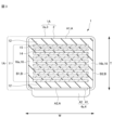
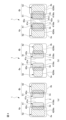
- FIG. 2 is a cross-sectional view of the multilayer ceramic capacitor 1 taken along line II-II shown in FIG. 2 is a cross-sectional view of the multilayer ceramic capacitor 1 taken along line III-III shown in FIG. 4A to 4C are plan views of various shapes of spacers 4 as viewed from the stacking direction. 4A to 4C are plan views of various shapes of spacers 4 as viewed from the stacking direction.
- FIG. 11 is an enlarged cross-sectional view of a portion of the second region 42 when a phenolic resin is used.
- FIG. 11 is an enlarged cross-sectional view of a portion of the second region 42 when an epoxy resin is used.
- FIG. 2 is a flowchart showing a method for manufacturing the multilayer ceramic capacitor 1.
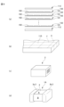
- 3A to 3C are diagrams illustrating a laminate manufacturing step S1, a base electrode layer forming step S2, and a plating layer forming step S3.
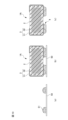
- 13A to 13C are diagrams illustrating a second region forming step in the spacer arrangement step S4.
- a multilayer ceramic capacitor 1 will be described as an embodiment of a multilayer ceramic electronic component of the present invention, but the present invention is not limited thereto.
- the drawings may be drawn in a schematic and simplified manner in order to explain the contents of the invention, and the dimensional ratios of the depicted components or between the components may not match those dimensional ratios described in the specification.
- components described in the specification may be omitted in the drawings, or may be drawn with the number of components omitted.
- FIG. 1 is a schematic perspective view of a multilayer ceramic capacitor 1 according to an embodiment.
- FIG. 2 is a cross-sectional view of the multilayer ceramic capacitor 1 according to an embodiment taken along line II-II in FIG. 1.
- FIG. 3 is a cross-sectional view of the multilayer ceramic capacitor 1 according to an embodiment taken along line III-III in FIG. 1. Note that FIG. 2 is a cross-section parallel to the length direction L and the stacking direction T, and is also referred to as an LT cross-section. Also, FIG. 3 is a cross-section parallel to the width direction W and the stacking direction T, and is also referred to as a WT cross-section.
- the multilayer ceramic capacitor 1 is substantially rectangular and includes a capacitor body 1A having a laminate 2 and a pair of external electrodes 3 provided at both ends of the laminate 2, and a spacer 4 attached to the capacitor body 1A.
- the laminate 2 also includes an inner layer 11 in which a dielectric layer 14 and an internal electrode layer 15 are laminated.
- the terms used to indicate the orientation of the multilayer ceramic capacitor 1 are the length direction L, which is the direction in which the pair of external electrodes 3 are provided in the multilayer ceramic capacitor 1.
- the direction in which the dielectric layers 14 and the internal electrode layers 15 are stacked is the stacking direction T.
- the direction that intersects both the length direction L and the stacking direction T is the width direction W. Note that in this embodiment, the width direction W is perpendicular to both the length direction L and the stacking direction T.
- Outer surface of laminate 2 Among the six outer surfaces of the laminate 2, a pair of outer surfaces facing each other in the stacking direction T is referred to as a first main surface A1 and a second main surface A2, a pair of outer surfaces facing each other in the width direction W is referred to as a first side surface B1 and a second side surface B2, and a pair of outer surfaces facing each other in the length direction L is referred to as a first end surface C1 and a second end surface C2.
- first main surface A1 and the second main surface A2 and to describe them differently when it is not necessary to distinguish between the first main surface A1 and the second main surface A2 and to describe them differently, they will be collectively referred to as a main surface A, when it is not necessary to distinguish between the first side surface B1 and the second side surface B2 and to describe them differently, they will be collectively referred to as a side surface B, and when it is not necessary to distinguish between the first end surface C1 and the second end surface C2 and to describe them differently, they will be collectively referred to as an end surface C.
- the laminate 2 preferably has rounded ridges R1, including the corners.
- the ridges R1 are the intersections of two surfaces of the laminate 2, i.e., the main surface A and the side surface B, the main surface A and the end surface C, or the side surface B and the end surface C.
- the laminate 2 comprises an inner layer portion 11 that forms a capacitance, an outer layer portion 12 that is arranged to sandwich the inner layer portion 11 in the stacking direction T, and a side margin portion 16 that is arranged to sandwich the inner layer portion 11 and the outer layer portion 12 in the width direction W.
- the inner layer portion 11 includes dielectric layers 14 and internal electrode layers 15 alternately stacked along a stacking direction T.
- the dielectric layer 14 is made of a ceramic material, such as a dielectric ceramic containing BaTiO3 as a main component.
- the internal electrode layer 15 includes a plurality of first internal electrode layers 15a and a plurality of second internal electrode layers 15b.
- the first internal electrode layers 15a and the second internal electrode layers 15b are alternately arranged.
- the first internal electrode layer 15a includes a first opposing portion 152a facing the second internal electrode layer 15b, and a first lead portion 151a drawn from the first opposing portion 152a to the first end face C1 side. An end of the first lead portion 151a is exposed to the first end face C1 and is electrically connected to the first external electrode 3a described later.
- the second internal electrode layer 15b includes a second opposing portion 152b facing the first internal electrode layer 15a, and a second lead portion 151b drawn from the second opposing portion 152b to the second end face C2. An end of the second lead portion 151b is electrically connected to the second external electrode 3b described later. Charges are stored in the first opposing portions 152a of the first internal electrode layers 15a and the second opposing portions 152b of the second internal electrode layers 15b.
- the internal electrode layer 15 is preferably formed from a metal material such as nickel (Ni), copper (Cu), silver (Ag), palladium (Pd), a silver-palladium (Ag-Pd) alloy, or gold (Au).
- a metal material such as nickel (Ni), copper (Cu), silver (Ag), palladium (Pd), a silver-palladium (Ag-Pd) alloy, or gold (Au).
- the outer layer portion 12 can be formed of the same material as the dielectric layer 14 of the inner layer portion 11 .
- the multilayer ceramic capacitor 1 includes a first side margin portion 16a that is disposed so as to sandwich the inner layer portion 11 and the outer layer portion 12 in the width direction W and that forms a first side surface B1 of the multilayer ceramic capacitor 1, and a second side margin portion 16b that forms a second side surface B2 of the multilayer ceramic capacitor 1.
- the side margin portion 16 can be formed of the same material as the dielectric layer 14.
- the external electrode 3 includes a first external electrode 3a provided on the first end face C1 and a second external electrode 3b provided on the second end face C2.
- the external electrode 3 covers not only the end face C but also a part of the main face A and the side face B continuing from the end face C.
- the end of the first extension portion 151a of the first internal electrode layer 15a is exposed to the first end face C1 and is electrically connected to the first external electrode 3a.
- the end of the second extension portion 151b of the second internal electrode layer 15b is exposed to the second end face C2 and is electrically connected to the second external electrode 3b.
- the external electrode 3 includes, for example, a base electrode layer 30 and a plating layer 31. It is not necessary for the external electrode 3 to have such a layered structure.
- the external electrode 3 may include a resin electrode layer to relieve stress on the multilayer ceramic capacitor 1.
- the base electrode layer 30 is formed, for example, by applying and baking a conductive paste containing copper (Cu).
- the base electrode layer 30 may also contain glass or ceramic materials.
- the plating layer 31 includes a nickel (Ni) plating layer disposed on the surface of the base electrode layer 30, and a first tin (Sn) plating layer disposed on the surface of the nickel (Ni) plating layer 31a. Note that the configuration of the plating layer 31 is not limited to this.
- the spacer 4 includes a pair of a first spacer 4a and a second spacer 4b.
- the first spacer 4a is disposed on a first end face C1 side in the length direction L on the second main surface A2 side, which is the substrate mounting surface of the capacitor body 1A
- the second spacer 4b is disposed on the other second end face C2 side.
- the substrate mounting surface of the capacitor body 1A is the first side face B1
- the first spacer 4a is disposed on the first end face C1 side in the length direction L on the first side face B1 side, which is the substrate mounting surface of the capacitor body 1A
- the second spacer 4b is disposed on the other second end face C2 side.
- the spacer 4 is disposed on the external electrode 3 of the capacitor body 1A and on the surface of the second main surface A2 of the laminate 2 on which the subsequent external electrode 3 is not disposed.
- the spacer 4 is disposed on the external electrode 3 of the capacitor body 1A and on the surface of the first side surface B1 of the laminate 2 on which the subsequent external electrode 3 is not disposed.
- the external electrode 3 is composed of a base electrode layer 30 and a plating layer 31 covering it, and the spacer 4 is disposed on the surface of the plating layer 31, but the plating layer 31 is not necessarily required, and for example, the spacer 4 may be disposed on the surface of the base electrode layer 30.
- the first region 41 is formed from a material that has a high adhesive strength with the laminate 2.
- the first region 41 is formed from a metal film produced by sputtering, a mixture of a conductive component and a ceramic material, or a synthetic resin, the first region 41 will be more likely to adhere to the surface of the laminate 2, improving the adhesive strength between the capacitor body 1A and the spacer 4.
- the first region can be formed from an insulating resin.
- the insulating resin can be mainly composed of an epoxy resin, which can be combined with a phenolic resin as a hardener.
- Other hardeners that can be used include acid anhydride-based, amine-based, and ester-based hardeners.
- a hardening accelerator may also be added to the epoxy resin.
- the insulating resin may be formed from only a water-repellent treatment agent.
- the second region 42 can contain various components such as metal components and resin components. For example, if the second region 42 contains a large amount of metal components, the ratio of the volume of the metal components to the surface area increases, and the ESR of the multilayer ceramic electronic component decreases. On the other hand, if the second region 42 contains a large amount of resin components, the elasticity of the resin components can relieve stress. When the first region 41 contains a large amount of resin components, it is preferable that the second region 42 contains a large amount of metal components. The first region 41 can improve the mechanical strength and flexural strength, and the second region 42 can relieve the increase in ESR.
- the resin component that forms the second region 42 may be, for example, a resin such as a phenol resin or an epoxy resin.
- FIG. 6 shows an example of the structure of the second region 42 when the second region is formed using phenolic resin.
- FIG. 6 is a partially enlarged cross-sectional view of the internal region of the second region 42.
- the second region 42 shown in FIG. 6 contains either copper (Cu) or nickel (Ni) and tin (Sn) as metal powder.
- the copper (Cu) and nickel (Ni) may be coated with silver (Ag).
- the intermetallic compound formed by adding either copper (Cu) or nickel (Ni) and tin (Sn) is less likely to deform due to heat even when soldering is performed when mounting the multilayer ceramic capacitor 1 on a wiring board, and can reliably maintain the shape of the second region 42.
- the intermetallic compound formed by adding tin (Sn) to an alloy of copper (Cu) and nickel (Ni) is preferable as a component for forming the second region 42.
- Phenolic resin is included in the metal region MP formed by the metal powder.
- the phenolic resin coats the particles of the intermetallic compound and is scattered so as to fill the gaps between the particles.
- the phenolic resin may not completely coat the particles of the intermetallic compound.
- the amount of gas generated during the heat treatment for forming the second region 42 can be reduced, and therefore the voids P in the second region 42 can be reduced.
- the phenolic resin may be exposed on the surface of the second region 42 and cover at least a portion of the surface of the second region 42.
- phenolic resins include novolac-type phenolic resins such as phenol novolac resin, phenol aralkyl resin, cresol novolac resin, tert-butylphenol novolac resin, and nonylphenol novolac resin, resol-type phenolic resin, and polyoxystyrene such as polyparaoxystyrene.
- metal powder MF may be included in the resin region RP formed by the phenolic resin.
- the metal powder MF can inhibit the shrinkage of the phenolic resin, thereby reducing the shrinkage stress caused by the phenolic resin.
- FIG. 7 shows an example of the structure of the second region 42 when the second region is formed using epoxy resin.
- FIG. 7 is a partially enlarged cross-sectional view of the internal region of the second region 42.
- the second region 42 shown in FIG. 7 includes a tin (Sn) region, a resin region RP, a metal region MP containing copper (Cu) or copper (Cu) and nickel (Ni), and a silver (Ag) region.
- the metal region MP is shown as Cu in the figure, but contains either copper (Cu) or a metal containing copper (Cu) and nickel (Ni).
- the metal region MP may also contain tin (Sn).
- the metal containing copper (Cu) and nickel (Ni) may be an alloy of copper (Cu) and nickel (Ni), or may further contain tin (Sn) to form an intermetallic compound.
- tin (Sn) may be contained within the silver (Ag) region.
- the resin region RP also includes those that contain within it a metal region MP that contains copper (Cu) surrounded by tin (Sn) or silver (Ag) or that contains copper (Cu) and nickel (Ni).
- a metal region MP that contains copper (Cu) surrounded by tin (Sn) or silver (Ag) or that contains copper (Cu) and nickel (Ni).
- the metal region MP contains copper (Cu) and nickel (Ni)
- the copper (Cu) and nickel (Ni) may be alloyed, or may further contain tin (Sn) to form an intermetallic compound.
- the composition of the incorporated material is detected as is.
- the different materials forming the first region 41 and the second region 42 do not necessarily mean that the components contained in the first region 41 and the second region 42 are all or partly different, but also include cases where the components are the same but have different contents or compositions.
- the difference in components can be detected, for example, as follows.
- the cross section is polished parallel to the mounting surface of the multilayer ceramic capacitor and to 1/6 of the short side to expose the cross section in the height x long direction.
- the cross section obtained by polishing the cross section is magnified to a total magnification of 50 times using a microscope (BX-51), and photographed with a microscope digital camera (DP22 made by Olympus).
- DP22 microscope digital camera
- photographs can also be taken with a microscope (Axio (registered trademark)-Imager-MAT, made by ZEISS) at a total magnification of 100 to 500 times.
- the first region 41 can cover a part of the laminate 2 and a part of the external electrode 3.
- the edge 3e of the external electrode 3 it is possible to alleviate the stress concentrated at the edge 3e of the external electrode 3, and to improve the flexural strength.
- This arrangement makes it easy to make the thickness of the first region 41 in the stacking direction T smaller than the thickness of the second region in the stacking direction T, and to make the thickness of the first region 41 in the stacking direction T smaller than the thickness of the external electrode 3 in the stacking direction T.
- the thickness of the first region 41 in the stacking direction T By making the thickness of the first region 41 in the stacking direction T smaller, the dimension of the multilayer ceramic capacitor 1 in the direction perpendicular to the mounting surface can be made relatively small, thereby increasing the degree of freedom in the arrangement when mounting the multilayer ceramic capacitor 1.
- the thickness of the first region 41 in the stacking direction T can be found, for example, by the following method.
- the LT cross section is photographed using a microscope (Axio (registered trademark)-Imager-MAT, manufactured by ZEISS) at a total magnification of 100 to 500 times. From the obtained image, the first region is divided into 10 equal parts in the length direction L, and the thickness in the stacking direction T is measured at the center of each of the 10 regions, and the average value of these measurements can be used as the thickness of the first region 41 in the stacking direction T.
- the spacer 4 By arranging the spacer 4 in this manner, it is possible to ensure a sufficient area where the first region 41 is bonded to the laminate 2 and where the second region 42 is bonded to the first region 41, thereby improving the adhesion between the capacitor body 1A and the spacer 4.
- a direction discrimination means can be provided on a part of the spacer 4 or on a part of the capacitor body 1A.
- the direction discrimination means indicates the direction when the multilayer ceramic capacitor is mounted on a wiring board, so that the surface on which the spacer 4 is arranged faces the wiring board.
- a direction discrimination means for example, a means can be used to color the first region 41 or the second region 42 of the spacer 4 in a color different from that of the external electrode 3, a means can be used to print a mark for discriminating the direction, such as a QR code (registered trademark), or a means can be used to provide a recess in part of the laminate 2.
- the first region 41 When the first region 41 is made of an insulating material, the first region 41 may completely cover the second main surface of the laminate 2 that faces the mounting surface, or may continuously cover the area between the first external electrode 3a and the second external electrode 3b that face each other in the length direction L.
- the thickness of the spacer 4 in the stacking direction T is preferably, for example, 50 ⁇ m to 250 ⁇ m.
- the thickness of the spacer 4 in the stacking direction T can be designed appropriately depending on the size of the multilayer ceramic capacitor 1. For example, when the length direction L dimension of the capacitor body 1A is 1.6 mm, the width direction W dimension is 0.8 mm, and the stacking direction T dimension is 0.8 mm, the thickness of the spacer 4 in the stacking direction T is preferably about 160 ⁇ m.
- Figure 5 illustrates two embodiments in which the second region 42 of the spacer 4 has different shapes.
- a recess is provided on the left side surface of the first spacer 4a and the right side surface of the second spacer 4b, making each of them U-shaped
- a recess is provided on the left and right side surfaces of the first spacer 4a and the left and right side surfaces of the second spacer 4b, making each of them H-shaped.
- Fig. 8 is a flow chart illustrating a method for manufacturing the multilayer ceramic capacitor 1.
- the method for manufacturing the multilayer ceramic capacitor 1 includes a laminate manufacturing step S1, a base electrode layer forming step S2, a plating layer forming step S3, and a spacer arranging step S4.
- Fig. 9 is a diagram illustrating the laminate manufacturing step S1, the base electrode layer forming step S2, and the plating layer forming step S3.
- Fig. 10 is a diagram illustrating the step of forming the second region in the spacer arranging step S4.
- a ceramic slurry containing ceramic powder, a binder, and a solvent is formed into a sheet shape on the surface of a carrier film using a die coater, a gravure coater, a microgravure coater, or the like to prepare a laminated ceramic green sheet 101 that will become the dielectric layer 14.
- a conductive paste is printed in stripes on the laminated ceramic green sheet 101 by screen printing, inkjet printing, gravure printing, or the like, and a conductive pattern 102 that will become the internal electrode layer 15 is printed on the surface of the laminated ceramic green sheet 101 to prepare a material sheet 103.
- multiple material sheets 103 are stacked so that the conductive patterns 102 face the same direction and are offset, for example, by half a pitch in the length direction between adjacent material sheets 103. Furthermore, outer layer ceramic green sheets 112 that will become the outer layer 12 are stacked on both sides of the multiple stacked material sheets 103.
- the stacked material sheets 103 and the outer layer ceramic green sheets 112 are pressed together using a hydrostatic press or the like to create the mother block 110 shown in Figure 9(b).
- the mother block 110 is cut along the cutting line X shown in FIG. 9(b) and the cutting line Y that intersects with the cutting line X, and then fired to produce a plurality of laminates 2 shown in FIG. 9(c).
- Base electrode layer formation step S2 Next, a conductive paste containing copper (Cu) is applied to the end faces C of the laminate 2 and baked to form the base electrode layer 30.
- the base electrode layer 30 is formed not only on the end faces C on both sides of the laminate 2 but also on the other end faces C on both sides of the laminate 2.
- the insulating layer 2 is formed so as to extend to the main surface A and the side surface B of the laminate 2 and to cover a part of the end surface C of the main surface A.
- the insulating layer 2 is not limited to this, and may contain other metals and other components.
- two base electrode layers may be provided.
- a plating layer 31 is formed on the surface of the base electrode layer 30 to produce the capacitor body 1A shown in Fig. 9(d) .
- the plating layer 31 can be composed of a nickel (Ni) plating layer and a tin (Sn) plating layer disposed on the surface of the nickel (Ni) plating layer, but is not limited thereto.
- the spacer arrangement step S4 includes the following first region formation step and second region formation step.
- a paste for the first region which is the material for the first region, is applied by, for example, a dispensing method, a printing method such as a squeegee method, or a sputtering method so as to cover a part of the laminate and a part of the external electrodes.
- the first region can be arranged in a desired range by changing the design of the mask, for example, to cover a part of the external electrode or not. By adjusting the amount, the thickness of the first region 41 in the stacking direction T can be adjusted.
- the paste for the first region is heated at a desired temperature to harden it.
- the first region can be formed by firing, and if the paste for the first region contains a resin component, the first region can be formed by thermal hardening.
- a paste 51 for the second region is prepared to be used for forming the second region 42.
- the paste 51 for the second region is, for example, a phenol resin-based paste or an epoxy resin-based paste as described below.
- the second region paste 51 contains metals made of copper (Cu), nickel (Ni), tin (Sn), and silver (Ag), a phenol resin, a solvent, and an additive.
- phenolic resins include novolac-type phenolic resins such as phenol novolac resin, phenol aralkyl resin, cresol novolac resin, tert-butylphenol novolac resin, and nonylphenol novolac resin, resol-type phenolic resin, and polyoxystyrene such as polyparaoxystyrene.
- a holding substrate 50 as shown in FIG. 10 is used.
- a paste 51 for the second region is placed on the holding substrate 50 by a screen printing method, a dispense method or the like.
- the capacitor body 1A is mounted on the upper surface of the holding substrate 50 with the second main surface A2 facing the holding substrate 50.
- the external electrode 3 of the capacitor body 1A and the paste for the second region 51 are aligned, and the paste for the second region 51 is attached to the capacitor body 1A.
- the heating process is carried out.
- the metal in the paste produces an intermetallic compound and the metal region MP is formed
- some of the phenolic resin is taken into the metal region MP and some is expelled from the metal region MP, while hardening, forming a spacer 4 bonded to the capacitor body 1A.
- the capacitor body 1A is separated from the holding substrate 50 together with the spacer 4, resulting in the state shown in FIG. 10(c).
- the manufacturing method is not limited to this, and the second region 42 may be formed by placing the paste for the second region in a desired shape directly on the surface of the capacitor body 1A and performing a heat treatment.
- the paste 51 for the second region contains a metal made of copper and nickel coated with tin (Sn), copper (Cu) coated with silver (Ag), or copper (Cu) coated with silver (Ag) instead of copper (Cu), a resin made of epoxy resin, and a solvent.
- the epoxy resin is a bisphenol A type epoxy resin.
- the solvent is, for example, diethylene glycol monobutyl ether, diethylene glycol monoethyl ether, or diethylene glycol monomethyl ether.
- the bump manufacturing paste 44 does not contain a hardener such as a phenol resin or imidazole.
- the volume ratio of tin (Sn) to the total volume of the metal is between 70% and 90%.
- the volume ratio of metal to resin is between 70% and 90%.
- the process for forming the second region can be the process shown in FIG. 10 above.
- the heat treatment for forming the first region or the second region can be carried out in each of the first region forming process and the second region forming process, but depending on the components of the paste for the first region and the paste for the second region, the heat treatment may be carried out simultaneously.
- the above describes an embodiment of the present invention, but the present invention is not limited to the embodiment, and can be implemented in various forms without departing from the gist of the present invention.
- the present invention includes the following combinations.
- a laminate including an inner layer portion in which dielectric layers and internal electrode layers are alternately laminated, the laminate having two main faces opposing each other in a lamination direction, two end faces opposing each other in a length direction intersecting the lamination direction, and two side faces opposing each other in a width direction intersecting the lamination direction and the length direction;
- Two external electrodes are connected to the internal electrode layers at the two end faces, respectively, and cover the end faces and parts of the two main faces or parts of the two side faces that are adjacent to the end faces;
- two spacers arranged on one of the two main surfaces or one of the two side surfaces of the laminate; the spacer includes a first region covering a portion of the laminate and a second region covering a portion of the external electrode, The first region and the second region are made of different materials.
- ⁇ 2> The multilayer ceramic electronic component according to ⁇ 1>, wherein the first region covers a part of the laminate and a part of the external electrode.
- ⁇ 3> The multilayer ceramic electronic component according to ⁇ 1> or ⁇ 2>, wherein the second region covers a part of the external electrode and a part of the first region.
- ⁇ 4> ⁇ 4> The multilayer ceramic electronic component according to any one of ⁇ 1> to ⁇ 3>, wherein an edge of the first region of the spacer, which is located toward the center of the laminate in the longitudinal direction, is located closer to the center of the laminate than an edge of the second region of the spacer, which is located toward the center of the laminate in the longitudinal direction.
Landscapes
- Engineering & Computer Science (AREA)
- Power Engineering (AREA)
- Microelectronics & Electronic Packaging (AREA)
- Manufacturing & Machinery (AREA)
- Chemical & Material Sciences (AREA)
- Ceramic Engineering (AREA)
- Inorganic Chemistry (AREA)
- Materials Engineering (AREA)
- Fixed Capacitors And Capacitor Manufacturing Machines (AREA)
- Ceramic Capacitors (AREA)
Abstract
コンデンサ本体とスペーサとの固着力が高く、実装した際の耐久性にすぐれた積層セラミックコンデンサを提供すること。 誘電体層14と内部電極層15とが交互に積層された内層部11を含み、積層方向Tに相対する2つの主面A、長さ方向Lに相対する2つの端面Cを備えた積層体2と、 前記2つの端面Cのそれぞれにおいて、前記内部電極層15に接続するとともに、前記端面Cとこれに続けて相対する前記2つの主面Aの一部を被覆する2つの外部電極3と、 前記積層体2の前記2つの主面Aの一方に配置される2つのスペーサ4と、を備え、 前記スペーサ4は、前記積層体2の一部を被覆する第1領域41と、前記外部電極3の一部を被覆する第2領域42と、を含み、 前記第1領域41と前記第2領域42は異なる材料からなる、積層セラミック電子部品1。
Description
本発明は、積層セラミックコンデンサ等の積層セラミック電子部品に関する。
積層セラミックコンデンサなどの積層セラミック電子部品は、携帯電話機等の移動体端末機器又はパーソナルコンピューターなどの各種電子機器に多く利用されている。積層セラミックコンデンサは、誘電体層と内部電極層とを交互に積層した直方体状の積層体と、当該積層体の対向する両端に形成された外部電極とを備える。
積層セラミックコンデンサは、誘電体層と内部電極とが交互に積み重ねられた内層部を有する。そして、その内層部の上部と下部とに外層部としての誘電体層が配置されて直方体状の積層体が形成され、積層体の長手方向の両端面に外部電極が設けられてコンデンサ本体が形成される。
さらに、いわゆる「鳴き」の発生を抑制するために、コンデンサ本体における基板に実装される側に外部電極の一部を覆うように形成されたスペーサを備える積層セラミックコンデンサが知られている。
しかしながら、コンデンサ本体とスペーサとの固着力が弱いと、スペーサが剥離してしまう場合があり、実装した際の耐久性において十分ではなかった。
本発明は、コンデンサ本体とスペーサとの固着力が高く、実装した際の耐久性にすぐれた積層セラミックコンデンサを提供することを目的とする。
本発明者は、積層体の一部を覆う第1領域と、外部電極の一部を覆う第2領域と、を有し、第1領域と第2領域は異なる材料からなるスペーサは、コンデンサ本体との固着力が高く、実装した際の耐久性にすぐれることを見出し、本発明を完成するに至った。
すなわち、本発明は、誘電体層と内部電極層とが交互に積層された内層部を含み、積層方向に相対する2つの主面、前記積層方向に交差する長さ方向に相対する2つの端面、及び、前記積層方向及び前記長さ方向と交差する幅方向に相対する2つの側面を備えた積層体と、
前記2つの端面のそれぞれにおいて、前記内部電極層に接続するとともに、前記端面とこれに続けて相対する前記2つの主面の一部又は前記2つの側面の一部を被覆する2つの外部電極と、
前記積層体の前記2つの主面の一方又は前記2つの側面の一方に配置される2つのスペーサと、を備え、
前記スペーサは、前記積層体の一部を被覆する第1領域と、前記外部電極の一部を被覆する第2領域と、を含み、
前記第1領域と前記第2領域は異なる材料からなる、積層セラミック電子部品である。
前記2つの端面のそれぞれにおいて、前記内部電極層に接続するとともに、前記端面とこれに続けて相対する前記2つの主面の一部又は前記2つの側面の一部を被覆する2つの外部電極と、
前記積層体の前記2つの主面の一方又は前記2つの側面の一方に配置される2つのスペーサと、を備え、
前記スペーサは、前記積層体の一部を被覆する第1領域と、前記外部電極の一部を被覆する第2領域と、を含み、
前記第1領域と前記第2領域は異なる材料からなる、積層セラミック電子部品である。
本発明によれば、コンデンサ本体とスペーサとの固着力を高めることができるため、実装した際の耐久性にすぐれた積層セラミックコンデンサを提供することが可能となる。
以下、本発明の積層セラミック電子部品の実施形態として積層セラミックコンデンサ1について説明するが、本発明がこれに限定されることはない。また、図面は、発明の内容を説明するため、模式的に簡略化して描画している場合があり、描画された構成要素または構成要素間の寸法の比率が、明細書に記載されたそれらの寸法の比率と一致していない場合がある。また、明細書に記載されている構成要素が、図面において省略されている場合や、個数を省略して描画されている場合などがある。
図1は、実施形態の積層セラミックコンデンサ1の概略斜視図である。図2は、実施形態の積層セラミックコンデンサ1の図1におけるII-II線に沿った断面図である。図3は、実施形態の積層セラミックコンデンサ1の図1におけるIII-III線に沿った断面図である。なお、図2は長さ方向Lと積層方向Tに平行な断面であり、LT断面とも称される。また、図3は、幅方向Wと積層方向Tに平行な断面であり、WT断面とも称される。
積層セラミックコンデンサ1は、略直方体形状で、積層体2及び積層体2の両端に設けられた一対の外部電極3を備えるコンデンサ本体1Aと、コンデンサ本体1Aに取り付けられたスペーサ4と、を備える。また、積層体2は、誘電体層14と内部電極層15とを積層した内層部11を含む。
以下の説明において、積層セラミックコンデンサ1の向きを表わす用語として、積層セラミックコンデンサ1において、一対の外部電極3が設けられている方向を長さ方向Lとする。誘電体層14と内部電極層15とが積層されている方向を積層方向Tとする。長さ方向L及び積層方向Tのいずれにも交差する方向を幅方向Wとする。なお、実施形態においては、幅方向Wは長さ方向L及び積層方向Tのいずれにも直交している。
(積層体2の外表面)
また、積層体2の6つの外表面のうち、積層方向Tに相対する一対の外表面を第1主面A1と第2主面A2とし、幅方向Wに相対する一対の外表面を第1側面B1と第2側面B2とし、長さ方向Lに相対する一対の外表面を第1端面C1と第2端面C2とする。なお、第1主面A1と第2主面A2とを特に区別して説明する必要のない場合、まとめて主面Aとし、第1側面B1と第2側面B2とを特に区別して説明する必要のない場合、まとめて側面Bとし、第1端面C1と第2端面C2とを特に区別して説明する必要のない場合、まとめて端面Cとして説明する。
また、積層体2の6つの外表面のうち、積層方向Tに相対する一対の外表面を第1主面A1と第2主面A2とし、幅方向Wに相対する一対の外表面を第1側面B1と第2側面B2とし、長さ方向Lに相対する一対の外表面を第1端面C1と第2端面C2とする。なお、第1主面A1と第2主面A2とを特に区別して説明する必要のない場合、まとめて主面Aとし、第1側面B1と第2側面B2とを特に区別して説明する必要のない場合、まとめて側面Bとし、第1端面C1と第2端面C2とを特に区別して説明する必要のない場合、まとめて端面Cとして説明する。
積層体2は、角部を含む稜線部R1に丸みがつけられていることが好ましい。稜線部R1は、積層体2の2面、すなわち主面Aと側面B、主面Aと端面C、または、側面Bと端面Cが交わる部分である。
(積層体2)
積層体2は、静電容量を形成する内層部11と、内層部11を積層方向Tから挟み込むように配置される外層部12と、内層部11と外層部12を幅方向Wから挟み込むように配置されるサイドマージン部16と、を備える。
積層体2は、静電容量を形成する内層部11と、内層部11を積層方向Tから挟み込むように配置される外層部12と、内層部11と外層部12を幅方向Wから挟み込むように配置されるサイドマージン部16と、を備える。
(内層部11)
内層部11は、積層方向Tに沿って交互に積層された誘電体層14と内部電極層15とを含む。
内層部11は、積層方向Tに沿って交互に積層された誘電体層14と内部電極層15とを含む。
(誘電体層14)
誘電体層14は、セラミック材料で製造されている。セラミック材料としては、例えば、BaTiO3を主成分とする誘電体セラミックが用いられる。
誘電体層14は、セラミック材料で製造されている。セラミック材料としては、例えば、BaTiO3を主成分とする誘電体セラミックが用いられる。
(内部電極層15)
内部電極層15は、複数の第1内部電極層15aと、複数の第2内部電極層15bとを備える。第1内部電極層15aと第2内部電極層15bとは、交互に配置されている。第1内部電極層15aは、第2内部電極層15bと対向する第1対向部152aと、第1対向部152aから第1端面C1側に引き出された第1引き出し部151aとを備える。第1引き出し部151aの端部は、第1端面C1に露出し、後述の第1外部電極3aに電気的に接続されている。第2内部電極層15bは、第1内部電極層15aと対向する第2対向部152bと、第2対向部152bから第2端面C2に引き出された第2引き出し部151bとを備える。第2引き出し部151bの端部は、後述の第2外部電極3bに電気的に接続されている。第1内部電極層15aの第1対向部152aと、第2内部電極層15bの第2対向部152bとに電荷が蓄積される。
内部電極層15は、複数の第1内部電極層15aと、複数の第2内部電極層15bとを備える。第1内部電極層15aと第2内部電極層15bとは、交互に配置されている。第1内部電極層15aは、第2内部電極層15bと対向する第1対向部152aと、第1対向部152aから第1端面C1側に引き出された第1引き出し部151aとを備える。第1引き出し部151aの端部は、第1端面C1に露出し、後述の第1外部電極3aに電気的に接続されている。第2内部電極層15bは、第1内部電極層15aと対向する第2対向部152bと、第2対向部152bから第2端面C2に引き出された第2引き出し部151bとを備える。第2引き出し部151bの端部は、後述の第2外部電極3bに電気的に接続されている。第1内部電極層15aの第1対向部152aと、第2内部電極層15bの第2対向部152bとに電荷が蓄積される。
内部電極層15は、例えばニッケル(Ni)、銅(Cu)、銀(Ag)、パラジウム(Pd)、銀-パラジウム(Ag-Pd)合金、金(Au)等に代表される金属材料により形成されていることが好ましい。
(外層部12)
外層部12は、内層部11の誘電体層14と同じ材料で形成することができる。
外層部12は、内層部11の誘電体層14と同じ材料で形成することができる。
(サイドマージン部16)
内層部11と外層部12を幅方向Wから挟み込むように配置され、積層セラミックコンデンサ1の第1側面B1を形成する第1サイドマージン部16aと、積層セラミックコンデンサ1の第2側面B2を形成する第2サイドマージン部16bと、を備える。サイドマージン部16は、誘電体層14と同じ材料で形成することができる。
内層部11と外層部12を幅方向Wから挟み込むように配置され、積層セラミックコンデンサ1の第1側面B1を形成する第1サイドマージン部16aと、積層セラミックコンデンサ1の第2側面B2を形成する第2サイドマージン部16bと、を備える。サイドマージン部16は、誘電体層14と同じ材料で形成することができる。
(外部電極3)
外部電極3は、第1端面C1に設けられた第1外部電極3aと、第2端面C2に設けられた第2外部電極3bとを備える。外部電極3は、端面Cだけでなく、端面Cに続く主面A及び側面Bの一部も覆っている。
外部電極3は、第1端面C1に設けられた第1外部電極3aと、第2端面C2に設けられた第2外部電極3bとを備える。外部電極3は、端面Cだけでなく、端面Cに続く主面A及び側面Bの一部も覆っている。
上述のように、第1内部電極層15aの第1引き出し部151aの端部は第1端面C1に露出し、第1外部電極3aに電気的に接続されている。また、第2内部電極層15bの第2引き出し部151bの端部は第2端面C2に露出し、第2外部電極3bに電気的に接続されている。これにより、第1外部電極3aと第2外部電極3bとの間は、複数のコンデンサ要素が電気的に並列に接続された構造となっている。
また、外部電極3は、例えば下地電極層30とめっき層31を含む。なお、外部電極3が、このような層状構造であることは、必ずしも必要でない。これに加え、積層セラミックコンデンサ1にかかる応力を緩和するために樹脂電極層を含んでいてもよい。
下地電極層30は、例えば、銅(Cu)を含む導電性ペーストを塗布、焼き付けることにより形成される。また、下地電極層30はガラスやセラミック材料を含んでもよい。
めっき層31は、下地電極層30の表面に配置されたニッケル(Ni)めっき層と、かかるニッケル(Ni)めっき層31aの表面に配置された第1錫(Sn)めっき層とを含む。なお、めっき層31の構成は、これに限定されるものではない。
(スペーサ4)
スペーサ4は、一対の第1スペーサ4aと第2スペーサ4bとを備える。第1スペーサ4aは、コンデンサ本体1Aの基板実装面である第2主面A2側における、長さ方向Lの一方の第1端面C1側に配置され、第2スペーサ4bは、他方の第2端面C2側に配置されている。コンデンサ本体1Aの基板実装面が第1側面B1である場合、第1スペーサ4aは、コンデンサ本体1Aの基板実装面である第1側面B1側における、長さ方向Lの一方の第1端面C1側に配置され、第2スペーサ4bは、他方の第2端面C2側に配置される。
スペーサ4は、一対の第1スペーサ4aと第2スペーサ4bとを備える。第1スペーサ4aは、コンデンサ本体1Aの基板実装面である第2主面A2側における、長さ方向Lの一方の第1端面C1側に配置され、第2スペーサ4bは、他方の第2端面C2側に配置されている。コンデンサ本体1Aの基板実装面が第1側面B1である場合、第1スペーサ4aは、コンデンサ本体1Aの基板実装面である第1側面B1側における、長さ方向Lの一方の第1端面C1側に配置され、第2スペーサ4bは、他方の第2端面C2側に配置される。
スペーサ4は、コンデンサ本体1Aの外部電極3と、これに続く外部電極3が配置されていない積層体2の第2主面A2の表面上に配置されている。コンデンサ本体1Aの基板実装面が第1側面B1である場合、スペーサ4は、コンデンサ本体1Aの外部電極3と、これに続く外部電極3が配置されていない積層体2の第1側面B1の表面上に配置される。
実施形態においては、外部電極3を下地電極層30とこれを被覆するめっき層31とにより構成し、スペーサ4は、めっき層31の表面に配置する態様を示したが、必ずしも、めっき層31は必要ではなく、例えば、下地電極層30の表面にスペーサ4を配置してもよい。
スペーサ4は、積層体2の一部を被覆する第1領域41と、外部電極3の一部を被覆する第2領域42と、を含み、第1領域41と第2領域42は異なる材料により形成される。
第1領域41は、積層体2との固着力が高い材料により形成される。例えば、第1領域41をスパッタリングによる金属膜、導電成分とセラミック材料の混合物、あるいは合成樹脂により形成すると、積層体2の表面に第1領域41が密着し易くなるため、コンデンサ本体1Aとスペーサ4との固着力を向上させることができる。
第1領域は、絶縁性樹脂によって形成することができる。絶縁性樹脂は、例えば、エポキシ樹脂を主成分とし、これにフェノール樹脂を硬化剤として組み合わせることができる。その他の硬化剤としては、酸無水物系、アミン系、及びエステル系等の硬化剤を用いることができる。エポキシ樹脂には、さらに硬化促進剤を添加してもよい。絶縁性樹脂は、撥水処理剤のみで形成されていてもよい。
第2領域42は、金属成分や樹脂成分など種々の成分を含有することができるが、例えば、金属成分を多く含むと、金属成分の表面積に対する体積の割合が増加するため、積層セラミック電子部品のESRが低下する。一方、樹脂成分を多く含むと、樹脂成分による弾性によって応力を緩和することができる。第1領域41が樹脂成分を多く含んでいる場合、第2の領域42は金属成分を多く含有することが好ましい。第1領域41によって機械強度やたわみ強度を向上することができ、かつ、第2領域42によってESRの増加を緩和することができる。
第2領域42を形成する樹脂成分としては、例えば、フェノール樹脂、エポキシ樹脂等の樹脂を用いることができる。
フェノール樹脂を用いて第2領域を形成した場合の第2領域42の構造の一例を図6に示す。図6は、第2領域42の内部領域の断面の一部拡大図である。
図6に示す第2領域42は、金属粉として、銅(Cu)またはニッケル(Ni)のいずれかと錫(Sn)を含む。銅(Cu)とニッケル(Ni)は、銀(Ag)で被覆してもよい。銅(Cu)またはニッケル(Ni)のいずれかと錫(Sn)を加えて形成される金属間化合物は、積層セラミックコンデンサ1を配線基板に実装する際、はんだ付けを行う場合にも、熱による変形が生じることが少なく、確実に第2領域42の形状を維持することができる。特に、銅(Cu)とニッケル(Ni)との合金に錫(Sn)を加えて形成される金属間化合物は、第2領域42を形成する成分として好ましい。
金属粉が形成する金属領域MP中に、フェノール樹脂が含まれる。フェノール樹脂は、金属間化合物の粒子を被覆するとともに、粒子間の隙間を埋めるように点在する。フェノール樹脂は、金属間化合物の粒子を完全に被覆しない状態であってもよい。また、フェノール樹脂を用いることにより、第2領域42を形成する際の加熱処理において、ガスの発生量を少なくすることができるため、第2領域42内の空隙Pを減らすことができる。フェノール樹脂は、第2領域42の表面に表出し第2領域42の表面の少なくとも一部を被覆してもよい。フェノール樹脂が第2領域42の表面を被覆することにより、第2領域の表面の平滑性が向上し、スペーサ4の機械的強度を高めることができる。
フェノール樹脂は、例えば、フェノールノボラック樹脂、フェノールアラルキル樹脂、クレゾールノボラック樹脂、tert-ブチルフェノールノボラック樹脂、ノニルフェノールノボラック樹脂などのノボラック型フェノール樹脂、レゾール型フェノール樹脂、ポリパラオキシスチレンなどのポリオキシスチレンなどが挙げられる。
図4に示すように、フェノール樹脂が形成する樹脂領域RP中に金属粉MFを含んでもよい。フェノール樹脂の収縮を金属粉MFによって阻害し、フェノール樹脂による収縮応力を緩和することができる。
エポキシ樹脂を用いて第2領域を形成した場合の第2領域42の構造の一例を図7に示す。図7は、第2領域42の内部領域の断面の一部拡大図である。
図7に示す第2領域42は、錫(Sn)領域と、樹脂領域RPと、銅(Cu)、又は、銅(Cu)とニッケル(Ni)とを含む金属領域MPと、銀(Ag)領域と、を含む。金属領域MPは、図中Cuとして表すが、銅(Cu)、または、銅(Cu)とニッケル(Ni)とを含有する金属のどちらかを含有している。また、金属領域MPは錫(Sn)を含んでもよい。なお、銅(Cu)とニッケル(Ni)とを含有する金属は、銅(Cu)とニッケル(Ni)とが合金化していてもよいし、さらに錫(Sn)を含み金属間化合物となっていてもよい。なお、銀(Ag)領域内に錫(Sn)を含んでいてもよい。錫(Sn)の内部に含まれるこれらの領域は、WDXやEDXの解析により検出可能である。
また、樹脂領域RPは、内部に、錫(Sn)、銀(Ag)で周囲が覆われた銅(Cu)もしくは銅(Cu)及びニッケル(Ni)を含む金属領域MPを含有するものを含む。なお、金属領域MPが銅(Cu)およびニッケル(Ni)を含む場合、銅(Cu)とニッケル(Ni)は合金化していてもよく、さらに錫(Sn)を含み金属間化合物となっていてもよい。特に樹脂領域RP内では、材料として抱合された組成がそのまま検出される。
第1領域41と第2領域42を形成する異なる材料とは、第1領域41と第2領域42に含有される成分が、全てあるいは一部異なる場合に限らず、成分が共通しても含有量が異なる場合や組成が異なる場合などもこれに含まれる。
成分の違いは、例えば、以下のようにして検出することができる。
積層セラミックコンデンサの実装面に平行、かつ、短手方向の1/6まで断面研磨を行い、高さ×長手方向の断面を露出させる。断面研磨して得られた断面において、例えば、顕微鏡(BX-51)で総合倍率50倍に拡大し、顕微鏡用デジタルカメラ(オリンパス製のDP22)で撮影する。また、これに限らず、顕微鏡(Axio(登録商標)‐Imager‐MAT、ZEISS製)を使用して総合倍率100~500倍にて撮影することも出来る。
積層セラミックコンデンサの実装面に平行、かつ、短手方向の1/6まで断面研磨を行い、高さ×長手方向の断面を露出させる。断面研磨して得られた断面において、例えば、顕微鏡(BX-51)で総合倍率50倍に拡大し、顕微鏡用デジタルカメラ(オリンパス製のDP22)で撮影する。また、これに限らず、顕微鏡(Axio(登録商標)‐Imager‐MAT、ZEISS製)を使用して総合倍率100~500倍にて撮影することも出来る。
図4は、積層方向Tからみたスペーサ4の平面図である。図4には、第1領域41と第2領域42の形状と大きさが異なる3つの実施形態を例示する。
図4に示すように、第1領域41は、積層体2の一部と外部電極3の一部を被覆することができる。第1領域41が、積層体2の一部と、これに連続して外部電極3の縁端部3eを覆うことにより、外部電極3の縁端部3eに集中する応力を緩和させることができ、たわみ強度を向上させることができる。また、外部電極3の縁端部3eからの水分侵入を抑制することができる。
第2領域42が、外部電極3の一部と第1領域41の一部を被覆することにより第1領域41の少なくとも一部が、積層体2と第2領域42との間に配置されることが好ましい。
このような配置により、第1領域41の積層方向Tの厚みを第2領域の積層方向Tの厚みより小さくするとともに、第1領域41の積層方向Tの厚みを外部電極3の積層方向Tの厚みより小さくすることが容易となり、第1領域41の積層方向Tの厚みを小さくすることで、積層セラミックコンデンサ1の実装面に垂直な方向の寸法を比較的小さく形成することができるため、積層セラミックコンデンサ1を実装する際の配置において自由度を増すことができる。
第1領域41の積層方向Tの厚みは、例えば、以下の方法により求めることができる。まず、積層セラミックコンデンサ1の幅方向Wの長さ1/6に相当する位置まで研磨し、長さ方向Lと積層方向Tに平行なLT断面を露出させる。LT断面を顕微鏡(Axio(登録商標)‐Imager‐MAT、ZEISS製)を使用して総合倍率100~500倍にて撮影する。得られた画像から、第1領域を長さ方向Lに10等分し、10個の各領域の中心において、積層方向Tの厚みを計測し、これらの平均値をもって第1領域41の積層方向Tの厚みとすることができる。
図4(a)と図4(b)に示すように、第1スペーサ4aあるいは第2スペーサ4bのいずれか一方を見たとき、長さ方向Lにおいて積層体2の中央側に位置する第1領域41の縁辺41eは、長さ方向Lにおいて積層体2の中央側に位置する第2領域42の縁辺42eより、積層体2の中央側に位置するようにスペーサ4を配置することができる。また、図4(b)に示すように、第1領域41の幅方向Wの縁辺41Weは、第2領域42の幅方向Wの縁辺42Weより幅方向Wにおいて外側に位置するようにスペーサ4を配置してもよい。
このようにスペーサ4を配置することによって、第1領域41が積層体2へ接合する面積と、第2領域42が第1領域41へ接合する面積を十分に確保することが可能となり、コンデンサ本体1Aとスペーサ4との固着力を向上させることができる。
スペーサ4の一部や、コンデンサ本体1Aの一部に方向判別手段を設けることができる。方向判別手段は、積層セラミックコンデンサを配線基板に実装する際、スペーサ4を配置した面を配線基板に対向するように方向を示すものである。方向判別手段の備えるためには、例えば、外部電極3とは異なる色でスペーサ4の第1領域41または第2領域42を着色する手段や、QRコード(登録商標)のような方向を判別するためのマークを印刷する手段や、積層体2の一部に凹部を設けるなどの手段を施すことができる。
第1領域41が絶縁性の材料からなる場合、第1領域41は、実装面と対向する積層体2の第2主面を完全に被覆してもよく、長さ方向Lにおいて対向している第1外部電極3aと第2外部電極3bの間を連続的に被覆してもよい。
スペーサ4の積層方向Tの厚みは、例えば、50μm~250μmであることが好ましい。スペーサ4の積層方向Tの厚みは、積層セラミックコンデンサ1の大きさにより適宜設計することが可能であり、例えば、コンデンサ本体1Aの長さ方向Lの寸法が1.6mm、幅方向Wの寸法が0.8mm、積層方向Tの寸法が0.8mmのとき、スペーサ4の積層方向Tの厚みは、160μm程度であることが好ましい。
図5は、スペーサ4の第2領域42の形状が異なる2つの実施形態を例示している。図5(a)に示す形態は、第1スペーサ4aの左側面と第2スペーサ4bの右側面に凹部を設けて、それぞれコの字状とし、図5(b)に示す形態は、第1スペーサ4aの左右の側面と第2スペーサ4bの左右の側面に凹部を設け、それぞれH字状としている。
このように、スペーサ4の側面に凹部を形成することにより、実装する際に必要となる配線基板との接触面積を十分確保しながら、溶融した余分のはんだを凹部に収容し、はんだがコンデンサ本体1Aの実装面から垂直な方向に高く濡れ上がることを防ぐことができるため、鳴きの発生をより確実に抑えることができる。
(積層セラミックコンデンサ1の製造方法)
図8は、積層セラミックコンデンサ1の製造方法を説明するフローチャートである。積層セラミックコンデンサ1の製造方法は、積層体製造工程S1と、下地電極層形成工程S2と、めっき層形成工程S3と、スペーサ配置工程S4と、を含む。図9は、積層体製造工程S1と、下地電極層形成工程S2と、めっき層形成工程S3とを説明する図である。図10は、スペーサ配置工程S4における第2領域を形成する工程を説明する図である。
図8は、積層セラミックコンデンサ1の製造方法を説明するフローチャートである。積層セラミックコンデンサ1の製造方法は、積層体製造工程S1と、下地電極層形成工程S2と、めっき層形成工程S3と、スペーサ配置工程S4と、を含む。図9は、積層体製造工程S1と、下地電極層形成工程S2と、めっき層形成工程S3とを説明する図である。図10は、スペーサ配置工程S4における第2領域を形成する工程を説明する図である。
(積層体製造工程S1)
セラミックス粉末、バインダ及び溶剤を含むセラミックスラリーをキャリアフィルムの表面においてダイコータ、グラビアコータ、マイクログラビアコータ等を用いてシート状に成形して誘電体層14となる積層用セラミックグリーンシート101を作成する。次いで、積層用セラミックグリーンシート101に導電体ペーストをスクリーン印刷、インクジェット印刷、グラビア印刷等によって帯状に印刷し、積層用セラミックグリーンシート101の表面に内部電極層15となる導電パターン102を印刷して素材シート103を作成する。
セラミックス粉末、バインダ及び溶剤を含むセラミックスラリーをキャリアフィルムの表面においてダイコータ、グラビアコータ、マイクログラビアコータ等を用いてシート状に成形して誘電体層14となる積層用セラミックグリーンシート101を作成する。次いで、積層用セラミックグリーンシート101に導電体ペーストをスクリーン印刷、インクジェット印刷、グラビア印刷等によって帯状に印刷し、積層用セラミックグリーンシート101の表面に内部電極層15となる導電パターン102を印刷して素材シート103を作成する。
続いて、図9(a)に示すように、導電パターン102が同一の方向を向き且つ導電パターン102が隣り合う素材シート103間において長さ方向において、例えば、半ピッチずつずれた状態になるように、複数の素材シート103を積み重ねる。さらに、複数枚積層された素材シート103の両側にそれぞれ、外層部12となる外層部用セラミックグリーンシート112を積み重ねる。
積み重ねた複数の素材シート103と外層部用セラミックグリーンシート112とを静水圧プレスなどで圧着し、図9(b)に示すマザーブロック110を作成する。
次いで、マザーブロック110を、図9(b)に示す切断線X及び切断線Xと交差する切断線Yに沿って切断し、焼成することによって、図9(c)に示す積層体2を複数製造する。
(下地電極層形成工程S2)
続いて、積層体2の端面Cに、銅(Cu)を含む導電性ペーストを塗布、焼き付けることにより下地電極層30を形成する。下地電極層30は、積層体2両側の端面Cのみならず、積層体2の主面A及び側面B側まで延びて、主面Aの端面C側の一部も覆うように形成する。しかし、これに限定されず、他の金属や他の成分を含んでいてもよく、下地電極層を二層設けてもよい。
続いて、積層体2の端面Cに、銅(Cu)を含む導電性ペーストを塗布、焼き付けることにより下地電極層30を形成する。下地電極層30は、積層体2両側の端面Cのみならず、積層体2の主面A及び側面B側まで延びて、主面Aの端面C側の一部も覆うように形成する。しかし、これに限定されず、他の金属や他の成分を含んでいてもよく、下地電極層を二層設けてもよい。
(めっき層形成工程S3)
次いで、下地電極層30の表面にめっき層31を形成し、図9(d)に示すコンデンサ本体1Aを製造する。めっき層31は、ニッケル(Ni)めっき層と、ニッケル(Ni)めっき層の表面に配置された錫(Sn)めっき層により構成することができるが、これに限定されるものではない。
次いで、下地電極層30の表面にめっき層31を形成し、図9(d)に示すコンデンサ本体1Aを製造する。めっき層31は、ニッケル(Ni)めっき層と、ニッケル(Ni)めっき層の表面に配置された錫(Sn)めっき層により構成することができるが、これに限定されるものではない。
(スペーサ配置工程S4)
スペーサ配置工程S4は、以下の第1領域形成工程と第2領域形成工程からなる。
スペーサ配置工程S4は、以下の第1領域形成工程と第2領域形成工程からなる。
(第1領域形成工程)
積層体の一部と外部電極の一部を被覆するように、第1領域の材料となる第1領域用ペーストを、たとえば、ディスペンス法、スキージ法などの印刷法、あるいはスパッタリング法等により塗布する。このとき、外部電極の一部を被覆するか否かなど、たとえば、マスクの設計を変更するなどして任意の範囲に第1領域を配置することができる。また、第1領域用ペーストの量を調整することで、第1領域41の積層方向Tの厚みを調整することができる。
積層体の一部と外部電極の一部を被覆するように、第1領域の材料となる第1領域用ペーストを、たとえば、ディスペンス法、スキージ法などの印刷法、あるいはスパッタリング法等により塗布する。このとき、外部電極の一部を被覆するか否かなど、たとえば、マスクの設計を変更するなどして任意の範囲に第1領域を配置することができる。また、第1領域用ペーストの量を調整することで、第1領域41の積層方向Tの厚みを調整することができる。
その後、第1領域用ペーストを任意の温度で加熱し硬化させる。例えば、第1領域用ペーストに金属成分が含有される場合は、焼成により、また、第1領域用ペーストに樹脂成分が含有される場合は、熱硬化により、第1領域を形成することができる。
(第2領域形成工程)
第2領域42の形成に用いる、第2領域用ペースト51を用意する。第2領域用ペースト51としては、例えば、以下のフェノール樹脂系とエポキシ樹脂系がある。
第2領域42の形成に用いる、第2領域用ペースト51を用意する。第2領域用ペースト51としては、例えば、以下のフェノール樹脂系とエポキシ樹脂系がある。
(フェノール樹脂系)
第2領域用ペースト51は、銅(Cu)、ニッケル(Ni)、錫(Sn)、銀(Ag)からなる金属と、フェノール樹脂と、溶剤と、添加剤と、を含む。
第2領域用ペースト51は、銅(Cu)、ニッケル(Ni)、錫(Sn)、銀(Ag)からなる金属と、フェノール樹脂と、溶剤と、添加剤と、を含む。
フェノール樹脂は、例えば、フェノールノボラック樹脂、フェノールアラルキル樹脂、クレゾールノボラック樹脂、tert-ブチルフェノールノボラック樹脂、ノニルフェノールノボラック樹脂などのノボラック型フェノール樹脂、レゾール型フェノール樹脂、ポリパラオキシスチレンなどのポリオキシスチレンなどが挙げられる。
第2領域42の形成には、例えば、図10に示すような保持基板50を用いる。
保持基板50の上に、第2領域用ペースト51をスクリーン印刷法またはディスペンス法等により配置する。
保持基板50の上に、第2領域用ペースト51をスクリーン印刷法またはディスペンス法等により配置する。
次に、コンデンサ本体1Aを図10(b)に示すように、第2主面A2側が保持基板50に対向する姿勢で保持基板50の上面に搭載する。このとき、コンデンサ本体1Aの外部電極3と第2領域用ペースト51とが位置合わせされ、第2領域用ペースト51がコンデンサ本体1Aに付着する。
この状態で、加熱工程を実施する。ペースト中の少なくとも一部の金属が金属間化合物を生成し金属領域MPが形成する際、フェノール樹脂の一部は金属領域MPの中に取り込まれ、一部は金属領域MPから排出されながら、硬化し、コンデンサ本体1Aに接合したスペーサ4が形成される。
その後、コンデンサ本体1Aがスペーサ4とともに、保持基板50から分離され、図10(c)の状態となる。なお、このような製造方法に限らず、コンデンサ本体1Aの表面上に直接所望の形に第2領域用ペーストを配置し、加熱処理を行い、第2領域42を形成してもよい。
(エポキシ樹脂系)
第2領域用ペースト51は、錫(Sn)、銀(Ag)で被覆された銅(Cu)、もしくは銅(Cu)に替わって銀(Ag)で被覆された、銅とニッケルからなる金属と、エポキシ樹脂製の樹脂と、溶剤と、を含む。
第2領域用ペースト51は、錫(Sn)、銀(Ag)で被覆された銅(Cu)、もしくは銅(Cu)に替わって銀(Ag)で被覆された、銅とニッケルからなる金属と、エポキシ樹脂製の樹脂と、溶剤と、を含む。
エポキシ樹脂は、ビスフェノールA型エポキシ樹脂である。溶剤は、例えばジエチレングリコールモノブチルエーテル、ジエチレングリコールモノエチルエーテルまたはジエチレングリコールモノメチルエーテルである。そして、バンプ製造用ペースト44は、フェノール樹脂やイミダゾールなどの硬化剤を含まない。
金属の全体体積に対して錫(Sn)の体積比率は70%以上90%以下である。樹脂に対する、金属の体積比率は、70%以上90%以下である。
第2領域の形成工程は、上述の図10に示す工程を採用することができる。
第1領域あるいは第2領域を形成するための熱処理は、上述のように、第1領域形成工程と第2領域形成工程のそれぞれにおいて行うことができるが、第1領域用ペーストと第2領域用ペーストの成分によっては、同時に熱処理を実施しても良い。
以上、本発明の実施形態について説明したが、本発明は実施形態に限定されるものではなく、本発明の要旨を逸脱しない範囲において種々の態様で実施することが可能である。本発明は以下の組み合わせを含む。
<1>
誘電体層と内部電極層とが交互に積層された内層部を含み、積層方向に相対する2つの主面、前記積層方向に交差する長さ方向に相対する2つの端面、及び、前記積層方向及び前記長さ方向と交差する幅方向に相対する2つの側面を備えた積層体と、
前記2つの端面のそれぞれにおいて、前記内部電極層に接続するとともに、前記端面とこれに続けて相対する前記2つの主面の一部又は前記2つの側面の一部を被覆する2つの外部電極と、
前記積層体の前記2つの主面の一方又は前記2つの側面の一方に配置される2つのスペーサと、を備え、
前記スペーサは、前記積層体の一部を被覆する第1領域と、前記外部電極の一部を被覆する第2領域と、を含み、
前記第1領域と前記第2領域は異なる材料からなる、積層セラミック電子部品。
<2>
前記第1領域は、前記積層体の一部と前記外部電極の一部を被覆する、<1>記載の積層セラミック電子部品。
<3>
前記第2領域は、前記外部電極の一部と前記第1領域の一部を被覆する、<1>又は<2>記載の積層セラミック電子部品。
<4>
前記長さ方向において前記積層体の中央側に位置する前記スペーサの前記第1領域の縁辺は、前記長さ方向において前記積層体の中央側に位置する前記スペーサの前記第2領域の縁辺より、前記積層体の中央側に位置する<1>乃至<3>のいずれかに記載の積層セラミック電子部品。
誘電体層と内部電極層とが交互に積層された内層部を含み、積層方向に相対する2つの主面、前記積層方向に交差する長さ方向に相対する2つの端面、及び、前記積層方向及び前記長さ方向と交差する幅方向に相対する2つの側面を備えた積層体と、
前記2つの端面のそれぞれにおいて、前記内部電極層に接続するとともに、前記端面とこれに続けて相対する前記2つの主面の一部又は前記2つの側面の一部を被覆する2つの外部電極と、
前記積層体の前記2つの主面の一方又は前記2つの側面の一方に配置される2つのスペーサと、を備え、
前記スペーサは、前記積層体の一部を被覆する第1領域と、前記外部電極の一部を被覆する第2領域と、を含み、
前記第1領域と前記第2領域は異なる材料からなる、積層セラミック電子部品。
<2>
前記第1領域は、前記積層体の一部と前記外部電極の一部を被覆する、<1>記載の積層セラミック電子部品。
<3>
前記第2領域は、前記外部電極の一部と前記第1領域の一部を被覆する、<1>又は<2>記載の積層セラミック電子部品。
<4>
前記長さ方向において前記積層体の中央側に位置する前記スペーサの前記第1領域の縁辺は、前記長さ方向において前記積層体の中央側に位置する前記スペーサの前記第2領域の縁辺より、前記積層体の中央側に位置する<1>乃至<3>のいずれかに記載の積層セラミック電子部品。
A 主面
A1 第1主面
A2 第2主面
B 側面
C 端面
MF 金属粉
MP 金属領域
P 空隙
RP 樹脂領域
1 積層セラミックコンデンサ(積層セラミック電子部品)
1A コンデンサ本体
2 積層体
3 外部電極
4 スペーサ
4a 第1スペーサ
4b 第2スペーサ
11 内層部
12 外層部
14 誘電体層
15 内部電極層
16 サイドマージン部
30 下地電極層
31 めっき層
41 第1領域
42 第2領域
50 保持基板
51 第2領域用ペースト
A1 第1主面
A2 第2主面
B 側面
C 端面
MF 金属粉
MP 金属領域
P 空隙
RP 樹脂領域
1 積層セラミックコンデンサ(積層セラミック電子部品)
1A コンデンサ本体
2 積層体
3 外部電極
4 スペーサ
4a 第1スペーサ
4b 第2スペーサ
11 内層部
12 外層部
14 誘電体層
15 内部電極層
16 サイドマージン部
30 下地電極層
31 めっき層
41 第1領域
42 第2領域
50 保持基板
51 第2領域用ペースト
Claims (4)
- 誘電体層と内部電極層とが交互に積層された内層部を含み、積層方向に相対する2つの主面、前記積層方向に交差する長さ方向に相対する2つの端面、及び、前記積層方向及び前記長さ方向と交差する幅方向に相対する2つの側面を備えた積層体と、
前記2つの端面のそれぞれにおいて、前記内部電極層に接続するとともに、前記端面とこれに続けて相対する前記2つの主面の一部又は前記2つの側面の一部を被覆する2つの外部電極と、
前記積層体の前記2つの主面の一方又は前記2つの側面の一方に配置される2つのスペーサと、を備え、
前記スペーサは、前記積層体の一部を被覆する第1領域と、前記外部電極の一部を被覆する第2領域と、を含み、
前記第1領域と前記第2領域は異なる材料からなる、積層セラミック電子部品。 - 前記第1領域は、前記積層体の一部と前記外部電極の一部を被覆する、請求項1記載の積層セラミック電子部品。
- 前記第2領域は、前記外部電極の一部と前記第1領域の一部を被覆する、請求項1又は2記載の積層セラミック電子部品。
- 前記長さ方向において前記積層体の中央側に位置する前記スペーサの前記第1領域の縁辺は、前記長さ方向において前記積層体の中央側に位置する前記スペーサの前記第2領域の縁辺より、前記積層体の中央側に位置する請求項1乃至3のいずれかに記載の積層セラミック電子部品。
Priority Applications (2)
| Application Number | Priority Date | Filing Date | Title |
|---|---|---|---|
| KR1020257036695A KR20250168612A (ko) | 2023-06-08 | 2024-05-23 | 적층 세라믹 전자부품 |
| US19/367,918 US20260058062A1 (en) | 2023-06-08 | 2025-10-24 | Multilayer ceramic electronic component |
Applications Claiming Priority (2)
| Application Number | Priority Date | Filing Date | Title |
|---|---|---|---|
| JP2023094856 | 2023-06-08 | ||
| JP2023-094856 | 2023-06-08 |
Related Child Applications (1)
| Application Number | Title | Priority Date | Filing Date |
|---|---|---|---|
| US19/367,918 Continuation US20260058062A1 (en) | 2023-06-08 | 2025-10-24 | Multilayer ceramic electronic component |
Publications (1)
| Publication Number | Publication Date |
|---|---|
| WO2024252946A1 true WO2024252946A1 (ja) | 2024-12-12 |
Family
ID=93795875
Family Applications (1)
| Application Number | Title | Priority Date | Filing Date |
|---|---|---|---|
| PCT/JP2024/019023 Ceased WO2024252946A1 (ja) | 2023-06-08 | 2024-05-23 | 積層セラミック電子部品 |
Country Status (3)
| Country | Link |
|---|---|
| US (1) | US20260058062A1 (ja) |
| KR (1) | KR20250168612A (ja) |
| WO (1) | WO2024252946A1 (ja) |
Citations (1)
| Publication number | Priority date | Publication date | Assignee | Title |
|---|---|---|---|---|
| JP2022099069A (ja) * | 2020-12-22 | 2022-07-04 | 株式会社村田製作所 | 積層セラミックコンデンサ及び積層セラミックコンデンサの製造方法 |
Family Cites Families (1)
| Publication number | Priority date | Publication date | Assignee | Title |
|---|---|---|---|---|
| KR101630037B1 (ko) | 2014-05-08 | 2016-06-13 | 삼성전기주식회사 | 적층 세라믹 커패시터, 어레이형 적층 세라믹 커패시터, 그 제조 방법 및 그 실장 기판 |
-
2024
- 2024-05-23 WO PCT/JP2024/019023 patent/WO2024252946A1/ja not_active Ceased
- 2024-05-23 KR KR1020257036695A patent/KR20250168612A/ko active Pending
-
2025
- 2025-10-24 US US19/367,918 patent/US20260058062A1/en active Pending
Patent Citations (1)
| Publication number | Priority date | Publication date | Assignee | Title |
|---|---|---|---|---|
| JP2022099069A (ja) * | 2020-12-22 | 2022-07-04 | 株式会社村田製作所 | 積層セラミックコンデンサ及び積層セラミックコンデンサの製造方法 |
Also Published As
| Publication number | Publication date |
|---|---|
| US20260058062A1 (en) | 2026-02-26 |
| KR20250168612A (ko) | 2025-12-02 |
Similar Documents
| Publication | Publication Date | Title |
|---|---|---|
| CN118248463A (zh) | 层叠陶瓷电容器 | |
| JP2024099773A (ja) | 電子部品、回路基板および電子部品の製造方法 | |
| JP6672786B2 (ja) | 積層セラミック電子部品 | |
| US12237111B2 (en) | Multilayer ceramic capacitor | |
| US20260024699A1 (en) | Multilayer ceramic electronic component | |
| JP7647920B2 (ja) | 積層セラミックコンデンサ及びバンプ製造用ペースト | |
| JP7690995B2 (ja) | 積層セラミックコンデンサ及びバンプ製造用ペースト | |
| US12469644B2 (en) | Multilayer ceramic capacitor and bump-producing paste | |
| US20260058062A1 (en) | Multilayer ceramic electronic component | |
| US20260011504A1 (en) | Multilayer ceramic electronic component | |
| US20260018337A1 (en) | Multilayer ceramic electronic component | |
| JP7861797B2 (ja) | 積層セラミックコンデンサ及び積層セラミックコンデンサのバンプ製造用ペースト | |
| US20260011502A1 (en) | Laminated ceramic electronic component | |
| WO2025163972A1 (ja) | 積層セラミック電子部品 | |
| US20250329496A1 (en) | Multilayer ceramic capacitor | |
| WO2025163971A1 (ja) | 積層セラミック電子部品 | |
| WO2025163973A1 (ja) | 積層セラミック電子部品 | |
| US20260128229A1 (en) | Multilayer ceramic capacitor | |
| WO2024203711A1 (ja) | 積層セラミック電子部品 | |
| WO2024202403A1 (ja) | 積層セラミック電子部品 | |
| WO2026009777A1 (ja) | 積層セラミック電子部品 | |
| WO2026009776A1 (ja) | 積層セラミック電子部品 | |
| WO2025046969A1 (ja) | 積層セラミック電子部品 | |
| WO2025234429A1 (ja) | 積層セラミック電子部品 | |
| WO2025225548A1 (ja) | 積層セラミック電子部品 |
Legal Events
| Date | Code | Title | Description |
|---|---|---|---|
| 121 | Ep: the epo has been informed by wipo that ep was designated in this application |
Ref document number: 24819178 Country of ref document: EP Kind code of ref document: A1 |
|
| ENP | Entry into the national phase |
Ref document number: 1020257036695 Country of ref document: KR Free format text: ST27 STATUS EVENT CODE: A-0-1-A10-A15-NAP-PA0105 (AS PROVIDED BY THE NATIONAL OFFICE) |
|
| WWE | Wipo information: entry into national phase |
Ref document number: KR1020257036695 Country of ref document: KR |
|
| NENP | Non-entry into the national phase |
Ref country code: DE |