WO2024252916A1 - 脈波測定装置 - Google Patents
脈波測定装置 Download PDFInfo
- Publication number
- WO2024252916A1 WO2024252916A1 PCT/JP2024/018617 JP2024018617W WO2024252916A1 WO 2024252916 A1 WO2024252916 A1 WO 2024252916A1 JP 2024018617 W JP2024018617 W JP 2024018617W WO 2024252916 A1 WO2024252916 A1 WO 2024252916A1
- Authority
- WO
- WIPO (PCT)
- Prior art keywords
- pulse wave
- strain
- measuring device
- wave sensor
- pivot
- Prior art date
- Legal status (The legal status is an assumption and is not a legal conclusion. Google has not performed a legal analysis and makes no representation as to the accuracy of the status listed.)
- Ceased
Links
Images








Classifications
-
- A—HUMAN NECESSITIES
- A61—MEDICAL OR VETERINARY SCIENCE; HYGIENE
- A61B—DIAGNOSIS; SURGERY; IDENTIFICATION
- A61B5/00—Measuring for diagnostic purposes; Identification of persons
- A61B5/02—Detecting, measuring or recording for evaluating the cardiovascular system, e.g. pulse, heart rate, blood pressure or blood flow
- A61B5/024—Measuring pulse rate or heart rate
- A61B5/02416—Measuring pulse rate or heart rate using photoplethysmograph signals, e.g. generated by infrared radiation
- A61B5/02427—Details of sensor
-
- A—HUMAN NECESSITIES
- A61—MEDICAL OR VETERINARY SCIENCE; HYGIENE
- A61B—DIAGNOSIS; SURGERY; IDENTIFICATION
- A61B5/00—Measuring for diagnostic purposes; Identification of persons
- A61B5/02—Detecting, measuring or recording for evaluating the cardiovascular system, e.g. pulse, heart rate, blood pressure or blood flow
-
- A—HUMAN NECESSITIES
- A61—MEDICAL OR VETERINARY SCIENCE; HYGIENE
- A61B—DIAGNOSIS; SURGERY; IDENTIFICATION
- A61B5/00—Measuring for diagnostic purposes; Identification of persons
- A61B5/02—Detecting, measuring or recording for evaluating the cardiovascular system, e.g. pulse, heart rate, blood pressure or blood flow
- A61B5/021—Measuring pressure in heart or blood vessels
- A61B5/02108—Measuring pressure in heart or blood vessels from analysis of pulse wave characteristics
-
- A—HUMAN NECESSITIES
- A61—MEDICAL OR VETERINARY SCIENCE; HYGIENE
- A61B—DIAGNOSIS; SURGERY; IDENTIFICATION
- A61B5/00—Measuring for diagnostic purposes; Identification of persons
- A61B5/02—Detecting, measuring or recording for evaluating the cardiovascular system, e.g. pulse, heart rate, blood pressure or blood flow
- A61B5/024—Measuring pulse rate or heart rate
- A61B5/02438—Measuring pulse rate or heart rate with portable devices, e.g. worn by the patient
-
- A—HUMAN NECESSITIES
- A61—MEDICAL OR VETERINARY SCIENCE; HYGIENE
- A61B—DIAGNOSIS; SURGERY; IDENTIFICATION
- A61B5/00—Measuring for diagnostic purposes; Identification of persons
- A61B5/02—Detecting, measuring or recording for evaluating the cardiovascular system, e.g. pulse, heart rate, blood pressure or blood flow
- A61B5/024—Measuring pulse rate or heart rate
- A61B5/02444—Details of sensor
-
- A—HUMAN NECESSITIES
- A61—MEDICAL OR VETERINARY SCIENCE; HYGIENE
- A61B—DIAGNOSIS; SURGERY; IDENTIFICATION
- A61B5/00—Measuring for diagnostic purposes; Identification of persons
- A61B5/68—Arrangements of detecting, measuring or recording means, e.g. sensors, in relation to patient
- A61B5/6801—Arrangements of detecting, measuring or recording means, e.g. sensors, in relation to patient specially adapted to be attached to or worn on the body surface
- A61B5/6802—Sensor mounted on worn items
- A61B5/681—Wristwatch-type devices
-
- A—HUMAN NECESSITIES
- A61—MEDICAL OR VETERINARY SCIENCE; HYGIENE
- A61B—DIAGNOSIS; SURGERY; IDENTIFICATION
- A61B5/00—Measuring for diagnostic purposes; Identification of persons
- A61B5/68—Arrangements of detecting, measuring or recording means, e.g. sensors, in relation to patient
- A61B5/6801—Arrangements of detecting, measuring or recording means, e.g. sensors, in relation to patient specially adapted to be attached to or worn on the body surface
- A61B5/6813—Specially adapted to be attached to a specific body part
- A61B5/6824—Arm or wrist
-
- A—HUMAN NECESSITIES
- A61—MEDICAL OR VETERINARY SCIENCE; HYGIENE
- A61B—DIAGNOSIS; SURGERY; IDENTIFICATION
- A61B2562/00—Details of sensors; Constructional details of sensor housings or probes; Accessories for sensors
- A61B2562/02—Details of sensors specially adapted for in-vivo measurements
- A61B2562/0261—Strain gauges
Definitions
- the present invention relates to a pulse wave measuring device.
- Pulse wave measuring devices equipped with a pulse wave sensor that detects pulse waves generated when the heart pumps blood are known. Such pulse wave measuring devices are configured to be worn, for example, on the wrist of a subject (see, for example, Patent Document 1).
- a pulse wave measuring device using a pulse wave sensor needs to detect minute signals, it is preferable to position the detection surface of the pulse wave sensor approximately parallel to the subject's artery in order to improve measurement accuracy.
- the present invention has been made in consideration of the above points, and aims to provide a pulse wave measuring device that can adjust the angle of the detection surface of the pulse wave sensor to follow the artery.
- a pulse wave measuring device includes a cylindrical portion, a housing, a flexure body provided on one side of the housing, and an opposing portion provided on the other side of the housing.
- the pulse wave sensor is held inside the cylindrical portion so that the flexure body is exposed from one axial end side of the cylindrical portion, a lid portion fixed to the other axial end side of the cylindrical portion, and a wearing portion connected to the outside of the cylindrical portion and can be worn by a subject.
- a first surface of the facing portion and a second surface of the lid portion face each other.
- a pivot portion is provided on one of the first surface and the second surface, and a recess into which the pivot portion can be inserted is opened on the other of the first surface and the second surface. When the pivot portion and the recess come into contact with each other, the pulse wave sensor can swing around the contact portion between the pivot portion and the recess as a fulcrum.
- the disclosed technology makes it possible to provide a pulse wave measuring device that can adjust the angle of the detection surface of the pulse wave sensor to follow the artery.
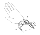
- FIG. 1 is a perspective view (part 1) illustrating a pulse wave measuring device according to a first embodiment
- FIG. 2 is a second perspective view illustrating the pulse wave measuring device according to the first embodiment
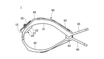
- 1 is a side view illustrating a pulse wave measuring device according to a first embodiment.
- FIG. 4 is a perspective view illustrating a first bending member.
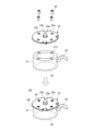
- FIG. 2 is an exploded perspective view illustrating a pulse wave sensor.
- 5A and 5B are diagrams illustrating the positional relationship between a cylindrical portion and a pulse wave sensor.
- 13 is a diagram (part 1) illustrating the positional relationship between the cylindrical portion, the pulse wave sensor, and the cover portion.
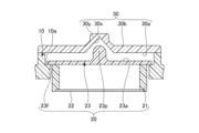
- FIG. FIG. 2 is a diagram (part 2) illustrating the positional relationship between the cylindrical portion, the pulse wave sensor, and the cover portion.
- FIG. 11A to 11C are diagrams illustrating the movement of a pulse wave sensor when the pulse wave sensor comes into contact with a subject.
- 1 is a plan view illustrating a pulse wave sensor according to a first embodiment.
- FIG. 1 is a cross-sectional view illustrating a pulse wave sensor according to a first embodiment. This is an example of a bridge circuit.
- FIG. 2 is a plan view illustrating the strain gauge according to the first embodiment.
- FIG. 1 is a cross-sectional view (part 1) illustrating a strain gauge according to a first embodiment.
- FIG. 2 is a cross-sectional view (part 2) illustrating the strain gauge according to the first embodiment.
- FIG. 1 is a first diagram for explaining a biasing member.
- FIG. 2 is a second diagram for explaining the urging member;
- Fig. 1 is a perspective view (part 1) illustrating the pulse wave measuring device according to the first embodiment, and shows a schematic diagram of the pulse wave measuring device being worn on a subject's wrist.
- Fig. 2 is a perspective view (part 2) illustrating the pulse wave measuring device according to the first embodiment.
- Fig. 3 is a side view illustrating the pulse wave measuring device according to the first embodiment.
- the pulse wave measuring device 1 is a wearable device that can be worn by a subject, and mainly comprises a cylindrical portion 10, a pulse wave sensor 20, a cover portion 30, and a wearing portion 40.
- the tubular portion 10 is a member that holds the pulse wave sensor 20 inside.
- the tubular portion 10 is, for example, cylindrical with both ends open.
- the pulse wave sensor 20 includes a housing 21 and a strain generator 22 provided on one side of the housing 21, and is held inside the tubular portion 10 so that the strain generator 22 is exposed from one axial end side of the tubular portion 10.
- the cover portion 30 is fixed to the other axial end side of the tubular portion 10.
- the attachment portion 40 is connected to the outside of the tubular portion 10.
- the attachment portion 40 is configured to be wearable by the subject.
- the attachment section 40 has a first curved member 41 and a second curved member 42 that are curved in opposite directions and face each other so that it can be attached to the wrist of the subject.
- the first curved member 41 and the second curved member 42 are biased by a biasing member 43 that is bent into a substantially V-shape, and are supported by a swing shaft 44 so that they can transition between a closed state and an open state.
- the first curved member 41 and the second curved member 42 can be made of, for example, resin, etc.
- the biasing member 43 can be made of, for example, metal, etc.
- a lid member 48 is provided on the first curved member 41. The lid member 48 will be described later.
- the tubular portion 10 is disposed at one end of the first bending member 41 in the longitudinal direction, and the swing shaft 44 is disposed at the other end of the first bending member 41 in the longitudinal direction.
- the tubular portion 10 may be formed integrally with the first bending member 41, or may be a separate piece joined thereto.
- the swing shaft 44 may be formed integrally with the first bending member 41, or may be a separate piece joined thereto.
- a first operating unit 45 is provided on the opposite side of the oscillating shaft 44 of the first bending member 41 from the cylindrical portion 10.
- the first operating unit 45 may be formed integrally with the first bending member 41, or may be a separate piece joined to it.
- a second operating unit 46 is provided on the opposite side of the oscillating shaft 44 of the second bending member 42 from the cylindrical portion 10.
- the second operating unit 46 may be formed integrally with the second bending member 42, or may be a separate piece joined to it.
- the subject or an assistant assisting the subject pinches the first operating part 45 and the second operating part 46 and brings them close to each other. This opens the cylindrical part 10 sides of the first bending member 41 and the second bending member 42, allowing the pulse wave measuring device 1 to be put on the subject.
- the pulse wave measuring device 1 is attached to the subject's wrist by the attachment part 40 so that the pulse wave sensor 20 is positioned near the subject's radial artery.
- a pulse wave is a waveform that represents changes in the volume of blood vessels that occur when the heart pumps blood, and the pulse wave measuring device 1 can monitor changes in the volume of blood vessels.
- FIG. 4 is a perspective view for explaining the first curved member, and shows the state in which the cover member 48 is removed from the pulse wave measuring device 1.
- the first curved member 41 may have a component placement area 47 arranged between one end side and the other end side in the longitudinal direction. In the component placement area 47, for example, components that contribute to the detection of pulse waves are placed.
- a wiring board 51 and a battery 52 are exemplified as components that contribute to the detection of pulse waves.
- the wiring board 51 and the battery 52 are electrically connected via wire 53.
- the pulse wave sensor 20 is electrically connected to the wiring board 51 via wire 25.
- a cover member 48 that protects the components is provided on the component placement area 47.
- the wiring board 51 may be mounted with, for example, an amplifier circuit that amplifies the output of the strain gauge 100, an AD converter that converts the output of the amplifier circuit into a digital signal, a semiconductor for signal processing that processes the digital signal, and a semiconductor for wireless communication that transmits the results of the signal processing to the outside.
- a connector may be disposed in the attachment part 40, or a cable may be extended from the attachment part 40.
- FIG. 5 is an exploded perspective view illustrating a pulse wave sensor.
- the pulse wave sensor 20 includes, for example, a housing 21, a strain body 22 provided on one side of the housing 21, and an opposing portion 23 provided on the other side of the housing 21.
- the housing 21 is, for example, a cylindrical member with both ends open.
- the housing 21 can be formed, for example, from metal, resin, etc.
- the flexure body 22 is generally disk-shaped and is fixed to the housing 21 with adhesive or the like so as to cover one side of the housing 21. As described below, the flexure body 22 is a portion in which, for example, a strain gauge is disposed and which detects the pulse wave. A detailed example of the structure of the pulse wave sensor 20 including the flexure body 22 will be described later.
- the facing portion 23 is generally disk-shaped and is fixed to the housing 21 so as to close the other side of the housing 21.
- the facing portion 23 has, for example, a through hole 23x, and is screwed into a groove 21x provided in the housing 21 by a screw 24 inserted into the through hole 23x.
- the facing portion 23 faces the strain body 22 through the space inside the housing 21.
- the mutually facing surfaces of the facing portion 23 and the strain body 22 are, for example, parallel to each other.
- the opposing portion 23 has a first surface 23a, which is the surface opposite to the surface facing the strain body 22.
- the first surface 23a of the opposing portion 23 is, for example, a flat surface.
- a pivot portion 23p that protrudes on the side opposite the strain body 22 is provided at approximately the center of the first surface 23a of the opposing portion 23.
- the pivot portion 23p is, for example, a substantially cylindrical member.
- the central axis of the pivot portion 23p is, for example, perpendicular to the first surface 23a of the opposing portion 23.
- the facing portion 23 has, for example, a flange portion 23f that protrudes from the outer surface of the housing 21 outward in the radial direction of the housing 21.
- the flange portion 23f is, for example, ring-shaped.
- the facing portion 23 may have one or more cutout portions 23y that can be used for preventing rotation, etc.
- the cutout portions 23y are, for example, recessed from the outer periphery of the facing portion 23 toward the center.
- the opposing portion 23 can be made of, for example, metal or resin.
- the pivot portion 23p may be formed integrally with the other portions of the opposing portion 23, or may be a separate piece joined together.
- the pulse wave sensor 20 may have a wire 25 that inputs and outputs electrical signals between the inside and outside of the housing 21. Inside the wire 25, multiple wires that are insulated from each other may be arranged. One end of each of the multiple wires is electrically connected to an electrode of a strain gauge, which will be described later.
- the pulse wave sensor 20 may have a flexible substrate or the like instead of the wire 25.
- one or more wiring boards may be fixed to the inside surface of the housing 21, and a pair of electrodes of the strain gauge may be electrically connected to this wiring board with thin wires. This wiring board may then be electrically connected to the wire 25. With this structure, it becomes difficult for the force from the wire 25 to be transmitted to the strain body 22, improving the accuracy of pulse wave detection.
- Figure 6 is a diagram explaining the positional relationship between the tubular portion and the pulse wave sensor.
- the inner surface of the tubular portion 10 has, for example, a step surface 10a that protrudes toward the axis (toward the center of the tubular portion 10).
- the step surface 10a is, for example, perpendicular to the axial direction of the tubular portion 10.
- the step surface 10a is, for example, ring-shaped.
- the inner surface of the cylindrical portion 10 has, for example, a positioning portion 10b that protrudes toward the shaft side.
- the positioning portion 10b is provided above the step surface 10a.
- two positioning portions 10b are provided so as to face each other.
- Each positioning portion 10b is provided with a groove 10x.
- the pulse wave sensor 20 is held inside the tubular portion 10 with the cutout portion 23y aligned with the positioning portion 10b.
- the pulse wave sensor 20 is not fixed to the tubular portion 10, and has a gap that allows it to move relative to the tubular portion 10.
- the flange portion 23f is in contact with the step surface 10a.
- the pulse wave sensor 20 may be held inside the cylindrical portion 10, the wire 25 may be electrically connected to the wiring board 51, and then the cover member 48 may be fixed onto the component placement area 47.
- the cover member 48 may be screwed into the groove 41x provided in the first curved member 41, for example, by a screw 49.
- Figure 7 is a diagram (part 1) explaining the positional relationship between the tubular portion, the pulse wave sensor, and the lid portion.
- the lid portion 30 has a through hole 30z.
- the lid portion 30 is fixed to the other axial end side of the tubular portion 10 by, for example, screwing into a groove 10x provided in the positioning portion 10b with a screw 32 inserted through the through hole 30z.
- FIG. 8 is a diagram (part 2) explaining the positional relationship between the cylindrical portion, the pulse wave sensor, and the lid portion, and is a partial cross-sectional view showing the cylindrical portion 10, the pulse wave sensor 20, and the lid portion 30.
- the lid portion 30 has a second surface 30a and a third surface 30b opposite the second surface 30a.
- the second surface 30a and the third surface 30b are, for example, parallel to each other.
- a recess 30x that opens toward the second surface 30a is provided in the approximate center of the second surface 30a of the lid portion 30.
- the inner surface of the recess 30x is, for example, a curved surface that is inclined with respect to the axial direction of the tubular portion 10. In a cross-sectional view, the inner surface of the recess 30x may be partially or entirely curved.
- the recess 30x is, for example, conical or truncated conical.
- the recess 30x may be cylindrical with a diameter larger than that of the pivot portion 23p. From the viewpoint of reducing the play between the pivot portion 23p and the recess 30x and facilitating centering, it is preferable that the inner surface of the recess 30x is a single curved surface that is inclined with respect to the axial direction of the cylindrical portion 10, such as a conical or truncated conical shape.
- the lid 30 may have a protrusion 30y that protrudes from approximately the center of the third surface 30b toward the opposite side to the second surface 30a.
- the recess 30x may be positioned so as to overlap with the protrusion 30y when viewed in the axial direction of the tubular portion 10 (the up-down direction in FIG. 8), and a portion of the recess 30x may be positioned within the protrusion 30y. In this way, the lid 30 can be partially thinned.
- the recess 30x side of the pivot portion 23p is, for example, dome-shaped.
- a dome shape is one in which the height is greatest near the central axis, based on the first surface 23a, and decreases toward the periphery.
- the tip side of the pivot portion 23p may be part of a spherical surface or part of an aspherical surface.
- the flange portion 23f of the opposing portion 23 is disposed between the step surface 10a of the cylindrical portion 10 and the second surface 30a of the lid portion 30. With this structure, the flange portion 23f acts as a stopper that prevents the pulse wave sensor 20 from falling downward from the cylindrical portion 10.
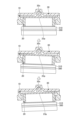
- FIG. 9 is a diagram explaining the movement of the pulse wave sensor when it comes into contact with a subject.
- the attachment part 40 of the pulse wave measuring device 1 is attached to the subject.
- 300 is a schematic diagram of the subject's radial artery.
- the strain body 22 of the pulse wave sensor 20 comes into contact with the skin 310 on the subject's radial artery 300, and the pulse wave sensor 20 is pushed up toward the cover part 30, and the pivot part 23p comes into contact with the recessed part 30x.
- the pivot part 23p and the recessed part 30x are in line contact, for example. This reduces the play between the pivot part 23p and the recessed part 30x, making centering easier.
- this is not limited to this, and the pivot part 23p and the recessed part 30x may be in point contact or surface contact.
- the pulse wave measuring device 1 when the attachment part 40 is not attached to the subject, the pulse wave measuring device 1 is in a first state in which the pivot part 23p and the recess 30x are not in contact (see FIG. 8). Then, when the attachment part 40 is attached to the subject, it switches to a second state in which the pivot part 23p and the recess 30x are in contact (see FIG. 9).
- the pulse wave sensor 20 can swing in a 360-degree direction with the contact point between the pivot portion 23p and the recessed portion 30x as the fulcrum.
- the detection surface of the strain body 22 of the pulse wave sensor 20 can be tilted at any angle along the subject's radial artery 300.
- the angle of the detection surface of the strain body 22 of the pulse wave sensor 20 allows the angle of the detection surface of the strain body 22 of the pulse wave sensor 20 to follow the radial artery 300 of the subject, so that the detection surface of the strain body 22 can be brought into contact with the radial artery 300 of the subject at an appropriate angle.
- the detection surface of the strain body 22 of the pulse wave sensor 20 can be positioned approximately parallel to the radial artery 300 of the subject. As a result, it becomes possible to detect minute pulse wave signals, improving the accuracy of pulse wave measurement.
- the pulse wave sensor 20 can be easily positioned on the radial artery by operating the first operating unit 45 and the second operating unit 46 to transition between the open state and the closed state multiple times and fine-tune the position of the pulse wave sensor 20. At this time, it is preferable to monitor the output signal of the pulse wave sensor 20 and find the position where the amplitude of the output signal is as large as possible.
- a component placement area 47 is provided in the free space of the first curved member 41, and the components that contribute to detecting pulse waves are placed in the component placement area 47, thereby realizing a compact pulse wave detection device equipped with the necessary components.
- the pulse wave measuring device 1 is provided with a biasing member 43, which allows for appropriate pressure to be applied to the subject's radial artery.
- Pulse wave sensor a pulse wave sensor having a plurality of strain gauges is shown as an example of the pulse wave sensor 20.
- the components of the pulse wave sensor 20 duplicated descriptions of those parts that have already been described will be omitted.
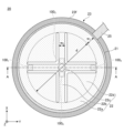
- FIG. 10 is a plan view illustrating a pulse wave sensor according to the first embodiment.
- FIG. 11 is a cross-sectional view illustrating a pulse wave sensor according to the first embodiment, showing a cross section along line A-A in FIG. 10.
- the pulse wave sensor 20 has a housing 21, a strain generating body 22, a facing portion 23, a wire 25, and a plurality of strain gauges (strain gauges 1001 , 1002 , 1003 , 1004 ).
- the facing portion 23 and the wire 25 are as described above. Note that, unless there is a particular need to distinguish between them, the strain gauges 1001 , 1002 , 1003 , 1004 may be collectively referred to as strain gauge 100.
- the strain body 22 has a base portion 22a, a beam portion 22b, a load portion 22c, and an extension portion 22d.
- the strain body 22 is flat.
- the strain body 22 has a first main surface 22m and a second main surface 22n located on the opposite side to the first main surface 22m.
- the material of the strain body 22 may be, for example, metal, ceramic, glass, etc. Examples of metals used as the material of the strain body 22 include SUS (stainless steel), copper, aluminum, etc.
- the strain body 22 may be formed as a single unit, for example, by a press processing method.
- the thickness t of the strain body 22 excluding the load portion 22c is constant.
- the thickness t may be, for example, 0.03 mm or more and 0.3 mm or less.
- the side of the pulse wave sensor 20 on which the load portion 22c of the flexure body 22 is provided is referred to as the "upper side", and the side on which the load portion 22c of the flexure body 22 is not provided is referred to as the "lower side".
- the surface located on the upper side of each part is referred to as the "upper surface”, and the surface located on the lower side of each part is referred to as the "lower surface”.
- the pulse wave sensor 20 can also be used upside down.
- the pulse wave sensor 20 can also be positioned at any angle.
- a planar view refers to viewing an object in a normal direction from the top to the bottom of the first main surface 22m of the flexure body 22.
- a planar shape refers to the shape of the object when viewed in the normal direction.
- the housing 21 is the part that holds the strain body 22.
- the housing 21 can be made of, for example, metal or resin.
- the base 22a is a circular frame-shaped (ring-shaped) region outside the circular dashed line shown in Fig. 10.
- the region inside the circular dashed line may be referred to as a circular opening.
- the base 22a of the flexure body 22 has a circular opening.
- the width w1 of the base 22a is, for example, 1 mm or more and 5 mm or less.
- the inner diameter d of the base 22a (i.e., the diameter of the circular opening) is, for example, 10 mm or more and 15 mm or less.
- the beam portion 22b is provided so as to bridge the inside of the base portion 22a.
- the beam portion 22b has, for example, two beams that cross in a cross shape in a plan view, and the area where the two beams cross includes the center of the circular opening.
- one beam that constitutes the cross has the X direction as its longitudinal direction
- the other beam that constitutes the cross has the Y direction as its longitudinal direction
- the two are perpendicular to each other.
- Each of the two perpendicular beams is preferably located inside the inner diameter d (diameter of the circular opening) of the base portion 22a and is as long as possible. In other words, it is preferable that the length of each beam is approximately equal to the diameter of the circular opening.
- the width w2 other than the area where the beams cross is constant, for example, 1 mm or more and 5 mm or less. It is not essential that the width w2 is constant, but it is preferable that the width w2 is constant in that the strain can be detected linearly.
- the load portion 22c is provided on the beam portion 22b.
- the load portion 22c is provided, for example, in the area where the two beams that make up the beam portion 22b intersect.
- the load portion 22c protrudes from the upper surface of the beam portion 22b.
- the amount of protrusion of the load portion 22c based on the upper surface of the beam portion 22b is, for example, about 0.1 mm.
- the beam portion 22b is flexible, and elastically deforms when a load is applied to the load portion 22c.
- the upper surface of the beam portion 22b is part of the first main surface 22m of the strain generating body 22.
- the four extensions 22d are fan-shaped portions that extend from the inside of the base 22a toward the beam 22b in a plan view. A gap of about 1 mm is provided between each extension 22d and the beam 22b. The extensions 22d do not contribute to the sensing of the pulse wave sensor 20, so they do not need to be provided.
- the output signal of the pulse wave sensor 20 is generated based on the outputs of a plurality of strain gauges.
- the pulse wave sensor 20 has a pair of strain gauges 100-1 and 100-2 arranged on a beam extending in the Y direction on the second main surface 22n of the strain body 22, facing each other across the load portion 22c in a plan view.
- the pulse wave sensor 20 has another pair of strain gauges 100-3 and 100-4 arranged on a beam extending in the X direction intersecting the beam on which the pair of strain gauges 100-1 and 100-2 are arranged, facing each other across the load portion 22c in a plan view.
- the strain gauges 100-1 and 100-2 detect the compressive strain of the strain body 22 that occurs in the beam extending in the Y direction when the load portion 22c is pressed.
- the strain gauges 100-3 and 100-4 detect the tensile strain of the strain body 22 that occurs in the beam extending in the X direction when the load portion 22c is pressed.
- the distance between the strain gauges 100-1 and 100-2 that detect the compressive strain is wider than the distance between the strain gauges 100-3 and 100-4 that detect the tensile strain.
- the strain gauges 100 1 to 100 4 are connected to form each side of a bridge circuit, and the output signal of the pulse wave sensor 20 (a signal indicating a pulse wave) can be generated by the bridge circuit.
- Fig. 12 is an example of a bridge circuit. In the bridge circuit shown in Fig. 12, the strain gauge 100 1 forms the upper left side. The strain gauge 100 2 forms the lower right side. The strain gauge 100 3 forms the upper right side. The strain gauge 100 4 forms the lower left side.
- a DC voltage E is supplied between the connection between the upper left and lower left edges and the connection between the upper right and lower right edges. This allows an analog voltage output signal S1 to be obtained between the connection between the upper left and upper right edges and the connection between the lower left and lower right edges.
- the wiring pattern that constitutes the bridge circuit can be provided, for example, on a wiring board 51.
- the pulse wave sensor 20 when the load portion 22c comes into contact with the subject's radial artery, a load is applied to the load portion 22c in accordance with the subject's pulse wave, causing the beam portion 22b to elastically deform, and the resistance value of the resistor in the strain gauge 100 changes.
- the pulse wave sensor 20 can detect the pulse wave based on the change in the resistance value of the resistor in the strain gauge 100 that accompanies the deformation of the beam portion 22b.
- the pulse wave is detected as a periodic voltage change from the bridge circuit as an output signal S1.
- the pulse wave sensor 20 has four strain gauges, and the output signal S1 is generated by connecting the four strain gauges in a full bridge configuration.
- the pulse wave sensor 20 may have two strain gauges, and the output signal S1 may be generated by connecting the two strain gauges in a half bridge configuration.
- Fig. 13 is a plan view illustrating the strain gauge according to the first embodiment.
- Fig. 14 is a cross-sectional view (part 1) illustrating the strain gauge according to the first embodiment, showing a cross section along line BB in Fig. 13.
- the strain gauge 100 has a substrate 110, a resistor 130, wiring 140, electrodes 150, and a cover layer 160. That is, the strain gauge 100 has the resistor 130 as a detection element.
- the cover layer 160 can be provided as necessary. For the sake of convenience, only the outer edge of the cover layer 160 is shown by a dashed line in Figures 13 and 14. First, the components that make up the strain gauge 100 will be described in detail.
- the strain gauge 100 can also be used upside down. Also, the strain gauge 100 can be arranged at any angle.
- a planar view refers to viewing an object in a normal direction from the upper side to the lower side relative to the upper surface 110a of the substrate 110.
- a planar shape refers to the shape of the object when the object is viewed in the normal direction.
- the strain gauge 100 is attached to the second main surface 22n of the strain body 22 so that the base material 110 faces the second main surface 22n of the strain body 22.
- the substrate 110 is a member that serves as a base layer for forming the resistor 130 and the like.
- the substrate 110 is flexible. There are no particular limitations on the thickness of the substrate 110, and it may be determined appropriately depending on the intended use of the strain gauge 100, etc.
- the thickness of the substrate 110 may be approximately 5 ⁇ m to 500 ⁇ m. From the standpoint of strain transmission from the second main surface 22n of the strain generator 22 to the sensing part and dimensional stability against environmental changes, it is preferable that the thickness of the substrate 110 is within the range of 5 ⁇ m to 200 ⁇ m. From the standpoint of insulation, it is preferable that the thickness of the substrate 110 is 10 ⁇ m or more.
- the substrate 110 is formed from an insulating resin film such as PI (polyimide) resin, epoxy resin, PEEK (polyether ether ketone) resin, PEN (polyethylene naphthalate) resin, PET (polyethylene terephthalate) resin, PPS (polyphenylene sulfide) resin, LCP (liquid crystal polymer) resin, polyolefin resin, etc.
- PI polyimide
- epoxy resin epoxy resin
- PEEK polyether ether ketone
- PEN polyethylene naphthalate
- PET polyethylene terephthalate
- PPS polyphenylene sulfide
- LCP liquid crystal polymer
- the insulating resin film may contain fillers, impurities, etc.
- the substrate 110 may be formed from an insulating resin film containing a filler such as silica or alumina.
- Examples of materials other than resin for the base material 110 include crystalline materials such as SiO 2 , ZrO 2 (including YSZ), Si, Si 2 N 3 , Al 2 O 3 (including sapphire), ZnO, and perovskite ceramics (CaTiO 3 , BaTiO 3 ).
- crystalline materials such as SiO 2 , ZrO 2 (including YSZ), Si, Si 2 N 3 , Al 2 O 3 (including sapphire), ZnO, and perovskite ceramics (CaTiO 3 , BaTiO 3 ).
- amorphous glass or the like may be used as the material for the base material 110.
- Metals such as aluminum, aluminum alloy (duralumin), and titanium may also be used as the material for the base material 110.
- an insulating film is provided so as to cover the upper surface 110a.
- the resistor 130 is a thin film formed in a predetermined pattern on the upper side of the substrate 110.
- the resistor 130 is a sensing part that receives strain and produces a resistance change.
- the resistor 130 may be formed directly on the upper surface 110a of the substrate 110, or may be formed on the upper surface 110a of the substrate 110 via another layer.
- the resistor 130 is shown in FIG. 13 as having a dense matte pattern.
- the resistor 130 has multiple elongated portions arranged at regular intervals with their longitudinal direction in the same direction (the direction of line B-B in the example of FIG. 13), and the ends of adjacent elongated portions are alternately connected, resulting in a zigzag folded structure overall.
- the longitudinal direction of the multiple elongated portions is the grid direction, and the direction perpendicular to the grid direction is the grid width direction (the direction perpendicular to line B-B in the example of FIG. 13).
- One end in the longitudinal direction of the two elongated portions located at the outermost sides in the grid width direction is bent in the grid width direction to form terminal ends 130e1 and 130e2 in the grid width direction of the resistor 130.
- the terminal ends 130e1 and 130e2 in the grid width direction of the resistor 130 are electrically connected to the electrodes 150 via the wiring 140.
- the wiring 140 electrically connects the terminal ends 130e1 and 130e2 in the grid width direction of the resistor 130 to the electrodes 150.
- the resistor 130 can be formed, for example, from a material containing Cr (chromium), a material containing Ni (nickel), or a material containing both Cr and Ni. That is, the resistor 130 can be formed from a material containing at least one of Cr and Ni.
- a material containing Cr is a Cr mixed phase film.
- An example of a material containing Ni is Cu-Ni (copper-nickel).
- An example of a material containing both Cr and Ni is Ni-Cr (nickel-chromium).
- the Cr mixed phase film is a film in which Cr, CrN, Cr 2 N, etc. are mixed together.
- the Cr mixed phase film may contain inevitable impurities such as chromium oxide.
- the thickness of the resistor 130 is not particularly limited and may be appropriately determined depending on the intended use of the strain gauge 100, etc.
- the thickness of the resistor 130 may be approximately 0.05 ⁇ m to 2 ⁇ m.
- the crystallinity of the crystals that make up the resistor 130 (for example, the crystallinity of ⁇ -Cr) is improved.
- the thickness of the resistor 130 is 1 ⁇ m or less, (i) film cracks and (ii) warping of the film from the substrate 110 caused by internal stress in the film that makes up the resistor 130 are reduced.
- the width of resistor 130 is 10 ⁇ m or more and 100 ⁇ m or less. Furthermore, it is preferable that the width of resistor 130 is 10 ⁇ m or more and 70 ⁇ m or less, and more preferably 10 ⁇ m or more and 50 ⁇ m or less.
- the stability of the gauge characteristics can be improved by making the resistor 130 mainly composed of ⁇ -Cr (alpha chromium), which is a stable crystal phase.
- the resistor 130 mainly composed of ⁇ -Cr can make the gauge factor of the strain gauge 100 10 or more, and the gauge factor temperature coefficient TCS and the resistance temperature coefficient TCR within the range of -1000 ppm/°C to +1000 ppm/°C.
- main component means a component that occupies 50% by weight or more of the total material that constitutes the resistor.
- the resistor 130 contains 80% by weight or more of ⁇ -Cr. Furthermore, from the same viewpoint, it is more preferable that the resistor 130 contains 90% by weight or more of ⁇ -Cr.
- ⁇ -Cr is Cr with a bcc structure (body-centered cubic lattice structure).
- the Cr mixed phase film preferably contains 20% by weight or less of CrN and Cr 2 N.
- the Cr mixed phase film preferably contains 20% by weight or less of CrN and Cr 2 N.
- the ratio of CrN and Cr 2 N in the Cr mixed phase film is preferably such that the ratio of Cr 2 N is 80% by weight or more and less than 90% by weight with respect to the total weight of CrN and Cr 2 N. More specifically, it is more preferable that the ratio of Cr 2 N is 90% by weight or more and less than 95% by weight with respect to the total weight of CrN and Cr 2 N.
- Cr 2 N has a semiconductor property. Therefore, by setting the ratio of Cr 2 N to 90% by weight or more and less than 95% by weight, the decrease in TCR (negative TCR) becomes more significant. Furthermore, by setting the ratio of Cr 2 N to 90% by weight or more and less than 95% by weight, the ceramicization of the resistor 130 is reduced, and the brittle fracture of the resistor 130 is less likely to occur.
- CrN has the advantage of being chemically stable. By including more CrN in the Cr mixed-phase film, the possibility of unstable N being generated can be reduced, and a stable strain gauge can be obtained.
- “unstable N” refers to a trace amount of N2 or atomic N that may be present in the Cr mixed-phase film. These unstable N may escape to the outside of the film depending on the external environment (e.g., high temperature environment). When unstable N escapes to the outside of the film, the film stress of the Cr mixed-phase film may change.
- the strain gauge 100 when a Cr mixed-phase film is used as the material for the resistor 130, high sensitivity and miniaturization can be achieved.
- the output of a conventional strain gauge was about 0.04 mV/2 V
- an output of 0.3 mV/2 V or more can be obtained.
- the size (gauge length x gauge width) of a conventional strain gauge was about 3 mm x 3 mm
- the size (gauge length x gauge width) can be miniaturized to about 0.3 mm x 0.3 mm.
- the wiring 140 is provided on the substrate 110.
- the wiring 140 is electrically connected to the resistor 130 and the electrode 150.
- the wiring 140 is not limited to being linear, and can be in any pattern.
- the wiring 140 can also be of any width and length. For convenience, in FIG. 13, the wiring 140 is shown with a matte pattern that is less dense than the resistor 130.
- the electrodes 150 are provided on the substrate 110.
- the electrodes 150 are electrically connected to the resistor 130 via the wiring 140.
- the electrodes 150 are formed in a substantially rectangular shape, wider than the wiring 140.
- the electrodes 150 are a pair of electrodes for outputting the change in resistance value of the resistor 130 caused by distortion to the outside.
- a lead wire for external connection is joined to the electrodes 150.
- a metal layer with low resistance such as copper or a metal layer with good solderability such as gold may be laminated on the upper surface of the electrode 150.
- the resistor 130, the wiring 140, and the electrodes 150 are denoted by different reference numerals for convenience, they can be integrally formed from the same material in the same process. Note that in FIG. 13, the electrodes 150 are shown with a matte pattern of the same density as the wiring 140 for convenience.
- the cover layer 160 (protective layer) is provided on the upper surface 110a of the substrate 110 as necessary, so as to cover the resistor 130 and the wiring 140 and expose the electrodes 150.
- materials for the cover layer 160 include insulating resins such as PI resin, epoxy resin, PEEK resin, PEN resin, PET resin, PPS resin, and composite resins (e.g., silicone resin, polyolefin resin).
- the cover layer 160 may contain a filler or a pigment.
- the thickness of the cover layer 160 can be about 2 ⁇ m to 30 ⁇ m.
- a resistor 130, wiring 140, electrodes 150, and a cover layer 160 are formed on a substrate 110.
- another layer (such as a functional layer described later) may be formed between the substrate 110 and the layers of these components.
- a method for manufacturing the strain gauge 100 is described.
- a substrate 110 is prepared, and a metal layer (for convenience, referred to as metal layer A) is formed on the upper surface 110a of the substrate 110.
- Metal layer A is a layer that is ultimately patterned to become resistor 130, wiring 140, and electrode 150. Therefore, the material and thickness of metal layer A are the same as the material and thickness of resistor 130, wiring 140, and electrode 150 described above.
- the metal layer A can be formed, for example, by magnetron sputtering using a raw material capable of forming the metal layer A as a target. Instead of magnetron sputtering, the metal layer A may be formed using reactive sputtering, vapor deposition, arc ion plating, pulsed laser deposition, or the like. After the metal layer A is formed on the upper surface 110a of the substrate 110, the metal layer A is patterned into a planar shape similar to the resistor 130, wiring 140, and electrode 150 in FIG. 13 by a well-known photolithography method.
- a base layer may be formed on the upper surface 110a of the substrate 110 before forming the metal layer A.
- a functional layer of a predetermined thickness may be vacuum-deposited on the upper surface 110a of the substrate 110 by a conventional sputtering method.
- the functional layer refers to a layer that has the function of promoting the crystal growth of at least the upper layer, metal layer A (resistor 130).
- the functional layer preferably also has the function of preventing oxidation of metal layer A due to oxygen or moisture contained in the substrate 110, and/or the function of improving adhesion between the substrate 110 and metal layer A.
- the functional layer may also have other functions.
- the insulating resin film that constitutes the substrate 110 may contain oxygen and moisture, and Cr may form a self-oxidized film. Therefore, particularly when the metal layer A contains Cr, it is preferable to form a functional layer that has the function of preventing oxidation of the metal layer A.
- the material of the functional layer may be, for example, one or more metals selected from the group consisting of Cr (chromium), Ti (titanium), V (vanadium), Nb (niobium), Ta (tantalum), Ni (nickel), Y (yttrium), Zr (zirconium), Hf (hafnium), Si (silicon), C (carbon), Zn (zinc), Cu (copper), Bi (bismuth), Fe (iron), Mo (molybdenum), W (tungsten), Ru (ruthenium), Rh (rhodium), Re (rhenium), Os (osmium), Ir (iridium), Pt (platinum), Pd (palladium), Ag (silver), Au (gold), Co (cobalt), Mn (manganese), and Al (aluminum), an alloy of any of the metals in this group, or a compound of any of the metals in this group.
- Cr chromium
- Ti titanium
- V vanadium
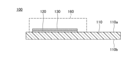
- FIG. 15 is a cross-sectional view (part 2) illustrating the strain gauge according to the first embodiment.
- FIG. 15 shows the cross-sectional shape of the strain gauge 100 when a functional layer 120 is provided as an underlayer for the resistor 130, wiring 140, and electrode 150.
- the planar shape of the functional layer 120 may be patterned to be substantially the same as the planar shapes of the resistor 130, the wiring 140, and the electrodes 150, for example. However, the planar shapes of the functional layer 120 and the resistor 130, the wiring 140, and the electrodes 150 do not have to be substantially the same.
- the functional layer 120 when the functional layer 120 is formed from an insulating material, the functional layer 120 may be patterned to be different from the planar shapes of the resistor 130, the wiring 140, and the electrodes 150.
- the functional layer 120 may be formed in a solid shape in the area where the resistor 130, the wiring 140, and the electrodes 150 are formed, for example.
- the functional layer 120 may be formed in a solid shape on the entire upper surface of the substrate 110.
- a cover layer 160 is formed on the upper surface 110a of the substrate 110 as necessary.
- the cover layer 160 covers the resistor 130 and wiring 140, but the electrodes 150 may be exposed from the cover layer 160.
- the cover layer 160 can be formed by laminating a semi-cured thermosetting insulating resin film on the upper surface 110a of the substrate 110 so as to cover the resistor 130 and wiring 140 and expose the electrodes 150, and then heating and curing the insulating resin film. Through the above steps, the strain gauge 100 is completed.
- FIG. 16 is a diagram (part 1) explaining the biasing member, and is a partial cross-sectional view showing the tubular portion 10, the pulse wave sensor 20, and the lid portion 30.
- the biasing member 60 is disposed between the first surface 23a of the opposing portion 23 and the second surface 30a of the lid portion 30 on the inside of the tubular portion 10, which is different from the structure shown in FIG. 8.
- the biasing member 60 can be arranged so as to be in contact with the first surface 23a of the facing portion 23 and the second surface 30a of the lid portion 30. By arranging the biasing member 60, the pulse wave sensor 20 can be biased in a direction away from the second surface 30a of the lid portion 30.
- FIG. 17 is a second diagram for explaining the biasing member, and is a perspective view showing only the biasing member.
- the biasing member 60 is, for example, a helical (spiral) leaf spring.
- the biasing member 60 can be positioned so that the pivot portion 23p is approximately at the center in a plan view.
- the biasing member 60 can be formed, for example, from metal, resin, rubber, etc.
- the biasing member 60 may be a conical spring or a cylindrical spring, but if it is a conical spring, the height when compressed can be made lower than if it were a cylindrical spring, making it possible to reduce the height of the tubular section 10. If the biasing member 60 is a conical spring, it is preferable to position the smaller diameter part of the conical spring facing the lid section 30 in order to stably position the biasing member 60.
- the shape and material of the biasing member 60 are not important as long as it can bias the pulse wave sensor 20 in a direction away from the second surface 30a of the lid portion 30.
- the biasing member 60 By arranging the biasing member 60 in this manner, even if vibrations or the like are applied to the pulse wave sensor 20 when it is not in contact with the subject's wrist, etc., the flange portion 23f can be maintained in contact with the step surface 10a, preventing rattle from occurring between the pulse wave sensor 20 and the cover portion 30. This can reduce the risk of abnormal noises occurring when carrying the pulse wave measuring device 1, for example.
- a pivot portion 23p is provided on the first surface 23a of the facing portion 23, and a recess 30x into which the pivot portion 23p can be inserted is opened on the second surface 30a of the lid portion 30.
- this is not limited to this, and a structure in which a pivot portion is provided on the second surface 30a of the lid portion 30, and a recess into which the pivot portion can be inserted is opened on the first surface 23a of the facing portion 23, may also be used.
- a pivot portion is provided on one of the first surface 23a of the facing portion 23 and the second surface 30a of the lid portion 30, and a recess into which the pivot portion can be inserted is opened on the other of the first surface 23a and the second surface 30a.
- the attachment portion 40 may be a watch strap type or the like, rather than a clip type as shown in FIG. 3 etc.
- the first curved member 41 and the second curved member 42 may be formed from leather or rubber etc., and the ends of the first curved member 41 and the second curved member 42 may be configured to be removably connected to each other using a hook-and-loop fastener or the like.
- the first curved member 41 and the second curved member 42 may be integrated into a single belt shape made of a stretchable material.
- the structure of the pulse wave sensor 20 is not limited to that shown in FIG. 10, etc., and may be any structure.
- a structure without slits around the beam portion may be used.
- the first surface side of the strain generating body may be covered with resin or the like.
- Pulse wave measuring device 10 Cylindrical portion, 10a Step surface, 10b Positioning portion, 10x Groove, 20 Pulse wave sensor, 21 Housing, 21x Groove, 22 Strain generating body, 22a Base portion, 22b Beam portion, 22c Loading portion, 22d Extension portion, 22m First main surface, 22n Second main surface, 23 Opposing portion, 23a First surface, 23f Flange portion, 23p Pivot portion, 23x Through hole, 23y Notch portion, 24 Screw, 25 Wire rod, 30 Lid portion, 30a Second surface, 30b Third surface, 30x Concave portion, 30y Convex portion, 30z Through hole, 32 Screw, 40 Mounting portion, 41 First curved member, 41x Groove, 42 Second curved member, 43 Pressing member, 44 Swing shaft, 45 First operation section, 46 Second operation section, 47 Part arrangement area, 48 Cover member, 49 Screw, 51 Wiring board, 52 Battery, 53 Wire rod, 60 Pressing member, 100 1 , 100 2 , 100 3
Landscapes
- Health & Medical Sciences (AREA)
- Life Sciences & Earth Sciences (AREA)
- Cardiology (AREA)
- Biomedical Technology (AREA)
- Medical Informatics (AREA)
- Biophysics (AREA)
- Pathology (AREA)
- Engineering & Computer Science (AREA)
- Veterinary Medicine (AREA)
- Heart & Thoracic Surgery (AREA)
- Physics & Mathematics (AREA)
- Molecular Biology (AREA)
- Surgery (AREA)
- Animal Behavior & Ethology (AREA)
- General Health & Medical Sciences (AREA)
- Public Health (AREA)
- Physiology (AREA)
- Vascular Medicine (AREA)
- Measuring Pulse, Heart Rate, Blood Pressure Or Blood Flow (AREA)
Abstract
Description
[脈波測定装置1]
図1は、第1実施形態に係る脈波測定装置を例示する斜視図(その1)であり、脈波測定装置を被験者の手首に装着した様子を模式的に示している。図2は、第1実施形態に係る脈波測定装置を例示する斜視図(その2)である。図3は、第1実施形態に係る脈波測定装置を例示する側面図である。
ここでは、脈波センサ20の一例として、複数のひずみゲージを有する脈波センサの例を示す。脈波センサ20の構成要素において、すでに説明した部分については、重複する説明は省略する。
図13は、第1実施形態に係るひずみゲージを例示する平面図である。図14は、第1実施形態に係るひずみゲージを例示する断面図(その1)であり、図13のB-B線に沿う断面を示している。
本実施形態に係るひずみゲージ100では、基材110上に、抵抗体130と、配線140と、電極150と、カバー層160とが形成される。なお、基材110とこれらの部材の層の間に別の層(後述する機能層等)が形成されてもよい。
第1実施形態の変形例1では、脈波センサと蓋部との間に付勢部材を配置する例を示す。なお、第1実施形態の変形例1では、既に説明した実施形態と同一の構成部についての説明は省略する場合がある。
Claims (12)
- 筒状部と、
筐体、前記筐体の一方側に設けられた起歪体、及び前記筐体の他方側に設けられた対向部を備え、前記起歪体が前記筒状部の軸方向の一端側から露出するように前記筒状部の内側に保持された脈波センサと、
前記筒状部の軸方向の他端側に固定された蓋部と、
前記筒状部の外側に連結され、被験者に装着可能な装着部と、を有し、
前記対向部の第1面と、前記蓋部の第2面とは、互いに対向し、
前記第1面及び前記第2面の一方にピボット部が設けられ、前記第1面及び前記第2面の他方に前記ピボット部を挿入可能な凹部が開口し、
前記ピボット部と前記凹部とが接触すると、前記脈波センサは、前記ピボット部と前記凹部との接触部分を支点として揺動可能となる、脈波測定装置。 - 前記装着部が前記被験者に装着されていないとき、前記ピボット部と前記凹部が接触しない第1状態となり、
前記装着部が前記被験者に装着されると、前記ピボット部と前記凹部が接触する第2状態に切り替わる、請求項1に記載の脈波測定装置。 - 前記第2状態では、前記ピボット部と前記凹部が線接触する、請求項2に記載の脈波測定装置。
- 前記ピボット部の前記凹部側はドーム状であり、
前記凹部の内側面は、前記筒状部の軸方向に対して傾斜する1つの曲面である、請求項1乃至3のいずれか一項に記載の脈波測定装置。 - 前記凹部は、円錐状または円錐台状である、請求項4に記載の脈波測定装置。
- 前記対向部は、前記筐体の外側面から前記筐体の径方向の外側に突出するフランジ部を有し、
前記筒状部の内側面は、軸側に突出する段差面を有し、
前記フランジ部は、前記段差面と前記第2面との間に配置され、
前記フランジ部は、前記脈波センサが前記筒状部から抜け落ちることを防止するストッパーとなる、請求項1乃至5のいずれか一項に記載の脈波測定装置。 - 前記蓋部は、前記第2面とは反対側の第3面に凸部を有し、
前記凹部は、前記筒状部の軸方向に視て、前記凸部と重なる位置に配置され、
前記凹部の一部は、前記凸部内に配置されている、請求項1乃至6のいずれか一項に記載の脈波測定装置。 - 前記第1面と前記第2面との間に、前記脈波センサを前記第2面から離れる方向に付勢する第1付勢部材が配置されている、請求項1乃至7のいずれか一項に記載の脈波測定装置。
- 前記起歪体は、複数のひずみゲージを有し、
前記脈波センサは、複数の前記ひずみゲージの抵抗体の抵抗値の変化に基づいて脈波を検出する、請求項1乃至8のいずれか一項に記載の脈波測定装置。 - 複数の前記ひずみゲージは、前記起歪体の圧縮ひずみを検出する一対のひずみゲージと、前記起歪体の引張ひずみを検出する他の一対のひずみゲージと、を含み、
一対の前記ひずみゲージ及び他の一対の前記ひずみゲージは、1つのブリッジ回路の各辺を構成するように接続され、
前記脈波を示す信号は、前記ブリッジ回路により生成される、請求項9に記載の脈波測定装置。 - 前記装着部は、前記被験者の手首に装着できるように反対方向に湾曲して互いに対向する第1湾曲部材及び第2湾曲部材を有し、
前記第1湾曲部材と前記第2湾曲部材は、第2付勢部材に付勢されると共に、閉状態と開状態とを遷移可能に搖動軸に支持され、
前記筒状部は、前記第1湾曲部材の長手方向の一端側に配置され、
前記搖動軸は、前記第1湾曲部材の長手方向の他端側に配置されている、請求項1乃至10のいずれか一項に記載の脈波測定装置。 - 前記第1湾曲部材は、長手方向の一端側と他端側との間に配置された部品配置領域を有し、
前記部品配置領域には、脈波の検出に寄与する部品が配置されている、請求項11に記載の脈波測定装置。
Priority Applications (3)
| Application Number | Priority Date | Filing Date | Title |
|---|---|---|---|
| CN202480034227.XA CN121174983A (zh) | 2023-06-06 | 2024-05-21 | 脉搏波测量装置 |
| KR1020257039414A KR20260003113A (ko) | 2023-06-06 | 2024-05-21 | 맥파 측정 장치 |
| EP24819149.6A EP4725405A1 (en) | 2023-06-06 | 2024-05-21 | Pulse wave measurement device |
Applications Claiming Priority (2)
| Application Number | Priority Date | Filing Date | Title |
|---|---|---|---|
| JP2023093415A JP2024175547A (ja) | 2023-06-06 | 2023-06-06 | 脈波測定装置 |
| JP2023-093415 | 2023-06-06 |
Publications (1)
| Publication Number | Publication Date |
|---|---|
| WO2024252916A1 true WO2024252916A1 (ja) | 2024-12-12 |
Family
ID=93795212
Family Applications (1)
| Application Number | Title | Priority Date | Filing Date |
|---|---|---|---|
| PCT/JP2024/018617 Ceased WO2024252916A1 (ja) | 2023-06-06 | 2024-05-21 | 脈波測定装置 |
Country Status (5)
| Country | Link |
|---|---|
| EP (1) | EP4725405A1 (ja) |
| JP (1) | JP2024175547A (ja) |
| KR (1) | KR20260003113A (ja) |
| CN (1) | CN121174983A (ja) |
| WO (1) | WO2024252916A1 (ja) |
Citations (5)
| Publication number | Priority date | Publication date | Assignee | Title |
|---|---|---|---|---|
| JPH01288228A (ja) * | 1988-05-16 | 1989-11-20 | Koorin Denshi Kk | 脈波検出装置 |
| JP5094131B2 (ja) | 2007-01-15 | 2012-12-12 | フクダ電子株式会社 | クリップ式電極 |
| JP2017121405A (ja) * | 2016-01-08 | 2017-07-13 | オムロンヘルスケア株式会社 | 圧脈波測定装置及び生体情報測定装置 |
| JP2017189511A (ja) * | 2016-04-15 | 2017-10-19 | オムロンヘルスケア株式会社 | 脈波検出装置、生体情報測定装置、脈波検出装置の制御方法、及び、脈波検出装置の制御プログラム |
| JP2023093415A (ja) | 2021-12-22 | 2023-07-04 | 北京交通大学 | ランタイム検証に基づく列車スケジューリング操作の危険予測方法及びシステム |
-
2023
- 2023-06-06 JP JP2023093415A patent/JP2024175547A/ja active Pending
-
2024
- 2024-05-21 CN CN202480034227.XA patent/CN121174983A/zh active Pending
- 2024-05-21 EP EP24819149.6A patent/EP4725405A1/en active Pending
- 2024-05-21 WO PCT/JP2024/018617 patent/WO2024252916A1/ja not_active Ceased
- 2024-05-21 KR KR1020257039414A patent/KR20260003113A/ko active Pending
Patent Citations (5)
| Publication number | Priority date | Publication date | Assignee | Title |
|---|---|---|---|---|
| JPH01288228A (ja) * | 1988-05-16 | 1989-11-20 | Koorin Denshi Kk | 脈波検出装置 |
| JP5094131B2 (ja) | 2007-01-15 | 2012-12-12 | フクダ電子株式会社 | クリップ式電極 |
| JP2017121405A (ja) * | 2016-01-08 | 2017-07-13 | オムロンヘルスケア株式会社 | 圧脈波測定装置及び生体情報測定装置 |
| JP2017189511A (ja) * | 2016-04-15 | 2017-10-19 | オムロンヘルスケア株式会社 | 脈波検出装置、生体情報測定装置、脈波検出装置の制御方法、及び、脈波検出装置の制御プログラム |
| JP2023093415A (ja) | 2021-12-22 | 2023-07-04 | 北京交通大学 | ランタイム検証に基づく列車スケジューリング操作の危険予測方法及びシステム |
Also Published As
| Publication number | Publication date |
|---|---|
| CN121174983A (zh) | 2025-12-19 |
| JP2024175547A (ja) | 2024-12-18 |
| KR20260003113A (ko) | 2026-01-06 |
| EP4725405A1 (en) | 2026-04-15 |
Similar Documents
| Publication | Publication Date | Title |
|---|---|---|
| US20250009242A1 (en) | Pulse wave measuring device | |
| JP7789492B2 (ja) | 脈波センサ | |
| JP2023138686A (ja) | センサモジュール | |
| JP2024175547A (ja) | 脈波測定装置 | |
| JP7623065B2 (ja) | 脈波測定装置 | |
| WO2025028318A1 (ja) | 脈波測定装置 | |
| WO2025041723A1 (ja) | 脈波測定装置 | |
| JP2024179645A (ja) | 脈波測定装置 | |
| JP2022182909A (ja) | バイタルセンサ | |
| JP2023039125A (ja) | 脈波センサ | |
| EP4691351A1 (en) | Pulse wave sensor | |
| JP2024117474A (ja) | 押圧力センサ | |
| WO2024204574A1 (ja) | 脈波センサ | |
| JP7845619B2 (ja) | 脈波測定装置 | |
| JP7838220B2 (ja) | 脈波測定装置 | |
| JP2024143982A (ja) | 脈波センサ | |
| JP2024143983A (ja) | 脈波センサ | |
| US20250155306A1 (en) | Pulse wave sensor | |
| WO2024190692A1 (ja) | 脈波センサ | |
| JP2024098234A (ja) | 脈波センサ | |
| US20250228464A1 (en) | Pulse wave sensor | |
| JP2023021714A (ja) | 脈波測定装置 | |
| JP2025021155A (ja) | 脈波計測装置 | |
| WO2022249717A1 (ja) | バイタルセンサ |
Legal Events
| Date | Code | Title | Description |
|---|---|---|---|
| 121 | Ep: the epo has been informed by wipo that ep was designated in this application |
Ref document number: 24819149 Country of ref document: EP Kind code of ref document: A1 |
|
| ENP | Entry into the national phase |
Ref document number: 1020257039414 Country of ref document: KR Free format text: ST27 STATUS EVENT CODE: A-0-1-A10-A15-NAP-PA0105 (AS PROVIDED BY THE NATIONAL OFFICE) |
|
| WWE | Wipo information: entry into national phase |
Ref document number: 2024819149 Country of ref document: EP |
|
| NENP | Non-entry into the national phase |
Ref country code: DE |
|
| ENP | Entry into the national phase |
Ref document number: 2024819149 Country of ref document: EP Effective date: 20260107 |
|
| ENP | Entry into the national phase |
Ref document number: 2024819149 Country of ref document: EP Effective date: 20260107 |
|
| ENP | Entry into the national phase |
Ref document number: 2024819149 Country of ref document: EP Effective date: 20260107 |
|
| ENP | Entry into the national phase |
Ref document number: 2024819149 Country of ref document: EP Effective date: 20260107 |
|
| ENP | Entry into the national phase |
Ref document number: 2024819149 Country of ref document: EP Effective date: 20260107 |
|
| WWP | Wipo information: published in national office |
Ref document number: 2024819149 Country of ref document: EP |