WO2024252845A1 - 半導体装置、および半導体装置の製造方法 - Google Patents
半導体装置、および半導体装置の製造方法 Download PDFInfo
- Publication number
- WO2024252845A1 WO2024252845A1 PCT/JP2024/017398 JP2024017398W WO2024252845A1 WO 2024252845 A1 WO2024252845 A1 WO 2024252845A1 JP 2024017398 W JP2024017398 W JP 2024017398W WO 2024252845 A1 WO2024252845 A1 WO 2024252845A1
- Authority
- WO
- WIPO (PCT)
- Prior art keywords
- electrode
- thickness direction
- back surface
- conductive member
- semiconductor device
- Prior art date
- Legal status (The legal status is an assumption and is not a legal conclusion. Google has not performed a legal analysis and makes no representation as to the accuracy of the status listed.)
- Ceased
Links
Images





Classifications
-
- H—ELECTRICITY
- H10—SEMICONDUCTOR DEVICES; ELECTRIC SOLID-STATE DEVICES NOT OTHERWISE PROVIDED FOR
- H10W—GENERIC PACKAGES, INTERCONNECTIONS, CONNECTORS OR OTHER CONSTRUCTIONAL DETAILS OF DEVICES COVERED BY CLASS H10
- H10W70/00—Package substrates; Interposers; Redistribution layers [RDL]
- H10W70/40—Leadframes
- H10W70/411—Chip-supporting parts, e.g. die pads
- H10W70/417—Bonding materials between chips and die pads
-
- H—ELECTRICITY
- H10—SEMICONDUCTOR DEVICES; ELECTRIC SOLID-STATE DEVICES NOT OTHERWISE PROVIDED FOR
- H10W—GENERIC PACKAGES, INTERCONNECTIONS, CONNECTORS OR OTHER CONSTRUCTIONAL DETAILS OF DEVICES COVERED BY CLASS H10
- H10W72/00—Interconnections or connectors in packages
-
- H—ELECTRICITY
- H10—SEMICONDUCTOR DEVICES; ELECTRIC SOLID-STATE DEVICES NOT OTHERWISE PROVIDED FOR
- H10W—GENERIC PACKAGES, INTERCONNECTIONS, CONNECTORS OR OTHER CONSTRUCTIONAL DETAILS OF DEVICES COVERED BY CLASS H10
- H10W72/00—Interconnections or connectors in packages
- H10W72/071—Connecting or disconnecting
-
- H—ELECTRICITY
- H10—SEMICONDUCTOR DEVICES; ELECTRIC SOLID-STATE DEVICES NOT OTHERWISE PROVIDED FOR
- H10W—GENERIC PACKAGES, INTERCONNECTIONS, CONNECTORS OR OTHER CONSTRUCTIONAL DETAILS OF DEVICES COVERED BY CLASS H10
- H10W72/00—Interconnections or connectors in packages
- H10W72/071—Connecting or disconnecting
- H10W72/076—Connecting or disconnecting of strap connectors
- H10W72/07631—Techniques
- H10W72/07636—Soldering or alloying
-
- H—ELECTRICITY
- H10—SEMICONDUCTOR DEVICES; ELECTRIC SOLID-STATE DEVICES NOT OTHERWISE PROVIDED FOR
- H10W—GENERIC PACKAGES, INTERCONNECTIONS, CONNECTORS OR OTHER CONSTRUCTIONAL DETAILS OF DEVICES COVERED BY CLASS H10
- H10W72/00—Interconnections or connectors in packages
- H10W72/60—Strap connectors, e.g. thick copper clips for grounding of power devices
- H10W72/621—Structures or relative sizes of strap connectors
- H10W72/627—Multiple strap connectors having different structures or shapes
-
- H—ELECTRICITY
- H10—SEMICONDUCTOR DEVICES; ELECTRIC SOLID-STATE DEVICES NOT OTHERWISE PROVIDED FOR
- H10W—GENERIC PACKAGES, INTERCONNECTIONS, CONNECTORS OR OTHER CONSTRUCTIONAL DETAILS OF DEVICES COVERED BY CLASS H10
- H10W72/00—Interconnections or connectors in packages
- H10W72/60—Strap connectors, e.g. thick copper clips for grounding of power devices
- H10W72/631—Shapes of strap connectors
- H10W72/634—Cross-sectional shape
-
- H—ELECTRICITY
- H10—SEMICONDUCTOR DEVICES; ELECTRIC SOLID-STATE DEVICES NOT OTHERWISE PROVIDED FOR
- H10W—GENERIC PACKAGES, INTERCONNECTIONS, CONNECTORS OR OTHER CONSTRUCTIONAL DETAILS OF DEVICES COVERED BY CLASS H10
- H10W72/00—Interconnections or connectors in packages
- H10W72/60—Strap connectors, e.g. thick copper clips for grounding of power devices
- H10W72/631—Shapes of strap connectors
- H10W72/637—Multiple strap connectors having different shapes
-
- H—ELECTRICITY
- H10—SEMICONDUCTOR DEVICES; ELECTRIC SOLID-STATE DEVICES NOT OTHERWISE PROVIDED FOR
- H10W—GENERIC PACKAGES, INTERCONNECTIONS, CONNECTORS OR OTHER CONSTRUCTIONAL DETAILS OF DEVICES COVERED BY CLASS H10
- H10W90/00—Package configurations
- H10W90/701—Package configurations characterised by the relative positions of pads or connectors relative to package parts
- H10W90/731—Package configurations characterised by the relative positions of pads or connectors relative to package parts of die-attach connectors
- H10W90/736—Package configurations characterised by the relative positions of pads or connectors relative to package parts of die-attach connectors between a chip and a stacked lead frame, conducting package substrate or heat sink
-
- H—ELECTRICITY
- H10—SEMICONDUCTOR DEVICES; ELECTRIC SOLID-STATE DEVICES NOT OTHERWISE PROVIDED FOR
- H10W—GENERIC PACKAGES, INTERCONNECTIONS, CONNECTORS OR OTHER CONSTRUCTIONAL DETAILS OF DEVICES COVERED BY CLASS H10
- H10W72/00—Interconnections or connectors in packages
- H10W72/851—Dispositions of multiple connectors or interconnections
- H10W72/874—On different surfaces
- H10W72/886—Die-attach connectors and strap connectors
Definitions
- This disclosure relates to a semiconductor device and a method for manufacturing a semiconductor device.
- Patent Document 1 discloses an example of a conventional semiconductor device.
- the semiconductor device disclosed in this document includes multiple leads and a semiconductor element.
- a source electrode (first electrode) and a gate electrode (second electrode) are formed on the main surface of the semiconductor element. Pad portions of the leads are bonded to the source electrode and the gate electrode via bonding material, respectively.
- the area of the gate electrode is smaller than the area of the source electrode, and the bonding area of the lead bonded to the gate electrode is smaller than the bonding area of the lead bonded to the source electrode.
- the distance between each electrode and the bonding surface of the lead bonded to it may have a dimensional error. If the distance between the gate electrode, which has a relatively small area, and the bonding surface of the lead bonded to the gate electrode becomes larger than the set dimension, there is a concern that defects such as poor bonding may occur at the bonding portion between the gate electrode and the lead.
- An object of the present disclosure is to provide a semiconductor device that is an improvement over conventional semiconductor devices.
- an object of the present disclosure is to provide a semiconductor device that is suitable for improving the bonding reliability between an electrode on a semiconductor element and a conductive member bonded to the electrode.
- the semiconductor device provided by the first aspect of the present disclosure includes a semiconductor element having a first electrode and a second electrode arranged on one side in the thickness direction, a first conductive member located on one side in the thickness direction with respect to the first electrode and having a first back surface facing the other side in the thickness direction, a second conductive member located on one side in the thickness direction with respect to the second electrode and having a second back surface facing the other side in the thickness direction, a first conductive bonding material interposed between the first electrode and the first back surface and bonded to the first electrode and the first conductive member, and a second conductive bonding material interposed between the second electrode and the second back surface and bonded to the second electrode and the second conductive member.
- the area of the second back surface is smaller than the area of the first back surface.
- a second distance between the second electrode and the second back surface in the thickness direction is smaller than a first distance between the first electrode and the first back surface in the thickness direction.
- a method for manufacturing a semiconductor device includes the steps of: arranging a first bonding layer and a second bonding layer on a first electrode and a second electrode of a semiconductor element having a first electrode and a second electrode arranged on one side in a thickness direction; arranging a metal clip member having a first conductive portion and a second conductive portion connected to each other on one side in the thickness direction of the semiconductor element; and heating, melting, and solidifying the first bonding layer and the second bonding layer while pressing the metal clip member against the other side in the thickness direction against the semiconductor element.
- the first conductive portion has a first back surface that overlaps the first bonding layer when viewed in the thickness direction and faces the other side in the thickness direction.
- the second conductive portion has a second back surface that overlaps the second bonding layer when viewed in the thickness direction and faces the other side in the thickness direction.
- the second back surface is located on the other side in the thickness direction than the first back surface.
- FIG. 1 is a perspective view showing a semiconductor device according to a first embodiment of the present disclosure.
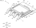
- FIG. 2 is a perspective view of a main part of the semiconductor device according to the first embodiment of the present disclosure.
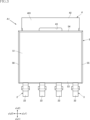
- FIG. 3 is a plan view showing the semiconductor device according to the first embodiment of the present disclosure.
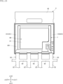
- FIG. 4 is a plan view showing a main part of the semiconductor device according to the first embodiment of the present disclosure.
- FIG. 5 is a bottom view showing the semiconductor device according to the first embodiment of the present disclosure.
- FIG. 6 is a bottom view of a main portion showing the semiconductor device according to the first embodiment of the present disclosure.
- FIG. 7 is a side view showing the semiconductor device according to the first embodiment of the present disclosure.
- FIG. 8 is a cross-sectional view taken along line VIII-VIII in FIG.
- FIG. 9 is a cross-sectional view taken along line IX-IX in FIG.
- FIG. 10 is a cross-sectional view taken along line XX in FIG.
- FIG. 11 is a partially enlarged view of FIG.
- FIG. 12 is a partially enlarged view of FIG.
- FIG. 13 is a plan view showing a process in the manufacture of the semiconductor device according to the first embodiment of the present disclosure.
- FIG. 14 is a plan view showing a step subsequent to that shown in FIG.
- FIG. 15 is a partially enlarged side view of the step shown in FIG.
- FIG. 16 is a partially enlarged side view showing a step subsequent to that shown in FIG.
- FIG. 17 is a plan view of a main portion showing a semiconductor device according to a second embodiment of the present disclosure.
- FIG. 18 is a cross-sectional view taken along line XVIII-XVIII in FIG.
- FIG. 19 is a partially enlarged view of FIG.
- FIG. 20 is a plan view of a main portion showing a semiconductor device according to a third embodiment of the present disclosure.
- an object A is formed on an object B" and “an object A is formed on an object B” include “an object A is formed directly on an object B” and “an object A is formed on an object B with another object interposed between the object A and the object B” unless otherwise specified.
- an object A is disposed on an object B” and “an object A is disposed on an object B” include “an object A is disposed directly on an object B” and “an object A is disposed on an object B with another object interposed between the object A and the object B" unless otherwise specified.
- an object A is located on an object B includes “an object A is located on an object B in contact with an object B” and “an object A is located on an object B with another object interposed between the object A and the object B” unless otherwise specified.
- an object A overlaps an object B when viewed in a certain direction includes “an object A overlaps the entire object B” and “an object A overlaps a part of an object B.”
- a surface A faces in direction B is not limited to the case where the angle of surface A with respect to direction B is 90 degrees, but also includes the case where surface A is tilted with respect to direction B.
- First embodiment: 1 to 12 show a semiconductor device according to a first embodiment of the present disclosure.
- the semiconductor device A1 of this embodiment includes a semiconductor element 1, a first conductive member 2, a second conductive member 3, a third conductive member 4, and a sealing resin 5.
- the semiconductor device A1 further includes a conductive bonding material 19, a first conductive bonding material 29, and a second conductive bonding material 39.
- the application of the semiconductor device A1 is not limited in any way, and it is used in electronic devices including a power conversion circuit, such as a DC-DC converter.
- FIG. 1 is a perspective view of the semiconductor device A1.
- FIG. 2 is a perspective view of the main part of the semiconductor device A1, omitting the sealing resin 5.
- FIG. 3 is a plan view of the semiconductor device A1.
- FIG. 4 is a plan view of the main part of the semiconductor device A1, seen through the sealing resin 5.
- FIG. 5 is a bottom view of the semiconductor device A1.
- FIG. 6 is a bottom view of the main part of the semiconductor device A1, seen through the sealing resin 5.
- FIG. 7 is a side view of the semiconductor device A1.
- FIG. 8 is a cross-sectional view taken along line VIII-VIII in FIG. 4.
- FIG. 9 is a cross-sectional view taken along line IX-IX in FIG. 4.
- FIG. 10 is a cross-sectional view taken along line X-X in FIG. 4.
- FIG. 11 is a partial enlarged view of FIG. 8.
- FIG. 12 is a partial enlarged view of FIG. 9.
- FIG. 4 is a partial enlarged view. Note that in FIG. 4 and FIG. 6, the sealing resin 5 seen through is shown by an imaginary line (two-dot chain line).
- an example of the thickness direction is the "thickness direction z".
- the direction perpendicular to the thickness direction z (the up-down direction in Figures 3 and 4) is an example of the first direction and is called the "first direction x".
- the direction perpendicular to the thickness direction z and the first direction x (the left-right direction in Figures 3 and 4) is an example of the second direction and is called the "second direction y”.
- the lower side in the figure is an example of "one side of the first direction” and is called the "x1 side of the first direction x”
- the upper side in the figure is an example of "the other side of the first direction” and is called the "x2 side of the first direction x".
- the semiconductor element 1 is an element that exerts the electrical function of the semiconductor device A1.
- the semiconductor element 1 is a three-terminal element having three electrodes, for example a MOSFET (Metal-Oxide-Semiconductor Field-Effect Transistor).
- the semiconductor element 1 may be a switching element such as an IGBT (Insulated Gate Bipolar Transistor) or a diode.
- the semiconductor element 1 is an n-channel type MOSFET with a vertical structure.
- the semiconductor element 1 is rectangular when viewed in the thickness direction z.
- the semiconductor element 1 has a first element surface 101, a second element surface 102, a first electrode 11, a second electrode 12, and a third electrode 13.
- the first element surface 101 and the second element surface 102 are spaced apart in the thickness direction z and face opposite each other.
- the first element surface 101 faces the z1 side in the thickness direction z.
- the second element surface 102 faces the z2 side in the thickness direction z.
- the first electrode 11 is disposed on the first surface 101 of the element. A current corresponding to the power converted by the semiconductor element 1 flows through the first electrode 11. In other words, the first electrode 11 corresponds to the source electrode of the semiconductor element 1.
- the second electrode 12 is disposed on the first surface 101 of the element.
- a gate voltage for driving the semiconductor element 1 is applied to the second electrode 12.
- the second electrode 12 corresponds to the gate electrode of the semiconductor element 1.
- the area of the second electrode 12 is smaller than the area of the first electrode 11.
- the third electrode 13 is disposed on the first surface 101 of the element. A current corresponding to the power before being converted by the semiconductor element 1 flows through the third electrode 13. In other words, the third electrode 13 corresponds to the drain electrode of the semiconductor element 1.
- the first conductive member 2 includes a portion that is disposed on the z1 side of the semiconductor element 1 in the thickness direction z.
- the first conductive member 2 includes a conductive material such as metal, and is made of, for example, a metal plate material.
- the constituent material of the first conductive member 2 includes, for example, Cu (copper).
- the first conductive member 2 is a metal plate material that is appropriately bent. As shown in Figures 1 to 6 and 8 to 10, the first conductive member 2 has a pad portion 21 and multiple terminal portions 22.
- the pad portion 21 is a portion that is conductively joined to the first electrode 11 of the semiconductor element 1. There are no limitations on the shape or size of the pad portion 21, and in the illustrated example, the pad portion 21 is shaped to overlap most of the first electrode 11 when viewed in the thickness direction z, and also to expose the second electrode 12.
- the pad portion 21 has a first main surface 211 and a first back surface 212.
- the first main surface 211 is a surface facing the z1 side in the thickness direction z.
- the first back surface 212 is a surface facing the z2 side in the thickness direction z.
- the first back surface 212 of the pad portion 21 is bonded to the first electrode 11 of the semiconductor element 1 via the first conductive bonding material 29.
- the pad portion 21 and the first electrode 11 are conductively bonded to each other via the first conductive bonding material 29.
- the material of the first conductive bonding material 29 is not particularly limited, and may be, for example, solder (a metal containing tin and silver).
- the first conductive bonding material 29 may also be made of a metal paste containing a metal such as silver (Ag).
- the distance between the first electrode 11 and the first back surface 212 in the thickness direction z (first distance d1) is, for example, 5 ⁇ m or more and 30 ⁇ m or less.
- a plating layer made of, for example, silver (Ag) may be formed on the area of the pad portion 21 that is bonded to the semiconductor element 1 (first electrode 11).
- the multiple terminals 22 are connected to the pad 21 on the x1 side in the first direction x.
- the terminals 22 each extend in the first direction x when viewed in the thickness direction z, and are arranged at intervals in the second direction y.
- the number of the multiple terminals 22 is not limited, and may be three as in the illustrated example, or may be two, four or more. Also, a configuration may be provided with only one terminal 22.
- the terminal 22 has a portion connected to the pad 21 and covered with the sealing resin 5, a portion protruding from the sealing resin 5 to the x1 side in the first direction x, a portion folded back to the z2 side in the thickness direction z, and a portion located on the z2 side in the thickness direction z.
- the multiple terminals 22 are used as terminals when mounting the semiconductor device A1.
- the multiple terminals 22 are electrically connected to the first electrode 11 of the semiconductor element 1.
- the multiple terminals 22 are source terminals of the semiconductor device A1.
- a plating layer made of an alloy mainly composed of tin (Sn), for example, may be formed on the portion of the first conductive member 2 (multiple terminal portions 22) exposed from the sealing resin 5.
- the second conductive member 3 includes a portion that is disposed on the z1 side of the semiconductor element 1 in the thickness direction z.
- the second conductive member 3 includes a conductive material such as metal, and is made of, for example, a metal plate material.
- the material that makes up the second conductive member 3 includes, for example, Cu (copper).
- the second conductive member 3 is a metal plate material that is appropriately bent. As shown in Figures 1 to 7, 9, and 12, the second conductive member 3 has a first pad portion 31, a terminal portion 32, a first bent portion 33, and a second bent portion 34.
- the first pad portion 31 is a portion that is conductively joined to the second electrode 12 of the semiconductor element 1. There are no limitations on the shape or size of the first pad portion 31, and in the illustrated example, it is shaped to overlap a portion of the second electrode 12 when viewed in the thickness direction z, and also to expose the second electrode 12.
- the first pad portion 31 has a second main surface 311 and a second back surface 312.
- the second main surface 311 is a surface facing the z1 side in the thickness direction z.
- the second back surface 312 is a surface facing the z2 side in the thickness direction z.
- the area of the second back surface 312 is smaller than the area of the first back surface 212 of the pad portion 21 in the first conductive member 2.
- the first bent portion 33 is connected to the x1 side of the first direction x with respect to the first pad portion 31.
- the first bent portion 33 is inclined so as to be located on the z1 side of the thickness direction z as it approaches the x1 side of the first direction x.
- the second bent portion 34 is connected to the x2 side of the first direction x with respect to the first pad portion 31.
- the second bent portion 34 is inclined so as to be located on the z1 side of the thickness direction z as it approaches the x2 side of the first direction x.
- the inclination angle ⁇ 1 of the first bent portion 33 with respect to the first direction x and the inclination angle ⁇ 2 of the second bent portion 34 with respect to the first direction x are the same.
- the inclination angle ⁇ 1 and the inclination angle ⁇ 2 are the same” means that the inclination angle ⁇ 1 and the inclination angle ⁇ 2 are the same in design, and includes cases where the inclination angle ⁇ 1 and the inclination angle ⁇ 2 are different due to manufacturing errors, etc.
- the inclination angles ⁇ 1 and ⁇ 2 are not particularly limited, but in the illustrated example, the inclination angles ⁇ 1 and ⁇ 2 are approximately 45°.
- the first pad portion 31, the first bent portion 33, and the second bent portion 34 are bonded to the second electrode 12 of the semiconductor element 1 via the second conductive bonding material 39.
- the first pad portion 31, the first bent portion 33, and the second bent portion 34 are conductively bonded to the second electrode 12 via the second conductive bonding material 39.
- the second conductive bonding material 39 includes a thin portion 391, a first portion 392, and a second portion 393.
- the thin portion 391 is interposed between the second electrode 12 and the second back surface 312 in the thickness direction z, and is a portion that contacts the second electrode 12 and the second back surface 312.
- the first portion 392 is located on the x1 side of the thin portion 391 in the first direction x, and is a portion that contacts the second electrode 12 and the first bent portion 33.
- the second portion 393 is located on the x2 side of the thin portion 391 in the first direction x, and is in contact with the second electrode 12 and the second bent portion 34.
- the distance (second distance d2) between the second electrode 12 and the second back surface 312 in the thickness direction z is smaller than the distance (first distance d1) between the first electrode 11 and the first back surface 212 in the thickness direction z.
- the second distance d2 between the second electrode 12 and the second back surface 312 in the thickness direction z is, for example, 1 ⁇ m or more and 20 ⁇ m or less.
- the second electrode 12 and the second back surface 312 may be in partial contact.
- the ratio of the first distance d1 between the first electrode 11 and the first back surface 212 in the thickness direction z to the dimension t1 in the thickness direction z from the second back surface 312 to the second main surface 311 is, for example, 0.5% or more and 10% or less.
- the dimension t1 is, for example, about 0.1 mm or more and 1 mm or less.
- the constituent material of the second conductive bonding material 39 is not particularly limited, and may be, for example, solder (a metal containing tin and silver).
- the second conductive bonding material 39 may also be made of a metal paste containing a metal such as silver (Ag). Note that a plating layer made of, for example, silver (Ag) may be formed on the areas of the first pad portion 31, the first bent portion 33, and the second bent portion 34 that are bonded to the semiconductor element 1 (second electrode 12).
- the terminal portion 32 is connected to the first bent portion 33 on the x1 side in the first direction x.
- the terminal portion 32 extends in the first direction x when viewed in the thickness direction z.
- the terminal portion 32 has a portion connected to the first bent portion 33 and covered with the sealing resin 5, a portion protruding from the sealing resin 5 to the x1 side in the first direction x, a portion folded back to the z2 side in the thickness direction z, and a portion located on the z2 side in the thickness direction z.
- the terminal portion 32 When viewed in the second direction y, the terminal portion 32 has a shape and size that roughly overlaps with the terminal portion 22.
- the terminal portion 32 is used as a terminal when mounting the semiconductor device A1.
- the terminal portion 32 is electrically connected to the second electrode 12 of the semiconductor element 1.
- the terminal portion 32 is a gate terminal of the semiconductor device A1.
- a plating layer made of an alloy mainly composed of tin (Sn), for example, may be formed on the portion of the second conductive member 3 (terminal portion 32) exposed from the sealing resin 5.
- the third conductive member 4 is disposed on the z2 side of the semiconductor element 1 in the thickness direction z.
- the third conductive member 4 includes a conductive material such as a metal, for example, copper (Cu).
- the third conductive member 4 has a main surface 401 and a back surface 402.
- the main surface 401 faces the z1 side in the thickness direction z.
- the back surface 402 faces the z2 side in the thickness direction z.
- the semiconductor element 1 is mounted on the main surface 401.
- the back surface 402 is exposed from the sealing resin 5.
- the third conductive member 4 has an island portion 41, a terminal portion 42, and a through hole 43.
- the island portion 41 is a portion on which the entire or part of the semiconductor element 1 is mounted.
- the island portion 41 includes a part of the main surface 401 and a part of the back surface 402. There are no limitations on the shape or size of the island portion 41, and in the illustrated example, it is substantially rectangular when viewed in the thickness direction z.
- the island portion 41 has a first edge portion 411, a second edge portion 412, a third edge portion 413, and a groove 414.
- the first edge portion 411 is located on the y1 side of the second direction y and extends in the first direction x.
- the second edge portion 412 is located on the y2 side of the second direction y and extends in the first direction x.
- the third edge portion 413 is located on the x1 side of the first direction x and extends in the second direction y.
- the groove 414 is recessed from the main surface 401 to the z2 side of the thickness direction z, and has a generally V-shaped cross section.
- the groove 414 surrounds the semiconductor element 1 when viewed in the thickness direction z.
- Each of the first edge portion 411, the second edge portion 412, the third edge portion 413, and the groove 414 is covered with the sealing resin 5.
- the island portion 41 may be configured without the recessed groove 414.
- the first edge portion 411 has a first step portion 411a, as shown in Figures 4 and 6.
- the first step portion 411a is formed on the x2 side of the first direction x relative to the semiconductor element 1 in the first direction x.
- the first step portion 411a is shaped so that the x2 side of the first direction x is recessed toward the y2 side of the second direction y relative to the x1 side of the first direction x.
- the first step portion 411a is inclined with respect to the first direction x and the second direction y so that it is positioned on the y2 side of the second direction y as it approaches the x2 side of the first direction x in the first direction x.
- the second edge portion 412 has a second step portion 412a.
- the second step portion 412a is formed on the x2 side of the first direction x relative to the semiconductor element 1 in the first direction x.
- the second step portion 412a is shaped so that the x2 side of the first direction x is recessed toward the y1 side of the second direction y relative to the x1 side of the first direction x.
- the second step portion 412a is inclined with respect to the first direction x and the second direction y so that it is positioned on the y1 side of the second direction y as it approaches the x2 side of the first direction x in the first direction x.
- the island portion 41 includes a main portion 41A, a first thin portion 41B, and a second thin portion 41C, as shown in Figures 4, 6, and 10.
- the main portion 41A has a portion of the main surface 401 and a portion of the back surface 402.
- the first thin portion 41B is a portion that is connected to the y1 side of the main portion 41A in the second direction y.
- the first thin portion 41B has a part of the main surface 401 and a first intermediate surface 403.
- the first thin portion 41B is a portion that does not have a back surface 402.
- the first intermediate surface 403 faces the z2 side in the thickness direction z.
- the first intermediate surface 403 is located between the main surface 401 and the back surface 402 in the thickness direction z.
- the first thin portion 41B has a shape that is recessed on the z2 side in the thickness direction z with respect to the main portion 41A.
- the first thin portion 41B includes the entire first edge portion 411.
- the first step portion 411a is formed in the first thin portion 41B.
- the second thin portion 41C is a portion that is connected to the y2 side of the main portion 41A in the second direction y.
- the second thin portion 41C has a part of the main surface 401 and a second intermediate surface 404.
- the second thin portion 41C is a portion that does not have a back surface 402.
- the second intermediate surface 404 faces the z2 side of the thickness direction z.
- the second intermediate surface 404 is located between the main surface 401 and the back surface 402 in the thickness direction z.
- the second thin portion 41C has a shape that is recessed on the z2 side of the thickness direction z with respect to the main portion 41A.
- the second thin portion 41C includes the entire second edge portion 412.
- the second step portion 412a is formed in the second thin portion 41C.
- the semiconductor element 1 overlaps the main portion 41A and the first thin portion 41B when viewed in the thickness direction z. Also, the semiconductor element 1 overlaps the main portion 41A and the second thin portion 41C when viewed in the thickness direction z.
- the semiconductor element 1 is bonded to the main surface 401 of the island portion 41 via a conductive bonding material 19.
- the second element surface 102 of the semiconductor element 1 faces the main surface 401.
- the third electrode 13 on the second element surface 102 and the main surface 401 are conductively bonded via the conductive bonding material 19.
- the material of the conductive bonding material 19 is not particularly limited, and may be, for example, solder (a metal containing tin and silver).
- the conductive bonding material 19 may also be made of a metal paste containing a metal such as silver (Ag).
- a plating layer made of, for example, silver (Ag) may be formed on the area of the main surface 401 of the island portion 41 where the semiconductor element 1 is bonded.
- the terminal portion 42 is a portion that is connected to the x2 side of the island portion 41 in the first direction x.
- the terminal portion 42 includes a portion of the main surface 401 and a portion of the back surface 402.
- the terminal portion 42 may be used as a terminal when mounting the semiconductor device A1.
- the terminal portion 42 is electrically connected to the third electrode 13 of the semiconductor element 1.
- the terminal portion 42 is a drain terminal of the semiconductor device A1.
- the through hole 43 penetrates the third conductive member 4 in the thickness direction z.
- the through hole 43 is filled with a portion of the sealing resin 5.
- the size of the cross section of the through hole 43 perpendicular to the thickness direction z is larger on the z2 side of the thickness direction z than on the z1 side of the thickness direction z. This has the effect of, for example, preventing the third conductive member 4 from falling off the sealing resin 5.
- a plating layer made of an alloy mainly composed of tin (Sn), for example, may be formed on the portion of the third conductive member 4 exposed from the sealing resin 5.
- the sealing resin 5 covers the semiconductor element 1 and a portion of each of the first conductive member 2, the second conductive member 3, and the third conductive member 4.
- the sealing resin 5 has electrical insulation properties.
- the sealing resin 5 includes, for example, a black epoxy resin containing a filler.
- the shape of the sealing resin 5 is not limited in any way.
- the sealing resin 5 of this embodiment has a first resin surface 51, a second resin surface 52, a third resin surface 53, a fourth resin surface 54, a fifth resin surface 55, and a sixth resin surface 56, as shown in Figures 1 and 3 to 10.
- the first resin surface 51 faces the z1 side in the thickness direction z.
- the second resin surface 52 faces the z2 side in the thickness direction z.
- the back surface 402 of the third conductive member 4 is exposed from the second resin surface 52.
- the first resin surface 51 and the second resin surface 52 are flat surfaces, but are not limited to this and may be curved or bent surfaces, for example.
- the second resin surface 52 and the back surface 402 are flush with each other.
- the third resin surface 53 is a surface facing the x1 side in the first direction x.
- the fourth resin surface 54 is a surface facing the x2 side in the first direction x.
- the third resin surface 53 and the fourth resin surface 54 are slightly curved surfaces, but are not limited to this and may be curved surfaces or flat surfaces, for example.
- a plurality of terminal portions 22 and terminal portion 32 protrude from the third resin surface 53, and terminal portion 42 protrudes from the fourth resin surface 54.
- the fifth resin surface 55 is a surface facing the y1 side in the second direction y.
- the sixth resin surface 56 is a surface facing the y2 side in the second direction y.
- the fifth resin surface 55 and the sixth resin surface 56 are slightly curved surfaces, but are not limited to this and may be, for example, curved surfaces or flat surfaces.
- Figures 13 and 14 are plan views showing a step in the manufacture of the semiconductor device A1.
- Figure 15 is a partially enlarged side view of the step shown in Figure 14.
- Figure 16 is a partially enlarged side view showing the step following Figure 15.
- FIGS. 14 and 15 show a state in which the first bonding layer 929 and the second bonding layer 939 are disposed on the semiconductor element 1 mounted on the third conductive member 4.
- the first bonding layer 929 and the first bonding layer 929 will later become the first conductive bonding material 29 and the second conductive bonding material 39, and are, for example, solder paste applied by a dispenser.
- a metal clip member 90 is disposed on the z1 side of the thickness direction z of the semiconductor element 1.
- the metal clip member 90 has a first conductive portion 92 and a second conductive portion 93 that are connected to each other.
- the first conductive portion 92 and the second conductive portion 93 are portions that will later become the first conductive member 2 and the second conductive member 3, and have a configuration in which adjacent terminal portions 22 are connected to each other and adjacent terminal portions 22 and terminal portions 32 are connected to each other by connecting portions 94.
- the first back surface 212 of the first conductive portion 92 (pad portion 21) overlaps the first bonding layer 929 when viewed in the thickness direction z.
- the second back surface 312 of the second conductive portion 93 (first pad portion 31) overlaps the second bonding layer 939 when viewed in the thickness direction z. Also, as shown in FIG.
- the first back surface 212 of the first conductive portion 92 (pad portion 21) is located on the z2 side in the thickness direction z from the second back surface 312 of the second conductive portion 93 (first pad portion 31).
- the distance between the first back surface 212 and the second back surface 312 in the thickness direction z is, for example, about 1 ⁇ m or more and 20 ⁇ m or less. Note that in FIG. 15 and FIG. 16 described later, the second bonding layer 939 is hatched for understanding.
- the metal clip member 90 is pressed against the semiconductor element 1 toward the z2 side in the thickness direction z (see arrow N1), while the first bonding layer 929 and the second bonding layer 939 are heated, melted, and solidified.
- the metal clip member 90 is pressed against the z2 side in the thickness direction z until the second back surface 312 receives a reaction force from the second electrode 12 (see arrow N2).
- the second bonding layer 939 interposed between the second electrode 12 and the second back surface 312 is pushed out to the periphery, and a thin portion 9391, a first portion 9392, and a second portion 9393 are formed.
- the distance between the second electrode 12 and the second back surface 312 is smaller than the distance between the first electrode 11 and the first back surface 212.
- the sealing resin 5 is formed, and the connecting portion 94 and the like are appropriately cut to separate the multiple terminal portions 22 and the terminal portions 32 from each other.
- the multiple terminal portions 22 and the terminal portions 32 are subjected to bending processing. In this way, the first conductive member 2 and the second conductive member 3 are formed.
- the semiconductor device A1 includes a first conductive adhesive 29 and a second conductive adhesive 39.
- the first conductive adhesive 29 is interposed between the first electrode 11 and the first back surface 212 of the first conductive member 2, and is bonded to the first electrode 11 and the first conductive member 2.
- the second conductive adhesive 39 is interposed between the second electrode 12 and the second back surface 312 of the second conductive member 3, and is bonded to the second electrode 12 and the second conductive member 3.
- the area of the second back surface 312 is smaller than the area of the first back surface 212.
- the distance (second distance d2) between the second electrode 12 and the second back surface 312 in the thickness direction z is smaller than the distance (first distance d1) between the first electrode 11 and the first back surface 212 in the thickness direction z.
- the second conductive member 3 includes a first pad portion 31 having a second back surface 312, a first bent portion 33, and a second bent portion 34.
- the first bent portion 33 is connected to the x1 side of the first direction x with respect to the first pad portion 31, and is located on the z1 side of the thickness direction z as it moves toward the x1 side of the first direction x.
- the second bent portion 34 is connected to the x2 side of the first direction x with respect to the first pad portion 31, and is located on the z1 side of the thickness direction z as it moves toward the x2 side of the first direction x.
- the second conductive bonding material 39 includes a first portion 392 that contacts the second electrode 12 and the first bent portion 33, and a second portion 393 that contacts the second electrode 12 and the second bent portion 34.
- the bonding state between the second electrode 12 and the second conductive member 3 (the first pad portion 31, the first bent portion 33, and the second bent portion 34) is more stable with reduced bias, which is more suitable for improving bonding reliability.
- the inclination angle ⁇ 1 of the first bent portion 33 with respect to the first direction x and the inclination angle ⁇ 2 of the second bent portion 34 with respect to the first direction x are the same. This allows the first portion 392 in contact with the first bent portion 33 and the second portion 393 in contact with the second bent portion 34 to be formed more evenly in the first direction x. This is preferable in terms of improving the bonding reliability of the semiconductor device A1.
- FIGS. 17 to 20 show other embodiments of the present disclosure.
- elements that are the same as or similar to those in the above embodiment are given the same reference numerals as in the above embodiment, and duplicated explanations will be omitted.
- the configurations of the parts in each embodiment can be combined with each other as appropriate to the extent that no technical contradictions arise.
- FIG. 17 is a plan view of a main part of a semiconductor device A2 according to this embodiment, seen through the sealing resin 5.
- Fig. 18 is a cross-sectional view taken along line XVIII-XVIII in Fig. 17.
- Fig. 19 is a partially enlarged view of Fig. 18.
- the see-through sealing resin 5 is shown by an imaginary line (two-dot chain line).
- the semiconductor device A2 further includes a fourth conductive member 6 and a third conductive bonding material 69, and accordingly has been modified as appropriate compared to the semiconductor device A1.
- the pad portion 21 of the first conductive member 2 exposes a portion of the first electrode 11 (the corner portion on the x1 side in the first direction x and the y1 side in the second direction y).
- the first conductive member 2 includes two terminal portions 22.
- the fourth conductive member 6 is disposed apart from the second conductive member 3 in the second direction y. In this embodiment, the fourth conductive member 6 is disposed between the first conductive member 2 (terminal portion 22) and the second conductive member 3 in the second direction y.
- the fourth conductive member 6 includes a portion disposed on the z1 side of the semiconductor element 1 in the thickness direction z.
- the fourth conductive member 6 includes a conductive material such as metal, and is formed, for example, of a metal plate material.
- the constituent material of the fourth conductive member 6 includes, for example, Cu (copper).
- the fourth conductive member 6 is a metal plate material that is appropriately bent.
- the fourth conductive member 6 has a second pad portion 61, a terminal portion 62, a third bend portion 63, and a third bend portion 63.
- the second pad portion 61 is a portion that is conductively joined to the first electrode 11 of the semiconductor element 1. There are no limitations on the shape or size of the second pad portion 61, and in the illustrated example, it is shaped to overlap a portion of the first electrode 11 when viewed in the thickness direction z, and to expose the first electrode 11.
- the second pad portion 61 has a third main surface 611 and a third back surface 612.
- the third main surface 611 is a surface facing the z1 side in the thickness direction z.
- the third back surface 612 is a surface facing the z2 side in the thickness direction z.
- the area of the third back surface 612 is smaller than the area of the first back surface 212 of the pad portion 21 in the first conductive member 2.
- the third bend 63 is connected to the x1 side of the first direction x with respect to the second pad portion 61.
- the third bend 63 is inclined to be located on the z1 side of the thickness direction z as it approaches the x1 side of the first direction x.
- the fourth bend 64 is connected to the x2 side of the first direction x with respect to the second pad portion 61.
- the fourth bend 64 is inclined to be located on the z1 side of the thickness direction z as it approaches the x2 side of the first direction x.
- the inclination angle ⁇ 3 of the third bend 63 with respect to the first direction x and the inclination angle ⁇ 4 of the fourth bend 64 with respect to the first direction x are the same.
- the inclination angle ⁇ 3 and the inclination angle ⁇ 4 are the same.
- the inclination angle ⁇ 3 and the inclination angle ⁇ 4 are the same in design, and includes cases where the inclination angle ⁇ 3 and the inclination angle ⁇ 4 are different due to manufacturing errors, etc.
- the inclination angles ⁇ 3 and ⁇ 4 are not particularly limited, but in the illustrated example, the inclination angles ⁇ 3 and ⁇ 4 are approximately 45°.
- the second pad portion 61, the third bend portion 63, and the fourth bend portion 64 are bonded to the first electrode 11 of the semiconductor element 1 via a third conductive bonding material 69.
- the second pad portion 61, the third bend portion 63, and the fourth bend portion 64 are conductively bonded to the first electrode 11 via the third conductive bonding material 69.
- the third conductive bonding material 69 includes a thin portion 691, a third portion 692, and a fourth portion 693.
- the thin portion 691 is interposed between the first electrode 11 and the third back surface 612 in the thickness direction z, and is a portion that contacts the first electrode 11 and the third back surface 612.
- the third portion 692 is located on the x1 side of the thin portion 691 in the first direction x, and is a portion that contacts the first electrode 11 and the third bend portion 63.
- the fourth portion 693 is located on the x2 side of the thin portion 691 in the first direction x, and is in contact with the first electrode 11 and the fourth bent portion 64.
- the distance (third distance d3) between the first electrode 11 and the third back surface 612 in the thickness direction z is smaller than the distance (first distance d1) between the first electrode 11 and the first back surface 212 in the thickness direction z (see FIG. 11).
- the third distance d3 between the first electrode 11 and the third back surface 612 in the thickness direction z is, for example, 1 ⁇ m or more and 20 ⁇ m or less.
- the first electrode 11 and the third back surface 612 may be in partial contact.
- the constituent material of the third conductive bonding material 69 is not particularly limited, and may be, for example, solder (a metal containing tin and silver).
- the third conductive bonding material 69 may also be made of a metal paste containing a metal such as silver (Ag).
- a plating layer made of, for example, silver (Ag) may be formed on the areas of the second pad portion 61, the third bend portion 63, and the fourth bend portion 64 that are bonded to the semiconductor element 1 (first electrode 11).
- the terminal portion 62 is connected to the third bent portion 63 on the x1 side in the first direction x.
- the terminal portion 62 extends in the first direction x when viewed in the thickness direction z.
- the terminal portion 62 has a portion connected to the third bent portion 63 and covered by the sealing resin 5, a portion protruding from the sealing resin 5 to the x1 side in the first direction x, a portion folded back to the z2 side in the thickness direction z, and a portion located on the z2 side in the thickness direction z.
- the terminal portion 62 When viewed in the second direction y, the terminal portion 62 has a shape and size that generally overlaps with the terminal portion 22 and the terminal portion 32.
- the terminal portion 62 is used as a terminal when mounting the semiconductor device A1.
- the terminal portion 62 is electrically connected to the first electrode 11 of the semiconductor element 1.
- the terminal portion 62 is a source sense terminal of the semiconductor device A1.
- the semiconductor device A2 of this embodiment can be manufactured in the same manner as described above with reference to Figures 13 to 16 with respect to the manufacturing direction of the semiconductor device A1 of the above embodiment.
- the semiconductor device A2 has the same effect as the semiconductor device A1 described above.
- the semiconductor device A2 further includes a fourth conductive member 6 and a third conductive bonding material 69.
- the third conductive bonding material 69 is interposed between the first electrode 11 and the third back surface 612 of the fourth conductive member 6, and is bonded to the first electrode 11 and the fourth conductive member 6.
- the area of the third back surface 612 is smaller than the area of the first back surface 212.
- the distance (third distance d3) between the first electrode 11 and the third back surface 612 in the thickness direction z is smaller than the distance (first distance d1) between the first electrode 11 and the first back surface 212 in the thickness direction z.
- the fourth conductive member 6 includes a second pad portion 61 having a third back surface 612, a third bent portion 63, and a fourth bent portion 64.
- the third bent portion 63 is connected to the x1 side of the first direction x with respect to the second pad portion 61, and is located on the z1 side of the thickness direction z as it moves toward the x1 side of the first direction x.
- the fourth bent portion 64 is connected to the x2 side of the first direction x with respect to the second pad portion 61, and is located on the z1 side of the thickness direction z as it moves toward the x2 side of the first direction x.
- the third conductive bonding material 69 includes a third portion 692 that contacts the first electrode 11 and the third bent portion 63, and a fourth portion 693 that contacts the first electrode 11 and the fourth bent portion 64.
- the bonding state between the first electrode 11 and the fourth conductive member 6 (the second pad portion 61, the third bent portion 63, and the fourth bent portion 64) is more stable with reduced bias, which is more suitable for improving bonding reliability.
- the inclination angle ⁇ 3 of the third bent portion 63 with respect to the first direction x is the same as the inclination angle ⁇ 4 of the fourth bent portion 64 with respect to the first direction x. This allows the third portion 692 in contact with the third bent portion 63 and the fourth portion 693 in contact with the fourth bent portion 64 to be formed more evenly in the first direction x. This is preferable in terms of improving the bonding reliability of the semiconductor device A2.
- Fig. 20 shows a semiconductor device according to a third embodiment of the present disclosure.
- Fig. 20 is a plan view of a main part of a semiconductor device A3 according to the present embodiment, seen through the sealing resin 5.
- the seen-through sealing resin 5 is shown by an imaginary line (two-dot chain line).
- the semiconductor device A3 of this embodiment includes a fourth conductive member 6 and a third conductive bonding material 69, similar to the semiconductor device A2 described above.
- the semiconductor device A3 differs from the semiconductor device A2 in the arrangement of the fourth conductive member 6.
- the fourth conductive member 6 is arranged on the y2 side of the second direction y, and is located on the opposite side of the first conductive member 2 from the second conductive member 3 in the second direction y.
- the specific configuration of the fourth conductive member 6 and the third conductive bonding material 69 is similar to that of the semiconductor device A2 described above.
- the semiconductor device A3 of this embodiment can be manufactured in the same manner as described above with reference to Figures 13 to 16 regarding the manufacturing direction of the semiconductor device A1 of the above embodiment.
- the semiconductor device A3 has the same effects as the semiconductor device A1 and the semiconductor device A2 described above.
- the semiconductor device according to the present disclosure is not limited to the above-mentioned embodiment.
- the specific configuration of each part of the semiconductor device according to the present disclosure can be freely designed in various ways.
- Appendix 1 a semiconductor element having a first electrode and a second electrode disposed on one side in a thickness direction; a first conductive member located on one side of the first electrode in the thickness direction and having a first back surface facing the other side in the thickness direction; a second conductive member located on one side of the second electrode in the thickness direction and having a second back surface facing the other side in the thickness direction; a first conductive bonding material interposed between the first electrode and the first back surface and bonded to the first electrode and the first conductive member; a second conductive bonding material interposed between the second electrode and the second back surface and bonded to the second electrode and the second conductive member;
- the area of the second back surface is smaller than the area of the first back surface, a second distance between the second electrode and the second back surface in the thickness direction is smaller than a first distance between the first electrode and the first back surface in the thickness direction.
- the second conductive member includes a first pad portion having the second back surface, a first bent portion connected to one side of the first pad portion in a first direction perpendicular to the thickness direction and positioned toward one side of the thickness direction as it approaches the one side of the first direction, and a second bent portion connected to the other side of the first pad portion in the first direction and positioned toward the other side of the thickness direction as it approaches the other side of the first direction,
- the semiconductor device described in Appendix 1 wherein the second conductive bonding material includes a first portion in contact with the second electrode and the first bent portion, and a second portion in contact with the second electrode and the second bent portion.
- an inclination angle of the first bent portion with respect to the first direction is equal to an inclination angle of the second bent portion with respect to the first direction.
- Appendix 4. 4. The semiconductor device according to claim 1, wherein a constituent material of the first conductive bonding material and a constituent material of the second conductive bonding material include solder.
- Appendix 5. the first conductive member and the second conductive member are made of a metal plate, the second conductive member has a second main surface that overlaps the second back surface when viewed in the thickness direction and faces one side in the thickness direction, 5.
- a ratio of the first distance to a dimension in the thickness direction from the second back surface to the second main surface is 0.5% or more and 10% or less.
- Appendix 6 The semiconductor device according to claim 5, wherein a constituent material of the first conductive member and a constituent material of the second conductive member include copper. Appendix 7. 7. The semiconductor device according to claim 1, wherein the first distance is greater than or equal to 5 ⁇ m and less than or equal to 30 ⁇ m. Appendix 8. 8. The semiconductor device according to claim 1, further comprising a sealing resin that covers the semiconductor element and at least a portion of each of the first conductive member and the second conductive member. Appendix 9. Further comprising a third conductive member; the semiconductor element has a third electrode disposed on the other side in the thickness direction, 9.
- the semiconductor device is a switching element having a drain electrode, a source electrode, and a gate electrode; 10. The semiconductor device according to claim 9, wherein the first electrode is the source electrode, the second electrode is the gate electrode, and the third electrode is the drain electrode. Appendix 11.
- a fourth conductive member having a third back surface located on one side of the first electrode in the thickness direction and facing the other side in the thickness direction; a third conductive bonding material interposed between the first electrode and the third back surface and bonded to the first electrode and the fourth conductive member, an area of the third back surface is smaller than an area of the first back surface; 11.
- a third distance between the first electrode and the third back surface in the thickness direction is smaller than the first distance.
- the fourth conductive member includes a second pad portion having the third back surface, a third bent portion connected to one side of the second pad portion in the first direction and positioned on one side in the thickness direction as it approaches the one side in the first direction, and a fourth bent portion connected to the other side of the second pad portion in the first direction and positioned on the other side in the thickness direction as it approaches the other side in the first direction, 12.
- the third conductive bonding material includes a third portion in contact with the first electrode and the third bent portion, and a fourth portion in contact with the first electrode and the fourth bent portion. Appendix 13. 13.
- the first conductive portion has a first back surface that overlaps the first bonding layer when viewed in the thickness direction and faces the other side in the thickness direction;
- the second conductive portion has a second back surface that overlaps the second bonding layer when viewed in the thickness direction and faces the other side in the thickness direction, the second back surface is located on the other side in the thickness direction than the first back surface,
- A1, A2, A3, A4, A5 semiconductor device 1: semiconductor element 101: element first surface 102: element second surface 11: first electrode 12: second electrode 13: third electrode 19: conductive bonding material 2: first conductive member 21: pad portion 211: first main surface 212: first back surface 22: terminal portion 29: first conductive bonding material 3: second conductive member 31: first pad portion 311: second main surface 312: second back surface 32: terminal portion 33: first bent portion 34: second bent portion 39: second conductive bonding material 391: thin portion 392: first portion 393: second portion 4: third conductive member 401: main surface 402: back surface 403: first intermediate surface 404: second intermediate surface 41: island portion 41A: Main portion 41B: First thin portion 41C: Second thin portion 411: First edge portion 411a: First step portion 412: Second edge portion 412a: Second step portion 413: Third edge portion 414: Groove 42: Terminal portion 43: Through hole 5: Sealing resin 51: First resin surface 52: Second resin surface 53: Third resin
Landscapes
- Structures Or Materials For Encapsulating Or Coating Semiconductor Devices Or Solid State Devices (AREA)
Abstract
半導体装置は、第1電極及び第2電極を有する半導体素子と、前記第1電極に対して厚さ方向の一方側に位置し、前記厚さ方向の他方側を向く第1裏面を有する第1導通部材と、前記第2電極に対して前記厚さ方向の前記一方側に位置し、前記厚さ方向の前記他方側を向く第2裏面を有する第2導通部材と、前記第1電極と前記第1裏面との間に介在し、前記第1電極および前記第1導通部材に接合された第1導電性接合材と、前記第2電極と前記第2裏面との間に介在し、前記第2電極および前記第2導通部材に接合された第2導電性接合材と、を備え、前記第2裏面の面積は前記第1裏面の面積よりも小であり、前記厚さ方向における前記第2電極と前記第2裏面との距離は、前記厚さ方向における前記第1電極と前記第1裏面との距離よりも小である。
Description
本開示は、半導体装置、および半導体装置の製造方法に関する。
半導体素子を備えた半導体装置は、様々な構成が提案されている。特許文献1には、従来の半導体装置の一例が開示されている。同文献に開示された半導体装置は、複数のリード、および半導体素子を備えている。半導体素子の素子主面には、ソース電極(第1電極)およびゲート電極(第2電極)が形成されている。ソース電極およびゲート電極には、それぞれ接合材を介してリードのパッド部が接合されている。
特許文献1に記載の半導体装置の半導体素子においては、ゲート電極の面積はソース電極の面積よりも小さく、ゲート電極に接合されたリードの接合面積は、ソース電極に接合されたリードの接合面積よりも小さい。各電極とこれに接合されるリードの接合面との距離は、寸法誤差が生じ得る。相対的に面積が小さいゲート電極と、当該ゲート電極に接合されるリードの接合面との距離が設定寸法よりも大きくなると、ゲート電極とリードとの接合部に接合不良などの不具合が生じることが懸念される。
本開示は、従来より改良が施された半導体装置を提供することを一の課題とする。特に本開示は、上記した事情に鑑み、半導体素子上の電極と、当該電極に接合された導通部材との接合信頼性を向上させるのに適した半導体装置を提供することをその一の課題とする。
本開示の第1の側面によって提供される半導体装置は、厚さ方向の一方側に配置された第1電極および第2電極を有する半導体素子と、前記第1電極に対して前記厚さ方向の一方側に位置し、且つ前記厚さ方向の他方側を向く第1裏面を有する第1導通部材と、前記第2電極に対して前記厚さ方向の一方側に位置し、且つ前記厚さ方向の他方側を向く第2裏面を有する第2導通部材と、前記第1電極と前記第1裏面との間に介在し、前記第1電極および前記第1導通部材に接合された第1導電性接合材と、前記第2電極と前記第2裏面との間に介在し、前記第2電極および前記第2導通部材に接合された第2導電性接合材と、を備える。前記第2裏面の面積は、前記第1裏面の面積よりも小である。前記厚さ方向における前記第2電極と前記第2裏面との第2距離は、前記厚さ方向における前記第1電極と前記第1裏面との第1距離よりも小である。
本開示の第2の側面によって提供される半導体装置の製造方法は、厚さ方向の一方側に配置された第1電極および第2電極を有する半導体素子に対し、前記第1電極上および前記第2電極上に第1接合層および第2接合層を配置する工程と、前記半導体素子の前記厚さ方向の一方側に、互いにつながる第1導通部および第2導通部を有する金属クリップ部材を配置する工程と、前記金属クリップ部材を半導体素子に対して厚さ方向の他方側に押し付けながら前記第1接合層および前記第2接合層を加熱溶融し、固化する工程と、を備える。前記第1導通部は、前記厚さ方向に見て前記第1接合層に重なり、且つ前記厚さ方向の他方側を向く第1裏面を有する。前記第2導通部は、前記厚さ方向に見て前記第2接合層に重なり、且つ前記厚さ方向の他方側を向く第2裏面を有する。前記第2裏面は、前記第1裏面よりも前記厚さ方向の他方側に位置する。前記第1接合層および前記第2接合層を加熱溶融し、固化する工程では、前記第2裏面が前記第2電極側から反力を受けるまで前記金属クリップ部材を前記厚さ方向の他方側に押し付ける。
本開示のその他の特徴および利点は、添付図面を参照して以下に行う詳細な説明によって、より明らかとなろう。
以下、本開示の好ましい実施の形態につき、図面を参照して具体的に説明する。
本開示における「第1」、「第2」、「第3」等の用語は、単にラベルとして用いたものであり、必ずしもそれらの対象物に順列を付することを意図していない。
本開示において、「ある物Aがある物Bに形成されている」および「ある物Aがある物B上に形成されている」とは、特段の断りのない限り、「ある物Aがある物Bに直接形成されていること」、および、「ある物Aとある物Bとの間に他の物を介在させつつ、ある物Aがある物Bに形成されていること」を含む。同様に、「ある物Aがある物Bに配置されている」および「ある物Aがある物B上に配置されている」とは、特段の断りのない限り、「ある物Aがある物Bに直接配置されていること」、および、「ある物Aとある物Bとの間に他の物を介在させつつ、ある物Aがある物Bに配置されていること」を含む。同様に、「ある物Aがある物B上に位置している」とは、特段の断りのない限り、「ある物Aがある物Bに接して、ある物Aがある物B上に位置していること」、および、「ある物Aとある物Bとの間に他の物が介在しつつ、ある物Aがある物B上に位置していること」を含む。また、「ある物Aがある物Bにある方向に見て重なる」とは、特段の断りのない限り、「ある物Aがある物Bのすべてに重なること」、および、「ある物Aがある物Bの一部に重なること」を含む。また、本開示において「ある面Aが方向B(の一方側または他方側)を向く」とは、面Aの方向Bに対する角度が90°である場合に限定されず、面Aが方向Bに対して傾いている場合を含む。
第1実施形態:
図1~図12は、本開示の第1実施形態に係る半導体装置を示している。本実施形態の半導体装置A1は、半導体素子1、第1導通部材2、第2導通部材3、第3導通部材4および封止樹脂5を備える。半導体装置A1は、導電性接合材19、第1導電性接合材29および第2導電性接合材39をさらに備える。半導体装置A1の用途は何ら限定されず、たとえばDC-DCコンバータといった、電力変換回路を備える電子機器などに使用される。
図1~図12は、本開示の第1実施形態に係る半導体装置を示している。本実施形態の半導体装置A1は、半導体素子1、第1導通部材2、第2導通部材3、第3導通部材4および封止樹脂5を備える。半導体装置A1は、導電性接合材19、第1導電性接合材29および第2導電性接合材39をさらに備える。半導体装置A1の用途は何ら限定されず、たとえばDC-DCコンバータといった、電力変換回路を備える電子機器などに使用される。
図1は、半導体装置A1の斜視図である。図2は、半導体装置A1の要部斜視図であり、封止樹脂5を省略している。図3は、半導体装置A1の平面図である。図4は、半導体装置A1の要部平面図であり、封止樹脂5を透過している。図5は、半導体装置A1の底面図である。図6は、半導体装置A1の要部底面図であり、封止樹脂5を透過している。図7は、半導体装置A1の側面図である。図8は、図4のVIII-VIII線に沿う断面図である。図9は、図4のIX-IX線に沿う断面図である。図10は、図4のX-X線に沿う断面図である。図11は、図8の部分拡大図である。図12は、図9の部分拡大図である。図4の部分拡大図である。なお、図4および図6においては、透過した封止樹脂5を想像線(二点鎖線)で示している。
これらの図において、例えば、厚さ方向の一例を「厚さ方向z」とする。厚さ方向zに対して直交する方向(図3、図4における上下方向)は、第1方向の一例であり、「第1方向x」と呼ぶ。厚さ方向zおよび第1方向xに対して直交する方向(図3、図4における左右方向)は、第2方向の一例であり、「第2方向y」と呼ぶ。図3、図4において図中下側は「第1方向の一方側」の一例であり、「第1方向xのx1側」と呼び、図中上側は「第1方向の他方側」の一例であり、「第1方向xのx2側」と呼ぶ。図3、図4において図中右側を「第2方向yのy1側」と呼び、図中左側を「第2方向yのy2側」と呼ぶ。また、図8~図10において図中上側は「厚さ方向の一方側」の一例であり、「厚さ方向zのz1側」と呼び、図中下側は「厚さ方向の他方側」の一例であり、「厚さ方向zのz2側」と呼ぶ。
半導体素子1は、半導体装置A1の電気的機能を発揮する要素である。本実施形態においては、半導体素子1は、3つの電極を有する3端子素子であり、たとえばMOSFET(Metal-Oxide-Semiconductor Field-Effect Transistor)である。この他、半導体素子1は、IGBT(Insulated Gate Bipolar Transistor)などのスイッチング素子や、ダイオードでもよい。半導体装置A1の説明においては、半導体素子1は、nチャネル型であり、かつ縦型構造のMOSFETを対象とする。半導体素子1は、厚さ方向zに見て矩形状である。
半導体素子1は、図2、図4および図8~図10に示すように、素子第1面101、素子第2面102、第1電極11、第2電極12および第3電極13を有する。素子第1面101および素子第2面102は、厚さ方向zにおいて離隔しており、互いに反対側を向く、素子第1面101は、厚さ方向zのz1側を向く。素子第2面102は、厚さ方向zのz2側を向く。
第1電極11は、素子第1面101に配置されている。第1電極11には、半導体素子1により変換された後の電力に対応する電流が流れる。すなわち、第1電極11は、半導体素子1のソース電極に相当する。
第2電極12は、素子第1面101に配置されている。第2電極12には、半導体素子1を駆動するためのゲート電圧が印加される。すなわち、第2電極12は、半導体素子1のゲート電極に相当する。厚さ方向zに見て、第2電極12の面積は、第1電極11の面積よりも小さい。
第3電極13は、素子第1面101に配置されている。第3電極13には、半導体素子1により変換される前の電力に対応する電流が流れる。すなわち、第3電極13は、半導体素子1のドレイン電極に相当する。
第1導通部材2は、半導体素子1に対して厚さ方向zのz1側に配置されている部分を含む。第1導通部材2は、金属等の導電性材料を含み、たとえば金属製の板材により構成される。第1導通部材2の構成材料は、たとえばCu(銅)を含む。第1導通部材2は、適宜折り曲げられた金属製の板材である。第1導通部材2は、図1~図6、図8~図10に示すように、パッド部21および複数の端子部22を有する。
パッド部21は、半導体素子1の第1電極11に導通接合される部位である。パッド部21の形状や大きさは、何ら限定されず、図示された例においては、厚さ方向zに見て第1電極11の大部分と重なる形状であり、また、第2電極12を露出させる形状である。
図8~図11に示すように、パッド部21は、第1主面211および第1裏面212を有する。第1主面211は、厚さ方向zのz1側を向く面である。第1裏面212は、厚さ方向zのz2側を向く面である。
図8~図11に示すように、半導体素子1の第1電極11には、第1導電性接合材29を介してパッド部21の第1裏面212が接合されている。パッド部21と第1電極11とが、第1導電性接合材29を介して導通接合されている。第1導電性接合材29の構成材料は特に限定されず、たとえばはんだ(錫および銀を含む金属)である。また、第1導電性接合材29は、たとえば銀(Ag)などの金属を含む金属ペーストにより構成してもよい。図11に示すように、厚さ方向zにおける第1電極11と第1裏面212との距離(第1距離d1)は、たとえば5μm以上30μm以下である。なお、パッド部21のうち半導体素子1(第1電極11)に接合される領域には、たとえば銀(Ag)からなるめっき層が形成されてもよい。
複数の端子部22は、パッド部21対して第1方向xのx1側につながっている。端子部22は、各々が厚さ方向zに見て第1方向xに延びており、第2方向yにおいて間隔をおいて配列されている。複数の端子部22の個数は何ら限定されず、図示された例のように3つでもよいし、2つでも、4つ以上であってもよい。また、1つのみの端子部22を備える構成であってもよい。図1、図2および図8に示すように、端子部22は、パッド部21につながり封止樹脂5によって覆われた部分、封止樹脂5から第1方向xのx1側に突出する部分、厚さ方向zのz2側に折り返された部分、および厚さ方向zのz2側に位置する部分を有する。複数の端子部22は、半導体装置A1を実装する際の端子として用いられる。複数の端子部22は、半導体素子1の第1電極11に導通している。複数の端子部22は、半導体装置A1のソース端子である。
第1導通部材2(複数の端子部22)のうち封止樹脂5から露出した部分には、たとえば錫(Sn)を主成分とする合金からなるめっき層が形成されてもよい。
第2導通部材3は、半導体素子1に対して厚さ方向zのz1側に配置されている部分を含む。第2導通部材3は、金属等の導電性材料を含み、たとえば金属製の板材により構成される。第2導通部材3の構成材料は、たとえばCu(銅)を含む。第2導通部材3は、適宜折り曲げられた金属製の板材である。第2導通部材3は、図1~図7、図9、図12に示すように、第1パッド部31、端子部32、第1屈曲部33および第2屈曲部34を有する。
第1パッド部31は、半導体素子1の第2電極12に導通接合される部位である。第1パッド部31の形状や大きさは、何ら限定されず、図示された例においては、厚さ方向zに見て第2電極12の一部と重なる形状であり、また、第2電極12を露出させる形状である。
図9および図12に示すように、第1パッド部31は、第2主面311および第2裏面312を有する。第2主面311は、厚さ方向zのz1側を向く面である。第2裏面312は、厚さ方向zのz2側を向く面である。第2裏面312の面積は、第1導通部材2におけるパッド部21の第1裏面212の面積よりも小さい。
第1屈曲部33は、第1パッド部31に対して第1方向xのx1側につながっている。第1屈曲部33は、第1方向xのx1側に向かうにつれて厚さ方向zのz1側に位置するように傾斜している。第2屈曲部34は、第1パッド部31に対して第1方向xのx2側につながっている。第2屈曲部34は、第1方向xのx2側に向かうにつれて厚さ方向zのz1側に位置するように傾斜している。図12に示すように、第1方向xに対する第1屈曲部33の傾斜角度α1と、第1方向xに対する第2屈曲部34の傾斜角度α2とは、同一である。ここで、「傾斜角度α1と傾斜角度α2とが同一」とは、傾斜角度α1と傾斜角度α2とが設計上同一とされることを意味しており、製造上の誤差等により傾斜角度α1と傾斜角度α2とが異なる場合を含む。傾斜角度α1および傾斜角度α2は特に限定されないが、図示した例では、傾斜角度α1,α2は、45°程度である。
図9、図12に示すように、半導体素子1の第2電極12には、第2導電性接合材39を介して第1パッド部31、第1屈曲部33および第2屈曲部34が接合されている。第1パッド部31、第1屈曲部33および第2屈曲部34と、第2電極12とが、第2導電性接合材39を介して導通接合されている。本実施形態では、第2導電性接合材39は、薄状部391、第1部392および第2部393を含む。薄状部391は、厚さ方向zにおいて第2電極12と第2裏面312との間に介在し、第2電極12および第2裏面312に接する部分である。第1部392は、薄状部391に対して第1方向xのx1側に位置しており、第2電極12および第1屈曲部33に接する部分である。第2部393は、薄状部391に対して第1方向xのx2側に位置しており、第2電極12および第2屈曲部34に接する部分である。
図11、図12に示すように、厚さ方向zにおける第2電極12と第2裏面312との距離(第2距離d2)は、厚さ方向zにおける第1電極11と第1裏面212との距離(第1距離d1)よりも小である。厚さ方向zにおける第2電極12と第2裏面312との第2距離d2は、たとえば1μm以上20μm以下である。なお、第2電極12と第2裏面312とは、部分的に接触していてもよい。また、第2裏面312から第2主面311までの厚さ方向zの寸法t1に対する、厚さ方向zにおける第1電極11と第1裏面212との第1距離d1の割合は、たとえば0.5%以上10%以下である。上記のように第1距離d1が5μm以上30μm以下である場合、上記寸法t1は、たとえば0.1mm以上1mm以下程度である。
第2導電性接合材39の構成材料は特に限定されず、たとえばはんだ(錫および銀を含む金属)である。また、第2導電性接合材39は、たとえば銀(Ag)などの金属を含む金属ペーストにより構成してもよい。なお、第1パッド部31、第1屈曲部33および第2屈曲部34のうち半導体素子1(第2電極12)に接合される領域には、たとえば銀(Ag)からなるめっき層が形成されてもよい。
端子部32は、第1屈曲部33に対して第1方向xのx1側につながっている。端子部32は、厚さ方向zに見て第1方向xに延びている。図1、図2、図7および図9に示すように、端子部32は、第1屈曲部33につながり封止樹脂5によって覆われた部分、封止樹脂5から第1方向xのx1側に突出する部分、厚さ方向zのz2側に折り返された部分、および厚さ方向zのz2側に位置する部分を有する。第2方向yに見て、端子部32は、端子部22と概ね重なる形状および大きさである。端子部32は、半導体装置A1を実装する際の端子として用いられる。端子部32は、半導体素子1の第2電極12に導通している。端子部32は、半導体装置A1のゲート端子である。
第2導通部材3(端子部32)のうち封止樹脂5から露出した部分には、たとえば錫(Sn)を主成分とする合金からなるめっき層が形成されてもよい。
第3導通部材4は、半導体素子1に対して厚さ方向zのz2側に配置されている。第3導通部材4は、金属等の導電性材料を含み、たとえば銅(Cu)を含む。
第3導通部材4は、図1~図10に示すように、主面401および裏面402を有する。主面401は、厚さ方向zのz1側を向く面である。裏面402は、厚さ方向zのz2側を向く面である。主面401には、半導体素子1が搭載されている。図5および図6に示すように、裏面402は、封止樹脂5から露出している。
第3導通部材4は、図1~図10に示すように、アイランド部41、端子部42および貫通孔43を有する。
アイランド部41は、半導体素子1の全体または一部が搭載される部位である。アイランド部41は、主面401の一部および裏面402の一部を含んでいる。アイランド部41の形状や大きさは、何ら限定されず、図示された例においては、厚さ方向zに見て略矩形状である。
アイランド部41は、図2、図4、図6、図8~図10に示すように、第1縁部411、第2縁部412、第3縁部413および凹溝414を有する。第1縁部411は、第2方向yのy1側に位置し、第1方向xに延びている。第2縁部412は、第2方向yのy2側に位置し、第1方向xに延びている。第3縁部413は、第1方向xのx1側位置し、第2方向yに延びている。凹溝414は、主面401から厚さ方向zのz2側に凹んでおり、断面略V字状である。凹溝414は、厚さ方向zに見て半導体素子1を囲んでいる。第1縁部411、第2縁部412、第3縁部413および凹溝414の各々は、封止樹脂5に覆われている。なお、図示した例と異なり、アイランド部41は、凹溝414を有さない構成であってもよい。
第1縁部411は、図4、図6に示すように、第1段差部411aを有する。第1段差部411aは、第1方向xにおいて半導体素子1よりも第1方向xのx2側に形成されている。第1段差部411aは、第1方向xのx1側よりも第1方向xのx2側が第2方向yのy2側に凹む形状とされている。本実施形態において、第1段差部411aは、第1方向xにおいて第1方向xのx2側に向かうにつれて第2方向yのy2側に位置するように、第1方向xおよび第2方向yに対して傾斜している。
第2縁部412は、第2段差部412aを有する。第2段差部412aは、第1方向xにおいて半導体素子1よりも第1方向xのx2側に形成されている。第2段差部412aは、第1方向xのx1側よりも第1方向xのx2側が第2方向yのy1側に凹む形状とされている。本実施形態において、第2段差部412aは、第1方向xにおいて第1方向xのx2側に向かうにつれて第2方向yのy1側に位置するように、第1方向xおよび第2方向yに対して傾斜している。
本実施形態において、アイランド部41は、図4、図6、図10に示すように、主部41A、第1薄肉部41Bおよび第2薄肉部41Cを含む。主部41Aは、主面401の一部および裏面402の一部を有する。
第1薄肉部41Bは、主部41Aに対して第2方向yのy1側につながる部位である。第1薄肉部41Bは、主面401の一部、および第1中間面403を有する。第1薄肉部41Bは、裏面402を有さない部位である。第1中間面403は、厚さ方向zのz2側を向く。第1中間面403は、厚さ方向zにおいて主面401および裏面402の間に位置する。これにより、第1薄肉部41Bは、主部41Aに対して厚さ方向zのz2側が凹んだ形状である。図示した例では、第1薄肉部41Bは、第1縁部411の全てを含む。第1段差部411aは、第1薄肉部41Bに形成されている。
第2薄肉部41Cは、主部41Aに対して第2方向yのy2側につながる部位である。第2薄肉部41Cは、主面401の一部、および第2中間面404を有する。第2薄肉部41Cは、裏面402を有さない部位である。第2中間面404は、厚さ方向zのz2側を向く。第2中間面404は、厚さ方向zにおいて主面401および裏面402の間に位置する。これにより、第2薄肉部41Cは、主部41Aに対して厚さ方向zのz2側が凹んだ形状である。図示した例では、第2薄肉部41Cは、第2縁部412の全てを含む。第2段差部412aは、第2薄肉部41Cに形成されている。
図4、図10等に示すように、半導体素子1は、厚さ方向zに見て主部41Aおよび第1薄肉部41Bに重なる。また、半導体素子1は、厚さ方向zに見て主部41Aおよび第2薄肉部41Cに重なる。
図8~図10に示すように、アイランド部41の主面401には、導電性接合材19を介して半導体素子1が接合されている。半導体素子1の素子第2面102は、主面401に対向している。素子第2面102上の第3電極13と、主面401とが、導電性接合材19を介して導通接合されている。導電性接合材19の構成材料は特に限定されず、たとえばはんだ(錫および銀を含む金属)である。また、導電性接合材19は、たとえば銀(Ag)などの金属を含む金属ペーストにより構成してもよい。なお、アイランド部41の主面401のうち半導体素子1が接合される領域には、たとえば銀(Ag)からなるめっき層が形成されてもよい。
端子部42は、アイランド部41に対して第1方向xのx2側につながる部位である。端子部42は、主面401の一部および裏面402の一部を含んでいる。端子部42は、半導体装置A1を実装する際の端子として用いられてもよい。端子部42は、半導体素子1の第3電極13に導通している。端子部42は、半導体装置A1のドレイン端子である。
貫通孔43は、第3導通部材4を厚さ方向zに貫通している。本実施形態においては、貫通孔43には、封止樹脂5の一部が充填されている。また、貫通孔43の厚さ方向zと直交する断面の大きさは、厚さ方向zのz1側よりも厚さ方向zのz2側の方が大きい。これは、たとえば、第3導通部材4が封止樹脂5から脱落することを抑制する効果を奏する。
第3導通部材4のうち封止樹脂5から露出した部分には、たとえば錫(Sn)を主成分とする合金からなるめっき層が形成されてもよい。
封止樹脂5は、半導体素子1と第1導通部材2、第2導通部材3および第3導通部材4各々の一部とを覆っている。封止樹脂5は、電気絶縁性を有する。封止樹脂5は、たとえばフィラーを含有する黒色のエポキシ樹脂を含む。封止樹脂5の形状は何ら限定されない。本実施形態の封止樹脂5は、図1、図3~図10に示すように、第1樹脂面51、第2樹脂面52、第3樹脂面53、第4樹脂面54、第5樹脂面55および第6樹脂面56を有する。
第1樹脂面51は、厚さ方向zのz1側を向く面である。第2樹脂面52は、厚さ方向zのz2側を向く面である。第2樹脂面52からは、第3導通部材4の裏面402が露出している。図示された例においては、第1樹脂面51および第2樹脂面52は、平坦な面であるが、これに限定されずたとえば曲面や屈曲した面等であってもよい。図示された例においては、第2樹脂面52と裏面402は、互いに面一である。
第3樹脂面53は、第1方向xのx1側を向く面である。第4樹脂面54は、第1方向xのx2側を向く面である。図示された例においては、第3樹脂面53および第4樹脂面54は、僅かに屈曲した面であるが、これに限定されず、たとえば曲面や平坦面等であってもよい。本実施形態においては、第3樹脂面53から複数の端子部22、および端子部32が突出しており、第4樹脂面54から端子部42が突出している。
第5樹脂面55は、第2方向yのy1側を向く面である。第6樹脂面56は、第2方向yのy2側を向く面である。図示された例においては、第5樹脂面55および第6樹脂面56は、僅かに屈曲した面であるが、これに限定されず、たとえば曲面や平坦面等であってもよい。
次に、半導体装置A1の製造方法の一例について、図13~図16を参照しつつ、以下に説明する。図13および図14は、半導体装置A1の製造時の一工程を示す平面図である。図15は、図14に示す工程の部分拡大側面図である。図16は、図15に続く工程を示す部分拡大側面図である。
図13は、第3導通部材4上に搭載された半導体素子1に、第1接合層929および第2接合層939が配置された状態を示している。第1接合層929および第1接合層929は、後に第1導電性接合材29および第2導電性接合材39となるものであり、たとえばディスペンサにより塗布されたはんだペーストである。次に、図14および図15に示すように、半導体素子1の厚さ方向zのz1側に金属クリップ部材90を配置する。金属クリップ部材90は、互いにつながる第1導通部92および第2導通部93を有する。第1導通部92および第2導通部93は、後に第1導通部材2および第2導通部材3となる部分であり、連結部94によって隣接する端子部22どうし、および隣接する端子部22と端子部32とがつながった構成を有する。ここで、第1導通部92(パッド部21)の第1裏面212は、厚さ方向zに見て第1接合層929に重なる。第2導通部93(第1パッド部31)の第2裏面312は、厚さ方向zに見て第2接合層939に重なる。また、図15に示すように、第1導通部92(パッド部21)の第1裏面212は、第2導通部93(第1パッド部31)の第2裏面312よりも厚さ方向zのz2側に位置する。厚さ方向zにおける第1裏面212と第2裏面312との距離は、たとえば1μm以上20μm以下程度である。なお、図15および後述の図16においては、理解のために第2接合層939にハッチングを付している。
次に、図16に示すように、金属クリップ部材90を半導体素子1に対して厚さ方向zのz2側に押し付けながら(矢印N1参照)、第1接合層929および第2接合層939を加熱溶融し、固化する。ここで、第2裏面312が第2電極12から反力を受けるまで(矢印N2参照)、金属クリップ部材90を厚さ方向zのz2側に押し付ける。このとき、第2電極12と第2裏面312との間に介在する第2接合層939が周囲に押し出され、薄状部9391、第1部9392および第2部9393が形成される。このときの第2電極12と第2裏面312との距離は、第1電極11と第1裏面212との距離よりも小さい。その後、封止樹脂5を形成し、連結部94等を適宜切断することで複数の端子部22、および端子部32が互いに分離される。その後、複数の端子部22、および端子部32に曲げ加工を施す。このようにして、第1導通部材2および第2導通部材3が形成される。
次に、半導体装置A1の作用について説明する。
半導体装置A1は、第1導電性接合材29および第2導電性接合材39を備える。第1導電性接合材29は、第1電極11と第1導通部材2の第1裏面212との間に介在し、第1電極11および第1導通部材2に接合されている。第2導電性接合材39は、第2電極12と第2導通部材3の第2裏面312との間に介在し、第2電極12および第2導通部材3に接合されている。第2裏面312の面積は、第1裏面212の面積よりも小さい。厚さ方向zにおける第2電極12と第2裏面312との距離(第2距離d2)は、厚さ方向zにおける第1電極11と第1裏面212との距離(第1距離d1)よりも小さい。このような構成によれば、相対的に面積が小さい第2電極12と、当該第2電極12に接合された第2導通部材3との接合状態が安定し、接合信頼性を向上させることができる。
第2導通部材3は、第2裏面312を有する第1パッド部31と、第1屈曲部33および第2屈曲部34と、を備える。第1屈曲部33は第1パッド部31に対して第1方向xのx1側につながり、第1方向xのx1側に向かうにつれて厚さ方向zのz1側に位置する。第2屈曲部34は、第1パッド部31に対して第1方向xのx2側につながり、第1方向xのx2側に向かうにつれて厚さ方向zのz1側に位置する。第2導電性接合材39は、第2電極12および第1屈曲部33に接する第1部392と、第2電極12および第2屈曲部34に接する第2部393と、を含む。このような構成によれば、第2電極12と第2導通部材3(第1パッド部31、第1屈曲部33および第2屈曲部34)との接合状態は偏りが低減されてより安定するので、接合信頼性を向上させるのにより適する。また、第1方向xに対する第1屈曲部33の傾斜角度α1と、第1方向xに対する第2屈曲部34の傾斜角度α2とは、同一である。これにより、第1屈曲部33に接する第1部392と、第2屈曲部34に接する第2部393とが第1方向xにおいてより均等に形成される。このことは、半導体装置A1の接合信頼性を向上させる上でより好ましい。
図17~図20は、本開示の他の実施形態を示している。なお、これらの図において、上記実施形態と同一または類似の要素には、上記実施形態と同一の符号を付しており、重複する説明を省略する。また、各実施形態における各部の構成は、技術的な矛盾を生じない範囲において相互に適宜組み合わせ可能である。
第2実施形態:
図17~図19は、本開示の第2実施形態に係る半導体装置を示している。図17は、本実施形態の半導体装置A2を示す要部平面図であり、封止樹脂5を透過している。図18は、図17のXVIII-XVIII線に沿う断面図である。図19は、図18の部分拡大図である。なお、図17においては、透過した封止樹脂5を想像線(二点鎖線)で示している。
図17~図19は、本開示の第2実施形態に係る半導体装置を示している。図17は、本実施形態の半導体装置A2を示す要部平面図であり、封止樹脂5を透過している。図18は、図17のXVIII-XVIII線に沿う断面図である。図19は、図18の部分拡大図である。なお、図17においては、透過した封止樹脂5を想像線(二点鎖線)で示している。
半導体装置A2は、第4導通部材6および第3導電性接合材69をさらに備えており、これに伴い半導体装置A1と比べて適宜変更が施されている。本実施形態では、第1導通部材2のパッド部21は、第1電極11の一部(第1方向xのx1側および第2方向yのy1側の隅部)を露出させている。本実施形態においては、第1導通部材2は、2つの端子部22を備える。
第4導通部材6は、第2導通部材3に対して第2方向yに離隔して配置されている。本実施形態では、第4導通部材6は、第2方向yにおいて、第1導通部材2(端子部22)と第2導通部材3との間に配置されている。第4導通部材6は、半導体素子1に対して厚さ方向zのz1側に配置されている部分を含む。第4導通部材6は、金属等の導電性材料を含み、たとえば金属製の板材により構成される。第4導通部材6の構成材料は、たとえばCu(銅)を含む。第4導通部材6は、適宜折り曲げられた金属製の板材である。第4導通部材6は、第2パッド部61、端子部62、第3屈曲部63および第3屈曲部63を有する。
第2パッド部61は、半導体素子1の第1電極11に導通接合される部位である。第2パッド部61の形状や大きさは、何ら限定されず、図示された例においては、厚さ方向zに見て第1電極11の一部と重なる形状であり、また、第1電極11を露出させる形状である。
図18および図19に示すように、第2パッド部61は、第3主面611および第3裏面612を有する。第3主面611は、厚さ方向zのz1側を向く面である。第3裏面612は、厚さ方向zのz2側を向く面である。第3裏面612の面積は、第1導通部材2におけるパッド部21の第1裏面212の面積よりも小さい。
第3屈曲部63は、第2パッド部61に対して第1方向xのx1側につながっている。第3屈曲部63は、第1方向xのx1側に向かうにつれて厚さ方向zのz1側に位置するように傾斜している。第4屈曲部64は、第2パッド部61に対して第1方向xのx2側につながっている。第4屈曲部64は、第1方向xのx2側に向かうにつれて厚さ方向zのz1側に位置するように傾斜している。図19に示すように、第1方向xに対する第3屈曲部63の傾斜角度α3と、第1方向xに対する第4屈曲部64の傾斜角度α4とは、同一である。ここで、「傾斜角度α3と傾斜角度α4とが同一」とは、傾斜角度α3と傾斜角度α4とが設計上同一とされることを意味しており、製造上の誤差等により傾斜角度α3と傾斜角度α4とが異なる場合を含む。傾斜角度α3および傾斜角度α4は特に限定されないが、図示した例では、傾斜角度α3,α4は、45°程度である。
図18、図19に示すように、半導体素子1の第1電極11には、第3導電性接合材69を介して第2パッド部61、第3屈曲部63および第4屈曲部64が接合されている。第2パッド部61、第3屈曲部63および第4屈曲部64と、第1電極11とが、第3導電性接合材69を介して導通接合されている。本実施形態では、第3導電性接合材69は、薄状部691、第3部692および第4部693を含む。薄状部691は、厚さ方向zにおいて第1電極11と第3裏面612との間に介在し、第1電極11および第3裏面612に接する部分である。第3部692は、薄状部691に対して第1方向xのx1側に位置しており、第1電極11および第3屈曲部63に接する部分である。第4部693は、薄状部691に対して第1方向xのx2側に位置しており、第1電極11および第4屈曲部64に接する部分である。
厚さ方向zにおける第1電極11と第3裏面612との距離(第3距離d3)は(図19参照)、厚さ方向zにおける第1電極11と第1裏面212との距離(第1距離d1)よりも小である(図11参照)。厚さ方向zにおける第1電極11と第3裏面612との第3距離d3は、たとえば1μm以上20μm以下である。なお、第1電極11と第3裏面612とは、部分的に接触していてもよい。
第3導電性接合材69の構成材料は特に限定されず、たとえばはんだ(錫および銀を含む金属)である。また、第3導電性接合材69は、たとえば銀(Ag)などの金属を含む金属ペーストにより構成してもよい。なお、第2パッド部61、第3屈曲部63および第4屈曲部64のうち半導体素子1(第1電極11)に接合される領域には、たとえば銀(Ag)からなるめっき層が形成されてもよい。
端子部62は、第3屈曲部63に対して第1方向xのx1側につながっている。端子部62は、厚さ方向zに見て第1方向xに延びている。図17、図18に示すように、端子部62は、第3屈曲部63につながり封止樹脂5によって覆われた部分、封止樹脂5から第1方向xのx1側に突出する部分、厚さ方向zのz2側に折り返された部分、および厚さ方向zのz2側に位置する部分を有する。第2方向yに見て、端子部62は、端子部22および端子部32と概ね重なる形状および大きさである。端子部62は、半導体装置A1を実装する際の端子として用いられる。端子部62は、半導体素子1の第1電極11に導通している。端子部62は、半導体装置A1のソースセンス端子である。
本実施形態の半導体装置A2は、上記実施形態の半導体装置A1の製造方向に関して図13~図16を参照して上述したのと同様の方法で製造することができる。
半導体装置A2は、上述の半導体装置A1と同様の作用効果を奏する。半導体装置A2においては、第4導通部材6および第3導電性接合材69をさらに備える。第3導電性接合材69は、第1電極11と第4導通部材6の第3裏面612との間に介在し、第1電極11および第4導通部材6に接合されている。第3裏面612の面積は、第1裏面212の面積よりも小さい。厚さ方向zにおける第1電極11と第3裏面612との距離(第3距離d3)は、厚さ方向zにおける第1電極11と第1裏面212との距離(第1距離d1)よりも小さい。このような構成によれば、相対的に接合面の面積が小さい第3裏面612(第4導通部材6)と、当該第4導通部材6と接合された第1電極11との接合状態が安定し、接合信頼性を向上させることできる。
第4導通部材6は、第3裏面612を有する第2パッド部61と、第3屈曲部63および第4屈曲部64と、を備える。第3屈曲部63は第2パッド部61に対して第1方向xのx1側につながり、第1方向xのx1側に向かうにつれて厚さ方向zのz1側に位置する。第4屈曲部64は、第2パッド部61に対して第1方向xのx2側につながり、第1方向xのx2側に向かうにつれて厚さ方向zのz1側に位置する。第3導電性接合材69は、第1電極11および第3屈曲部63に接する第3部692と、第1電極11および第4屈曲部64に接する第4部693と、を含む。このような構成によれば、第1電極11と第4導通部材6(第2パッド部61、第3屈曲部63および第4屈曲部64)との接合状態は偏りが低減されてより安定するので、接合信頼性を向上させるのにより適する。また、第1方向xに対する第3屈曲部63の傾斜角度α3と、第1方向xに対する第4屈曲部64の傾斜角度α4とは、同一である。これにより、第3屈曲部63に接する第3部692と、第4屈曲部64に接する第4部693とが第1方向xにおいてより均等に形成される。このことは、半導体装置A2の接合信頼性を向上させる上でより好ましい。
第3実施形態:
図20は、本開示の第3実施形態に係る半導体装置を示している。図20は、本実施形態の半導体装置A3を示す要部平面図であり、封止樹脂5を透過している。図20において、透過した封止樹脂5を想像線(二点鎖線)で示している。
図20は、本開示の第3実施形態に係る半導体装置を示している。図20は、本実施形態の半導体装置A3を示す要部平面図であり、封止樹脂5を透過している。図20において、透過した封止樹脂5を想像線(二点鎖線)で示している。
本実施形態の半導体装置A3において、上述の半導体装置A2と同様に第4導通部材6および第3導電性接合材69を備える。半導体装置A3においては、第4導通部材6の配置が上述の半導体装置A2と異なる。半導体装置A3において、第4導通部材6は、第2方向yのy2側に配置されており、第2方向yにおいて第1導通部材2に対して第2導通部材3とは反対側に位置する。詳細な図示は省略するが、第4導通部材6および第3導電性接合材69の具体的構成は上述の半導体装置A2と同様である。本実施形態の半導体装置A3は、上記実施形態の半導体装置A1の製造方向に関して図13~図16を参照して上述したのと同様の方法で製造することができる。半導体装置A3は、上述の半導体装置A1および半導体装置A2と同様の作用効果を奏する。
本開示に係る半導体装置は、上述した実施形態に限定されるものではない。本開示に係る半導体装置の各部の具体的な構成は、種々に設計変更自在である。
本開示は、以下の付記に記載した実施形態を含む。
付記1.
厚さ方向の一方側に配置された第1電極および第2電極を有する半導体素子と、
前記第1電極に対して前記厚さ方向の一方側に位置し、且つ前記厚さ方向の他方側を向く第1裏面を有する第1導通部材と、
前記第2電極に対して前記厚さ方向の一方側に位置し、且つ前記厚さ方向の他方側を向く第2裏面を有する第2導通部材と、
前記第1電極と前記第1裏面との間に介在し、前記第1電極および前記第1導通部材に接合された第1導電性接合材と、
前記第2電極と前記第2裏面との間に介在し、前記第2電極および前記第2導通部材に接合された第2導電性接合材と、を備え、
前記第2裏面の面積は、前記第1裏面の面積よりも小であり、
前記厚さ方向における前記第2電極と前記第2裏面との第2距離は、前記厚さ方向における前記第1電極と前記第1裏面との第1距離よりも小である、半導体装置。
付記2.
前記第2導通部材は、前記第2裏面を有する第1パッド部と、前記第1パッド部に対して前記厚さ方向に直交する第1方向の一方側につながり、且つ前記第1方向の一方側に向かうにつれて前記厚さ方向の一方側に位置する第1屈曲部と、前記第1パッド部に対して前記第1方向の他方側につながり、且つ前記第1方向の他方側に向かうにつれて前記厚さ方向の他方側に位置する第2屈曲部と、を含み、
前記第2導電性接合材は、前記第2電極および第1屈曲部に接する第1部と、前記第2電極および前記第2屈曲部に接する第2部と、を含む、付記1に記載の半導体装置。
付記3.
前記第1方向に対する前記第1屈曲部の傾斜角度と、前記第1方向に対する前記第2屈曲部の傾斜角度とは、同一である、付記2に記載の半導体装置。
付記4.
前記第1導電性接合材の構成材料および前記第2導電性接合材の構成材料は、はんだを含む、付記1ないし3のいずれかに記載の半導体装置。
付記5.
前記第1導通部材および前記第2導通部材は、金属製の板材により構成されており、
前記第2導通部材は、前記厚さ方向に見て前記第2裏面と重なり、且つ前記厚さ方向の一方側を向く第2主面を有し、
前記第2裏面から前記第2主面までの前記厚さ方向の寸法に対する前記第1距離の割合は、0.5%以上10%以下である、付記1ないし4のいずれかに記載の半導体装置。
付記6.
前記第1導通部材の構成材料および前記第2導通部材の構成材料は、銅を含む、付記5に記載の半導体装置。
付記7.
前記第1距離は、5μm以上30μm以下である、付記1ないし6のいずれかに記載の半導体装置。
付記8.
前記半導体素子と、前記第1導通部材および前記第2導通部材の各々の少なくとも一部と、を覆う封止樹脂をさらに備える、付記1ないし7のいずれかに記載の半導体装置。
付記9.
第3導通部材をさらに備え、
前記半導体素子は、前記厚さ方向の他方側に配置された第3電極を有し、
前記第3導通部材は、前記半導体素子に対して前記厚さ方向の他方側に配置され、且つ前記第3電極と導通接合されている、付記1ないし8のいずれかに記載の半導体装置。
付記10.
前記半導体素子は、ドレイン電極、ソース電極およびゲート電極を有するスイッチング素子であり、
前記第1電極は前記ソース電極であり、前記第2電極は前記ゲート電極であり、前記第3電極は前記ドレイン電極である、付記9に記載の半導体装置。
付記11.
前記第1電極に対して前記厚さ方向の一方側に位置し、且つ前記厚さ方向の他方側を向く第3裏面を有する第4導通部材と、
前記第1電極と前記第3裏面との間に介在し、前記第1電極および前記第4導通部材に接合された第3導電性接合材と、をさらに備え、
前記第3裏面の面積は、前記第1裏面の面積よりも小であり、
前記厚さ方向における前記第1電極と前記第3裏面との第3距離は、前記第1距離よりも小である、付記10に記載の半導体装置。
付記12.
前記第4導通部材は、前記第3裏面を有する第2パッド部と、前記第2パッド部に対して前記第1方向の一方側につながり、且つ前記第1方向の一方側に向かうにつれて前記厚さ方向の一方側に位置する第3屈曲部と、前記第2パッド部に対して前記第1方向の他方側につながり、且つ前記第1方向の他方側に向かうにつれて前記厚さ方向の他方側に位置する第4屈曲部と、を含み、
前記第3導電性接合材は、前記第1電極および前記第3屈曲部に接する第3部と、前記第1電極および前記第4屈曲部に接する第4部と、を含む、付記11に記載の半導体装置。
付記13.
前記第4導通部材は、前記第2導通部材に対して前記厚さ方向および前記第1方向に直交する第2方向に離隔して配置されている、付記11または12に記載の半導体装置。
付記14.
前記第4導通部材は、前記第2方向において前記第1導通部材に対して前記第2導通部材とは反対側に位置する、付記13に記載の半導体装置。
付記15.
厚さ方向の一方側に配置された第1電極および第2電極を有する半導体素子に対し、前記第1電極上および前記第2電極上に第1接合層および第2接合層を配置する工程と、
前記半導体素子の前記厚さ方向の一方側に、互いにつながる第1導通部および第2導通部を有する金属クリップ部材を配置する工程と、
前記金属クリップ部材を前記半導体素子に対して前記厚さ方向の他方側に押し付けながら前記第1接合層および前記第2接合層を加熱溶融し、固化する工程と、を備え、
前記第1導通部は、前記厚さ方向に見て前記第1接合層に重なり、且つ前記厚さ方向の他方側を向く第1裏面を有し、
前記第2導通部は、前記厚さ方向に見て前記第2接合層に重なり、且つ前記厚さ方向の他方側を向く第2裏面を有し、
前記第2裏面は、前記第1裏面よりも前記厚さ方向の他方側に位置し、
前記第1接合層および前記第2接合層を加熱溶融し、固化する工程では、前記第2裏面が前記第2電極側から反力を受けるまで前記金属クリップ部材を前記厚さ方向の他方側に押し付ける、半導体装置の製造方法。
付記1.
厚さ方向の一方側に配置された第1電極および第2電極を有する半導体素子と、
前記第1電極に対して前記厚さ方向の一方側に位置し、且つ前記厚さ方向の他方側を向く第1裏面を有する第1導通部材と、
前記第2電極に対して前記厚さ方向の一方側に位置し、且つ前記厚さ方向の他方側を向く第2裏面を有する第2導通部材と、
前記第1電極と前記第1裏面との間に介在し、前記第1電極および前記第1導通部材に接合された第1導電性接合材と、
前記第2電極と前記第2裏面との間に介在し、前記第2電極および前記第2導通部材に接合された第2導電性接合材と、を備え、
前記第2裏面の面積は、前記第1裏面の面積よりも小であり、
前記厚さ方向における前記第2電極と前記第2裏面との第2距離は、前記厚さ方向における前記第1電極と前記第1裏面との第1距離よりも小である、半導体装置。
付記2.
前記第2導通部材は、前記第2裏面を有する第1パッド部と、前記第1パッド部に対して前記厚さ方向に直交する第1方向の一方側につながり、且つ前記第1方向の一方側に向かうにつれて前記厚さ方向の一方側に位置する第1屈曲部と、前記第1パッド部に対して前記第1方向の他方側につながり、且つ前記第1方向の他方側に向かうにつれて前記厚さ方向の他方側に位置する第2屈曲部と、を含み、
前記第2導電性接合材は、前記第2電極および第1屈曲部に接する第1部と、前記第2電極および前記第2屈曲部に接する第2部と、を含む、付記1に記載の半導体装置。
付記3.
前記第1方向に対する前記第1屈曲部の傾斜角度と、前記第1方向に対する前記第2屈曲部の傾斜角度とは、同一である、付記2に記載の半導体装置。
付記4.
前記第1導電性接合材の構成材料および前記第2導電性接合材の構成材料は、はんだを含む、付記1ないし3のいずれかに記載の半導体装置。
付記5.
前記第1導通部材および前記第2導通部材は、金属製の板材により構成されており、
前記第2導通部材は、前記厚さ方向に見て前記第2裏面と重なり、且つ前記厚さ方向の一方側を向く第2主面を有し、
前記第2裏面から前記第2主面までの前記厚さ方向の寸法に対する前記第1距離の割合は、0.5%以上10%以下である、付記1ないし4のいずれかに記載の半導体装置。
付記6.
前記第1導通部材の構成材料および前記第2導通部材の構成材料は、銅を含む、付記5に記載の半導体装置。
付記7.
前記第1距離は、5μm以上30μm以下である、付記1ないし6のいずれかに記載の半導体装置。
付記8.
前記半導体素子と、前記第1導通部材および前記第2導通部材の各々の少なくとも一部と、を覆う封止樹脂をさらに備える、付記1ないし7のいずれかに記載の半導体装置。
付記9.
第3導通部材をさらに備え、
前記半導体素子は、前記厚さ方向の他方側に配置された第3電極を有し、
前記第3導通部材は、前記半導体素子に対して前記厚さ方向の他方側に配置され、且つ前記第3電極と導通接合されている、付記1ないし8のいずれかに記載の半導体装置。
付記10.
前記半導体素子は、ドレイン電極、ソース電極およびゲート電極を有するスイッチング素子であり、
前記第1電極は前記ソース電極であり、前記第2電極は前記ゲート電極であり、前記第3電極は前記ドレイン電極である、付記9に記載の半導体装置。
付記11.
前記第1電極に対して前記厚さ方向の一方側に位置し、且つ前記厚さ方向の他方側を向く第3裏面を有する第4導通部材と、
前記第1電極と前記第3裏面との間に介在し、前記第1電極および前記第4導通部材に接合された第3導電性接合材と、をさらに備え、
前記第3裏面の面積は、前記第1裏面の面積よりも小であり、
前記厚さ方向における前記第1電極と前記第3裏面との第3距離は、前記第1距離よりも小である、付記10に記載の半導体装置。
付記12.
前記第4導通部材は、前記第3裏面を有する第2パッド部と、前記第2パッド部に対して前記第1方向の一方側につながり、且つ前記第1方向の一方側に向かうにつれて前記厚さ方向の一方側に位置する第3屈曲部と、前記第2パッド部に対して前記第1方向の他方側につながり、且つ前記第1方向の他方側に向かうにつれて前記厚さ方向の他方側に位置する第4屈曲部と、を含み、
前記第3導電性接合材は、前記第1電極および前記第3屈曲部に接する第3部と、前記第1電極および前記第4屈曲部に接する第4部と、を含む、付記11に記載の半導体装置。
付記13.
前記第4導通部材は、前記第2導通部材に対して前記厚さ方向および前記第1方向に直交する第2方向に離隔して配置されている、付記11または12に記載の半導体装置。
付記14.
前記第4導通部材は、前記第2方向において前記第1導通部材に対して前記第2導通部材とは反対側に位置する、付記13に記載の半導体装置。
付記15.
厚さ方向の一方側に配置された第1電極および第2電極を有する半導体素子に対し、前記第1電極上および前記第2電極上に第1接合層および第2接合層を配置する工程と、
前記半導体素子の前記厚さ方向の一方側に、互いにつながる第1導通部および第2導通部を有する金属クリップ部材を配置する工程と、
前記金属クリップ部材を前記半導体素子に対して前記厚さ方向の他方側に押し付けながら前記第1接合層および前記第2接合層を加熱溶融し、固化する工程と、を備え、
前記第1導通部は、前記厚さ方向に見て前記第1接合層に重なり、且つ前記厚さ方向の他方側を向く第1裏面を有し、
前記第2導通部は、前記厚さ方向に見て前記第2接合層に重なり、且つ前記厚さ方向の他方側を向く第2裏面を有し、
前記第2裏面は、前記第1裏面よりも前記厚さ方向の他方側に位置し、
前記第1接合層および前記第2接合層を加熱溶融し、固化する工程では、前記第2裏面が前記第2電極側から反力を受けるまで前記金属クリップ部材を前記厚さ方向の他方側に押し付ける、半導体装置の製造方法。
A1,A2,A3,A4,A5:半導体装置 1:半導体素子
101:素子第1面 102:素子第2面
11:第1電極 12:第2電極
13:第3電極 19:導電性接合材
2:第1導通部材 21:パッド部
211:第1主面 212:第1裏面
22:端子部 29:第1導電性接合材
3:第2導通部材 31:第1パッド部
311:第2主面 312:第2裏面
32:端子部 33:第1屈曲部
34:第2屈曲部 39:第2導電性接合材
391:薄状部 392:第1部
393:第2部 4:第3導通部材
401:主面 402:裏面
403:第1中間面 404:第2中間面
41:アイランド部 41A:主部
41B:第1薄肉部 41C:第2薄肉部
411:第1縁部 411a:第1段差部
412:第2縁部 412a:第2段差部
413:第3縁部 414:凹溝
42:端子部 43:貫通孔
5:封止樹脂 51:第1樹脂面
52:第2樹脂面 53:第3樹脂面
54:第4樹脂面 55:第5樹脂面
56:第6樹脂面 6:第4導通部材
61:第2パッド部 611:第3主面
612:第3裏面 62:端子部
63:第3屈曲部 64:第4屈曲部
69:第3導電性接合材 691:薄状部
692:第3部 693:第4部
90:金属クリップ部材 92:第1導通部
929:第1接合層 93:第2導通部
939:第2接合層 9391:薄状部
9392:第1部 9393:第2部
94:連結部 α1,α2,α3,α4
d1:第1距離 d2:第2距離
d3:第3距離 t1:寸法
101:素子第1面 102:素子第2面
11:第1電極 12:第2電極
13:第3電極 19:導電性接合材
2:第1導通部材 21:パッド部
211:第1主面 212:第1裏面
22:端子部 29:第1導電性接合材
3:第2導通部材 31:第1パッド部
311:第2主面 312:第2裏面
32:端子部 33:第1屈曲部
34:第2屈曲部 39:第2導電性接合材
391:薄状部 392:第1部
393:第2部 4:第3導通部材
401:主面 402:裏面
403:第1中間面 404:第2中間面
41:アイランド部 41A:主部
41B:第1薄肉部 41C:第2薄肉部
411:第1縁部 411a:第1段差部
412:第2縁部 412a:第2段差部
413:第3縁部 414:凹溝
42:端子部 43:貫通孔
5:封止樹脂 51:第1樹脂面
52:第2樹脂面 53:第3樹脂面
54:第4樹脂面 55:第5樹脂面
56:第6樹脂面 6:第4導通部材
61:第2パッド部 611:第3主面
612:第3裏面 62:端子部
63:第3屈曲部 64:第4屈曲部
69:第3導電性接合材 691:薄状部
692:第3部 693:第4部
90:金属クリップ部材 92:第1導通部
929:第1接合層 93:第2導通部
939:第2接合層 9391:薄状部
9392:第1部 9393:第2部
94:連結部 α1,α2,α3,α4
d1:第1距離 d2:第2距離
d3:第3距離 t1:寸法
Claims (15)
- 厚さ方向の一方側に配置された第1電極および第2電極を有する半導体素子と、
前記第1電極に対して前記厚さ方向の一方側に位置し、且つ前記厚さ方向の他方側を向く第1裏面を有する第1導通部材と、
前記第2電極に対して前記厚さ方向の一方側に位置し、且つ前記厚さ方向の他方側を向く第2裏面を有する第2導通部材と、
前記第1電極と前記第1裏面との間に介在し、前記第1電極および前記第1導通部材に接合された第1導電性接合材と、
前記第2電極と前記第2裏面との間に介在し、前記第2電極および前記第2導通部材に接合された第2導電性接合材と、を備え、
前記第2裏面の面積は、前記第1裏面の面積よりも小であり、
前記厚さ方向における前記第2電極と前記第2裏面との第2距離は、前記厚さ方向における前記第1電極と前記第1裏面との第1距離よりも小である、半導体装置。 - 前記第2導通部材は、前記第2裏面を有する第1パッド部と、前記第1パッド部に対して前記厚さ方向に直交する第1方向の一方側につながり、且つ前記第1方向の一方側に向かうにつれて前記厚さ方向の一方側に位置する第1屈曲部と、前記第1パッド部に対して前記第1方向の他方側につながり、且つ前記第1方向の他方側に向かうにつれて前記厚さ方向の他方側に位置する第2屈曲部と、を含み、
前記第2導電性接合材は、前記第2電極および第1屈曲部に接する第1部と、前記第2電極および前記第2屈曲部に接する第2部と、を含む、請求項1に記載の半導体装置。 - 前記第1方向に対する前記第1屈曲部の傾斜角度と、前記第1方向に対する前記第2屈曲部の傾斜角度とは、同一である、請求項2に記載の半導体装置。
- 前記第1導電性接合材の構成材料および前記第2導電性接合材の構成材料は、はんだを含む、請求項1ないし3のいずれかに記載の半導体装置。
- 前記第1導通部材および前記第2導通部材は、金属製の板材により構成されており、
前記第2導通部材は、前記厚さ方向に見て前記第2裏面と重なり、且つ前記厚さ方向の一方側を向く第2主面を有し、
前記第2裏面から前記第2主面までの前記厚さ方向の寸法に対する前記第1距離の割合は、0.5%以上10%以下である、請求項1ないし4のいずれかに記載の半導体装置。 - 前記第1導通部材の構成材料および前記第2導通部材の構成材料は、銅を含む、請求項5に記載の半導体装置。
- 前記第1距離は、5μm以上30μm以下である、請求項1ないし6のいずれかに記載の半導体装置。
- 前記半導体素子と、前記第1導通部材および前記第2導通部材の各々の少なくとも一部と、を覆う封止樹脂をさらに備える、請求項1ないし7のいずれかに記載の半導体装置。
- 第3導通部材をさらに備え、
前記半導体素子は、前記厚さ方向の他方側に配置された第3電極を有し、
前記第3導通部材は、前記半導体素子に対して前記厚さ方向の他方側に配置され、且つ前記第3電極と導通接合されている、請求項1ないし8のいずれかに記載の半導体装置。 - 前記半導体素子は、ドレイン電極、ソース電極およびゲート電極を有するスイッチング素子であり、
前記第1電極は前記ソース電極であり、前記第2電極は前記ゲート電極であり、前記第3電極は前記ドレイン電極である、請求項9に記載の半導体装置。 - 前記第1電極に対して前記厚さ方向の一方側に位置し、且つ前記厚さ方向の他方側を向く第3裏面を有する第4導通部材と、
前記第1電極と前記第3裏面との間に介在し、前記第1電極および前記第4導通部材に接合された第3導電性接合材と、をさらに備え、
前記第3裏面の面積は、前記第1裏面の面積よりも小であり、
前記厚さ方向における前記第1電極と前記第3裏面との第3距離は、前記第1距離よりも小である、請求項10に記載の半導体装置。 - 前記第4導通部材は、前記第3裏面を有する第2パッド部と、前記第2パッド部に対して前記第1方向の一方側につながり、且つ前記第1方向の一方側に向かうにつれて前記厚さ方向の一方側に位置する第3屈曲部と、前記第2パッド部に対して前記第1方向の他方側につながり、且つ前記第1方向の他方側に向かうにつれて前記厚さ方向の他方側に位置する第4屈曲部と、を含み、
前記第3導電性接合材は、前記第1電極および前記第3屈曲部に接する第3部と、前記第1電極および前記第4屈曲部に接する第4部と、を含む、請求項11に記載の半導体装置。 - 前記第4導通部材は、前記第2導通部材に対して前記厚さ方向および前記第1方向に直交する第2方向に離隔して配置されている、請求項11または12に記載の半導体装置。
- 前記第4導通部材は、前記第2方向において前記第1導通部材に対して前記第2導通部材とは反対側に位置する、請求項13に記載の半導体装置。
- 厚さ方向の一方側に配置された第1電極および第2電極を有する半導体素子に対し、前記第1電極上および前記第2電極上に第1接合層および第2接合層を配置する工程と、
前記半導体素子の前記厚さ方向の一方側に、互いにつながる第1導通部および第2導通部を有する金属クリップ部材を配置する工程と、
前記金属クリップ部材を前記半導体素子に対して前記厚さ方向の他方側に押し付けながら前記第1接合層および前記第2接合層を加熱溶融し、固化する工程と、を備え、
前記第1導通部は、前記厚さ方向に見て前記第1接合層に重なり、且つ前記厚さ方向の他方側を向く第1裏面を有し、
前記第2導通部は、前記厚さ方向に見て前記第2接合層に重なり、且つ前記厚さ方向の他方側を向く第2裏面を有し、
前記第2裏面は、前記第1裏面よりも前記厚さ方向の他方側に位置し、
前記第1接合層および前記第2接合層を加熱溶融し、固化する工程では、前記第2裏面が前記第2電極側から反力を受けるまで前記金属クリップ部材を前記厚さ方向の他方側に押し付ける、半導体装置の製造方法。
Priority Applications (2)
| Application Number | Priority Date | Filing Date | Title |
|---|---|---|---|
| JP2025526000A JPWO2024252845A1 (ja) | 2023-06-08 | 2024-05-10 | |
| US19/404,938 US20260101798A1 (en) | 2023-06-08 | 2025-12-01 | Semiconductor device and method for producing semiconductor device |
Applications Claiming Priority (2)
| Application Number | Priority Date | Filing Date | Title |
|---|---|---|---|
| JP2023-094659 | 2023-06-08 | ||
| JP2023094659 | 2023-06-08 |
Related Child Applications (1)
| Application Number | Title | Priority Date | Filing Date |
|---|---|---|---|
| US19/404,938 Continuation US20260101798A1 (en) | 2023-06-08 | 2025-12-01 | Semiconductor device and method for producing semiconductor device |
Publications (1)
| Publication Number | Publication Date |
|---|---|
| WO2024252845A1 true WO2024252845A1 (ja) | 2024-12-12 |
Family
ID=93795292
Family Applications (1)
| Application Number | Title | Priority Date | Filing Date |
|---|---|---|---|
| PCT/JP2024/017398 Ceased WO2024252845A1 (ja) | 2023-06-08 | 2024-05-10 | 半導体装置、および半導体装置の製造方法 |
Country Status (3)
| Country | Link |
|---|---|
| US (1) | US20260101798A1 (ja) |
| JP (1) | JPWO2024252845A1 (ja) |
| WO (1) | WO2024252845A1 (ja) |
Citations (4)
| Publication number | Priority date | Publication date | Assignee | Title |
|---|---|---|---|---|
| US20080036078A1 (en) * | 2006-08-14 | 2008-02-14 | Ciclon Semiconductor Device Corp. | Wirebond-less semiconductor package |
| US20090212284A1 (en) * | 2008-02-22 | 2009-08-27 | Infineon Technologies Ag | Electronic device and manufacturing thereof |
| US20100072585A1 (en) * | 2008-09-25 | 2010-03-25 | Alpha & Omega Semiconductor Incorporated | Top exposed clip with window array |
| WO2019064775A1 (ja) * | 2017-09-29 | 2019-04-04 | 日立金属株式会社 | 半導体装置およびその製造方法 |
-
2024
- 2024-05-10 JP JP2025526000A patent/JPWO2024252845A1/ja active Pending
- 2024-05-10 WO PCT/JP2024/017398 patent/WO2024252845A1/ja not_active Ceased
-
2025
- 2025-12-01 US US19/404,938 patent/US20260101798A1/en active Pending
Patent Citations (4)
| Publication number | Priority date | Publication date | Assignee | Title |
|---|---|---|---|---|
| US20080036078A1 (en) * | 2006-08-14 | 2008-02-14 | Ciclon Semiconductor Device Corp. | Wirebond-less semiconductor package |
| US20090212284A1 (en) * | 2008-02-22 | 2009-08-27 | Infineon Technologies Ag | Electronic device and manufacturing thereof |
| US20100072585A1 (en) * | 2008-09-25 | 2010-03-25 | Alpha & Omega Semiconductor Incorporated | Top exposed clip with window array |
| WO2019064775A1 (ja) * | 2017-09-29 | 2019-04-04 | 日立金属株式会社 | 半導体装置およびその製造方法 |
Also Published As
| Publication number | Publication date |
|---|---|
| US20260101798A1 (en) | 2026-04-09 |
| JPWO2024252845A1 (ja) | 2024-12-12 |
Similar Documents
| Publication | Publication Date | Title |
|---|---|---|
| US7800206B2 (en) | Semiconductor device | |
| CN1499622A (zh) | 引线框及制造方法以及树脂密封型半导体器件及制造方法 | |
| JP7845824B2 (ja) | 半導体装置 | |
| JP7649171B2 (ja) | 半導体装置 | |
| CN114551395A (zh) | 半导体封装结构及其制造方法 | |
| US20220301967A1 (en) | Semiconductor device | |
| JP2009164240A (ja) | 半導体装置 | |
| US20220301966A1 (en) | Semiconductor device | |
| JP2008294219A (ja) | 半導体装置及びその製造方法 | |
| US20260101798A1 (en) | Semiconductor device and method for producing semiconductor device | |
| US20240047315A1 (en) | Semiconductor device | |
| WO2026094683A1 (ja) | 半導体装置 | |
| JP7864123B2 (ja) | 半導体装置 | |
| US20240170353A1 (en) | Semiconductor device and mounting structure for semiconductor element | |
| WO2025027936A1 (ja) | 半導体装置、電力変換装置、及びその製造方法 | |
| WO2024176851A1 (ja) | 半導体装置 | |
| WO2024128062A1 (ja) | 半導体装置 | |
| WO2025154469A1 (ja) | 半導体装置、および半導体装置の製造方法 | |
| WO2024252830A1 (ja) | 半導体装置および車両 | |
| JP2025145847A (ja) | 半導体装置、および、半導体装置の製造方法 | |
| WO2025063004A1 (ja) | 電子装置および電子装置の製造方法 | |
| WO2024116899A1 (ja) | 半導体装置、および半導体装置の製造方法 | |
| WO2025018112A1 (ja) | 半導体装置 | |
| JP2025166930A (ja) | 半導体装置および半導体装置の製造方法 | |
| WO2025017953A1 (ja) | 半導体装置 |
Legal Events
| Date | Code | Title | Description |
|---|---|---|---|
| 121 | Ep: the epo has been informed by wipo that ep was designated in this application |
Ref document number: 24819082 Country of ref document: EP Kind code of ref document: A1 |
|
| ENP | Entry into the national phase |
Ref document number: 2025526000 Country of ref document: JP Kind code of ref document: A |
|
| WWE | Wipo information: entry into national phase |
Ref document number: 2025526000 Country of ref document: JP |
|
| NENP | Non-entry into the national phase |
Ref country code: DE |