WO2024248112A1 - キャパシタ、電気回路、回路基板、及び機器 - Google Patents
キャパシタ、電気回路、回路基板、及び機器 Download PDFInfo
- Publication number
- WO2024248112A1 WO2024248112A1 PCT/JP2024/019959 JP2024019959W WO2024248112A1 WO 2024248112 A1 WO2024248112 A1 WO 2024248112A1 JP 2024019959 W JP2024019959 W JP 2024019959W WO 2024248112 A1 WO2024248112 A1 WO 2024248112A1
- Authority
- WO
- WIPO (PCT)
- Prior art keywords
- tantalum
- capacitor
- fluorine
- oxide film
- tantalum oxide
- Prior art date
- Legal status (The legal status is an assumption and is not a legal conclusion. Google has not performed a legal analysis and makes no representation as to the accuracy of the status listed.)
- Ceased
Links
Images


Classifications
-
- H—ELECTRICITY
- H01—ELECTRIC ELEMENTS
- H01G—CAPACITORS; CAPACITORS, RECTIFIERS, DETECTORS, SWITCHING DEVICES, LIGHT-SENSITIVE OR TEMPERATURE-SENSITIVE DEVICES OF THE ELECTROLYTIC TYPE
- H01G9/00—Electrolytic capacitors, rectifiers, detectors, switching devices, light-sensitive or temperature-sensitive devices; Processes of their manufacture
- H01G9/15—Solid electrolytic capacitors
-
- H—ELECTRICITY
- H01—ELECTRIC ELEMENTS
- H01G—CAPACITORS; CAPACITORS, RECTIFIERS, DETECTORS, SWITCHING DEVICES, LIGHT-SENSITIVE OR TEMPERATURE-SENSITIVE DEVICES OF THE ELECTROLYTIC TYPE
- H01G4/00—Fixed capacitors; Processes of their manufacture
- H01G4/33—Thin- or thick-film capacitors (thin- or thick-film circuits; capacitors without a potential-jump or surface barrier specially adapted for integrated circuits, details thereof, multistep manufacturing processes therefor)
-
- H—ELECTRICITY
- H01—ELECTRIC ELEMENTS
- H01G—CAPACITORS; CAPACITORS, RECTIFIERS, DETECTORS, SWITCHING DEVICES, LIGHT-SENSITIVE OR TEMPERATURE-SENSITIVE DEVICES OF THE ELECTROLYTIC TYPE
- H01G9/00—Electrolytic capacitors, rectifiers, detectors, switching devices, light-sensitive or temperature-sensitive devices; Processes of their manufacture
- H01G9/004—Details
- H01G9/022—Electrolytes; Absorbents
- H01G9/025—Solid electrolytes
-
- H—ELECTRICITY
- H01—ELECTRIC ELEMENTS
- H01G—CAPACITORS; CAPACITORS, RECTIFIERS, DETECTORS, SWITCHING DEVICES, LIGHT-SENSITIVE OR TEMPERATURE-SENSITIVE DEVICES OF THE ELECTROLYTIC TYPE
- H01G9/00—Electrolytic capacitors, rectifiers, detectors, switching devices, light-sensitive or temperature-sensitive devices; Processes of their manufacture
- H01G9/004—Details
- H01G9/04—Electrodes or formation of dielectric layers thereon
- H01G9/042—Electrodes or formation of dielectric layers thereon characterised by the material
-
- H—ELECTRICITY
- H01—ELECTRIC ELEMENTS
- H01G—CAPACITORS; CAPACITORS, RECTIFIERS, DETECTORS, SWITCHING DEVICES, LIGHT-SENSITIVE OR TEMPERATURE-SENSITIVE DEVICES OF THE ELECTROLYTIC TYPE
- H01G9/00—Electrolytic capacitors, rectifiers, detectors, switching devices, light-sensitive or temperature-sensitive devices; Processes of their manufacture
- H01G9/004—Details
- H01G9/04—Electrodes or formation of dielectric layers thereon
- H01G9/048—Electrodes or formation of dielectric layers thereon characterised by their structure
- H01G9/052—Sintered electrodes
- H01G9/0525—Powder therefor
-
- H—ELECTRICITY
- H01—ELECTRIC ELEMENTS
- H01G—CAPACITORS; CAPACITORS, RECTIFIERS, DETECTORS, SWITCHING DEVICES, LIGHT-SENSITIVE OR TEMPERATURE-SENSITIVE DEVICES OF THE ELECTROLYTIC TYPE
- H01G9/00—Electrolytic capacitors, rectifiers, detectors, switching devices, light-sensitive or temperature-sensitive devices; Processes of their manufacture
- H01G9/004—Details
- H01G9/07—Dielectric layers
-
- H—ELECTRICITY
- H01—ELECTRIC ELEMENTS
- H01G—CAPACITORS; CAPACITORS, RECTIFIERS, DETECTORS, SWITCHING DEVICES, LIGHT-SENSITIVE OR TEMPERATURE-SENSITIVE DEVICES OF THE ELECTROLYTIC TYPE
- H01G9/00—Electrolytic capacitors, rectifiers, detectors, switching devices, light-sensitive or temperature-sensitive devices; Processes of their manufacture
- H01G9/28—Structural combinations of electrolytic capacitors, rectifiers, detectors, switching devices with other electric components not covered by this subclass
-
- H—ELECTRICITY
- H01—ELECTRIC ELEMENTS
- H01G—CAPACITORS; CAPACITORS, RECTIFIERS, DETECTORS, SWITCHING DEVICES, LIGHT-SENSITIVE OR TEMPERATURE-SENSITIVE DEVICES OF THE ELECTROLYTIC TYPE
- H01G9/00—Electrolytic capacitors, rectifiers, detectors, switching devices, light-sensitive or temperature-sensitive devices; Processes of their manufacture
- H01G9/004—Details
- H01G9/04—Electrodes or formation of dielectric layers thereon
- H01G9/048—Electrodes or formation of dielectric layers thereon characterised by their structure
- H01G2009/05—Electrodes or formation of dielectric layers thereon characterised by their structure consisting of tantalum, niobium, or sintered material; Combinations of such electrodes with solid semiconductive electrolytes, e.g. manganese dioxide
Definitions
- the present disclosure relates to capacitors, electrical circuits, circuit boards, and devices.
- tantalum oxide containing fluorine is used in capacitors.
- Patent Document 1 describes a solid electrolytic capacitor with a dielectric layer made of fluorine-containing tantalum oxide.
- the dielectric layer is formed by anodizing an anode made of tantalum in an aqueous solution containing fluorine ions.
- An electrolyte layer made of manganese dioxide is formed on top of this dielectric layer.
- Non-Patent Document 1 describes that the relative dielectric constant of a polycrystalline TaO 2 F thin film is 60 at 1 MHz.
- This disclosure provides a capacitor that uses fluorine-containing tantalum oxide and is advantageous in terms of suppressing capacity loss due to solid electrolytes.
- the capacitor of the present disclosure comprises: Tantalum metal, A solid electrolyte; a tantalum oxide film disposed between the tantalum metal and the solid electrolyte; the tantalum oxide film includes a first portion containing fluorine and a second portion in contact with the first portion at a position closer to the solid electrolyte than the first portion in a thickness direction of the tantalum oxide film, The concentration of fluorine in the second region is lower than the concentration of fluorine in the first region.
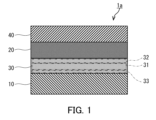
- FIG. 1 is a cross-sectional view showing an example of a capacitor according to the present disclosure.
- FIG. 2 is a cross-sectional view showing another example of a capacitor according to the present disclosure.
- FIG. 3A is a cross-sectional view showing yet another example of a capacitor according to the present disclosure.
- FIG. 3B is a cross-sectional view showing yet another example of a capacitor according to the present disclosure.
- FIG. 4A is a diagram illustrating an example of an electric circuit according to the present disclosure.
- FIG. 4B is a diagram illustrating an example of a circuit board according to the present disclosure.
- FIG. 4C is a schematic diagram illustrating an example of an apparatus of the present disclosure.
- FIG. 1 is a graph showing the relationship between the atomic ratio of fluorine (F), tantalum (Ta), and oxygen (O) and depth in a depth profile by Rutherford backscattering spectrometry (RBS) of a sample according to Example 1A.
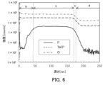
- FIG. 6 is a graph showing the relationship between the signal intensity and depth of F ⁇ , TaO 3 ⁇ , and O ⁇ in a depth profile by time-of-flight secondary ion mass spectrometry (TOF-SIMS) of the sample according to Example 1B.
- FIG. 7 is a graph showing the relationship between the signal intensity and depth of F ⁇ , TaO 3 ⁇ , and O ⁇ in the depth profile by TOF-SIMS of the sample according to Comparative Example 1.
- FIG. 8 is a graph showing the capacity ratios in Examples 2A to 2E and Comparative Example 2.
- FIG. 9 is a graph showing an XRD pattern of the dielectric film of the sample according to Reference Example 1.
- FIG. 10 is a graph showing the relationship between the signal intensity and depth of F ⁇ , TaO 3 ⁇ , and O ⁇ in the depth profile of the sample according to Reference Example 1 by TOF-SIMS.
- FIG. 11 is a graph showing the relationship between the signal intensity and depth of F ⁇ , TaO 3 ⁇ , and O ⁇ in the depth profile by TOF-SIMS of the sample according to Comparative Example 3.
- FIG. 12A is a graph showing the relationship between the capacitance of a capacitor and frequency.
- FIG. 12B is a graph showing the relationship between the capacitance of a capacitor and frequency.
- FIG. 13A is a graph showing the relationship between the dielectric tangent tan ⁇ of a capacitor and frequency.
- FIG. 13B is a graph showing the relationship between the dielectric tangent tan ⁇ of a capacitor and frequency.
- electrolytic capacitors are known as capacitors.
- a dielectric made of a thin oxide film is formed on the surface of metallic aluminum or metallic tantalum by chemical conversion treatment of aluminum or tantalum.
- electrolytic capacitors attempts have been made to increase the capacitance of the capacitor mainly by increasing the specific surface area of the dielectric. On the other hand, such attempts have limitations, and it is believed that if a dielectric material with a higher dielectric constant could be developed, the performance of the capacitor could be further improved.
- the polycrystalline TaO 2 F thin film described in Non-Patent Document 1 has a high dielectric constant. It is believed that the polycrystalline tantalum oxyfluoride has a high dielectric constant because it has a crystal state different from that of tantalum oxide Ta 2 O 5 , which increases polarization.
- the present inventors have found that tantalum oxide containing fluorine has a higher dielectric constant than tantalum oxide Ta 2 O 5 that does not contain fluorine, even if the tantalum oxide is amorphous. In this way, it is expected that the capacitance of the capacitor will be increased by using tantalum oxide containing fluorine in a capacitor. On the other hand, according to the study by the present inventors, it has been found that the capacitance of the capacitor may be reduced if a solid electrolyte is placed in contact with a film of tantalum oxide containing fluorine.
- the inventors have conducted extensive research into the configuration of a capacitor that uses fluorine-containing tantalum oxide and that suppresses the decrease in capacity caused by a solid electrolyte. As a result, they have newly discovered that a tantalum oxide film having a specific configuration is advantageous for suppressing the decrease in capacity caused by a solid electrolyte. Based on this new knowledge, the inventors have completed the capacitor disclosed herein.
- the capacitor 1a includes a metal tantalum 10, a solid electrolyte 20, and a tantalum oxide film 30.
- the tantalum oxide film 30 is disposed between the metal tantalum 10 and the solid electrolyte 20.
- the tantalum oxide film 30 includes a first portion 31 and a second portion 32.
- the tantalum oxide film 30 further includes, for example, a third portion 33.
- the first portion 31 contains fluorine.
- the second portion 32 contacts the first portion 31 at a position closer to the solid electrolyte 20 than the first portion 31 in the thickness direction of the tantalum oxide film 30.
- the tantalum oxide film 30 includes the first portion 31 that contains fluorine, and therefore tends to have a high relative dielectric constant. Therefore, the capacitor 1a tends to have a high capacitance.
- the inclusion of the second portion 32 in the tantalum oxide film 30 tends to suppress the decrease in capacitance caused by the solid electrolyte 20. Although the reason for this is unclear, it is thought that this is because the affinity between the tantalum oxide film 30 and the solid electrolyte 20 tends to be high, and the contact area between the tantalum oxide film 30 and the solid electrolyte 20 tends to be large.
- the capacitance ratio of the capacitor 1a is, for example, 83% or more.
- the capacitance ratio is C1 /C0, which is the ratio of the capacitance C1 of the capacitor 1a to the capacitance C0 before the solid electrolyte 20 is provided on the capacitor 1a .
- the capacitances C0 and C1 can be determined, for example, according to the method described in the examples.
- the dielectric layer is formed by anodizing an anode made of tantalum in an aqueous solution containing fluorine ions.
- the dielectric layer is made of tantalum oxide containing fluorine, so that the equivalent series resistance (ESR) of the electrolytic capacitor is small.
- ESR equivalent series resistance
- the ion diffusion rate of fluoride ions is more than twice the ion diffusion rate of oxide ions, and depending on the conditions of the anodization, fluorine may gather at the interface between the tantalum oxide and elemental tantalum, forming a region with a high fluorine concentration. It is believed that the dielectric tangent of the film is high due to the formation of a region with a high fluorine concentration at the interface between the tantalum oxide and elemental tantalum. On the other hand, since the tantalum oxide film 30 contains, for example, the third portion 33, the fluorine concentration at the interface between the tantalum oxide film 30 and the metal tantalum 10 is unlikely to be high. For this reason, the dielectric tangent of the capacitor 1a is likely to be low.
- the dielectric tangent of capacitor 1a is, for example, 0.20 or less at frequencies from 1 Hz to 10 kHz.
- each of the first portion 31, the second portion 32, and the third portion 33 is, for example, a layered portion.
- the boundary between the first portion 31 and the second portion 32 and the boundary between the first portion 31 and the third portion 33 in the tantalum oxide film 30 can be determined according to, for example, a depth profile by TOF-SIMS.
- a depth profile by TOF-SIMS the maximum value of the signal intensity of fluoride ions (F ⁇ ) is measured in the first portion 31.
- a pair of depths corresponding to half the maximum value are specified. Of the pair of depths, a position corresponding to a depth close to the metal tantalum 10 is determined as the boundary between the first portion 31 and the third portion 33, and a position corresponding to the other depth is determined as the boundary between the first portion 31 and the second portion 32.
- the boundary between the first portion 31 and the second portion 32 and the boundary between the first portion 31 and the third portion 33 in the tantalum oxide film 30 may be determined by Rutherford backscattering spectrometry (RBS).
- RBS Rutherford backscattering spectrometry
- the boundary between the tantalum metal 10 and the tantalum oxide film 30 can be determined according to, for example, a depth profile by TOF-SIMS.
- a depth profile For example, in the depth profile, the maximum value of the signal of tantalum oxide ions (TaO 3 ⁇ ) at the depth corresponding to the first portion 31 is identified. The depth corresponding to half the maximum value is identified, and the position corresponding to that depth is determined to be the boundary between the tantalum metal 10 and the tantalum oxide film 30.
- the boundary between the tantalum metal 10 and the tantalum oxide film 30 may also be determined by RBS.
- the depth profile of the tantalum oxide film 30 by TOF-SIMS and RBS is not limited to a specific embodiment.
- the ratio A 33F /A 31F of the average A 33F to the average A 31F is 0.5 or less.
- the average A 31F is the average value of the signal intensity of the fluoride ion (F ⁇ ) in the first portion 31.
- the average A 33F is the average value of the signal intensity of the fluoride ion (F ⁇ ) in the second portion 32.
- the ratio A 33F /A 31F may be 0.2 or less, 0.15 or less, or 0.129 or less.
- the ratio A 33F /A 31F may be, for example, 0.01 or more, 0.05 or more, or 0.1 or more.
- the ratio A 32F /A 31F of the average value A 32F to the average value A 31F is, for example, 0.9 or less.
- the average value A 32F is the average value of the signal intensity of fluoride ions (F ⁇ ) in the third portion 33. With this configuration, the capacitor 1a is more likely to have a low dielectric tangent.
- the ratio A 32F /A 31F may be 0.5 or less, 0.4 or less, or 0.379 or less.
- the ratio A 32F /A 31F may be, for example, 0.01 or more, 0.05 or more, or 0.1 or more.
- the coefficient of variation of the signal intensity of oxygen (O) or oxygen ions (O - ) in the first region 31 and the second region 32 is not limited to a specific value.
- the coefficient of variation is, for example, 0.09 or less. In this case, the variation of the signal intensity of oxygen ions (O - ) is small in the first region 31 and the second region 32, and the capacitor 1a is more likely to have a high capacitance.
- the coefficient of variation may be 0.088 or less, 0.05 or less, or 0.01 or less.
- the coefficient of variation can be determined by dividing the standard deviation by the average value.
- the thickness t 30 of the tantalum oxide film 30 is not limited to a specific value, and is, for example, not less than 1 nm and not more than 1 ⁇ m.
- the first portion 31 may be crystalline or amorphous. Even if the first portion 31 is amorphous, the tantalum oxide film 30 is likely to have a high dielectric constant, and the capacitor 1a is likely to have a high capacitance.
- the object can be determined to be amorphous when a broad halo pattern is shown in an XRD pattern using Cu-K ⁇ radiation of the object at a diffraction angle 2 ⁇ of 10° to 50°.
- the second portion 32 may be crystalline or amorphous.
- the third portion 33 may be crystalline or amorphous.
- the composition of the first portion 31 is not limited to a specific composition.
- the first portion 31 does not contain, for example, silicon and titanium.
- the first portion 31 has a composition expressed, for example, as TaO x1 F y1 . This composition satisfies, for example, the conditions of 0 ⁇ x1 ⁇ 2.5 and 0 ⁇ y1 ⁇ 0.4.
- the tantalum oxide film 30 is likely to have a high relative dielectric constant, and the capacitor 1a is likely to have a high capacitance.
- the fluorine contained in the tantalum oxide film 30 is likely to be prevented from diffusing toward the metal tantalum 10 due to the influence of an electric field, heat, and the like, and the dielectric loss tangent is likely to be low.
- the condition y1 ⁇ 0.015 is satisfied.
- the tantalum oxide film 30 is more likely to have a high relative dielectric constant, and the capacitor 1a is more likely to have a high capacitance.
- the condition y1 ⁇ 0.016, y1 ⁇ 0.017, y1 ⁇ 0.018, y1 ⁇ 0.019, y1 ⁇ 0.02, or y1 ⁇ 0.03 may be satisfied.
- y1 ⁇ 0.3 or y1 ⁇ 0.2 may also be satisfied.
- the fluorine concentration in the second portion 32 is not limited to a specific value as long as the fluorine concentration in the second portion 32 is lower than the fluorine concentration in the first portion 31.
- the second portion 32 has a composition expressed as TaO x2 F y2 . This composition satisfies, for example, the conditions 0 ⁇ x2 ⁇ 2.5 and 0 ⁇ y2 ⁇ 0.015. In this case, the capacity reduction due to the solid electrolyte is more easily suppressed.
- the fluorine concentration in the third portion 33 is not limited to a specific value as long as the fluorine concentration in the third portion 33 is lower than the fluorine concentration in the first portion 31.
- the third portion 33 has a composition expressed as TaO x3 F y3 , for example. This composition satisfies, for example, the conditions 0 ⁇ x3 ⁇ 2.5 and 0 ⁇ y3 ⁇ 0.015. In this case, the fluorine concentration near the tantalum metal 10 of the tantalum oxide film 30 is less likely to become high, and the dielectric tangent of the capacitor 1a is more likely to become low.
- the values of x1, y1, x2, y2, x3, and y3 in the above composition can be determined, for example, based on the results of RBS.
- the values of x1, y1, x2, y2, x3, and y3 may also be determined by combining TOF-SIMS with another analytical method such as RBS.
- the solid electrolyte 20 is not limited to a specific solid electrolyte.
- the solid electrolyte 20 may include, for example, a conductive polymer or a manganese compound such as manganese oxide.
- Examples of conductive polymers are polypyrrole, polythiophene, polyaniline, and derivatives thereof.
- the solid electrolyte 20 may be, for example, in the form of a layer.
- the capacitor 1a further includes, for example, a conductor 40.
- the solid electrolyte 20 is disposed between the tantalum oxide film 30 and the conductor 40 in the thickness direction of the tantalum oxide film 30.
- the material of the conductor 40 is not limited to a specific material.
- the conductor 40 may include a valve metal such as aluminum, tantalum, niobium, or bismuth, or may include a precious metal such as gold or platinum, or may include nickel.
- the conductor 40 may include a carbon material such as graphite.
- the cathode is formed by a conductor 40 and a solid electrolyte 20.
- the tantalum oxide film 30 may be formed by the following methods (I), (II), and (III).
- a voltage of several volts [V] to several hundred volts [V] is applied between the anode and the cathode with an electrolyte disposed between them.
- a voltage of 5 volts [V] to 300 volts [V] is applied.
- metal tantalum is the anode
- anions attracted toward the metal tantalum combine with ionized tantalum to form a chemical film.
- the chemical film may incorporate ions or atoms that are impurities derived from the electrolyte present around the anode.
- the second portion 32 and the third portion 33 may contain elements other than tantalum and oxygen, such as fluorine, at a concentration of 0.4% or less on an atomic number basis.
- FIG. 2 is a cross-sectional view showing another example of a capacitor of the present disclosure.
- Capacitor 1b shown in FIG. 2 is configured similarly to capacitor 1a, except for the parts that will be specifically described. Components of capacitor 1b that are the same as or correspond to the components of capacitor 1a are given the same reference numerals, and detailed descriptions are omitted. The description of capacitor 1a also applies to capacitor 1b, unless there is a technical contradiction.
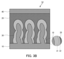
- capacitor 1b at least a portion of metal tantalum 10 is porous.
- the surface area of metal tantalum 10 tends to be large, and capacitor 1b tends to have a high capacitance.
- Such a porous structure can be formed, for example, by etching metal foil and sintering powder.
- a tantalum oxide film 30 is disposed on the surface of the porous portion of the metal tantalum 10.
- the tantalum oxide film 30 is formed, for example, by anodization.
- a solid electrolyte 20 is disposed so as to fill the voids around the porous portion of the tantalum oxide film 30.
- the cathode is formed by the conductor 40 and the solid electrolyte 20.
- the conductor 40 may include, for example, a solidified silver-containing paste, a carbon material such as graphite, or both the above-mentioned solidified material and a carbon material.
- FIGS. 3A and 3B are cross-sectional views showing yet another example of a capacitor of the present disclosure.
- Capacitor 1c shown in FIG. 3A and capacitor 1d shown in FIG. 3B are configured similarly to capacitors 1a and 1b, respectively, except for the parts that will be specifically described.
- Components of capacitor 1c or capacitor 1d that are the same as or correspond to the components of capacitor 1a or capacitor 1b are given the same reference numerals, and detailed description will be omitted.
- the descriptions of capacitor 1a and capacitor 1b also apply to capacitors 1c and 1d, unless technically inconsistent.
- tantalum oxide film 30 includes first portion 31 and second portion 32, but does not include third portion 33.
- first portion 31 is in contact with metal tantalum 10.
- tantalum oxide film 30 includes second portion 32, capacity reduction due to solid electrolyte 20 is likely to be suppressed.
- Such tantalum oxide film 30 can be produced, for example, by adjusting the conditions of anodization (III) in the method including (I), (II), and (III) above.
- such tantalum oxide film 30 can be easily obtained by increasing the voltage applied between the anode and cathode in anodization (III) above.
- FIG. 4A is a diagram showing a schematic example of an electric circuit according to the present disclosure.
- the electric circuit 3 includes a capacitor 1a.
- the electric circuit 3 may be an active circuit or a passive circuit.
- the electric circuit 3 may be a discharge circuit, a smoothing circuit, a decoupling circuit, or a coupling circuit. Since the electric circuit 3 includes the capacitor 1a, the electric circuit 3 is likely to exhibit the desired performance. For example, noise is likely to be reduced in the electric circuit 3.
- the electric circuit 3 may also include a capacitor 1b.
- FIG. 4B is a schematic diagram showing an example of a circuit board according to the present disclosure.
- the circuit board 5 includes a capacitor 1a.
- an electric circuit 3 including the capacitor 1a is formed on the circuit board 5. Since the circuit board 5 includes the capacitor 1a, the circuit board 5 is likely to exhibit the desired performance.
- the circuit board 5 may be an embedded board or a motherboard.
- the circuit board 5 may include a capacitor 1b.
- FIG. 4C is a diagram showing a schematic example of a device according to the present disclosure.
- the device 7 includes a capacitor 1a.
- the device 7 includes, for example, a circuit board 5 including the capacitor 1a. Since the device 7 includes the capacitor 1a, the device 7 is likely to exhibit the desired performance.
- the device 7 may be an electronic device, a communication device, a signal processing device, or a power supply device.
- the device 7 may be a server, an AC adapter, an accelerator, or a flat panel display such as a liquid crystal display (LCD).
- the device 7 may be a USB charger, a solid state drive (SSD), an information terminal such as a PC, a smartphone, or a tablet PC, or an Ethernet switch.
- the device 7 may include a capacitor 1b.
- Tantalum metal A solid electrolyte; a tantalum oxide film disposed between the tantalum metal and the solid electrolyte; the tantalum oxide film includes a first portion containing fluorine and a second portion in contact with the first portion at a position closer to the solid electrolyte than the first portion in a thickness direction of the tantalum oxide film, the concentration of fluorine in the second portion is lower than the concentration of fluorine in the first portion; Capacitor.
- the tantalum oxide film further includes a third portion in contact with the first portion at a position closer to the metallic tantalum than the first portion in a thickness direction of the tantalum oxide film, the concentration of fluorine in the third portion is lower than the concentration of fluorine in the first portion;
- the capacitor of claim 1 .
- the first portion is amorphous.
- the capacitor of claim 1 .
- the first portion has a composition represented by TaO x1 F y1 , The composition satisfies the conditions 0 ⁇ x1 ⁇ 2.5 and 0 ⁇ y1 ⁇ 0.4, The capacitor according to any one of the first to third aspects.
- the second portion has a composition represented by TaO x2 F y2 , The composition satisfies the conditions 0 ⁇ x2 ⁇ 2.5 and 0 ⁇ y2 ⁇ 0.015.
- the third portion has a composition represented by TaO x3 F y3 , The composition satisfies the conditions 0 ⁇ x3 ⁇ 2.5 and 0 ⁇ y3 ⁇ 0.015.
- Technique 7 In a depth profile of an element or an ion of the tantalum oxide film, a coefficient of variation of a signal intensity of oxygen (O) or an oxygen ion O ⁇ at the first site and the second site is 0.09 or less.
- a capacitor according to any one of claims 1 to 6. An electric circuit comprising the capacitor according to any one of claims 1 to 7.
- Technique 9 A circuit board comprising the capacitor according to any one of claims 1 to 7.
- Technique 10 An apparatus comprising the capacitor according to any one of claims 1 to 7.
- Example 1A A flat tantalum metal plate was immersed in acetone and ultrasonically cleaned for 10 minutes to clean the surface of the tantalum metal. The acetone adhering to the surface of the tantalum metal was then evaporated, and the surface of the tantalum metal was washed with pure water. The tantalum metal was then dried in the air to obtain an anode foil.
- the above anode foil and a platinum foil as a counter electrode were placed at a predetermined interval so as to be immersed in the phosphoric acid aqueous solution.
- the part of the anode foil that was not immersed in the aqueous solution was connected to the positive pole of a power supply device, and the part of the platinum foil that was not immersed in the aqueous solution was connected to the negative pole of the power supply device.
- a voltage of 97 V was applied between the anode foil and the platinum foil for 30 minutes, forming an oxide layer containing Ta2O5 on the surface of the anode foil.
- the anode foil was pulled out of the aqueous solution, washed with pure water, and then dried in the air.
- the above anode foil with the oxide layer formed and a platinum foil as a counter electrode were placed at a predetermined interval so as to be immersed in the NH4HF2 aqueous solution .
- the part of the anode foil that was not immersed in the aqueous solution was connected to the positive pole of a power supply device, and the part of the platinum foil that was not immersed in the aqueous solution was connected to the negative pole of the power supply device.
- a voltage of 156 V was applied between the anode foil and the platinum foil for 10 minutes to form a tantalum oxide layer containing fluorine.
- the anode foil was pulled out of the aqueous solution, washed with pure water, and then dried in the air.
- anode foil on which the oxide layer containing fluorine was formed and a platinum foil as a counter electrode were placed at a predetermined distance so as to be immersed in an aqueous phosphoric acid solution.
- the part of the anode foil not immersed in the aqueous solution was connected to the positive electrode of a power supply device, and the part of the platinum foil not immersed in the aqueous solution was connected to the negative electrode of the power supply device.
- a voltage of 187 V was applied between the anode foil and the platinum foil for 30 minutes to form an oxide layer containing Ta2O5 .
- the anode foil was pulled out of the aqueous solution, washed with pure water, and then dried in the air. In this way, a sample according to Example 1A was obtained in which a dielectric film was formed on the surface of metallic tantalum.
- Example 1B A flat tantalum metal plate was immersed in acetone and ultrasonically cleaned for 10 minutes to clean the surface of the tantalum metal. The acetone adhering to the surface of the tantalum metal was then evaporated, and the surface of the tantalum metal was washed with pure water. The tantalum metal was then dried in the air to obtain an anode foil.
- the above anode foil and a platinum foil as a counter electrode were placed at a predetermined interval so as to be immersed in the phosphoric acid aqueous solution.
- the part of the anode foil that was not immersed in the aqueous solution was connected to the positive pole of a power supply device, and the part of the platinum foil that was not immersed in the aqueous solution was connected to the negative pole of the power supply device.
- a voltage of 30 V was applied between the anode foil and the platinum foil for 13 hours, forming an oxide layer containing Ta2O5 on the surface of the anode foil.
- the anode foil was then pulled out of the aqueous solution, washed with pure water, and then dried in the air.
- the anode foil with the oxide layer formed and a platinum foil as a counter electrode were placed at a specified distance so that they were immersed in a mixed aqueous solution of NaF and sodium phosphate buffer.
- the part of the anode foil that was not immersed in the mixed aqueous solution was connected to the positive pole of a power supply, and the part of the platinum foil that was not immersed in the mixed aqueous solution was connected to the negative pole of the power supply.
- a voltage of 75 V was applied between the anode foil and the platinum foil for 4 hours, forming a fluorine-containing tantalum oxide layer.
- the concentrations of NaF and sodium phosphate buffer in the mixed aqueous solution were 0.1 mol/L and 0.05 mol/L, respectively.
- the anode foil was removed from the mixed aqueous solution, washed with pure water, and then dried in the air.
- anode foil with the oxide layer containing fluorine formed thereon and a platinum foil as a counter electrode were placed at a predetermined distance so as to be immersed in the phosphoric acid aqueous solution.
- the part of the anode foil not immersed in the aqueous solution was connected to the positive pole of a power supply device, and the part of the platinum foil not immersed in the aqueous solution was connected to the negative pole of the power supply device.
- a voltage of 90 V was applied between the anode foil and the platinum foil for 4 hours to form an oxide layer containing Ta2O5 .
- the anode foil was pulled out of the phosphoric acid aqueous solution, washed with pure water, and then dried in the air. In this way, a sample according to Example 1B was obtained in which a dielectric film was formed on the surface of metallic tantalum.
- Comparative Example 1 A sample according to Comparative Example 1 was obtained in the same manner as in Example 1B, except that the formation of an additional oxide layer using an aqueous phosphoric acid solution on the anode foil on which a fluorine-containing oxide layer was formed was omitted.
- FIG. 5 is a graph showing the relationship between the atomic ratio of fluorine (F), tantalum (Ta), and oxygen (O) and the depth in the RBS depth profile of the sample according to Example 1A.
- the vertical axis shows the atomic ratio of fluorine (F), tantalum (Ta), and oxygen (O)
- the horizontal axis shows the depth.
- the dielectric film of the sample according to Example 1A included a portion a having a relatively high concentration of F, and portions b and c having a relatively low concentration of F.
- the boundaries between the portion a and the portions b and c were determined by identifying the depth corresponding to half the maximum value of the concentration of F in the portion a. It is understood that the boundary between the portion b and the portion a is located at a position corresponding to a depth of about 80 nm.
- the boundary between the portion c and the portion a is understood to be located at a position corresponding to a depth of about 254 nm. Therefore, the thickness of the portion a is understood to be about 174 nm, and the thickness of the portion b is understood to be about 80 nm.
- the boundary between the dielectric film and the metal tantalum was determined by identifying the depth corresponding to the half-maximum of the signal intensity of TaO 3- at the portion a. It was suggested that the boundary between the dielectric film and the metal tantalum is located at a position corresponding to a depth of about 300 nm. Therefore, the thickness of the portion c is understood to be about 46 nm. No increase in fluorine concentration was confirmed at the boundary between the dielectric film and the metal tantalum. According to the obtained RBS spectrum, the compositions of the portion a of the dielectric layer of the samples according to Example 1A and Example 1B were TaO 2.33 F 0.19 and TaO 2.27 F 0.03 , respectively.
- compositions of the portion b of the dielectric layer of the samples according to Example 1A and Example 1B were TaO 2.47 and TaO 2.48 , respectively.
- the elemental fluorine concentrations in portion b of the samples according to Examples 1A and 1B were lower than the analytical lower limit of 0.4 mass%, and in the composition represented by TaO x2 F y2 , y2 ⁇ 0.015.
- the elemental fluorine concentrations in portion c of the samples according to Examples 1A and 1B were lower than the analytical lower limit of 0.4 mass%, and in the composition represented by TaO x3 F y3 , y3 ⁇ 0.015.
- the dielectric films of the samples of Example 1A and Example 1B have portion b, and therefore, in comparison with Examples 2A to 2E and Comparative Example 2 described below, it is believed that the reduction in capacity due to the solid electrolyte is more easily suppressed than in the sample of Comparative Example 1.
- the samples of Example 1A and Example 1B have portion c, it is believed that the dielectric tangent of the capacitor is easily reduced according to Reference Example 1 described below.
- TOF-SIMS Fragments of a predetermined size were cut out from the samples according to Example 1B and Comparative Example 1, and samples for TOF-SIMS were prepared by embedding them in resin.
- the samples prepared from the samples according to Example 1B and Comparative Example 1 were subjected to TOF-SIMS to perform composition analysis in the depth direction of the dielectric film.
- the sputtering ion species used was O 2 + .
- FIG. 6 shows fluoride ions (F ⁇ ), tantalate ions (TaO 3 ⁇ ), and 7 is a graph showing the relationship between the signal intensity of oxygen ions (O ⁇ ) and the depth.
- FIG. 6 shows fluoride ions (F ⁇ ), tantalate ions (TaO 3 ⁇ ), and 7 is a graph showing the relationship between the signal intensity of oxygen ions (O ⁇ ) and the depth.
- FIG. 7 is a graph showing the relationship between the signal intensity of F ⁇ , tantalate ions TaO 3 ⁇ , and O 1 is a graph showing the relationship between signal intensity and depth. 6 and 7, the vertical axis indicates the signal intensity of each ion, and the horizontal axis indicates the depth in the dielectric film.
- the dielectric film of the sample according to Example 1B included a portion a where the signal intensity of F ⁇ was relatively high, and portions b and c where the signal intensity of F ⁇ was relatively low.
- the boundary between the portion a and the portions b and c was determined by identifying a depth corresponding to half the maximum value of the signal intensity of F ⁇ at the portion a.
- the boundary between the portion b and the portion a is understood to be located at a position corresponding to a depth of about 43 nm.
- the boundary between the portion c and the portion a is understood to be located at a position corresponding to a depth of about 170 nm.
- the thickness of the portion a is about 127 nm, and the thickness of the portion b is about 43 nm.
- the boundary between the dielectric film and the metal tantalum was determined by identifying a depth corresponding to half the maximum value of the signal intensity of TaO 3 ⁇ at the portion a. It was suggested that the boundary between the dielectric film and the metal tantalum is located at a position corresponding to a depth of about 176 nm. Therefore, it is understood that the thickness of the portion c is about 6 nm. No increase in fluorine concentration was confirmed at the boundary between the dielectric film and the metal tantalum.
- the dielectric film of the sample according to Comparative Example 1 is understood to exist from its surface to a depth of about 180 nm.
- the fluorine concentration was almost constant from the surface of the dielectric film to a depth of about 170 nm.
- Example 2A One end of a rod-shaped anode lead made of metallic tantalum was embedded in the metallic tantalum powder, and the tantalum powder was molded into a rectangular solid to obtain a compact. The compact was sintered to obtain an anode body having a porous structure in which one end of the anode lead was embedded.
- the anode body was immersed in an aqueous phosphoric acid solution, and a voltage of 40 V was applied to the anode body using an anode lead for 13 hours to form an oxide layer containing Ta2O5 on the surface of the anode body.
- the anode body was removed from the aqueous phosphoric acid solution, washed with pure water, and then dried in a drying furnace adjusted to 100°C for 10 minutes.
- the anode body with the oxide layer formed thereon was immersed in an aqueous NH4HF2 solution , and a voltage of 80 V was applied to the anode body for 10 minutes using an anode lead, thereby forming a fluorine-containing tantalum oxide layer on the surface of the anode body.
- the above anode body on which the fluorine-containing oxide layer was formed was immersed in an aqueous phosphoric acid solution, and a voltage of 80 V was applied to the anode body using an anode lead for 30 minutes to form an oxide layer containing Ta2O5 .
- the anode body was removed from the aqueous phosphoric acid solution, washed with pure water, and then dried for 10 minutes in a drying furnace adjusted to 100°C. In this manner, 100 anode bodies with a dielectric film according to Example 2A were obtained, in which a dielectric film was formed on the surface of the anode body.
- a solid electrolyte layer containing polythiophene was formed on the dielectric film surface of 50 anode bodies with dielectric film according to Example 2A using a chemical polymerization method.
- Example 2A the capacitor of Example 2A was produced.
- Example 2B An anode body prepared by sintering a compact of tantalum powder in the same manner as in Example 1A was immersed in an aqueous phosphoric acid solution, and a voltage of 30 V was applied to the anode body for 13 hours using an anode lead to form an oxide layer containing Ta2O5 on the surface of the anode body. The anode body was removed from the aqueous phosphoric acid solution and washed with pure water, and then dried for 10 minutes in a drying furnace adjusted to 100°C.
- the anode body with the oxide layer formed was immersed in a mixed solution of NaF and sodium phosphate buffer, and 83 V was applied to the anode body using the anode lead for 4 hours. This formed a fluorine-containing tantalum oxide layer on the surface of the anode body.
- the above anode body on which the fluorine-containing oxide layer was formed was immersed in an aqueous phosphoric acid solution, and a voltage of 88 V was applied to the anode body using an anode lead for 4 hours to form an oxide layer containing Ta2O5 .
- the anode body was removed from the aqueous phosphoric acid solution, washed with pure water, and then dried for 10 minutes in a drying furnace adjusted to 100°C. In this manner, 100 anode bodies with a dielectric film according to Example 2B were obtained, in which a dielectric film was formed on the surface of the anode body.
- Example 2B a solid electrolyte layer, a carbon-containing layer, and a silver-containing layer were formed on the dielectric film surface of 50 anode bodies with a dielectric film according to Example 2B. In this manner, the capacitor according to Example 2B was produced.
- Example 2C to 2E Dielectric film-coated anode bodies according to Examples 2C, 2D, and 2E were obtained in the same manner as in Example 2B, except that the voltage applied to the anode body in forming the fluorine-containing oxide layer was changed to 78 V, 73 V, and 68 V. The number of dielectric film-coated anode bodies according to Examples 2C, 2D, and 2E obtained was 100. Fifty capacitors according to Examples 2C, 2D, and 2E were produced in the same manner as in Example 2B, except that fifty dielectric film-coated anode bodies according to Examples 2C, 2D, and 2E were used instead of the fifty dielectric film-coated anode bodies according to Example 2B.
- An anode body with a dielectric film according to Comparative Example 2 was obtained in the same manner as in Example 2B, except that the voltage applied to the anode body in the formation of the fluorine-containing oxide layer was changed to 88 V and the subsequent formation of a further oxide layer using an aqueous phosphoric acid solution was omitted.
- the number of anode bodies with a dielectric film according to Comparative Example 2 obtained was 100.
- a capacitor according to Comparative Example 2 was produced in the same manner as in Example 2B, except that 50 anode bodies with a dielectric film according to Comparative Example 2 were used instead of the 50 anode bodies with a dielectric film according to Example 2B.
- Example 2A As shown in Table 1, the capacitances of the capacitors according to Example 2A, Example 2B, Example 2C, Example 2D, Example 2E, and Comparative Example 2 were lower than the capacitances of the anode bodies with dielectric film according to Example 2A, Example 2B, Example 2C, Example 2D, Example 2E, and Comparative Example 2, respectively. This suggests that the solid electrolyte is not in contact with the entire dielectric film.
- the capacity ratios in Examples 2A to 2E were 83% or more, which was higher than the capacity ratio in Comparative Example 2. This is probably because the affinity of the further oxide layer formed using an aqueous phosphoric acid solution for the anode body on which the oxide layer containing fluorine was formed with the solid electrolyte was high, and the contact area between the dielectric film and the solid electrolyte was increased. As shown in FIG. 8, it was confirmed that the capacity ratio tends to be higher when the voltage applied to the anode body in forming the oxide layer containing fluorine is low.
- the ratio of the thickness of the further oxide layer formed using an aqueous phosphoric acid solution for the anode body on which the oxide layer containing fluorine was formed to the thickness of the dielectric film becomes large when the voltage applied to the anode body in forming the oxide layer containing fluorine is low.
- the capacity ratio is likely to be high when the voltage applied to the anode body in forming the oxide layer containing fluorine is low.
- ⁇ Reference Example 1> A flat metal tantalum plate was immersed in acetone and ultrasonically cleaned for 10 minutes to clean the surface of the metal tantalum. The acetone adhering to the surface of the metal tantalum was then evaporated, the surface of the metal tantalum was washed with pure water, and the metal tantalum was then dried in the air.
- the above metal tantalum and platinum foil as a counter electrode were placed at a specified distance so that they were immersed in the phosphoric acid aqueous solution.
- the part of the metal tantalum that was not immersed in the aqueous solution was connected to the positive pole of a power supply, and the part of the platinum foil that was not immersed in the aqueous solution was connected to the negative pole of the power supply.
- a current was applied from the power supply in a constant voltage state, and a voltage of 64 V was applied between the metal tantalum and the counter electrode for 30 minutes. This caused an electrochemical reaction on the surface of the metal tantalum, which was the anode, and an oxide film was obtained.
- the metal tantalum with the oxide film formed was removed from the aqueous solution, washed with pure water, and dried in the air.
- the above - mentioned metal tantalum on which the oxide film was formed was used as an anode, and platinum foil was used as a cathode, so that they were immersed in the NH4HF2 aqueous solution, and the parts of the anode and cathode that were not immersed in the aqueous solution were connected to the positive and negative electrodes of a power supply device, respectively.
- a current was applied from the power supply device in a constant voltage state, and a voltage of 80 V was applied between the anode and the cathode for 10 minutes, to perform anodization. Thereafter, the anode after the anodization was removed from the aqueous solution, washed with pure water, and dried. In this way, a sample according to Reference Example 1 in which a dielectric film was formed on the surface of the metal tantalum was obtained.
- the metal tantalum was used as an anode and the platinum foil was used as a cathode, so that they were immersed in the NH4HF2 aqueous solution, and the anode and cathode parts not immersed in the aqueous solution were connected to the positive and negative electrodes of a power supply device, respectively.
- a current was applied from the power supply device in a constant voltage state, and a voltage of 80 V was applied between the anode and the cathode for 10 minutes to perform anodization.
- the anode after the anodization was taken out of the aqueous solution, washed with pure water, and dried. In this way, a sample according to Comparative Example 3 in which a dielectric film was formed on the surface of the metal tantalum was obtained.
- tantalum metal and platinum foil as a counter electrode were placed at a specified distance so as to be immersed in the phosphoric acid aqueous solution.
- the part of the tantalum metal that was not immersed in the aqueous solution was connected to the positive electrode of a power supply device, and the part of the platinum foil that was not immersed in the aqueous solution was connected to the negative electrode of the power supply device.
- a current was applied from the power supply device in a constant voltage state, and a voltage of 80 V was applied between the tantalum metal and the counter electrode for 30 minutes.
- An electrochemical reaction was caused to occur on the surface of the tantalum metal, which was the anode, to obtain an oxide film.
- FIG. 9 shows the XRD pattern of the dielectric film of the sample according to Reference Example 1. No peaks derived from a crystal structure were confirmed in the XRD pattern shown in FIG. 9, indicating that the tantalum oxide film of the sample according to Reference Example 1 is amorphous.
- TOF-SIMS Fragments of a predetermined size were cut out from the samples according to Reference Example 1 and Comparative Example 3, and were embedded in resin to prepare samples for TOF-SIMS.
- the samples prepared from the samples according to Reference Example 1 and Comparative Example 3 were subjected to TOF-SIMS to perform a composition analysis of the oxide film of the dielectric film in the depth direction.
- a Bi beam was used.
- O 2 + was used as the sputtering ion species.
- FIG. 10 shows the signal intensities and depths of F ⁇ , TaO 3 ⁇ , and O ⁇ in the depth profile of the sample according to Reference Example 1 by TOF-SIMS.
- FIG. 11 is a graph showing the relationship between the signal intensity and the depth of F ⁇ , TaO 3 ⁇ , and O ⁇ in the depth profile of the sample according to Comparative Example 3 by TOF-SIMS. . 10 and 11, the vertical axis indicates the signal intensity of each ion, and the horizontal axis indicates the depth in the dielectric film.
- the dielectric film of the sample according to Reference Example 1 is formed on metallic tantalum and includes a portion with a high fluorine concentration and a portion with a low fluorine concentration.
- the portion with a high fluorine concentration exists from the surface of the dielectric film to a depth of about 60 nm.
- the portion with a low fluorine concentration exists from a depth of about 75 nm to a depth of about 150 nm in the dielectric film. From the signal intensity of F ⁇ in the portion with a low fluorine concentration of the dielectric film, it is understood that the fluorine concentration in this portion is 0.4% or less on the basis of the number of atoms.
- the variation in the fluorine concentration in each of the portion with a high fluorine concentration and the portion with a low fluorine concentration is small.
- the depth of about 150 nm or more corresponds to metallic tantalum. No increase in the fluorine concentration is confirmed at the boundary between metallic tantalum and the dielectric film.
- the dielectric film of the sample according to Comparative Example 3 exists from its surface to a depth of about 180 nm.
- an increase in the fluorine concentration is confirmed at the boundary between the metal tantalum and the dielectric film. This is thought to be because the diffusion rate of fluoride ions is much faster than the diffusion rate of oxide ions, and therefore diffusion of fluoride ions into the metal tantalum and generation of tantalum fluoride occurred prior to the formation of the tantalum oxide film by anodization.
- the tantalum fluoride thus generated has poor electrical insulation properties and may reduce the dielectric properties required for a capacitor.
- tantalum fluoride near the metal tantalum may cause the formation of the tantalum oxide film to be non-uniform, which may cause peeling of the tantalum oxide film. For this reason, it is difficult to say that a dielectric in which tantalum fluoride exists near the metal tantalum is suitable as a dielectric for a capacitor.
- a chemical conversion treatment is performed in advance using a solution that does not contain fluorine, as in Reference Example 1, a tantalum oxide film containing fluorine can be easily formed on the metal tantalum without peeling.
- Figure 12A is an enlarged view of the part surrounded by the two-dot chain line in Figure 12B.
- Figures 13A and 13B are graphs showing the relationship between the dielectric loss tangent tan ⁇ of the capacitor and the frequency.
- the vertical axis indicates tan ⁇
- the horizontal axis indicates the frequency.
- FIG. 13A is an enlarged view of the area surrounded by the two-dot chain line in FIG. 13B.
- the dielectric layers of the samples according to Reference Example 1, Comparative Example 3, and Comparative Example 4 are formed on metal tantalum with the same surface state, and it is understood that there is no significant difference in the surface area of the dielectric layer of each sample.
- the capacitances of the capacitors according to Reference Example 1 and Comparative Example 3 are higher than the capacitance of the capacitor according to Comparative Example 4.
- the capacitance of the capacitor according to Comparative Example 3 is high, as shown in Figures 13A and 13B, the dielectric tangent tan ⁇ of the capacitor according to Comparative Example 3 is high. Tan ⁇ corresponds to the energy consumed inside the capacitor, and it is understood that the capacitor according to Comparative Example 3 has a large loss of electrical energy.
- the capacitor according to Reference Example 1 is not only high in capacitance, but also has a low dielectric tangent tan ⁇ , and is superior in terms of low electrical energy loss.
- Example 1A The correspondence between Example 1A, Example 1B, Examples 2A to 2E, Reference Example 1, and Comparative Examples 1 to 4 is shown in Table 2.
- the capacitor disclosed herein is advantageous in terms of suppressing the loss of capacity due to the solid electrolyte.
Landscapes
- Engineering & Computer Science (AREA)
- Power Engineering (AREA)
- Microelectronics & Electronic Packaging (AREA)
- Chemical & Material Sciences (AREA)
- Chemical Kinetics & Catalysis (AREA)
- Electrochemistry (AREA)
- Materials Engineering (AREA)
- Manufacturing & Machinery (AREA)
- Fixed Capacitors And Capacitor Manufacturing Machines (AREA)
- Electric Double-Layer Capacitors Or The Like (AREA)
Priority Applications (4)
| Application Number | Priority Date | Filing Date | Title |
|---|---|---|---|
| JP2025524891A JPWO2024248112A1 (https=) | 2023-06-01 | 2024-05-30 | |
| CN202480035785.8A CN121285869A (zh) | 2023-06-01 | 2024-05-30 | 电容器、电路、电路板和设备 |
| KR1020257037504A KR20260016472A (ko) | 2023-06-01 | 2024-05-30 | 캐패시터, 전기 회로, 회로 기판 및 기기 |
| US19/401,919 US20260081081A1 (en) | 2023-06-01 | 2025-11-26 | Capacitor, electric circuit, circuit board, and apparatus |
Applications Claiming Priority (2)
| Application Number | Priority Date | Filing Date | Title |
|---|---|---|---|
| JP2023-090835 | 2023-06-01 | ||
| JP2023090835 | 2023-06-01 |
Related Child Applications (1)
| Application Number | Title | Priority Date | Filing Date |
|---|---|---|---|
| US19/401,919 Continuation US20260081081A1 (en) | 2023-06-01 | 2025-11-26 | Capacitor, electric circuit, circuit board, and apparatus |
Publications (1)
| Publication Number | Publication Date |
|---|---|
| WO2024248112A1 true WO2024248112A1 (ja) | 2024-12-05 |
Family
ID=93657612
Family Applications (1)
| Application Number | Title | Priority Date | Filing Date |
|---|---|---|---|
| PCT/JP2024/019959 Ceased WO2024248112A1 (ja) | 2023-06-01 | 2024-05-30 | キャパシタ、電気回路、回路基板、及び機器 |
Country Status (6)
| Country | Link |
|---|---|
| US (1) | US20260081081A1 (https=) |
| JP (1) | JPWO2024248112A1 (https=) |
| KR (1) | KR20260016472A (https=) |
| CN (1) | CN121285869A (https=) |
| TW (1) | TW202514671A (https=) |
| WO (1) | WO2024248112A1 (https=) |
Cited By (1)
| Publication number | Priority date | Publication date | Assignee | Title |
|---|---|---|---|---|
| WO2026018507A1 (ja) * | 2024-07-18 | 2026-01-22 | パナソニックIpマネジメント株式会社 | キャパシタ、電気回路、回路基板、及び機器 |
Citations (3)
| Publication number | Priority date | Publication date | Assignee | Title |
|---|---|---|---|---|
| JPH02276215A (ja) * | 1989-04-18 | 1990-11-13 | Matsushita Electric Ind Co Ltd | 固体電解コンデンサの製造方法 |
| JPH10135080A (ja) * | 1996-10-31 | 1998-05-22 | Matsushita Electric Ind Co Ltd | 固体電解コンデンサ及びその製造方法 |
| JP2006270052A (ja) * | 2005-02-23 | 2006-10-05 | Sanyo Electric Co Ltd | 固体電解コンデンサ及びその製造方法 |
Family Cites Families (1)
| Publication number | Priority date | Publication date | Assignee | Title |
|---|---|---|---|---|
| JP4383227B2 (ja) | 2004-03-31 | 2009-12-16 | 三洋電機株式会社 | 固体電解コンデンサおよびその製造方法 |
-
2024
- 2024-05-30 WO PCT/JP2024/019959 patent/WO2024248112A1/ja not_active Ceased
- 2024-05-30 CN CN202480035785.8A patent/CN121285869A/zh active Pending
- 2024-05-30 JP JP2025524891A patent/JPWO2024248112A1/ja active Pending
- 2024-05-30 KR KR1020257037504A patent/KR20260016472A/ko active Pending
- 2024-05-31 TW TW113120247A patent/TW202514671A/zh unknown
-
2025
- 2025-11-26 US US19/401,919 patent/US20260081081A1/en active Pending
Patent Citations (3)
| Publication number | Priority date | Publication date | Assignee | Title |
|---|---|---|---|---|
| JPH02276215A (ja) * | 1989-04-18 | 1990-11-13 | Matsushita Electric Ind Co Ltd | 固体電解コンデンサの製造方法 |
| JPH10135080A (ja) * | 1996-10-31 | 1998-05-22 | Matsushita Electric Ind Co Ltd | 固体電解コンデンサ及びその製造方法 |
| JP2006270052A (ja) * | 2005-02-23 | 2006-10-05 | Sanyo Electric Co Ltd | 固体電解コンデンサ及びその製造方法 |
Cited By (1)
| Publication number | Priority date | Publication date | Assignee | Title |
|---|---|---|---|---|
| WO2026018507A1 (ja) * | 2024-07-18 | 2026-01-22 | パナソニックIpマネジメント株式会社 | キャパシタ、電気回路、回路基板、及び機器 |
Also Published As
| Publication number | Publication date |
|---|---|
| JPWO2024248112A1 (https=) | 2024-12-05 |
| CN121285869A (zh) | 2026-01-06 |
| KR20260016472A (ko) | 2026-02-03 |
| US20260081081A1 (en) | 2026-03-19 |
| TW202514671A (zh) | 2025-04-01 |
Similar Documents
| Publication | Publication Date | Title |
|---|---|---|
| US20250087426A1 (en) | Capacitor, electric circuit, circuit board, apparatus, and method for manufacturing capacitor | |
| US20260081081A1 (en) | Capacitor, electric circuit, circuit board, and apparatus | |
| JP2015073015A (ja) | 電極箔、電解コンデンサおよび電極箔の製造方法 | |
| US8377148B2 (en) | Method for producing capacitor, capacitor, wiring board, electronic device, and IC card | |
| WO2022224561A1 (ja) | 誘電体、キャパシタ、電気回路、回路基板、及び機器 | |
| US8749954B2 (en) | Electrode foil and capacitor using same | |
| JP7660291B1 (ja) | 誘電体、キャパシタ、電気回路、回路基板、機器、及び誘電体の製造方法 | |
| WO2026018507A1 (ja) | キャパシタ、電気回路、回路基板、及び機器 | |
| WO2022230432A1 (ja) | 誘電体、キャパシタ、電気回路、回路基板、及び機器 | |
| US20260045416A1 (en) | Multilayer body, capacitor, electric circuit, circuit board, device, and method for producing multilayer body | |
| CN121970134A (zh) | 电容器、电路、电路板以及设备 | |
| WO2026018504A1 (ja) | キャパシタ、電気回路、回路基板、機器、及びキャパシタの製造方法 | |
| WO2026018505A1 (ja) | 誘電体、積層体、キャパシタ、電気回路、回路基板、及び機器 | |
| JP7122617B1 (ja) | 誘電体、キャパシタ、電気回路、回路基板、及び機器 | |
| WO2025238903A1 (ja) | 積層体、キャパシタ、電気回路、回路基板、機器、及び積層体の製造方法 | |
| US20260120963A1 (en) | Dielectric body, capacitor, electric circuit, circuit board, and device | |
| US20040068850A1 (en) | Chemical conversion film of tantalum or niobium, method for forming the same and electrolytic capacitor using the same | |
| JP7784633B2 (ja) | キャパシタ用部材の製造方法、キャパシタ、電気回路、回路基板、機器、及び蓄電デバイス | |
| KR20150045051A (ko) | 적층형 알루미늄 캐패시터용 전극박의 제조방법 | |
| CN121970133A (zh) | 层叠体、电容器、电气电路、电路基板、设备和层叠体的制造方法 | |
| JP2024094933A (ja) | 誘電体、それを含むキャパシタ、およびキャパシタを備える機器 | |
| CN121942056A (zh) | 电容器、电路、电路板、设备以及电容器的制造方法 | |
| JPWO2023234343A5 (https=) |
Legal Events
| Date | Code | Title | Description |
|---|---|---|---|
| 121 | Ep: the epo has been informed by wipo that ep was designated in this application |
Ref document number: 24815592 Country of ref document: EP Kind code of ref document: A1 |
|
| ENP | Entry into the national phase |
Ref document number: 2025524891 Country of ref document: JP Kind code of ref document: A |
|
| NENP | Non-entry into the national phase |
Ref country code: DE |