WO2024247534A1 - フィルタ回路およびフィルタ装置 - Google Patents
フィルタ回路およびフィルタ装置 Download PDFInfo
- Publication number
- WO2024247534A1 WO2024247534A1 PCT/JP2024/015439 JP2024015439W WO2024247534A1 WO 2024247534 A1 WO2024247534 A1 WO 2024247534A1 JP 2024015439 W JP2024015439 W JP 2024015439W WO 2024247534 A1 WO2024247534 A1 WO 2024247534A1
- Authority
- WO
- WIPO (PCT)
- Prior art keywords
- electrode
- capacitor
- terminal
- resonator
- inductor
- Prior art date
- Legal status (The legal status is an assumption and is not a legal conclusion. Google has not performed a legal analysis and makes no representation as to the accuracy of the status listed.)
- Ceased
Links
Images


Classifications
-
- H—ELECTRICITY
- H03—ELECTRONIC CIRCUITRY
- H03H—IMPEDANCE NETWORKS, e.g. RESONANT CIRCUITS; RESONATORS
- H03H7/00—Multiple-port networks comprising only passive electrical elements as network components
- H03H7/01—Frequency selective two-port networks
- H03H7/0115—Frequency selective two-port networks comprising only inductors and capacitors
-
- H—ELECTRICITY
- H01—ELECTRIC ELEMENTS
- H01F—MAGNETS; INDUCTANCES; TRANSFORMERS; SELECTION OF MATERIALS FOR THEIR MAGNETIC PROPERTIES
- H01F17/00—Fixed inductances of the signal type
- H01F17/0006—Printed inductances
- H01F17/0013—Printed inductances with stacked layers
-
- H—ELECTRICITY
- H01—ELECTRIC ELEMENTS
- H01F—MAGNETS; INDUCTANCES; TRANSFORMERS; SELECTION OF MATERIALS FOR THEIR MAGNETIC PROPERTIES
- H01F27/00—Details of transformers or inductances, in general
-
- H—ELECTRICITY
- H01—ELECTRIC ELEMENTS
- H01F—MAGNETS; INDUCTANCES; TRANSFORMERS; SELECTION OF MATERIALS FOR THEIR MAGNETIC PROPERTIES
- H01F27/00—Details of transformers or inductances, in general
- H01F27/28—Coils; Windings; Conductive connections
- H01F27/2804—Printed windings
-
- H—ELECTRICITY
- H01—ELECTRIC ELEMENTS
- H01G—CAPACITORS; CAPACITORS, RECTIFIERS, DETECTORS, SWITCHING DEVICES, LIGHT-SENSITIVE OR TEMPERATURE-SENSITIVE DEVICES OF THE ELECTROLYTIC TYPE
- H01G4/00—Fixed capacitors; Processes of their manufacture
- H01G4/30—Stacked capacitors
-
- H—ELECTRICITY
- H01—ELECTRIC ELEMENTS
- H01P—WAVEGUIDES; RESONATORS, LINES, OR OTHER DEVICES OF THE WAVEGUIDE TYPE
- H01P1/00—Auxiliary devices
- H01P1/20—Frequency-selective devices, e.g. filters
- H01P1/201—Filters for transverse electromagnetic waves
- H01P1/205—Comb or interdigital filters; Cascaded coaxial cavities
-
- H—ELECTRICITY
- H03—ELECTRONIC CIRCUITRY
- H03H—IMPEDANCE NETWORKS, e.g. RESONANT CIRCUITS; RESONATORS
- H03H7/00—Multiple-port networks comprising only passive electrical elements as network components
- H03H7/01—Frequency selective two-port networks
- H03H7/09—Filters comprising mutual inductance
-
- H—ELECTRICITY
- H03—ELECTRONIC CIRCUITRY
- H03H—IMPEDANCE NETWORKS, e.g. RESONANT CIRCUITS; RESONATORS
- H03H7/00—Multiple-port networks comprising only passive electrical elements as network components
- H03H7/01—Frequency selective two-port networks
- H03H7/17—Structural details of sub-circuits of frequency selective networks
- H03H7/1708—Comprising bridging elements, i.e. elements in a series path without own reference to ground and spanning branching nodes of another series path
-
- H—ELECTRICITY
- H01—ELECTRIC ELEMENTS
- H01F—MAGNETS; INDUCTANCES; TRANSFORMERS; SELECTION OF MATERIALS FOR THEIR MAGNETIC PROPERTIES
- H01F17/00—Fixed inductances of the signal type
- H01F17/0006—Printed inductances
- H01F17/0013—Printed inductances with stacked layers
- H01F2017/0026—Multilayer LC-filter
-
- H—ELECTRICITY
- H01—ELECTRIC ELEMENTS
- H01F—MAGNETS; INDUCTANCES; TRANSFORMERS; SELECTION OF MATERIALS FOR THEIR MAGNETIC PROPERTIES
- H01F27/00—Details of transformers or inductances, in general
- H01F27/28—Coils; Windings; Conductive connections
- H01F27/2804—Printed windings
- H01F2027/2809—Printed windings on stacked layers
-
- H—ELECTRICITY
- H03—ELECTRONIC CIRCUITRY
- H03H—IMPEDANCE NETWORKS, e.g. RESONANT CIRCUITS; RESONATORS
- H03H1/00—Constructional details of impedance networks whose electrical mode of operation is not specified or applicable to more than one type of network
- H03H2001/0021—Constructional details
- H03H2001/0085—Multilayer, e.g. LTCC, HTCC, green sheets
Definitions
- the present disclosure relates to a filter circuit and a filter device, and more specifically to a technique for improving the attenuation characteristics of a bandpass filter.
- WO 2022/071191 discloses a bandpass filter including four LC resonators.
- the bandpass filter disclosed in WO 2022/071191 discloses a configuration in which four resonators are arranged in series in one direction from the input terminal to the output terminal inside a dielectric laminate, and a configuration in which the resonators are arranged so as to form a substantially C-shaped signal path from the input terminal to the output terminal.
- an attenuation pole can be generated by forming a coupling between the resonators that bypasses the series path of the resonators from the input terminal to the output terminal, i.e., a "cross-coupling.”
- the number of attenuation poles generated by "jump coupling” is determined by the difference in the number of resonators between the main path, in which the signal to be transmitted passes through all resonators, and the sub-path, in which the signal is transmitted by skipping some of the resonators. Therefore, in principle, to generate two attenuation poles by jump coupling, it is necessary to arrange four or more stages of resonators.
- the bandpass filters are sometimes used in small communication devices such as mobile phones and smartphones, but such devices are required to be even smaller and thinner, which in turn requires that the bandpass filters themselves be made smaller.
- One way to miniaturize a bandpass filter is to reduce the number of resonators contained in the filter. However, with fewer than four resonators, the difference in the number of resonators in the cross-coupling becomes 1, making it impossible to form attenuation poles on both sides of the passband using cross-coupling.
- the present disclosure has been made to solve these problems, and its purpose is to create attenuation poles on both sides of the passband in a filter circuit having three resonators so that it functions as a bandpass filter.
- the filter circuit according to the first aspect of the present disclosure includes a first terminal, a second terminal, a ground terminal, a first resonator connected to the first terminal, a second resonator, and a third resonator connected to the second terminal.
- the second resonator is coupled to the first resonator and the third resonator.
- the first resonator and the third resonator are magnetically coupled to each other and are capacitively coupled to each other.
- the first resonator includes a first inductor and a first capacitor connected in parallel between the first terminal and the ground terminal.
- the third resonator includes a second inductor and a second capacitor connected in parallel between the second terminal and the ground terminal.
- the second resonator includes a third inductor having a first end and a second end, a third capacitor having one end connected to the first end of the third inductor, and a fourth capacitor having one end connected to the second end of the third inductor.
- a filter device includes a laminate, an input terminal, an output terminal, a ground terminal connected to the ground terminal, first to seventh capacitor electrodes, first to third plate electrodes, and first to third vias.
- the laminate is formed by stacking a plurality of dielectric layers and has a first surface and a second surface that face each other.
- the input terminal, the output terminal, and the ground terminal are disposed on the second surface of the laminate.
- the first capacitor electrode is connected to the input terminal, and at least a portion of the first capacitor electrode overlaps with the ground electrode when viewed in a plan view from the normal direction of the first surface.
- the first plate electrode is connected to the first capacitor electrode.
- the second capacitor electrode is connected to the output terminal, and at least a portion of the second capacitor electrode overlaps with the ground electrode when viewed in a plan view from the normal direction of the first surface.
- the second plate electrode is connected to the second capacitor electrode and is disposed in the same dielectric layer as the first plate electrode.
- the first via is connected to the first plate electrode and the second plate electrode, and is also connected to the ground electrode.
- the third plate electrode is disposed on the same dielectric layer as the first plate electrode and the second plate electrode, and is magnetically coupled to the first plate electrode and the second plate electrode.
- the second via and the third via are connected to the third plate electrode.
- the third capacitor electrode is connected to the second via, and at least a portion of the third capacitor electrode overlaps with the ground electrode when viewed from the normal direction of the first surface.
- the fourth capacitor electrode is connected to the third via, and at least a portion of the fourth capacitor electrode overlaps with the ground electrode when viewed from the normal direction of the first surface.
- the fifth capacitor electrode at least a portion of the fifth capacitor electrode overlaps with the first capacitor electrode and the second capacitor electrode when viewed from the normal direction of the first surface.
- the sixth capacitor electrode at least a portion of the sixth capacitor electrode overlaps with the first capacitor electrode and the third capacitor electrode when viewed from the normal direction of the first surface.
- the seventh capacitor electrode at least a portion of the seventh capacitor electrode overlaps with the second capacitor electrode and the fourth capacitor electrode when viewed from the normal direction of the first surface.
- a filter device includes a laminate, an input terminal, an output terminal, a ground electrode, and first to sixth electrodes.
- the laminate is formed by stacking a plurality of dielectric layers and has a first surface and a second surface that face each other.
- the input terminal, the output terminal, and the ground electrode are disposed on the second surface of the laminate.
- the first electrode is disposed so that at least a portion of the first electrode overlaps with the ground electrode when viewed in a plan view from the normal direction of the first surface, and is connected to the input terminal.
- the second electrode is disposed on the same dielectric layer as the first electrode so that at least a portion of the second electrode overlaps with the ground electrode when viewed in a plan view from the normal direction of the first surface, and is connected to the output terminal.
- the third electrode is adjacent to the first electrode and the second electrode, and is disposed so that at least a portion of the third electrode overlaps with the ground electrode when viewed in a plan view from the normal direction of the first surface.
- the fourth electrode connects the first electrode and the second electrode.
- the fifth electrode is disposed so that at least a portion of the fifth electrode overlaps with the first electrode and the third electrode when viewed in a plan view from the normal direction of the first surface.
- the sixth electrode is arranged so that at least a portion of it overlaps with the second electrode and the third electrode when viewed in a plan view from the normal direction of the first surface.
- the first electrode and the second electrode each face each other at a distance and have a region that is capacitively coupled.
- two resonators (a first resonator and a third resonator) connected to the input terminal and the output terminal, respectively, are magnetically and capacitively coupled, and further, the second resonator in the middle stage is configured as a so-called "open-ended" resonator in which a capacitor is connected to both ends of an inductor.
- FIG. 1 is a block diagram of a communication device having a high-frequency front-end circuit to which a filter device according to a first embodiment is applied.
- 1 is an equivalent circuit diagram of a filter device according to a first embodiment.
- 1 is an external perspective view of a filter device according to a first embodiment;
- FIG. 4 is an exploded perspective view showing an example of a laminated structure of the filter device of FIG. 3 .
- 1 is a diagram for explaining the topology in a filter device according to a first embodiment and a filter device according to a comparative example;
- FIG. 1 is a first diagram for explaining filter characteristics in the filter devices of the first embodiment and a comparative example.
- FIG. 2 is a second diagram for explaining filter characteristics in the filter devices of the first embodiment and the comparative example.
- FIG. 1 is a block diagram of a communication device having a high-frequency front-end circuit to which a filter device according to a first embodiment is applied.
- 1 is an equivalent circuit diagram of a filter device
- FIG. 13 is an exploded perspective view showing a layered structure of a filter device according to a first modified example.
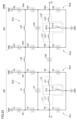
- FIG. 11 is an equivalent circuit diagram of a filter device according to a second modified example.
- 10A and 10B are a plan view and a side perspective view showing an example of the structure of the filter device of FIG. 9 .
- FIG. 11 is an equivalent circuit diagram of a filter device according to a third modified example.
- FIG. 12 is an exploded perspective view showing an example of a laminated structure of the filter device of FIG. 11 .
- FIG. 13 is an equivalent circuit diagram of a filter device according to a fourth modified example.
- FIG. 13 is an equivalent circuit diagram of a filter device according to a fifth modified example.
- FIG. 23 is an equivalent circuit diagram of a first example of a filter device according to Modification 6.
- FIG. 23 is an equivalent circuit diagram of a second example of the filter device of the sixth modified example.
- FIG. 11 is an equivalent circuit diagram of a filter device according to a second embodiment.
- FIG. 23 is an equivalent circuit diagram of a filter device according to a seventh modified example.
- FIG. 23 is an equivalent circuit diagram of a filter device according to Modification 8.
- FIG. 11 is an equivalent circuit diagram of a filter device according to a third embodiment.
- FIG. 21 is an exploded perspective view showing a first example of a laminated structure of the filter device of FIG. 20.
- FIG. 21 is an exploded perspective view showing a second example of the laminated structure of the filter device of FIG. 20.
- FIG. 13 is an equivalent circuit diagram of a filter device according to a ninth modified example.
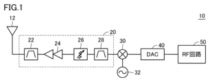
- FIG. 1 is a block diagram of a communication device 10 having a high-frequency front-end circuit 20 to which a filter device 100 according to embodiment 1 is applied.
- the communication device 10 is, for example, a mobile terminal such as a smartphone, or a mobile phone base station.
- the communication device 10 includes an antenna 12, a high-frequency front-end circuit 20, a mixer 30, a local oscillator 32, a digital-to-analog converter (DAC) 40, and an RF circuit 50.
- the high-frequency front-end circuit 20 also includes band-pass filters 22 and 28, an amplifier 24, and an attenuator 26. Note that, although FIG. 1 illustrates a case in which the high-frequency front-end circuit 20 includes a transmission circuit that transmits a high-frequency signal from the antenna 12, the high-frequency front-end circuit 20 may also include a reception circuit that receives a high-frequency signal via the antenna 12.
- the communication device 10 upconverts the transmission signal transmitted from the RF circuit 50 to a high-frequency signal and radiates it from the antenna 12.
- the modulated digital signal which is the transmission signal output from the RF circuit 50, is converted to an analog signal by the D/A converter 40.
- the mixer 30 mixes the transmission signal converted from a digital signal to an analog signal by the D/A converter 40 with an oscillation signal from the local oscillator 32 and upconverts it to a high-frequency signal.
- the bandpass filter 28 removes unnecessary waves generated by the upconversion and extracts only the transmission signal in the desired frequency band.
- the attenuator 26 adjusts the intensity of the transmission signal.
- the amplifier 24 power-amplifies the transmission signal that has passed through the attenuator 26 to a specified level.
- the bandpass filter 22 removes unnecessary waves generated during the amplification process and passes only signal components in the frequency band defined by the communication standard.
- the transmission signal that has passed through the bandpass filter 22 is radiated from the antenna 12.
- a filter device according to the present disclosure can be used as the bandpass filters 22, 28 in the communication device 10 described above.
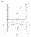
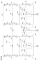
- Fig. 2 is an equivalent circuit diagram of the filter device 100.
- the filter device 100 includes an input terminal T1, an output terminal T2, a ground terminal GND, resonators RC1 to RC3, and a capacitor C5.
- Each of the resonators RC1 to RC3 is an LC resonator including an inductor and a capacitor.
- the resonator RC1 is an LC parallel resonator including a capacitor C1 and an inductor L1 connected in parallel between the input terminal T1 and the ground terminal GND.
- the inductor L1 includes inductors L11 and L12 connected in series between the input terminal T1 and the ground terminal GND.
- the inductor L11 is connected to the input terminal T1, and the inductor L12 is connected between the inductor L11 and the ground terminal GND.
- the resonator RC3 is an LC parallel resonator including a capacitor C2 and an inductor L2 connected in parallel between the output terminal T2 and the ground terminal GND.
- the inductor L2 includes inductors L21 and L12 connected in series between the input terminal T1 and the ground terminal GND.
- the inductor L21 is connected to the output terminal T2, and the inductor L12 is connected between the inductor L21 and the ground terminal GND.
- inductors L11 and L21 are connected in series between the input terminal T1 and the output terminal T2, and inductor L12 is connected between the connection node N12 of inductors L11 and L21 and the ground terminal GND. That is, inductor L12 is shared by resonators RC1 and RC3. With this configuration of inductors L1 and L2, resonators RC1 and RC3 are magnetically coupled.
- a capacitor C5 is connected between a connection node N1 of the capacitor C1 and the inductor L1 in the resonator RC1 and a connection node N2 of the capacitor C2 and the inductor L2 in the resonator RC3.
- the resonators RC1 and RC3 are electrically coupled by this capacitor C5.
- the resonator RC2 includes an inductor L3 and capacitors C3 and C4 connected to both ends of the inductor L3.
- the capacitor C3 is connected between one end of the inductor L3 and the connection node N1.
- the capacitor C4 is connected between the other end of the inductor L3 and the connection node N2.
- a capacitor C7 is connected between the connection node N3 of the inductor L3 and the capacitor C3 and the ground terminal GND
- a capacitor C8 is connected between the connection node N4 of the inductor L3 and the capacitor C4 and the ground terminal GND.
- Resonator RC2 is configured as a so-called open-ended LC resonator by inductor L3 and capacitors C3 and C4. Note that the configuration including capacitors C7 and C8 in addition to inductor L3 and capacitors C3 and C4 can also be considered as configuring an open-ended LC resonator.
- resonators RC1 and RC2 are connected by capacitor C3, and resonators RC2 and RC3 are connected by capacitor C4.
- resonators RC1 and RC2 are electrically coupled
- resonators RC2 and RC3 are electrically coupled.
- the filter device 100 there are two paths from the input terminal T1 to the output terminal T2: a first path that goes from resonator RC1 to resonator RC3 via resonator RC2, and a second path that goes directly from resonator RC1 to resonator RC3, skipping resonator RC2.
- An attenuation pole can be generated by the so-called "jump coupling" such as the second path.
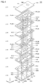
- Fig. 3 is an external perspective view of the filter device 100
- Fig. 4 is an exploded perspective view showing an example of the layered structure of the filter device 100.
- the filter device 100 includes a rectangular or approximately rectangular laminate 110 in which a plurality of dielectric layers LY1 to LY9 are laminated in the lamination direction.
- the dielectric layers LY1 to LY9 are formed of ceramics, such as low temperature co-fired ceramics (LTCC), or resin.
- LTCC low temperature co-fired ceramics
- the inductors and capacitors of the LC resonator are formed by a plurality of electrodes provided on each dielectric layer and a plurality of vias provided between the dielectric layers.
- the term "via” refers to a conductor provided in a dielectric layer to connect electrodes provided on different dielectric layers.
- the vias are formed, for example, by conductive paste, plating, and/or metal pins.
- the stacking direction of the dielectric layers LY1 to LY9 in the laminate 110 is referred to as the "Z-axis direction", the direction perpendicular to the Z-axis direction and along the first side of the laminate layer is referred to as the "X-axis direction”, and the direction along the second side of the laminate layer is referred to as the "Y-axis direction”.
- the positive direction of the Z-axis in each figure may be referred to as the upper side, and the negative direction as the lower side.
- the long side of the rectangular dielectric layer is referred to as the first side
- the short side is referred to as the second side.
- a directional mark DM for identifying the direction of the filter device 100 is arranged on the upper surface 111 (dielectric layer LY1: first surface) of the laminate 110.
- External terminals (input terminal T1, output terminal T2, and multiple ground terminals GND) for connecting the filter device 100 to external devices are arranged on the lower surface 112 (dielectric layer LY9: second surface) of the laminate 110.
- Each of the input terminal T1, output terminal T2, and ground terminals GND is a flat electrode, and is an LGA (Land Grid Array) terminal regularly arranged on the lower surface 112 of the laminate 110.
- the filter device 100 has three resonators RC1 to RC3, which are LC resonators. More specifically, resonator RC1 includes vias V10 to V12, VG13, a capacitor electrode PC10, and plate electrodes PL1A, PL1B, PL13A, and PL13B.
- Resonator RC2 includes vias V21 and V22, capacitor electrodes PC12, PC21, PC22, and PC23, and plate electrodes PL2A and PL2B.
- Resonator RC3 includes vias V30 to V32, VG13, a capacitor electrode PC30, and plate electrodes PL13A and PL13B. Note that via VG13 and plate electrodes PL13A and PL13B are shared by resonators RC1 and RC3.
- the input terminal T1 arranged on the lower surface 112 (dielectric layer LY9) of the laminate 110 is connected to the capacitor electrode PC10 arranged on the dielectric layer LY7 by a via V10.
- the capacitor electrode PC10 has a substantially rectangular shape, and when the laminate 110 is viewed in a plane from the stacking direction (Z-axis direction), at least a part of it overlaps with the ground electrode PG1 arranged on the dielectric layer LY8.
- the ground electrode PG1 is connected to the ground terminal GND arranged on the lower surface 112 by a plurality of vias VG1. That is, the capacitor electrode PC10 and the ground electrode PG1 form the capacitor C1 in FIG. 2.
- the capacitor electrode PC10 is connected to the flat plate electrode PL1A arranged on the dielectric layer LY4 and the flat plate electrode PL1B arranged on the dielectric layer LY5 by a via V11.
- the plate electrodes PL1A, PL1B are band-shaped electrodes formed with a roughly O-shaped wiring pattern, and have roughly the same shape when the laminate 110 is viewed in a plane from the stacking direction.
- a via V11 is connected to one end of each of the plate electrodes PL1A, PL1B, and a via V12 is connected to the other end.
- the via V12 is connected to the plate electrode PL13A arranged on the dielectric layer LY2 and the plate electrode PL13B arranged on the dielectric layer LY3.
- the plate electrodes PL13A and PL13B are strip-shaped electrodes formed by combining C-shaped wiring patterns, and have approximately the same shape when the laminate 110 is viewed in a plane from the stacking direction.
- each of the plate electrodes PL13A and PL13B has a shape that is linearly symmetrical with respect to a virtual line CL that passes through the center of the X-axis and is parallel to the Y-axis.
- a via V12 is connected to one end of each of the plate electrodes PL13A and PL13B, and a via V32 is connected to the other end.
- a via VG13 is connected to the center of each of the paths of the plate electrodes PL13A and PL13B.
- the via VG13 is connected to a ground electrode PG1 arranged on the dielectric layer LY8.
- the inductor L11 in FIG. 2 is formed by the vias V10 to V12, the plate electrodes PL1A and PL1B, and the path from the connection point of the via V12 to the connection point of the via VG13 on the plate electrodes PL13A and PL13B. Also, the inductor L12 in FIG. 2 is formed by the via VG13.
- the output terminal T2 arranged on the lower surface 112 of the laminate 110 is connected to the capacitor electrode PC30 arranged on the dielectric layer LY7 by a via V30.
- the capacitor electrode PC30 has a substantially rectangular shape and is arranged adjacent to the capacitor electrode PC10.
- the capacitor electrode PC30 at least partially overlaps with the ground electrode PG1 arranged on the dielectric layer LY8. That is, the capacitor electrode PC30 and the ground electrode PG1 form the capacitor C2 in FIG. 2.
- the capacitor electrode PC30 is connected to the plate electrode PL3A arranged on the dielectric layer LY4 and the plate electrode PL3B arranged on the dielectric layer LY5 by a via V31.
- the plate electrodes PL3A, PL3B are band-shaped electrodes formed with a wiring pattern that is roughly O-shaped, and have roughly the same shape when the laminate 110 is viewed in a plane from the stacking direction.
- the plate electrodes PL3A, PL3B have a shape that is linearly symmetrical to the plate electrodes PL1A, PL1B.
- a via V31 is connected to one end of each of the plate electrodes PL3A, PL3B, and a via V32 is connected to the other end.
- the via V32 is connected to the plate electrode PL13A arranged on the dielectric layer LY2 and the plate electrode PL13B arranged on the dielectric layer LY3.
- the inductor L21 in FIG. 2 is formed by the vias V30 to V32, the plate electrodes PL3A and PL3B, and the path from the connection point of the via V32 to the connection point of the via VG13 on the plate electrodes PL13A and PL13B. Also, as described above, the inductor L12 in FIG. 2 is formed by the via VG13.
- each of the capacitor electrode PC10 of the resonator RC1 and the capacitor electrode PC20 of the resonator RC2 partially overlaps with the linear capacitor electrode PC13 arranged on the dielectric layer LY6.
- the capacitor electrodes PC10, PC13, and PC30 form the capacitor C5 in FIG. 2.
- capacitor electrodes PC21 and PC22 are arranged adjacent to capacitor electrodes PC10 and PC30 in the positive direction of the Y axis.
- Each of the capacitor electrodes PC21 and PC22 has the same shape, which is a substantially rectangular shape.
- each of the capacitor electrodes PC21 and PC22 at least partially overlaps with the ground electrode PG1 arranged on the dielectric layer LY8. That is, the capacitor electrode PC21 and the ground electrode PG1 form the capacitor C7 in FIG. 2.
- the capacitor electrode PC22 and the ground electrode PG1 form the capacitor C8 in FIG. 2.
- the capacitor electrode PC21 When the laminate 110 is viewed in a plan view from the stacking direction, the capacitor electrode PC21 partially overlaps with the capacitor electrode PC12 disposed on the dielectric layer LY6.
- the capacitor electrode PC12 has a substantially rectangular shape and is connected to the capacitor electrode PC10 of the resonator RC1 by a via V13. In other words, the capacitor electrode PC21 and the capacitor electrode PC12 form the capacitor C3 in FIG. 1.
- the capacitor electrode PC22 partially overlaps with the capacitor electrode PC23 disposed on the dielectric layer LY6.
- the capacitor electrode PC23 has a substantially rectangular shape, and is connected to the capacitor electrode PC30 of the resonator RC3 by a via V23. That is, the capacitor electrode PC22 and the capacitor electrode PC23 form the capacitor C4 in FIG. 1.
- the capacitor electrode PC21 is connected by a via V21 to a plate electrode PL2A arranged on the dielectric layer LY2 and a plate electrode PL2B arranged on the dielectric layer LY3.
- the plate electrodes PL2A, PL2B are band-shaped electrodes formed in a substantially C-shaped wiring pattern and have substantially the same shape.
- the plate electrodes PL2A, PL2B have a shape that is line-symmetrical with respect to the imaginary line CL.
- each of the plate electrodes PL2A and PL2B extends along the plate electrodes PL13A and PL13B included in the resonators RC1 and RC2. This arrangement magnetically couples the plate electrodes PL2A and PL13A, and the plate electrodes PL2B and PL13B.
- a via V12 is connected to one end of each of the plate electrodes PL2A and PL2B, and a via V22 is disposed at the other end.
- the via V22 is connected to a capacitor electrode PC22 disposed on the dielectric layer LY7.
- the vias V21 and V22 and the plate electrodes PL2A and PL2B constitute the inductor L3 in FIG. 2.
- the elements in the laminate 110 that constitutes the filter device 100 are arranged as a whole so as to be linearly symmetrical with respect to the imaginary line CL.
- Attenuation poles In a bandpass filter, it is necessary to place attenuation poles on both the higher and lower frequency sides of the desired frequency band to be passed.
- One method of generating attenuation poles in a filter device composed of multiple resonators is known to be by forming a "jump coupling" that bypasses the series path of the resonators from the input terminal to the output terminal.
- the number of attenuation poles generated by "jump coupling” is determined by the difference in the number of resonators between the main path, in which the signal to be transmitted passes through all resonators, and the sub-path, in which the signal is transmitted by skipping some of the resonators. Therefore, in principle, to generate two attenuation poles by jump coupling, it is necessary to arrange four or more stages of resonators.
- Such bandpass filters may be used in small communication devices such as mobile phones and smartphones. In such devices, there is still a high demand for further miniaturization and low height, and therefore further miniaturization of the bandpass filter itself is required.
- a bandpass filter composed of multiple resonators the number of elements (plate electrodes, vias) that constitute the inductor and capacitor of each resonator greatly affects the size of the device. Therefore, reducing the number of resonators included in the filter can be one way to realize a miniaturized bandpass filter.
- resonators are used for the resonators included in the bandpass filter, and by devising the manner of coupling between the resonators, even a filter composed of three resonators is configured to function as a bandpass filter by arranging attenuation poles on both sides of the passband.
- the first-stage resonator connected to the input terminal and the second-stage resonator connected to the output terminal are magnetically coupled and electrically coupled. Furthermore, by adopting a resonator with both ends open for the second-stage resonator, the coupling between the first-stage resonator and the second-stage resonator and the coupling between the second-stage resonator and the third-stage resonator are made different in coupling mode in the frequency band to be passed.
- the degree of coupling of the sub-path between the input terminal and the third-stage resonator, or between the first-stage resonator and the output terminal can be relatively strengthened compared to the degree of coupling of the sub-path between the first-stage resonator and the third-stage resonator.
- points are generated on both sides of the desired passband where the signal passing through the main path and the signal passing through the sub-path have the same amplitude and opposite phase, and attenuation poles can be generated at these points. Therefore, even in a three-stage filter device, attenuation poles can be arranged on both sides of the passband to function as a bandpass filter.
- FIG. 5 is a diagram for explaining the topology showing the coupling state between resonators in the filter device 100 of the first embodiment and the comparative four-stage filter device 100X.
- the left diagram shows the topology corresponding to the filter device 100 of the first embodiment
- the right diagram shows the topology corresponding to the comparative filter device 100X.
- the "IN” and "OUT" nodes correspond to the input terminal and output terminal, respectively, and the nodes indicated by numbers correspond to each resonator.
- “+” indicates electric field coupling
- "-" indicates magnetic coupling.
- the coupling between the resonators is electric field coupling.
- the difference in the number of resonators passed through between the main path that goes from the first resonator to the fourth resonator via the second and third resonators, and the sub-path that directly couples from the first resonator to the fourth resonator is two. This makes it possible to generate two or more attenuation poles in a symmetrical structure.
- a cross coupling is formed between the first and third stage resonators.
- a double-open resonator in which capacitors are placed on both ends of an inductor is used as the second stage resonator.
- the electric field generated in a double-open resonator becomes zero near the center of the resonator, one end has positive polarity (+) and the other end has negative polarity (-). This results in a different coupling mode between the first and second stage resonators and the second and third stage resonators.
- the degree of cross-coupling between the first-stage and third-stage resonators is partially offset by the electric-field coupling and magnetic coupling, and becomes weaker.
- the degree of coupling between the input terminal and the third-stage resonator, or the degree of coupling between the first-stage resonator and the output terminal becomes relatively stronger than the degree of coupling between the first-stage and third-stage resonators.
- the filter device can function as a bandpass filter.
- the second stage resonator In order to invert the polarity of the coupling in the signal path, for example, it is possible to configure the second stage resonator as a one-side grounded type resonator similar to the first and third stages, and to use magnetic coupling between the first and second stage resonators using an inductor, and electric field coupling between the second and third stage resonators using a capacitor. In this case, however, the element arrangement of the entire filter device becomes asymmetric. In the case of asymmetric element arrangement, variations in characteristics are likely to occur due to placement errors in the manufacturing process, and the standard values (Typ values) of the characteristics are also likely to deteriorate.
- the filter device of embodiment 1 by using a resonator with both ends open for the second-stage resonator, it is possible to invert the polarity of the coupling between the first-stage and second-stage resonators and the polarity of the coupling between the second-stage and third-stage resonators in the main signal transmission path (main path) even if the element arrangement of the entire filter device is symmetrical.
- FIG. 6 and 7 are diagrams for explaining the filter characteristics of the filter device 100 of the first embodiment and the filter device 100X of the comparative example.
- the horizontal axis indicates frequency
- the vertical axis indicates the insertion loss and return loss of each filter device.
- Fig. 7 is an enlarged view of the insertion loss near the passband of Fig. 6.
- solid lines LN10 and LN15 indicate the insertion loss and return loss, respectively, of the filter device 100 of the first embodiment
- dashed lines LN11 and LN16 indicate the insertion loss and return loss, respectively, of the filter device 100X of the comparative example.
- the filter device 100 of the first embodiment also has attenuation poles on both sides of the pass band, and can function as a bandpass filter.
- the attenuation pole on the lower frequency side of the pass band is farther away from the pass band than in the case of the comparative filter device 100X of a four-stage configuration (dashed line LN11) due to the reduced number of resonators, and the steepness of the attenuation characteristics near the pass band is slightly worse.
- the filter device 100 of the first embodiment has improved insertion loss, especially on the lower frequency side, due to the reduced number of resonators, compared to the comparative filter device 100X.
- the filter device 100 of the first embodiment which is a filter device composed of three resonators
- a resonator with both ends open is used as the second-stage resonator
- the first-stage resonator and the third-stage resonator are cross-coupled using magnetic coupling and electric field coupling, so that the filter device can function as a bandpass filter.
- the elements in the laminate can be arranged symmetrically, it is possible to suppress variation in characteristics.
- connection node N1 and “connection node N2" in the first embodiment correspond to the “first terminal” and “second terminal” in this disclosure, respectively.
- the "resonator RC1", “resonator RC2”, and “resonator RC3” in the first embodiment correspond to the “first resonator”, “second resonator”, and “third resonator” in this disclosure, respectively.
- the “capacitors C1” to C5", “capacitor C7”, and “capacitor C8” in the first embodiment correspond to the “first capacitor” to "fifth capacitor”, “seventh capacitor”, and “eighth capacitor” in this disclosure, respectively.
- the “inductors L1” to “inductors L3” in the first embodiment correspond to the "first inductor” to “third inductor” in this disclosure, respectively.
- Capacitor electrode PC10 corresponds to the "first capacitor electrode” to the "seventh capacitor electrode” in this disclosure, respectively.
- Platinum electrodes PL13A, PL13B” in embodiment 1 correspond to the “first plate electrode” and the “second plate electrode” in this disclosure.
- Platinum electrodes PL2A, PL2B” in embodiment 1 correspond to the “third plate electrode” in this disclosure.
- Volia VG13, “via V21”, and “via V22” in embodiment 1 correspond to the "first via” to the "third via” in this disclosure, respectively.
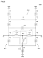
- FIG. 8 is an exploded perspective view showing an example of the laminated structure of the filter device 100A of the first modified example.
- the laminate 110 of the filter device 100A includes dielectric layers LY11 to LY16 laminated in the lamination direction (Z-axis direction).
- a directional mark DM for identifying the orientation of the filter device 100A is arranged on the upper surface 111 (dielectric layer LY11: first surface) of the laminate 110.
- An input terminal T1, an output terminal T2, and a ground terminal GND for connecting the filter device 100A to an external device are arranged on the lower surface 112 (dielectric layer LY16: second surface) of the laminate 110.
- the ground terminal GND is a roughly H-shaped flat electrode with a notch formed in one portion.
- the input terminal T1 is arranged in the notch formed in the negative direction of the X-axis of the dielectric layer LY16.
- the input terminal T1 is arranged in the notch formed in the positive direction of the X-axis of the dielectric layer LY16.
- a ground electrode PG2 is disposed on the dielectric layer LY12 so as to cover the entire surface of the dielectric layer.
- the ground electrode PG2 is connected to the ground terminal GND of the dielectric layer LY16 by a number of vias VG2 disposed around the laminate 110 along the side of the laminate 110.
- the input terminal T1 arranged on the lower surface 112 of the laminate 110 is connected by a via V1 to a plate electrode PL50 arranged on the dielectric layer LY14.
- the plate electrode PL50 has a shape in which one end of each of two L-shaped wiring patterns (first electrode, second electrode) is connected to a wiring pattern (third electrode) of approximately rectangular shape extending in the X-axis direction.
- the two L-shaped wiring patterns are arranged so as to be linearly symmetrical with respect to a virtual line CL that passes through the center of the X-axis of the dielectric layer and is parallel to the Y-axis.
- the via V1 connected to the input terminal T1 is connected to the wiring pattern (first electrode) arranged in the negative direction of the X-axis among the L-shaped wiring patterns.
- the output terminal T2 is arranged through a via V2 on the L-shaped wiring pattern (second electrode) arranged in the positive direction of the X-axis.
- the third electrode connecting the two L-shaped wiring patterns is connected to the ground electrode PG2 and the ground terminal GND by a via VG2.
- the plate electrode PL50 overlaps with the ground electrode PG2 and the ground terminal GND.
- the via V1 and the first and third electrodes of the plate electrode PL50 form the inductor L1 in the resonator RC1 of the equivalent circuit in FIG. 2, and furthermore, the capacitance component generated between this portion and the ground electrode PG2 and the ground terminal GND forms the capacitor C1 in FIG. 2.
- the via V2 and the second and third electrodes of the plate electrode PL50 form the inductor L2 and capacitor C2, respectively, in the resonator RC3 in FIG. 2.
- the plate electrode PL51 is disposed adjacent to the plate electrode PL50 along the portions of the first and second electrodes of the plate electrode PL50 that extend along the X-axis.
- the inductance component of the plate electrode PL51 constitutes the inductor L3 in FIG. 2.
- the capacitance components generated between the plate electrode PL51 and the ground electrode PG2 and between the plate electrode PL51 and the ground terminal GND constitute the capacitors C7 and C8 in FIG. 2.
- Capacitor electrodes PC51, PC52, and PC53 are disposed on the dielectric layer LY13.
- the capacitor electrode PC51 partially overlaps both the first electrode of the plate electrode PL50 and the plate electrode PL51.
- the plate electrodes PL50, PL51, and the capacitor electrode PC51 form the capacitor C3 in FIG. 2.
- the capacitor electrode PC52 partially overlaps both the second electrode of the plate electrode PL50 and the plate electrode PL51.
- the plate electrodes PL50, PL51, and the capacitor electrode PC52 form the capacitor C4 in FIG. 2. That is, the plate electrode PL51 and the capacitor electrodes PC51, PC52 form the resonator RC2 in FIG. 2.
- the capacitor electrode PC53 partially overlaps both the first electrode and the second electrode of the plate electrode PL50.
- the first electrode and the second electrode of the plate electrode PL50 and the capacitor electrode PC53 form the capacitor C5 in FIG. 2.
- the plate electrode PL51 is arranged so as to be line-symmetrical with respect to the imaginary line CL. Furthermore, the capacitor electrodes PC51 and PC52 are arranged so as to be line-symmetrical with respect to the imaginary line CL. That is, in the filter device 100A, the elements arranged in the laminate 110 are arranged symmetrically as a whole with respect to the imaginary line CL.
- the equivalent circuit shown in FIG. 2 can be realized with the configuration of the filter device 100A shown in FIG. 8. Therefore, the filter device 100A can achieve the same effects as the filter device 100 of the first embodiment.
- the "plate electrode PL51,” “capacitor electrode PC51,” “capacitor electrode PC51,” and “ground electrode PG2" in Modification 1 correspond to the "fourth electrode” to “seventh electrode” in this disclosure, respectively.
- FIG. 9 is an equivalent circuit diagram of filter device 100B of modified example 2.
- Filter device 100B has a configuration in which a capacitor C6 is added to the equivalent circuit diagram of filter device 100 shown in FIG. 2.
- the configuration other than capacitor C6 is the same as in FIG. 2, and the description of the elements that overlap with FIG. 2 will not be repeated.
- the capacitor C6 is connected between the connection node N13 between the capacitor C1 of the resonator RC1, the capacitor C2 of the resonator RC3, and the inductor L12 shared by the resonators RC1 and RC3, and the ground terminal GND.
- FIG. 10 is a plan view (top (A)) and a side view (bottom (B)) showing an example of the structure of the filter device 100B of FIG. 9.
- the filter device 100B is a resonator in which each resonator is composed only of a plate electrode without using vias.
- the filter device 100B includes an input terminal T1, an output terminal T2, a ground terminal GND, plate electrodes PL60, PL65, capacitor electrodes PC12A, PC23A, ground electrodes PG10, PG20, PG30, and vias V60, V61.
- the filter device 100B has a laminate 110 in which multiple dielectric layers are stacked.
- a ground terminal GND is disposed over the side surface and part of the bottom surface 112 of the laminate 110.
- ground electrodes PG10, PG20 are disposed over the entire surface of the dielectric layers adjacent to the top surface 111 and bottom surface 112 of the laminate 110.
- the ground electrodes PG10, PG20 are connected to the ground terminal GND at the side surface.
- the plate electrode PL60 constituting the resonators RC1 and RC3 and the plate electrode PL65 constituting the resonator RC2 are arranged on the same dielectric layer between the ground electrodes PG10 and PG20.
- the plate electrode PL60 includes a first electrode PL61 connected through a via V60 to an input terminal T1 arranged on the lower surface 112, a second electrode PL62 connected through a via V61 to an output terminal T2 arranged on the lower surface 112, and a third electrode PL63 connected to the first electrode PL61 and the second electrode PL62.
- the first electrode PL61 and the second electrode PL62 each have a roughly Y-shape with three ends, and are symmetrical to each other.
- a via V60 is connected to a first end of the first electrode PL61.
- a via V61 is connected to a first end of the second electrode PL62.
- the second ends of the first electrode PL61 and the second electrode PL62 are connected to each other.
- the third ends of the first electrode PL61 and the second electrode PL62 are opposed to each other, separated by a predetermined distance (region RG1).
- the opposed portions of region RG1 form the capacitor C5 in FIG. 9.
- the third electrode PL63 is a substantially rectangular electrode and is connected to the second ends of the first electrode PL61 and the second electrode PL62.
- the third electrode PL63 is not connected to the ground terminal GND on the side.
- Resonator RC1 is formed by the inductance components (corresponding to inductor L1 in FIG. 9) in the first electrode PL61 and the third electrode PL63, and the capacitance components (corresponding to capacitor C1 in FIG. 9) that arise between the portions and the ground electrodes PG10 and PG20.
- Resonator RC3 is formed by the inductance components (corresponding to inductor L2 in FIG. 9) in the second electrode PL62 and the third electrode PL63, and the capacitance components (corresponding to capacitor C2 in FIG. 9) that arise between the portions and the ground electrodes PG10 and PG20.
- the ground electrode PG30 is a flat electrode of a generally rectangular shape extending in the X-axis direction, and is connected to the ground terminal GND on the side closest to the third electrode PL63.
- the ground electrode PG30 is disposed on a dielectric layer different from the third electrode PL63, and at least a portion of the ground electrode PG30 overlaps with the third electrode PL63 when the laminate 110 is viewed in a plane from the stacking direction (Z-axis direction).
- the third electrode PL63 and the ground electrode PG30 form the capacitor C6 in FIG. 9.
- the plate electrode PL65 is an electrode having a substantially rectangular shape that is disposed close to the first electrode PL61 and the second electrode PL62 along the second ends extending in the X-axis direction.
- the capacitance components of the plate electrode PL65 and the ground electrodes PG10 and PG20 form the capacitors C7 and C8 in FIG. 9.
- Each of the capacitor electrodes PC12A, PC23A is an electrode having a substantially rectangular shape and arranged on a dielectric layer different from the plate electrodes PL60, PL65.
- the capacitor electrode PC12A partially overlaps the first electrode PL61 and the plate electrode PL65.
- the first electrode PL61, the plate electrode PL65, and the capacitor electrode PC12A form the capacitor C3 in FIG. 9.
- the capacitor electrode PC23A partially overlaps the second electrode PL62 and the plate electrode PL65. That is, the second electrode PL62, the plate electrode PL65, and the capacitor electrode PC23A form the capacitor C4 in FIG. 9.
- the resonant frequency of the resonators RC1 and RC3 can change depending on the dimension of the plate electrode PL60 in the Y-axis direction. If the third electrode PL63 of the plate electrode PL60 is connected to the ground terminal GND, for example, if a cutting error occurs during dicing of the device or the dielectric layer is misaligned, the dimension of the third electrode PL63 in the Y-axis direction will fluctuate, significantly affecting the filter characteristics.
- the "plate electrode PL65,” “capacitor electrode PC12A,” “capacitor electrode PC23A,” and “ground electrode PG30" in the modified example correspond to the "fourth electrode” to “seventh electrode” in this disclosure, respectively.
- FIG. 11 is an equivalent circuit diagram of filter device 100C of modified example 3.
- Filter device 100C has a configuration in which capacitors C9 and C10 are added to filter device 100 of embodiment 1 shown in FIG. 2.
- FIG. 11 the description of elements that overlap with FIG. 2 will not be repeated.
- a capacitor C9 is connected between the connection node N1 of the resonator RC1 and the input terminal T1
- a capacitor C10 is connected between the connection node N2 of the resonator RC3 and the output terminal T2.
- the capacitors C9 and C10 make it possible to adjust the impedance matching between the filter device and external equipment within the passband.
- FIG. 12 is an exploded perspective view showing an example of the layered structure of filter device 100C of FIG. 11.
- Filter device 100C differs from filter device 100A of modified example 1 shown in FIG. 8 in the configuration of the connection portion between input terminal T1 and output terminal T2 and plate electrode PL50.
- the other configuration is the same as in FIG. 8, and the description of the elements that overlap with FIG. 8 will not be repeated.
- the input terminal T1 is connected by a via V1A to a capacitor electrode PC1A disposed on the dielectric layer LY15.
- a capacitor electrode PC1A disposed on the dielectric layer LY15.
- the laminate 110 is viewed in a plan view from the stacking direction, at least a portion of the capacitor electrode PC1A overlaps with the plate electrode PL50.
- the capacitor electrode PC1A and the plate electrode PL50 form the capacitor C9 in FIG. 11.
- the output terminal T2 is connected by a via V2A to a capacitor electrode PC2A disposed on the dielectric layer LY15.
- a capacitor electrode PC2A disposed on the dielectric layer LY15.
- This configuration makes it possible to realize the circuit shown in Figure 11, and suppresses the deterioration of attenuation characteristics caused by DC components.
- Capacitor C9 and “Capacitor C10” in Modification 3 correspond to the “ninth capacitor” and “tenth capacitor” in this disclosure, respectively.
- FIG. 13 is an equivalent circuit diagram of a filter device 100D of the fourth modified example.
- the capacitors C6 and C7 in the filter device 100 shown in FIG. 2 are deleted.
- the resonator RC2 formed by the inductor L3 and the capacitors C3 and C4 is a resonator with both ends open, so that the same effect as the filter device 100 of the first embodiment can be achieved.
- FIG. 14 is an equivalent circuit diagram of a filter device 100E1 of modified example 5.
- a capacitor C4 is disposed in the position of the capacitor C5 in the filter device 100D shown in FIG. 13.
- the connection node of the inductor L3 and the capacitor C4 is connected to the connection node N2 of the resonator RC3, and the connection node of the capacitor C3 and the capacitor C4 is connected to the connection node N1 of the resonator RC1.
- the resonator RC2 in the filter device 100D of FIG. 13 is replaced with an LC series resonator composed of the inductor L3 and the capacitor C3.
- Resonator RC2 is capacitively coupled to resonator RC1 and magnetically coupled to resonator RC3. Therefore, even in this configuration, resonators RC1 and RC3 are capacitively coupled to each other and magnetically coupled, and further, the polarity of the coupling between resonator RC2 and resonator RC1 is opposite to the polarity of the coupling between resonator RC2 and resonator RC3. Therefore, the configuration of filter device 100E1 can achieve the same effects as filter device 100 of embodiment 1.
- the configuration has been described in which the resonators RC1 and RC3 are capacitively coupled by the capacitor C4 of the resonator RC2.
- the resonators RC1 and RC3 may be capacitively coupled by the capacitor C3 of the resonator RC2.
- FIG. 16 is an equivalent circuit diagram of a filter device 100F of the sixth modified example.
- the inductor L1 included in the resonator RC1 and the inductor L2 included in the resonator RC3 are configured as independent individual inductors.
- the vias or wiring patterns that configure the inductors L1 and L2 are arranged close to each other inside the laminate 110 so that they are magnetically coupled to each other. In this way, even when the resonators RC1 and RC3 are configured as independent resonators, the same effects as those of the first embodiment can be achieved.
- the capacitor C5 that capacitively couples the resonators RC1 and RC3 is arranged separately, but for example, the capacitor electrode that constitutes the capacitor C1 of the resonator RC1 and the capacitor electrode that constitutes the capacitor C2 of the resonator RC3 may be arranged adjacent to each other, and the capacitor C5 may be formed by the parasitic capacitance between these capacitor electrodes.
- the coupling between the first and second resonators and the coupling between the second and third resonators are capacitive coupling.
- the coupling between the first and second resonators and the coupling between the second and third resonators are magnetic coupling.
- FIG. 17 is an equivalent circuit diagram of a filter device 100G of the second embodiment.
- the capacitors C7 and C8 in the filter device 100 of the first embodiment shown in FIG. 2 are deleted.
- the capacitors C3 and C4 are not connected to the resonators RC1 and RC3, but are connected to each other.
- the inductor L3 is magnetically coupled to the inductor L1 of the resonator RC1 and the inductor L2 of the resonator RC3. More specifically, in FIG. 17, the inductor L3 is represented as inductors L31 and L32 connected in series, with the inductor L31 portion magnetically coupled to the inductor L11 portion of the inductor L1, and the inductor L32 portion magnetically coupled to the inductor L21 portion of the inductor L2.
- the “inductor L31" and “inductor L32" in the second embodiment correspond to the "fourth inductor” and "fifth inductor” in this disclosure, respectively.
- FIG. 18 is an equivalent circuit diagram of a filter device 100H of modified example 7.
- one end of the capacitor C3 in the resonator RC2 is connected to the inductor L31 (connection node N3), and the other end is connected to the ground terminal GND.
- one end of the capacitor C4 in the resonator RC2 is connected to the inductor L32 (connection node N4), and the other end is connected to the ground terminal GND.
- the inductor L31 of the resonator RC2 is also magnetically coupled to the inductor L11 of the resonator RC1, and the inductor L32 of the resonator RC2 is magnetically coupled to the inductor L21 of the resonator RC3.
- resonator RC2 is configured as a resonator with both ends open, so that the same effects can be achieved as with filter device 100 of embodiment 1 and filter device 100G of embodiment 2.
- FIG. 19 is an equivalent circuit diagram of a filter device 100I of modified example 8.
- the connection node N3 between the inductor L3 and the capacitor C3 of the resonator RC2 in the configuration of the filter device 100G, and/or the connection node N4 between the inductor L3 and the capacitor C4, are connected to the ground terminal GND.
- resonator RC2 is configured as a resonator with both ends open, so that the same effects can be achieved as with filter device 100 of embodiment 1 and filter device 100G of embodiment 2.
- FIG. 20 is an equivalent circuit diagram of a filter device 300 according to the third embodiment.
- the filter device 300 includes two filter circuits 200 and 250, and a capacitor C40 and an inductor L40 for connecting the filter circuits.
- the inductor L40 includes inductors L41 to L43.
- Each of the filter circuits 200 and 250 basically has a configuration corresponding to the circuit of the filter device 100 of the first embodiment.
- the elements included in the filter circuit 200 are given the same reference symbols as the elements of the filter device 100 of the first embodiment.
- the resonators RC4 to RC6 in the filter circuit 250 correspond to the resonators RC1 to RC3 in the filter device 100, respectively.
- the capacitors C51 to C55, C57, and C58 in the filter circuit 250 correspond to the capacitors C1 to C5, C7, and C8 in the filter device 100, respectively.
- the inductors L51 to L53, L511, L512, and L521 in the filter circuit 250 correspond to the inductors L1 to L3, L11, L12, and L21 in the filter device 100, respectively.
- the connection nodes N1 to N4, and N12 in the filter circuit 250 correspond to the connection nodes N51 to N54, and N512 in the filter device 100, respectively.
- connection node N1 of the filter circuit 200 is connected to the input terminal T1.
- connection node N52 of the filter circuit 250 is connected to the output terminal T2.
- Inductors L41 and L42 are connected in series between the connection node N2 of the filter circuit 200 and the connection node N51 of the filter circuit 250.
- Inductor L43 is connected between the connection node N412 of the inductors L41 and L42 and the ground terminal GND.
- the resonator RC3 of the filter circuit 200 and the resonator RC4 of the filter circuit 250 are magnetically coupled.
- a capacitor C40 is connected between the connection node N4 of the filter circuit 200 and the connection node N53 of the filter circuit 250.
- the resonator RC2 of the filter circuit 200 and the resonator RC5 of the filter circuit 250 are electrically coupled.
- two attenuation poles can be generated on the higher and lower frequency sides of the passband in each of the three-stage filter circuits 200, 250, so that the filter device can function as a bandpass filter. Furthermore, since the signal to be passed passes through more resonators than in the configuration of embodiment 1, the amount of attenuation can be made greater than that of the filter device 100 of embodiment 1.
- each of the filter circuits 200 and 250 has a symmetrical structure, and the filter device 300 also has a symmetrical structure overall. This makes it possible to reduce the variation in characteristics due to placement errors in the manufacturing process.
- FIG. 21 is an exploded perspective view showing a first example of a laminated structure of the filter device 300 according to the third embodiment.
- the inductors and capacitors constituting the filter device 300 are formed by vias and wiring patterns.
- the laminate 110 of the filter device 300 includes dielectric layers LY21 to LY29 stacked in the stacking direction (Z-axis direction).
- a directional mark DM for identifying the orientation of the filter device 300 is arranged on the upper surface 111 (dielectric layer LY21: first surface) of the laminate 110.
- External terminals (input terminal T1, output terminal T2, and multiple ground terminals GND) for connecting the filter device 300 to external devices are arranged on the lower surface 112 (dielectric layer LY29: second surface) of the laminate 110.
- Each of the input terminal T1, output terminal T2, and ground terminals GND is a flat electrode, and is an LGA terminal regularly arranged on the lower surface 112 of the laminate 110.
- the input terminal T1 is connected to a capacitor electrode PC71 arranged on the dielectric layer LY27 by a via V71.
- the capacitor electrode PC71 is a flat electrode having a substantially rectangular shape extending in the Y-axis direction. At least a portion of the capacitor electrode PC71 overlaps with the ground electrode PG10 arranged on the dielectric layer LY28 when the laminate 110 is viewed in a plan view from the stacking direction.
- the ground electrode PG10 is disposed over almost the entire surface of the dielectric layer LY28, and is connected to the ground terminal GND disposed on the dielectric layer LY29 by a plurality of vias VG4.
- the capacitor electrode PC71 and the ground electrode PG10 form the capacitor C1 in FIG. 20.
- the via V71 passes through the ground electrode PG10.
- the capacitor electrode PC71 is further connected by a via V72 to a plate electrode PL71A arranged on the dielectric layer LY22 and a plate electrode PL71B arranged on the dielectric layer LY23.
- Each of the plate electrodes PL71A, PL71B is a band-shaped electrode having a roughly C-shape with an opening formed in the negative direction of the Y-axis when the laminate 110 is viewed in a plan view from the stacking direction.
- the plate electrodes PL71A and PL71B have the same shape.
- a via V72 is connected to one end of each of the plate electrodes PL71A and PL71B, and a via V73 is connected to the other end.
- the via V73 is connected to a capacitor electrode PC73 arranged on the dielectric layer LY27.
- the capacitor electrode PC73 has the same shape as the capacitor electrode PC71 and is arranged in the positive direction of the X-axis relative to the capacitor electrode PC71. At least a portion of the capacitor electrode PC73 overlaps with the ground electrode PG10 of the dielectric layer LY28 when the laminate 110 is viewed in a plane from the stacking direction.
- the capacitor electrode PC73 and the ground electrode PG10 form the capacitor C2 in FIG. 20.
- a via VG71 is connected to the center position along the path from one end of the plate electrodes PL71A, PL71B to the other end.
- the via VG71 is connected to the ground electrode PG10 of the dielectric layer LY28.
- the vias V72, VG71 and the plate electrodes PL71A, PL71B form the inductor L1 in FIG. 20.
- the vias V73, VG71 and the plate electrodes PL71A, PL71B form the inductor L2 in FIG. 20.
- a capacitor electrode PC721 is arranged in the positive direction of the Y axis relative to the capacitor electrode PC71 and spaced apart from the capacitor electrode PC71. Furthermore, a capacitor electrode PC722 is arranged in the positive direction of the Y axis relative to the capacitor electrode PC73 and spaced apart from the capacitor electrode PC73.
- the capacitor electrodes PC721 and PC722 are flat electrodes of the same shape having a substantially rectangular shape, and at least a portion of them overlap with the ground electrode PG10 of the dielectric layer LY28 when the laminate 110 is viewed in a plane from the stacking direction.
- the capacitor electrodes PC721 and PC722 and the ground electrode PG10 respectively constitute the capacitors C7 and C8 in FIG. 20.
- the capacitor electrode PC721 is connected by a via V741 to a plate electrode PL72A arranged on the dielectric layer LY22 and a plate electrode PL72B arranged on the dielectric layer LY23.
- Each of the plate electrodes PL72A, PL72B is a band-shaped electrode having a roughly C-shape with an opening formed in the positive direction of the Y-axis when the laminate 110 is viewed in a plan view from the stacking direction.
- the plate electrodes PL72A and PL72B have the same shape.
- a via V741 is connected to one end of the plate electrodes PL72A and PL72B, and a via V742 is connected to the other end.
- the via V742 is connected to the capacitor electrode PC722 of the dielectric layer LY27.
- Capacitor electrodes PC81, PC82, and PC83 are arranged on the dielectric layer LY26.
- Capacitor electrode PC81 partially overlaps with capacitor electrodes PC71 and PC721 when the laminate 110 is viewed in a plan view from the stacking direction.
- Capacitor electrodes PC71, PC721, and PC81 form capacitor C3 in FIG. 20.
- the capacitor electrode PC82 When the laminate 110 is viewed in a plan view from the stacking direction, the capacitor electrode PC82 partially overlaps with the capacitor electrodes PC73 and PC722. The capacitor electrodes PC73, PC722, and PC82 form the capacitor C4 in FIG. 20.
- the capacitor electrode PC83 When the laminate 110 is viewed in a plan view from the stacking direction, the capacitor electrode PC83 partially overlaps with the capacitor electrodes PC71 and PC73.
- the capacitor electrodes PC71, PC73, and PC83 form the capacitor C5 in FIG. 20.
- the output terminal T2 is connected to a capacitor electrode PC76 arranged on the dielectric layer LY27 by a via V78.
- the capacitor electrode PC76 is a flat electrode having a substantially rectangular shape extending in the Y-axis direction. At least a portion of the capacitor electrode PC76 overlaps with the ground electrode PG10 of the dielectric layer LY28 when the laminate 110 is viewed in a plane from the stacking direction.
- the capacitor electrode PC76 and the ground electrode PG10 form the capacitor C52 in FIG. 20.
- the capacitor electrode PC78 is further connected by a via V76 to a plate electrode PL75A arranged on the dielectric layer LY22 and a plate electrode PL75B arranged on the dielectric layer LY23.
- Each of the plate electrodes PL75A, PL75B is a band-shaped electrode having a roughly C-shape with an opening formed in the negative direction of the Y-axis when the laminate 110 is viewed in a plan view from the stacking direction.
- the plate electrodes PL75A and PL75B have the same shape.
- a via V76 is connected to one end of each of the plate electrodes PL75A and PL75B, and a via V75 is connected to the other end.
- the via V75 is connected to a capacitor electrode PC74 arranged on the dielectric layer LY27.
- the capacitor electrode PC74 has the same shape as the capacitor electrode PC76 and is arranged in the negative direction of the X-axis relative to the capacitor electrode PC71. At least a portion of the capacitor electrode PC74 overlaps with the ground electrode PG10 of the dielectric layer LY28 when the laminate 110 is viewed in a plane from the stacking direction.
- the capacitor electrode PC74 and the ground electrode PG10 form the capacitor C51 in FIG. 20.
- a via VG72 is connected to the center position along the path from one end of the plate electrodes PL75A, PL75B to the other end.
- the via VG72 is connected to the ground electrode PG10 of the dielectric layer LY28.
- the vias V75, VG72 and the plate electrodes PL75A, PL75B form the inductor L51 in FIG. 20.
- the vias V76, VG72 and the plate electrodes PL75A, PL75B form the inductor L52 in FIG. 20.
- a capacitor electrode PC751 is arranged in the positive direction of the Y axis relative to the capacitor electrode PC74, with a gap therebetween. Furthermore, a capacitor electrode PC752 is arranged in the positive direction of the Y axis relative to the capacitor electrode PC76, with a gap therebetween.
- the capacitor electrodes PC751 and PC752 are flat electrodes of the same shape, having a substantially rectangular shape, and at least a portion of them overlap with the ground electrode PG10 of the dielectric layer LY28 when the laminate 110 is viewed in a plan view from the stacking direction.
- the capacitor electrodes PC751 and PC752 and the ground electrode PG10 respectively constitute the capacitors C57 and C58 in FIG. 20.
- the capacitor electrode PC751 is connected by a via V771 to a plate electrode PL76A arranged on the dielectric layer LY22 and a plate electrode PL76B arranged on the dielectric layer LY23.
- Each of the plate electrodes PL76A, PL76B is a band-shaped electrode having a roughly C-shape with an opening formed in the positive direction of the Y-axis when the laminate 110 is viewed in a plan view from the stacking direction.
- the plate electrodes PL76A and PL76B have the same shape.
- a via V771 is connected to one end of the plate electrodes PL76A and PL76B, and a via V772 is connected to the other end.
- the via V772 is connected to the capacitor electrode PC752 of the dielectric layer LY27.
- Capacitor electrodes PC84, PC85, and PC86 are arranged on the dielectric layer LY26.
- Capacitor electrode PC84 partially overlaps with capacitor electrodes PC74 and capacitor electrodes PC751 when the laminate 110 is viewed in a plan view from the stacking direction.
- Capacitor electrodes PC74, PC751, and PC84 form capacitor C53 in FIG. 20.
- the capacitor electrode PC85 When the laminate 110 is viewed in a plan view from the stacking direction, the capacitor electrode PC85 partially overlaps with the capacitor electrodes PC76 and PC752.
- the capacitor electrodes PC76, PC752, and PC85 form the capacitor C54 in FIG. 20.
- the capacitor electrode PC86 When the laminate 110 is viewed in a plan view from the stacking direction, the capacitor electrode PC86 partially overlaps with the capacitor electrodes PC74 and PC76. The capacitor electrodes PC74, PC76, and PC86 form the capacitor C55 in FIG. 20.
- a capacitor electrode PC90 having a generally rectangular shape extending in the X-axis direction is disposed on the dielectric layer LY26.
- the capacitor electrode PC90 partially overlaps with the capacitor electrodes PC722 and PC751 of the dielectric layer LY26. That is, the capacitor electrodes PC90, PC722, and PC751 form the capacitor C40 in FIG. 20.
- the via VG71 in the filter circuit 200 and the via VG72 in the filter circuit 250 are connected to each other by a plate electrode PL80A arranged on the dielectric layer LY24 and a plate electrode PL80B arranged on the dielectric layer LY25.
- Each of the plate electrodes PL80A, PL80B has a substantially rectangular shape extending in the X-axis direction.
- a via V80 is connected to the center of the plate electrodes PL80A, PL80B in the extension direction.
- the via V80 is connected to the plate electrodes PL80A, PL80B and the ground electrode PG10.
- the plate electrodes PL80A, PL80B and the via V80 form the inductors L41 to L43 in FIG. 20.
- the elements arranged in the laminate 110 of the filter device 300 are arranged as a whole in line symmetry with respect to the imaginary line CL.
- circuit shown in Figure 20 can be realized by using the configuration shown in Figure 21.
- FIG. 22 is an exploded perspective view showing a filter device 300A with a different layered structure from that of FIG. 20.
- the inductors and capacitors that make up the filter device 300A are formed by wiring patterns.
- the filter device 300A is roughly configured by arranging two filter devices 100A shown in FIG. 8 adjacent to each other in the X-axis direction.
- the laminate 110 of the filter device 300A includes dielectric layers LY31 to LY36 stacked in the stacking direction.
- a directional mark DM for identifying the orientation of the filter device 300A is arranged on the upper surface 111 (dielectric layer LY31: first surface) of the laminate 110.
- An input terminal T1, an output terminal T2, and a ground terminal GND for connecting the filter device 300A to an external device are arranged on the lower surface 112 (dielectric layer LY36: second surface) of the laminate 110.
- the ground terminal GND is a roughly H-shaped flat electrode with a notch formed in one portion.
- the input terminal T1 is arranged in the notch formed in the negative direction of the X-axis of the dielectric layer LY36.
- the input terminal T1 is arranged in the notch formed in the positive direction of the X-axis of the dielectric layer LY36.
- a ground electrode PG90 is disposed on the dielectric layer LY32 so as to cover the entire surface of the dielectric layer.
- the ground electrode PG90 is connected to the ground terminal GND of the dielectric layer LY36 by a plurality of vias VG90 disposed around the laminate 110 along the side of the laminate 110.
- the input terminal T1 arranged on the lower surface 112 of the laminate 110 is connected by a via V91 to a plate electrode PL90 arranged on the dielectric layer LY34.
- the plate electrode PL90 is generally shaped such that two wiring patterns PL901, PL902 corresponding to the plate electrode PL50 in FIG. 8 are connected by a substantially C-shaped wiring pattern PL903.
- a via V91 is connected to the first electrode of the wiring pattern PL901.
- a second electrode of the wiring pattern PL901 is connected to the first electrode of the wiring pattern PL902 through the wiring pattern PL903.
- a second electrode of the wiring pattern PL902 is connected to the output terminal T2 through the via V92.
- a third electrode of the wiring pattern PL901 is connected to the third electrode of the wiring pattern PL902.
- the inductance component of the wiring pattern PL901 and the capacitance component of the wiring pattern PL901 form resonators RC1 and RC3 in FIG. 20.
- the inductance component of the wiring pattern PL902 and the capacitance component of the wiring pattern PL902 form resonators RC4 and RC6 in FIG. 20.
- the inductor L40 in FIG. 20 is formed by the wiring pattern PL903.
- a plate electrode PL91 is disposed adjacent to the first electrode and the second electrode of the wiring pattern PL901.
- the plate electrode PL91 is a substantially rectangular electrode extending in the X-axis direction.
- the inductance component of the plate electrode PL91 constitutes the inductor L3 in FIG. 20.
- the capacitance component of the plate electrode PL91 constitutes the capacitors C7 and C8 in FIG. 20.
- a plate electrode PL92 is disposed adjacent to the first electrode and the second electrode of the wiring pattern PL902.
- the plate electrode PL92 is a substantially rectangular electrode extending in the X-axis direction.
- the inductance component of the plate electrode PL92 constitutes the inductor L53 in FIG. 20.
- the capacitance component of the plate electrode PL92 constitutes the capacitors C57 and C58 in FIG. 20.
- Capacitor electrodes PC91 to PC93, PC95 to PC97, each having a substantially rectangular shape, are arranged on the dielectric layer LY33.
- the capacitor electrode PC91 partially overlaps both the first electrode and the plate electrode PL91 of the wiring pattern PL901.
- the first electrode of the wiring pattern PL901, the plate electrode PL91, and the capacitor electrode PC91 form the capacitor C3 in FIG. 20.
- the capacitor electrode PC93 partially overlaps both the second electrode and the plate electrode PL91 of the wiring pattern PL901.
- the second electrode of the wiring pattern PL901, the plate electrode PL91, and the capacitor electrode PC92 form the capacitor C4 in FIG. 20. That is, the plate electrode PL91 and the capacitor electrodes PC91 and PC93 form the resonator RC2 in FIG. 2.
- the capacitor electrode PC92 partially overlaps both the first electrode and the second electrode of the wiring pattern PL901.
- the first electrode and the second electrode of the wiring pattern PL901 and the capacitor electrode PC92 form the capacitor C5 in FIG. 2.
- the capacitor electrode PC95 partially overlaps both the first electrode and the plate electrode PL92 of the wiring pattern PL902.
- the first electrode of the wiring pattern PL902, the plate electrode PL92, and the capacitor electrode PC95 form the capacitor C53 in FIG. 20.
- the capacitor electrode PC97 partially overlaps both the second electrode and the plate electrode PL92 of the wiring pattern PL902.
- the second electrode of the wiring pattern PL902, the plate electrode PL92, and the capacitor electrode PC97 form the capacitor C54 in FIG. 20.
- the plate electrode PL92 and the capacitor electrodes PC95 and PC97 form the resonator RC5 in FIG. 2.
- the capacitor electrode PC96 partially overlaps both the first electrode and the second electrode of the wiring pattern PL902.
- the first electrode and the second electrode of the wiring pattern PL902 and the capacitor electrode PC96 form the capacitor C55 in FIG. 20.
- a capacitor electrode PC98 having a generally rectangular shape extending in the X-axis direction is disposed on the dielectric layer LY35.
- the capacitor electrode PC98 partially overlaps both the plate electrode PL91 and the plate electrode PL92.
- the capacitor electrode PC98 and the plate electrodes PL91 and PL92 form the capacitor C40 in FIG. 20.
- the equivalent circuit shown in FIG. 20 can be realized even with the configuration of the filter device 300A shown in FIG. 22.
- the “filter circuit 200" and “filter circuit 250” in the third embodiment correspond to the “first filter circuit” and “second filter circuit” in this disclosure, respectively.
- the “capacitor C40" in the third embodiment corresponds to the “eleventh capacitor” in this disclosure.
- the “inductor L40" to “inductor L43” in the third embodiment correspond to the "sixth inductor” to "ninth inductor” in this disclosure, respectively.
- FIG. 23 is an equivalent circuit diagram of a filter device 300B of the ninth modified example.
- a capacitor C45 is connected between the connection node N2 of the filter circuit 200 and the connection node N51 of the filter circuit 250, and an inductor L45 is connected between the connection node N4 of the filter circuit 200 and the connection node N53 of the filter circuit 250. That is, in the filter device 300B, RC3 and the resonator RC4 are capacitively coupled, and the resonator RC2 and the resonator RC5 are magnetically coupled.
- filter circuit 200 and filter circuit 250 are magnetically coupled and capacitively coupled, so the same effect as filter device 300 can be achieved.
- the “inductor L45” in the ninth modification corresponds to the "tenth inductor” in this disclosure.
- the “capacitor C45” in the ninth modification corresponds to the "twelfth capacitor” in this disclosure.
- a filter circuit includes a first terminal, a second terminal, a ground terminal, a first resonator connected to the first terminal, a second resonator, and a third resonator connected to the second terminal.
- the second resonator is coupled to the first resonator and the second resonator.
- the first resonator and the third resonator are magnetically coupled to each other and are capacitively coupled to each other.
- the first resonator includes a first inductor and a first capacitor connected in parallel between the first terminal and the ground terminal.
- the third resonator includes a second inductor and a second capacitor connected in parallel between the second terminal and the ground terminal.
- the second resonator includes a third inductor having a first end and a second end, a third capacitor having one end connected to the first end of the third inductor, and a fourth capacitor having one end connected to the second end of the third inductor.
- the filter circuit described in 1 further includes a fifth capacitor connected between the first terminal and the second terminal.
- the filter circuit described in any one of paragraphs 1 to 3 further includes a sixth capacitor connected between the first resonator and the ground terminal, and between the third resonator and the ground terminal.
- the second resonator is magnetically coupled to the first resonator and the third resonator.
- the third inductor is composed of a fourth inductor and a fifth inductor connected in series between the third capacitor and the fourth capacitor.
- the first inductor is magnetically coupled to the fourth inductor.
- the second inductor is magnetically coupled to the fifth inductor.
- the filter circuit described in clause 11 further includes a seventh capacitor connected between the first end of the third inductor and the ground terminal, and an eighth capacitor connected between the second end of the third inductor and the ground terminal.
- one end of the fourth capacitor is connected to the second terminal.
- the other end of the third capacitor and the other end of the fourth capacitor are each connected to the first terminal.
- one end of the third capacitor is connected to the first terminal.
- the other end of the third capacitor and the other end of the fourth capacitor are each connected to the second terminal.
- the filter circuit described in any one of clauses 1 to 14 further comprises an input terminal that receives a signal to be transmitted to the first terminal, an output terminal that outputs a signal from the second terminal, a ninth capacitor connected between the input terminal and the first terminal, and a tenth capacitor connected between the output terminal and the second terminal.
- a filter device includes an input terminal, an output terminal, a first filter circuit, and a second filter circuit that is magnetically coupled and capacitively coupled to the first filter circuit.
- Each of the first filter circuit and the second filter circuit has the filter circuit configuration described in any one of items 1 to 14.
- the first terminal of the first filter circuit is connected to the input terminal.
- the second terminal of the second filter circuit is connected to the output terminal.
- the filter device described in clause 16 further includes an eleventh capacitor and a sixth inductor.
- the eleventh capacitor is connected to the second resonator in the first filter circuit and the second resonator in the second filter circuit.
- the sixth inductor is connected to the second terminal of the first filter circuit and the first terminal of the second filter circuit.
- the sixth inductor includes a seventh inductor having one end connected to the second terminal of the first filter circuit, an eighth inductor connected between the other end of the seventh inductor and the first terminal of the second filter circuit, and a ninth inductor connected between the other end of the seventh inductor and the ground terminal.
- the filter device described in clause 16 further includes a tenth inductor and a twelfth capacitor.
- the tenth inductor is connected to the second resonator in the first filter circuit and the second resonator in the second filter circuit.
- the twelfth capacitor is connected to the second terminal of the first filter circuit and the first terminal of the second filter circuit.
- a filter device includes a laminate, an input terminal, an output terminal, a ground electrode connected to the ground terminal, first to seventh capacitor electrodes, first to third plate electrodes, and first to third vias.
- the laminate is formed by stacking a plurality of dielectric layers and has a first surface and a second surface that face each other.
- the input terminal, the output terminal, and the ground terminal are disposed on the second surface of the laminate.
- the first capacitor electrode is connected to the input terminal, and at least a portion of the first capacitor electrode overlaps with the ground electrode when viewed in a plan view from the normal direction of the first surface.
- the first plate electrode is connected to the first capacitor electrode.
- the second capacitor electrode is connected to the output terminal, and at least a portion of the second capacitor electrode overlaps with the ground electrode when viewed in a plan view from the normal direction of the first surface.
- the second plate electrode is connected to the second capacitor electrode and is disposed in the same dielectric layer as the first plate electrode.
- the first via is connected to the first plate electrode and the second plate electrode, and is also connected to the ground electrode.
- the third plate electrode is disposed on the same dielectric layer as the first plate electrode and the second plate electrode, and is magnetically coupled to the first plate electrode and the second plate electrode.
- the second via and the third via are connected to the third plate electrode.
- the third capacitor electrode is connected to the second via, and at least a portion of the third capacitor electrode overlaps with the ground electrode when viewed from the normal direction of the first surface.
- the fourth capacitor electrode is connected to the third via, and at least a portion of the fourth capacitor electrode overlaps with the ground electrode when viewed from the normal direction of the first surface.
- the fifth capacitor electrode at least a portion of the fifth capacitor electrode overlaps with the first capacitor electrode and the second capacitor electrode when viewed from the normal direction of the first surface.
- the sixth capacitor electrode at least a portion of the sixth capacitor electrode overlaps with the first capacitor electrode and the third capacitor electrode when viewed from the normal direction of the first surface.
- the seventh capacitor electrode at least a portion of the seventh capacitor electrode overlaps with the second capacitor electrode and the fourth capacitor electrode when viewed from the normal direction of the first surface.
- a filter device includes a laminate, an input terminal, an output terminal, a ground terminal, a ground electrode connected to the ground terminal, and first to sixth electrodes.
- the laminate is formed by stacking a plurality of dielectric layers and has a first surface and a second surface that face each other.
- the input terminal, the output terminal, and the ground terminal are arranged on the second surface of the laminate.
- the first electrode is arranged so that at least a portion of the first electrode overlaps with the ground electrode when viewed in a plan view from the normal direction of the first surface, and is connected to the input terminal.
- the second electrode is arranged on the same dielectric layer as the first electrode so that at least a portion of the second electrode overlaps with the ground electrode when viewed in a plan view from the normal direction of the first surface, and is connected to the output terminal.
- the third electrode is connected to the first electrode and the second electrode.
- the fourth electrode is adjacent to the first electrode and the second electrode, and is arranged so that at least a portion of the fourth electrode overlaps with the ground electrode when viewed in a plan view from the normal direction of the first surface.
- the fifth electrode is arranged so that at least a portion of the fifth electrode overlaps with the first electrode and the third electrode when viewed in a plan view from the normal direction of the first surface.
- the sixth electrode is arranged so that at least a portion of it overlaps with the second electrode and the third electrode when viewed in a plan view from the normal direction of the first surface.
- the first electrode and the second electrode each face each other at a distance and have a region that is capacitively coupled.
- the fourth electrode is connected to the ground electrode.
- the fourth electrode is not connected to the ground electrode.
- the filter device further includes a seventh electrode connected to the ground electrode.
- the seventh electrode is arranged so that at least a portion of the seventh electrode overlaps with the fourth electrode when viewed in a plan view from the normal direction of the first surface.
- the laminate has a generally rectangular shape with a first side and a second side adjacent to each other when viewed in a plan view from the normal direction of the first surface.
- each element arranged in the laminate is arranged symmetrically with respect to a virtual line that passes through the center of the first side and is parallel to the second side.
Landscapes
- Engineering & Computer Science (AREA)
- Power Engineering (AREA)
- Microelectronics & Electronic Packaging (AREA)
- Manufacturing & Machinery (AREA)
- Physics & Mathematics (AREA)
- Electromagnetism (AREA)
- Control Of Motors That Do Not Use Commutators (AREA)
- Filters And Equalizers (AREA)
Priority Applications (3)
| Application Number | Priority Date | Filing Date | Title |
|---|---|---|---|
| CN202480034925.XA CN121219959A (zh) | 2023-05-30 | 2024-04-18 | 滤波器电路及滤波器装置 |
| JP2025523341A JPWO2024247534A1 (https=) | 2023-05-30 | 2024-04-18 | |
| US19/312,588 US20250392280A1 (en) | 2023-05-30 | 2025-08-28 | Filter circuit and filter device |
Applications Claiming Priority (2)
| Application Number | Priority Date | Filing Date | Title |
|---|---|---|---|
| JP2023088794 | 2023-05-30 | ||
| JP2023-088794 | 2023-05-30 |
Related Child Applications (1)
| Application Number | Title | Priority Date | Filing Date |
|---|---|---|---|
| US19/312,588 Continuation US20250392280A1 (en) | 2023-05-30 | 2025-08-28 | Filter circuit and filter device |
Publications (1)
| Publication Number | Publication Date |
|---|---|
| WO2024247534A1 true WO2024247534A1 (ja) | 2024-12-05 |
Family
ID=93657263
Family Applications (1)
| Application Number | Title | Priority Date | Filing Date |
|---|---|---|---|
| PCT/JP2024/015439 Ceased WO2024247534A1 (ja) | 2023-05-30 | 2024-04-18 | フィルタ回路およびフィルタ装置 |
Country Status (4)
| Country | Link |
|---|---|
| US (1) | US20250392280A1 (https=) |
| JP (1) | JPWO2024247534A1 (https=) |
| CN (1) | CN121219959A (https=) |
| WO (1) | WO2024247534A1 (https=) |
Citations (4)
| Publication number | Priority date | Publication date | Assignee | Title |
|---|---|---|---|---|
| JPS5526973U (https=) * | 1978-08-11 | 1980-02-21 | ||
| JPS61126809A (ja) * | 1984-11-22 | 1986-06-14 | Hitachi Ltd | フイルタ回路 |
| JPH06350374A (ja) * | 1993-06-10 | 1994-12-22 | Uniden Corp | 帯域通過フィルタ |
| JP2008294797A (ja) * | 2007-05-25 | 2008-12-04 | Toko Inc | 積層型バンドパスフィルタ |
-
2024
- 2024-04-18 JP JP2025523341A patent/JPWO2024247534A1/ja active Pending
- 2024-04-18 WO PCT/JP2024/015439 patent/WO2024247534A1/ja not_active Ceased
- 2024-04-18 CN CN202480034925.XA patent/CN121219959A/zh active Pending
-
2025
- 2025-08-28 US US19/312,588 patent/US20250392280A1/en active Pending
Patent Citations (4)
| Publication number | Priority date | Publication date | Assignee | Title |
|---|---|---|---|---|
| JPS5526973U (https=) * | 1978-08-11 | 1980-02-21 | ||
| JPS61126809A (ja) * | 1984-11-22 | 1986-06-14 | Hitachi Ltd | フイルタ回路 |
| JPH06350374A (ja) * | 1993-06-10 | 1994-12-22 | Uniden Corp | 帯域通過フィルタ |
| JP2008294797A (ja) * | 2007-05-25 | 2008-12-04 | Toko Inc | 積層型バンドパスフィルタ |
Also Published As
| Publication number | Publication date |
|---|---|
| CN121219959A (zh) | 2025-12-26 |
| JPWO2024247534A1 (https=) | 2024-12-05 |
| US20250392280A1 (en) | 2025-12-25 |
Similar Documents
| Publication | Publication Date | Title |
|---|---|---|
| FI98671C (fi) | Rinnankytketty moniasteinen kaistanpäästösuodatin | |
| US12375055B2 (en) | Filter device and radio frequency front-end circuit including the same | |
| US7432786B2 (en) | High frequency filter | |
| WO2022071191A1 (ja) | フィルタ装置およびそれを備える高周波フロントエンド回路 | |
| US12506239B2 (en) | Dielectric filter | |
| JP7352217B2 (ja) | バンドパスフィルタおよびそれを備える高周波フロントエンド回路 | |
| US20240348224A1 (en) | Filter device | |
| US12519448B2 (en) | Filter apparatus | |
| CN116076019A (zh) | 滤波器装置、及具备该滤波器装置的高频前端电路 | |
| WO2024247534A1 (ja) | フィルタ回路およびフィルタ装置 | |
| US12407319B2 (en) | Filter device and radio-frequency front-end circuit including the same | |
| US20250330137A1 (en) | Filter device | |
| JP7662039B2 (ja) | フィルタ装置およびそれを備える高周波フロントエンド回路 | |
| US12407075B2 (en) | Dielectric filter | |
| JP7568070B2 (ja) | フィルタ装置およびそれを備えた高周波フロントエンド回路 | |
| JP7613477B2 (ja) | フィルタ装置、ならびに、それを搭載した高周波フロントエンド回路およびダイプレクサ | |
| US12451573B2 (en) | Dielectric filter | |
| JP2026040975A (ja) | フィルタ装置 | |
| JP2026053722A (ja) | フィルタ装置 | |
| CN121356506A (zh) | 滤波器装置及高频前端电路 | |
| JP2024042638A (ja) | フィルタ装置およびそれを備えた高周波フロントエンド回路 | |
| WO2023281942A1 (ja) | フィルタ装置および高周波フロントエンド回路 |
Legal Events
| Date | Code | Title | Description |
|---|---|---|---|
| 121 | Ep: the epo has been informed by wipo that ep was designated in this application |
Ref document number: 24815021 Country of ref document: EP Kind code of ref document: A1 |
|
| ENP | Entry into the national phase |
Ref document number: 2025523341 Country of ref document: JP Kind code of ref document: A |
|
| WWE | Wipo information: entry into national phase |
Ref document number: 2025523341 Country of ref document: JP |
|
| NENP | Non-entry into the national phase |
Ref country code: DE |