WO2024247369A1 - 積層セラミック電子部品 - Google Patents
積層セラミック電子部品 Download PDFInfo
- Publication number
- WO2024247369A1 WO2024247369A1 PCT/JP2024/003279 JP2024003279W WO2024247369A1 WO 2024247369 A1 WO2024247369 A1 WO 2024247369A1 JP 2024003279 W JP2024003279 W JP 2024003279W WO 2024247369 A1 WO2024247369 A1 WO 2024247369A1
- Authority
- WO
- WIPO (PCT)
- Prior art keywords
- region
- outer layer
- layer portion
- ceramic
- main surface
- Prior art date
- Legal status (The legal status is an assumption and is not a legal conclusion. Google has not performed a legal analysis and makes no representation as to the accuracy of the status listed.)
- Ceased
Links
Images


Classifications
-
- H—ELECTRICITY
- H01—ELECTRIC ELEMENTS
- H01G—CAPACITORS; CAPACITORS, RECTIFIERS, DETECTORS, SWITCHING DEVICES, LIGHT-SENSITIVE OR TEMPERATURE-SENSITIVE DEVICES OF THE ELECTROLYTIC TYPE
- H01G4/00—Fixed capacitors; Processes of their manufacture
- H01G4/30—Stacked capacitors
Definitions
- This invention relates to multilayer ceramic electronic components.
- Patent Document 1 considers a technology for improving moisture resistance reliability by adjusting the average grain size of the ceramic grains (particles) that make up the cover layer in a multilayer ceramic electronic component that includes an active layer that is a capacitance forming portion and a cover layer that is a capacitance non-forming portion disposed on the active layer. Specifically, Patent Document 1 divides the cover layer into three regions: a first layer region that is the furthest from the active layer, a third layer region that is the closest to the active layer, and a second layer region that is between the first layer region and the third layer region.
- the average grain size of the ceramic grains in the first layer region is adjusted so that the average grain size of the ceramic grains in the second layer region is greater than the average grain size of the ceramic grains in the third layer region.
- the average grain size of the ceramic grains is adjusted to become smaller from the outermost surface of the cover layer (outer layer portion) toward the active layer (inner layer portion).
- Patent Document 1 has the following problems.
- the average particle size of the ceramic grains becomes large on the outermost surface of the outer layer.
- the outermost surface of the outer layer becomes coarse and unevenness is easily formed. If unevenness is formed on the outermost surface of the outer layer, when an external impact is applied to the multilayer ceramic electronic component, stress is concentrated in the uneven parts, making it more likely that cracks will occur.
- the impact may cause stress to be applied to the multilayer ceramic electronic component.
- a mounting board on which a multilayer ceramic electronic component is mounted thermally expands and contracts due to a thermal cycle, a flexure stress is generated in the mounting board, and this flexure stress may be applied to the multilayer ceramic electronic component.
- Such stress tends to concentrate in the uneven parts formed on the outermost surface of the outer layer, making it easy for cracks to occur in the multilayer ceramic electronic component starting from these uneven parts.
- the average particle size of the ceramic grains becomes smaller from the outer layer toward the inner layer, and therefore the number of grain boundaries between the ceramic grains increases toward the inner layer. As the number of grain boundaries increases, the number of escape routes for cracks increases.
- the main objective of this invention is therefore to provide a multilayer ceramic electronic component that can suppress cracks and improve reliability.
- the multilayer ceramic electronic component of the present invention includes a laminate including a plurality of laminated ceramic layers and a plurality of internal electrode layers arranged on the plurality of ceramic layers, the laminate having a first main surface and a second main surface that face each other in a height direction, a first side surface and a second side surface that face each other in a width direction perpendicular to the height direction, and a first end surface and a second end surface that face each other in a length direction perpendicular to the height direction and the width direction, a first external electrode that is electrically connected to a first internal electrode layer that is exposed on a first end surface of the plurality of internal electrode layers and is arranged on the first end surface, and a second external electrode that is electrically connected to a second internal electrode layer that is exposed on a second end surface of the plurality of internal electrode layers and is arranged on the second end surface, the laminate including, in the height direction, an internal electrode layer that is located closest to the first main surface of the plurality of internal electrode layers to an internal electrode layer
- the first main surface outer layer and the second main surface outer layer can suppress the occurrence of cracks, suppress the propagation of cracks into the inner layer, and improve high-temperature reliability.
- This invention makes it possible to provide a multilayer ceramic electronic component that can suppress cracks and improve reliability.
- FIG. 1 is an external perspective view showing an example of a multilayer ceramic capacitor as a multilayer ceramic electronic component according to an embodiment of the present invention.
- 2 is a cross-sectional view taken along line II-II in FIG. 1.
- 3 is a cross-sectional view taken along line III-III in FIG. 1.
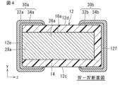
- 4 is a cross-sectional view taken along line IV-IV in FIG. 2.
- 3 is a cross-sectional view taken along line VV in FIG. 2.
- FIG. 3 is an enlarged schematic view of A in FIG. 2 .
- FIG. 3 is an enlarged schematic view showing the distribution of ceramic grains in A of FIG. 2 .
- FIG. 4 is an enlarged schematic view of B in FIG. 3 .
- 1A is a cross-sectional view taken along line II-II in FIG.
- FIG. 1 showing a structure in which a counter electrode portion of an internal electrode layer of a multilayer ceramic capacitor according to an embodiment of the present invention is divided into two
- (b) is a cross-sectional view taken along line II-II in FIG. 1 showing a structure in which a counter electrode portion of an internal electrode layer of a multilayer ceramic capacitor according to an embodiment of the present invention is divided into three
- (c) is a cross-sectional view taken along line II-II in FIG. 1 showing a structure in which a counter electrode portion of an internal electrode layer of a multilayer ceramic capacitor according to an embodiment of the present invention is divided into four.
- Multilayer Ceramic Capacitor As an example of a multilayer ceramic electronic component according to an embodiment of the present invention, a multilayer ceramic capacitor will be described.
- FIG. 1 is an external perspective view showing an example of a multilayer ceramic capacitor as a multilayer ceramic electronic component according to an embodiment of the present invention.
- FIG. 2 is a cross-sectional view taken along line II-II in FIG. 1.
- FIG. 3 is a cross-sectional view taken along line III-III in FIG. 1.
- FIG. 4 is a cross-sectional view taken along line IV-IV in FIG. 2.
- FIG. 5 is a cross-sectional view taken along line V-V in FIG. 2.
- the multilayer ceramic capacitor 10 includes a rectangular parallelepiped laminate 12 and external electrodes 30 arranged at both ends of the laminate 12.
- the laminate 12 has a plurality of laminated ceramic layers 14 and a plurality of internal electrode layers 16 laminated on the ceramic layers 14. Furthermore, the laminate 12 has a first main surface 12a and a second main surface 12b facing in a height direction (stacking direction) x, a first side surface 12c and a second side surface 12d facing in a width direction y perpendicular to the height direction x, and a first end surface 12e and a second end surface 12f facing in a length direction z perpendicular to the height direction x and the width direction y.
- the corners and ridges of this laminate 12 are rounded. The corners are the portions where three adjacent faces of the laminate intersect, and the ridges are the portions where two adjacent faces of the laminate intersect.
- unevenness or the like may be formed on a part or all of the first main surface 12 a and the second main surface 12 b, the first side surface 12 c and the second side surface 12 d, and the first end surface 12 e and the second end surface 12 f.
- the ceramic layers 14 and the internal electrode layers 16 are stacked in the height direction x.
- the laminate 12 has an outer layer section surrounding the inner layer section 18.
- the outer layer section has a first main surface side outer layer section 20a located on the first main surface 12a side, a second main surface side outer layer section 20b located on the second main surface 12b side, a first side surface side outer layer section 22a located on the first side surface 12c side, a second side surface side outer layer section 22b located on the second side surface 12d side, a first end surface side outer layer section 24a located on the first end surface 12e side, and a second end surface side outer layer section 24b located on the second end surface 12f side.
- the outer layer section will be described later.
- the laminated ceramic electronic component functions as a piezoelectric component when a piezoelectric ceramic material is used for the ceramic layers 14.
- piezoelectric ceramic materials include PZT (lead zirconate titanate) ceramic materials.
- the multilayer ceramic electronic component functions as a thermistor when a semiconducting ceramic material is used for the ceramic layers 14.
- semiconducting ceramic materials include spinel ceramic materials.
- the multilayer ceramic electronic component functions as an inductor. When functioning as an inductor, the internal electrode layers 16 become coil-shaped conductors.
- magnetic ceramic materials include ferrite ceramic materials.
- the laminate 12 has a first side outer layer portion 22a located on the first side 12c side and formed from a plurality of ceramic layers 14 located between the first side 12c and the outermost surface of the inner layer portion 18 on the first side 12c side.
- the laminate 12 has a second side outer layer portion 22b located on the second side 12d side and formed from a plurality of ceramic layers 14 located between the second side 12d and the outermost surface of the inner layer portion 18 on the second side 12d side.
- the laminate 12 has a first end face side outer layer portion 24a located on the first end face 12e side and formed from a plurality of ceramic layers 14 located between the first end face 12e and the outermost surface of the inner layer portion 18 on the first end face 12e side.
- the laminate 12 has a second end face side outer layer portion 24b located on the second end face 12f side and formed from a plurality of ceramic layers 14 located between the second end face 12f and the outermost surface of the inner layer portion 18 on the second end face 12f side.
- the ceramic layer 14 does not have to be an assembly of multiple sheets, and may have a single-layer structure.
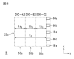
- FIG. 6 is an enlarged schematic diagram of A in FIG. 2.
- FIG. 7 is an enlarged schematic diagram showing the distribution of ceramic grains in A in FIG. 2.
- the ceramic layers 14 constituting the outer layer parts such as the first main surface side outer layer part 20a and the second main surface side outer layer part 20b are formed from the same dielectric ceramic material as the ceramic layers 14 of the inner layer part 18.
- the outer layer parts may be formed from a material different from that of the ceramic layers 14 of the inner layer part 18.
- the segregation portion of the ceramic layers 14 of the outer layer parts located closest to the first internal electrode layer 16a and the second internal electrode layer 16b is larger than the segregation portion of Si of the ceramic layers 14 of the outer layer parts other than the segregation portion. This can improve the flexural strength from the height direction x side of the multilayer ceramic capacitor 10.
- the thickness t1 of the first main surface side outer layer 20a and the second main surface side outer layer 20b after firing is 15 ⁇ m or more and 60 ⁇ m or less.
- the thickness t1 in the height direction x of either the first main surface side outer layer portion 20a or the second main surface side outer layer portion 20b is 3% or more of the thickness in the height direction x of the laminate 12.
- the first main surface side outer layer portion 20a and the second main surface side outer layer portion 20b are further described below.
- the first main surface side outer layer portion 20a has, in order from the first main surface 12a toward the inner layer portion 18, a first region 40a, a second region 40b, and a third region 40c.
- the average grain size D50 of the ceramic grains constituting the ceramic layer 14 located in the first region 40a is defined as A1.
- the average grain size D50 of the ceramic grains constituting the ceramic layer 14 located in the second region 40b is defined as B1.
- the average grain size D50 of the ceramic grains constituting the ceramic layer 14 located in the third region 40c is defined as C1.
- the relationship is C1 ⁇ A1 ⁇ B1.
- A1, B1, C1 may simply be referred to as average grain sizes A1, B1, C1, or A1, B1, C1.
- the above configuration makes it possible to suppress the occurrence of cracks, suppress the propagation of cracks into the inner layer portion 18, and improve high-temperature reliability by the first main surface side outer layer portion 20a.
- the specific features are as follows.
- the unevenness of the outer surface of the outer layer i.e., the outer surface of the laminate 12 can be reduced compared to the case where the average grain size A1 in the first region 40a > the average grain size B1 in the second region 40b in the first region 40a and the second region 40b.
- the average grain size A1 in the first region 40a which is the outermost layer of the outer layer, so that it is not the largest among the first to third regions 40a to 40c, the unevenness of the outer surface of the outer layer caused by the large average grain size can be reduced. Therefore, the uneven parts where stress is likely to concentrate can be reduced, and as a result, stress concentration can be suppressed and the occurrence of cracks can be suppressed.
- the average grain size A1 in the first region 40a is smaller than the average grain size B1 in the second region 40b, the number of grain boundaries decreases from the first region 40a to the second region 40b, that is, from the outer surface of the outer layer portion to the inner layer portion 18. Furthermore, since the average grain size B1 in the second region 40b is the largest among the first to third regions 40a to 40c, the number of grain boundaries is the smallest in the second region 40b. Therefore, since the escape route for the crack decreases from the first region 40a to the second region 40b, even if a crack occurs on the outer surface of the first region 40a and within the first region 40a, the existence of the second region 40b can prevent the crack from further extending to the third region 40c. Therefore, the crack can be prevented from extending to the inner layer portion 18, which improves the moisture resistance reliability and prevents short circuit defects.
- the average particle size C1 in the third region 40c closest to the inner layer portion 18 is adjusted to be the smallest among the first to third regions 40a to 40c. Therefore, the smoothness of the inner surface of the inner layer portion 18 side of the outer layer portion in contact with the internal electrode layer 16 can be improved. In addition, by improving the smoothness of the inner surface of the inner layer portion 18 side of the outer layer portion in contact with the internal electrode layer 16, the smoothness of the inner electrode layer 16 in contact with the outer layer portion and the ceramic layer 14 in contact with the internal electrode layer 16 in contact with the outer layer portion can also be improved. This makes it possible to suppress the formation of a thin portion in the ceramic layer 14 located in the inner layer portion 18 closest to the outer layer portion.
- the present invention can prevent the formation of thin portions in the ceramic layer 14 located in the inner layer portion closest to the outer layer portion, thereby suppressing electric field concentration and improving the reliability of the multilayer ceramic capacitor 10.
- Stress may be applied to the multilayer ceramic capacitor 10 in the following cases, for example.
- the multilayer ceramic capacitor 10 may be subjected to stress due to the impact.
- a mounting board on which the multilayer ceramic capacitor 10 is mounted thermally expands and contracts due to a thermal cycle, a flexural stress is generated in the mounting board, and this flexural stress may be applied to the multilayer ceramic capacitor 10.
- the ceramic grains constituting the ceramic layer 14 in the first region 40a are preferably stacked in a plurality of pieces in the height direction x.
- the ceramic grains constituting the ceramic layer 14 in the second region 40b are preferably stacked in a plurality of pieces in the height direction x.
- the ceramic grains constituting the ceramic layer 14 in the third region 40c are preferably stacked in a plurality of pieces in the height direction x. This makes it possible to more effectively suppress the occurrence of cracks, suppress the propagation of cracks to the inner layer portion 18, and improve high-temperature reliability.
- the first region 40a since a plurality of relatively small grains are stacked in the first region 40a, it is easy to reduce unevenness on the outer surface of the laminate 12, and it is easy to suppress the occurrence of cracks. Furthermore, since a plurality of relatively large grains are stacked in the second region 40b, it is possible to secure a relatively large area with few grain boundaries, and it is possible to suppress the propagation of cracks to the inner layer portion 18. In addition, since multiple relatively small grains are stacked in the third region 40c, the smoothness of the inner surface of the inner layer portion 18 side of the outer layer portion that contacts the internal electrode layer 16 can be improved, thereby improving the high-temperature reliability of the multilayer ceramic capacitor 10.
- the average grain sizes A1, B1, and C1 can be measured using a scanning electron microscope (SEM). Specifically, first, a cross section is polished from the first side surface 12c or the second side surface 12d of the multilayer ceramic capacitor 10 to the center of the multilayer ceramic capacitor 10 in the width direction y to expose the LT surface. Next, in the exposed LT surface, a field of view is set at a magnification such that the first region 40a, the second region 40b, and the third region 40c are contained within one field of view in the first main surface side outer layer portion 20a. Then, SEM images of the ceramic grains in the ceramic layer 14 in the first region 40a, the second region 40b, and the third region 40c are captured under a condition of an acceleration voltage of 15 kV.
- SEM scanning electron microscope
- image processing software is used to recognize the edges of all ceramic grains in the first region 40a, the second region 40b, and the third region 40c, and the cross-sectional area of the grains is calculated. From this cross-sectional area, the circle equivalent diameter is calculated as the grain diameter. At this time, the diameters of all ceramic grains included within the imaged range are measured, excluding grains that are missing and are imaged. Finally, the D50 values of the first region 40a, the second region 40b, and the third region 40c measured in the first main surface side outer layer portion 20a are averaged to calculate the average grain diameters A1, B1, and C1 of the first region 40a, the second region 40b, and the third region 40c. Note that if the average grain diameters A1, B1, and C1 can be calculated with a certain degree of precision, the diameters of some grains, rather than all ceramic grains included within the imaged range, may be measured.
- the thickness of the first main surface side outer layer portion 20a in the height direction x is t1, and the thicknesses of the regions 40a to 40c in the height direction x in the first main surface side outer layer portion 20a are ta1, tb1, and tc1.
- the thickness ta1 of the first region 40a on the first main surface 12a side in the height direction x is preferably 10% to 25% of the thickness t1 of the first main surface side outer layer portion 20a in the height direction x.
- the thickness tb1 of the second region 40b on the first main surface 12a side in the height direction x is preferably 50% to 80% of the thickness t1 of the first main surface side outer layer portion 20a in the height direction x.
- the thickness tc1 of the third region 40c on the first main surface 12a side in the height direction x is preferably 10% to 25% of the thickness t1 of the first main surface side outer layer portion 20a in the height direction x.
- the thickness ta1 in the height direction x of the first region 40a on the first main surface 12a side is preferably 10% to 25% of the thickness t1 in the height direction x of the outer layer portion 20a on the first main surface side. This makes it possible to suppress the occurrence of cracks and to suppress the cracks from extending to the inner layer portion 18.
- the average particle size B1 of the ceramic grains in the second region 40b is the largest among the first to third regions 40a to 40c, which tends to affect the smoothness of the outer surface of the outer layer portion.
- the number of irregularities increases and the smoothness of the outer surface of the outer layer portion (the outer surface of the first region 40a) decreases, which tends to concentrate stress in the irregular parts and makes it easier for cracks to occur due to external stress.
- the thickness ta1 of the first region 40a on the first main surface 12a side in the height direction x exceeds 25% of the thickness t1 of the first main surface side outer layer portion 20a in the height direction x, the force of extension of the cracks generated on the outer surface of the first region 40a and in the first region 40a will increase to extend the first region 40a, which has a certain thickness, and it may be difficult to stop the extension of the cracks in the second region 40b.
- the effect of the second region 40b in suppressing the extension of cracks generated on the outer surface of the first region 40a and in the first region 40a, etc. will decrease, and the cracks generated on the outer surface of the outer layer portion may extend to the first region 40a, the second region 40b, and the third region 40c of the outer layer portion, and even to the inner layer portion 18.
- the thickness tb1 in the height direction x of the second region 40b on the first main surface 12a side is 50% to 80% of the thickness t1 in the height direction x of the outer layer portion 20a on the first main surface side. This makes it possible to prevent cracks from extending to the inner layer portion 18, and to improve the smoothness of the outer surface of the outer layer portion and the inner surface of the outer layer portion on the inner layer portion 18 side.
- the thickness tb1 in the height direction x of the second region 40b on the first main surface 12a side is less than 50% of the thickness t1 in the height direction x of the first main surface side outer layer portion 20a, the effect of the second region 40b in suppressing the extension of cracks that have occurred on the outer surface of the first region 40a and within the first region 40a, etc., is reduced. Therefore, the cracks may extend to the first region 40a, the second region 40b, and the third region 40c of the outer layer portion, and even to the inner layer portion 18.
- the thickness tb1 of the second region 40b on the first main surface 12a side in the height direction x exceeds 80% of the thickness t1 of the first main surface side outer layer portion 20a in the height direction x, either the thickness ta1 or tc1 of the first region 40a and the third region 40c in the height direction x falls below the lower limit (25% of the thickness t1 of the first main surface side outer layer portion 20a in the height direction x).
- the average particle size A1 of the ceramic grains of the first region 40a tends to affect the smoothness of the outer surface of the outer layer portion.
- the smoothness of the outer surface of the outer layer portion decreases and the unevenness increases, so that stress tends to concentrate on the uneven parts, and cracks due to external stress tend to occur.
- the average particle size B1 of the ceramic grains in the second region 40b is likely to affect the smoothness of the inner surface of the inner layer portion 18 side of the outer layer portion in contact with the internal electrode layer 16.
- the thickness tc1 in the height direction x of the third region 40c on the first main surface 12a side is preferably 10% to 25% of the thickness t1 in the height direction x of the outer layer portion 20a on the first main surface side. This can improve the smoothness of the inner surface of the outer layer portion on the inner layer portion 18 side and can prevent cracks from extending to the inner layer portion 18.
- the average particle size B1 of the ceramic grains in the second region 40b tends to affect the smoothness of the inner surface of the inner layer portion 18 side of the outer layer portion in contact with the internal electrode layer 16.
- the smoothness of the inner surface of the inner layer portion 18 side of the outer layer portion in contact with the internal electrode layer 16 is easily affected not only on the inner surface of the inner layer portion 18 side of the outer layer portion in contact with the internal electrode layer 16, but also on the internal electrode layer 16 in contact with the outer layer portion and the ceramic layer 14 in contact with the internal electrode layer 16 in contact with the outer layer portion. Therefore, a thin portion is formed in the ceramic layer 14 located in the inner layer portion 18 closest to the outer layer portion, and when a voltage is applied to the multilayer ceramic capacitor 10, electric field concentration is likely to occur in the thin portion of the ceramic layer 14 located in the inner layer portion 18 closest to the outer layer portion, and deterioration due to electrical resistance may occur.
- the thickness tc1 in the height direction x of the third region 40c on the first main surface 12a side exceeds 25% of the thickness t1 in the height direction x of the first main surface side outer layer portion 20a
- the thickness tc1 of the third region 40c on the first main surface 12a side becomes thick. Since the average grain size C1 of the ceramic grains in the third region 40c is smaller than those in the first region 40a and the second region 40b, the number of grain boundaries of the ceramic grains increases by the amount of increase in the thickness of the third region 40c. Therefore, cracks that occur on the outer surface of the outer layer and cracks that occur inside the outer layer tend to propagate in the third region 40c and may propagate into the inner layer 18.
- the thickness t1 of the first main surface side outer layer 20a and the thicknesses ta1, tb1, and tc1 of each of the regions 40a to 40c are measured by capturing an SEM image in the same manner as when measuring the average particle sizes A1 to C1 of each of the regions 40a to 40c.
- the thickness t1 of the first main surface side outer layer 20a and the thicknesses ta1, tb1, and tc1 of the first region 40a, second region 40b, and third region 40c in the first main surface side outer layer 20a are measured from this SEM image.
- the porosity refers to the proportion of voids in a target region.
- the porosity of the first main surface side outer layer portion 20a is measured by the following method. First, the cross section of the multilayer ceramic capacitor 10 is polished from the first side surface 12c or the second side surface 12d to the center of the multilayer ceramic capacitor 10 in the width direction y to expose the LT surface. Next, the exposed LT surface is subjected to surface precision polishing by focused ion beam (FIB) processing. Then, an SEM image of the cross section of the polished first main surface side outer layer portion 20a is captured.
- FIB focused ion beam
- the average grain sizes A1, B1, C1 of the ceramic grains in the first region 40a, the second region 40b, and the third region 40c are preferably set as follows: 200 nm ⁇ A1 ⁇ 350 nm is preferable; 350 nm ⁇ B1 ⁇ 500 nm is preferable; and 100 nm ⁇ C1 ⁇ 200 nm is preferable.
- the average grain size A1 of the ceramic grains constituting the ceramic layer 14 located in the first region 40a is smaller than 200 nm, the number of grain boundaries increases too much, making it easier for cracks to occur.
- the average grain size A1 of the ceramic grains constituting the ceramic layer 14 located in the first region 40a is larger than 350 nm, the unevenness on the outer surface of the first main surface side outer layer portion 20a becomes too large. Therefore, stress tends to concentrate in these uneven parts, making it easier for cracks to occur.
- the average grain size B1 of the ceramic grains constituting the ceramic layer 14 located in the second region 40b becomes smaller than 350 nm, the number of grain boundaries increases, and the number of escape routes for cracks increases. Therefore, the effect of the second region 40b in suppressing the extension of cracks that occur on the outer surface of the first region 40a and within the first region 40a, etc., decreases.
- the average grain size B1 of the ceramic grains constituting the ceramic layer 14 located in the second region 40b becomes larger than 500 nm, the compressive stress inside the outer layer portion acts in a direction that reduces the effect of suppressing the extension of cracks by the second region 40b, which is inside the outer layer portion, may decrease.
- the smoothness of the inner surface on the inner layer portion 18 side of the outer layer portion that is in contact with the internal electrode layer 16 in the third region 40c may decrease.
- the smoothness of the inner surface of the inner layer portion 18 of the outer layer portion in contact with the internal electrode layer 16 may decrease, not only in the inner surface of the inner layer portion 18 of the outer layer portion in contact with the internal electrode layer 16, but also in the inner electrode layer 16 in contact with the outer layer portion and the ceramic layer 14 in contact with the inner electrode layer 16 in contact with the outer layer portion.
- the second main surface side outer layer portion 20b has the same configuration as the first main surface side outer layer portion 20a.
- the second main surface side outer layer portion 20b has a first region 40a, a second region 40b, and a third region 40c in this order from the second main surface 12b toward the inner layer portion 18.
- the second main surface side outer layer portion 20b also has the following relationship: average grain size C1 of the ceramic grains in the third region 40c ⁇ average grain size A1 of the ceramic grains in the first region 40a ⁇ average grain size B1 of the ceramic grains in the second region 40b.
- the second main surface side outer layer portion 20b can suppress the occurrence of cracks, suppress the extension of cracks to the inner layer portion 18, improve high-temperature reliability, and the like.
- the average particle sizes A1, B1, and C1 of the second main surface side outer layer portion 20b are also measured in the same manner as described above.
- the ceramic grains constituting the ceramic layer 14 in each of the first region 40a, the second region 40b, and the third region 40c of the second main surface side outer layer portion 20b are stacked in a plurality of pieces in the height direction x.
- the thickness of the second main surface side outer layer portion 20b in the height direction x is t1
- the thicknesses of the regions 40a to 40c in the second main surface side outer layer portion 20b in the height direction x are ta1, tb1, and tc1
- the relationship between the thicknesses ta1, tb1, and tc1 and the thickness t1 is the same as that of the first main surface side outer layer portion 20a.
- the thickness ta1 in the height direction x of the first region 40a on the second main surface 12b side is preferably 10% to 25% of the thickness t1 in the height direction x of the second main surface side outer layer portion 20b.
- the thickness tb1 in the height direction x of the second region 40b on the second main surface 12b side is preferably 50% to 80% of the thickness t1 in the height direction of the second main surface side outer layer portion 20b.
- the thickness tc1 in the height direction x of the third region 40c on the second main surface 12b side is preferably 10% to 25% of the thickness t1 in the height direction x of the second main surface side outer layer portion 20b, thereby achieving the same effects as those of the first main surface side outer layer portion 20a described above.
- the thickness t1 of the second main surface side outer layer 20b and the thicknesses ta1, tb1, and tc1 in each of the regions 40a to 40c of the second main surface side outer layer 20b are also measured in the same manner as described above.
- the thickness t1 in the height direction x of the first main surface side outer layer portion 20a may be different from the thickness t1 in the height direction x of the second main surface side outer layer portion 20b. Also, the thicknesses ta1, tb1, tc1 in the height direction x of the first region 40a, the second region 40b, and the third region 40c on the first main surface 12a side may be different from the thicknesses ta1, tb1, tc1 in the height direction x of the first region 40a, the second region 40b, and the third region 40c on the second main surface 12b side.
- the second main surface side outer layer portion 20b preferably has voids.
- the porosity of the second main surface side outer layer portion 20b is preferably 0.5% or more and 2.5% or less. This provides the same effects as the first main surface side outer layer portion 20a described above.
- the method for calculating the porosity of the second main surface side outer layer portion 20b is the same as above. It is not necessary that the porosity of the first main surface side outer layer portion 20a and the second main surface side outer layer portion 20b be the same, and the porosity of one of them may be larger or smaller.
- the average particle sizes A1, B1, C1 of the ceramic grains in the first region 40a, the second region 40b, and the third region 40c are preferably set as follows: 200 nm ⁇ A1 ⁇ 350 nm or less is preferable; 350 nm ⁇ B1 ⁇ 500 nm or less is preferable; and 100 nm ⁇ C1 ⁇ 200 nm or less is preferable. This provides the same effects as those of the first main surface side outer layer portion 20a described above.
- FIG. 8 is an enlarged schematic diagram of B in FIG. 3.
- the ceramic layers 14 constituting the outer layer parts such as the first side outer layer part 22a and the second side outer layer part 22b are formed from the same dielectric ceramic material as the ceramic layers 14 of the inner layer part 18.
- the outer layer parts may be formed from a material different from that of the ceramic layers 14 of the inner layer part 18.
- the segregation portion of the ceramic layers 14 of the outer layer parts located closest to the first internal electrode layer 16a and the second internal electrode layer 16b is larger than the segregation portion of Si of the ceramic layers 14 of the outer layer parts other than the segregation portion. This can improve the flexural strength from the width direction y side of the multilayer ceramic capacitor 10.
- the thickness of the first side outer layer 22a and the second side outer layer 22b after firing is 15 ⁇ m or more and 200 ⁇ m or less.
- the thickness t2 in the width direction y of either the first side outer layer portion 22a or the second side outer layer portion 22b is 3% or more of the thickness in the width direction y of the laminate 12.
- the first side outer layer 22a and the second side outer layer 22b are further described below.
- the first side outer layer portion 22a has, in order from the first side 12c toward the inner layer portion 18, a fourth region 50a, a fifth region 50b, and a sixth region 50c.
- the average grain size D50 of the ceramic grains constituting the ceramic layer 14 located in the fourth region 50a is A2.
- the average grain size D50 of the ceramic grains constituting the ceramic layer 14 located in the fifth region 50b is B2.
- the average grain size D50 of the ceramic grains constituting the ceramic layer 14 located in the sixth region 50c is C2.
- the relationship is C2 ⁇ A2 ⁇ B2.
- A2, B2, C2 may be simply referred to as average grain sizes A2, B2, C2, or A2, B2, C2.
- the above configuration makes it possible to suppress the occurrence of cracks, suppress the propagation of cracks into the inner layer portion 18, and improve high-temperature reliability by the first side outer layer portion 22a.
- the specific features are as follows.
- the unevenness of the outer surface of the outer layer i.e., the outer surface of the laminate 12 can be reduced compared to the case where the average grain size A2 in the fourth region 50a > the average grain size B2 in the fifth region 50b in the fourth and fifth regions 50a and 50b.
- the average grain size A2 in the fourth region 50a which is the outermost layer of the outer layer, so that it is not the largest among the fourth to sixth regions 50a to 50c, the unevenness of the outer surface of the outer layer caused by the large average grain size can be reduced. Therefore, the uneven parts where stress is likely to concentrate can be reduced, and as a result, stress concentration can be suppressed and the occurrence of cracks can be suppressed.
- the average grain size A2 in the fourth region 50a is smaller than the average grain size B2 in the fifth region 50b, the number of grain boundaries decreases from the fourth region 50a to the fifth region 50b, that is, from the outer surface of the outer layer portion to the inner layer portion 18. Furthermore, since the average grain size B2 in the fifth region 50b is the largest among the fourth to sixth regions 50a to 50c, the fifth region 50b has the fewest grain boundaries. Therefore, since the escape route for cracks decreases from the fourth region 50a to the fifth region 50b, even if cracks occur on the outer surface of the fourth region 50a and within the fourth region 50a, the existence of the fifth region 50b can prevent the cracks from further extending to the sixth region 50c. Therefore, the cracks can be prevented from extending to the inner layer portion 18, which can improve the moisture resistance reliability and prevent short circuit defects.
- the average particle size C2 in the sixth region 50c closest to the inner layer portion is adjusted to be the smallest among the fourth to sixth regions 50a to 50c. Therefore, the smoothness of the inner surface of the inner layer portion 18 side of the outer layer portion in contact with the internal electrode layer 16 can be improved. In addition, by improving the smoothness of the inner surface of the inner layer portion 18 side of the outer layer portion in contact with the internal electrode layer 16, the smoothness of the inner electrode layer 16 in contact with the outer layer portion and the ceramic layer 14 in contact with the internal electrode layer 16 in contact with the outer layer portion can also be improved.
- the ceramic grains constituting the ceramic layer 14 in the fourth region 50a are stacked in a plurality of pieces in the width direction y. It is also preferable that the ceramic grains constituting the ceramic layer 14 in the fifth region 50b are stacked in a plurality of pieces in the width direction y. It is also preferable that the ceramic grains constituting the ceramic layer 14 in the sixth region 50c are stacked in a plurality of pieces in the width direction y. This makes it possible to more effectively suppress the occurrence of cracks, suppress the extension of cracks to the inner layer portion 18, and improve high-temperature reliability.
- the average grain sizes A2, B2, and C2 can be measured using a scanning electron microscope (SEM). Specifically, first, a cross section is polished from the first main surface 12a or the second main surface 12b of the multilayer ceramic capacitor 10 to the center of the multilayer ceramic capacitor 10 in the height direction x to expose the WT surface. Next, in the exposed WT surface, a field of view is set at a magnification such that the fourth region 50a, the fifth region 50b, and the sixth region 50c are contained within one field of view in the first side outer layer portion 22a. Then, SEM images of the ceramic grains in the ceramic layer 14 in the fourth region 50a, the fifth region 50b, and the sixth region 50c are captured under a condition of an acceleration voltage of 15 kV.
- SEM scanning electron microscope
- image processing software is used to recognize the edges of all the ceramic grains in the fourth region 50a, the fifth region 50b, and the sixth region 50c, and the cross-sectional area of the grains is calculated. From this cross-sectional area, the circle equivalent diameter is calculated as the grain diameter. At this time, the diameters of all the ceramic grains included in the imaged range are measured, excluding the grains that are missing in the image. Finally, the D50 values of the fourth region 50a, the fifth region 50b, and the sixth region 50c measured in the second side outer layer portion 22b are averaged to calculate the average grain diameters A2, B2, and C2 of the fourth region 50a, the fifth region 50b, and the sixth region 50c. Note that if the average grain diameters A2, B2, and C2 can be calculated with a certain degree of precision, the diameters of some of the grains, rather than all of the ceramic grains included in the imaged range, may be measured.
- the thickness in the width direction y of the first side surface side outer layer portion 22a is t2, and the thicknesses in the width direction y of each of the regions 50a to 50c in the first side surface side outer layer portion 22a are ta2, tb2, and tc2.
- the thickness in the width direction y of the fourth region 50a on the first side surface 12c side is preferably 10% to 25% of the thickness in the width direction y of the first side surface side outer layer portion 22a.
- the thickness in the width direction y of the fifth region 50b on the first side surface 12c side is preferably 50% to 80% of the thickness in the width direction y of the first side surface side outer layer portion 22a.
- the thickness in the width direction y of the sixth region 50c on the first side surface 12c side is preferably 10% to 25% of the thickness in the width direction y of the first side surface side outer layer portion 22a.
- the thickness ta2 in the width direction y of the fourth region 50a on the first side surface 12c side is preferably 10% to 25% of the thickness t2 in the width direction y of the outer layer portion 22a on the first side surface side. This makes it possible to suppress the occurrence of cracks and to suppress the cracks from extending to the inner layer portion 18.
- the average particle size B2 of the ceramic grains in the fifth region 50b is the largest among the fourth to sixth regions 50a to 50c, which tends to affect the smoothness of the outer surface of the outer layer portion.
- the number of irregularities increases and the smoothness of the outer surface of the outer layer portion (the outer surface of the fourth region 50a) decreases, which tends to concentrate stress in the irregular parts and to cause cracks due to external stress.
- the thickness ta2 of the fourth region 50a on the first side surface 12c side in the width direction y exceeds 25% of the thickness t2 of the first side surface side outer layer portion 22a in the width direction y, the force of extension of the cracks generated on the outer surface of the fourth region 50a and in the fourth region 50a, etc., will increase in order to extend the fourth region 50a, which has a certain thickness, and it may be difficult to stop the extension of the cracks in the fifth region 50b.
- the effect of the fifth region 50b in suppressing the extension of the cracks generated on the outer surface of the fourth region 50a and in the fourth region 50a, etc. will decrease, and the cracks generated on the outer surface of the outer layer portion may extend to the fourth region 50a, fifth region 50b, and sixth region 50c of the outer layer portion, and even to the inner layer portion 18.
- the thickness tb2 in the width direction y of the fifth region 50b on the first side surface 12c side is 50% or more and 80% or less of the thickness t2 in the width direction y of the outer layer portion 22a on the first side surface side. This makes it possible to suppress the crack from extending to the inner layer portion 18, and to improve the smoothness of the outer surface of the outer layer portion and the inner surface of the outer layer portion on the inner layer portion 18 side.
- the thickness tb2 in the width direction y of the fifth region 50b on the first side surface 12c side is less than 50% of the thickness t2 in the width direction y of the first side surface side outer layer portion 22a, the effect of the fifth region 50b in suppressing the extension of cracks that have occurred on the outer surface of the fourth region 50a and within the fourth region 50a, etc., is reduced. Therefore, the cracks may extend to the fourth region 50a, the fifth region 50b, and the sixth region 50c of the outer layer portion, and even to the inner layer portion 18.
- the thickness tb2 in the width direction y of the fifth region 50b on the first side surface 12c side exceeds 80% of the thickness t2 in the width direction y of the first side surface side outer layer portion 22a
- either the thickness ta2 or tc2 in the width direction y of the fourth region 50a and the sixth region 50c falls below the lower limit (25% of the thickness t2 in the width direction y of the first side surface side outer layer portion 22a).
- the average particle size A2 of the ceramic grains in the fourth region 50a tends to affect the smoothness of the outer surface of the outer layer portion.
- the smoothness of the outer surface of the outer layer portion decreases and the unevenness increases, so that stress tends to concentrate on the uneven parts, and cracks due to external stress tend to occur.
- the average particle size B2 of the ceramic grains in the fifth region 50b is likely to affect the smoothness of the inner surface of the inner layer portion 18 side of the outer layer portion in contact with the internal electrode layer 16.
- the thickness tc2 in the width direction y of the sixth region 50c on the first side surface 12c side is preferably 10% to 25% of the thickness t2 in the width direction y of the outer layer portion 22a on the first side surface side. This improves the smoothness of the inner surface of the outer layer portion on the inner layer portion 18 side, and also prevents cracks from extending to the inner layer portion 18.
- the average particle size B2 of the ceramic grains in the fifth region 50b is likely to affect the smoothness of the inner surface of the inner layer portion 18 side of the outer layer portion in contact with the internal electrode layer 16.
- the thickness tc2 in the width direction y of the sixth region 50c on the first side surface 12c side exceeds 25% of the thickness t2 in the width direction y of the first side surface side outer layer portion 22a
- the thickness tc2 of the sixth region 50c on the first side surface 12c side becomes thicker. Since the average grain size C2 of the ceramic grains in the sixth region 50c is smaller than those in the fourth region 50a and the fifth region 50b, the number of grain boundaries of the ceramic grains increases by the amount of increase in the thickness of the sixth region 50c. Therefore, cracks that occur on the outer surface of the outer layer and cracks that occur inside the outer layer tend to propagate in the sixth region 50c and may propagate into the inner layer 18.
- the thickness t2 of the first side outer layer 22a and the thicknesses ta2, tb2, and tc2 of each of the regions 50a-50c are measured by capturing an SEM image in the same manner as when measuring the average particle sizes A2-C2 of each of the regions 50a-50c.
- the thickness t2 of the first side outer layer 22a and the thicknesses ta2, tb2, and tc2 of the fourth region 50a, the fifth region 50b, and the sixth region 50c in the first side outer layer 22a are measured from this SEM image.
- the first side surface outer layer portion 22a preferably has voids.
- the porosity of the first side surface outer layer portion 22a is preferably 0.5% or more and 2.5% or less.
- the porosity of the first side outer layer 22a By setting the porosity of the first side outer layer 22a to 0.5% or more and 2.5% or less, it is possible to prevent water from entering through the voids from the outside of the outer layer, and further to prevent water from entering the inner layer 18. In addition, it is possible to prevent stress from concentrating in the voids, which in turn prevents cracks from occurring and from propagating toward the inner layer 18.
- the method for measuring the porosity will be described below.
- the cross-section of the multilayer ceramic capacitor 10 is polished from the first main surface 12a or the second main surface 12b to the center of the multilayer ceramic capacitor 10 in the height direction x, to expose the WT surface.
- the exposed WT surface is subjected to surface precision polishing by focused ion beam (FIB) processing.
- FIB focused ion beam
- an SEM image of the cross-section of the polished first side surface outer layer portion 22a is captured.
- the porosity is calculated thereafter in the same manner as the porosity of the first main surface outer layer portion 20a.
- the average particle sizes A2, B2, C2 of the ceramic grains in the fourth region 50a, the fifth region 50b, and the sixth region 50c are preferably set as follows: 200 nm ⁇ A2 ⁇ 350 nm is preferable; 350 nm ⁇ B2 ⁇ 500 nm is preferable; and 100 nm ⁇ C2 ⁇ 200 nm is preferable.
- the average grain size A2 of the ceramic grains constituting the ceramic layer 14 located in the fourth region 50a is smaller than 200 nm, the number of grain boundaries increases too much, making it easier for cracks to occur.
- the average grain size A2 of the ceramic grains constituting the ceramic layer 14 located in the fourth region 50a is larger than 350 nm, the unevenness on the outer surface of the first side outer layer portion 22a becomes too large. Therefore, stress tends to concentrate in these uneven parts, making it easier for cracks to occur.
- the average grain size B2 of the ceramic grains constituting the ceramic layer 14 located in the fifth region 50b becomes smaller than 350 nm, the number of grain boundaries increases, and the number of escape routes for cracks increases. Therefore, the effect of the fifth region 50b in suppressing the extension of cracks that occur on the outer surface of the fourth region 50a and within the fourth region 50a, etc., decreases.
- the average grain size B2 of the ceramic grains constituting the ceramic layer 14 located in the fifth region 50b becomes larger than 500 nm, the compressive stress inside the outer layer portion acts in a direction that reduces the effect of suppressing the extension of cracks by the fifth region 50b, which is inside the outer layer portion, may decrease.
- the average grain size C2 of the ceramic grains constituting the ceramic layer 14 located in the sixth region 50c becomes smaller than 100 nm, the number of grain boundaries in the sixth region 50c increases. This increases the occurrence of internal cracks caused by the firing process in the sixth region 50c close to the internal electrode layer 16.
- an internal crack that occurs in the sixth region 50c extends to the inner layer portion 18, a crack that spans from the outer layer portion to the inner layer portion 18 occurs, and the reliability of the multilayer ceramic capacitor 10 may decrease.
- the smoothness of the inner surface on the inner layer portion 18 side of the outer layer portion that is in contact with the internal electrode layer 16 in the sixth region 50c may decrease.
- the smoothness of the inner surface of the inner layer portion 18 of the outer layer portion in contact with the internal electrode layer 16 may decrease, not only in the inner surface of the inner layer portion 18 of the outer layer portion in contact with the internal electrode layer 16, but also in the inner electrode layer 16 in contact with the outer layer portion and the ceramic layer 14 in contact with the inner electrode layer 16 in contact with the outer layer portion.
- the second side surface side outer layer portion 22b has the same configuration as the first side surface side outer layer portion 22a.
- the second side surface side outer layer portion 22b has a fourth region 50a, a fifth region 50b, and a sixth region 50c in the order from the second side surface 12d toward the inner layer portion 18.
- the second side surface side outer layer portion 22b also has the following relationship: average grain size C2 of the ceramic grains in the sixth region 50c ⁇ average grain size A2 of the ceramic grains in the fourth region 50a ⁇ average grain size B2 of the ceramic grains in the fifth region 50b.
- the second side surface side outer layer portion 22b can suppress the occurrence of cracks, suppress the extension of cracks to the inner layer portion 18, improve high-temperature reliability, and the like.
- the average particle sizes A2, B2, and C2 of the second side surface outer layer portion 22b are also measured in the same manner as described above.
- the first side surface side outer layer portion 22a and the second side surface side outer layer portion 22b can also suppress the occurrence of cracks, suppress the propagation of cracks into the inner layer portion 18, and improve high temperature reliability. Therefore, since any of the first main surface side outer layer portion 20a, the second main surface side outer layer portion 20b, the first side surface side outer layer portion 22a, and the second side surface side outer layer portion 22b can be made to face the mounting board during mounting, there is no need to select the direction.
- the ceramic grains constituting the ceramic layer 14 in each of the fourth region 50a, the fifth region 50b, and the sixth region 50c are stacked in a plurality of pieces in the width direction y.
- the thickness of the second side surface outer layer portion 22b in the width direction y is t2
- the thicknesses of the regions 50a to 50c in the second main surface outer layer portion 20b in the width direction y are ta2, tb2, and tc2
- the relationship between the thicknesses ta2, tb2, and tc2 and the thickness t2 is the same as that of the first side surface outer layer portion 22a.
- the thickness ta2 in the width direction y of the fourth region 50a on the second side surface 12d side is preferably 10% to 25% of the thickness t2 in the width direction y of the second side surface outer layer portion 22b.
- the thickness tb2 in the width direction y of the fifth region 50b on the second side surface 12d side is preferably 50% to 80% of the thickness t2 in the width direction y of the second side surface outer layer portion 22b.
- the thickness tc2 in the width direction y of the sixth region 50c on the second side surface 12d side is preferably 10% to 25% of the thickness t2 in the width direction y of the second side surface side outer layer portion 22b, thereby achieving the same effects as those of the first side surface side outer layer portion 22a described above.
- the thickness t2 of the second side outer layer 22b and the thicknesses ta2, tb2, and tc2 in each of the regions 50a to 50c of the second side outer layer 22b are also measured in the same manner as described above.
- the thickness t2 in the width direction y of the first side surface outer layer 22a may be different from the thickness t2 in the width direction y of the second side surface outer layer 22b.
- the thicknesses ta2, tb2, tc2 in the width direction y of the fourth region 50a, the fifth region 50b, and the sixth region 50c on the first side surface 12c side may be different from the thicknesses ta2, tb2, tc2 in the width direction y of the fourth region 50a, the fifth region 50b, and the sixth region 50c on the second side surface 12d side.
- the second side surface outer layer portion 22b preferably has voids.
- the porosity of the second side surface outer layer portion 22b is preferably 0.5% or more and 2.5% or less. This provides the same effects as those of the first side surface outer layer portion 22a described above.
- the method for calculating the porosity of the second side surface outer layer portion 22b is the same as above.
- the porosity of the first side surface outer layer portion 22a and the second side surface outer layer portion 22b does not need to be the same, and the porosity of one of them may be larger or smaller.
- the average particle sizes A2, B2, C2 of the ceramic grains in the fourth region 50a, the fifth region 50b, and the sixth region 50c are preferably set as follows: 200 nm ⁇ A2 ⁇ 350 nm or less is preferable; 350 nm ⁇ B2 ⁇ 500 nm or less is preferable; and 100 nm ⁇ C2 ⁇ 200 nm or less is preferable. This provides the same effects as the first side surface outer layer portion 22a described above.
- the laminate 12 has, for example, a plurality of substantially rectangular first internal electrode layers 16a and a plurality of second internal electrode layers 16b as the plurality of internal electrode layers 16.
- the plurality of first internal electrode layers 16a and the plurality of second internal electrode layers 16b are embedded so as to be alternately arranged at equal intervals with the ceramic layers 14 interposed therebetween along the height direction x of the laminate 12.
- the first internal electrode layer 16a is disposed on the multiple ceramic layers 14 and is located inside the laminate 12.
- the first internal electrode layer 16a has a first opposing electrode portion 26a that faces the second internal electrode layer 16b, and a first extraction electrode portion 28a that is located on one end side of the first internal electrode layer 16a and extends from the first opposing electrode portion 26a to the first end face 12e of the laminate 12.
- the end of the first extraction electrode portion 28a is extended to the surface of the first end face 12e and is exposed from the laminate 12.
- the shape of the first opposing electrode portion 26a of the first internal electrode layer 16a is not particularly limited, but is preferably rectangular in plan view. However, the corners in plan view may be rounded or may be formed at an angle in plan view (tapered). It may also be tapered in plan view, with a slope in either direction.
- the shape of the first extraction electrode portion 28a of the first internal electrode layer 16a is not particularly limited, but is preferably rectangular in plan view. However, the corners in plan view may be rounded or may be formed at an angle in plan view (tapered). It may also be tapered in plan view, with a slope in either direction.
- the width of the first opposing electrode portion 26a of the first internal electrode layer 16a and the width of the first extraction electrode portion 28a of the first internal electrode layer 16a may be the same, or one of them may be narrower.
- the second internal electrode layer 16b is disposed on the multiple ceramic layers 14 and is located inside the laminate 12.
- the second internal electrode layer 16b has a second opposing electrode portion 26b that faces the first internal electrode layer 16a, and a second extraction electrode portion 28b that is located on one end side of the second internal electrode layer 16b and extends from the second opposing electrode portion 26b to the second end face 12f of the laminate 12.
- the end of the second extraction electrode portion 28b is extended to the surface of the second end face 12f and is exposed from the laminate 12.
- the shape of the second opposing electrode portion 26b of the second internal electrode layer 16b is not particularly limited, but is preferably rectangular in plan view. However, the corners in plan view may be rounded or may be formed at an angle in plan view (tapered). It may also be tapered in plan view, with a slope in either direction.
- the shape of the second extraction electrode portion 28b of the second internal electrode layer 16b is not particularly limited, but is preferably rectangular in plan view. However, the corners in plan view may be rounded or may be formed at an angle in plan view (tapered). It may also be tapered in plan view, with a slope in either direction.
- the width of the second opposing electrode portion 26b of the second internal electrode layer 16b and the width of the second extraction electrode portion 28b of the second internal electrode layer 16b may be the same, or one of them may be narrower.
- the first internal electrode layer 16a and the second internal electrode layer 16b can be made of an appropriate conductive material, such as a metal such as Ni, Cu, Ag, Pd, or Au, or an alloy containing at least one of these metals, such as an Ag-Pd alloy.
- an appropriate conductive material such as a metal such as Ni, Cu, Ag, Pd, or Au, or an alloy containing at least one of these metals, such as an Ag-Pd alloy.
- each of the internal electrode layers 16, that is, the first internal electrode layer 16a and the second internal electrode layer 16b is preferably 0.2 ⁇ m or more and 2.0 ⁇ m or less, and more preferably 0.2 ⁇ m or more and 0.5 ⁇ m or less.
- the total number of the first internal electrode layers 16a and the second internal electrode layers 16b is preferably 15 or more and 1000 or less.
- Sn may also be present at the interface between the ceramic layer 14 and the internal electrode layer 16. If Sn is present, it may be present in the form of a layer parallel to the internal electrode layer 16, or it may be scattered. Sn may also be dissolved inside the internal electrode layer 16, or it may be present in the ceramic layer 14.
- the first opposing electrode portion 26a of the first internal electrode layer 16a and the second opposing electrode portion 26b of the second internal electrode layer 16b face each other via the ceramic layer 14, forming a capacitance. Therefore, a capacitance can be obtained between the first external electrode 30a to which the first internal electrode layer 16a is connected and the second external electrode 30b to which the second internal electrode layer 16b is connected, and the characteristics of a capacitor are expressed.
- the laminate 12 shown in FIG. 1 may have a floating internal electrode layer 16c that is not drawn out to either the first end face 12e or the second end face 12f, in addition to the first internal electrode layer 16a and the second internal electrode layer 16b, and the floating internal electrode layer 16c may divide the opposing electrode portion 26c into multiple parts.
- the opposing electrode portion 26c may have a two-way structure as shown in FIG. 9(a), a three-way structure as shown in FIG. 9(b), a four-way structure as shown in FIG. 9(c), or a structure of more than four parts.
- the opposing electrode portion 26c by dividing the opposing electrode portion 26c into multiple parts, multiple capacitor components are formed between the opposing internal electrode layers 16a, 16b, and 16c, and these capacitor components are connected in series. Therefore, the voltage applied to each capacitor component is reduced, and the multilayer ceramic capacitor 10 can have a high withstand voltage.
- external electrodes 30 are disposed on the first end face 12e side and the second end face 12f side of the laminate 12.
- the external electrode 30 has a first external electrode 30a and a second external electrode 30b.
- the first external electrode 30a is connected to the first internal electrode layer 16a and is disposed on at least the surface of the first end face 12e.
- the first external electrode 30a extends from the first end face 12e of the laminate 12 and is disposed on a part of the first main face 12a and a part of the second main face 12b, as well as a part of the first side face 12c and a part of the second side face 12d.
- the first external electrode 30a is electrically connected to the first lead electrode portion 28a of the first internal electrode layer 16a.
- the second external electrode 30b is connected to the second internal electrode layer 16b and is disposed on at least the surface of the second end face 12f.
- the second external electrode 30b extends from the second end face 12f and is disposed on a part of the first main face 12a and a part of the second main face 12b, as well as a part of the first side face 12c and a part of the second side face 12d.
- the second external electrode 30b is electrically connected to the second lead-out electrode portion 28b of the second internal electrode layer 16b.
- the external electrode 30 includes a base electrode layer 32 containing a metal component, and a plating layer 34 disposed on the base electrode layer 32 .
- the first external electrode 30a has a first base electrode layer 32a containing a metal component, and a first plating layer 34a disposed on the first base electrode layer 32a.
- the second external electrode 30b includes a second base electrode layer 32b containing a metal component, and a second plating layer 34b disposed on the second base electrode layer 32b.
- the first base electrode layer 32a is connected to the first internal electrode layer 16a and is disposed on the surface of the first end face 12e.
- the first base electrode layer 32a also extends from the first end face 12e and is disposed on a part of the first main face 12a and a part of the second main face 12b, as well as a part of the first side face 12c and a part of the second side face 12d.
- the first base electrode layer 32a is electrically connected to the first lead electrode portion 28a of the first internal electrode layer 16a.
- the first base electrode layer 32a is disposed only on the surface of the first end face 12e.
- the second base electrode layer 32b is connected to the second internal electrode layer 16b and is disposed on the surface of the second end face 12f.
- the second base electrode layer 32b also extends from the second end face 12f and is disposed on a part of the first main face 12a and a part of the second main face 12b, as well as a part of the first side face 12c and a part of the second side face 12d.
- the second base electrode layer 32b is electrically connected to the second lead electrode portion 28b of the second internal electrode layer 16b.
- the second base electrode layer 32b is disposed only on the surface of the second end face 12f.
- the base electrode layer 32 includes at least one selected from a baked layer, a conductive resin layer, a thin film layer, and the like.
- a baked layer a baked layer
- a conductive resin layer a thin film layer
- the baking layer includes a glass component and a metal component.
- the glass component of the baking layer may include an oxide including at least one element selected from B, Si, Ba, Mg, Al, Li, etc.
- the glass component included in the base electrode layer 32 is preferably a glass including an oxide such as silicic acid (SiO 2 ), alumina (Al 2 O 3 ), titanium oxide (TiO 2 ), barium oxide (BaO 2 ), and zirconia (ZrO 2 ).
- the glass component included in the base electrode layer 32 more preferably includes an oxide including Ba and Ti.
- the glass component included in the base electrode layer 32 is preferably a glass including barium oxide (BaO 2 ) and titanium oxide (TiO 2 ).
- the glass component included in the base electrode layer 32 is barium oxide (BaO 2 ) and titanium oxide (TiO 2 )
- such a glass component has a characteristic of having few impurities in the glass component and being soft.
- the metal component of the baked layer includes, for example, at least one selected from Cu, Ni, Ag, Pd, Ag-Pd alloy, Au, etc.
- the baked layer may be multiple layers.
- the baking layer is formed by applying a conductive paste containing a glass component and a metal component to the laminate 12 and baking it. It may be baked simultaneously with the internal electrode layer 16 and the ceramic layer 14, or may be baked after the internal electrode layer 16 and the ceramic layer 14 are baked. When the baking layer is baked simultaneously with the internal electrode layer 16 and the ceramic layer 14, it is preferable to add a ceramic component instead of a glass component to form the baking layer.
- the ceramic component may be the same type of ceramic material as the ceramic layer 14, or a different type of ceramic material.
- the ceramic component includes at least one selected from, for example, BaTiO 3 , CaTiO 3 , (Ba, Ca)TiO 3 , SrTiO 3 , CaZrO 3 , etc.
- the thickness in the length direction z connecting the first end face 12e and the second end face 12f at the center of the height direction x connecting the first main surface 12a and the second main surface 12b of the first baked layer located on the first end face 12e is preferably, for example, about 3 ⁇ m or more and 100 ⁇ m or less.
- the thickness in the length direction z connecting the first end face 12e and the second end face 12f at the center of the height direction x connecting the first main surface 12a and the second main surface 12b of the second baked layer located on the second end face 12f is preferably, for example, about 3 ⁇ m or more and 100 ⁇ m or less.
- the thickness in the height direction x connecting the first principal surface 12a and the second principal surface 12b at the center of the length direction z connecting the first end surface 12e and the second end surface 12f of the first baked layer located on a part of the first principal surface 12a and a part of the second principal surface 12b is preferably, for example, about 3 ⁇ m or more and 70 ⁇ m or less.
- the thickness in the height direction x connecting the first principal surface 12a and the second principal surface 12b at the center of the length direction z connecting the first end surface 12e and the second end surface 12f of the second baked layer located on a part of the first principal surface 12a and a part of the second principal surface 12b is preferably, for example, about 3 ⁇ m or more and 70 ⁇ m or less.
- the thickness in the width direction y connecting the first side 12c and the second side 12d at the center of the length direction z connecting the first end face 12e and the second end face 12f of the first baked layer located on a part of the first side 12c and a part of the second side 12d is preferably, for example, about 3 ⁇ m or more and 70 ⁇ m or less.
- the thickness in the width direction y connecting the first side 12c and the second side 12d at the center of the length direction z connecting the first end face 12e and the second end face 12f of the second baked layer located on a part of the first side 12c and a part of the second side 12d is preferably, for example, about 3 ⁇ m or more and 70 ⁇ m or less.
- the conductive resin layer may be a multi-layered layer.
- the conductive resin layer may be disposed on the baked layer so as to cover the baked layer, or the conductive resin layer may be disposed directly on the laminate 12 . Further explaining the case where the conductive resin layer is disposed on the baked layer, the conductive resin layer is disposed so as to cover all or a part of the base electrode layer 32 which is the baked layer.
- the conductive resin layer has a first conductive resin layer and a second conductive resin layer. The first conductive resin layer is disposed so as to cover the first base electrode layer 32a, and the second conductive resin is disposed so as to cover the second base electrode layer 32b.
- the first and second conductive resin layers are disposed on the first base electrode layer 32a and the second base electrode layer 32b located on the first end face 12e and the second end face 12f. Furthermore, it is preferable that the first and second conductive resin layers are disposed so as to reach the first main surface 12a and the second main surface 12b, and the first side surface 12c and the second side surface 12d. However, the first and second conductive resin layers may be disposed only on the first and second base electrode layers 32a and 32b located on the first and second end faces 12e and 12f. When the external electrode 30 has a plating layer 34, the conductive resin layer can be disposed between the base electrode layer 32 and the plating layer 34.
- the conductive resin layer includes a thermosetting resin and a metal. Since the conductive resin layer contains a thermosetting resin, it is more flexible than a conductive layer made of, for example, a plating film or a fired product of a conductive paste. Therefore, even if the multilayer ceramic capacitor 10 is subjected to a physical impact or an impact due to a thermal cycle, the conductive resin layer functions as a buffer layer and can prevent the multilayer ceramic capacitor 10 from cracking.
- the metal contained in the conductive resin layer may be Ag, Cu, Ni, Sn, Bi, or an alloy containing any of these.
- Metal powders whose surfaces are Ag-coated can also be used. When using metal powders whose surfaces are Ag-coated, it is preferable to use Cu, Ni, Sn, Bi or alloy powders thereof as the metal powder.
- Ag conductive metal powders are used as the conductive metal is that Ag has the lowest resistivity among metals and is therefore suitable as an electrode material, and Ag is a noble metal, so it does not oxidize and has high weather resistance.
- Ag-coated metal powders are used is that it is possible to make the base metal cheaper while maintaining the above-mentioned characteristics of Ag.
- the metal contained in the conductive resin layer may be Cu or Ni that has been subjected to an anti-oxidation treatment.
- a metal powder having a surface coated with Sn, Ni, or Cu can also be used.
- Ag, Cu, Ni, Sn, Bi, or an alloy powder thereof it is preferable to use Ag, Cu, Ni, Sn, Bi, or an alloy powder thereof as the metal powder.
- the metal contained in the conductive resin layer is preferably contained in an amount of 35 vol % or more and 75 vol % or less with respect to the total volume of the conductive resin.
- the average particle size of the metal contained in the conductive resin layer is not particularly limited, and the average particle size of the conductive filler may be, for example, about 0.3 ⁇ m or more and 10 ⁇ m or less.
- the metal contained in the conductive resin layer is mainly responsible for the electrical conductivity of the conductive resin layer. Specifically, the conductive fillers come into contact with each other to form electrical paths inside the conductive resin layer.
- the shape of the metal contained in the conductive resin layer is not particularly limited, and spherical, flat, and other shapes can be used. It is preferable to use a mixture of spherical metal powder and flat metal powder as the metal contained in the conductive resin layer.
- thermosetting resins such as epoxy resin, phenoxy resin, phenol resin, urethane resin, silicone resin, polyimide resin, etc.
- epoxy resin which has excellent heat resistance, moisture resistance, adhesion, etc., is one of the most suitable resins.
- the resin contained in the conductive resin layer is preferably contained in an amount of 25 vol % or more and 65 vol % or less with respect to the volume of the entire conductive resin.
- the conductive resin layer preferably contains a curing agent in addition to the thermosetting resin.
- a curing agent in addition to the thermosetting resin.
- various known compounds such as phenol-based, amine-based, acid anhydride-based, imidazole-based, active ester-based, and amide-imide-based compounds can be used as the curing agent for the epoxy resin.
- the conductive resin layer may also include a resin layer containing conductive particles and a thermosetting resin.
- the resin layer may be formed directly on the laminate 12 without forming a baked layer.
- the thickness of the conductive resin layer (the thickness at the thickest part) is preferably, for example, about 10 ⁇ m or more and 150 ⁇ m or less.
- the thin film layer is formed by a thin film forming method such as sputtering or vapor deposition, and is a layer of 1 ⁇ m or less in thickness in which metal particles are deposited.
- the first plating layer 34a is arranged so as to cover the first base electrode layer 32a on the first end face 12e side. Furthermore, the first plating layer 34a may be arranged so as to cover the first base electrode layer 32a on the first main surface 12a, the second main surface 12b, the first side surface 12c, and the second side surface 12d side. However, the first plating layer 34a may be arranged only on the first base electrode layer 32a on the first end face 12e side.
- the second plating layer 34b is arranged so as to cover the second base electrode layer 32b on the second end face 12f side. Furthermore, the second plating layer 34b may be arranged so as to cover the second base electrode layer 32b on the first main surface 12a, the second main surface 12b, the first side surface 12c, and the second side surface 12d side. However, the second plating layer 34b may be arranged only on the second base electrode layer 32b on the second end face 12f side.
- the first plating layer 34a and the second plating layer 34b include, for example, at least one selected from Cu, Ni, Sn, Ag, Pd, Ag-Pd alloy, Au, etc.
- the plating layer 34 may be formed of multiple layers.
- the first plating layer 34a has a two-layer structure consisting of a first lower-layer plating layer and a first upper-layer plating layer covering the first lower-layer plating layer
- the second plating layer 34b has a two-layer structure consisting of a second lower-layer plating layer and a second upper-layer plating layer covering the second lower-layer plating layer.
- the first lower-layer plating layer and the second lower-layer plating layer are Ni plating layers
- the first upper-layer plating layer and the second upper-layer plating layer are Sn plating layers.
- the first and second lower plating layers made of Ni are used to prevent the base electrode layer 32 from being eroded by solder when mounting the multilayer ceramic capacitor 10.
- the first and second upper plating layers made of Sn are used to improve the wettability of the solder when mounting the multilayer ceramic capacitor 10, making it easier to mount.
- the first and second lower plating layers made of Ni plating layers are preferably 1 ⁇ m or more and 15 ⁇ m or less.
- the first and second upper plating layers made of Sn plating layers are preferably 1 ⁇ m or more and 15 ⁇ m or less.
- the plating layer 34 is disposed so as to cover the conductive resin layer. Even in this case, the Ni plating layer, which is the lower plating layer of the plating layer 34, prevents the conductive resin layer from being eroded by the solder, and the Sn plating layer, which is the upper plating layer, improves the wettability of the solder.
- the first and second external electrodes 30a, 30b may not have the base electrode layer 32, and the plating layer 34 may be formed directly on the surface of the laminate 12. That is, the laminated ceramic capacitor 10 may have a structure in which the first end face 12e and the second end face 12f are plated to form the plating layer 34 electrically connected to the first internal electrode layer 16a or the second internal electrode layer 16b. In such a case, the plating layer 34 may be formed by plating after disposing a catalyst on the surface of the laminate 12 as a pretreatment. Either electrolytic plating or electroless plating may be used for plating. However, electroless plating has the disadvantage that a pretreatment using a catalyst or the like is required to improve the plating deposition speed, which complicates the process. Therefore, it is usually preferable to use electrolytic plating. As a plating method, it is preferable to use barrel plating.
- the reduction in the thickness of the base electrode layer 32 can be converted into a lower profile, i.e., a thinner laminate, or into the thickness of the laminate, i.e., the thickness of the effective layer portion, thereby improving the design freedom of the thickness of the laminate 12.
- the plating layer 34 includes an underlayer plating layer formed on the surface of the laminate 12, and an upper layer plating layer formed on the surface of the underlayer plating layer.
- Each of the underlayer plating layer and the upper layer plating layer preferably includes at least one metal selected from, for example, Cu, Ni, Sn, Pb, Au, Ag, Pd, Bi, Zn, or the like, or an alloy containing the metal.
- the lower plating layer is preferably formed using Ni, which has solder barrier properties
- the upper plating layer is preferably formed using Sn or Au, which has good solder wettability.
- the lower plating layer 16b is formed using Cu, which has good bonding properties with Ni.
- the upper plating layer may be formed as necessary, and the first external electrode 30a and the second external electrode 30b may each be composed of only the lower plating layer.
- the plating layer 34 may be the upper plating layer as the outermost layer, or another plating electrode may be formed on the surface of the upper plating layer.
- the thickness of each plating layer 34 arranged without providing the base electrode layer 32 is preferably 1 ⁇ m or more and 15 ⁇ m or less. Furthermore, it is preferable that the plating layer 34 does not contain glass.
- the metal ratio per unit volume of the plating layer 34 is preferably 99 volume % or more.
- the dimension in the length direction z of the multilayer ceramic capacitor 10, including the laminate 12, the first external electrode 30a, and the second external electrode 30b, is defined as dimension L.
- the dimension in the height direction x of the multilayer ceramic capacitor 10, including the laminate 12, the first external electrode 30a, and the second external electrode 30b is defined as dimension T.
- the dimension in the width direction y of the multilayer ceramic capacitor 10, including the laminate 12, the first external electrode 30a, and the second external electrode 30b, is defined as dimension W.
- the dimensions of the multilayer ceramic capacitor 10 are: L dimension in the length direction z is 0.2 mm to 1.8 mm, W dimension in the width direction y is 0.1 mm to 1.0 mm, and T dimension in the height direction x is 0.1 mm to 1.0 mm.
- the dimensions of the multilayer ceramic capacitor 10 can be measured using a microscope.
- Step 1 a dielectric sheet for the ceramic layer and a conductive paste for the internal electrode layer are prepared.
- the dielectric sheet and the conductive paste for the internal electrode layer contain a binder and a solvent.
- the binder and the solvent may be publicly known.
- Step 2 a conductive paste for the internal electrode layers is printed in a predetermined pattern on the dielectric sheet, for example by screen printing or gravure printing. This prepares a dielectric sheet on which the pattern of the first internal electrode layer is formed, and a dielectric sheet on which the pattern of the second internal electrode layer is formed.
- outer layer dielectric sheets that do not have the internal electrode layer pattern printed on them are also prepared.
- a dielectric sheet with adjusted amounts of Mn, Mg, and Si is used.
- Mn, Mg, and Si it is possible to control the sizes A1, B1, and C1, which are the average grain size D50 values of the ceramic grains that make up the ceramic layer in the first region 40a, the second region 40b, and the third region 40c of the first main surface side outer layer portion 20a and the second main surface side outer layer portion 20b.
- the movement of the liquid phase in the first main surface side outer layer portion 20a and the second main surface side outer layer portion 20b is appropriately controlled while the grains are grown, so that the average grain size D50 values A1, B1, and C1 of the ceramic grains constituting the ceramic layers in the first region 40a, the second region 40b, and the third region 40c can be realized in a desired grain size distribution.
- the average grain size D50 values A2, B2, and C2 of the ceramic grains constituting the ceramic layers in the fourth region 50a, the fifth region 50b, and the sixth region 50c of the first side surface side outer layer portion 22a and the second side surface side outer layer portion 22b can be realized in a desired grain size distribution in the firing step.
- Step 3 a predetermined number of dielectric sheets for the outer layer, on which the pattern of the internal electrode layer is not printed, are stacked to form the portion that will become the first main surface side outer layer portion 20a on the first main surface 12a side. Then, a dielectric sheet on which the pattern of the first internal electrode layer is printed, and a dielectric sheet on which the pattern of the second internal electrode layer is printed are stacked in sequence on the portion that will become the first main surface side outer layer portion 20a, to form the portion that will become the inner layer portion 18.
- a predetermined number of dielectric sheets for the outer layer, on which the pattern of the internal electrode layer is not printed, are stacked on top of the portion that will become the inner layer portion 18 to form the portion that will become the second main surface side outer layer portion 20b on the second main surface 12b side.
- first side surface side outer layer portion 22a and the second side surface side outer layer portion 22b may be formed by stacking a plurality of ceramic layers including portions that will become the first side surface side outer layer portion 22a and the second side surface side outer layer portion 22b, or may be formed by a method of being later attached to the side surface of the laminate 12.
- a part of the first main surface side outer layer portion 20a and a part of the second main surface side outer layer portion 20b in the portion in contact with the first side surface side outer layer portion 22a, and a part of the first main surface side outer layer portion 20a and a part of the second main surface side outer layer portion 20b in the portion in contact with the second side surface side outer layer portion 22b are also formed by a method of being later attached. This forms a laminate sheet.
- Step 4 the laminated sheet is pressed in the stacking direction using a means such as a hydrostatic press to produce a laminated block.
- Step 5 The laminated block is then cut to a predetermined size to produce laminated chips. At this time, the corners and edges of the laminated chips may be rounded by barrel polishing or the like.
- Step 6 the laminated chip is fired to produce the laminate 12.
- the firing temperature depends on the materials of the ceramic layers, which are the dielectric layers, and the internal electrode layers, but is preferably 900°C or higher and 1400°C or lower.
- Step 7 a conductive paste for external electrodes is applied to both end faces 12e, 12f, etc. of the laminate 12 to form the base electrode layer 32.
- the manufacturing process will be described below for each case in which the base electrode layer 32 is a baked layer, a conductive resin layer, or a thin film layer.
- the base electrode layer 32 is a baked layer
- a conductive paste that will become the base electrode layer 32 is applied to the first end face 12e and the second end face 12f of the laminate 12.
- the conductive paste containing a glass component and a metal is applied by a method such as dipping or screen printing, and then a baking process is performed to form the base electrode layer 32.
- the baking temperature at this time is preferably 700° C. or higher and 900° C. or lower.
- the baking layer may contain a ceramic component instead of a glass component, or may contain both.
- the ceramic component is preferably, for example, the same type of ceramic material as the laminate.
- the temperature of the baking process (firing temperature) at this time is preferably 700°C or higher and 1400°C or lower.
- the base electrode layer 32 is a conductive resin layer
- a conductive resin paste containing a thermosetting resin and a metal component is applied onto the baked layer or onto the laminate 12, and heat-treated at a temperature of 250° C. to 550° C. to thermally cure the resin and form a conductive resin layer.
- the atmosphere during the heat treatment is preferably an N2 atmosphere.
- the base electrode layer 32 can be formed by a thin film formation method such as a sputtering method or a vapor deposition method.
- the base electrode layer 32 formed as a thin film layer is a layer of 1 ⁇ m or less in which metal particles are deposited.
- the plating layer 34 may be provided on the exposed portion of the internal electrode layer 16 of the laminate 12 without providing the base electrode layer 32. In that case, it can be formed by the following method.
- the first end face 12e and the second end face 12f of the laminate 12 are plated to form a base plating film on the exposed portion of the internal electrode layer 16.
- Either electrolytic plating or electroless plating may be used for the plating process, but electroless plating has the disadvantage that it requires pretreatment with a catalyst or the like to improve the plating deposition rate, which makes the process more complicated. Therefore, it is usually preferable to use electrolytic plating.
- As a plating method it is preferable to use barrel plating.
- an upper layer plating electrode formed on the surface of the lower layer plating electrode may be formed in the same manner.
- the plating layer 34 is formed.
- the plating layer 34 may be formed on the surface of the base electrode layer 32, or may be formed directly on the laminate 12. In this embodiment, the plating layer 34 is formed on the surface of the base electrode layer 32. In this case, after the base electrode layer 32 is formed, the plating layer 34 is formed on the surface of the base electrode layer 32. More specifically, a Ni plating layer and a Sn plating layer are formed on the base electrode layer 32. Either electrolytic plating or electroless plating may be used for plating, but electroless plating has the disadvantage that it requires pretreatment with a catalyst or the like to improve the plating deposition rate, which makes the process more complicated. Therefore, it is usually preferable to use electrolytic plating. As a plating method, it is preferable to use barrel plating.
- a conductive resin paste containing a resin component and a metal component is prepared, and the conductive resin paste is applied onto the base electrode layer 32 using a dipping method. After that, a plating layer 34 is formed on the conductive resin layer.
- the multilayer ceramic capacitor 10 according to this embodiment is manufactured as described above.
- the ceramic layers were prepared so as to satisfy the following relationship: average grain size C1 of the ceramic grains constituting the ceramic layer located in the third region ⁇ average grain size A1 of the ceramic grains constituting the ceramic layer located in the first region ⁇ average grain size B1 of the ceramic grains constituting the ceramic layer located in the second region.
- Thickness of the first region 9 ⁇ m
- a first region was formed starting from the outermost surface of each of the first main surface side outer layer portion and the second main surface side outer layer portion and extending 20% (within 22.5%) into the inner layer portion relative to the thickness of each of the first main surface side outer layer portion and the second main surface side outer layer portion.
- Thickness of the second region 27 ⁇ m
- the second region was formed to have a thickness of 60% of the thickness of the first main surface side outer layer portion or the second main surface side outer layer portion.
- Thickness of the third region 9 ⁇ m
- the formation was carried out from the interface between the inner layer portion and the first main surface side outer layer portion and the interface between the inner layer portion and the second main surface side outer layer portion as starting points, and extending 20% (within 22.5%) of the thickness of each of the first main surface side outer layer portion and the second main surface side outer layer portion away from the inner layer portion.
- Porosity in the outer layer portion on the first main surface side 1% (in the range of 0.5% to 2.5%)
- Porosity in the outer layer portion on the second main surface side 1% (in the range of 0.5% to 2.5%)
- ⁇ Specifications of the external electrode layer ⁇ Specifications of the base electrode layer ⁇ Base electrode layer: Baked layer containing metal components and glass components ⁇ Metal components: Cu Thickness of the base electrode layer: Thickness of the base electrode layer at the center in the height direction of the base electrode layer located at the first end face and the second end face (thickness at the center of the end face): 20 ⁇ m Thickness of the base electrode layer at the center in the length direction of the base electrode layer located on the first and second main surfaces, the first and second side surfaces (thickness at the center of dimension e): 0.25 ⁇ m
- plating layer It was formed with a two-layer structure, with a Ni plating layer formed on the base electrode layer, and a Sn plating layer formed on the Ni plating layer.
- ⁇ Ni plating layer thickness Thickness of the Ni plating layer at the center in the height direction of the Ni plating layer located on the first end face and the second end face (thickness at the center of the end face): 4 ⁇ m Thickness of the Ni plating layer at the center in the length direction of the Ni plating layer located on the first main surface, the second main surface, the first side surface, and the second side surface (thickness at the center of dimension e): 4 ⁇ m
- Sn plating layer thickness Thickness of the Sn plating layer at the center in the height direction of the Sn plating layer located on the first end face and the second end face (thickness at the center of the end face): 4 ⁇ m Thickness of the Sn plating layer at the center in the length direction of the Sn plating layer located on the first end
- the moisture resistance reliability test was carried out by preparing 50 samples for each of the examples and comparative examples 1 to 5. The number of samples that failed was counted as the number of reductions in insulation resistance value (IR) in the moisture resistance reliability test.
- the high-temperature reliability test was carried out by preparing 50 samples for the example and comparative examples 1 to 5. The number of samples that failed was counted as the number of reductions in insulation resistance value (IR) in the high-temperature reliability test.
- Table 1 shows the results of the deflection test, moisture resistance reliability test, and high temperature reliability test for the embodiment and comparative examples 1 to 5.
- the average grain size C1 is the smallest among A1, B1, and C1, and A1 ⁇ B1 in the first and second regions. In the examples, there were no samples with cracks in the deflection test, and no samples with reduced moisture resistance reliability in the moisture resistance test. On the other hand, in comparative example 1, the average grain size C1 is the smallest among A1, B1, and C1 as in the examples, but A1>B1 in the first and second regions, unlike the examples. In comparative example 1, there were samples with cracks in the deflection test, and there were samples with reduced moisture resistance reliability in the moisture resistance test.
- the grain boundaries are reduced from the first region to the second region, that is, from the outer surface of the outer layer to the inner layer. Furthermore, since the average grain size B1 in the second region is the largest among the first to third regions, the grain boundaries are the smallest in the second region. Therefore, the number of escape routes for cracks decreases from the first region to the second region, so even if cracks occur on the outer surface of the first region or within the first region, the presence of the second region can prevent the cracks from further extending to the third region. Therefore, cracks can be prevented from extending to the inner layer, improving moisture resistance reliability and preventing short circuits. Therefore, since A1 ⁇ B1 in the first and second regions, it was found that it is possible to prevent cracks from occurring and improve moisture resistance reliability.
- the average grain size C1 is smallest in the third region among the first to third regions.
- the average grain size C1 is smallest in the third region among the first to third regions.
- the average grain size C1 is not smallest in the third region among the first to third regions. That is, in comparative examples 2 and 3, the average grain size C1 is largest in the third region among the first to third regions.
- the average grain size C1 in the third region among the first to third regions is in the middle.
- comparative examples 2 to 5 there were samples whose high-temperature reliability was reduced in the high-temperature reliability test.
- the average particle size A1 in the first region it is possible to reduce unevenness in the outer surface of the outer layer, which also reduces thickness variation in the outer layer as a whole.
- chipping and cracking which are likely to occur in such parts, will also be suppressed. This makes it possible to suppress the intrusion of water and the like from outside the outer layer, which is also thought to improve the moisture resistance reliability of the multilayer ceramic capacitor.
- the average grain size of the ceramic grains in the first main surface side outer layer portion 20a and the second main surface side outer layer portion 20b is defined, and the average grain size of the ceramic grains in the first side surface side outer layer portion 22a and the second side surface side outer layer portion 22b is defined.
- the average grain size of the ceramic grains in the first side surface side outer layer portion 22a and the second side surface side outer layer portion 22b does not have to have the relationship as in the above embodiment.
- the average grain size of the ceramic grains in the first main surface side outer layer portion 20a, the second main surface side outer layer portion 20b, the first side surface side outer layer portion 22a, and the second side surface side outer layer portion 22b that are not covered by the external electrode 30 as in the above embodiment, because this can suppress the occurrence of cracks, etc.
- the relationship between the average grain size of each region is defined in all of the first main surface side outer layer portion 20a, the second main surface side outer layer portion 20b, the first side surface side outer layer portion 22a, and the second side surface side outer layer portion 22b.
- the relationship between the average grain size of each region in at least any of the first main surface side outer layer portion 20a, the second main surface side outer layer portion 20b, the first side surface side outer layer portion 22a, and the second side surface side outer layer portion 22b may be defined as in the above embodiment.
- a two-terminal multilayer ceramic capacitor having two terminals, a first external electrode 30a and a second external electrode 30b, has been described as a multilayer ceramic electronic component.
- the present invention may be applied to a three-terminal multilayer ceramic capacitor.
- the three-terminal multilayer ceramic capacitor has the same laminate 12 as in the above embodiment and first to fourth external electrodes.
- the internal electrode layer 16 has a first internal electrode layer extended to the first end face 12e and the second end face 12f, and a second internal electrode layer extended to the first side face 12c and the second side face 12d.
- a first external electrode is disposed on the first end face 12e of the laminate 12.
- the first external electrode is electrically connected to the first internal electrode layer exposed at the first end face 12e of the laminate 12.
- a second external electrode is disposed on the second end face 12f of the laminate 12.
- the second external electrode is electrically connected to the first internal electrode layer exposed at the second end face 12f of the laminate 12.
- a third external electrode is disposed on the first side surface 12c of the laminate 12.
- the third external electrode is electrically connected to the second internal electrode layer exposed at the first side surface 12c of the laminate 12.
- a fourth external electrode is disposed on the second side surface 12d of the laminate 12.
- the fourth external electrode is electrically connected to the second internal electrode layer exposed at the second side surface 12d of the laminate 12.
- a laminate including a plurality of laminated ceramic layers and a plurality of internal electrode layers disposed on the plurality of ceramic layers, the laminate having a first main surface and a second main surface opposed to each other in a height direction, a first side surface and a second side surface opposed to each other in a width direction perpendicular to the height direction, and a first end surface and a second end surface opposed to each other in a length direction perpendicular to the height direction and the width direction; a first external electrode electrically connected to a first internal electrode layer exposed at the first end surface among the plurality of internal electrode layers and disposed on the first end surface; a second external electrode electrically connected to a second internal electrode layer exposed at the second end surface among the plurality of internal electrode layers and disposed on the second end surface;
- a multilayer ceramic electronic component having The laminate comprises: an inner layer portion including, in the height direction, an inner electrode layer located closest to the first main surface side among the plurality of inner electrode layers to an inner electrode layer located closest to the second main surface
- a thickness in the height direction of the first region on the first main surface side is 10% or more and 25% or less of a thickness in the height direction of the first main surface side outer layer portion
- a thickness in the height direction of the second region on the first main surface side is 50% or more and 80% or less of a thickness in the height direction of the first main surface side outer layer portion
- a thickness in the height direction of the third region on the first main surface side is 10% or more and 25% or less of a thickness in the height direction of the first main surface side outer layer portion
- a thickness in the height direction of the first region on the second main surface side is 10% or more and 25% or less of a thickness in the height direction of the outer layer portion on the second main surface side
- a thickness in the height direction of the second region on the second main surface side is 50% or more and 80% or less of a thickness in the height direction of the second main surface side outer layer portion
- the first main surface side outer layer portion and the second main surface side outer layer portion have a gap
- the average grain size D50 value A1 of the ceramic grains constituting the ceramic layer located in the first region is 200 nm ⁇ A1 ⁇ 350 nm or less
- the average grain size D50 value B1 of the ceramic grains constituting the ceramic layer located in the second region is 350 nm ⁇ B1 ⁇ 500 nm or less
- ⁇ 4> The multilayer ceramic electronic component according to any one of ⁇ 1> to ⁇ 3>, wherein C1, which is an average grain size D50 value of ceramic grains constituting the ceramic layer located in the third region, is 100 nm ⁇ C1 ⁇ 200 nm or less.
- the laminate comprises: a first side surface side outer layer portion located on the first side surface side and formed of the plurality of ceramic layers located between the first side surface and an outermost surface of the inner layer portion on the first side surface side, and a second side surface side outer layer portion located on the second side surface side and formed of the plurality of ceramic layers located between the second side surface and an outermost surface of the inner layer portion on the second side surface side, the first side surface side outer layer portion and the second side surface side outer layer portion have, in order from the first side surface and the second side surface toward the inner layer portion, a fourth region, a fifth region, and a sixth region,
- the multilayer ceramic electronic component according to any one of ⁇ 1> to ⁇ 4>, wherein when an average grain size D50 value of the ceramic grains constituting the ceramic layer located in the fourth region is A2, an average grain size D50 value of the ceramic grains constituting the ceramic layer located in the fifth region is B2, and an average grain size D50 value of the ceramic grains constituting the ceramic layer located in the sixth region is C2,
- a thickness in the width direction of the fourth region on the first side surface side is 10% or more and 25% or less of a thickness in the width direction of the first side surface side outer layer portion
- a thickness in the width direction of the fifth region on the first side surface side is 50% or more and 80% or less of a thickness in the width direction of the first side surface side outer layer portion
- a thickness in the width direction of the sixth region on the first side surface side is 10% or more and 25% or less of a thickness in the width direction of the first side surface side outer layer portion
- a thickness in the width direction of the fourth region on the second side surface side is 10% or more and 25% or less of a thickness in the width direction of the second side surface side outer layer portion
- a thickness in the width direction of the fifth region on the second side surface side is 50% or more and 80% or less of a thickness in the width direction of the second side surface side outer layer portion
- the first side surface side outer layer portion and the second side surface side outer layer portion have a gap
- the average grain size D50 value A2 of the ceramic grains constituting the ceramic layer located in the fourth region is 200 nm ⁇ A2 ⁇ 350 nm or less;
- the average grain size D50 value B2 of the ceramic grains constituting the ceramic layer located in the fifth region is 350 nm ⁇ B2 ⁇ 500 nm or less,
- Multilayer ceramic capacitor 12 Laminate 12a: First main surface 12b: Second main surface 12c: First side surface 12d: Second side surface 12e: First end surface 12f: Second end surface 14: Ceramic layer 16: Internal electrode layers 16a, 16b: First and second internal electrode layers 18: Internal layer portion 20a: First main surface side outer layer portion 20b: Second main surface side outer layer portion 22a: First side surface side outer layer portion 22b: Second side surface side outer layer portion 24a: First end surface side outer layer portion 24b: Second end surface side outer layer portion 26a, 26b: First and second opposing electrode portions 28a, 28b: First and second extraction electrode portions 30: External electrodes 30a, 30b : first and second external electrodes 32 : base electrode layers 32a, 32b : first and second base electrode layers 34 : plating layers 34a, 34b : first and second plating layers 40a-40c : first to third regions 50a-50c : fourth to sixth regions A1, B1, C1 : average particle diameters A2, B2, C2 : average particle
Landscapes
- Engineering & Computer Science (AREA)
- Power Engineering (AREA)
- Manufacturing & Machinery (AREA)
- Microelectronics & Electronic Packaging (AREA)
- Fixed Capacitors And Capacitor Manufacturing Machines (AREA)
- Ceramic Capacitors (AREA)
Priority Applications (2)
| Application Number | Priority Date | Filing Date | Title |
|---|---|---|---|
| JP2025523258A JPWO2024247369A1 (https=) | 2023-05-30 | 2024-02-01 | |
| CN202480034284.8A CN121263863A (zh) | 2023-05-30 | 2024-02-01 | 层叠陶瓷电子部件 |
Applications Claiming Priority (2)
| Application Number | Priority Date | Filing Date | Title |
|---|---|---|---|
| JP2023088284 | 2023-05-30 | ||
| JP2023-088284 | 2023-05-30 |
Publications (1)
| Publication Number | Publication Date |
|---|---|
| WO2024247369A1 true WO2024247369A1 (ja) | 2024-12-05 |
Family
ID=93656970
Family Applications (1)
| Application Number | Title | Priority Date | Filing Date |
|---|---|---|---|
| PCT/JP2024/003279 Ceased WO2024247369A1 (ja) | 2023-05-30 | 2024-02-01 | 積層セラミック電子部品 |
Country Status (3)
| Country | Link |
|---|---|
| JP (1) | JPWO2024247369A1 (https=) |
| CN (1) | CN121263863A (https=) |
| WO (1) | WO2024247369A1 (https=) |
Cited By (1)
| Publication number | Priority date | Publication date | Assignee | Title |
|---|---|---|---|---|
| US20240112863A1 (en) * | 2022-09-30 | 2024-04-04 | Tdk Corporation | Electronic component |
Citations (10)
| Publication number | Priority date | Publication date | Assignee | Title |
|---|---|---|---|---|
| JP2007149990A (ja) * | 2005-11-28 | 2007-06-14 | Kyocera Corp | 電子部品および回路モジュール |
| JP2009032833A (ja) * | 2007-07-26 | 2009-02-12 | Taiyo Yuden Co Ltd | 積層セラミックコンデンサの製造方法及び積層セラミックコンデンサ |
| WO2012023334A1 (ja) * | 2010-08-18 | 2012-02-23 | 太陽誘電株式会社 | 積層型セラミック電子部品 |
| US20150016015A1 (en) * | 2013-07-11 | 2015-01-15 | Samsung Electro-Mechanics Co., Ltd. | Multi-layered capacitor |
| US20180174755A1 (en) * | 2016-12-20 | 2018-06-21 | Samsung Electro-Mechanics Co., Ltd. | Electronic component |
| JP2018137298A (ja) * | 2017-02-21 | 2018-08-30 | 太陽誘電株式会社 | 積層セラミックコンデンサ |
| JP2019029422A (ja) * | 2017-07-26 | 2019-02-21 | 太陽誘電株式会社 | 積層セラミックコンデンサおよびその製造方法 |
| JP2020068375A (ja) * | 2018-10-22 | 2020-04-30 | 株式会社村田製作所 | 積層セラミック電子部品 |
| JP2021002604A (ja) * | 2019-06-24 | 2021-01-07 | 株式会社村田製作所 | 積層セラミック電子部品 |
| JP2023071577A (ja) * | 2021-11-11 | 2023-05-23 | サムソン エレクトロ-メカニックス カンパニーリミテッド. | キャパシタ部品 |
-
2024
- 2024-02-01 CN CN202480034284.8A patent/CN121263863A/zh active Pending
- 2024-02-01 WO PCT/JP2024/003279 patent/WO2024247369A1/ja not_active Ceased
- 2024-02-01 JP JP2025523258A patent/JPWO2024247369A1/ja active Pending
Patent Citations (10)
| Publication number | Priority date | Publication date | Assignee | Title |
|---|---|---|---|---|
| JP2007149990A (ja) * | 2005-11-28 | 2007-06-14 | Kyocera Corp | 電子部品および回路モジュール |
| JP2009032833A (ja) * | 2007-07-26 | 2009-02-12 | Taiyo Yuden Co Ltd | 積層セラミックコンデンサの製造方法及び積層セラミックコンデンサ |
| WO2012023334A1 (ja) * | 2010-08-18 | 2012-02-23 | 太陽誘電株式会社 | 積層型セラミック電子部品 |
| US20150016015A1 (en) * | 2013-07-11 | 2015-01-15 | Samsung Electro-Mechanics Co., Ltd. | Multi-layered capacitor |
| US20180174755A1 (en) * | 2016-12-20 | 2018-06-21 | Samsung Electro-Mechanics Co., Ltd. | Electronic component |
| JP2018137298A (ja) * | 2017-02-21 | 2018-08-30 | 太陽誘電株式会社 | 積層セラミックコンデンサ |
| JP2019029422A (ja) * | 2017-07-26 | 2019-02-21 | 太陽誘電株式会社 | 積層セラミックコンデンサおよびその製造方法 |
| JP2020068375A (ja) * | 2018-10-22 | 2020-04-30 | 株式会社村田製作所 | 積層セラミック電子部品 |
| JP2021002604A (ja) * | 2019-06-24 | 2021-01-07 | 株式会社村田製作所 | 積層セラミック電子部品 |
| JP2023071577A (ja) * | 2021-11-11 | 2023-05-23 | サムソン エレクトロ-メカニックス カンパニーリミテッド. | キャパシタ部品 |
Cited By (2)
| Publication number | Priority date | Publication date | Assignee | Title |
|---|---|---|---|---|
| US20240112863A1 (en) * | 2022-09-30 | 2024-04-04 | Tdk Corporation | Electronic component |
| US12322550B2 (en) * | 2022-09-30 | 2025-06-03 | Tdk Corporation | Electronic component |
Also Published As
| Publication number | Publication date |
|---|---|
| CN121263863A (zh) | 2026-01-02 |
| JPWO2024247369A1 (https=) | 2024-12-05 |
Similar Documents
| Publication | Publication Date | Title |
|---|---|---|
| JP7247740B2 (ja) | 電子部品の実装構造体及びその製造方法 | |
| US11062848B2 (en) | Multilayer ceramic electronic component | |
| US20230018369A1 (en) | Multilayer ceramic electronic component | |
| US12142437B2 (en) | Multilayer ceramic capacitor | |
| JP2021002604A (ja) | 積層セラミック電子部品 | |
| US12537139B2 (en) | Multilayer ceramic electronic component | |
| JP2022191911A (ja) | 積層セラミック電子部品 | |
| WO2024247369A1 (ja) | 積層セラミック電子部品 | |
| CN120500732A (zh) | 层叠陶瓷电容器 | |
| JP2023157118A (ja) | 積層セラミック電子部品 | |
| US20240420892A1 (en) | Mutilayer ceramic capacitor | |
| US20240420888A1 (en) | Mutilayer ceramic capacitor | |
| US12456581B2 (en) | Multilayer ceramic electronic component | |
| WO2024135256A1 (ja) | 積層セラミック電子部品 | |
| JP7776002B2 (ja) | 積層セラミックコンデンサ | |
| JP2021125673A (ja) | 積層セラミックコンデンサ | |
| TWI904915B (zh) | 積層陶瓷電子零件 | |
| KR102946063B1 (ko) | 적층형 전자 부품 | |
| US12255025B2 (en) | Multilayer electronic component | |
| JP7800737B2 (ja) | 積層セラミック電子部品 | |
| US20240420891A1 (en) | Mutilayer ceramic capacitor | |
| US20250062070A1 (en) | Multilayer ceramic capacitor and method for manufacturing multilayer ceramic capacitor | |
| US20260074118A1 (en) | Multilayer ceramic capacitor | |
| KR20260040946A (ko) | 적층 세라믹 콘덴서 | |
| CN120824124A (zh) | 层叠陶瓷电子部件 |
Legal Events
| Date | Code | Title | Description |
|---|---|---|---|
| 121 | Ep: the epo has been informed by wipo that ep was designated in this application |
Ref document number: 24814856 Country of ref document: EP Kind code of ref document: A1 |
|
| ENP | Entry into the national phase |
Ref document number: 2025523258 Country of ref document: JP Kind code of ref document: A |
|
| WWE | Wipo information: entry into national phase |
Ref document number: 2025523258 Country of ref document: JP |
|
| WWE | Wipo information: entry into national phase |
Ref document number: 202517112493 Country of ref document: IN |
|
| WWP | Wipo information: published in national office |
Ref document number: 202517112493 Country of ref document: IN |
|
| NENP | Non-entry into the national phase |
Ref country code: DE |