WO2024247111A1 - 電力変換装置の制御方法及び電力変換システム - Google Patents
電力変換装置の制御方法及び電力変換システム Download PDFInfo
- Publication number
- WO2024247111A1 WO2024247111A1 PCT/JP2023/020103 JP2023020103W WO2024247111A1 WO 2024247111 A1 WO2024247111 A1 WO 2024247111A1 JP 2023020103 W JP2023020103 W JP 2023020103W WO 2024247111 A1 WO2024247111 A1 WO 2024247111A1
- Authority
- WO
- WIPO (PCT)
- Prior art keywords
- switch
- circuit
- coil
- power
- voltage
- Prior art date
- Legal status (The legal status is an assumption and is not a legal conclusion. Google has not performed a legal analysis and makes no representation as to the accuracy of the status listed.)
- Ceased
Links
Images


Classifications
-
- H—ELECTRICITY
- H02—GENERATION; CONVERSION OR DISTRIBUTION OF ELECTRIC POWER
- H02M—APPARATUS FOR CONVERSION BETWEEN AC AND AC, BETWEEN AC AND DC, OR BETWEEN DC AND DC, AND FOR USE WITH MAINS OR SIMILAR POWER SUPPLY SYSTEMS; CONVERSION OF DC OR AC INPUT POWER INTO SURGE OUTPUT POWER; CONTROL OR REGULATION THEREOF
- H02M3/00—Conversion of DC power input into DC power output
- H02M3/22—Conversion of DC power input into DC power output with intermediate conversion into AC
- H02M3/24—Conversion of DC power input into DC power output with intermediate conversion into AC by static converters
- H02M3/28—Conversion of DC power input into DC power output with intermediate conversion into AC by static converters using discharge tubes with control electrode or semiconductor devices with control electrode to produce the intermediate AC
Definitions
- the present invention relates to a method for controlling a power conversion device and a power conversion system.
- Patent Document 1 discloses a switching power supply device that reduces the installation space of the entire power supply device by integrating a DC/DC converter and a DC/AC inverter mounted on an electric vehicle.
- the present invention was made in consideration of the above problems, and its purpose is to achieve soft switching even under light loads.
- the power conversion device includes a transformer having a first circuit having a first switch that converts input power, a first coil to which the power converted by the first circuit is input, a second coil that converts and outputs the voltage input to the first coil, and a third coil that converts and outputs the voltage input to the first coil, a second circuit having a rectifier circuit that converts the power output from the second coil, and a third circuit having a second switch that converts the power output from the third coil.
- the control unit controls the second switch so that the voltage value converted by the second switch is equal to or less than the voltage value input to the first circuit multiplied by the ratio of the number of turns of the third coil to the number of turns of the first coil.
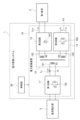
- FIG. 1 is a block diagram showing a power conversion system 1 including a power conversion device 10 according to the first embodiment, and peripheral devices 2 and 3 connected to the power conversion device 10.
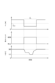
- FIG. 2 is a graph showing the relationship between the current IL1 flowing through the first coil 121 and the voltage V3 converted by the second switch QQ.
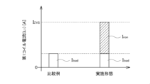
- FIG. 3 is a graph showing the current IL1 flowing through the first coil 121 when there is no reactive current Inon (comparative example) and when there is a reactive current Inon (embodiment).
- FIG. 4 is a circuit diagram showing an example of a detailed circuit configuration of the power conversion device 10 of FIG. FIG.
- FIG. 5 is a timing chart showing an example of a switching pattern of the first switch elements S1 to S4 and the second switch elements Q1 to Q4 in FIG.
- FIG. 6 is a graph showing the relationship between the phase difference ⁇ 31 between the first switch SS and the second switch QQ and the voltage value V3 converted by the second switch QQ.
- FIG. 7 is a graph showing an example of changes over time in the power value P1in input to the first circuit, the activation state of the second switch QQ, and the voltage V3 converted by the third circuit 14.
- FIG. FIG. 8 is a graph showing another example of the change over time in the power value P1in input to the first circuit, the activation state of the second switch QQ, and the voltage V3 converted by the third circuit 14.
- FIG. FIG. 8 is a graph showing another example of the change over time in the power value P1in input to the first circuit, the activation state of the second switch QQ, and the voltage V3 converted by the third circuit 14.
- FIG. 9 is a circuit diagram showing an example of a detailed circuit configuration of the power conversion device 10 of FIG. 1 according to the second embodiment.
- FIG. 10 is a graph showing another example of the change over time in the power value P1in input to the first circuit, the activation state of the second switch QQ, and the voltage V3 converted by the third circuit 14.
- FIG. 11 is a circuit diagram showing an example of a detailed circuit configuration of the power conversion device 10 of FIG. 1 according to the third embodiment.
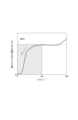
- FIG. 12 is a graph illustrating a large reactive current Z over that exceeds a current I ZVS required for soft switching.
- FIG. 13 is a flowchart showing an example of a control method for the power conversion device 10 according to the third embodiment.
- FIG. 10 is a graph showing another example of the change over time in the power value P1in input to the first circuit, the activation state of the second switch QQ, and the voltage V3 converted by the third circuit 14.
- FIG. 11 is a circuit diagram showing an example of a detailed circuit configuration
- FIG. 14 is a graph showing an example of changes over time in the parameters (power P 1in , start-up state of the second switch, current I L1 , and voltage V3) of the power conversion device 10 in the control method shown in FIG.
- FIG. 15 is a flowchart showing another example of the control method for the power conversion device 10 according to the third embodiment.
- FIG. 16 is a graph showing an example of changes over time in the parameters (power P 1in , start-up state of the second switch, current I L1 , and switching frequency F) of the power conversion device 10 in the control method shown in FIG.
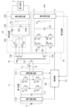
- the power conversion system 1 includes a power conversion device 10 having one input and two outputs, and a control unit 20 that controls the power conversion device 10.
- the power conversion device 10 includes a first circuit 11, a transformer 12, a second circuit 13, and a third circuit 14.
- the first circuit 11 includes a first switch SS that converts input power.
- the transformer 12 includes a first coil 121 to which the power converted by the first circuit 11 is input, a second coil 122 that converts and outputs the voltage input to the first coil 121, and a third coil 123 that converts and outputs the voltage input to the first coil 121.
- the second circuit 13 includes a rectifier circuit UU that converts the power output from the second coil 122.
- the third circuit 14 has a second switch QQ that converts the power output from the third coil 123 .
- the control unit 20 controls the second switch QQ as shown in formula (1) so that the voltage value V3 converted by the second switch QQ becomes equal to or less than the voltage value V1 input to the first circuit multiplied by the ratio (N3/N1) of the number of turns N3 of the third coil 123 to the number of turns N1 of the first coil 121.
- N3/N1 the ratio of the number of turns N3 of the third coil 123 to the number of turns N1 of the first coil 121.
- the soft switching (ZVS) of the first switch SS fails.
- the second switch QQ By controlling the second switch QQ so that the voltage V3 converted by the second switch QQ is reduced, a reactive current Inon is generated in the first coil 121 of the transformer 12. This increases the current I L1 flowing through the first coil 121.
- the power P1in input to the first circuit 11 also increases, so that the soft switching of the first switch SS can be realized.
- the soft switching of the first circuit 11 is possible by injecting the reactive current Inon .
- no load and light load are collectively referred to as light load.
- the first circuit 11 converts the DC power output from the DC voltage source 2 into AC power and outputs it to the first coil 121.
- the transformer 12 converts the input voltage to the first coil 121 into the output voltage of the second coil 122 according to the winding ratio (N2/N1) between the first coil 121 and the second coil 122.
- the transformer 12 converts the input voltage to the first coil 121 into the output voltage of the third coil 123 according to the winding ratio (N3/N1) between the first coil 121 and the third coil 123.
- the second circuit 13 converts the AC power output from the second coil 122 into DC power using the rectifier circuit UU and outputs it to the first load 3.
- the third circuit 14 converts the AC power output from the third coil 123 into DC power using the second switch QQ and outputs it.
- the first circuit 11 converts DC power into AC power by operating the first switch SS.
- the third circuit 14 converts AC power into DC power by operating the second switch.
- the third circuit 14 may have any circuit configuration as long as it is a switch-type power conversion circuit.
- the second circuit 13 may be a rectifier circuit UU using a diode or the like.
- a resonant coil 15 may be connected in series between the first circuit 11 and the first coil 121.
- the current I L1 flowing through the first coil 121 includes a current I load (hereinafter, may be referred to as a "load current I load ”) supplied to the first load 3.
- a current I load hereinafter, may be referred to as a "load current I load ” supplied to the first load 3.
- no load is connected to the output side of the third circuit 14.
- the voltage V3 converted by the second switch QQ drops, a reactive current I non is generated in the first coil 121 of the transformer 12.
- the current I L1 flowing through the first coil 121 is a value obtained by superimposing the reactive current I non on the load current I load .
- the lower the voltage V3 converted by the second switch QQ the greater the reactive current I non increases.
- the voltage V3 converted by the second switch QQ can be changed in the range of 0V to 360V by controlling the second switch QQ. 360V is an example of a voltage output from the DC voltage source 2.
- the control unit 20 controls the second switch QQ so that the voltage value V3 converted by the second switch QQ satisfies the condition shown in formula (1).
- the voltage value V3 becomes smaller than 360 V, so that a reactive current I non is generated and the current IL1 flowing through the first coil 121 increases.
- the power conversion device 10 or the power conversion system 1 can be mounted on an electric vehicle.
- the DC voltage source 2 can be a driving power source or a high-power battery for driving the electric vehicle.
- the first circuit 11, the transformer 12, and the second circuit 13 operate as an isolated DC-DC converter.
- the first circuit 11, the transformer 12, and the second circuit 13 step down the high voltage (e.g., 360 V) of the high-power battery to a low voltage (e.g., 14 V) and supply power to an on-vehicle auxiliary device (an example of a first load 3).
- the on-vehicle auxiliary device 3a includes a navigation device, a power window, brakes, wipers, headlights, and a door lock.
- the first load 3 may be an auxiliary device battery (14 V battery) for supplying power to the on-vehicle auxiliary device instead of the on-vehicle auxiliary device.
- the third circuit 14 can be used as a means for improving the efficiency of the isolated DC-DC converter composed of the first circuit 11, the transformer 12, and the second circuit 13, as described above.
- the second switch QQ can be used as a means for supplying a desired voltage to the load.
- loads connected to the output side of the third circuit 14 include power steering.
- the voltage applied can be controlled to, for example, 48 V by the second switch QQ.
- the second switch QQ when a load is connected to the output side of the third circuit 14, the second switch QQ is used as a means for applying a desired voltage to the load, and when no load is connected to the output side of the third circuit 14 (or when the load does not generate power consumption), the second switch QQ can be used as a means for improving the efficiency of the isolated DC-DC converter.
- the control unit 20 can be placed outside the electric vehicle by performing road-to-road communication with the power conversion device 10.
- the control unit 20 may be mounted on the electric vehicle and communicate with the power conversion device 10 via a wire such as CAN (Controller Area Network) wiring.
- the control unit 20 can be realized using a microcomputer equipped with a CPU (Central Processing Unit), memory, and input/output units.
- a computer program (control program) for causing the microcomputer to function as the control unit 20 is installed in the microcomputer and executed. This causes the microcomputer to function as multiple information processing units equipped in the control unit 20.
- the control unit 20 may also serve as an electronic control unit (ECU) used for other control related to the vehicle.
- ECU electronice control unit
- the first circuit 11 has first switch elements S1 to S4 as an example of a first switch SS
- the third circuit 14 has second switch elements Q1 to Q4 as an example of a second switch QQ.
- the second circuit 13 has a rectifier circuit 133 using two diodes U1 and U2 as an example of a rectifier circuit UU.
- the first coil 121, the second coil 122, and the third coil 123 are magnetically coupled by a core (iron core) 124.
- Each of the first circuit 11 and the third circuit 14 has an H-bridge circuit with four switch elements.
- the first leg and the second leg are connected in parallel between the high-voltage line and the low-voltage line.
- the switch elements that make up the H-bridge circuit can be composed of semiconductor devices including, for example, an IGBT (insulated gate bipolar transistor) and a MOSFET (metal-oxide-semiconductor field-effect transistor). By applying an on signal or an off signal to the gate electrode of the MOSFET, the conductive state (on) and cut-off state (off) of the switch can be controlled.
- the first switch elements S1 and S2 are connected in series on the first leg of the first circuit 11, and the first switch elements S3 and S4 are connected in series on the second leg of the first circuit 11.
- One terminal of the resonant coil 15 is connected between the first switch elements S1 and S2, and one terminal of the first coil 121 is connected between the first switch elements S3 and S4.
- the other terminal of the resonant coil 15 and the other terminal of the first coil 121 are connected.
- the first circuit 11 may have a smoothing capacitor 111 connected in parallel to the first leg and the second leg.
- the first circuit 11 may have a power detection unit 112 arranged between the DC voltage source 2 and the first switch elements S1 to S4.
- the power detection unit 112 detects the power P 1in input to the first circuit 11 and transmits a signal indicating the power P 1in to the control unit 20.
- the circuit configuration of the power detection unit 112 is not limited, and any known technology may be used.
- the second switch elements Q1 and Q2 are connected in series on the first leg of the third circuit 14, and the second switch elements Q3 and Q4 are connected in series on the second leg of the second circuit 13.
- One terminal of the resonant coil 142 is connected between the second switch elements Q1 and Q2, and one terminal of the third coil 123 is connected between the second switch elements Q3 and Q4.
- the other terminal of the resonant coil 142 and the other terminal of the third coil 123 are connected.
- the third circuit 14 may have a smoothing capacitor 141 connected in parallel to the first leg and the second leg.
- the third circuit 14 may have a voltage detection unit 143 that detects the voltage V3 converted by the second switch elements Q1 to Q4.
- the voltage detection unit 143 transmits a signal indicating the detected voltage V3 to the control unit 20.
- the circuit configuration of the voltage detection unit 143 is not important, and any known technology may be used.
- the rectifier circuit 133 is a center tap type rectifier circuit using two diodes U1 and U2, but may be a bridge type rectifier circuit.
- the anodes of the diodes U1 and U2 are common, and the cathodes of the diodes U1 and U2 are connected to both terminals of the second coil 122.
- the rectifier circuit 133 outputs the potential of the anodes of the diodes U1 and U2 and the potential at the midpoint of the second coil 122.
- the center tap type rectifier circuit 133 forms a full wave rectifier circuit like the bridge type rectifier circuit, but the number of diodes can be reduced.
- the second circuit 13 may include a smoothing circuit 134 consisting of an inductance 1341 and a capacitor 1342 on the output side of the rectifier circuit 133.
- the second circuit 13 may have a voltage detection unit 135 arranged between the smoothing circuit 134 and the first load 3.
- the voltage detection unit 135 detects the voltage V2 converted by the rectifier circuit 133 and smoothed by the smoothing circuit 134, and transmits a signal indicating the detected voltage V2 to the control unit 20.
- the circuit configuration of the voltage detection unit 135 is not important, and any known technology may be used.
- the switching pattern is a waveform that is generated by a driver circuit (not shown) to generate an on/off signal for each switch and input to the gate electrode of the MOSFET.
- the switching pattern is controlled by the control unit 20.
- the first switch element S1 and the first switch element S2 on the first leg alternately turn on and off.
- the first switch element S1 is on
- the first switch element S2 is off
- the first switch element S1 is off
- the first switch element S2 is on
- the first switch element S3 and the first switch element S4 on the second leg alternately turn on and off. All of the first switch elements S1 to S4 turn on and off in the same cycle, and the proportion of times they are on in one cycle, i.e., the duty ratio, is 50%.
- the second switch elements Q1 and Q2 on the first leg alternately turn on and off.
- the second switch element Q1 is on
- the second switch element Q2 is off
- the second switch element Q1 is off
- the second switch element Q2 is on
- the second switch elements Q3 and Q4 on the second leg alternately turn on and off.
- the second switch elements Q1 to Q4 all turn on and off in the same cycle, and the proportion of on in one cycle, i.e., the duty ratio, is 50%.
- the cycle of the second switch elements Q1 to Q4 is the same as the cycle of the first switch elements S1 to S4.
- the control unit 20 controls the phase ⁇ 1 of the first switch SS and the phase difference ⁇ 31 between the first switch SS and the second switch QQ.
- the "phase ⁇ 1 of the first switch SS” is the phase difference between the phase of the on/off switching of the first switch element S1 and the first switch element S2 on the first leg and the phase of the on/off switching of the first switch element S3 and the first switch element S4 on the second leg.
- the "phase ⁇ 1 of the first switch SS” is the phase difference between the first leg and the second leg of the first circuit 11. Note that FIG.
- the phase difference between the phase of the fall (on ⁇ off) of the first switch element S1 and the phase of the rise (off ⁇ on) of the first switch element S2 and the phase of the fall (on ⁇ off) of the first switch element S4 and the rise (off ⁇ on) of the first switch element S3 is also the same "phase ⁇ 1".
- phase difference ⁇ 31 between the first switch SS and the second switch QQ is the phase difference between the phase of the on/off switching of the first switch element S1 and the phase of the on/off switching of the second switch element Q1.
- the first switch elements S1 to S4 and the second switch elements Q1 to Q4 have the same period and duty ratio. Therefore, the phase difference between the phase of the on/off switching of the first switch elements S2 to S4 and the phase of the on/off switching of the second switch elements Q2 to Q4 is also the same "phase difference ⁇ 31.”
- the control unit 20 controls the phase ⁇ 1 of the first switch SS to control the voltage V2 converted by the second circuit 13 to a constant voltage (e.g., 14 V).
- the control unit 20 controls the phase difference ⁇ 31 between the first switch SS and the second switch QQ to control the voltage V3 converted by the third circuit 14 to a desired value.
- the control unit 20 may control the phase difference ⁇ 31 so as to satisfy the condition shown in formula (1) based on the relationship between the phase difference ⁇ 31 and the voltage V3 shown in FIG. 6.
- the control unit 20 may also control the voltage V3 to 0V (zero volts) by setting the phase difference ⁇ 31 to zero.
- 0V includes a range from exactly 0V to near 0V, specifically up to a few percent of the voltage V1, for example up to about 10V.
- the method of controlling the voltage V3 converted by the third circuit 14 is not limited to the above-mentioned method.
- the second switch elements Q1 and Q2 can be synchronized with the first switch elements S1 and S2, and a phase difference can be provided only between the second switch elements Q3 and Q4 and the first switch elements S3 and S4, thereby controlling the amount of power received by the third circuit 14. This makes it possible to change the voltage V3 converted by the third circuit 14.
- the third circuit is equivalent to a rectifier circuit using the body diode (a diode provided in the case of an IGBT) included in the second switch QQ, so that the voltage (360V) input to the third circuit 14 is output as it is.
- the control unit 20 can reduce the switching loss of the third circuit 14 that occurs when the second switch QQ is operated.
- the control unit 20 activates the second switch QQ that has been inactive.
- the control unit 20 controls the phase difference ⁇ 31 with reference to the graph shown in FIG. 6 to reduce the voltage V3 converted by the second switch QQ to a value lower than 360 V.
- the reference value Th1 may be set by calculating a power value at which soft switching of the first switch SS is impossible from the specifications and circuit constants of the first switch elements S1 to S4.
- FIG. 8 another example of the change over time of the power value P1in input to the first circuit, the start-up state of the second switch QQ, and the voltage V3 converted by the third circuit 14 will be described.
- FIG. 7 when the second switch QQ is started and the voltage V3 converted by the second switch QQ is reduced to a finite value other than zero, a switching loss occurs in the second switch QQ. Therefore, as shown in FIG. 8, when the power value P1in input to the first circuit 11 is less than the reference value Th1 (light load LL), the control unit 20 starts the second switch QQ and reduces the voltage V3 converted by the second switch QQ to 0V.
- Th1 light load LL
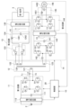
- Fig. 9 corresponds to an example of a detailed circuit configuration of the power conversion device 10 in Fig. 1.
- the example shown in Fig. 9 is different from the example in Fig. 4 in that the third circuit 14 further includes a DCAC inverter 144 to which power converted by the second switch QQ (second switch elements Q1 to Q4) is input.
- the other configurations in Fig. 9 except for the third circuit 14 are the same as those in Fig. 4, and will not be described again.
- the DCAC inverter 144 has an H-bridge circuit with four third switch elements Y1 to Y4.
- the first leg and the second leg are connected in parallel between the high-voltage line and the low-voltage line.
- the third switch elements Y1 to Y4 that make up the H-bridge circuit can be composed of semiconductor devices including, for example, IGBTs and MOSFETs.
- the conductive state (on) and cut-off state (off) of the switches can be controlled by applying an on signal or an off signal to the gate electrode of the MOSFET.
- the third switch elements Y1 and Y2 are connected in series on the first leg of the DCAC inverter 144, and the third switch elements Y3 and Y4 are connected in series on the second leg of the DCAC inverter 144. Both terminals of the voltage detection unit 143 are connected between the third switch elements Y1 and Y2 and between the third switch elements Y3 and Y4, respectively.
- the third circuit 14 may include a smoothing circuit 145 that smoothes the AC power converted by the DCAC inverter 144.
- the smoothing circuit 145 has an inductance 1451 and a capacitor 1452.
- the AC voltage converted from the DC voltage (voltage V3) by the DCAC inverter 144 is output to the outlet 146 via the smoothing circuit 145.
- the DCAC inverter 144 converts the AC voltage to, for example, a commercial power supply voltage (AC 100V) in Japan and outputs it.
- the power conversion device 10 or power conversion system 1 according to the second embodiment can be mounted on an electric vehicle.
- the second circuit 13 can supply power to the on-board auxiliary equipment 3a while supplying power to electrical appliances inside and outside the vehicle.
- the DCDC converter for the on-board auxiliary equipment which is an example of the first load 3, and the DCAC inverter for the outlet 146, which were mounted separately on the electric vehicle, can be integrated.
- the input side circuit (first circuit 11) and the transformer 12 can be integrated to individually control the power output from the two output side circuits (second circuit 13, third circuit 14).
- the control unit 20 controls the second switch QQ (second switch elements Q1 to Q4) so that the voltage value V3 converted by the second switch QQ (second switch elements Q1 to Q4) is equal to or less than the value obtained by multiplying the voltage value V1 input to the first circuit 11 by the ratio (N3/N1) of the number of turns N3 of the third coil 123 to the number of turns N1 of the first coil 121, as shown in formula (1).
- N3/N1 the ratio
- the third circuit 14 cannot output the desired power or voltage to the load (electrical appliance) connected to the output of the third circuit 14.
- the third circuit 14 has a DCAC inverter 144 in the rear stage of the second switch elements Q1 to Q4, even if the voltage V3 converted by the second switch elements Q1 to Q4 is somewhat low, the desired power or voltage can be output to the load (electrical appliance) to which the power converted by the DCAC inverter 144 is supplied by controlling the DCAC inverter 144 in the rear stage. Therefore, the existence of the third circuit 14 makes it possible to integrate an outlet DCAC inverter into an insulated DC-DC converter for on-board accessories, outputting AC 100V while simultaneously improving the efficiency of the DC-DC converter.
- the control unit 20 sets the lower limit of the voltage V3 converted by the second switch QQ (second switch elements Q1 to Q4) to the maximum value (e.g., 141 V) of the AC voltage converted by the DCAC inverter. If the voltage V3 converted by the second switch QQ is significantly reduced when the DCAC inverter 144 is outputting an AC voltage, the DCAC inverter 144 cannot output a desired AC voltage.
- the lower limit of the voltage V3 converted by the second switch QQ is set to the maximum value of the AC voltage converted by the DCAC inverter.
- the maximum value of the AC voltage is 141 V. This allows the DCAC inverter 144 to output a desired AC voltage. This is an effective control method particularly when the DCAC inverter 144 is supplying AC power to a load connected to the outlet 146.
- the control unit 20 may control the second switch QQ (second switches Q1 to Q4) so that the voltage value V3 converted by the second switch QQ becomes 0 V, as shown in FIG. 8.
- the voltage V3 converted by the second switch QQ is controlled to 0 V or close to 0 V, thereby reducing the switching loss of the third circuit 14 that occurs when the second switch QQ is operated.
- the control unit 20 may start the second switch QQ (the second switches Q1 to Q4) without pausing it.
- the body diode of the second switch QQ operates as a rectifier, so that the voltage (360V) input to the third circuit 14 is supplied to the DCAC inverter 144 as is, but the control unit 20 may control the second switches Q1 to Q4 to adjust the power and voltage supplied to the DCAC inverter 144.
- Fig. 11 corresponds to an example of a detailed circuit configuration of the power conversion device 10 in Fig. 1.
- the example shown in Fig. 11 differs from the example in Fig. 4 in that the first circuit 11 further includes a current detection unit 113 that detects a current IL1 flowing through a first coil 121 of the transformer 12.
- the other configurations in Fig. 11 except for the first circuit 11 are the same as those in Fig. 4, and will not be described again.
- the current detection unit 113 detects the current I L1 converted by the first switch elements S1 to S4 and output from the first circuit 11.
- the current detection unit 113 transmits a signal indicating the detected current I L1 to the control unit 20.
- the circuit configuration of the voltage detection unit 135 is not important, and any known technology may be used.
- the control unit 20 changes the voltage V3 converted by the second switch QQ (second switch elements Q1 to Q4) according to the current value I L1 flowing through the first coil 121 of the transformer 12.
- This allows the minimum reactive current I non required for soft switching to be generated, minimizing the conduction loss of the first switch SS and the second switch QQ.
- the load current I load in Fig. 12 decreases, the reactive current I non required for soft switching increases, and the voltage V3 required for soft switching also decreases. In this way, it is possible to deal with the case where the value of the reactive current I non required for soft switching changes due to a change in the load (load current I load ).
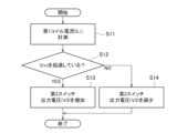
- the voltage V3 converted by the second switch QQ may be controlled according to the flowchart shown in FIG. 13.
- the current detection unit 113 detects the current I L1 flowing through the first coil 121 of the transformer 12, and transmits a signal indicating the current I L1 to the control unit 20.
- the control unit 20 judges whether the current I L1 exceeds the current I ZVS required for soft switching. If it exceeds (YES in step S12), the soft switching has been successful and there is no need to further increase the reactive current I non . In this case, the control unit 20 increases the voltage V3. If it does not exceed (NO in step S12), the soft switching has not been achieved and there is no need to further increase the reactive current I non .
- control unit 20 decreases the voltage V3.
- the control unit 20 repeatedly executes steps S11 to S14 at a predetermined control period, thereby making it possible for the voltage V3 converted by the second switching elements Q1 to Q4 to converge to the voltage V ZVS in Fig. 12. Therefore, the control unit 20 can generate the minimum reactive current I non necessary to realize soft switching.
- the control method of Fig. 13 can optimize the reactive current Inon . That is, when the power P1in is small under light load (LL), the control unit 20 activates the second switch QQ and optimizes the voltage V3 converted by the second switch QQ so that the current I L1 flowing through the first coil 121 coincides with the current I ZVS . After that, when the power P1in input to the first circuit 11 is further decreased (3L) compared to the light load (LL), the current I L1 flowing through the first coil 121 temporarily decreases. However, the control unit 20 reduces the voltage V3 converted by the second switch QQ to increase the reactive current Inon .
- the switching frequency F of the first switch SS and the second switch QQ may be increased instead of the voltage V3 converted by the second switch QQ. That is, when the power value P.sub.1in input to the first circuit 11 is less than the reference value Th1, the control unit 20 may change the switching frequency F of the first switch SS and the second switch QQ according to the current value IL1 flowing through the first coil 121 of the transformer 12.
- the relationship between the reactive current I.sub.non and the switching frequency F is shown in Equation (2). The higher the switching frequency F, the more the reactive current I.sub.non decreases.
- the second switch QQ can keep the voltage V3 at 0V while suppressing the reactive current to a necessary minimum, making it possible to achieve soft switching of the first switch SS while significantly reducing the switching loss of the second switch QQ.
- step S24 the control unit 20 increases the switching frequency F to increase the reactive current I non .
- the control unit 20 repeatedly executes steps S11, S12, S23, and S24 in a predetermined control period, and thereby the control unit 20 can generate the minimum reactive current I non required to realize soft switching.
- the control unit 20 changes the switching frequency F of the first switch SS and the second switch QQ while measuring the current value IL1 on the primary side of the transformer 12, thereby generating the minimum reactive current IZVS required for soft switching on the primary side (input side) of the transformer 12, thereby minimizing switching loss.
- the control method of Fig. 15 can optimize the reactive current Inon . That is, when the power P1in is small under light load (LL), the control unit 20 activates the second switch QQ and optimizes the switching frequency F of the first switch SS and the second switch QQ so that the current I L1 flowing through the first coil 121 coincides with the current I ZVS . After that, when the power P1in input to the first circuit 11 is further decreased (3L) compared to the light load (LL), the current I L1 flowing through the first coil 121 temporarily decreases. The control unit 20 reduces the switching frequency F of the first switch SS and the second switch QQ to increase the reactive current Inon .
- the control unit 20 may simultaneously execute the control method shown in Fig. 13 and the control method shown in Fig. 15.
Landscapes
- Engineering & Computer Science (AREA)
- Power Engineering (AREA)
- Dc-Dc Converters (AREA)
Priority Applications (2)
| Application Number | Priority Date | Filing Date | Title |
|---|---|---|---|
| JP2025523747A JPWO2024247111A1 (https=) | 2023-05-30 | 2023-05-30 | |
| PCT/JP2023/020103 WO2024247111A1 (ja) | 2023-05-30 | 2023-05-30 | 電力変換装置の制御方法及び電力変換システム |
Applications Claiming Priority (1)
| Application Number | Priority Date | Filing Date | Title |
|---|---|---|---|
| PCT/JP2023/020103 WO2024247111A1 (ja) | 2023-05-30 | 2023-05-30 | 電力変換装置の制御方法及び電力変換システム |
Publications (1)
| Publication Number | Publication Date |
|---|---|
| WO2024247111A1 true WO2024247111A1 (ja) | 2024-12-05 |
Family
ID=93657160
Family Applications (1)
| Application Number | Title | Priority Date | Filing Date |
|---|---|---|---|
| PCT/JP2023/020103 Ceased WO2024247111A1 (ja) | 2023-05-30 | 2023-05-30 | 電力変換装置の制御方法及び電力変換システム |
Country Status (2)
| Country | Link |
|---|---|
| JP (1) | JPWO2024247111A1 (https=) |
| WO (1) | WO2024247111A1 (https=) |
Citations (3)
| Publication number | Priority date | Publication date | Assignee | Title |
|---|---|---|---|---|
| JP2005151608A (ja) * | 2003-11-11 | 2005-06-09 | Hitachi Ltd | 共振型コンバータ及びその制御方法 |
| WO2019199964A1 (en) * | 2018-04-10 | 2019-10-17 | University Of Maryland College Park | Vehicle on-board charger for bi-directional charging of low/high voltage batteries |
| JP6996661B1 (ja) * | 2020-02-21 | 2022-01-17 | 住友電気工業株式会社 | 電力変換装置、それを含む車両及び制御方法 |
-
2023
- 2023-05-30 JP JP2025523747A patent/JPWO2024247111A1/ja active Pending
- 2023-05-30 WO PCT/JP2023/020103 patent/WO2024247111A1/ja not_active Ceased
Patent Citations (3)
| Publication number | Priority date | Publication date | Assignee | Title |
|---|---|---|---|---|
| JP2005151608A (ja) * | 2003-11-11 | 2005-06-09 | Hitachi Ltd | 共振型コンバータ及びその制御方法 |
| WO2019199964A1 (en) * | 2018-04-10 | 2019-10-17 | University Of Maryland College Park | Vehicle on-board charger for bi-directional charging of low/high voltage batteries |
| JP6996661B1 (ja) * | 2020-02-21 | 2022-01-17 | 住友電気工業株式会社 | 電力変換装置、それを含む車両及び制御方法 |
Also Published As
| Publication number | Publication date |
|---|---|
| JPWO2024247111A1 (https=) | 2024-12-05 |
Similar Documents
| Publication | Publication Date | Title |
|---|---|---|
| WO2015004948A1 (ja) | 放電制御装置 | |
| CN103227610B (zh) | 电机控制电路和汽车 | |
| CN115836469B (zh) | 电力转换装置及电力系统 | |
| JP6771156B2 (ja) | 電力変換装置 | |
| JP2016100989A (ja) | 直流変換装置 | |
| US8630104B2 (en) | Switching power supply and display device provided the same | |
| JP2023144659A (ja) | 電力供給システム | |
| JP2019083658A (ja) | 電力変換装置 | |
| JP2022069834A (ja) | 電源制御装置 | |
| JP2010518806A (ja) | インバータ | |
| CN110546874B (zh) | 电力转换系统 | |
| KR20220045024A (ko) | 플러그인 전기 자동차용 충전기 | |
| JP2019149867A (ja) | 電力変換装置及び電力変換システム | |
| CN109756136B (zh) | 开关电源 | |
| KR20230112174A (ko) | 고효율로 동작하는 전기 자동차용 급속충전기 및 이를 동작시키는 방법 | |
| WO2024247111A1 (ja) | 電力変換装置の制御方法及び電力変換システム | |
| JP6992014B2 (ja) | Dc-dc電圧コンバータ回路を制御する制御システム | |
| KR20210099813A (ko) | 전기자동차용 고전압 dc-dc 컨버터 | |
| JP7315105B2 (ja) | 電源回路 | |
| JP7035407B2 (ja) | 電力変換装置 | |
| WO2024247096A1 (ja) | 電力変換装置の制御方法及び電力変換システム | |
| JP2024171540A (ja) | 電力変換装置、その制御方法、及び電力変換システム | |
| US9660531B1 (en) | System and method for improving efficiency for quasi-square wave power converters | |
| CN113632380A (zh) | 电力电子设备和用于向功率半导体开关的驱动电路供应电压的方法 | |
| KR102694018B1 (ko) | 스위치 구동 전원부를 포함하는 전기차를 위한 급속 충전 전원 장치 |
Legal Events
| Date | Code | Title | Description |
|---|---|---|---|
| 121 | Ep: the epo has been informed by wipo that ep was designated in this application |
Ref document number: 23939590 Country of ref document: EP Kind code of ref document: A1 |
|
| ENP | Entry into the national phase |
Ref document number: 2025523747 Country of ref document: JP Kind code of ref document: A |
|
| NENP | Non-entry into the national phase |
Ref country code: DE |