WO2024225088A1 - 電力変換装置 - Google Patents
電力変換装置 Download PDFInfo
- Publication number
- WO2024225088A1 WO2024225088A1 PCT/JP2024/014914 JP2024014914W WO2024225088A1 WO 2024225088 A1 WO2024225088 A1 WO 2024225088A1 JP 2024014914 W JP2024014914 W JP 2024014914W WO 2024225088 A1 WO2024225088 A1 WO 2024225088A1
- Authority
- WO
- WIPO (PCT)
- Prior art keywords
- switching element
- switching
- power conversion
- terminal
- conversion device
- Prior art date
- Legal status (The legal status is an assumption and is not a legal conclusion. Google has not performed a legal analysis and makes no representation as to the accuracy of the status listed.)
- Ceased
Links
Images


Classifications
-
- H—ELECTRICITY
- H02—GENERATION; CONVERSION OR DISTRIBUTION OF ELECTRIC POWER
- H02M—APPARATUS FOR CONVERSION BETWEEN AC AND AC, BETWEEN AC AND DC, OR BETWEEN DC AND DC, AND FOR USE WITH MAINS OR SIMILAR POWER SUPPLY SYSTEMS; CONVERSION OF DC OR AC INPUT POWER INTO SURGE OUTPUT POWER; CONTROL OR REGULATION THEREOF
- H02M1/00—Details of apparatus for conversion
- H02M1/0048—Circuits or arrangements for reducing losses
- H02M1/0054—Transistor switching losses
- H02M1/0058—Transistor switching losses by employing soft switching techniques, i.e. commutation of transistors when applied voltage is zero or when current flow is zero
-
- H—ELECTRICITY
- H02—GENERATION; CONVERSION OR DISTRIBUTION OF ELECTRIC POWER
- H02M—APPARATUS FOR CONVERSION BETWEEN AC AND AC, BETWEEN AC AND DC, OR BETWEEN DC AND DC, AND FOR USE WITH MAINS OR SIMILAR POWER SUPPLY SYSTEMS; CONVERSION OF DC OR AC INPUT POWER INTO SURGE OUTPUT POWER; CONTROL OR REGULATION THEREOF
- H02M7/00—Conversion of AC power input into DC power output; Conversion of DC power input into AC power output
- H02M7/42—Conversion of DC power input into AC power output without possibility of reversal
- H02M7/44—Conversion of DC power input into AC power output without possibility of reversal by static converters
- H02M7/48—Conversion of DC power input into AC power output without possibility of reversal by static converters using discharge tubes with control electrode or semiconductor devices with control electrode
- H02M7/4815—Resonant converters
-
- H—ELECTRICITY
- H02—GENERATION; CONVERSION OR DISTRIBUTION OF ELECTRIC POWER
- H02M—APPARATUS FOR CONVERSION BETWEEN AC AND AC, BETWEEN AC AND DC, OR BETWEEN DC AND DC, AND FOR USE WITH MAINS OR SIMILAR POWER SUPPLY SYSTEMS; CONVERSION OF DC OR AC INPUT POWER INTO SURGE OUTPUT POWER; CONTROL OR REGULATION THEREOF
- H02M7/00—Conversion of AC power input into DC power output; Conversion of DC power input into AC power output
- H02M7/42—Conversion of DC power input into AC power output without possibility of reversal
- H02M7/44—Conversion of DC power input into AC power output without possibility of reversal by static converters
- H02M7/48—Conversion of DC power input into AC power output without possibility of reversal by static converters using discharge tubes with control electrode or semiconductor devices with control electrode
- H02M7/53—Conversion of DC power input into AC power output without possibility of reversal by static converters using discharge tubes with control electrode or semiconductor devices with control electrode using devices of a triode or transistor type requiring continuous application of a control signal
- H02M7/537—Conversion of DC power input into AC power output without possibility of reversal by static converters using discharge tubes with control electrode or semiconductor devices with control electrode using devices of a triode or transistor type requiring continuous application of a control signal using semiconductor devices only, e.g. single switched pulse inverters
- H02M7/5387—Conversion of DC power input into AC power output without possibility of reversal by static converters using discharge tubes with control electrode or semiconductor devices with control electrode using devices of a triode or transistor type requiring continuous application of a control signal using semiconductor devices only, e.g. single switched pulse inverters in a bridge configuration
- H02M7/53871—Conversion of DC power input into AC power output without possibility of reversal by static converters using discharge tubes with control electrode or semiconductor devices with control electrode using devices of a triode or transistor type requiring continuous application of a control signal using semiconductor devices only, e.g. single switched pulse inverters in a bridge configuration with automatic control of output voltage or current
-
- H—ELECTRICITY
- H02—GENERATION; CONVERSION OR DISTRIBUTION OF ELECTRIC POWER
- H02M—APPARATUS FOR CONVERSION BETWEEN AC AND AC, BETWEEN AC AND DC, OR BETWEEN DC AND DC, AND FOR USE WITH MAINS OR SIMILAR POWER SUPPLY SYSTEMS; CONVERSION OF DC OR AC INPUT POWER INTO SURGE OUTPUT POWER; CONTROL OR REGULATION THEREOF
- H02M1/00—Details of apparatus for conversion
- H02M1/38—Means for preventing simultaneous conduction of switches
-
- Y—GENERAL TAGGING OF NEW TECHNOLOGICAL DEVELOPMENTS; GENERAL TAGGING OF CROSS-SECTIONAL TECHNOLOGIES SPANNING OVER SEVERAL SECTIONS OF THE IPC; TECHNICAL SUBJECTS COVERED BY FORMER USPC CROSS-REFERENCE ART COLLECTIONS [XRACs] AND DIGESTS
- Y02—TECHNOLOGIES OR APPLICATIONS FOR MITIGATION OR ADAPTATION AGAINST CLIMATE CHANGE
- Y02B—CLIMATE CHANGE MITIGATION TECHNOLOGIES RELATED TO BUILDINGS, e.g. HOUSING, HOUSE APPLIANCES OR RELATED END-USER APPLICATIONS
- Y02B70/00—Technologies for an efficient end-user side electric power management and consumption
- Y02B70/10—Technologies improving the efficiency by using switched-mode power supplies [SMPS], i.e. efficient power electronics conversion e.g. power factor correction or reduction of losses in power supplies or efficient standby modes
Definitions
- This disclosure relates to a power conversion device, and more specifically, to a power conversion device capable of converting DC power to AC power.
- Patent document 1 discloses a power conversion system.
- the power conversion system (power conversion device) disclosed in Patent Document 1 includes a switching means having a pair of main switching elements (first switching element and second switching element) connected in series with each other, diodes (first diode and second diode) connected in anti-parallel to each main switching element, an auxiliary circuit for performing soft switching of each main switching element, and a controller.
- the auxiliary circuit includes two capacitors, a coil (resonant inductor), and an auxiliary switch.
- the controller generates a control signal for PWM control of each main switching element and outputs it to the gate of each main switching element.
- the controller also generates a control signal for controlling the on/off of the auxiliary switch and outputs it to the gate of the auxiliary switch.
- radiated noise may increase.
- the purpose of this disclosure is to provide a power conversion device that can reduce radiated noise.
- a power conversion device includes a first DC terminal and a second DC terminal, a power conversion circuit, a switch, a resonant capacitor, a resonant inductor, a regenerative capacitor, and a control device.
- the power conversion circuit has a switching circuit.
- the switching circuit includes a first switching element and a second switching element connected in series with each other, a first diode connected in anti-parallel to the first switching element, and a second diode connected in anti-parallel to the second switching element.
- the first switching element is connected to the first DC terminal
- the second switching element is connected to the second DC terminal.
- the switch has a first end and a second end.
- the first end of the switch is connected to a connection point between the first switching element and the second switching element.
- the resonant capacitor is connected between the first end and the second DC terminal of the switch.
- the resonant inductor is connected to the second end of the switch.
- the regenerative capacitor is connected between the resonant inductor and the second DC terminal.
- the control device controls the first switching element, the second switching element, and the switch.
- the switch includes a third switching element and a fourth switching element. When the third switching element is in an on state, a current flows from the resonant inductor side. When the fourth switching element is in an on state, a current flows in the opposite direction to that of the third switching element.
- the control device provides a control signal whose potential changes between a high level and a low level to each of the first switching element, the second switching element, the third switching element, and the fourth switching element.
- the control device sets a dead time period between a high level period of the control signal to the first switching element and a high level period of the control signal to the second switching element.
- the control device overlaps at least a part of the high level period of the control signal to the third switching element with the dead time period.
- the control device causes the third switching element to maintain a state immediately before the ringing period during a ringing period in which ringing occurs in the voltage across the third switching element.
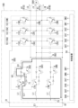
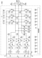
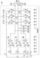
- FIG. 1 is a circuit diagram of a system including a power conversion device according to a first embodiment.
- FIG. 2 is a diagram showing a time change in duty and a time change in load current corresponding to voltage commands for each of three phases in an AC load connected to a plurality of AC terminals of the power conversion device according to the above embodiment.
- FIG. 3 is an explanatory diagram of the basic operation of the power conversion device.
- FIG. 4 is an explanatory diagram of the basic operation of the power conversion device.
- FIG. 5 is an explanatory diagram of the basic operation of the power conversion device.
- FIG. 6 is a diagram illustrating the operation of the power conversion device.
- FIG. 7 is a diagram illustrating the operation of the power conversion device.
- FIG. 8 is a timing chart for explaining the operation of the power conversion device.
- FIG. 9 is a timing chart for explaining the operation of the comparative example of the power conversion device.
- FIG. 10 is a characteristic diagram showing measurement results of radiation noise of the embodiment and the comparative example of the power conversion device of the same.
- FIG. 11 is a circuit diagram of a system including a power conversion device according to the second embodiment.
- FIG. 12 is a circuit diagram of a system including a power conversion device according to the third embodiment.
- FIG. 13 is a circuit diagram of a system including a power conversion device according to the fourth embodiment.
- FIG. 14 is a circuit diagram of a system including a power conversion device according to the fifth embodiment.
- FIG. 15 is a timing chart for explaining the operation of the power conversion device.
- FIG. 16 is a circuit diagram of a system including a power conversion device according to the sixth embodiment.
- FIG. 17 is a circuit diagram of a system including a power conversion device according to the seventh embodiment.
- FIG. 18 is a circuit diagram of a system including a power conversion device according to
- the power conversion device 100 includes a first DC terminal 31, a second DC terminal 32, and a plurality of (three in the example of FIG. 1) AC terminals 41.
- a DC power source E1 is connected between the first DC terminal 31 and the second DC terminal 32, and an AC load RA1 is connected to the plurality of AC terminals 41.
- the AC load RA1 is, for example, a three-phase motor.
- the power conversion device 100 converts the DC output from the DC power source E1 into AC power and outputs it to the AC load RA1.
- the DC power source E1 includes, for example, a solar cell or a fuel cell.
- the DC power source E1 may include a DC-DC converter.
- the AC power is, for example, three-phase AC power having a U phase, a V phase, and a W phase.
- the power conversion device 100 includes a power conversion circuit 11, a plurality of switches 8 (three in the example of FIG. 1), a plurality of resonant capacitors 9 (three in the example of FIG. 1), a regenerative capacitor 15, a plurality of resonant inductors L1 (three in the example of FIG. 1), and a control device 50.
- Each of the plurality of switches 8 is, for example, a bidirectional switch.
- the power conversion circuit 11 has a plurality of first switching elements 1 (three in the example of FIG. 1) and a plurality of second switching elements 2 (three in the example of FIG. 1).
- a plurality of switching circuits 10 (three in the example of FIG. 1) in which a plurality of first switching elements 1 and a plurality of second switching elements 2 are connected in series in a one-to-one relationship are connected in parallel to each other.
- the plurality of first switching elements 1 are connected to a first DC terminal 31, and the plurality of second switching elements 2 are connected to a second DC terminal 32.
- the multiple AC terminals 41 correspond one-to-one to the multiple switching circuits 10. Each of the multiple AC terminals 41 is connected to the connection point 3 of the first switching element 1 and the second switching element 2 in the corresponding switching circuit 10 among the multiple switching circuits 10.
- the multiple switches 8 correspond one-to-one to the multiple switching circuits 10.
- Each of the multiple switches 8 has a first end 81 and a second end 82.
- the first end 81 of each of the multiple switches 8 is connected to the connection point 3 of the first switching element 1 and the second switching element 2 in the corresponding switching circuit 10 among the multiple switching circuits 10.
- the multiple resonant capacitors 9 correspond one-to-one to the multiple switches 8. Each of the multiple resonant capacitors 9 is connected between the first end 81 and the second DC terminal 32 of a corresponding switch 8 among the multiple switches 8.
- Each of the multiple resonant inductors L1 has a third end and a fourth end.
- the fourth end is connected to the regenerative capacitor 15.
- the third end is connected to the second end 82 of a corresponding one of the multiple switches 8.
- the regenerative capacitor 15 has a fifth end 153 and a sixth end 154.
- the fifth end 153 is connected to the second DC terminal 32
- the sixth end 154 is connected to the fourth ends of the multiple resonant inductors L1.
- the control device 50 controls the multiple first switching elements 1, the multiple second switching elements 2, and the multiple switches 8.
- the switching circuits 10 corresponding to the U-phase, V-phase, and W-phase of the multiple switching circuits 10 may be referred to as a switching circuit 10U, a switching circuit 10V, and a switching circuit 10W, respectively.
- the first switching element 1 and the second switching element 2 of the switching circuit 10U may be referred to as a first switching element 1U and a second switching element 2U.
- the first switching element 1 and the second switching element 2 of the switching circuit 10V may be referred to as a first switching element 1V and a second switching element 2V.
- the first switching element 1 and the second switching element 2 of the switching circuit 10W may be referred to as a first switching element 1W and a second switching element 2W.
- the connection point 3 between the first switching element 1U and the second switching element 2U may be referred to as the connection point 3U
- the connection point 3 between the first switching element 1V and the second switching element 2V may be referred to as the connection point 3V
- the connection point 3 between the first switching element 1W and the second switching element 2W may be referred to as the connection point 3W.
- the AC terminal 41 connected to the connection point 3U may be referred to as the AC terminal 41U
- the AC terminal 41 connected to the connection point 3V may be referred to as the AC terminal 41V
- the AC terminal 41 connected to the connection point 3W may be referred to as the AC terminal 41W.
- the resonant capacitor 9 connected in parallel to the second switching element 2U may be referred to as the resonant capacitor 9U
- the resonant capacitor 9 connected in parallel to the second switching element 2V may be referred to as the resonant capacitor 9V
- the resonant capacitor 9 connected in parallel to the second switching element 2W may be referred to as the resonant capacitor 9W.
- switch 8U the switch 8 connected to connection point 3U
- switch 8V the switch 8 connected to connection point 3V
- switch 8W the switch 8 connected to connection point 3W
- the high-potential output terminal (positive electrode) of the DC power supply E1 is connected to the first DC terminal 31, and the low-potential output terminal (negative electrode) of the DC power supply E1 is connected to the second DC terminal 32.
- the U-phase terminal, V-phase terminal, and W-phase terminal of the AC load RA1 are connected to the three AC terminals 41U, 41V, and 41W, respectively.
- each of the multiple (three in the example of FIG. 1) first switching elements 1 and the multiple (three in the example of FIG. 1) second switching elements 2 has a control terminal, a first main terminal, and a second main terminal.
- the control terminals of the multiple first switching elements 1 and the multiple second switching elements 2 are connected to the control device 50.
- the first main terminal of the first switching element 1 is connected to the first DC terminal 31
- the second main terminal of the first switching element 1 is connected to the first main terminal of the second switching element 2
- the second main terminal of the second switching element 2 is connected to the second DC terminal 32.
- the first switching element 1 is a high-side switching element (P-side switching element), and the second switching element 2 is a low-side switching element (N-side switching element).
- Each of the multiple first switching elements 1 and the multiple second switching elements 2 is, for example, an IGBT (Insulated Gate Bipolar Transistor). Therefore, the control terminal, the first main terminal, and the second main terminal of each of the multiple first switching elements 1 and the multiple second switching elements 2 are the gate terminal, the collector terminal, and the emitter terminal, respectively.
- the power conversion circuit 11 further includes a plurality (three) of first diodes 4 connected in anti-parallel to a plurality (three) of first switching elements 1 in a one-to-one relationship, and a plurality (three) of second diodes 5 connected in anti-parallel to a plurality (three) of second switching elements 2 in a one-to-one relationship.
- the anode of the first diode 4 is connected to the second main terminal (emitter terminal) of the first switching element 1 corresponding to the first diode 4
- the cathode of the first diode 4 is connected to the first main terminal (collector terminal) of the first switching element 1 corresponding to the first diode 4.
- the anode of the second diode 5 is connected to the second main terminal (emitter terminal) of the second switching element 2 corresponding to the second diode 5, and the cathode of the second diode 5 is connected to the first main terminal (collector terminal) of the second switching element 2 corresponding to the second diode 5.
- connection point 3U between the first switching element 1U and the second switching element 2U is connected to, for example, the U-phase terminal of the AC load RA1 via the AC terminal 41U.
- connection point 3V between the first switching element 1V and the second switching element 2V is connected to, for example, the V-phase of the AC load RA1 via the AC terminal 41V.
- connection point 3W between the first switching element 1W and the second switching element 2W is connected to, for example, the W-phase of the AC load RA1 via the AC terminal 41W.
- the multiple resonant capacitors 9 correspond one-to-one to the multiple switches 8. Each of the multiple resonant capacitors 9 is connected between the first end 81 and the second DC terminal 32 of the corresponding switch 8.
- the power conversion device 100 has multiple resonant circuits. Each of the multiple resonant circuits includes a resonant capacitor 9 and a resonant inductor L1.
- Each of the multiple switches 8 has a third switching element 6 and a fourth switching element 7.
- Each of the multiple (three in the example of FIG. 1) third switching elements 6 and the multiple (three in the example of FIG. 1) fourth switching elements 7 has a control terminal, a first main terminal, and a second main terminal.
- the control terminals of the multiple third switching elements 6 and the multiple fourth switching elements 7 are connected to the control device 50.
- Each of the multiple third switching elements 6 and the multiple fourth switching elements 7 is, for example, an IGBT. Therefore, the control terminal, the first main terminal, and the second main terminal of each of the multiple third switching elements 6 and the multiple fourth switching elements 7 are the gate terminal, the collector terminal, and the emitter terminal, respectively.
- the third switching element 6 and the fourth switching element 7 are connected in reverse series.
- the first main terminal (collector terminal) of the third switching element 6 and the first main terminal (collector terminal) of the fourth switching element 7 are connected.
- the second main terminal (emitter terminal) of the third switching element 6 is connected to the connection point 3 of the corresponding switching circuit 10 among the multiple switching circuits 10
- the second main terminal (emitter terminal) of the fourth switching element 7 is connected to the corresponding resonance inductor L1 among the multiple resonance inductors L1.
- Each of the multiple switches 8 further includes a diode 61 connected in anti-parallel to the third switching element 6 and a diode 71 connected in anti-parallel to the fourth switching element 7.
- the switch 8U is connected to a connection point 3U between the first switching element 1U and the second switching element 2U.
- the switch 8V is connected to a connection point 3V between the first switching element 1V and the second switching element 2V.
- the switch 8W is connected to a connection point 3W between the first switching element 1W and the second switching element 2W.
- the third switching element 6 and the fourth switching element 7 of the switch 8U are referred to as the third switching element 6U and the fourth switching element 7U, respectively
- the third switching element 6 and the fourth switching element 7 of the switch 8V are referred to as the third switching element 6V and the fourth switching element 7V, respectively
- the third switching element 6 and the fourth switching element 7 of the switch 8W are referred to as the third switching element 6W and the fourth switching element 7W, respectively.
- the multiple switches 8 are controlled by the control device 50.
- the third switching element 6U, the fourth switching element 7U, the third switching element 6V, the fourth switching element 7V, the third switching element 6W, and the fourth switching element 7W are controlled by the control device 50.
- Each of the multiple resonant inductors L1 has a third end and a fourth end.
- the third end of each of the multiple resonant inductors L1 is connected to the second end 82 of a corresponding one of the multiple switches 8.
- the fourth end of each of the multiple resonant inductors L1 is connected to the sixth end 154 of the regenerative capacitor 15.
- the inductances of the multiple resonant inductors L1 are the same as each other. That is, the inductances of the three resonant inductors L1 are the same as each other.
- the inductances of the three resonant inductors L1 are the same as each other” does not only mean that the inductances of two of the three resonant inductors L1 completely match the inductance of the remaining resonant inductor L1, but also means that the inductance of each of the two resonant inductors L1 is within a range of 95% to 105% of the inductance of the remaining resonant inductor L1.
- the regenerative capacitor 15 is connected between the fourth ends of the multiple resonant inductors L1 and the second DC terminal 32.
- the regenerative capacitor 15 is, for example, a film capacitor.
- the control device 50 controls a plurality of first switching elements 1, a plurality of second switching elements 2, and a plurality of switches 8.
- the execution subject of the control device 50 includes a computer system.
- the computer system has one or more computers.
- the computer system is mainly composed of a processor and a memory as hardware.
- the processor executes a program recorded in the memory of the computer system, thereby realizing the function of the control device 50 as the execution subject in this disclosure.
- the program may be pre-recorded in the memory of the computer system, or may be provided through an electric communication line, or may be recorded and provided on a non-transitory recording medium such as a memory card, an optical disk, or a hard disk drive (magnetic disk) that can be read by the computer system.
- the processor of the computer system is composed of one or more electronic circuits including a semiconductor integrated circuit (IC) or a large-scale integrated circuit (LSI).
- the multiple electronic circuits may be integrated in one chip, or may be distributed across multiple chips.
- the multiple chips may be integrated in one device, or may be distributed across multiple devices.
- the control device 50 outputs control signals SU1, SV1, SW1 that control the on/off of each of the multiple first switching elements 1U, 1V, 1W.
- Each of the control signals SU1, SV1, SW1 is, for example, a PWM (Pulse Width Modulation) signal whose potential level changes between a first potential level (hereinafter also referred to as a low level) and a second potential level (hereinafter also referred to as a high level) that is higher than the first potential level.
- the first switching elements 1U, 1V, 1W are in an on state when the control signals SU1, SV1, SW1 are at a high level, and in an off state when the control signals are at a low level.
- the control device 50 also outputs control signals SU2, SV2, SW2 that control the on/off of each of the multiple second switching elements 2U, 2V, 2W.
- Each of the control signals SU2, SV2, and SW2 is, for example, a PWM signal whose potential level changes between a first potential level (hereinafter also referred to as a low level) and a second potential level (hereinafter also referred to as a high level) that is higher than the first potential level.
- the second switching elements 2U, 2V, and 2W are turned on when the control signals SU2, SV2, and SW2 are at a high level, and turned off when they are at a low level.
- the control device 50 uses a sawtooth carrier signal to generate control signals SU1, SV1, SW1 corresponding to each of the first switching elements 1U, 1V, 1W, and control signals SU2, SV2, SW2 corresponding to each of the second switching elements 2U, 2V, 2W. More specifically, the control device 50 generates control signals SU1, SU2 to be provided to the first switching element 1U and the second switching element 2U, respectively, based on at least the carrier signal and a voltage command for the U phase. The control device 50 also generates control signals SV1, SV2 to be provided to the first switching element 1V and the second switching element 2V, respectively, based on at least the carrier signal and a voltage command for the V phase.
- the control device 50 also generates control signals SW1, SW2 to be provided to the first switching element 1W and the second switching element 2W, respectively, based on at least the carrier signal and a voltage command for the W phase.
- the U-phase voltage command, V-phase voltage command, and W-phase voltage command are, for example, sinusoidal signals with a phase difference of 120° from each other, and each has a value (voltage command value) that changes over time.
- the waveform of the carrier signal is not limited to a sawtooth waveform, and may be, for example, a triangular wave.
- the length of one cycle of the U-phase voltage command, V-phase voltage command, and W-phase voltage command is the same.
- the length of one cycle of the U-phase voltage command, V-phase voltage command, and W-phase voltage command is longer than the length of one cycle of the carrier signal.
- the duty of the control signal SU1 is shown as the U-phase duty.
- the control device 50 compares the U-phase voltage command with the carrier signal to generate the control signal SU1 to be provided to the first switching element 1U.
- the control device 50 also inverts the control signal SU1 to be provided to the first switching element 1U to generate the control signal SU2 to be provided to the second switching element 2U.
- the control device 50 also sets a dead time period Td (see FIG. 3) between the high-level period of the control signal SU1 and the high-level period of the control signal SU2 so that the on periods of the first switching element 1U and the second switching element 2U do not overlap.
- the duty of the control signal SV1 is shown as the V-phase duty.
- the control device 50 compares the V-phase voltage command with the carrier signal to generate the control signal SV1 to be provided to the first switching element 1V.
- the control device 50 also inverts the control signal SV1 to be provided to the first switching element 1V to generate the control signal SV2 to be provided to the second switching element 2V.
- the control device 50 also sets a dead time period between the high-level period of the control signal SV1 and the high-level period of the control signal SV2 so that the on periods of the first switching element 1V and the second switching element 2V do not overlap.
- the duty of the control signal SW1 is shown as the W phase duty.
- the control device 50 compares the voltage command of the W phase with the carrier signal to generate the control signal SW1 to be provided to the first switching element 1W.
- the control device 50 also inverts the control signal SW1 to be provided to the first switching element 1W to generate the control signal SW2 to be provided to the second switching element 2W.
- the control device 50 also sets a dead time period between the high level period of the control signal SW1 and the high level period of the control signal SW2 so that the on periods of the first switching element 1W and the second switching element 2W do not overlap.
- the U-phase voltage command, V-phase voltage command, and W-phase voltage command are, for example, sinusoidal signals whose phases differ by 120°, and whose values change over time. Therefore, the duty of the control signal SU1 (U-phase duty), the duty of the control signal SV1 (V-phase duty), and the duty of the control signal SW1 (W-phase duty) change in sinusoidal forms whose phases differ by 120°, for example, as shown in FIG. 2. Similarly, the duty of the control signal SU2, the duty of the control signal SV2, and the duty of the control signal SW2 change in sinusoidal forms whose phases differ by 120°.
- the control device 50 generates the control signals SU1, SU2, SV1, SV2, SW1, and SW2 based on the carrier signal, the voltage commands, and information about the state of the AC load RA1.
- the information about the state of the AC load RA1 includes, for example, detection values from a plurality of current sensors that detect output currents (hereinafter also referred to as load currents) iU, iV, and iW that flow through the U-phase, V-phase, and W-phase of the AC load RA1, respectively.
- the multiple switches 8, multiple resonant inductors L1, multiple resonant capacitors 9, and regenerative capacitor 15 are provided to perform zero-voltage soft switching of the multiple first switching elements 1 and multiple second switching elements 2.
- the voltage across regenerative capacitor 15 is indicated as V15.
- control device 50 controls a plurality of switches 8 in addition to a plurality of first switching elements 1 and second switching elements 2 of the power conversion circuit 11.
- the control device 50 generates control signals SU6, SU7, SV6, SV7, SW6, SW7 that control the on/off of the third switching element 6U, the fourth switching element 7U, the third switching element 6V, the fourth switching element 7V, the third switching element 6W, and the fourth switching element 7W, and outputs these signals to the gate terminals of the third switching element 6U, the fourth switching element 7U, the third switching element 6V, the fourth switching element 7V, the third switching element 6W, and the fourth switching element 7W.
- the switch 8U can pass a charging current that flows through the path of regenerative capacitor 15-resonant inductor L1-switch 8U-resonant capacitor 9U.
- the charging current is a current that charges the resonant capacitor 9U.
- the switch 8U can pass a discharging current that flows through the path of resonant capacitor 9U-switch 8U-resonant inductor L1-regenerative capacitor 15.
- the discharging current is a current that discharges the charge in the resonant capacitor 9U.
- the switch 8V can pass a charging current that flows through the path of regenerative capacitor 15 - resonant inductor L1 - switch 8V - resonant capacitor 9V.
- the charging current is a current that charges the resonant capacitor 9V.
- the switch 8V can pass a discharging current that flows through the path of resonant capacitor 9V - switch 8V - resonant inductor L1 - regenerative capacitor 15.
- the discharging current is a current that discharges the charge of the resonant capacitor 9V.
- the switch 8W can pass a charging current that flows through the path of the regenerative capacitor 15 - resonant inductor L1 - switch 8W - resonant capacitor 9W.
- the charging current is a current that charges the resonant capacitor 9W.
- the switch 8W can pass a discharging current that flows through the path of the resonant capacitor 9W - switch 8W - resonant inductor L1 - regenerative capacitor 15.
- the discharging current is a current that discharges the charge of the resonant capacitor 9W.
- the polarity of the current iL1 flowing through the resonant inductor L1 is defined as positive when it flows in the direction of the arrow in Fig. 1, and the polarity of the current flowing in the opposite direction to the direction of the arrow in Fig. 1 is defined as negative.
- the polarity of the load currents iU, iV, and iW flowing through the U-phase, V-phase, and W-phase of the AC load RA1 is defined as positive when it flows in the direction of the arrow in Fig.
- the control device 50 sets a dead time period Td between the high level period of the control signals SU1, SV1, SW1 to the first switching elements 1U, 1V, 1W and the high level period of the control signals SU2, SV2, SW2 to the second switching elements 2U, 2V, 2W for each of the multiple switching circuits 10.
- the basic operation of the control device 50 differs depending on the polarity (positive/negative) of the load current flowing through the AC terminal 41 connected to the target switching element and the operation (charging operation/discharging operation) of the resonant capacitor 9 connected in series or parallel to the target switching element.
- the load currents iU, iV, and iW are positive when they flow from the AC terminal 41 to the AC load RA1, and negative when they flow from the AC load RA1 to the AC terminal 41.
- the resonant capacitor 9 is charging, the voltage across the resonant capacitor 9 increases.
- the resonant capacitor 9 is discharging, the voltage across the resonant capacitor 9 decreases.
- the voltage across each of the multiple second switching elements 2 is the same as the voltage across the resonant capacitor 9 connected in parallel to the second switching element 2.
- the control device 50 When the target of soft switching is the first switching element 1 (hereinafter also referred to as the target first switching element 1), and the polarity of the load current flowing through the AC terminal 41 connected to the target first switching element 1 is positive, the control device 50 turns on the third switching element 6 corresponding to the target first switching element 1. As a result, the control device 50 resonates the resonant inductor L1 and the resonant capacitor 9 connected to the target first switching element 1, charging the resonant capacitor 9 from the regenerative capacitor 15, and setting the voltage across the target first switching element 1 to zero. As a result, the power conversion device 100 can achieve zero-voltage soft switching of the target first switching element 1.
- the control device 50 turns on the fourth switching element 7 corresponding to the target second switching element 2.
- the control device 50 resonates the resonant capacitor 9 and the resonant inductor L1 connected to the target second switching element 2, discharging the resonant capacitor 9 and setting the voltage across the target second switching element 2 to zero.
- the power conversion device 100 can achieve zero-voltage soft switching of the target second switching element 2.
- FIG. 3 the control signals SU1, SU2, control signals SU6, SU7, the current iL1 flowing through the resonance inductor L1, the voltage V1u across the first switching element 1U, and the voltage V2u across the second switching element 2U are shown for the cases where the target switching element is the first switching element 1U and the second switching element 2U of the switching circuit 10U.
- FIG. 3 also shows the dead time period Td set in the control device 50 to prevent the first switching element 1U and the second switching element 2U, which are in phase, from being turned on simultaneously.
- the voltage value of the DC power supply E1 is also shown as Vd.
- the voltage V2u across the second switching element 2U becomes Vd at time t2 when the dead time period Td immediately before the high level period of the control signal SU1 ends, and the voltage V1u across the first switching element 1U becomes zero at time t2 when the dead time period Td immediately before the high level period of the control signal SU1 ends. Therefore, when the control signal SU1 changes from low level to high level at time t2, the first switching element 1U is zero-voltage soft-switched. In the example of FIG.
- the current iL1 flowing through the resonance inductor L1 starts to flow at time t1 when the high level period of the control signal SU6 starts, and becomes zero at time t2 when the dead time period Td ends.
- the control signal SU6 changes from high level to low level at time t3, which is later than time t2.
- Time t3 will be explained in the section "(3.2) Ringing period during which ringing occurs and operations before and after it".
- the current iL1 that flows between time t1 and time t2 is the resonant current (the charging current of resonant capacitor 9U) that flows from regenerative capacitor 15 through resonant inductor L1 to resonant capacitor 9U.
- the voltage V1u across the first switching element 1U becomes Vd at time t5 when the dead time period Td immediately before the high level period of the control signal SU2 ends, and the voltage V2u across the second switching element 2U becomes zero at time t5 when the dead time period Td ends. Therefore, when the control signal SU2 changes from low level to high level at time t5, the second switching element 2U is zero-voltage soft-switched.
- the current iL1 flowing through the resonance inductor L1 starts to flow at time t4 when the high level period of the control signal SU7 starts, and becomes zero at time t5 when the dead time period Td ends.
- Time t6 is a time before time t7 (see FIG. 8) when the control signal SU2 changes from high level to low level, but may be the same as time t7. In other words, time t6 can be any time before time t7.
- the current iL1 that flows between time t4 and time t5 is the resonant current (the discharge current of the resonant capacitor 9U) that flows from the resonant capacitor 9U to the resonant inductor L1.
- control signals SV1, SV2, control signals SV6, SV7, current iL1, voltage V1v across the first switching element 1V, and voltage V2v across the second switching element 2V are shown for the cases where the target switching element is the first switching element 1V and the second switching element 2V of the switching circuit 10V.
- the voltage V2v across the second switching element 2V becomes Vd at time t12 when the dead time period Td immediately before the high level period of the control signal SV1 ends, and the voltage V1v across the first switching element 1V becomes zero at time t12 when the dead time period Td immediately before the high level period of the control signal SV1 ends. Therefore, when the control signal SV1 changes from low level to high level at time t12, the first switching element 1V is zero-voltage soft-switched. In the example of FIG.
- the current iL1 flowing through the resonance inductor L1 starts to flow from time t11 when the high level period of the control signal SV6 starts, and becomes zero at time t12 when the dead time period Td ends.
- the control signal SV6 changes from high level to low level at time t13, which is later than time t12.
- the current iL1 that flows between time t11 and time t12 is a resonant current (charging current for resonant capacitor 9V) that flows from regenerative capacitor 15 through resonant inductor L1 to resonant capacitor 9V.
- the target switching element is the second switching element 2V
- the voltage V1v across the first switching element 1V becomes Vd at time t15 when the dead time period Td immediately before the high level period of the control signal SV2 ends, and the voltage V2v across the second switching element 2V becomes zero at time t15 when the dead time period Td ends. Therefore, when the control signal SV2 changes from low level to high level at time t15, the second switching element 2V is zero-voltage soft-switched.
- the current iL1 flowing through the resonance inductor L1 starts to flow at time t14 when the high level period of the control signal SV7 starts, and becomes zero at time t15 when the dead time period Td ends.
- the control signal SV7 changes from high level to low level at time t16 after time t15.
- Time t16 is a time before the control signal SV2 changes from high level to low level.
- the current iL1 that flows between time t14 and time t15 is the resonant current (the discharge current of the resonant capacitor 9V) that flows from the resonant capacitor 9V to the resonant inductor L1.
- FIG. 5 also illustrates the control signals SW1, SW2, SW6, SW7, current iL1, voltage V1w across the first switching element 1W, and voltage V2w across the second switching element 2W when the target switching element is the first switching element 1W or the second switching element 2W of the switching circuit 10W.
- the voltage V2w across the second switching element 2W becomes Vd at time t22 when the dead time period Td immediately before the high level period of the control signal SW1 ends, and the voltage V1w across the first switching element 1W becomes zero at time t22 when the dead time period Td immediately before the high level period of the control signal SW1 ends. Therefore, when the control signal SW1 changes from low level to high level at time t22, the first switching element 1W is zero-voltage soft-switched. In the example of FIG.
- the current iL1 flowing through the resonance inductor L1 starts to flow at time t21 when the high level period of the control signal SW6 starts, and becomes zero at time t22 when the dead time period Td ends.
- the control signal SW6 changes from high level to low level at time t23, which is later than time t22.
- the current iL1 that flows between time t21 and time t22 is the resonant current (the charging current of the resonant capacitor 9W) that flows from the regenerative capacitor 15 through the resonant inductor L1 to the resonant capacitor 9W.
- the voltage V1w across the first switching element 1W becomes Vd at time t25 when the dead time period Td immediately before the high level period of the control signal SW2 ends, and the voltage V2w across the second switching element 2W becomes zero at time t25 when the dead time period Td ends. Therefore, when the control signal SW2 changes from low level to high level at time t25, the second switching element 2W is zero-voltage soft-switched.
- the current iL1 flowing through the resonance inductor L1 starts to flow at time t24 when the high level period of the control signal SW7 starts, and becomes zero at time t25 when the dead time period Td ends.
- the control signal SW7 changes from high level to low level at time t26 after time t25.
- Time t26 is a time before the control signal SW2 changes from high level to low level.
- the current iL1 that flows between time t24 and time t25 is the resonant current (the discharge current of the resonant capacitor 9W) that flows from the resonant capacitor 9W to the resonant inductor L1.
- the thick line shows the current path of the current iL1 flowing through the resonant inductor L1 immediately after the current iL1 flowing through the resonant inductor L1 becomes zero when the third switching element 6U of the U-phase switch 8U is on and the fourth switching element 7U is off (first operating mode).
- the thick line shows the current path of the current iL1 flowing through the resonant inductor L1 immediately after the third switching element 6U of the switch 8U is turned off in the case where the state of FIG. 6 is transitioned to a state where the third switching element 6U and the fourth switching element 7U are off (second operating mode).
- FIG. 7 illustrates the parasitic capacitance 62 of the third switching element 6U.
- the recovery current of the switch 8U flows, so the current iL flows through the current path shown in FIG. 6.
- the current iL1 flows through the current path of the regenerative capacitor 15 - resonant inductor L1 - diode 71 - third switching element 6U - resonant capacitor 9U - regenerative capacitor 15.
- the current iL1 flows through the current path shown in FIG. 7. That is, the current iL1 flows through the current path of the regenerative capacitor 15 - resonant inductor L1 - diode 71 - parasitic capacitance 62 - resonant capacitor 9U - regenerative capacitor 15. Note that in FIG. 7, parasitic capacitances other than parasitic capacitance 62 are omitted. Also, in FIG. 1, all parasitic capacitances including parasitic capacitance 62 are omitted.
- ringing occurs after the current iL1 flowing through the resonant inductor L1 becomes zero. Also, in the power conversion device 100, ringing occurs when the voltage V6u across the third switching element 6U of the switch 8U rises from zero volts. Ringing occurs in the voltage V6u across the third switching element 6U at the timing when the current iL1 flowing through the resonant inductor L1 becomes zero.
- the control device 50 causes the third switching element 6U to maintain the state immediately before the ringing period (on state in the example of FIG. 8) during the ringing period in which ringing occurs in the voltage V6u across the third switching element 6U.
- the "ringing period in which ringing occurs” is a period during which ringing is estimated to occur in the voltage V6u across the third switching element 6U at the design stage of the power conversion device 100, and is determined at the design stage.
- "causing the third switching element 6U to maintain the state immediately before the ringing period” means maintaining the high level state of the control signal SU6 to maintain the on state of the third switching element 6U.
- the control device 50 can estimate the ringing period in which ringing occurs before the timing (time t2 in the example of FIG. 8) at which the control signal SU6 to the third switching element 6U is switched from high level to low level without monitoring the voltage V6u across the third switching element 6U.
- the control device 50 maintains the third switching element 6U in the state immediately before the estimated ringing period during the estimated ringing period, so that it is possible to suppress the occurrence of distortion in the ringing waveform.
- the control device 50 changes the control signal SU6 from a high level to a low level at the timing when the ringing period of the voltage V6u across the third switching element 6U ends (time t3 in FIG. 8).
- the "timing when the ringing period of the voltage V6u across the third switching element 6U ends" is the timing when the amplitude of the ringing becomes zero, but is not limited to the timing when the amplitude of the ringing becomes zero, and may be the timing when the amplitude of the ringing becomes equal to or less than a threshold.
- the threshold is a value determined at the design stage of the power conversion device 100, and is, for example, a value that is 10% of the steady-state voltage of the voltage V6u across the third switching element 6U determined at the design stage.
- 8 and 9 show the control signals SU1, SU2, SU6, and SU7, the current iL1 flowing through the resonant inductor L1, and the voltage V6u across the third switching element 6U.
- the ringing period that occurs when the voltage across the fourth U-phase switching element 7U rises from zero volts and the operation of the control device 50, the ringing period that occurs when the voltage across the fourth V-phase switching element 7V rises from zero volts and the operation of the control device 50, and the ringing period that occurs when the voltage across the fourth W-phase switching element 7W rises from zero volts and the operation of the control device 50 are also similar to the ringing period of the ringing that occurs when the voltage V6u across the third U-phase switching element 6U rises from zero volts and the operation of the control device 50.
- A1 in Fig. 10 indicates the measured value of radiation noise generated in the power conversion device 100 according to the first embodiment.
- A2 in Fig. 10 indicates the measured value of radiation noise generated in the power conversion device of the comparative example.
- the horizontal axis in Fig. 10 indicates the frequency of radiation noise, and the vertical axis indicates the level of radiation noise.
- the measurement conditions for radiation noise were in accordance with CISPR32, and measurements were performed using the 3m method. It can be seen that the power conversion device 100 according to the first embodiment can reduce radiation noise compared to the power conversion device of the comparative example.
- the power conversion device 100 includes a first DC terminal 31 and a second DC terminal 32, a power conversion circuit 11, a plurality of switches 8, a plurality of resonant capacitors 9, a plurality of resonant inductors L1, a regenerative capacitor 15, a plurality of AC terminals 41, and a control device 50.
- the power conversion circuit 11 has a plurality of switching circuits 10.
- Each of the plurality of switching circuits 10 includes a first switching element 1 and a second switching element 2 connected in series to each other, a first diode 4 connected in anti-parallel to the first switching element 1, and a second diode 5 connected in anti-parallel to the second switching element 2.
- the first switching element 1 is connected to the first DC terminal 31, and the second switching element 2 is connected to the second DC terminal 32.
- Each of the plurality of switches 8 has a first end 81 and a second end 82.
- the plurality of switches 8 correspond one-to-one to the plurality of switching circuits 10.
- Each of the multiple switches 8 is connected to a connection point 3 of the first switching element 1 and the second switching element 2 in a corresponding switching circuit 10 among the multiple switching circuits 10.
- the multiple resonance capacitors 9 correspond to the multiple switches 8 in a one-to-one relationship.
- Each of the multiple resonance capacitors 9 is connected between a first end 81 and a second DC terminal 32 of a corresponding switch 8 among the multiple switches 8.
- the multiple resonance inductors L1 correspond to the multiple switches 8 in a one-to-one relationship. Each of the multiple resonance inductors L1 is connected to a second end 82 of a corresponding switch 8 among the multiple switches 8.
- the multiple AC terminals 41 correspond to the multiple switching circuits 10 in a one-to-one relationship. Each of the multiple AC terminals 41 is connected to a connection point 3 of the first switching element 1 and the second switching element 2 in a corresponding switching circuit 10 among the multiple switching circuits 10.
- the control device 50 controls the multiple first switching elements 1, the multiple second switching elements 2, and the multiple switches 8.
- Each of the multiple switches 8 includes a third switching element 6 and a fourth switching element 7.
- the control device 50 provides a control signal whose potential changes between a high level and a low level to each of the first switching elements 1, the second switching elements 2, the third switching elements 6, and the fourth switching elements 7.
- the control device 50 sets a dead time period Td between a high level period of the control signal to the first switching element 1 and a high level period of the control signal to the second switching element 2 for each of the switching circuits 10.
- the control device 50 overlaps at least a part of the high level period of the control signal to each of the switches 8 with the dead time period Td. For each of the switches 8, the control device 50 causes the third switching element 6 to maintain a state (on state) immediately before the ringing period during a ringing period in which ringing occurs in the voltage across the third switching element 6.
- the above configuration makes it possible to reduce radiated noise.
- the control device 50 turns off the third switching elements 6, which correspond one-to-one to the multiple switching circuits 10, before the timing at which the first switching elements 1 are turned off in each of the multiple switching circuits 10. "Before the timing at which the first switching elements 1 are turned off” is not limited to the timing before the timing at which the first switching elements 1 are turned off, but also includes the timing at which the first switching elements 1 are turned off.
- the control device 50 causes the fourth switching element 7 to maintain the state it had immediately before the ringing period. This enables the power conversion device 100 according to the first embodiment to further reduce radiation noise.
- the power conversion device 100A differs from the power conversion device 100 in that it further includes a regenerative capacitor 16 (hereinafter also referred to as the second regenerative capacitor 16) connected between the sixth terminal 154 of the regenerative capacitor 15 (hereinafter also referred to as the first regenerative capacitor 15) and the first DC terminal 31.
- a regenerative capacitor 16 hereinafter also referred to as the second regenerative capacitor 16
- the sixth terminal 154 of the regenerative capacitor 15 hereinafter also referred to as the first regenerative capacitor 15
- the second regenerative capacitor 16 is connected in series to the first regenerative capacitor 15. Therefore, in the power conversion device 100A, a series circuit of the second regenerative capacitor 16 and the first regenerative capacitor 15 is connected between the first DC terminal 31 and the second DC terminal 32. In the power conversion device 100A, a plurality of resonant inductors L1 are connected to the path between the first regenerative capacitor 15 and the second regenerative capacitor 16. The capacitance of the second regenerative capacitor 16 is the same as the capacitance of the first regenerative capacitor 15.
- the capacitance of the second regenerative capacitor 16 is the same as the capacitance of the first regenerative capacitor 15" does not only mean that the capacitance of the second regenerative capacitor 16 is completely the same as the capacitance of the first regenerative capacitor 15, but also means that the capacitance of the second regenerative capacitor 16 is within a range of 95% to 105% of the capacitance of the first regenerative capacitor 15.
- the voltage V15 across the first regeneration capacitor 15 (the potential at the sixth end 154 of the first regeneration capacitor 15) is equal to the voltage Vd of the DC power source E1 divided by the voltage of the second regeneration capacitor 16 and the voltage of the first regeneration capacitor 15. Therefore, the voltage V15 across the first regeneration capacitor 15 is approximately Vd/2.
- the control device 50 may store the value of the voltage V15 across the first regeneration capacitor 15 in advance.
- control device 50 of the power conversion device 100A according to the second embodiment is similar to the operation of the control device 50 of the power conversion device 100 according to the first embodiment. Therefore, the power conversion device 100A according to the second embodiment can reduce radiation noise, similar to the power conversion device 100 according to the first embodiment.
- FIG. 3 A power conversion device 100B according to the third embodiment will be described with reference to Fig. 12.
- components similar to those of the power conversion device 100 according to the first embodiment are denoted by the same reference numerals and descriptions thereof will be omitted.
- the power conversion device 100B differs from the power conversion device 100 according to the first embodiment in that the power conversion device 100B includes only one resonant inductor L1.
- the resonant inductor L1 is common to a plurality of resonant circuits.
- a third end of the resonant inductor L1 is connected to a common connection point 25.
- Second ends 82 of a plurality of switches 8 are commonly connected to the common connection point 25.
- the control device 50 controls a plurality of (three in the example of FIG. 12 ) first switching elements 1, a plurality of (three in the example of FIG. 12 ) second switching elements 2, and a plurality of (three in the example of FIG. 12 ) switches 8.
- the operation of the control device 50 is similar to that of the control device 50 of the power conversion device 100.
- the control device 50 causes each of the multiple third switching elements 6 to maintain the third switching element 6 in the state immediately before the ringing period (on state) during a ringing period in which ringing occurs in the voltage across the third switching element 6. Therefore, similarly to the power conversion device 100 according to the first embodiment, the power conversion device 100B according to the third embodiment can reduce radiation noise.
- the power conversion device 100B according to the third embodiment has one resonant inductor L1, and the second ends 82 of the multiple switches 8 are commonly connected to the single resonant inductor L1. This allows the power conversion device 100B according to the third embodiment to be miniaturized.
- a power conversion device 100C according to the fourth embodiment will be described with reference to Fig. 13.
- components similar to those of the power conversion device 100B according to the third embodiment are denoted by the same reference numerals, and descriptions thereof will be omitted.
- the power conversion device 100C differs from the power conversion device 100B in that it further includes a regenerative capacitor 16 (hereinafter also referred to as the second regenerative capacitor 16) connected between the sixth terminal 154 of the regenerative capacitor 15 (hereinafter also referred to as the first regenerative capacitor 15) and the first DC terminal 31.
- a regenerative capacitor 16 hereinafter also referred to as the second regenerative capacitor 16
- the sixth terminal 154 of the regenerative capacitor 15 hereinafter also referred to as the first regenerative capacitor 15
- the second regenerative capacitor 16 is connected in series to the first regenerative capacitor 15. Therefore, in the power conversion device 100C, a series circuit of the second regenerative capacitor 16 and the first regenerative capacitor 15 is connected between the first DC terminal 31 and the second DC terminal 32.
- the capacitance of the second regenerative capacitor 16 is the same as the capacitance of the first regenerative capacitor 15.
- the capacitance of the second regenerative capacitor 16 is the same as the capacitance of the first regenerative capacitor 15" does not necessarily mean that the capacitance of the second regenerative capacitor 16 is completely the same as the capacitance of the first regenerative capacitor 15, but may mean that the capacitance of the second regenerative capacitor 16 is within the range of 95% to 105% of the capacitance of the first regenerative capacitor 15.
- the voltage V15 across the first regeneration capacitor 15 (the potential at the sixth end 154 of the first regeneration capacitor 15) is equal to the voltage Vd of the DC power source E1 divided by the voltage of the second regeneration capacitor 16 and the first regeneration capacitor 15. Therefore, the voltage V15 across the first regeneration capacitor 15 is approximately Vd/2.
- the control device 50 may store the value of the voltage V15 across the first regeneration capacitor 15 in advance.
- the power conversion device 100C according to the fourth embodiment can reduce radiation noise.
- FIG. 5 A power conversion device 100D according to the fifth embodiment will be described with reference to Figs. 14 and 15. Regarding the power conversion device 100D according to the fifth embodiment, components similar to those of the power conversion device 100B according to the third embodiment will be denoted by the same reference numerals and will not be described.
- the power conversion device 100D differs from the power conversion device 100B in that the power conversion device 100D further includes a third diode 13 and a fourth diode 14.
- the anode of the third diode 13 is connected to the connection point between the resonance inductor L1 and the multiple switches 8.
- the cathode of the third diode 13 is connected to the first DC terminal 31.
- the fourth diode 14 is connected between the connection point between the resonance inductor L1 and the multiple switches 8 and the second DC terminal 32.
- the anode of the fourth diode 14 is connected to the second DC terminal 32.
- the cathode of the fourth diode 14 is connected to the connection point between the resonance inductor L1 and the multiple switches 8. Therefore, the fourth diode 14 is connected in series with the third diode 13.
- the control device 50 in the power conversion device 100D changes the state of the third switching element 6 to the off state before the current iL1 flowing through the resonance inductor L1 becomes zero, and maintains the previous state (off state) of the third switching element 6 during a ringing period in which ringing occurs in the voltage across the third switching element 6.
- the control device 50 changes the control signal SU6 sent to the third switching element 6U of the switch 8U from a high level to a low level before the current iL1 flowing through the resonance inductor L1 becomes zero, and maintains the potential level of the control signal SU6 at a low level during a ringing period in which ringing occurs in the voltage V6u across the third switching element 6U, as shown in FIG.
- the power conversion device 100D includes the third diode 13, so that even if the third switching element 6U is turned off before the current iL1 flowing through the resonant inductor L1 becomes zero, the current iL1 can flow through a path that passes through the third diode 13.
- the third switching element 6 is maintained in its immediately preceding state (off state) during a ringing period in which ringing occurs in the voltage across the third switching element 6, thereby making it possible to reduce radiation noise.
- control device 50 causes the third switching element 6 to maintain the immediately preceding on state during the ringing period, and turns off the third switching element 6 at the end of the ringing period.
- FIG. 6 A power conversion device 100E according to the sixth embodiment will be described with reference to Fig. 16.
- components similar to those of the power conversion device 100 according to the first embodiment are denoted by the same reference numerals and descriptions thereof will be omitted.
- each of the multiple switches 8 has a third switching element 6A and a fourth switching element 7A instead of the third switching element 6 and the fourth switching element 7.
- Each of the multiple third switching elements 6A and the multiple fourth switching elements 7A is a MOSFET.
- the control terminal, the first main terminal, and the second main terminal of each of the multiple third switching elements 6A and the multiple fourth switching elements 7A are a gate terminal, a drain terminal, and a source terminal, respectively.
- the third switching element 6A and the fourth switching element 7A are connected in reverse series.
- each of the multiple switches 8 the first main terminal (drain terminal) of the third switching element 6A and the first main terminal (drain terminal) of the fourth switching element 7A are connected.
- Each of the switches 8 further includes a diode 61 connected in anti-parallel to the third switching element 6A and a diode 71 connected in anti-parallel to the fourth switching element 7A.
- the second main terminal (source terminal) of the fourth switching element 7A is connected to the resonance inductor L1.
- the second main terminal (source terminal) of the third switching element 6A is connected to the connection point 3 of the switching circuit 10 corresponding to the switch 8 having the third switching element 6A.
- the control device 50 provides control signals SU6 and SU7 to the third switching element 6A and fourth switching element 7A of the switch 8U.
- the control device 50 provides control signals SV6 and SV7 to the third switching element 6A and fourth switching element 7A of the switch 8V.
- the control devices 50 provide control signals SW6 and SW7 to the third switching element 6A and fourth switching element 7A of the switch 8W.
- the power conversion device 100E according to the sixth embodiment can reduce radiation noise, similarly to the power conversion device 100 according to the first embodiment.
- FIG. 7 A power conversion device 100F according to the seventh embodiment will be described with reference to Fig. 17.
- components similar to those of the power conversion device 100 according to the first embodiment are denoted by the same reference numerals, and descriptions thereof will be omitted.
- Each of the multiple switches 8 in the power conversion device 100F has, for example, two third switching elements 6 and a fourth switching element 7 connected in reverse parallel.
- a first main terminal (collector terminal) of the third switching element 6 is connected to a second main terminal (emitter terminal) of the fourth switching element 7, and a second main terminal (emitter terminal) of the third switching element is connected to a first main terminal (collector terminal) of the fourth switching element 7.
- the second main terminal (emitter terminal) of the third switching element 6 is connected to a connection point 3 of a switching circuit 10 corresponding to the switch 8 having the third switching element 6.
- a first main terminal (collector terminal) of the fourth switching element is connected to a connection point 3 of a switching circuit 10 corresponding to the switch 8 having the fourth switching element 7. More specifically, the switch 8U is connected to a connection point 3U between the first switching element 1U and the second switching element 2U.
- the switch 8V is connected to a connection point 3V between the first switching element 1V and the second switching element 2V.
- the switch 8W is connected to a connection point 3W between the first switching element 1W and the second switching element 2W.
- the power conversion device 100F according to the seventh embodiment can reduce radiation noise, similarly to the power conversion device 100 according to the first embodiment.
- FIG. 8 A power conversion device 100G according to the eighth embodiment will be described with reference to Fig. 18.
- components similar to those of the power conversion device 100 according to the first embodiment will be denoted by the same reference numerals and description thereof will be omitted.
- the power conversion device 100G includes, for example, a first DC terminal 31, a second DC terminal 32, and two AC terminals 41, as shown in Fig. 18.
- a DC power source E1 is connected between the first DC terminal 31 and the second DC terminal 32, and an AC load RA1 is connected to the two AC terminals 41.
- the AC load RA1 is, for example, an AC motor.
- the power conversion device 100G converts a DC output from the DC power source E1 into AC power and outputs it to the AC load RA1.
- the DC power source E1 includes, for example, a solar cell or a fuel cell.
- the DC power source E1 may include a DC-DC converter.
- the power conversion device 100G according to embodiment 8 differs from the power conversion device 100 according to embodiment 1 in that the power conversion circuit 11 has only one switching circuit 10.
- the power conversion device 100G according to embodiment 8 also differs from the power conversion device 100 in that one of the two AC terminals 41 is connected to the connection point 3 between the first switching element 1 and the second switching element 2, and the remaining AC terminal is connected to the second DC terminal 32.
- the power conversion device 100G according to embodiment 8 also differs from the power conversion device 100 in that it has only one each of the switch 8, the resonant inductor L1, and the resonant capacitor 9.
- the control device 50 controls each of the first switching element 1, the second switching element 2, and the switch 8.
- the control device 50 outputs a control signal S1 that controls the first switching element 1, a control signal S2 that controls the second switching element 2, a control signal S6 that controls the third switching element 6, and a control signal S7 that controls the fourth switching element 7.
- the control device 50 controls the first switching element 1, the second switching element 2, and the switch 8.
- the operation of the control device 50 is similar to that of the control device 50 of the power conversion device 100. More specifically, the control signals S1, S2, S6, and S7 output from the control device 50 of the power conversion device 100G are similar to the control signals SU1, SU2, SU6, and SU7 output from the control device 50 of the power conversion device 100 (see FIGS. 1, 3, and 8).
- the power conversion device 100G includes a first DC terminal 31 and a second DC terminal 32, a power conversion circuit 11, a switch 8, a resonant capacitor 9, a resonant inductor L1, a regenerative capacitor 15, and a control device 50.
- the power conversion circuit 11 includes a switching circuit 10.
- the switching circuit 10 includes a first switching element 1 and a second switching element 2 connected in series to each other, a first diode 4 connected in anti-parallel to the first switching element 1, and a second diode 5 connected in anti-parallel to the second switching element 2.
- the first switching element 1 is connected to the first DC terminal 31, and the second switching element 2 is connected to the second DC terminal 32.
- the switch 8 has a first end 81 and a second end 82.
- the first end 81 of the switch 8 is connected to the connection point 3 between the first switching element 1 and the second switching element 2.
- the resonant capacitor 9 is connected between the first end 81 of the switch 8 and the second DC terminal 32.
- the resonant inductor L1 is connected to the second end 82 of the switch 8.
- the regenerative capacitor 15 is connected between the resonant inductor L1 and the second DC terminal 32.
- the control device 50 controls the first switching element 1, the second switching element 2, and the switch 8.
- the switch 8 includes a third switching element 6 and a fourth switching element 7. When the third switching element 6 is in an on state, a current iL1 flows from the resonant inductor L1 side.
- the control device 50 When the fourth switching element 7 is in an on state, a current flows in the opposite direction to that of the third switching element 6.
- the control device 50 provides the first switching element 1, the second switching element 2, the third switching element 6, and the fourth switching element 7 with control signals S1, S2, S6, and S7 whose potentials change between a high level and a low level.
- the control device 50 sets a dead time period Td (see FIG. 8) between a high level period of the control signal S1 to the first switching element 1 and a high level period of the control signal S2 to the second switching element 2.
- the control device 50 overlaps at least a part of the high level period of the control signal S6 to the third switching element 6 with the dead time period Td.
- the control device 50 causes the third switching element 6 to maintain the state it had immediately before the ringing period.
- the above configuration makes it possible to reduce radiated noise.
- the above-mentioned embodiments 1 to 8 are merely examples of the present disclosure.
- the above-mentioned embodiments 1 to 8 can be modified in various ways depending on the design, etc., as long as the object of the present disclosure can be achieved.
- the diode 61 and the diode 71 are not limited to being externally attached to the third switching element 6 and the fourth switching element 7, respectively, but may also be elements built into a single chip.
- the configuration of the switch 8 is the same as the configuration of the switch 8 in the power conversion device 100, but it may be the same as the configuration of the switch 8 in the power conversion device 100E, or it may be the same as the configuration of the switch 8 in the power conversion device 100F.
- the parasitic capacitance between both ends of the multiple second switching elements 2 may also serve as the multiple resonant capacitors 9.
- the length of the dead time period Td is set to be the same as the resonant half cycle, but may be set to a length different from the resonant half cycle.
- the resonant half cycle is half the resonant cycle, which is the reciprocal of the resonant frequency of the resonant circuit including the resonant inductor L1 and one resonant capacitor 9.
- the dead time period Td may be set by a dead time generation circuit such as a gate driver IC (Integrated Circuit) provided separately from the control device 50.
- a dead time generation circuit such as a gate driver IC (Integrated Circuit) provided separately from the control device 50.
- the control device 50 may include a gate driver IC, and the dead time generation circuit of the gate driver IC may set the dead time period Td.
- the power conversion devices 100, 100A, 100B, 100C, 100D, 100E, and 100F are not limited to being configured to output three-phase AC, but may be configured to output three or more phases of polyphase AC.
- the control device 50 may also advance the time at which each of the high-level periods of the control signals SU6, SV6, and SW6 starts by the additional time from the time at which the dead time period Td starts. In order to start LC resonance at the start of the dead time period Td, the control device 50 determines the additional time based on the load current so that the in-phase current iL1 and the load current are equal at the start of the dead time period Td.
- a detection value at the carrier period to which the additional time is added, or at the timing closest to that carrier period, etc. is used.
- an estimated value of the load current at the carrier period to which the additional time is added, etc. is used as the estimated value of the load current at this time.
- the power conversion device (100; 100A; 100B; 100C; 100D; 100E; 100F; 100G) includes a first DC terminal (31) and a second DC terminal (32), a power conversion circuit (11), a switch (8), a resonant capacitor (9), a resonant inductor (L1), a regenerative capacitor (15), and a control device (50).
- the power conversion circuit (11) has a switching circuit (10).
- the switching circuit (10) includes a first switching element (1) and a second switching element (2) connected in series with each other, a first diode (4) connected in anti-parallel to the first switching element (1), and a second diode (5) connected in anti-parallel to the second switching element (2).
- the first switching element (1) is connected to the first DC terminal (31), and the second switching element (2) is connected to the second DC terminal (32).
- the switch (8) has a first end (81) and a second end (82). The first end (81) of the switch (8) is connected to a connection point (3) between the first switching element (1) and the second switching element (2).
- the resonance capacitor (9) is connected between the first end (81) of the switch (8) and the second DC terminal (32).
- the resonance inductor (L1) is connected to the second end (82) of the switch (8).
- the regenerative capacitor (15) is connected between the resonance inductor (L1) and the second DC terminal (32).
- the control device (50) controls the first switching element (1), the second switching element (2), and the switch (8).
- the switch (8) includes a third switching element (6; 6A) and a fourth switching element (7; 7A).
- a current (iL1) flows from the resonance inductor (L1).
- the fourth switching element (7; 7A) is in an on state, a current flows in a direction opposite to that of the third switching element (6; 6A).
- the control device (50) provides a control signal whose potential changes between a high level and a low level to each of the first switching element (1), the second switching element (2), the third switching element (6; 6A), and the fourth switching element (7; 7A).
- the control device (50) sets a dead time period (Td) between a high level period of the control signal to the first switching element (1) and a high level period of the control signal to the second switching element (2).
- the control device (50) overlaps at least a part of the high level period of the control signal to the third switching element (6; 6A) with the dead time period (Td).
- the control device (50) causes the third switching element (6; 6A) to maintain the state it had immediately before the ringing period during the ringing period in which ringing occurs in the voltage across the third switching element (6; 6A).
- This aspect makes it possible to reduce radiation noise.
- control device (50) maintains the third switching element (6; 6A) in the on state during the ringing period.
- the control device (50) turns off the third switching element (6; 6A) before the timing to turn off the switching element that is the target of zero voltage soft switching, out of the first switching element (1) and the second switching element (2).
- zero-voltage soft switching of the first switching element (1) can be realized.
- the power conversion device (100; 100A; 100B; 100C; 100E; 100F; 100G) according to the fourth aspect is based on the first aspect.
- the control device (50) is configured to control the third switching element (6; 6A) using the timing when the voltage across the third switching element (6; 6A) becomes equal to or lower than a threshold as the end timing of the ringing period.
- the control device (50) maintains the third switching element (6; 6A) in an ON state during the ringing period, and turns off the third switching element (6; 6A) at the end timing of the ringing period.
- zero-voltage soft switching of the first switching element (1) can be realized.
- the power conversion device (100D) is the first aspect, and further includes a third diode (13) and a fourth diode (14).
- the third diode (13) has an anode connected to the connection point of the switch (8) and the resonant inductor (L1), and a cathode connected to the first DC terminal (31).
- the fourth diode (14) has an anode connected to the connection point of the switch (8) and the resonant inductor (L1), and a cathode connected to the second DC terminal (32).
- the power conversion circuit (11) has a plurality of switching circuits (10).
- the power conversion device (100) includes a plurality of switches (8), a plurality of resonant capacitors (9), a plurality of resonant inductors (L1), and further includes a plurality of AC terminals (41).
- the plurality of switches (8) correspond one-to-one to the plurality of switching circuits (10).
- Each of the plurality of switches (8) is connected to a connection point (3) of a first switching element (1) and a second switching element (2) in a corresponding switching circuit (10) among the plurality of switching circuits (10).
- the plurality of resonant capacitors (9) correspond one-to-one to the plurality of switches (8). Each of the plurality of resonant capacitors (9) is connected between a first end (81) of a corresponding switch (8) among the plurality of switches (8) and a second DC terminal (32).
- the multiple resonance inductors (L1) correspond one-to-one to the multiple switches (8). Each of the multiple resonance inductors (L1) is connected to a second end (82) of a corresponding switch (8) among the multiple switches (8).
- the multiple AC terminals (41) correspond one-to-one to the multiple switching circuits (10).
- Each of the multiple AC terminals (41) is connected to a connection point (3) of a first switching element (1) and a second switching element (2) in a corresponding switching circuit (10) among the multiple switching circuits (10).
- the multiple switches (8) include multiple third switching elements (6; 6A) and multiple fourth switching elements (7; 7A).
- the control device (50) controls the multiple first switching elements (1), the multiple second switching elements (2), the multiple third switching elements (6; 6A), and the multiple fourth switching elements (7; 7A).
- the power conversion circuit (11) has a plurality of switching circuits (10).
- the power conversion device (100) includes a plurality of switches (8), a plurality of resonant capacitors (9), and further includes a plurality of AC terminals (41).
- the plurality of switches (8) correspond one-to-one to the plurality of switching circuits (10).
- Each of the plurality of switches (8) is connected to a connection point (3) of a first switching element (1) and a second switching element (2) in a corresponding switching circuit (10) among the plurality of switching circuits (10).
- Each of the plurality of resonant capacitors (9) corresponds one-to-one to the plurality of switches (8).
- Each of the plurality of resonant capacitors (9) is connected between a first end (81) of a corresponding switch (8) among the plurality of switches (8) and a second DC terminal (32).
- the AC terminals (41) correspond one-to-one to the switching circuits (10).
- Each of the AC terminals (41) is connected to a connection point (3) between a first switching element (1) and a second switching element (2) in a corresponding one of the switching circuits (10).
- the second ends (82) of the switches (8) are commonly connected to a resonance inductor (L1).
- the switches (8) include a plurality of third switching elements (6; 6A) and a plurality of fourth switching elements (7; 7A).
- the control device (50) controls the first switching elements (1), the second switching elements (2), the third switching elements (6; 6A), and the fourth switching elements (7; 7A).
- the number of resonant inductors (L1) can be reduced to one, making it possible to achieve miniaturization.
Landscapes
- Engineering & Computer Science (AREA)
- Power Engineering (AREA)
- Inverter Devices (AREA)
- Dc-Dc Converters (AREA)
Priority Applications (3)
| Application Number | Priority Date | Filing Date | Title |
|---|---|---|---|
| CN202480025501.7A CN120982010A (zh) | 2023-04-26 | 2024-04-15 | 电力转换器 |
| EP24796844.9A EP4704321A1 (en) | 2023-04-26 | 2024-04-15 | Electric power conversion apparatus |
| JP2025516735A JPWO2024225088A1 (https=) | 2023-04-26 | 2024-04-15 |
Applications Claiming Priority (2)
| Application Number | Priority Date | Filing Date | Title |
|---|---|---|---|
| JP2023-072637 | 2023-04-26 | ||
| JP2023072637 | 2023-04-26 |
Publications (1)
| Publication Number | Publication Date |
|---|---|
| WO2024225088A1 true WO2024225088A1 (ja) | 2024-10-31 |
Family
ID=93256492
Family Applications (1)
| Application Number | Title | Priority Date | Filing Date |
|---|---|---|---|
| PCT/JP2024/014914 Ceased WO2024225088A1 (ja) | 2023-04-26 | 2024-04-15 | 電力変換装置 |
Country Status (4)
| Country | Link |
|---|---|
| EP (1) | EP4704321A1 (https=) |
| JP (1) | JPWO2024225088A1 (https=) |
| CN (1) | CN120982010A (https=) |
| WO (1) | WO2024225088A1 (https=) |
Citations (2)
| Publication number | Priority date | Publication date | Assignee | Title |
|---|---|---|---|---|
| JP2010233306A (ja) | 2009-03-26 | 2010-10-14 | Nissan Motor Co Ltd | 電力変換装置 |
| WO2012026535A1 (ja) * | 2010-08-25 | 2012-03-01 | 富士電機株式会社 | 電力変換装置 |
-
2024
- 2024-04-15 JP JP2025516735A patent/JPWO2024225088A1/ja active Pending
- 2024-04-15 WO PCT/JP2024/014914 patent/WO2024225088A1/ja not_active Ceased
- 2024-04-15 EP EP24796844.9A patent/EP4704321A1/en active Pending
- 2024-04-15 CN CN202480025501.7A patent/CN120982010A/zh active Pending
Patent Citations (2)
| Publication number | Priority date | Publication date | Assignee | Title |
|---|---|---|---|---|
| JP2010233306A (ja) | 2009-03-26 | 2010-10-14 | Nissan Motor Co Ltd | 電力変換装置 |
| WO2012026535A1 (ja) * | 2010-08-25 | 2012-03-01 | 富士電機株式会社 | 電力変換装置 |
Non-Patent Citations (1)
| Title |
|---|
| See also references of EP4704321A1 |
Also Published As
| Publication number | Publication date |
|---|---|
| CN120982010A (zh) | 2025-11-18 |
| EP4704321A1 (en) | 2026-03-04 |
| JPWO2024225088A1 (https=) | 2024-10-31 |
Similar Documents
| Publication | Publication Date | Title |
|---|---|---|
| CN118120142A (zh) | 电力转换器和控制方法 | |
| JP6390959B2 (ja) | 駆動装置、電力変換装置 | |
| WO2024162204A1 (ja) | 電力変換装置 | |
| WO2024162289A1 (ja) | 電力変換装置 | |
| EP4554075A1 (en) | Power conversion device | |
| WO2024043125A1 (ja) | 電力変換装置 | |
| EP4580028A1 (en) | Power conversion device | |
| WO2023149193A1 (ja) | 電力変換装置 | |
| WO2024225088A1 (ja) | 電力変換装置 | |
| US9300208B2 (en) | Power converter with switched current supply control element | |
| WO2024090345A1 (ja) | 電力変換装置 | |
| WO2024106290A1 (ja) | 電力変換装置 | |
| WO2025041615A1 (ja) | 電力変換装置 | |
| WO2024247827A1 (ja) | 電力変換装置 | |
| WO2024106284A1 (ja) | 電力変換装置 | |
| WO2025023007A1 (ja) | 電力変換装置 | |
| WO2024252787A1 (ja) | 電力変換装置 | |
| WO2025070009A1 (ja) | 電力変換装置 | |
| WO2025158857A1 (ja) | 電力変換装置 | |
| WO2025158856A1 (ja) | 電力変換装置 | |
| WO2025238983A1 (ja) | 電力変換装置 | |
| WO2026078952A1 (ja) | 電力変換装置 | |
| WO2025070153A1 (ja) | 電力変換装置 | |
| WO2025070036A1 (ja) | 電力変換装置 | |
| WO2026058478A1 (ja) | 電力変換装置 |
Legal Events
| Date | Code | Title | Description |
|---|---|---|---|
| 121 | Ep: the epo has been informed by wipo that ep was designated in this application |
Ref document number: 24796844 Country of ref document: EP Kind code of ref document: A1 |
|
| ENP | Entry into the national phase |
Ref document number: 2025516735 Country of ref document: JP Kind code of ref document: A |
|
| WWE | Wipo information: entry into national phase |
Ref document number: 2025516735 Country of ref document: JP |
|
| WWE | Wipo information: entry into national phase |
Ref document number: 2024796844 Country of ref document: EP |
|
| NENP | Non-entry into the national phase |
Ref country code: DE |
|
| ENP | Entry into the national phase |
Ref document number: 2024796844 Country of ref document: EP Effective date: 20251126 |
|
| ENP | Entry into the national phase |
Ref document number: 2024796844 Country of ref document: EP Effective date: 20251126 |
|
| ENP | Entry into the national phase |
Ref document number: 2024796844 Country of ref document: EP Effective date: 20251126 |
|
| ENP | Entry into the national phase |
Ref document number: 2024796844 Country of ref document: EP Effective date: 20251126 |
|
| ENP | Entry into the national phase |
Ref document number: 2024796844 Country of ref document: EP Effective date: 20251126 |
|
| ENP | Entry into the national phase |
Ref document number: 2024796844 Country of ref document: EP Effective date: 20251126 |
|
| ENP | Entry into the national phase |
Ref document number: 2024796844 Country of ref document: EP Effective date: 20251126 |
|
| ENP | Entry into the national phase |
Ref document number: 2024796844 Country of ref document: EP Effective date: 20251126 |
|
| ENP | Entry into the national phase |
Ref document number: 2024796844 Country of ref document: EP Effective date: 20251126 |
|
| WWP | Wipo information: published in national office |
Ref document number: 2024796844 Country of ref document: EP |