WO2024219331A1 - Ad変換回路、光電変換装置、撮像装置および移動体 - Google Patents
Ad変換回路、光電変換装置、撮像装置および移動体 Download PDFInfo
- Publication number
- WO2024219331A1 WO2024219331A1 PCT/JP2024/014820 JP2024014820W WO2024219331A1 WO 2024219331 A1 WO2024219331 A1 WO 2024219331A1 JP 2024014820 W JP2024014820 W JP 2024014820W WO 2024219331 A1 WO2024219331 A1 WO 2024219331A1
- Authority
- WO
- WIPO (PCT)
- Prior art keywords
- circuit
- converter
- time
- signal
- period
- Prior art date
- Legal status (The legal status is an assumption and is not a legal conclusion. Google has not performed a legal analysis and makes no representation as to the accuracy of the status listed.)
- Ceased
Links
Images














Classifications
-
- H—ELECTRICITY
- H03—ELECTRONIC CIRCUITRY
- H03M—CODING; DECODING; CODE CONVERSION IN GENERAL
- H03M3/00—Conversion of analogue values to or from differential modulation
- H03M3/30—Delta-sigma modulation
- H03M3/458—Analogue/digital converters using delta-sigma modulation as an intermediate step
- H03M3/494—Sampling or signal conditioning arrangements specially adapted for delta-sigma type analogue/digital conversion systems
-
- H—ELECTRICITY
- H03—ELECTRONIC CIRCUITRY
- H03M—CODING; DECODING; CODE CONVERSION IN GENERAL
- H03M1/00—Analogue/digital conversion; Digital/analogue conversion
- H03M1/12—Analogue/digital converters
- H03M1/1205—Multiplexed conversion systems
- H03M1/123—Simultaneous, i.e. using one converter per channel but with common control or reference circuits for multiple converters
-
- H—ELECTRICITY
- H03—ELECTRONIC CIRCUITRY
- H03M—CODING; DECODING; CODE CONVERSION IN GENERAL
- H03M1/00—Analogue/digital conversion; Digital/analogue conversion
- H03M1/12—Analogue/digital converters
- H03M1/14—Conversion in steps with each step involving the same or a different conversion means and delivering more than one bit
- H03M1/144—Conversion in steps with each step involving the same or a different conversion means and delivering more than one bit the steps being performed sequentially in a single stage, i.e. recirculation type
-
- H—ELECTRICITY
- H03—ELECTRONIC CIRCUITRY
- H03M—CODING; DECODING; CODE CONVERSION IN GENERAL
- H03M3/00—Conversion of analogue values to or from differential modulation
- H03M3/30—Delta-sigma modulation
- H03M3/32—Delta-sigma modulation with special provisions or arrangements for power saving, e.g. by allowing a sleep mode, using lower supply voltage for downstream stages, using multiple clock domains, by selectively turning on stages when needed
-
- H—ELECTRICITY
- H03—ELECTRONIC CIRCUITRY
- H03M—CODING; DECODING; CODE CONVERSION IN GENERAL
- H03M3/00—Conversion of analogue values to or from differential modulation
- H03M3/30—Delta-sigma modulation
- H03M3/39—Structural details of delta-sigma modulators, e.g. incremental delta-sigma modulators
- H03M3/412—Structural details of delta-sigma modulators, e.g. incremental delta-sigma modulators characterised by the number of quantisers and their type and resolution
- H03M3/422—Structural details of delta-sigma modulators, e.g. incremental delta-sigma modulators characterised by the number of quantisers and their type and resolution having one quantiser only
- H03M3/43—Structural details of delta-sigma modulators, e.g. incremental delta-sigma modulators characterised by the number of quantisers and their type and resolution having one quantiser only the quantiser being a single bit one
-
- H—ELECTRICITY
- H04—ELECTRIC COMMUNICATION TECHNIQUE
- H04N—PICTORIAL COMMUNICATION, e.g. TELEVISION
- H04N25/00—Circuitry of solid-state image sensors [SSIS]; Control thereof
- H04N25/70—SSIS architectures; Circuits associated therewith
- H04N25/76—Addressed sensors, e.g. MOS or CMOS sensors
- H04N25/78—Readout circuits for addressed sensors, e.g. output amplifiers or A/D converters
Definitions
- the present invention relates to an AD conversion circuit, a photoelectric conversion device, an imaging device, and a moving object.
- Analog-to-digital converters that convert analog signals of pixel outputs in solid-state imaging devices into digital signals are known.
- Patent Document 1 discloses a discrete-time ⁇ ADC composed of a switched-capacitor integrator and a comparator.
- Patent Document 2 discloses a two-stage ADC composed of a discrete-time ⁇ ADC and a slope-type ADC as a circuit technology for increasing the AD conversion speed of a discrete-time ⁇ ADC. In this two-stage ADC, the ⁇ ADC performs AD conversion corresponding to the upper bit string, and the residual voltage of the ADC corresponding to the upper bit string is input to the slope-type ADC, which performs AD conversion corresponding to the lower bit string.
- Patent Document 3 discloses a second-order continuous-time ⁇ ADC as a technology for reducing the power consumption of the pixel output drive circuit.
- This second-order continuous time ⁇ ADC includes an integrator circuit composed of a voltage-current conversion circuit, a current steering type digital-to-analog conversion circuit, and a capacitor, and a comparator.
- Non-Patent Document 1 discloses a two-stage continuous time ⁇ ADC as a technology for speeding up a second-order continuous time ⁇ ADC.
- an ADC that performs AD conversion corresponding to the upper bit string and an ADC that performs AD conversion corresponding to the lower bit string by inputting the residual voltage of the ADC corresponding to the upper bits are connected in cascade.
- the two-stage continuous-time ⁇ ADC is useful as a technology that realizes high-speed A/D conversion while reducing the driving load of pixel output.
- the large circuit mounting area is an issue.
- the present invention provides technology that is advantageous for reducing the circuit scale of continuous-time ⁇ AD conversion circuits.
- One aspect of the present invention relates to an AD conversion circuit that converts an analog signal provided to an input terminal into a digital signal
- the AD conversion circuit comprising a continuous-time ⁇ AD converter including an integrating circuit that integrates a differential signal, and a switching circuit that provides the analog signal provided to the input terminal to the continuous-time ⁇ AD converter during a first period, and that provides a voltage signal corresponding to the voltage output from the integrating circuit at the end of the first period to the continuous-time ⁇ AD converter during a second period following the first period.
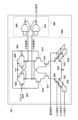
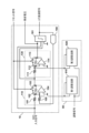
- FIG. 1 is a diagram showing a configuration of a two-stage continuous time ⁇ AD converter circuit according to a first embodiment.
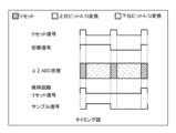
- 4 is an operation timing diagram of the two-stage continuous time ⁇ AD converter circuit according to the first embodiment.
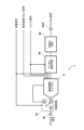
- FIG. 2 is a diagram showing a first configuration example of a continuous-time ⁇ converter in a two-stage continuous-time ⁇ converter circuit according to the first embodiment.
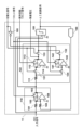
- FIG. 2 is a diagram showing a second configuration example of the continuous-time ⁇ converter in the two-stage continuous-time ⁇ converter circuit of the first embodiment.
- FIG. 4 is a diagram showing another example of the configuration of the integrator in the first embodiment. 4 is a diagram showing an example of the configuration of a comparison circuit in the two-stage continuous-time ⁇ converter circuit of the first embodiment;
- FIG. 1 is a diagram showing a configuration of a two-stage continuous time ⁇ AD converter circuit according to a first embodiment.
- 4 is an operation timing diagram of the two-stage continuous time ⁇ AD converter circuit according to the first
- FIG. 2 is a diagram showing an example of the configuration of a residual voltage holding circuit in the two-stage continuous time ⁇ converter circuit of the first embodiment.
- 4 is a diagram showing an example of the operation of a residual voltage holding circuit in the two-stage continuous time ⁇ converter circuit of the first embodiment.
- FIG. 13 is a diagram showing the configuration of a two-stage continuous time ⁇ AD converter circuit according to a second embodiment.
- FIG. 13 is a diagram showing a first configuration example of a continuous-time ⁇ converter in a two-stage continuous-time ⁇ converter circuit according to a second embodiment.
- FIG. 13 is a diagram showing a second configuration example of the continuous-time ⁇ converter in the two-stage continuous-time ⁇ converter circuit of the second embodiment.
- FIG. 13 is a diagram showing a third configuration example of the continuous-time ⁇ converter in the two-stage continuous-time ⁇ converter circuit of the second embodiment. 12 is a diagram showing the operation of the third configuration example shown in FIG. 11 .
- FIG. 13 is a diagram showing a configuration of a two-stage continuous time ⁇ AD converter circuit according to a third embodiment.
- FIG. 13 is a diagram showing a configuration of a two-stage continuous time ⁇ AD converter circuit according to a third embodiment.
- FIG. 13 is a diagram showing the configuration of a photoelectric conversion device according to a seventh embodiment.
- FIG. 1 is a diagram showing an example of the configuration of a photoelectric conversion system according to an embodiment.
- FIG. 1 is a diagram showing an example of the configuration of a photoelectric conversion system according to an embodiment.
- FIG. 13 is a diagram showing the configuration of a photoelectric conversion system or a moving body according to another embodiment.
- FIG. 13 is a diagram showing the configuration of a photoelectric conversion system or a moving body according to another embodiment.
- FIG. 13 is a diagram showing the configuration of an analog circuit unit in a two-stage continuous time ⁇ converter circuit according to a fourth embodiment.
- FIG. 13 is a diagram showing an example of the configuration of an analog circuit unit in a two-stage continuous time ⁇ converter circuit according to a fourth embodiment.
- FIG. 13 is a diagram showing a first configuration example of a switching circuit and a buffer circuit in a two-stage continuous time ⁇ converter circuit according to a fourth embodiment.
- FIG. 13 is a diagram showing the operation of a first configuration example of a switching circuit and a buffer circuit in a two-stage continuous time ⁇ converter circuit according to the fourth embodiment.
- FIG. 13 is a diagram showing a second configuration example of the switching circuit and the buffer circuit in the two-stage continuous time ⁇ converter circuit of the fourth embodiment.
- 13 is a diagram showing the operation of a second configuration example of the switching circuit and the buffer circuit in the two-stage continuous time ⁇ converter circuit of the fourth embodiment.
- 13 is a diagram showing the operation of a second configuration example of the switching circuit and the buffer circuit in the two-stage continuous time ⁇ converter circuit of the fourth embodiment.
- FIG. 13 is a diagram showing an example of the configuration of an analog circuit unit in a two-stage continuous time ⁇ converter circuit according to a fifth embodiment.
- FIG. 13 is a diagram showing an example of the configuration of a switching circuit and a buffer circuit in a two-stage continuous-time ⁇ converter circuit according to a fifth embodiment.
- 13 is a diagram showing the operation of a second configuration example of the switching circuit and the buffer circuit in the two-stage continuous time ⁇ converter circuit of the fifth embodiment.
- 13 is a diagram showing the operation of a switching circuit and a buffer circuit in a two-stage continuous-time ⁇ converter circuit according to a fifth embodiment.
- FIG. 13 is a diagram showing the configuration of a two-stage continuous time ⁇ AD converter circuit according to a sixth embodiment.
- FIG. 13 is a diagram showing a first configuration example of a continuous-time ⁇ converter in a two-stage continuous-time ⁇ converter circuit according to a sixth embodiment.
- FIG. 23 is a diagram showing a second configuration example of the continuous-time ⁇ converter in the two-stage continuous-time ⁇ converter circuit of the sixth embodiment.
- FIG. 2 is a diagram showing a configuration example of
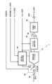
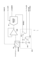
- the AD conversion circuit 1 shows the configuration of an AD conversion circuit 1 according to a first embodiment of the present disclosure.
- the AD conversion circuit 1 is configured as a two-stage continuous-time ⁇ AD conversion circuit.
- the AD conversion circuit 1 converts an analog signal provided to an input terminal IN into a digital signal and outputs it from an output terminal OUT.
- the AD conversion circuit 1 may include a continuous-time ⁇ AD converter 10 and a switching circuit 30.
- the AD conversion circuit 1 may also include a residual voltage holding circuit 20, a digital demodulation circuit 40, and a reconstruction circuit 50.
- the continuous-time ⁇ AD converter 10 may include an integration circuit that integrates a differential signal. During the first period, the switching circuit 30 provides the continuous-time ⁇ AD converter 10 with an analog signal provided to the input terminal IN.
- the switching circuit 30 provides the continuous-time ⁇ AD converter 10 with a voltage signal corresponding to the voltage output from the integration circuit of the continuous-time ⁇ AD converter 10 at the end of the first period.
- the first period is a period during which AD conversion is performed to generate a higher-order bit string of a digital signal corresponding to the analog signal provided to the input terminal IN.
- the second period is a period during which AD conversion is performed to generate a lower-order bit string of a digital signal corresponding to the analog signal provided to the input terminal IN.
- the higher-order bit string can be composed of multiple bits.
- the lower-order bit string can also be composed of multiple bits.
- the residual voltage holding circuit 20 holds (samples) a voltage signal corresponding to the residual voltage output from the continuous-time ⁇ AD converter 10 at the end of the first period, and supplies the voltage signal to the switching circuit 30 during the second period.
- the residual voltage holding circuit 20 can be controlled, for example, by a holding circuit reset signal and a sample signal.
- the continuous-time ⁇ AD converter 10 performs A/D conversion corresponding to the upper bit string, and the voltage signal corresponding to the residual voltage held by the residual voltage holding circuit 20 at the end of the first period is provided to the continuous-time ⁇ AD converter 10 by the switching circuit 30. Thereafter, in the second period, the continuous-time ⁇ AD converter 10 performs A/D conversion corresponding to the lower bit string.
- the time-series ⁇ modulated signal (upper bit string) output from the continuous-time ⁇ AD converter 10 in the first period is demodulated into a multi-bit digital signal by the digital demodulation circuit 40.
- the time-series ⁇ modulated signal (lower bit string) output from the continuous-time ⁇ AD converter 10 in the second period is demodulated into a multi-bit digital signal by the digital demodulation circuit 40.
- the reconstruction circuit 50 generates an output digital signal based on the digital signal of the upper bit string and the digital signal of the lower bit string demodulated by the digital demodulation circuit 40.
- the internal signal of the continuous-time ⁇ AD converter 10 and the internal signal of the digital demodulation circuit 40 are reset before the start of the first period and before the start of the second period in accordance with the reset signal.
- the AD conversion circuit 1 can be realized as a two-stage continuous-time ⁇ AD converter circuit by using one continuous-time ⁇ AD converter 10 and a residual voltage holding circuit 20.
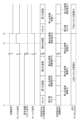
- FIG. 2 shows an operation timing diagram of the AD conversion circuit 1 shown in FIG. 1.
- the AD conversion circuit 1 a process in which the reconstruction circuit 50 outputs the final AD conversion result (final ADC result) (0) will be described.
- the continuous-time ⁇ AD converter 10 and the digital demodulation circuit 40 are reset.
- the holding circuit reset signal is in a high state
- the residual voltage holding circuit 20 is reset.
- the period from time t2 to t3 is the first period.
- the continuous-time ⁇ AD converter 10 starts A/D conversion corresponding to the upper bit string, and the residual voltage holding circuit 20 starts sampling the residual voltage (voltage signal corresponding to it). Also, at time t2, the digital demodulation circuit 40 starts demodulation processing of the upper bit string. At time t3, the A/D conversion corresponding to the upper bit string ends. At time t3, the residual voltage holding circuit 20 starts holding the residual voltage (a voltage signal corresponding to the residual voltage), which is the output voltage of the continuous-time ⁇ AD converter 10 at the end of the first period, and at the same time, the reconstruction circuit 50 acquires a multi-bit demodulated signal corresponding to the upper bit string.
- the reset signal goes high again, and the continuous-time ⁇ AD converter 10 and the digital demodulation circuit 40 are reset.
- the period from time t4 to t5 is the second period. From the point when the reset signal goes low at time t4, the continuous-time ⁇ AD converter 10 starts A/D conversion corresponding to the lower bit string, and the digital demodulation circuit 40 starts demodulation processing of the lower bit string. At time t5, the A/D conversion corresponding to the lower bit string ends. In response to this, the reconstruction circuit 50 acquires a multi-bit demodulated signal corresponding to the lower bit string.
- the reconstruction circuit 50 acquires a multi-bit demodulated signal corresponding to the lower bit string, and performs reconstruction processing using the multi-bit demodulated signal corresponding to the upper bit string described above, thereby outputting the final ADC result corresponding to the output digital signal.
- the AD conversion circuit 1 repeats the above A/D conversion to perform A/D conversion on any input analog signal. Note that it is assumed that the input analog signal is constant during the A/D conversion period corresponding to the upper bit string described above.
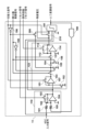
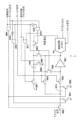
- FIG. 3 shows the configuration of a second-order continuous-time ⁇ AD converter as a first configuration example of the continuous-time ⁇ AD converter 10.
- the first configuration example of the continuous-time ⁇ AD converter 10 may include a first integrator 110, a second integrator 120, a comparator 180, and a digital-to-analog converter (DA converter) 190.
- the first integrator 110 may include, for example, resistors 101 and 105, a capacitor 102, a switch 103, and an amplifier 104.
- the second integrator 120 may include, for example, resistors 111 and 115, a capacitor 112, a switch 113, and an amplifier 114.
- the output of the switching circuit 30 is supplied to the input terminal of the first integrator 110 as an ADC input signal.
- the output of the first integrator 110 is supplied to the second integrator 120, and the output of the second integrator 120 is supplied to the comparator 180.
- the output of the comparator 180 is supplied to the DA converter 190, and the output of the DA converter 190 is supplied to the resistor 105 in the first integrator 110 and the resistor 115 in the second integrator 120.
- the output of the second integrator 120 is output as the residual voltage of the continuous-time ⁇ AD converter 10.
- the capacitors 102 and 112 are reset.
- the first integrator 110 integrates the difference signal between the ADC input signal and the output of the DA converter 190.
- the second integrator 120 integrates the difference signal between the output voltage of the first integrator 110 and the output of the DA converter 190.
- the comparator 180 receives the difference signal between the output voltage of the second integrator 120 and the reference signal, and performs a comparison operation using a clock signal (not shown).
- the DA converter 190 outputs an analog voltage according to the output signal of the comparator 180.
- the DA converter 190 can be configured to output an analog voltage according to an input signal according to, for example, a 1-bit transfer function shown in equation (1).
- DACin is the output signal of comparator 180
- Vr is a reference signal (not shown) in the continuous-time ⁇ type AD converter 10
- DACout is the output signal of DA converter 190, with the reference signal being 0.
- the AD conversion circuit 1 in FIG. 3 repeatedly performs integration operations, comparison operations, and digital-to-analog conversion during the period from when the reset signal changes from a low state to a high state.
- the AD conversion circuit 1 is configured as a second-order continuous-time ⁇ type AD conversion circuit. Also, in the example of FIG. 3, the AD conversion circuit 1 has a 1-bit configuration for both the comparator 180 and the DA converter 190. However, the comparator 180 and the DA converter 190 may be multi-bit, and the resistor 105 of the first integrator 110 and the resistor 115 of the second integrator 120 may be increased according to the resolution of the comparator 180 and the DA converter 190 and connected in parallel. By configuring the comparator 180 and the DA converter 190 with multiple bits, the AD conversion speed of the continuous-time ⁇ type AD converter 10 can be increased.
- a third-order or higher continuous-time ⁇ type AD converter may be configured by adding one or more integrators between the second integrator 120 and the comparator 180. By increasing the number of integrators, the AD conversion speed of the continuous-time ⁇ type AD converter 10 can be increased.
- FIG. 4 shows the configuration of a second-order continuous-time ⁇ AD converter having a feedforward path as a second configuration example of the continuous-time ⁇ AD converter 10.
- the second configuration example of the continuous-time ⁇ AD converter 10 may include a first integrator 110, a second integrator 130, a four-input comparator 181, and a digital-to-analog converter (DA converter) 190.
- the first integrator 110 may include, for example, resistors 101 and 105, a capacitor 102, a switch 103, and an amplifier 104.
- the second integrator 130 may include a resistor 111, a capacitor 112, a switch 113, and an amplifier 114.
- the output of the switching circuit 30 is supplied to the input terminal of the first integrator 110 as an ADC input signal.
- the output of the first integrator 110 is supplied to the second integrator 130, and the output of the second integrator 130 is supplied to a four-input comparator 181.
- the output of the four-input comparator 181 is supplied to a DA converter 190, and the output of the DA converter 190 is supplied to the resistor 105 in the first integrator 110.
- the operation of the second configuration example shown in FIG. 4 is similar to the operation of the first configuration example shown in FIG. 3.
- a signal supplied as an ADC input signal from the switching circuit 30 is supplied to the four-input comparator 181.
- the output of the first integrator 110 and the output of the second integrator 130 are supplied to the four-input comparator 181.
- the AD conversion circuit 1 is configured as a second-order continuous-time ⁇ ADC.
- the AD conversion circuit 1 has a 1-bit configuration for both the 4-input comparator 181 and the DA converter 190.
- the 4-input comparator 181 and the DA converter 190 may be multi-bit, and the resistor 105 of the first integrator 110 may be increased according to the resolution of the 4-input comparator 181 and the DA converter 190 and connected in parallel.
- a third-order or higher continuous-time ⁇ AD converter may be configured by adding one or more integrators between the second integrator 130 and the 4-input comparator 181.
- the integrator 140 can include switches 1401 and 1402, a capacitor 1403, a transconductance 1404, and an inverter 1405.
- the switch 1401 is controlled by a reset signal
- the switch 1402 is controlled by a reset signal inverted by the inverter 1405.
- the capacitor 1403 is reset.
- an integration operation is performed by the capacitor 1403 and the difference current between the current generated by the transconductance 1404 in response to the input signal and the output signal current of the DA converter 190.
- the output of the DA converter 190 is connected to the output of the transconductance 1404.
- This configuration achieves the same functionality as an integrator consisting of resistors, capacitors, and amplifiers while reducing power consumption.
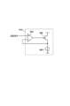
- the four-input comparator 181 may include a latch-type comparator 650 and an SR flip-flop 660.
- the latch-type comparator 650 may include, for example, PMOS transistors 601, 602, 603, and 604, NMOS transistors 610, 611, 612, and 613, and input transistors 620, 621, 622, 630, 631, and 632.
- the SR flip-flop 660 may be composed of NAND gates 640 and 641. In the example configuration shown in FIG.
- the latch-type comparator 650 of the four-input comparator 181 when the clock signal is in a low state, the latch-type comparator 650 of the four-input comparator 181 is in a reset state, the output signals, comparison result 1 and comparison result 2, are in a high state, and the SR flip-flop 660 is in a holding state.
- the latch-type comparator 650 When the clock signal is in a high state, the latch-type comparator 650 generates an internal signal corresponding to the difference voltage between each of the three input signals and the reference signal, and outputs the results according to these internal signals as comparison results 1 and 2.
- the SR flip-flop 660 outputs signals corresponding to comparison results 1 and 2.
- comparison result 1 will be in a low state
- comparison result 2 will be in a high state
- the output signal will be in a high state.
- the residual voltage holding circuit 20 includes, for example, switches 701, 702, 703, 710, 711, 720, an amplifier 730, and a sample capacitor 740.
- the switches 701 and 702 are controlled by a switching signal.
- the switch 703 is controlled by a sample signal.
- the switches 710 and 711 are controlled by an inverted switching signal.
- the switch 720 is controlled by a holding circuit reset signal. When the switching signal is in a high state, the holding circuit reset signal is in a high state, and the sample signal is in a low state, the sample capacitor 740 is reset.
- the holding circuit set signal When the switching signal is in a high state, the holding circuit set signal is in a low state, and the sample signal is in a high state, a voltage signal corresponding to the input signal (the output of the continuous-time ⁇ type AD converter 10) is sampled by the sample capacitor 740.
- the voltage signal sampled at this time is the residual voltage after AD conversion corresponding to the upper bit string.
- the holding circuit reset signal When the switching signal is low, the holding circuit reset signal is low, and the sample signal is low, the sampled voltage signal is held in the sample capacitor 740.
- the input signal sampling operation and the holding of the sampled input signal are realized by one amplifier 730, which makes it possible to reduce power consumption and the mounting area.
- the operation period of the residual voltage holding circuit 20 can be reduced by setting the switching signal to a high state at any time until the end of the AD conversion of the upper bit string, and power consumption can be reduced.
- the digital demodulation circuit 40 shown in FIG. 1 performs digital signal processing according to equation (2) on a 1-bit time series ⁇ modulated signal that corresponds to the upper bit string of the continuous-time ⁇ AD converter 10, thereby outputting a multi-bit demodulated signal.
- M indicates the oversampling ratio in the AD conversion corresponding to the upper bit string in the continuous-time ⁇ AD converter 10
- i indicates the time index of the comparison result output in time series.
- the digital demodulation circuit 40 outputs a multi-bit demodulated signal by performing digital signal processing according to equation (3) on the 1-bit time series ⁇ modulated signal corresponding to the lower bit string in the continuous-time ⁇ AD converter 10.
- N indicates the oversampling ratio in the AD conversion corresponding to the lower bit string in the continuous-time ⁇ AD converter 10
- i indicates the time index of the comparison result that is output in time series.
- the reconstruction circuit 50 shown in FIG. 1 performs reconstruction processing on the upper bit demodulated signal and the lower bit demodulated signal according to equation (4).
- this reconstruction processing if the signal obtained by combining the upper bit demodulated signal and the lower bit demodulated signal is assumed to be a decimal number (actually it is a binary signal), it is normalized so that the maximum value in decimal is 1. For example, if a signal is generated that has a value of 15 when assumed to be a decimal number, this reconstruction processing multiplies the upper bit demodulated signal and the lower bit demodulated signal by 1/15. In this way, a final digital signal is obtained that is the final A/D conversion result for M+L bits, normalized so that the maximum value when assumed to be converted to a decimal number is 1.
- M and N may be the same or different.
- the AD conversion circuit 1 is configured as a two-stage continuous-time ⁇ AD conversion circuit.
- the AD conversion circuit 1 converts an analog signal provided to an input terminal IN into a digital signal and outputs it from an output terminal OUT.
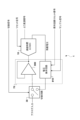
- the AD conversion circuit 1 may include a continuous-time ⁇ AD converter 11 and a switching circuit 30.
- the AD conversion circuit 1 may also include a digital demodulation circuit 40 and a reconstruction circuit 50.
- the continuous-time ⁇ AD converter 11 may include an integration circuit that integrates a difference signal. During the first period, the switching circuit 30 provides the continuous-time ⁇ AD converter 10 with an analog signal provided to the input terminal IN.
- the switching circuit 30 provides the continuous-time ⁇ AD converter 11 with a voltage signal corresponding to the voltage output from the integration circuit of the continuous-time ⁇ AD converter 11 at the end of the first period.
- the first period is a period during which AD conversion is performed to generate a higher-order bit string of a digital signal corresponding to the analog signal provided to the input terminal IN.
- the second period is a period during which AD conversion is performed to generate a lower-order bit string of a digital signal corresponding to the analog signal provided to the input terminal IN.
- the higher-order bit string can be composed of multiple bits.
- the lower-order bit string can also be composed of multiple bits.
- the continuous-time ⁇ AD converter 11 holds (samples) a voltage signal corresponding to the residual voltage output from the continuous-time ⁇ AD converter 11 at the end of the first period, and supplies the voltage signal to the switching circuit 30 during the second period.
- the continuous-time ⁇ AD converter 11 performs A/D conversion corresponding to the upper bit string. Also, a voltage signal corresponding to the residual voltage held (sampled) by the continuous-time ⁇ AD converter 11 at the end of the first period is provided to the input terminal of the continuous-time ⁇ AD converter 11 via the switching circuit 30. Thereafter, in the second period, the continuous-time ⁇ AD converter 11 performs A/D conversion corresponding to the lower bit string.
- the time-series ⁇ modulated signal (upper bit string) output from the continuous-time ⁇ AD converter 11 in the first period is demodulated by the digital demodulation circuit 40 into a multi-bit digital signal.
- the time-series ⁇ modulated signal (lower bit string) output from the continuous-time ⁇ AD converter 10 in the second period is demodulated by the digital demodulation circuit 40 into a multi-bit digital signal.
- the reconstruction circuit 50 generates an output digital signal based on the digital signal of the upper bit string and the digital signal of the lower bit string demodulated by the digital demodulation circuit 40.
- the internal signal of the continuous time ⁇ AD converter 11 and the internal signal of the digital demodulation circuit 40 are reset before the start of the first period and before the start of the second period in accordance with the reset signal. With this configuration, the voltage signal corresponding to the residual voltage at the end of the first period is held in the continuous time ⁇ AD converter 11, thereby realizing the AD conversion circuit 1 as a two-stage continuous time ⁇ AD conversion circuit.
- FIG. 9 shows the configuration of a second-order continuous-time ⁇ AD converter as a first configuration example of the continuous-time ⁇ AD converter 11.
- the continuous-time ⁇ AD converter 11 of the first configuration example may include a first integrator 110, a second integrator 121, a comparator 180, a digital-to-analog converter (DA converter) 190, and an inverter 195.
- the first integrator 110 may include, for example, resistors 101 and 105, a capacitor 102, a switch 103, and an amplifier 104.
- the second integrator 121 may include, for example, resistors 111 and 115, capacitors 112 and 141, switches 113, 131, 132, 133, 134, and 142, and amplifiers 114 and 143.
- the output of the switching circuit 30 is supplied to the input terminal of the first integrator 110 as an ADC input signal.
- the output of the first integrator 110 is supplied to the second integrator 121, and the output of the second integrator 121 is supplied to the comparator 180.
- the output of the comparator 180 is supplied to the DA converter 190, and the output of the DA converter 190 is supplied to the resistor 105 in the first integrator 110 and the resistor 115 in the second integrator 121.
- the output of the second integrator 121 is output as the residual voltage of the continuous-time ⁇ AD converter 11.
- an integrator consisting of resistors 111 and 115, switches 113, 131 and 133, capacitor 112 and amplifier 114 performs an integration operation in the A/D conversion corresponding to the upper bit string described above. After the A/D conversion corresponding to the upper bit string is completed, the switching signal goes low and a voltage signal corresponding to the residual voltage is held by capacitor 112 and amplifier 114.
- an integrator consisting of resistors 111 and 115, switches 132, 134 and 142, capacitor 141 and amplifier 143 performs an integration operation in the A/D conversion corresponding to the lower bit string.
- the second integrator 121 realizes a residual voltage holding circuit, thereby reducing the control signal and the number of switches, thereby reducing the mounting area.
- the AD conversion circuit 1 is configured as a second-order continuous time ⁇ type AD circuit.
- the AD conversion circuit 1 has a 1-bit configuration for both the comparator 180 and the DA converter 190.
- the comparator 180 and the DA converter 190 may be multi-bit, and the resistor 105 of the first integrator 110 and the resistor 115 of the second integrator 121 may be increased according to the resolution of the comparator 180 and the DA converter 190 and connected in parallel.
- a third-order or higher continuous time ⁇ type AD converter may be configured by adding one or more integrators between the second integrator 121 and the comparator 180. By increasing the number of integrators, the AD conversion speed of the continuous time ⁇ type AD converter 10 can be increased.
- the second configuration example of the continuous-time ⁇ AD converter 11 may include a first integrator 110, a second integrator 122, a four-input comparator 181, a digital-to-analog converter (DA converter) 190, and an inverter 195.
- the first integrator 110 may include, for example, resistors 101, 105, a capacitor 102, a switch 103, and an amplifier 104.
- the second integrator 122 may include, for example, resistor 111, capacitors 112, 141, switches 113, 131, 132, 133, 134, 142, and amplifiers 114, 143.
- the operation of the continuous-time ⁇ AD converter 11 of the second configuration example shown in FIG. 10 is similar to the operation of the continuous-time ⁇ AD converter 11 of the first configuration example shown in FIG. 9, and has the advantages described in the second configuration example of the first embodiment (FIG. 4).
- the AD conversion circuit 1 is configured as a second-order continuous time ⁇ type AD circuit. Also, in the example of FIG. 10, the AD conversion circuit 1 has a 1-bit configuration for both the 4-input comparator 181 and the DA converter 190. However, the 4-input comparator 181 and the DA converter 190 may be multi-bit, and the resistor 105 of the first integrator 110 may be increased according to the resolution of the 4-input comparator 181 and the DA converter 190 and connected in parallel. Also, a third-order or higher continuous time ⁇ type AD converter may be configured by adding one or more integrators between the second integrator 131 and the 4-input comparator 181.
- FIG. 11 shows a configuration of a second-order continuous-time ⁇ AD converter having a feedforward path as a third configuration example of the continuous-time ⁇ AD converter 11.
- the third configuration example of the continuous-time ⁇ AD converter 11 may include a first integrator 110, a second integrator 123, a four-input comparator 181, a DA converter 190, an inverter 195, switches 200 and 210, and inverters 195 and 196.
- the first integrator 110 may include, for example, resistors 101 and 105, a capacitor 102, a switch 103, and an amplifier 104.
- the second integrator 123 may include, for example, capacitors 112 and 154, switches 113, 131, 151, 152, 153, 155, and 156, and amplifiers 114 and 157.
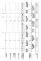
- Figure 12 shows the operation of the continuous-time ⁇ AD converter 11 of the third configuration example of Figure 11.
- the operation of the second integrator 123 differs between A/D conversion corresponding to the upper bit string and A/D conversion corresponding to the lower bit string.
- an integration operation is performed by a switched capacitor integrator composed of capacitor 112, switches 113, 131, 153, 155, 156, and amplifier 114.
- a gm-C integrator composed of switches 153, 156, 151, 152, and amplifier 157.
- a voltage signal corresponding to the residual voltage signal is output by a holding circuit composed of capacitor 112 and amplifier 114.
- the internal signal of the second integrator 123 supplied to the four-input comparator 181 differs between A/D conversion corresponding to the upper bit string and A/D conversion corresponding to the lower bit string, and is switched by switches 200 and 210.
- the AD conversion circuit 1 is configured as a second-order continuous time ⁇ AD circuit. Also, in the example of FIG. 11, the AD conversion circuit 1 has a 1-bit configuration for both the 4-input comparator 181 and the DA converter 190. However, the 4-input comparator 181 and the DA converter 190 may be multi-bit, and the resistor 105 of the first integrator 110 may be increased according to the resolution of the 4-input comparator 181 and the DA converter 190 and connected in parallel. Also, a third-order or higher continuous time ⁇ AD converter may be configured by adding one or more integrators between the first integrator 110 and the second integrator 123.
- FIG 13 shows the configuration of the AD conversion circuit 1 of the third embodiment of the present disclosure.
- the AD conversion circuit 1 is configured as a two-stage continuous-time ⁇ AD conversion circuit.
- the AD conversion circuit 1 converts an analog signal provided to the input terminal IN into a digital signal and outputs it from the output terminal OUT.
- the AD conversion circuit 1 may include a continuous-time ⁇ AD converter 10 and a switching circuit 30.
- the AD conversion circuit 1 may also include a residual voltage holding circuit 20, a digital demodulation circuit 40, a reconstruction circuit 50, and a digital gain adjustment circuit 60.
- the continuous-time ⁇ AD converter 10 may include an integration circuit that integrates a differential signal. During the first period, the switching circuit 30 provides the analog signal provided to the input terminal IN to the continuous-time ⁇ AD converter 10.
- the switching circuit 30 provides the continuous-time ⁇ AD converter 10 with a voltage signal corresponding to the voltage output from the integrator circuit of the continuous-time ⁇ AD converter 10 at the end of the first period.
- the first period is a period during which AD conversion is performed to generate a higher-order bit string of a digital signal corresponding to the analog signal provided to the input terminal IN.
- the second period is a period during which AD conversion is performed to generate a lower-order bit string of a digital signal corresponding to the analog signal provided to the input terminal IN.
- the higher-order bit string may be composed of multiple bits.
- the lower-order bit string may be composed of multiple bits.
- the residual voltage holding circuit 20 holds (samples) a voltage signal corresponding to the residual voltage output from the continuous-time ⁇ AD converter 10 at the end of the first period, and supplies the voltage signal to the switching circuit 30 during the second period.
- the residual voltage holding circuit 20 can be controlled, for example, by a holding circuit reset signal and a sample signal.
- the continuous-time ⁇ AD converter 10 performs A/D conversion corresponding to the upper bit string, and the voltage signal corresponding to the residual voltage held by the residual voltage holding circuit 20 at the end of the first period is provided to the continuous-time ⁇ AD converter 10 by the switching circuit 30. Thereafter, in the second period, the continuous-time ⁇ AD converter 10 performs A/D conversion corresponding to the lower bit string.
- the time-series ⁇ modulated signal (upper bit string) output from the continuous-time ⁇ AD converter 10 in the first period is demodulated into a digital signal of multiple bits by the digital demodulation circuit 40.
- the time-series ⁇ modulated signal (lower bit string) output from the continuous-time ⁇ AD converter 10 in the second period is demodulated into a digital signal of multiple bits by the digital demodulation circuit 40.
- the reconstruction circuit 50 generates an output digital signal based on the digital signal of the upper bit string and the digital signal of the lower bit string demodulated by the digital demodulation circuit 40.
- the internal signal of the continuous-time ⁇ AD converter 10, the voltage signal held by the residual voltage holding circuit 20, and the internal signal of the digital demodulation circuit 40 are reset before the start of the first period and before the start of the second period in accordance with the reset signal.
- the digital gain adjustment circuit 60 may be disposed between the digital demodulation circuit 40 and the reconstruction circuit 50.
- the digital gain adjustment circuit 60 may perform gain adjustment on the digital signal output from the digital demodulation circuit 40 and supply the gain-adjusted digital signal to the reconstruction circuit 50.
- the digital gain adjustment circuit 60 may be configured to perform gain adjustment on the digital signal of the lower bit string output from the digital demodulation circuit 40 and not perform gain adjustment on the digital signal of the higher bit string output from the digital demodulation circuit 40.
- the digital gain (correction value) applied by the digital gain adjustment circuit 500 may be acquired prior to AD conversion of the analog signal to be AD converted.
- a correction value may be generated by inputting an analog signal of a reference value to the AD conversion circuit 2 and comparing the digital signal (expected value) that is originally obtained with the digital signal actually output from the AD conversion circuit 2. To further improve the accuracy of the correction, it is preferable to perform the correction value acquisition operation using analog signals of multiple reference values with different values.
- circuit-specific errors may occur, such as a gain error caused by the finite gain of the amplifier circuit.
- gain errors may cause errors between the most significant bit demodulated signal and the least significant bit demodulated signal from the theoretical values shown in equations (2) and (3). This may result in nonlinear distortion of the A/D converter, degrading performance.
- the gain error of the residual voltage holding circuit is digitally corrected, improving nonlinear distortion.
- FIG. 14 shows another example configuration of the third embodiment of the present disclosure.
- the example configuration shown in FIG. 14 has a configuration in which a digital gain adjustment circuit 60 is added to the second embodiment (FIG. 8).
- the configuration and operation of the analog circuit section in the two-stage continuous-time ⁇ AD converter circuit 1 of the fourth embodiment will be described with reference to Figures 18, 19, 20A, 20B, 21A, 21B, 21C, and 22. Note that matters not mentioned as the fourth embodiment may follow the first to third embodiments.
- the AD converter circuit 1 may include a continuous-time ⁇ AD converter 10, a switching circuit 30, and a buffer circuit 70. Although not shown, the continuous-time ⁇ AD converter circuit 1 may include a digital demodulation circuit 40 and a reconstruction circuit 50, similar to the first to fourth embodiments.
- the switching circuit 30 provides the analog signal provided to the input terminal IN to the buffer circuit 70, and during the second period following the first period, the switching circuit 30 provides the residual voltage output from the continuous-time ⁇ AD converter 10 at the end of the first period to the buffer circuit 70.
- the first period is a period during which AD conversion is performed to generate a higher-order bit string of a digital signal corresponding to the analog signal provided to the input terminal IN.
- the second period is a period during which AD conversion is performed to generate a lower-order bit string of a digital signal corresponding to the analog signal provided to the input terminal IN.
- the higher-order bit string can be composed of multiple bits.
- the lower-order bit string can be composed of multiple bits.
- the buffer circuit 70 has a function of holding the residual voltage supplied from the continuous-time ⁇ AD converter 10 via the switching circuit 30 at the end of the first period for the second period.
- the buffer circuit 70 is controlled by a holding circuit reset signal and a sample signal.
- the buffer circuit 70 buffers the analog signal supplied to the input terminal IN of the switching circuit 30 and output from the switching circuit 30, and outputs it to the continuous-time ⁇ ADC 10.
- the buffer circuit 70 holds the residual voltage output from the continuous-time ⁇ ADC 10 at the end of the first period in which the upper bit string is generated.
- the buffer circuit 70 outputs a voltage obtained by buffering the held residual voltage, i.e., a voltage corresponding to the residual voltage, to the continuous-time ⁇ ADC 10.
- the buffer circuit 70 has a function of holding a voltage signal corresponding to the residual voltage output from the integrating circuit of the continuous-time ⁇ ADC 10 at the end of the first period.
- the continuous-time ⁇ ADC 1 may have a first integrator 110 in the input stage, as illustrated in FIG. 3.
- the first integrator 110 has a voltage-current conversion circuit
- a DC voltage corresponding to the input analog signal voltage flows in the voltage-current conversion circuit.
- a source follower circuit is used as a circuit that supplies an analog signal to the continuous-time ⁇ AD circuit 10
- a DC current value corresponding to the voltage value of the analog signal flows in addition to the bias current. This may cause a gain deviation in the source follower circuit, degrading the linearity of the analog signal.
- the fifth embodiment by arranging a buffer circuit 70 in the input path of the analog signal, the DC current flowing in the source follower circuit according to the voltage value of the analog signal is suppressed, improving linearity.
- linearity can be improved without increasing the circuit components and power consumption.
- FIG. 19 shows a first configuration example of a buffer circuit 70 having a function of holding a residual voltage.
- the buffer circuit 70 has an amplifier 800 and a voltage holding circuit 810.
- the voltage holding circuit 810 is controlled by a holding circuit reset signal and a sample signal, and holds and outputs the residual voltage supplied from the continuous-time ⁇ ADC 10.
- the buffer circuit 70 can be realized, for example, by configuring a voltage follower circuit using the two-input, one-output amplifier 800.
- the analog signal provided to the input terminal IN is buffered using the amplifier 800.
- the voltage held by the voltage holding circuit 810 (which has the function of holding the residual voltage) at the end of the first period is held and buffered using the amplifier 800 to generate a voltage signal.
- the voltage holding circuit 810 is composed of switches 811, 812, and a capacitor 813.
- the analog signal supplied to the input terminal IN is supplied to the buffer circuit 70 composed of an amplifier 800 (voltage follower circuit), and the analog signal buffered by the voltage follower circuit is supplied to the continuous-time ⁇ ADC 10.
- the voltage follower circuit continues to buffer the analog signal until the integrator accumulation of the A/D conversion of the last bit of the high-order bit string is completed.
- the switching circuit 30 supplies the output signal of the voltage holding circuit 810 to the continuous-time ⁇ ADC 10. Note that the holding circuit reset signal goes high at the start of the first period in which AD conversion is performed to generate the upper bit string, and can go low at any time before the final integrator accumulation operation in the first period.
- FIG. 21A and 21B show a second configuration example and a timing chart of a circuit including the switching circuit 30 and the buffer circuit 70, respectively.
- FIG. 21C shows a schematic diagram of the transition of the state of the buffer circuit.
- the switching circuit 30 and the buffer circuit 70 are composed of switches 851, 852, 853, 854, 855, 856, 857, and 858, a capacitance 813, an OR circuit 870, and an amplifier 800.
- the switching signal is high, the sample signal is low, the holding circuit reset signal is high, and the hold signal is low, resulting in state S211 in FIG. 21C.
- the analog signal is buffered by the voltage follower circuit composed of the amplifier 800 and the switch 858, and the accumulated charge of the capacitance 813 is reset using the switches 852 and 855.
- the holding circuit reset signal becomes low, and the reset operation is completed.
- the sample signal goes high, and switches 857, 852 and capacitor 813 transition to state S212 in FIG. 21C.
- the residual signal is sampled.
- the switching signal goes low, the sample signal goes low, and the hold signal goes high, and amplifier 800, capacitor 813, and switches 854, 856, and 853 transition to state S213 in FIG. 21C.
- the circuit forms a feedback circuit, and buffers the signal sampled at time t2 while holding it.
- the AD converter circuit 1 may include a continuous-time ⁇ AD converter 10, a switching circuit 30, and a buffer circuit 80. Although not shown, the continuous-time ⁇ AD converter circuit 1 may include a digital demodulation circuit 40 and a reconstruction circuit 50, similar to the first to fourth embodiments.
- the switching circuit 30 provides the analog signal provided to the input terminal IN to the buffer circuit 70, and during the second period following the first period, the switching circuit 30 provides the residual voltage output from the continuous-time ⁇ AD converter 10 at the end of the first period to the buffer circuit 70.
- the first period is a period during which AD conversion is performed to generate a higher-order bit string of a digital signal corresponding to the analog signal provided to the input terminal IN.
- the second period is a period during which AD conversion is performed to generate a lower-order bit string of a digital signal corresponding to the analog signal provided to the input terminal IN.
- the higher-order bit string can be composed of multiple bits.
- the lower-order bit string can be composed of multiple bits.
- the buffer circuit 80 has a function of holding an analog signal and a residual voltage.
- the buffer circuit 80 is controlled by a holding circuit reset signal and a sample signal.
- the buffer circuit 80 holds (samples and holds) an analog signal that is supplied to the input terminal IN of the switching circuit 30 and output from the switching circuit 30 at the start of the first period in which A/D conversion for generating the upper bit string is performed, and buffers the held analog signal and outputs it over the first period.
- the buffer circuit 80 has a function of holding an analog signal provided to the input terminal IN at the start of the first period.
- the buffer circuit 70 holds (samples and holds) a residual voltage output from the continuous-time ⁇ ADC 10 at the end of the first period in which the upper bit string is generated.
- the buffer circuit 70 outputs a voltage obtained by buffering the held residual voltage, i.e., a voltage corresponding to the residual voltage, to the continuous-time ⁇ ADC 10.
- the buffer circuit 80 has the function of holding a voltage signal corresponding to the residual voltage output from the integration circuit of the continuous-time ⁇ ADC 10 at the end of the first period.
- the holding circuit that holds the residual voltage is added with the functionality of a buffer circuit, and also with the functionality of sampling and holding an analog signal. This allows the sampling of the analog signal and the holding period for providing the analog signal to the continuous time ⁇ AD conversion circuit to be pipelined operations.
- the pipeline operation of the circuit makes it possible to speed up the A/D conversion.
- 23A and 23B show a specific example of the configuration of a circuit including the switching circuit 30 and the buffer circuit 80, and a timing chart.
- the circuit is composed of switches 860, 861, 862, 863, 864, 865, 866, 867, 868, 869, capacitors 815 and 816, AND circuits 875, 878, 880, OR circuit 877, inverter circuits 876 and 879, and amplifier 801.
- the switching signal is high, the sample signal is high, the holding circuit reset signal is low, and the hold signal is low, resulting in state S231 in FIG. 23C.
- the feedback circuit composed of amplifier 801, capacitor 816, and switches 865 and 866 buffers the sampled residual voltage, while the analog signal is sampled by capacitor 815 using switches 860 and 862.
- the switching signal is low, the sample signal is low, the holding circuit reset signal is high, and the hold signal is high, resulting in state S232 in FIG. 23C.
- the feedback circuit composed of the amplifier 801, the capacitance 815, and the switches 863 and 864 buffers the sampled analog signal, while resetting the capacitance 816 using the switches 867 and 868.
- the holding circuit reset signal becomes low, completing the reset operation of the capacitance 816.
- the sample signal becomes high, the hold signal becomes low, and the residual voltage is sampled by the circuit composed of the capacitance 816 and the switches 867 and 869.
- the switching signal becomes high, the sample signal becomes low, and the hold signal becomes high, resulting in state S234 in FIG. 23C.
- a feedback circuit consisting of an amplifier 801, a capacitor 816, and switches 865 and 866 buffers the sampled residual voltage, while the capacitor 815 is reset using switches 861 and 862.
- the analog signal provided to the input terminal IN is held and buffered using the amplifier 801.
- the voltage held by the holding circuit at the end of the first period is held and buffered using the amplifier 801 to generate a voltage signal.
- FIG. 24 shows the configuration of the AD converter circuit 1 of the sixth embodiment.
- the AD converter circuit 1 may include a continuous-time ⁇ ADC 10, a residual voltage holding circuit 20, a switching circuit 30, a digital demodulation circuit 40, a reconstruction circuit 50, a voltage adjustment circuit 90, and a buffer circuit 95.
- the continuous-time ⁇ AD converter 10 may include an integration circuit that integrates a differential signal. During the first period, the switching circuit 30 provides the analog signal provided to the input terminal IN to the continuous-time ⁇ AD converter 10 via the buffer circuit 95.
- the switching circuit 30 provides the continuous-time ⁇ AD converter 10 with a voltage signal via the buffer circuit 95 that corresponds to the voltage output from the integrator circuit of the continuous-time ⁇ AD converter 10 at the end of the first period.
- the internal voltage of the continuous-time ⁇ ADC 10 during the AD conversion period is adjusted by the voltage adjustment circuit 90 based on the adjustment signal to within a range close to the signal value of the adjustment signal.
- the continuous-time ⁇ ADC 10 may include a first integrator 110, a second integrator 120, a comparator 180, and a DA converter 190.
- the first integrator 110 may include, for example, resistors 101 and 105, a capacitor 102, a switch 103, and an amplifier 104.
- the second integrator 120 may include, for example, resistors 111 and 115, a capacitor 112, a switch 113, and an amplifier 114.
- the voltage adjustment circuit 90 may include a first adjustment circuit 910 and a second voltage adjustment circuit 920.
- the operation of the continuous-time ⁇ ADC 10 shown in FIG. 25 is similar to the operation of the continuous-time ⁇ ADC 10 shown in FIG. 3.
- the output of the first integrator 110 is supplied to the second integrator 120, and the output of the second integrator 120 is supplied to the comparator 180.
- the output of the comparator 180 is also supplied to the DA converter 190, and the output of the DA converter 190 is supplied to the resistor 105 in the first integrator 110 and the resistor 115 in the second integrator 120.
- the output of the second integrator 120 is output as the residual voltage of the continuous-time ⁇ ADC 10.
- a first internal signal at a first internal node N1 to which resistors 101, 105, capacitor 102, switch 103, and amplifier 104 are connected is connected to an adjustment node of a first adjustment circuit 910.
- the first internal signal at the first internal node N1 is adjusted by the first adjustment circuit 910 to within a proximity range (in other words, a predetermined range) of the signal value of the adjustment signal input to the first adjustment circuit 910.
- a second internal signal at a second internal node N2 to which resistors 111, 115, capacitor 112, switch 113, and amplifier 114 are connected is adjusted by the second adjustment circuit 920 to within a proximity range (in other words, a predetermined range) of the adjustment signal input to the second adjustment circuit 920.
- a proximity range in other words, a predetermined range
- FIG. 25 shows an example of a single-phase circuit configuration
- the voltages of the internal nodes can be adjusted with a similar configuration even when the first integrator 110 and the second integrator 120 are differential circuits.
- the voltage input as the adjustment signal is a common-mode signal
- the voltages of the first and second internal nodes adjusted by the first and second adjustment circuits are common-mode voltages.
- the AD conversion circuit 1 is configured as a second-order continuous-time ⁇ ADC. Also, in the example of FIG. 25, the AD conversion circuit 1 has a 1-bit configuration for both the comparator 180 and the DA converter 190. However, the comparator 180 and the DA converter 190 may be multi-bit, and the resistor 105 of the first integrator 110 and the resistor 115 of the second integrator 120 may be increased according to the resolution of the comparator 180 and the DA converter 190 and connected in parallel. By configuring the comparator 180 and the DA converter 190 with multiple bits, the AD conversion speed of the continuous-time ⁇ AD converter 10 can be increased.
- a third-order or higher continuous-time ⁇ AD converter may be configured by adding one or more integrators between the second integrator 120 and the comparator 180. By increasing the number of integrators, the AD conversion speed of the continuous-time ⁇ AD converter 10 can be increased.
- FIG. 26 shows a second configuration example of the continuous-time ⁇ AD converter 11 of the sixth embodiment.
- the continuous-time ⁇ ADC 10 may include a first integrator 110, a second integrator 130, a four-input comparator 181, and a DA converter 190.
- the first integrator 110 may include, for example, resistors 101 and 105, a capacitor 102, a switch 103, and an amplifier 104.
- the second integrator 130 may include, for example, a resistor 111, a capacitor 112, a switch 113, and an amplifier 114.
- the voltage adjustment circuit 90 may include a first adjustment circuit 910 and a second voltage adjustment circuit 920.
- the output of the first integrator 110 is supplied to the second integrator 120, and the output of the second integrator 120 is supplied to the four-input comparator 181.
- the output of the four-input comparator 181 is supplied to the DA converter 190, and the output of the DA converter 190 is supplied to the resistor 105 in the first integrator 110.
- the output of the second integrator 130 is output as the residual voltage of the continuous-time ⁇ ADC 10.
- the first internal signal at the first internal node to which the resistors 101, 105, the capacitor 102, the switch 103, and the amplifier 104 are connected is connected to the adjustment node of the first adjustment circuit 910.
- the first internal signal at the internal node is adjusted by the first adjustment circuit 910 to within the vicinity range of the signal value of the adjustment signal input to the first adjustment circuit 910.
- the second internal signal at the second internal node to which the resistor 111, the capacitor 112, the switch 113, and the amplifier 114 are connected is adjusted by the second adjustment circuit 920 to within the vicinity range of the adjustment signal input to the second adjustment circuit 920.
- FIG. 26 shows an example of a single-phase circuit configuration
- the internal voltage can be adjusted with a similar configuration even when the first integrator 110 and the second integrator 120 are differential circuits.
- the voltage input as the adjustment signal is a common-mode signal
- the first and second internal voltages adjusted by the first and second adjustment circuits are common-mode voltages.
- the operation of the continuous time ⁇ ADC 10 shown in FIG. 26 is similar to that of the continuous time ⁇ ADC 10 shown in FIG. 3.
- a signal supplied as an ADC input signal from the switching circuit 30 is supplied to a four-input comparator 181.
- the output of the first integrator 110 and the output of the second integrator 130 are also supplied to the four-input comparator 181.
- the AD conversion circuit 1 is configured as a second-order continuous time ⁇ ADC. Also, in the example of FIG. 26, the AD conversion circuit 1 has a 1-bit configuration for both the 4-input comparator 181 and the DA converter 190. However, the 4-input comparator 180 and the DA converter 190 may be multi-bit, and the resistor 105 of the first integrator 110 may be increased according to the resolution of the 4-input comparator 181 and the DA converter 190 and connected in parallel. Also, a third-order or higher continuous time ⁇ AD converter may be configured by adding one or more integrators between the second integrator 130 and the 4-input comparator 181. By increasing the number of integrators, the AD conversion speed of the continuous time ⁇ AD converter 10 can be increased.
- the first adjustment circuit 910 may be composed of an amplifier 930, a PMOS transistor 940, and a current source 950.
- An adjustment signal is supplied to the non-inverting input terminal of the amplifier 930, and an internal node of the first integrator 110 may be connected to the inverting input terminal of the amplifier 930.
- the amplifier 930 may be connected to the gate of the PMOS transistor 940.
- the source of the PMOS transistor 940 may be connected to the current source 950 and the inverting input terminal of the amplifier 930.
- the second adjustment circuit 920 may have a configuration similar to that of the first adjustment circuit 910.
- the configuration shown in FIG. 25 is one example of a circuit that uses the principle of negative feedback to adjust the voltage of the internal node that is the adjustment target, and other configurations that realize the same type of function can be used to adjust the voltage of the internal nodes of the first integrator 110 and the second integrator 130.
- FIG. 15 shows the configuration of a photoelectric conversion device PEC according to a seventh embodiment of the present disclosure.
- the photoelectric conversion device PEC can be configured as a solid-state imaging device that captures and outputs an image.
- the photoelectric conversion device PEC can be configured as a device that captures an image and outputs a signal obtained from the captured image.
- the photoelectric conversion device PEC may include, for example, a pixel array (array composed of multiple photoelectric conversion units) 800, a vertical drive circuit 830, a readout circuit (current source, ADC) 810, a control circuit 850, and a signal processing circuit 820.
- the readout circuit 810 may include multiple current sources respectively connected to multiple vertical lines 840, and an AD converter that performs AD conversion on signals output from pixels in a selected row to the multiple vertical lines 840.
- a two-stage continuous-time ⁇ AD conversion circuit as typified by the first to fourth embodiments, may be applied to each AD converter in the readout circuit 810. This allows the readout circuit 810 to be made smaller.
- the photoelectric conversion device PEC may be configured to read out the reset level and the optical signal level generated by photoelectric conversion from each pixel of the pixel array 800 by the readout circuit 810.
- the readout circuit 810 may be configured to output a digital signal of the reset level and a digital signal of the optical signal level.
- the signal processing circuit 820 may be configured to perform CDS processing on the digital signal of the reset level and the digital signal of the optical signal level and output a CDS-processed signal.
- the pixel array 800, the vertical drive circuit 830, the readout circuit 810, the control circuit 850, and the signal processing circuit 820 may be configured on one substrate, or may be distributed and configured on multiple substrates and then stacked, or may be configured divided into multiple chips.
- the photoelectric conversion device PEC may be a CMOS image sensor.
- the photoelectric conversion device PEC may also be a front-illuminated sensor or a back-illuminated sensor.
- FIG. 16 is a block diagram showing the configuration of a photoelectric conversion system 1200 according to one embodiment.
- the photoelectric conversion system 1200 of this embodiment includes a photoelectric conversion device 1215.
- the photoelectric conversion device PEC according to the fourth embodiment can be applied to the photoelectric conversion device 1215.
- the photoelectric conversion system 1200 can be used, for example, as an imaging system. Specific examples of imaging systems include digital still cameras, digital camcorders, and surveillance cameras.
- FIG. 16 shows an example of a digital still camera as the photoelectric conversion system 1200.
- the photoelectric conversion system 1200 shown in FIG. 16 has a photoelectric conversion device 1215, a lens 1213 that forms an optical image of a subject on the photoelectric conversion device 1215, an aperture 1214 that varies the amount of light passing through the lens 1213, and a barrier 1212 that protects the lens 1213.
- the lens 1213 and the aperture 1214 are an optical system that focuses light on the photoelectric conversion device 1215.
- a photoelectric conversion system used for imaging purposes is also called an imaging system.
- the photoelectric conversion system 1200 has a signal processing unit 1216 that processes the output signal output from the photoelectric conversion device 1215.
- the signal processing unit 1216 performs signal processing operations such as performing various corrections and compression on the input signal as necessary and outputting the signal.
- the photoelectric conversion system 1200 further has a buffer memory unit 1206 for temporarily storing image data, and an external interface unit (external I/F unit) 1209 for communicating with an external computer or the like.
- the photoelectric conversion system 1200 further has a recording medium 1211 such as a semiconductor memory for recording or reading out imaging data, and a recording medium control interface unit (recording medium control I/F unit) 1210 for recording or reading out the recording medium 1211.
- the recording medium 1211 may be built into the photoelectric conversion system 1200 or may be removable.
- communication from the recording medium control I/F unit 1210 to the recording medium 1211 and communication from the external I/F unit 1209 may be performed wirelessly.
- the photoelectric conversion system 1200 further includes an overall control/calculation unit 1208 that performs various calculations and controls the entire digital still camera, and a timing generation unit 1217 that outputs various timing signals to the photoelectric conversion device 1215 and the signal processing unit 1216.
- timing signals and the like may be input from the outside, and the photoelectric conversion system 1200 may include at least the photoelectric conversion device 1215 and the signal processing unit 1216 that processes the output signal output from the photoelectric conversion device 1215.
- the timing generation unit 1217 may be mounted on the photoelectric conversion device.
- the overall control/calculation unit 1208 and the timing generation unit 1217 may be configured to implement some or all of the control functions of the photoelectric conversion device 1215.
- the photoelectric conversion device 1215 outputs an image signal to the signal processing unit 1216.
- the signal processing unit 1216 performs a predetermined signal processing on the image signal output from the photoelectric conversion device 1215 and outputs image data.
- the signal processing unit 1216 also generates an image using the image signal.
- the signal processing unit 1216 may also perform distance measurement calculations on the signal output from the photoelectric conversion device 1215.
- the signal processing unit 1216 and the timing generation unit 1217 may be mounted on the photoelectric conversion device. In other words, the signal processing unit 1216 and the timing generation unit 1217 may be provided on a substrate on which pixels are arranged, or may be configured to be provided on a separate substrate.
- FIGS. 17A and 17B are schematic diagrams showing an example of the configuration of a photoelectric conversion system or a moving body according to this embodiment.
- an example of an in-vehicle camera is shown as the photoelectric conversion system.
- FIGS 17A and 17B show an example of a vehicle system and a photoelectric conversion system mounted thereon that performs imaging.
- the photoelectric conversion system 1301 includes a photoelectric conversion device 1302, an image pre-processing unit 1315, an integrated circuit 1303, and an optical system 1314.
- the optical system 1314 forms an optical image of a subject on the photoelectric conversion device 1302.
- the photoelectric conversion device 1302 converts the optical image of the subject formed by the optical system 1314 into an electrical signal.
- the photoelectric conversion device 1302 is any of the photoelectric conversion devices of the above-mentioned embodiments.
- the image pre-processing unit 1315 performs predetermined signal processing on the signal output from the photoelectric conversion device 1302.
- the function of the image pre-processing unit 1315 may be incorporated within the photoelectric conversion device 1302.
- the photoelectric conversion system 1301 is provided with at least two sets of an optical system 1314, a photoelectric conversion device 1302, and an image pre-processing unit 1315, and the output from each set of image pre-processing units 1315 is input to the integrated circuit 1303.
- the integrated circuit 1303 is an integrated circuit for use in an imaging system, and includes an image processing unit 1304 including a memory 1305, an optical distance measurement unit 1306, a distance measurement calculation unit 1307, an object recognition unit 1308, and an abnormality detection unit 1309.
- the image processing unit 1304 performs image processing such as development processing and defect correction on the output signal of the image pre-processing unit 1315.
- the memory 1305 stores the primary storage of the captured image and the defective positions of the captured pixels.
- the optical distance measurement unit 1306 focuses on the subject and measures the distance.
- the distance measurement calculation unit 1307 calculates distance measurement information from multiple image data acquired by multiple photoelectric conversion devices 1302.
- the object recognition unit 1308 recognizes subjects such as cars, roads, signs, and people.
- the abnormality detection unit 1309 detects an abnormality in the photoelectric conversion device 1302, it issues an abnormality report to the main control unit 1313.
- the integrated circuit 1303 may be realized by specially designed hardware, by a software module, or by a combination of these. It may also be realized by an FPGA (Field Programmable Gate Array), an ASIC (Application Specific Integrated Circuit), or the like, or by a combination of these.
- FPGA Field Programmable Gate Array
- ASIC Application Specific Integrated Circuit
- the main control unit 1313 supervises and controls the operation of the photoelectric conversion system 1301, the vehicle sensor 1310, the control unit 1320, etc. It is also possible to use a method without the main control unit 1313, where the photoelectric conversion system 1301, the vehicle sensor 1310, and the control unit 1320 each have their own communication interface and each transmits and receives control signals via a communication network (e.g., CAN standard).
- a communication network e.g., CAN standard
- the integrated circuit 1303 has the function of receiving a control signal from the main control unit 1313 or transmitting a control signal or a setting value to the photoelectric conversion device 1302 using its own control unit.
- the photoelectric conversion system 1301 is connected to the vehicle sensor 1310, and can detect the vehicle's driving conditions, such as vehicle speed, yaw rate, and steering angle, as well as the conditions of the environment outside the vehicle and other vehicles and obstacles.
- the vehicle sensor 1310 is also a distance information acquisition means for acquiring distance information to an object.
- the photoelectric conversion system 1301 is also connected to a driving assistance control unit 1311 that performs various driving assistance functions, such as automatic steering, automatic cruising, and collision prevention functions.
- the collision determination function determines whether or not a collision with another vehicle or obstacle has occurred based on the detection results of the photoelectric conversion system 1301 and the vehicle sensor 1310. This allows for avoidance control when a collision is estimated, and activation of safety devices in the event of a collision.
- the photoelectric conversion system 1301 is also connected to an alarm device 1312 that issues an alarm to the driver based on the result of the judgment by the collision judgment section. For example, if the collision judgment section judges that there is a high possibility of a collision, the main control section 1313 performs vehicle control to avoid a collision and reduce damage by applying the brakes, releasing the accelerator, suppressing engine output, etc.
- the alarm device 1312 warns the user by sounding an alarm, displaying alarm information on a display screen such as a car navigation system or meter panel, applying vibrations to the seat belt or steering wheel, etc.
- AD conversion circuit 10: Continuous time ⁇ AD converter, 20: Differential voltage holding circuit, 30: Switching circuit
Landscapes
- Engineering & Computer Science (AREA)
- Theoretical Computer Science (AREA)
- Multimedia (AREA)
- Signal Processing (AREA)
- Compression, Expansion, Code Conversion, And Decoders (AREA)
Abstract
Description



Claims (25)
- 入力端子に与えられるアナログ信号をデジタル信号に変換するAD変換回路であって、
差分信号を積分する積分回路を含む連続時間ΔΣ型AD変換器と、
第1期間中は、前記入力端子に与えられるアナログ信号を前記連続時間ΔΣ型AD変換器に与え、前記第1期間の後の第2期間中は、前記第1期間の終了時に前記積分回路から出力された電圧に応じた電圧信号を前記連続時間ΔΣ型AD変換器に与える切替回路と、
を備えることを特徴とするAD変換回路。 - 前記第1期間の終了時に前記積分回路から出力された電圧に応じた前記電圧信号を保持し、前記第2期間中に前記切替回路を介して前記連続時間ΔΣ型AD変換器に前記電圧信号を提供する保持回路を更に備える、
ことを特徴とする請求項1に記載のAD変換回路。 - 前記保持回路は、前記積分回路から出力された電圧を増幅する増幅回路と、前記増幅回路の出力を前記電圧信号として保持するキャパシタと、を含む、
ことを特徴とする請求項2に記載のAD変換回路。 - 前記連続時間ΔΣ型AD変換器は、第1積分器と、前記第1積分器の出力に接続された第2積分器とを含み、
前記積分回路は、前記第2積分器である、
ことを特徴とする請求項1乃至3のいずれか1項に記載のAD変換回路。 - 前記積分回路は、gm-C型積分器である、
ことを特徴とする請求項1に記載のAD変換回路。 - 前記連続時間ΔΣ型AD変換器は、
前記積分回路の出力と基準信号とを比較する比較器と、
前記比較器の出力をアナログ信号に変換して前記積分回路に供給するDA変換器と、を更に含む、
ことを特徴とする請求項1乃至5のいずれか1項に記載のAD変換回路。 - 前記連続時間ΔΣ型AD変換器は、第1積分器と、前記第1積分器の出力に接続された第2積分器とを含み、
前記積分回路は、前記第2積分器である、
ことを特徴とする請求項6に記載のAD変換回路。 - 前記比較器は、前記アナログ信号、前記第1積分器の出力および前記第2積分器の出力を前記基準信号と比較する、
ことを特徴とする請求項7に記載のAD変換回路。 - 前記積分回路は、前記第1期間の終了時に前記積分回路から出力される電圧に応じた前記電圧信号を保持する、
ことを特徴とする請求項1に記載のAD変換回路。 - 前記連続時間ΔΣ型AD変換器は、第1積分器と、前記第1積分器の出力に接続された第2積分器とを含み、
前記積分回路は、前記第2積分器であり、
前記第2積分器は、前記第1期間の終了時に前記第1積分器から出力される電圧に応じた前記電圧信号を保持する保持回路を含む、
ことを特徴とする請求項9に記載のAD変換回路。 - 前記第1期間における前記連続時間ΔΣ型AD変換器の出力に基づいて上位ビット列のデジタル信号を生成し、前記第2期間における前記連続時間ΔΣ型AD変換器の出力に基づいて下位ビット列のデジタル信号を生成するデジタル復調回路と、
前記上位ビット列のデジタル信号および前記下位ビット列のデジタル信号に基づいて出力デジタル信号を生成する再構成回路と、
を更に備えることを特徴とする請求項1乃至10のいずれか1項に記載のAD変換回路。 - 前記デジタル復調回路と前記再構成回路との間に配置された利得調整回路を更に備える、
ことを特徴とする請求項11に記載のAD変換回路。 - 前記利得調整回路は、前記下位ビット列のデジタル信号に対して利得調整を行う、
ことを特徴とする請求項12に記載のAD変換回路。 - 前記第1期間と前記第2期間との間において前記連続時間ΔΣ型AD変換器がリセットされる、
ことを特徴とする請求項1乃至13のいずれか1項に記載のAD変換回路。 - 前記切替回路の出力をバッファリングして前記連続時間ΔΣ型AD変換器に供給するバッファ回路を更に備える、
ことを特徴とする請求項1に記載のAD変換回路。 - 前記バッファ回路は、前記第1期間の終了時に前記積分回路から出力された電圧を保持する機能を有する、
ことを特徴とする請求項15に記載のAD変換回路。 - 前記バッファ回路は、増幅器を含み、
前記第1期間において、前記入力端子に与えられる前記アナログ信号は、前記増幅器を使ってバッファリングされ、
前記第2期間において、前記第1期間の終了時に前記機能によって保持された電圧が前記増幅器を使って保持され、かつバッファリングされることによって前記電圧信号が生成される、
ことを特徴とする請求項16に記載のAD変換回路。 - 前記バッファ回路は、前記第1期間の終了時に前記積分回路から出力された電圧を保持する機能を有し、前記バッファ回路は、前記第2期間において、前記第1期間の終了時に前記機能によって保持された前記電圧をバッファリングすることによって前記電圧信号を生成し、
前記バッファ回路は、前記第1期間の開始時に前記入力端子に与えられるアナログ信号を保持する機能を有し、前記バッファ回路は、前記第1期間において、前記第1期間の開始時に前記機能によって保持された前記アナログ信号をバッファリングして出力する、
ことを特徴とする請求項15に記載のAD変換回路。 - 前記バッファ回路は、増幅器を含み、
前記第1期間において、前記入力端子に与えられる前記アナログ信号は、前記増幅器を使って保持され、かつバッファリングされ、
前記第2期間において、前記第1期間の終了時に前記機能によって保持された電圧が前記増幅器を使って保持され、かつバッファリングされることによって前記電圧信号が生成される、
ことを特徴とする請求項18に記載のAD変換回路。 - 前記連続時間ΔΣ型AD変換器の内部ノードの電圧を所定範囲内に調整する調整回路を更に備える、
ことを特徴とする請求項1乃至19のいずれか1項に記載のAD変換回路。 - 入力端子に与えられるアナログ信号をデジタル信号に変換するAD変換回路であって、
差分信号を積分する積分回路を含む連続時間ΔΣ型AD変換器と、
第1期間中は、前記入力端子に与えられるアナログ信号を前記連続時間ΔΣ型AD変換器に与え、前記第1期間の後の第2期間中は、前記第1期間の終了時に前記積分回路から出力された電圧に応じた電圧信号を前記連続時間ΔΣ型AD変換器に与える回路と、
を備えることを特徴とするAD変換回路。 - 前記連続時間ΔΣ型AD変換器の内部ノードの電圧を所定範囲内に調整する調整回路を更に備える、
ことを特徴とする請求項21に記載のAD変換回路。 - 光電変換部と、
前記光電変換部が出力するアナログ信号をデジタル信号に変換するように構成された請求項1乃至22のいずれか1項に記載のAD変換回路と、
を備えることを特徴とする光電変換装置。 - 請求項23に記載の光電変換装置と、
前記光電変換装置から出力される信号を処理する信号処理部と、
を備えることを特徴とする撮像装置。 - 請求項24に記載の撮像装置を備えることを特徴とする移動体。
Priority Applications (3)
| Application Number | Priority Date | Filing Date | Title |
|---|---|---|---|
| DE112024001751.7T DE112024001751T5 (de) | 2023-04-17 | 2024-04-12 | Ad-umwandlungsschaltung, photoelektrische umwandlungsvorrichtung, bildaufnahmevorrichtung und mobiles objekt |
| CN202480026056.6A CN121100477A (zh) | 2023-04-17 | 2024-04-12 | Ad转换电路、光电转换装置、摄像装置和移动体 |
| KR1020257034542A KR20250165378A (ko) | 2023-04-17 | 2024-04-12 | Ad 변환회로, 광전 변환장치, 촬상장치 및 이동체 |
Applications Claiming Priority (6)
| Application Number | Priority Date | Filing Date | Title |
|---|---|---|---|
| JP2023-067376 | 2023-04-17 | ||
| JP2023067376 | 2023-04-17 | ||
| JP2023161706 | 2023-09-25 | ||
| JP2023-161706 | 2023-09-25 | ||
| JP2024-009601 | 2024-01-25 | ||
| JP2024009601A JP2024153548A (ja) | 2023-04-17 | 2024-01-25 | Ad変換回路、光電変換装置、撮像装置および移動体 |
Publications (1)
| Publication Number | Publication Date |
|---|---|
| WO2024219331A1 true WO2024219331A1 (ja) | 2024-10-24 |
Family
ID=93152444
Family Applications (1)
| Application Number | Title | Priority Date | Filing Date |
|---|---|---|---|
| PCT/JP2024/014820 Ceased WO2024219331A1 (ja) | 2023-04-17 | 2024-04-12 | Ad変換回路、光電変換装置、撮像装置および移動体 |
Country Status (4)
| Country | Link |
|---|---|
| KR (1) | KR20250165378A (ja) |
| CN (1) | CN121100477A (ja) |
| DE (1) | DE112024001751T5 (ja) |
| WO (1) | WO2024219331A1 (ja) |
Citations (5)
| Publication number | Priority date | Publication date | Assignee | Title |
|---|---|---|---|---|
| US20090261998A1 (en) * | 2008-04-21 | 2009-10-22 | Youngcheol Chae | Apparatus and method for sigma-delta analog to digital conversion |
| US20110075768A1 (en) * | 2009-09-29 | 2011-03-31 | Sanyi Zhan | Successive Approximation Register (SAR) Analog-To-Digital Converter (ADC) Having Optimized Filter |
| JP2015103856A (ja) * | 2013-11-21 | 2015-06-04 | 株式会社東芝 | アナログ/ディジタル変換器及びアナログ/ディジタル変換方法 |
| JP2015528655A (ja) * | 2012-08-09 | 2015-09-28 | イノバシオネス・ミクロエレクトロニカス・ソシエダッド・リミターダ・(アナフォーカス)Innovaciones Microelectronicas S.L.(Anafocus) | 高速画像センサのための二段のアナログデジタル変換器 |
| JP2017216561A (ja) * | 2016-05-31 | 2017-12-07 | 株式会社デンソー | A/d変換器 |
Family Cites Families (2)
| Publication number | Priority date | Publication date | Assignee | Title |
|---|---|---|---|---|
| KR101906226B1 (ko) | 2011-12-26 | 2018-10-11 | 삼성전자주식회사 | 이미지 센서 및 이를 포함하는 이미지 처리 시스템 |
| CN110383694B (zh) | 2017-03-08 | 2023-09-19 | 索尼半导体解决方案公司 | 模拟数字转换器、固态成像元件和电子设备 |
-
2024
- 2024-04-12 WO PCT/JP2024/014820 patent/WO2024219331A1/ja not_active Ceased
- 2024-04-12 DE DE112024001751.7T patent/DE112024001751T5/de active Pending
- 2024-04-12 CN CN202480026056.6A patent/CN121100477A/zh active Pending
- 2024-04-12 KR KR1020257034542A patent/KR20250165378A/ko active Pending
Patent Citations (5)
| Publication number | Priority date | Publication date | Assignee | Title |
|---|---|---|---|---|
| US20090261998A1 (en) * | 2008-04-21 | 2009-10-22 | Youngcheol Chae | Apparatus and method for sigma-delta analog to digital conversion |
| US20110075768A1 (en) * | 2009-09-29 | 2011-03-31 | Sanyi Zhan | Successive Approximation Register (SAR) Analog-To-Digital Converter (ADC) Having Optimized Filter |
| JP2015528655A (ja) * | 2012-08-09 | 2015-09-28 | イノバシオネス・ミクロエレクトロニカス・ソシエダッド・リミターダ・(アナフォーカス)Innovaciones Microelectronicas S.L.(Anafocus) | 高速画像センサのための二段のアナログデジタル変換器 |
| JP2015103856A (ja) * | 2013-11-21 | 2015-06-04 | 株式会社東芝 | アナログ/ディジタル変換器及びアナログ/ディジタル変換方法 |
| JP2017216561A (ja) * | 2016-05-31 | 2017-12-07 | 株式会社デンソー | A/d変換器 |
Also Published As
| Publication number | Publication date |
|---|---|
| CN121100477A (zh) | 2025-12-09 |
| DE112024001751T5 (de) | 2026-02-19 |
| KR20250165378A (ko) | 2025-11-25 |
Similar Documents
| Publication | Publication Date | Title |
|---|---|---|
| EP2027654B1 (en) | A/d converter and a/d converting method | |
| JP7791653B2 (ja) | 光電変換装置、基板及び機器 | |
| US20170317683A1 (en) | Techniques for power efficient oversampling successive approximation register | |
| CN108141224B (zh) | 电流模式∑-δ调制器及其操作方法、模数转换器和固态成像设备 | |
| CN114866708B (zh) | 光电转换装置、a/d转换器和装备 | |
| JP4694214B2 (ja) | 比較器、ad変換回路、半導体装置、および撮像装置 | |
| JP2009260605A (ja) | Δς変調器及びδς型ad変換器 | |
| WO2021261375A1 (ja) | 撮像装置及び電子機器 | |
| US12562748B2 (en) | Ad conversion circuit photoelectric conversion apparatus, photoelectric conversion system, and moving body | |
| WO2024219331A1 (ja) | Ad変換回路、光電変換装置、撮像装置および移動体 | |
| JP2024153548A (ja) | Ad変換回路、光電変換装置、撮像装置および移動体 | |
| US20260107078A1 (en) | Ad conversion circuit, photoelectric conversion device, image capturing device, moving body, and method of driving ad conversion circuit | |
| JP2026071063A (ja) | Ad変換回路、光電変換装置、撮像装置、移動体およびad変換回路の駆動方法 | |
| JP5237685B2 (ja) | センサ装置 | |
| KR20260055281A (ko) | Ad 변환회로, 광전 변환장치, 촬상 장치, 이동체 및 ad 변환회로의 구동 방법 | |
| US20260074709A1 (en) | Ad conversion circuit, photoelectric conversion device, image capturing device, and mobile object | |
| JP2025087376A (ja) | 光電変換装置、光電変換装置の駆動方法、機器 | |
| JP2022119632A (ja) | 光電変換装置、光電変換システムおよび移動体 | |
| JP7751384B2 (ja) | 光電変換装置及び機器 | |
| Jung et al. | An 80 dB second-order noise shaping SAR ADC using differential integral capacitors and comparator with voltage gain calibration | |
| JP2022119637A (ja) | 光電変換装置、ad変換器及び機器 | |
| WO2026014362A1 (ja) | Δς変調器 | |
| JP2024079862A (ja) | 撮像装置及び電子機器 | |
| CN119052667A (zh) | 光电转换装置、电子仪器和基板 | |
| Durmus | Resettable higher order Delta-Sigma converters for imaging applications |
Legal Events
| Date | Code | Title | Description |
|---|---|---|---|
| 121 | Ep: the epo has been informed by wipo that ep was designated in this application |
Ref document number: 24792606 Country of ref document: EP Kind code of ref document: A1 |
|
| ENP | Entry into the national phase |
Ref document number: 1020257034542 Country of ref document: KR Free format text: ST27 STATUS EVENT CODE: A-0-1-A10-A15-NAP-PA0105 (AS PROVIDED BY THE NATIONAL OFFICE) |
|
| WWE | Wipo information: entry into national phase |
Ref document number: KR1020257034542 Country of ref document: KR Ref document number: 1020257034542 Country of ref document: KR |
|
| WWE | Wipo information: entry into national phase |
Ref document number: 112024001751 Country of ref document: DE |
|
| WWP | Wipo information: published in national office |
Ref document number: 112024001751 Country of ref document: DE |
|
| 122 | Ep: pct application non-entry in european phase |
Ref document number: 24792606 Country of ref document: EP Kind code of ref document: A1 |