WO2024214624A1 - 検出装置 - Google Patents
検出装置 Download PDFInfo
- Publication number
- WO2024214624A1 WO2024214624A1 PCT/JP2024/013864 JP2024013864W WO2024214624A1 WO 2024214624 A1 WO2024214624 A1 WO 2024214624A1 JP 2024013864 W JP2024013864 W JP 2024013864W WO 2024214624 A1 WO2024214624 A1 WO 2024214624A1
- Authority
- WO
- WIPO (PCT)
- Prior art keywords
- printed circuit
- flexible printed
- circuit board
- optical sensor
- substrate
- Prior art date
- Legal status (The legal status is an assumption and is not a legal conclusion. Google has not performed a legal analysis and makes no representation as to the accuracy of the status listed.)
- Ceased
Links
Images









Classifications
-
- H—ELECTRICITY
- H05—ELECTRIC TECHNIQUES NOT OTHERWISE PROVIDED FOR
- H05K—PRINTED CIRCUITS; CASINGS OR CONSTRUCTIONAL DETAILS OF ELECTRIC APPARATUS; MANUFACTURE OF ASSEMBLAGES OF ELECTRICAL COMPONENTS
- H05K1/00—Printed circuits
- H05K1/18—Printed circuits structurally associated with non-printed electric components
- H05K1/189—Printed circuits structurally associated with non-printed electric components characterised by the use of flexible or folded printed circuits
-
- A—HUMAN NECESSITIES
- A61—MEDICAL OR VETERINARY SCIENCE; HYGIENE
- A61B—DIAGNOSIS; SURGERY; IDENTIFICATION
- A61B5/00—Measuring for diagnostic purposes; Identification of persons
- A61B5/02—Detecting, measuring or recording for evaluating the cardiovascular system, e.g. pulse, heart rate, blood pressure or blood flow
-
- A—HUMAN NECESSITIES
- A61—MEDICAL OR VETERINARY SCIENCE; HYGIENE
- A61B—DIAGNOSIS; SURGERY; IDENTIFICATION
- A61B5/00—Measuring for diagnostic purposes; Identification of persons
- A61B5/145—Measuring characteristics of blood in vivo, e.g. gas concentration or pH-value ; Measuring characteristics of body fluids or tissues, e.g. interstitial fluid or cerebral tissue
- A61B5/1455—Measuring characteristics of blood in vivo, e.g. gas concentration or pH-value ; Measuring characteristics of body fluids or tissues, e.g. interstitial fluid or cerebral tissue using optical sensors, e.g. spectral photometrical oximeters
-
- H—ELECTRICITY
- H05—ELECTRIC TECHNIQUES NOT OTHERWISE PROVIDED FOR
- H05K—PRINTED CIRCUITS; CASINGS OR CONSTRUCTIONAL DETAILS OF ELECTRIC APPARATUS; MANUFACTURE OF ASSEMBLAGES OF ELECTRICAL COMPONENTS
- H05K1/00—Printed circuits
- H05K1/02—Details
- H05K1/0277—Bendability or stretchability details
- H05K1/028—Bending or folding regions of flexible printed circuits
-
- H—ELECTRICITY
- H05—ELECTRIC TECHNIQUES NOT OTHERWISE PROVIDED FOR
- H05K—PRINTED CIRCUITS; CASINGS OR CONSTRUCTIONAL DETAILS OF ELECTRIC APPARATUS; MANUFACTURE OF ASSEMBLAGES OF ELECTRICAL COMPONENTS
- H05K1/00—Printed circuits
- H05K1/02—Details
- H05K1/14—Structural association of two or more printed circuits
- H05K1/147—Structural association of two or more printed circuits at least one of the printed circuits being bent or folded, e.g. by using a flexible printed circuit
-
- H—ELECTRICITY
- H05—ELECTRIC TECHNIQUES NOT OTHERWISE PROVIDED FOR
- H05K—PRINTED CIRCUITS; CASINGS OR CONSTRUCTIONAL DETAILS OF ELECTRIC APPARATUS; MANUFACTURE OF ASSEMBLAGES OF ELECTRICAL COMPONENTS
- H05K1/00—Printed circuits
- H05K1/18—Printed circuits structurally associated with non-printed electric components
- H05K1/181—Printed circuits structurally associated with non-printed electric components associated with surface mounted components
-
- H—ELECTRICITY
- H05—ELECTRIC TECHNIQUES NOT OTHERWISE PROVIDED FOR
- H05K—PRINTED CIRCUITS; CASINGS OR CONSTRUCTIONAL DETAILS OF ELECTRIC APPARATUS; MANUFACTURE OF ASSEMBLAGES OF ELECTRICAL COMPONENTS
- H05K2201/00—Indexing scheme relating to printed circuits covered by H05K1/00
- H05K2201/10—Details of components or other objects attached to or integrated in a printed circuit board
- H05K2201/10007—Types of components
- H05K2201/10151—Sensor
Definitions
- the present invention relates to a detection device.
- Patent Document 1 discloses a pulse wave sensor that can measure pulse waves without restricting the subject's movements.
- the object of the present invention is to provide a detection device that can be made compact even when it contains a board having an optical sensor and components connected to the board.
- the detection device includes a substrate having a cutout between both ends in a first direction, a terminal provided at one end of the substrate in the first direction, a first optical sensor provided on the substrate between the cutout and the terminal, a second optical sensor provided on the substrate between the cutout and the other end of the substrate, and a flexible printed circuit board on which a light source and a plurality of electronic components are mounted.
- Each of the first optical sensor and the second optical sensor is laminated on the substrate in the order of a lower electrode, a lower buffer layer, an active layer, an upper buffer layer, an upper electrode, and a sealing film.
- the lower electrodes of the first optical sensor and the second optical sensor are electrically connected to the terminal, and the terminal is connected to a first end of the flexible printed circuit board.
- the flexible printed circuit board is folded and the substrate is disposed in a position where the cutout of the substrate overlaps with the light source.
- a detection device includes a substrate having an optical sensor, a terminal portion provided at one end of the substrate in a first direction, and a flexible printed circuit board on which a light source and a plurality of electronic components are mounted.
- the optical sensor is laminated on the substrate in the following order: a lower electrode, a lower buffer layer, an active layer, an upper buffer layer, an upper electrode, and a sealing film.
- Each of the lower electrode and the upper electrode of the optical sensor is electrically connected to the terminal portion, and the terminal portion is connected to a first end of the flexible printed circuit board.
- the substrate is bent such that the other end of the substrate in the first direction is positioned adjacent to the light source.
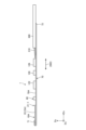
- FIG. 1 is a schematic diagram showing an example of the external appearance of a detection device according to a first embodiment when a finger is placed inside the detection device as viewed from the side of a housing.
- FIG. 2 is a schematic cross-sectional view taken along line AA of FIG.
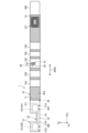
- FIG. 3 is a development view showing an example of the front surface side of the substrate and the flexible printed circuit board shown in FIG.
- FIG. 4 is a development view showing an example of the rear surface side of the substrate and the flexible printed circuit board shown in FIG.
- FIG. 5 is a development view showing a state in which the flexible printed circuit board shown in FIG. 4 is bent.
- FIG. 6 is a side view of the substrate and the flexible printed circuit board shown in FIG. FIG.
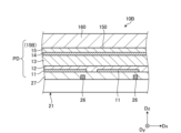
- FIG. 7 is a schematic cross-sectional view showing an example of a laminated structure of the optical sensor taken along the line BB shown in FIG.
- FIG. 8 is a schematic cross-sectional view showing an example of a laminated structure of the optical sensor taken along the line CC shown in FIG.
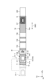
- FIG. 9 is a development view showing an example of the front surface side of the substrate and the flexible printed circuit board according to the second embodiment.
- FIG. 10 is a development view showing an example of the rear surface side of the substrate and the flexible printed circuit board according to the second embodiment.
- FIG. 11 is a development view showing a state in which the flexible printed circuit board shown in FIG. 10 is bent.
- 12 is a side view of the substrate and the flexible printed circuit board shown in FIG. 11.
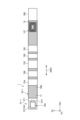
- FIG. 13 is a development view showing an example of the front surface side of the substrate and the flexible printed circuit board according to the third embodiment.
- FIG. 14 is a development view showing an example of the rear surface side of the substrate and the flexible printed circuit board according to the third embodiment.
- FIG. 15 is a development view showing a state in which the flexible printed circuit board shown in FIG. 14 is bent.
- 16 is a side view of the substrate and the flexible printed circuit board shown in FIG. 15.
- the term "on top” is used, unless otherwise specified, to include both a case in which another structure is placed directly on top of a structure so as to be in contact with the structure, and a case in which another structure is placed above a structure via yet another structure.
- FIG. 1 is a schematic diagram showing an example of the appearance of the detection device according to the first embodiment when a finger is placed inside the detection device when viewed from the side of the housing.
- FIG. 2 is a schematic cross-sectional view of the A-A cross section shown in FIG. 1.
- FIG. 3 is a development view showing an example of the front side of the substrate and the flexible printed circuit board shown in FIG. 1.
- FIG. 4 is a development view showing an example of the back side of the substrate and the flexible printed circuit board shown in FIG. 1.
- FIG. 5 is a development view showing a state in which the flexible printed circuit board shown in FIG. 4 is folded.
- FIG. 6 is a side view of the substrate and the flexible printed circuit board shown in FIG. 5.
- FIG. 5 is a development view showing a state in which the flexible printed circuit board shown in FIG. 4.
- FIG. 7 is a schematic cross-sectional view showing an example of the stacked configuration of the optical sensor in the B-B cross section shown in FIG. 3.
- FIG. 8 is a schematic cross-sectional view showing an example of the stacked configuration of the optical sensor in the C-C cross section shown in FIG. 3.
- the detection device 1 shown in FIG. 1 is a ring-shaped device that can be attached and detached to the human body, and is worn on a finger Fg of the human body.
- the finger Fg includes the thumb, index finger, middle finger, ring finger, little finger, etc.
- the human body is the person to be authenticated, whose identity is verified by the detection device 1.
- the detection device 1 can detect biometric information about a living body from the finger Fg on which it is worn.
- the finger Fg is an example of a measurement target.
- the measurement target is a living body or a part of a living body, and is the measurement target.
- the detection device 1 is made into a ring or wristband, making it easy for the user to carry. In the following description, it is assumed that the detection device 1 is used as a ring.
- the detection device 1 includes a housing 200, a substrate 21, a light source 60, a first optical sensor 10A, a second optical sensor 10B, and a flexible printed circuit board 70.
- the detection device 1 includes a battery 300 connected to the flexible printed circuit board 70 inside the housing 200, and is a device that operates using the power of the battery 300.
- the substrate 21 and the flexible printed circuit board 70 are electrically connected.
- the housing 200 is formed in a ring shape (annular shape) that can be attached to the finger Fg, and is a wearing member that is attached to a living body.
- the housing 200 includes a first housing 210 and a second housing 220.
- the housing 200 is formed in a ring shape by integrating the first housing 210 and the second housing 220.
- the first housing 210 is a member that comes into contact with the human body on which the housing 200 is attached.
- the first housing 210 houses the light source 60, the first optical sensor 10A, the second optical sensor 10B, etc. inside.
- the first housing 210 is formed in a ring shape from a housing material such as, for example, a transparent synthetic resin or silicone.
- the first housing 210 has a light irradiation unit 60R that protrudes inward, and is configured to be able to irradiate light from the light source 60 from the light irradiation unit 60R to the finger Fg.
- the light irradiation unit 60R is, for example, a translucent convex lens.
- the second housing 220 has a surface of the housing 200 that covers part of the outer peripheral surface 210A of the first housing 210.
- the second housing 220 is formed in a ring shape from a material such as metal or non-transparent synthetic resin.
- the second housing 220 is provided on the top surface of the first housing 210, i.e., the surface positioned on the surface of the finger Fg on the back of the hand, but it may be configured to cover the entire top surface of the first housing 210.
- the housing 200 accommodates the flexible printed circuit board 70 on which the light source 60, the first optical sensor 10A, the second optical sensor 10B, etc. are mounted, and the battery 300 inside the first housing 210.
- the flexible printed circuit board 70 is accommodated inside the first housing 210 with the first end 71 folded at the folding portion 73.
- the board 21 on which the first optical sensor 10A and the second optical sensor 10B are mounted is connected to the first end 71 of the folding portion 73.
- the flexible printed circuit board 70 is accommodated inside the housing 200 by, for example, forming the housing 200 in a ring shape in a mold and filling the surrounding area with a filling material.
- the detection device 1 is disposed inside the housing 200, inside the flexible printed circuit board 70, so that the first optical sensor 10A and the second optical sensor 10B can receive light from the finger Fg.
- the flexible printed circuit board 70 extends from the first end 71 to the second end 72 and is formed in a deformable band shape.
- the flexible printed circuit board 70 has mounting areas 73A, 73B, 73C, 73D, and 73E provided between the first end 71 and the second end 72.
- the light source 60 is mounted in the mounting area 73C located in the center of the mounting areas 73A, 73B, 73C, 73D, and 73E, and the other areas are unmounted.
- the first surface 70A of the flexible printed circuit board 70 is the surface on which the light source 60 is mounted
- the second surface 70B is the surface on which the light source 60 is not mounted.
- the electronic components include, for example, a control circuit 122 in the mounting area 73A, a detection circuit 123 in the mounting area 73B, a control circuit 124 in the mounting area 73C, a control circuit 125 in the mounting area 73D, and a power supply circuit 126 in the mounting area 73E.
- the flexible printed circuit board 70 has a substrate 21 having a cutout portion 22 shown in FIG. 3 and FIG. 4 mounted so as to straddle the vicinity of the light source 60 in the mounting area 73C.
- the substrate 21 is a substrate on which the first optical sensor 10A, the second optical sensor 10B, etc. are mounted on the surface 21H.
- the flexible printed circuit board 70 electrically connects the light source 60, the first optical sensor 10A, the second optical sensor 10B, etc., to the electronic device.
- the substrate 21 is connected to the first end portion 71 of the flexible printed circuit board 70 so that the surface 21H on which the first optical sensor 10A, the second optical sensor 10B, etc. are mounted is a surface continuous with the second surface 70B of the flexible printed circuit board 70.
- the first optical sensor 10A and the second optical sensor 10B are arranged to sandwich the light source 60 in the circumferential direction 200C. That is, the detection device 1 is arranged in the circumferential direction 200C with the first optical sensor 10A, the light source 60, and the second optical sensor 10B lined up in that order.
- the first optical sensor 10A and the second optical sensor 10B are arranged to sandwich the light source 60 in the circumferential direction 200C, so that the light emitted by the light source 60 can be detected around the light source 60.
- the detection device 1 further includes a substrate 21 and a terminal portion 40.
- the substrate 21 is an insulating substrate, and is formed in a strip shape, for example, from a film-like resin.
- the first optical sensor 10A and the second optical sensor 10B are mounted on the surface 21H of the substrate 21, making it a deformable substrate.
- the terminal portion 40 is provided at one end 21A of the surface 21H of the substrate 21.
- the substrate 21 is electrically connected to the flexible printed circuit board 70 by being attached to the flexible printed circuit board 70 via the terminal portion 40. That is, in a plan view, the back surface 21R of the substrate 21 is a surface that is continuous with the first surface 70A of the flexible printed circuit board 70.
- the flexible printed circuit board 70 has a battery charging coil 127 provided at the second end 72.
- the battery charging coil 127 is formed by winding a conductor inside the flexible printed circuit board 70.
- the first direction Dx is a direction in a plane parallel to the substrate 21 and the flexible printed circuit board 70, and is the same direction as the circumferential direction 200C.
- the second direction Dy is a direction in a plane parallel to the substrate 21, and is a direction perpendicular to the first direction Dx.
- the second direction Dy may intersect with the first direction Dx without being perpendicular thereto.
- the third direction Dz is a direction perpendicular to the first direction Dx and the second direction Dy.
- the third direction Dz is the normal direction of the substrate 21.
- plane view refers to the positional relationship when viewed from a direction perpendicular to the substrate 21.
- the battery 300 is a film-type lithium ion battery and is bendable.
- the battery 300 is electrically connected to the power supply circuit 126 in the mounting area 73E of the second surface 70B of the flexible printed circuit board 70 via a connection portion 310.
- the width of the battery 300 in the first direction Dx is equal to or smaller than the width of the flexible printed circuit board 70 in the second direction Dy, and the length of the battery 300 in the first direction Dx is smaller than the length of the flexible printed circuit board 70 in the first direction Dx. This allows the detection device 1 to be mounted on the flexible printed circuit board 70 so that the battery 300 does not protrude from the flexible printed circuit board 70.
- the first end 71 of the flexible printed circuit board 70 is folded at the folding portion 73, so that the first optical sensor 10A and the second optical sensor 10B are positioned on either side of the light source 60 in the circumferential direction 200C of the housing 200.
- the substrate 21 has a cutout portion 22 between both ends in the circumferential direction 200C of the housing 200, i.e., in the first direction Dx (longitudinal direction) of the substrate 21.
- the first optical sensor 10A is positioned on one end 21A side of the cutout portion 22, and the second optical sensor 10B is positioned on the other end 21B side of the substrate 21.
- the flexible printed circuit board 70 is folded at the folding portion 73, so that the cutout portion 22 of the substrate 21 is positioned so that it overlaps with the light source 60.
- the cutout portion 22 is arranged in a position overlapping the light source 60 means that the light source 60 is attached to the flexible printed circuit board 70 with the light source 60 positioned in the area of the cutout portion 22 of the substrate 21.
- the substrate 21 may be fixed to the flexible printed circuit board 70 by an adhesive member, or may not be fixed to the flexible printed circuit board 70.
- the terminal section 40 is a member for electrically connecting the first optical sensor 10A and the second optical sensor 10B of the substrate 21 to the control circuit 122 and the power supply circuit 126 of the flexible printed circuit board 70.
- the terminal section 40 supplies a power signal (electricity) from the power supply circuit 126 to the first optical sensor 10A and the second optical sensor 10B via wiring.
- the terminal section 40 has multiple terminals (not shown) and is configured to be electrically connectable to multiple wirings.
- the terminal portion 40 is provided at one end 21A of the substrate 21 in the first direction Dx. As shown in FIG. 4, the terminal portion 40 is connected to a connection portion (not shown) at a first end 71 of the first surface 70A of the flexible printed circuit board 70. When the electrically connected flexible printed circuit board 70 is folded at the folding portion 73, the terminal portion 40 is sandwiched between the first surfaces 70A of the flexible printed circuit board 70 as shown in FIG. 6, and is housed inside the housing 200 in this state. The terminal portion 40 supplies power from the power supply circuit 126 to the first optical sensor 10A and the second optical sensor 10B.
- the flexible printed circuit board 70 is housed inside the housing 200 so that the first surface 70A on which the first optical sensor 10A, the second optical sensor 10B, and the light source 60 are mounted faces the inner peripheral surface 200B of the housing 200. If the flexible printed circuit board 70 is translucent, the first optical sensor 10A, the second optical sensor 10B, and the light source 60 may be mounted on the second surface 70B opposite the first surface 70A. In this case, the light source 60 may be positioned so that it emits light toward the flexible printed circuit board 70 and the light that has passed through the flexible printed circuit board 70 is emitted toward the outside of the housing 200.
- the light source 60 is provided inside the first housing 210 of the housing 200, and is configured to be able to irradiate light toward the finger Fg wearing the housing 200.
- an inorganic LED Light Emitting Diode
- an organic EL Organic Light Emitting Diode
- the light source 60 irradiates light of a predetermined wavelength.
- the light source 60 has a first light source 61 that irradiates red light, a second light source 62 that irradiates near-infrared light, and a second light source 63 that irradiates green light.
- the light emitted from the light source 60 is reflected by the surface of the object to be detected, such as a finger Fg, and enters the first optical sensor 10A and the second optical sensor 10B.
- the light emitted from the light source 60 may be reflected inside the finger Fg or pass through the finger Fg and enter the first optical sensor 10A and the second optical sensor 10B.
- Information about a living body includes, for example, the pulse wave, pulse, and blood vessel image of the finger or palm.
- the detection device 1 may be configured as a fingerprint detection device that detects fingerprints, or a vein detection device that detects blood vessel patterns such as veins.
- Each of the first optical sensor 10A and the second optical sensor 10B detects light emitted by the light source 60 and reflected by the finger Fg, etc., light that is directly incident, etc.
- the first optical sensor 10A and the second optical sensor 10B are organic photodiodes (OPDs).
- the first optical sensor 10A is provided on the housing 200 so as to be adjacent to one end of the light source 60 in the circumferential direction 200C of the housing 200.
- the second optical sensor 10B is provided on the housing 200 so as to be adjacent to the other end of the light source 60 in the circumferential direction 200C of the housing 200.
- the first optical sensor 10A has a substrate 21 and a photodiode PD.
- the first optical sensor 10A further has wiring 26 and an insulating layer 27.
- wiring 26 is provided on the upper surface.
- the wiring 26 is a shield layer, and is formed, for example, of a metal wiring, and is formed of a material having better conductivity than the lower electrode 11 of the photodiode PD.
- the wiring 26 is provided in a layer between the substrate 21 and the photodiode PD in the third direction Dz.
- the wiring 26 is electrically connected to the terminal portion 40 in the substrate 21.
- the wiring 26 may be formed, for example, in the same layer as the lower electrode 11, or may be formed of metal.
- the insulating layer 27 is provided on the substrate 21, covering the wiring 26.
- the insulating layer 27 may be an inorganic insulating film or an organic insulating film.
- the photodiode PD is provided on the insulating layer 27.
- the photodiode PD has a lower electrode 11, a lower buffer layer 12, an active layer 13, an upper buffer layer 14, and an upper electrode 15 (upper electrode 15A).
- the photodiode PD is stacked in the following order in the third direction Dz perpendicular to the substrate 21: the lower electrode 11, the lower buffer layer 12 (hole transport layer), the active layer 13, the upper buffer layer 14 (electron transport layer), and the upper electrode 15A.
- the lower electrode 11 is the anode electrode of the photodiode PD and is formed of a conductive material having light transmission, such as ITO (Indium Tin Oxide).
- ITO Indium Tin Oxide
- the characteristics (e.g., voltage-current characteristics and resistance value) of the active layer 13 change depending on the light irradiated thereto.
- An organic material is used as the material of the active layer 13.
- the active layer 13 is a bulk heterostructure in which a p-type organic semiconductor and an n-type fullerene derivative (PCBM), which is an n-type organic semiconductor, are mixed.
- PCBM n-type fullerene derivative
- low molecular weight organic materials such as C60 (fullerene), PCBM (phenyl C61-butyric acid methyl ester), CuPc (copper phthalocyanine), F16CuPc (fluorinated copper phthalocyanine), rubrene (5,6,11,12-tetraphenyltetracene), and PDI (perylene derivative) can be used as the active layer 13.
- C60 fulllerene
- PCBM phenyl C61-butyric acid methyl ester
- CuPc copper phthalocyanine
- F16CuPc fluorinated copper phthalocyanine
- rubrene 5,6,11,12-tetraphenyltetracene
- PDI perylene derivative
- the active layer 13 can be formed by a deposition type (dry process) using these low molecular weight organic materials.
- the active layer 13 may be, for example, a laminated film of CuPc and F16CuPc, or a laminated film of rubrene and C60.
- the active layer 13 can also be formed by a coating type (wet process).
- the active layer 13 is made of a material that combines the above-mentioned low molecular weight organic material and a polymer organic material.
- the polymer organic material for example, P3HT (poly(3-hexylthiophene)), F8BT (F8-alt-benzothiadiazole), etc. can be used.
- the active layer 13 can be a film in which P3HT and PCBM are mixed, or a film in which F8BT and PDI are mixed.
- the lower buffer layer 12 is a hole transport layer.
- the upper buffer layer 14 is an electron transport layer.
- the lower buffer layer 12 and the upper buffer layer 14 are provided to facilitate the holes and electrons generated in the active layer 13 to reach the lower electrode 11 or the upper electrode 15.
- the lower buffer layer 12 (hole transport layer) is directly on top of the lower electrode 11 and is also provided in the region between adjacent lower electrodes 11.
- the active layer 13 is directly on top of the lower buffer layer 12.
- the material of the hole transport layer is a metal oxide layer. Tungsten oxide (WO 3 ), molybdenum oxide, or the like is used as the metal oxide layer.
- the upper buffer layer 14 (electron transport layer) is in direct contact with the active layer 13, and the upper electrode 15 is in direct contact with the upper buffer layer 14.
- the material used for the electron transport layer is ethoxylated polyethyleneimine (PEIE).
- the materials and manufacturing methods of the lower buffer layer 12, active layer 13, and upper buffer layer 14 are merely examples, and other materials and manufacturing methods may be used.
- the lower buffer layer 12 and upper buffer layer 14 are not limited to single-layer films, and may be formed as laminated films including an electron blocking layer and a hole blocking layer.
- the upper electrode 15 is provided on the upper buffer layer 14.
- the upper electrode 15 is a cathode electrode of the photodiode PD, and is formed continuously over the entire first optical sensor 10A and the second optical sensor 10B. In other words, the upper electrode 15 is provided continuously over the multiple photodiodes PD.
- the upper electrode 15 faces the multiple lower electrodes 11, sandwiching the lower buffer layer 12, the active layer 13, and the upper buffer layer 14.
- the upper electrode 15 is formed of a conductive material having translucency, such as ITO or IZO. A part of the end of the upper surface 150 of the upper electrode 15 is electrically connected to the conductive material 24, and is electrically connected to the power electrode 211 through the conductive material 24.
- the power electrode 211 is electrically connected to the battery 300, and is configured to be able to supply power from the battery 300.
- a sealing film 160 is provided on the upper electrode 15, etc.
- the sealing film 160 is an inorganic film such as a silicon nitride film or an aluminum oxide film, or a resin film such as acrylic.
- the sealing film 160 is not limited to a single layer, and may be a laminated film of two or more layers combining the inorganic film and the resin film.
- the photodiode PD is well sealed by the sealing film 160, and the intrusion of moisture from the upper surface side can be suppressed.
- the second optical sensor 10B has the lower electrode 11 of the second optical sensor 10B in a region of the substrate 21 different from the lower electrode 11 of the first optical sensor 10A.
- the lower electrode 11 is covered with the lower buffer layer 12, the active layer 13, the upper buffer layer 14, and the upper electrode 15 (upper electrode 15B).
- the second optical sensor 10B has the substrate 21, the photodiode PD, the wiring 26, and the insulating layer 27.
- the photodiode PD, the wiring 26, and the insulating layer 27 have the same configuration as the photodiode PD, the wiring 26, and the insulating layer 27 of the first optical sensor 10A described above.
- the photodiode PD of the second optical sensor 10B has the lower electrode 11, the lower buffer layer 12, the active layer 13, the upper buffer layer 14, and the upper electrode 15B.
- a sealing film 160 is provided on the upper electrode 15B, etc., so that the photodiode PD is well sealed.
- the substrate 21 has the areas of the first optical sensor 10A and the second optical sensor 10B, and is a single, integrally formed common substrate.
- the substrate 21 has a cutout portion 22 formed between the area of the first optical sensor 10A and the area of the second optical sensor 10B in the first direction Dx.
- the substrate 21 has the cutout portion 22 between the first optical sensor 10A and the second optical sensor 10B, and a connecting portion 23 that is in contact with the cutout portion 22 and is between the first optical sensor 10A and the second optical sensor 10B.
- the cutout portion 22 is formed in the first direction Dx at a distance longer than the length of the light source 60.
- the cutout portion 22 is formed in the second direction Dy at a distance longer than the length of the light source 60 and shorter than the length (width) of the substrate 21.
- the substrate 21 is integrally formed by connecting the first optical sensor 10A and the second optical sensor 10B with the connecting portion 23 along the cutout portion 22.
- the connecting portion 23 includes the lower buffer layer 12, the active layer 13, the upper buffer layer 14, and the electrode connecting portion 151 of the upper electrode 15. As a result, the connecting portion 23 integrally forms the upper electrodes 15A and 15B of the first optical sensor 10A and the second optical sensor 10B.
- the first optical sensor 10A and the second optical sensor 10B are connected by the connecting portion 23 and are operated by power supplied from the power supply electrode 211 to the common upper electrode 15.
- the cutout portion 22 is formed in a shape in which the light source 60 can be placed.
- the cutout portion 22 is formed in a substantially rectangular shape in a plan view, but may be, for example, a semicircular, triangular, polygonal, or other shape.
- the cutout portion 22 may be a through hole through which light from the light source 60 can pass.
- the electrode connection portion 151 is provided on the connection portion 23 of the substrate 21 so as to be stacked on the upper buffer layer 14, the active layer 13, and the lower buffer layer 12.
- the multiple wirings 26 of the substrate 21 are connected to the control circuit 122 via multiple signal lines (not shown) of the flexible printed circuit board 70.
- the control circuit 122 is electrically connected to the lower electrodes 11 of the first optical sensor 10A and the second optical sensor 10B via multiple signal lines.
- the control circuit 122 is a circuit that supplies control signals to the multiple photodiodes PD to control the detection operation.
- the multiple photodiodes PD each output an electrical signal corresponding to the light irradiated thereon as a detection signal Vdet to the detection circuit 123.
- the detection circuit 123 is a detection circuit for the detection signal Vdet.
- the detection circuit 123 is, for example, an analog front-end circuit (AFE).
- AFE analog front-end circuit
- the detection circuit 123 is a signal processing circuit that has at least the functions of a detection signal amplifier circuit and an A/D conversion circuit.
- the detection signal amplifier circuit amplifies the detection signal Vdet.
- the A/D conversion circuit converts the analog signal output from the detection signal amplifier circuit into a digital signal.
- the charging control circuit 124 controls the power of wireless power transmission, in which electrical energy reaches the battery charging coil 127 from the outside by electromagnetic means.
- the coupling method for wireless power transmission is selected from among electromagnetic induction, electromagnetic resonance, radio wave, etc.
- the control circuit 124 charges the battery 300 using the wirelessly transmitted power.
- the control circuit 125 supplies a control signal to the light source 60 to control whether the light source 60 is turned on or off.
- the power supply circuit 126 supplies a power supply signal (power) from the battery 300 to the first optical sensor 10A and the second optical sensor 10B via the terminal unit 40.
- the flexible printed circuit board 70 has the light source 60 mounted on the first surface 70A, and the control circuit 122, the detection circuit 123, the control circuit 124, the control circuit 125, and the power supply circuit 126 mounted on the second surface 70B.
- the first optical sensor 10A and the second optical sensor 10B are formed on the board 21, and the terminal portion 40 is mounted on the board 21.
- the board 21 is connected to the first end portion 71 of the flexible printed circuit board 70 by connecting the connection portion of the first surface 70A of the flexible printed circuit board 70 to the terminal portion 40.
- the flexible printed circuit board 70 is folded at the folding portion 73, and the other end portion 21B of the board 21 is brought close to the first surface 70A of the flexible printed circuit board 70, and the board 21 is disposed on the first surface 70A of the flexible printed circuit board 70 so that the notch portion 22 of the board 21 overlaps with the light source 60.
- the battery 300 is electrically connected to the flexible printed circuit board 70 at a second end 72.
- the substrate 21, the flexible printed circuit board 70, and the battery 300 are housed in a mold in a ring-shaped state, and a filling material is filled around them to form the housing 200, so that the substrate 21, the flexible printed circuit board 70, and the battery 300 are housed inside the housing 200.
- the detection device 1 is formed as a device in which the flexible printed circuit board 70 is folded and the substrate 21, the flexible printed circuit board 70, and the battery 300 are housed in the housing 200, with the cutout portion 22 being arranged at a position where it overlaps with the light source 60, as shown in FIG.
- the detection device 1 is in a state where the inner circumferential surface 210B of the first housing 210 of the housing 200 is in contact with or close to the finger Fg.
- the detection device 1 operates the first optical sensor 10A and the second optical sensor 10B by supplying power from the battery 300 to the common upper electrode 15 via the terminal portion 40.
- the detection device 1 turns on the light source 60, causing the light source 60 to irradiate light toward the finger Fg.
- the light source 60 irradiates light to one side and the other side in the circumferential direction 200C.
- the detection device 1 receives light reflected by the finger Fg or the like with the first optical sensor 10A and the second optical sensor 10B.
- the detection device 1 detects information about the living body of the finger Fg based on the amount of light received detected by each of the two photodiodes PD of the first optical sensor 10A and the second optical sensor 10B.
- the substrate 21 having the first optical sensor 10A and the second optical sensor 10B is connected to the flexible printed circuit board 70 via the terminal portion 40, and the flexible printed circuit board 70 is bent so that the cutout portion 22 of the substrate 21 is positioned to overlap the light source 60 of the flexible printed circuit board 70.
- the detection device 1 can bend the flexible printed circuit board 70 in the connection direction to position the substrate 21, thereby reducing the storage space.
- the detection device 1 can prevent the components that connect and store the substrate 21 having the multiple optical sensors and the flexible printed circuit board 70 having the light source 60 from becoming large.
- the lower buffer layer 12, active layer 13, upper buffer layer 14, and upper electrode 15 of the first optical sensor 10A and the second optical sensor 10B can be common. This allows the detection device 1 to supply power to the integrated upper electrode 15 for the first optical sensor 10A and the second optical sensor 10B, simplifying the configuration of the substrate 21. As a result, even if multiple optical sensors are arranged on the substrate 21, the detection device 1 can prevent the substrate 21 from becoming large.
- the detection device 1 has multiple electronic components mounted on the second surface 70B of the flexible printed circuit board 70 opposite the light source 60. This simplifies the configuration of the flexible printed circuit board 70 and further reduces the storage space required by mounting multiple electronic components on the second surface 70B of the flexible printed circuit board 70 and mounting the light source 60 on the opposite first surface 70A.
- the substrate 21 and the flexible printed circuit board 70 are housed in a ring-shaped housing 200. This allows the detection device 1 to detect the light emitted by the light source 60 with high accuracy over a wide range of the housing 200 using multiple optical sensors, without increasing the size of the ring-shaped housing 200.
- Fig. 9 is a development view showing an example of a front surface side of a substrate and a flexible printed circuit board according to embodiment 2.
- Fig. 10 is a development view showing an example of a back surface side of a substrate and a flexible printed circuit board according to embodiment 2.
- Fig. 11 is a development view showing a state in which the flexible printed circuit board shown in Fig. 10 is folded.
- Fig. 12 is a side view of the substrate and the flexible printed circuit board shown in Fig. 11.
- the detection device 1 includes the housing 200, the terminal section 40, the light source 60, the first optical sensor 10A, the flexible printed circuit board 70, and the board 21-1.
- the detection device 1 includes a battery 300 connected to the flexible printed circuit board 70 inside the housing 200, and is a device that operates using the power of the battery 300.
- the flexible printed circuit board 70 has multiple electronic components mounted thereon.
- the electronic components include the control circuit 122 in the mounting area 73A, the detection circuit 123 in the mounting area 73B, the control circuit 124 in the mounting area 73C, the control circuit 125 in the mounting area 73D, and the power supply circuit 126 in the mounting area 73E.
- the detection device 1 includes the terminal section 40, the light source 60, the first optical sensor 10A, the flexible printed circuit board 70, and the board 21-1 housed in the ring-shaped housing 200.
- the substrate 21-1 is an insulating substrate, and is formed in a band shape, for example, from a film-like resin.
- the first optical sensor 10A is mounted on the surface 21H of the substrate 21-1 near the other end 21B, making the substrate 21-1 deformable.
- the terminal portion 40 is provided on one end 21A of the surface 21H of the substrate 21-1.
- the substrate 21-1 is attached to the flexible printed circuit board 70 via the terminal portion 40, and is thereby electrically connected to the flexible printed circuit board 70. That is, in a plan view, the rear surface 21R of the substrate 21-1 is a surface that is continuous with the first surface 70A of the flexible printed circuit board 70.
- flexible printed circuit board 70 differs from embodiment 1 in that on the first surface 70A, light source 60 is mounted in mounting area 73B based on the length of board 21, the length of the bent portion, etc., rather than in mounting area 73C.
- flexible printed circuit board 70 moves the position of light source 60 toward first end 71 due to a change in the length of board 21 in the first direction Dx (circumferential direction 200C).
- the substrate 21-1 shown in Figures 9 and 10 positions the first optical sensor 10A adjacent to the light source 60 in the circumferential direction 200C of the housing 200 by folding the first end 71 of the flexible printed circuit board 70 at the folding portion 73. As shown in Figure 11, the substrate 21-1 is positioned near the light source 60 by folding the flexible printed circuit board 70 at the folding portion 73.
- the substrate 21-1 shown in Figure 12 may be fixed to the flexible printed circuit board 70 by an adhesive member, or may not be fixed to the flexible printed circuit board 70.
- the terminal section 40 shown in FIG. 10 is a member for electrically connecting the first optical sensor 10A on the substrate 21 to the control circuit 122 and power supply circuit 126 on the flexible printed circuit board 70.
- the terminal section 40 supplies a power signal (electricity) from the power supply circuit 126 to the first optical sensor 10A via wiring.
- the terminal section 40 has multiple terminals (not shown) and is configured to be electrically connectable to multiple wirings.
- the flexible printed circuit board 70 shown in FIG. 12 is housed inside the housing 200 so that the first surface 70A on which the first optical sensor 10A and the light source 60 are mounted faces the inner peripheral surface 200B of the housing 200. If the flexible printed circuit board 70 is translucent, the first optical sensor 10A and the light source 60 may be mounted on the second surface 70B opposite the first surface 70A. In this case, the light source 60 may be positioned so that it emits light toward the flexible printed circuit board 70 and the light that has passed through the flexible printed circuit board 70 is emitted toward the outside of the housing 200.
- the light emitted from the light source 60 is reflected by the surface of the object to be detected, such as a finger Fg, and enters the first optical sensor 10A.
- the light emitted from the light source 60 may be reflected inside the finger Fg or pass through the finger Fg and enter the first optical sensor 10A.
- Information about a living body includes, for example, the pulse wave, pulse, and blood vessel image of the finger or palm.
- the detection device 1 may be configured as a fingerprint detection device that detects fingerprints, or a vein detection device that detects blood vessel patterns such as veins.
- the first optical sensor 10A detects light emitted by the light source 60 and reflected by the finger Fg, etc., and light that is directly incident.
- the first optical sensor 10A is an organic photodiode (OPD).
- OPD organic photodiode
- the first optical sensor 10A is provided on the housing 200 so as to be adjacent to one end of the light source 60 in the circumferential direction 200C of the housing 200.
- a configuration example of the detection device 1 according to the second embodiment has been described above. Note that the above configuration described using Figs. 9 to 12 is merely an example, and the configuration of the detection device 1 according to the second embodiment is not limited to this example. The configuration of the detection device 1 according to the second embodiment can be flexibly modified according to the specifications and operation.
- the flexible printed circuit board 70 has the light source 60 mounted on the first surface 70A, and the control circuit 122, the detection circuit 123, the control circuit 124, the control circuit 125, and the power supply circuit 126 mounted on the second surface 70B.
- the first optical sensor 10A is formed on the board 21-1, and the terminal section 40 is mounted on the board 21-1.
- the board 21-1 is connected to the first end 71 of the flexible printed circuit board 70 by connecting the connection section of the first surface 70A of the flexible printed circuit board 70 to the terminal section 40.
- the flexible printed circuit board 70 is folded at the folding section 73, and the other end 21B of the board 21-1 is brought closer to the light source 60, while the first optical sensor 10A of the board 21-1 is disposed on the first surface 70A of the flexible printed circuit board 70 so that the first optical sensor 10A of the board 21-1 is adjacent to the light source 60.
- the substrate 21-1 is disposed so as to cover the mounting area 73A on the first surface 70A of the flexible printed circuit board 70 and have the other end 21B adjacent to the light source 60.
- the flexible printed circuit board 70 is electrically connected to the battery 300 at a second end 72.
- the substrate 21-1, the flexible printed circuit board 70, and the battery 300 are housed in a mold in a ring-shaped state, and a filling material is filled around the substrate 21-1 to form the housing 200, thereby being housed inside the housing 200.
- the detection device 1 is formed as a device in which the flexible printed circuit board 70 is folded and the substrate 21-1, the flexible printed circuit board 70, and the battery 300 are housed in the housing 200, in which the first optical sensor 10A is disposed at a position adjacent to the light source 60.
- the detection device 1 In the detection device 1, the inner circumferential surface 210B of the first housing 210 of the housing 200 is in contact with or close to the finger Fg.
- the detection device 1 operates the first optical sensor 10A by supplying power from the battery 300 to the upper electrode 15 of the first optical sensor 10A via the terminal portion 40.
- the detection device 1 turns on the light source 60, causing the light source 60 to irradiate light toward the finger Fg.
- the light source 60 irradiates light to one side and the other side in the circumferential direction 200C.
- the detection device 1 receives light reflected by the finger Fg or the like with the first optical sensor 10A.
- the detection device 1 detects information about the living body of the finger Fg based on the amount of light received detected by each of the photodiodes PD of the first optical sensor 10A.
- the detection device 1 the substrate 21-1 having the first optical sensor 10A and the flexible printed circuit board 70 are connected via the terminal portion 40, and the flexible printed circuit board 70 is bent so that the first optical sensor 10A of the substrate 21-1 is disposed adjacent to the light source 60 of the flexible printed circuit board 70.
- the detection device 1 can reduce the storage space by bending the flexible printed circuit board 70 and arranging the substrate 21-1.
- the detection device 1 makes it easy to mount multiple electronic components on the flexible printed circuit board 70, and can improve the freedom of arrangement of the first optical sensor 10A and the light source 60.
- the detection device 1 can accommodate the first optical sensor 10A and the light source 60 in a state of being adjacent to each other without increasing the size of the housing 200 that accommodates them.
- FIG. 13 is a development view showing an example of a front surface side of a substrate and a flexible printed circuit board according to embodiment 3.
- Fig. 14 is a development view showing an example of a back surface side of a substrate and a flexible printed circuit board according to embodiment 3.
- Fig. 15 is a development view showing a state in which the flexible printed circuit board shown in Fig. 14 is folded.
- Fig. 16 is a side view of the substrate and the flexible printed circuit board shown in Fig. 15.
- the detection device 1 includes the housing 200, the board 21-1, the terminal portion 40, the light source 60, the first optical sensor 10A, and the flexible printed circuit board 70.
- the detection device 1 includes a battery 300 connected to the flexible printed circuit board 70 inside the housing 200, and is a device that operates using the power of the battery 300.
- the first optical sensor 10A and the board 21-1 have the same configuration as the first optical sensor 10A and the board 21-1 in the second embodiment.
- the flexible printed circuit board 70 has multiple electronic components mounted thereon. The electronic components include the control circuit 122, the power supply circuit 126, and the control circuit 128 described above.
- the detection device 1 includes the terminal portion 40, the light source 60, the first optical sensor 10A, the flexible printed circuit board 70, and the board 21-1 housed in the ring-shaped housing 200.
- the flexible printed circuit board 70 has the control circuit 122, power supply circuit 126, and control circuit 128 mounted on the first surface 70A on which the light source 60 is mounted, and no electronic components mounted on the second surface 70B.
- the control circuit 128 includes a single circuit that combines the detection circuit 123, the control circuit 124, and the control circuit 125 described above.
- the substrate 21-1 shown in FIGS. 13 and 14 has a first end 71 of the flexible printed circuit board 70 folded at a folding portion 73, thereby positioning the first optical sensor 10A adjacent to the light source 60 in the circumferential direction 200C of the housing 200 while bringing the other end 21B of the substrate 21-1 closer to the light source 60.
- the substrate 21-1 is positioned near the light source 60 by folding the flexible printed circuit board 70 at the folding portion 73.
- the substrate 21-1 shown in FIG. 16 may or may not be fixed to the flexible printed circuit board 70 by an adhesive member.
- the flexible printed circuit board 70 is translucent, it may be mounted on the second surface 70B opposite the first surface 70A on which the first optical sensor 10A, the light source 60, and the electronic components are mounted.
- the light source 60 may be positioned so that it emits light toward the flexible printed circuit board 70 and the light that has passed through the flexible printed circuit board 70 is emitted toward the outside of the housing 200.
- the light emitted from the light source 60 is reflected by the surface of the object to be detected, such as a finger Fg, and enters the first optical sensor 10A.
- the light emitted from the light source 60 may be reflected inside the finger Fg or pass through the finger Fg and enter the first optical sensor 10A.
- Information about a living body includes, for example, the pulse wave, pulse, and blood vessel image of the finger or palm.
- the detection device 1 may be configured as a fingerprint detection device that detects fingerprints, or a vein detection device that detects blood vessel patterns such as veins.
- the above describes an example configuration of the detection device 1 according to the third embodiment. Note that the above configuration described using Figs. 13 to 16 is merely an example, and the configuration of the detection device 1 according to the third embodiment is not limited to this example.
- the configuration of the detection device 1 according to the third embodiment can be flexibly modified according to the specifications and operation.
- the flexible printed circuit board 70 has the light source 60, the control circuit 122, the control circuit 128, and the power supply circuit 126 mounted on the first surface 70A.
- the first optical sensor 10A is formed on the board 21-1, and the terminal portion 40 is mounted on the board 21-1.
- the board 21-1 is connected to the first end portion 71 of the flexible printed circuit board 70 by connecting the connection portion of the first surface 70A of the flexible printed circuit board 70 to the terminal portion 40.
- the flexible printed circuit board 70 is folded at the folding portion 73, and the board 21-1 is disposed on the first surface 70A of the flexible printed circuit board 70 so that the first optical sensor 10A of the board 21-1 is adjacent to the light source 60.
- the board 21-1 is disposed so as to cover the mounting area 73A on the first surface 70A of the flexible printed circuit board 70, and the other end portion 21B is adjacent to the light source 60.
- the battery 300 is electrically connected to the flexible printed circuit board 70 at a second end 72.
- the substrate 21-1, the flexible printed circuit board 70, and the battery 300 are housed in a mold in a ring-shaped state, and a filling material is filled around them to form the housing 200, and the substrate 21-1, the flexible printed circuit board 70, and the battery 300 are housed inside the housing 200.
- the detection device 1 is formed as a device in which the flexible printed circuit board 70 is folded and the substrate 21-1, in which the first optical sensor 10A is disposed at a position adjacent to the light source 60, the flexible printed circuit board 70, and the battery 300 are housed in the housing 200.
- the detection device 1 In the detection device 1, the inner circumferential surface 210B of the first housing 210 of the housing 200 is in contact with or close to the finger Fg.
- the detection device 1 operates the first optical sensor 10A by supplying power from the battery 300 to the upper electrode 15 of the first optical sensor 10A via the terminal portion 40.
- the detection device 1 turns on the light source 60, causing the light source 60 to irradiate light toward the finger Fg.
- the light source 60 irradiates light to one side and the other side in the circumferential direction 200C.
- the detection device 1 receives light reflected by the finger Fg or the like with the first optical sensor 10A.
- the detection device 1 detects information about the living body of the finger Fg based on the amount of light received detected by each of the photodiodes PD of the first optical sensor 10A.
- the detection device 1 the substrate 21-1 having the first optical sensor 10A and the flexible printed circuit board 70 are connected via the terminal portion 40, and the flexible printed circuit board 70 is bent so that the first optical sensor 10A of the substrate 21-1 is disposed adjacent to the light source 60 of the flexible printed circuit board 70.
- the detection device 1 can reduce the storage space by bending the flexible printed circuit board 70 and arranging the substrate 21-1.
- the detection device 1 makes it easy to mount multiple electronic components and the light source 60 on the flexible printed circuit board 70, and can improve the freedom of arrangement of the first optical sensor 10A and the light source 60.
- the detection device 1 can accommodate the first optical sensor 10A and the light source 60 in a state of being adjacent to each other without increasing the size of the housing 200 that accommodates them.
- the detection device 1 has multiple electronic components mounted on the first surface 70A of the flexible printed circuit board 70 on which the light source 60 is mounted. This allows the detection device 1 to further simplify the mounting of the flexible printed circuit board 70 by mounting the light source 60 and multiple electronic components on the first surface 70A of the flexible printed circuit board 70.
- the detection device 1 is described as containing the board 21, board 21-1, flexible printed circuit board 70, battery 300, etc. inside the ring-shaped housing 200, but is not limited to this.
- the detection device 1 may be, for example, contained in a rectangular housing, or may be attached to the object to be measured without being contained in a housing.
Landscapes
- Engineering & Computer Science (AREA)
- Health & Medical Sciences (AREA)
- Life Sciences & Earth Sciences (AREA)
- Microelectronics & Electronic Packaging (AREA)
- Physics & Mathematics (AREA)
- Heart & Thoracic Surgery (AREA)
- Public Health (AREA)
- Biophysics (AREA)
- Pathology (AREA)
- Biomedical Technology (AREA)
- Veterinary Medicine (AREA)
- Medical Informatics (AREA)
- Molecular Biology (AREA)
- Surgery (AREA)
- Animal Behavior & Ethology (AREA)
- General Health & Medical Sciences (AREA)
- Spectroscopy & Molecular Physics (AREA)
- Optics & Photonics (AREA)
- Cardiology (AREA)
- Physiology (AREA)
- Structure Of Printed Boards (AREA)
- Measuring Pulse, Heart Rate, Blood Pressure Or Blood Flow (AREA)
Abstract
Description
図1は、実施形態1に係る検出装置の内側に指を収めた状態を筐体の側方から見た場合の外観例を示す模式図である。図2は、図1に示すA-A断面における断面模式図である。図3は、図1に示す基板の表面側及びフレキシブルプリント基板の展開例を示す展開図である。図4は、図1に示す基板の裏面側及びフレキシブルプリント基板の展開例を示す展開図である。図5は、図4に示すフレキシブルプリント基板を折り曲げた状態を示す展開図である。図6は、図5に示す基板及びフレキシブルプリント基板の側面図である。図7は、図3に示すB-B断面における光センサの積層構成例を示す断面模式図である。図8は、図3に示すC-C断面における光センサの積層構成例を示す断面模式図である。
次に、検出装置1の組付け例について説明する。図3及び図4に示すように、フレキシブルプリント基板70は、第1面70Aに光源60が実装され、第2面70Bに制御回路122、検出回路123、制御回路124、制御回路125及び電源回路126が実装される。基板21は、第1光センサ10A及び第2光センサ10Bが形成され、端子部40が実装される。基板21は、フレキシブルプリント基板70の第1面70Aの接続部と端子部40とが接続されることで、フレキシブルプリント基板70の第1端部71に接続される。基板21は、図5に示すように、フレキシブルプリント基板70が折り曲げ部73で折り曲げられ、基板21の他方の端部21Bをフレキシブルプリント基板70の第1面70Aに近付けながら、基板21の切り欠き部22が光源60と重畳するように、フレキシブルプリント基板70の第1面70Aに配置される。フレキシブルプリント基板70は、電池300が第2端部72で電気的に接続される。基板21、フレキシブルプリント基板70及び電池300は、リング状に形成された状態で金型に収容され、その周囲に充填部材を充填されて筐体200が形成されることで、筐体200の内部に収容される。これにより、検出装置1は、図2に示すように、フレキシブルプリント基板70が折り曲げられ、切り欠き部22が光源60と重畳する位置に配置された基板21とフレキシブルプリント基板70と電池300を筐体200に収容した装置として形成される。
次に、指Fgに装着された検出装置1の検出例について説明する。図2に示す一例では、検出装置1は、筐体200の第1筐体210の内周面210Bが指Fgと接触または接近した状態になっている。検出装置1は、端子部40を介して電池300から共通の上部電極15に電力を供給することで、第1光センサ10A及び第2光センサ10Bを動作させる。検出装置1は、光源60を点灯させることで、光源60が指Fgに向けて照射する。光源60は、円周方向200Cの一方側及び他方側に光を照射する。検出装置1は、指Fg等で反射した光を第1光センサ10A及び第2光センサ10Bで受光する。検出装置1は、第1光センサ10A及び第2光センサ10Bの2つのフォトダイオードPDのそれぞれが検出した受光量に基づいて、指Fgの生体に関する情報を検出する。
図9は、実施形態2の基板の表面側及びフレキシブルプリント基板の展開例を示す展開図である。図10は、実施形態2の基板の裏面側及びフレキシブルプリント基板の展開例を示す展開図である。図11は、図10に示すフレキシブルプリント基板を折り曲げた状態を示す展開図である。図12は、図11に示す基板及びフレキシブルプリント基板の側面図である。
次に、実施形態2に係る検出装置1の組付け例について説明する。図9及び図10に示すように、フレキシブルプリント基板70は、第1面70Aに光源60が実装され、第2面70Bに制御回路122、検出回路123、制御回路124、制御回路125及び電源回路126が実装される。基板21-1は、第1光センサ10Aが形成され、端子部40が実装される。基板21-1は、フレキシブルプリント基板70の第1面70Aの接続部と端子部40とが接続されることで、フレキシブルプリント基板70の第1端部71に接続される。基板21-1は、図11に示すように、フレキシブルプリント基板70が折り曲げ部73で折り曲げられ、基板21-1の他方の端部21Bを光源60に近づけながら、基板21-1の第1光センサ10Aが光源60と隣接するように、フレキシブルプリント基板70の第1面70Aに配置される。図11に示す一例では、基板21-1は、フレキシブルプリント基板70の第1面70Aにおける実装領域73Aを覆い、かつ他方の端部21Bが光源60に隣接するように配置されている。フレキシブルプリント基板70は、電池300が第2端部72で電気的に接続される。基板21-1、フレキシブルプリント基板70及び電池300は、リング状に形成された状態で金型に収容され、その周囲に充填部材を充填されて筐体200が形成されることで、筐体200の内部に収容される。これにより、検出装置1は、フレキシブルプリント基板70が折り曲げられ、第1光センサ10Aが光源60と隣接する位置に配置された基板21-1とフレキシブルプリント基板70と電池300を筐体200に収容した装置として形成される。
次に、指Fgに装着された検出装置1の検出例について説明する。検出装置1は、筐体200の第1筐体210の内周面210Bが指Fgと接触または接近した状態になっている。検出装置1は、端子部40を介して電池300から第1光センサ10Aの上部電極15に電力を供給することで、第1光センサ10Aを動作させる。検出装置1は、光源60を点灯させることで、光源60が指Fgに向けて照射する。光源60は、円周方向200Cの一方側及び他方側に光を照射する。検出装置1は、指Fg等で反射した光を第1光センサ10Aで受光する。検出装置1は、第1光センサ10AのフォトダイオードPDのそれぞれが検出した受光量に基づいて、指Fgの生体に関する情報を検出する。
図13は、実施形態3の基板の表面側及びフレキシブルプリント基板の展開例を示す展開図である。図14は、実施形態3の基板の裏面側及びフレキシブルプリント基板の展開例を示す展開図である。図15は、図14に示すフレキシブルプリント基板を折り曲げた状態を示す展開図である。図16は、図15に示す基板及びフレキシブルプリント基板の側面図である。
次に、実施形態3に係る検出装置1の組付け例について説明する。図13及び図14に示すように、フレキシブルプリント基板70は、第1面70Aに光源60、制御回路122、制御回路128及び電源回路126が実装される。基板21-1は、第1光センサ10Aが形成され、端子部40が実装される。基板21-1は、フレキシブルプリント基板70の第1面70Aの接続部と端子部40とが接続されることで、フレキシブルプリント基板70の第1端部71に接続される。基板21-1は、図15に示すように、フレキシブルプリント基板70が折り曲げ部73で折り曲げられ、基板21-1の第1光センサ10Aが光源60と隣接するように、フレキシブルプリント基板70の第1面70Aに配置される。図15に示す一例では、基板21-1は、フレキシブルプリント基板70の第1面70Aにおける実装領域73Aを覆い、かつ他方の端部21Bが光源60に隣接するように配置されている。フレキシブルプリント基板70は、電池300が第2端部72で電気的に接続される。基板21-1、フレキシブルプリント基板70及び電池300は、リング状に形成された状態で金型に収容され、その周囲に充填部材を充填されて筐体200が形成されることで、筐体200の内部に収容される。これにより、検出装置1は、フレキシブルプリント基板70が折り曲げられ、第1光センサ10Aが光源60と隣接する位置に配置された基板21-1とフレキシブルプリント基板70と電池300を筐体200に収容した装置として形成される。
次に、指Fgに装着された検出装置1の検出例について説明する。検出装置1は、筐体200の第1筐体210の内周面210Bが指Fgと接触または接近した状態になっている。検出装置1は、端子部40を介して電池300から第1光センサ10Aの上部電極15に電力を供給することで、第1光センサ10Aを動作させる。検出装置1は、光源60を点灯させることで、光源60が指Fgに向けて照射する。光源60は、円周方向200Cの一方側及び他方側に光を照射する。検出装置1は、指Fg等で反射した光を第1光センサ10Aで受光する。検出装置1は、第1光センサ10AのフォトダイオードPDのそれぞれが検出した受光量に基づいて、指Fgの生体に関する情報を検出する。
10A 第1光センサ
10B 第2光センサ
11 下部電極
12 下部バッファ層
13 活性層
14 上部バッファ層
15 上部電極
21,21-1 基板
21A 一方の端部
21B 他方の端部
22 切り欠き部
23 連結部
24 導電材
27 絶縁層
40 端子部
60 光源
70 フレキシブルプリント基板
70A 第1面
70B 第2面
71 第1端部
72 第2端部
73 折り曲げ部
122,124,125 制御回路
123 検出回路
126 電源回路
160 封止膜
200 筐体
200C 円周方向
210 第1筐体
220 第2筐体
300 電池
Dx 第1方向
Dy 第2方向
Fg 指
PD フォトダイオード
Claims (6)
- 第1方向の両端の間に切り欠き部を有する基板と、
前記基板の前記第1方向における一方の端部に設けられた端子部と、
前記切り欠き部と前記端子部との間の前記基板に設けられた第1光センサと、
前記切り欠き部と前記基板の他方の端部との間の前記基板に設けられた第2光センサと、
光源及び複数の電子部品が実装されたフレキシブルプリント基板と、
を備え、
前記第1光センサ及び前記第2光センサの各々は、前記基板に下部電極、下部バッファ層、活性層、上部バッファ層、上部電極及び封止膜の順に積層され、
前記第1光センサ及び前記第2光センサの前記下部電極は、前記端子部と電気的に接続され、
前記端子部は、前記フレキシブルプリント基板の第1端部に接続され、
前記基板は、前記フレキシブルプリント基板が折り曲げられ、前記基板の前記切り欠き部が前記光源と重畳する位置に配置されている
検出装置。 - 前記第1光センサ及び前記第2光センサは、前記下部バッファ層、前記活性層、前記上部バッファ層及び前記上部電極が共通である
請求項1に記載の検出装置。 - 光センサを有する基板と、
前記基板の第1方向における一方の端部に設けられた端子部と、
光源及び複数の電子部品が実装されたフレキシブルプリント基板と、
を備え、
前記光センサは、前記基板に下部電極、下部バッファ層、活性層、上部バッファ層、上部電極及び封止膜の順に積層され、
前記光センサの前記下部電極及び前記上部電極の各々は、前記端子部と電気的に接続され、
前記端子部は、前記フレキシブルプリント基板の第1端部に接続され、
前記基板は、前記フレキシブルプリント基板が折り曲げられ、前記基板の前記第1方向における他方の端部が前記光源と隣接する位置に配置されている
検出装置。 - 複数の前記電子部品は、前記光源と反対側の前記フレキシブルプリント基板の面に実装されている
請求項1または3に記載の検出装置。 - 複数の前記電子部品は、前記光源が実装されている前記フレキシブルプリント基板の面に実装されている
請求項1または3に記載の検出装置。 - 前記基板及び前記フレキシブルプリント基板は、リング状の筐体に収容されている
請求項1または3に記載の検出装置。
Priority Applications (2)
| Application Number | Priority Date | Filing Date | Title |
|---|---|---|---|
| JP2025513922A JPWO2024214624A1 (ja) | 2023-04-12 | 2024-04-04 | |
| US19/349,205 US20260032825A1 (en) | 2023-04-12 | 2025-10-03 | Detection device |
Applications Claiming Priority (2)
| Application Number | Priority Date | Filing Date | Title |
|---|---|---|---|
| JP2023065113 | 2023-04-12 | ||
| JP2023-065113 | 2023-04-12 |
Related Child Applications (1)
| Application Number | Title | Priority Date | Filing Date |
|---|---|---|---|
| US19/349,205 Continuation US20260032825A1 (en) | 2023-04-12 | 2025-10-03 | Detection device |
Publications (1)
| Publication Number | Publication Date |
|---|---|
| WO2024214624A1 true WO2024214624A1 (ja) | 2024-10-17 |
Family
ID=93059191
Family Applications (1)
| Application Number | Title | Priority Date | Filing Date |
|---|---|---|---|
| PCT/JP2024/013864 Ceased WO2024214624A1 (ja) | 2023-04-12 | 2024-04-04 | 検出装置 |
Country Status (3)
| Country | Link |
|---|---|
| US (1) | US20260032825A1 (ja) |
| JP (1) | JPWO2024214624A1 (ja) |
| WO (1) | WO2024214624A1 (ja) |
Families Citing this family (1)
| Publication number | Priority date | Publication date | Assignee | Title |
|---|---|---|---|---|
| US20250064396A1 (en) * | 2023-08-22 | 2025-02-27 | Oura Health Oy | Wearable ring device |
Citations (4)
| Publication number | Priority date | Publication date | Assignee | Title |
|---|---|---|---|---|
| WO2008117800A1 (ja) * | 2007-03-26 | 2008-10-02 | Rintaro Nishina | 反射型光センサ |
| JP2017506376A (ja) * | 2013-11-29 | 2017-03-02 | モティヴ・インコーポレーテッドMotiv Inc. | ウェアラブルコンピューティングデバイス |
| JP2022104749A (ja) * | 2020-12-29 | 2022-07-11 | 株式会社ジャパンディスプレイ | 移動端末装置 |
| WO2023199793A1 (ja) * | 2022-04-11 | 2023-10-19 | 株式会社ジャパンディスプレイ | 検出装置 |
-
2024
- 2024-04-04 JP JP2025513922A patent/JPWO2024214624A1/ja active Pending
- 2024-04-04 WO PCT/JP2024/013864 patent/WO2024214624A1/ja not_active Ceased
-
2025
- 2025-10-03 US US19/349,205 patent/US20260032825A1/en active Pending
Patent Citations (4)
| Publication number | Priority date | Publication date | Assignee | Title |
|---|---|---|---|---|
| WO2008117800A1 (ja) * | 2007-03-26 | 2008-10-02 | Rintaro Nishina | 反射型光センサ |
| JP2017506376A (ja) * | 2013-11-29 | 2017-03-02 | モティヴ・インコーポレーテッドMotiv Inc. | ウェアラブルコンピューティングデバイス |
| JP2022104749A (ja) * | 2020-12-29 | 2022-07-11 | 株式会社ジャパンディスプレイ | 移動端末装置 |
| WO2023199793A1 (ja) * | 2022-04-11 | 2023-10-19 | 株式会社ジャパンディスプレイ | 検出装置 |
Also Published As
| Publication number | Publication date |
|---|---|
| JPWO2024214624A1 (ja) | 2024-10-17 |
| US20260032825A1 (en) | 2026-01-29 |
Similar Documents
| Publication | Publication Date | Title |
|---|---|---|
| WO2023199793A1 (ja) | 検出装置 | |
| US10644186B2 (en) | Bio-information detecting sensor | |
| US12560964B2 (en) | Detection device | |
| US12541226B2 (en) | Detection device | |
| US12560967B2 (en) | Annular housing for detection device with first and second flexible substrates | |
| CN114795162B (zh) | 指静脉传感器及电子设备 | |
| US20250180471A1 (en) | Detection device | |
| WO2024214624A1 (ja) | 検出装置 | |
| US20260040754A1 (en) | Detection device | |
| WO2024214533A1 (ja) | 検出装置 | |
| CN118501971A (zh) | 一种应用于戒指的柔性探测装置及其制造方法 | |
| JP7823184B2 (ja) | 検出装置 | |
| WO2026034320A1 (ja) | 検出装置 | |
| WO2024009790A1 (ja) | 検出装置 | |
| US20260038301A1 (en) | Detection device | |
| WO2026034352A1 (ja) | 検出装置 | |
| WO2025110058A1 (ja) | 検出装置 | |
| WO2025110083A1 (ja) | 検出装置 | |
| US20260083399A1 (en) | Sensor and detection device | |
| WO2025253946A1 (ja) | 検出装置の製造方法 | |
| US20260076085A1 (en) | Sensor and detection device | |
| US20260033723A1 (en) | Detection device | |
| WO2025037531A1 (ja) | 検出装置 | |
| US20250386659A1 (en) | Detection device | |
| JP7782303B2 (ja) | 検出装置および測定装置 |
Legal Events
| Date | Code | Title | Description |
|---|---|---|---|
| 121 | Ep: the epo has been informed by wipo that ep was designated in this application |
Ref document number: 24788649 Country of ref document: EP Kind code of ref document: A1 |
|
| ENP | Entry into the national phase |
Ref document number: 2025513922 Country of ref document: JP Kind code of ref document: A |
|
| WWE | Wipo information: entry into national phase |
Ref document number: 2025513922 Country of ref document: JP |
|
| NENP | Non-entry into the national phase |
Ref country code: DE |
|
| 122 | Ep: pct application non-entry in european phase |
Ref document number: 24788649 Country of ref document: EP Kind code of ref document: A1 |