WO2024204635A1 - 窒化物半導体積層体及び窒化物半導体素子の製造方法、並びに窒化物半導体素子 - Google Patents
窒化物半導体積層体及び窒化物半導体素子の製造方法、並びに窒化物半導体素子 Download PDFInfo
- Publication number
- WO2024204635A1 WO2024204635A1 PCT/JP2024/012872 JP2024012872W WO2024204635A1 WO 2024204635 A1 WO2024204635 A1 WO 2024204635A1 JP 2024012872 W JP2024012872 W JP 2024012872W WO 2024204635 A1 WO2024204635 A1 WO 2024204635A1
- Authority
- WO
- WIPO (PCT)
- Prior art keywords
- layer
- nitride semiconductor
- cladding layer
- type cladding
- conductivity type
- Prior art date
- Legal status (The legal status is an assumption and is not a legal conclusion. Google has not performed a legal analysis and makes no representation as to the accuracy of the status listed.)
- Ceased
Links
Images




Classifications
-
- H—ELECTRICITY
- H01—ELECTRIC ELEMENTS
- H01S—DEVICES USING THE PROCESS OF LIGHT AMPLIFICATION BY STIMULATED EMISSION OF RADIATION [LASER] TO AMPLIFY OR GENERATE LIGHT; DEVICES USING STIMULATED EMISSION OF ELECTROMAGNETIC RADIATION IN WAVE RANGES OTHER THAN OPTICAL
- H01S5/00—Semiconductor lasers
- H01S5/30—Structure or shape of the active region; Materials used for the active region
- H01S5/34—Structure or shape of the active region; Materials used for the active region comprising quantum well or superlattice structures, e.g. single quantum well [SQW] lasers, multiple quantum well [MQW] lasers or graded index separate confinement heterostructure [GRINSCH] lasers
- H01S5/343—Structure or shape of the active region; Materials used for the active region comprising quantum well or superlattice structures, e.g. single quantum well [SQW] lasers, multiple quantum well [MQW] lasers or graded index separate confinement heterostructure [GRINSCH] lasers in AIIIBV compounds, e.g. AlGaAs-laser, InP-based laser
- H01S5/34333—Structure or shape of the active region; Materials used for the active region comprising quantum well or superlattice structures, e.g. single quantum well [SQW] lasers, multiple quantum well [MQW] lasers or graded index separate confinement heterostructure [GRINSCH] lasers in AIIIBV compounds, e.g. AlGaAs-laser, InP-based laser with a well layer based on Ga(In)N or Ga(In)P, e.g. blue laser
-
- H—ELECTRICITY
- H01—ELECTRIC ELEMENTS
- H01S—DEVICES USING THE PROCESS OF LIGHT AMPLIFICATION BY STIMULATED EMISSION OF RADIATION [LASER] TO AMPLIFY OR GENERATE LIGHT; DEVICES USING STIMULATED EMISSION OF ELECTROMAGNETIC RADIATION IN WAVE RANGES OTHER THAN OPTICAL
- H01S5/00—Semiconductor lasers
- H01S5/04—Processes or apparatus for excitation, e.g. pumping, e.g. by electron beams
- H01S5/042—Electrical excitation ; Circuits therefor
-
- H—ELECTRICITY
- H01—ELECTRIC ELEMENTS
- H01S—DEVICES USING THE PROCESS OF LIGHT AMPLIFICATION BY STIMULATED EMISSION OF RADIATION [LASER] TO AMPLIFY OR GENERATE LIGHT; DEVICES USING STIMULATED EMISSION OF ELECTROMAGNETIC RADIATION IN WAVE RANGES OTHER THAN OPTICAL
- H01S5/00—Semiconductor lasers
- H01S5/20—Structure or shape of the semiconductor body to guide the optical wave ; Confining structures perpendicular to the optical axis, e.g. index or gain guiding, stripe geometry, broad area lasers, gain tailoring, transverse or lateral reflectors, special cladding structures, MQW barrier reflection layers
-
- H—ELECTRICITY
- H01—ELECTRIC ELEMENTS
- H01S—DEVICES USING THE PROCESS OF LIGHT AMPLIFICATION BY STIMULATED EMISSION OF RADIATION [LASER] TO AMPLIFY OR GENERATE LIGHT; DEVICES USING STIMULATED EMISSION OF ELECTROMAGNETIC RADIATION IN WAVE RANGES OTHER THAN OPTICAL
- H01S5/00—Semiconductor lasers
- H01S5/20—Structure or shape of the semiconductor body to guide the optical wave ; Confining structures perpendicular to the optical axis, e.g. index or gain guiding, stripe geometry, broad area lasers, gain tailoring, transverse or lateral reflectors, special cladding structures, MQW barrier reflection layers
- H01S5/22—Structure or shape of the semiconductor body to guide the optical wave ; Confining structures perpendicular to the optical axis, e.g. index or gain guiding, stripe geometry, broad area lasers, gain tailoring, transverse or lateral reflectors, special cladding structures, MQW barrier reflection layers having a ridge or stripe structure
-
- H—ELECTRICITY
- H01—ELECTRIC ELEMENTS
- H01S—DEVICES USING THE PROCESS OF LIGHT AMPLIFICATION BY STIMULATED EMISSION OF RADIATION [LASER] TO AMPLIFY OR GENERATE LIGHT; DEVICES USING STIMULATED EMISSION OF ELECTROMAGNETIC RADIATION IN WAVE RANGES OTHER THAN OPTICAL
- H01S5/00—Semiconductor lasers
- H01S5/20—Structure or shape of the semiconductor body to guide the optical wave ; Confining structures perpendicular to the optical axis, e.g. index or gain guiding, stripe geometry, broad area lasers, gain tailoring, transverse or lateral reflectors, special cladding structures, MQW barrier reflection layers
- H01S5/22—Structure or shape of the semiconductor body to guide the optical wave ; Confining structures perpendicular to the optical axis, e.g. index or gain guiding, stripe geometry, broad area lasers, gain tailoring, transverse or lateral reflectors, special cladding structures, MQW barrier reflection layers having a ridge or stripe structure
- H01S5/2201—Structure or shape of the semiconductor body to guide the optical wave ; Confining structures perpendicular to the optical axis, e.g. index or gain guiding, stripe geometry, broad area lasers, gain tailoring, transverse or lateral reflectors, special cladding structures, MQW barrier reflection layers having a ridge or stripe structure in a specific crystallographic orientation
-
- H—ELECTRICITY
- H01—ELECTRIC ELEMENTS
- H01S—DEVICES USING THE PROCESS OF LIGHT AMPLIFICATION BY STIMULATED EMISSION OF RADIATION [LASER] TO AMPLIFY OR GENERATE LIGHT; DEVICES USING STIMULATED EMISSION OF ELECTROMAGNETIC RADIATION IN WAVE RANGES OTHER THAN OPTICAL
- H01S5/00—Semiconductor lasers
- H01S5/30—Structure or shape of the active region; Materials used for the active region
- H01S5/32—Structure or shape of the active region; Materials used for the active region comprising PN junctions, e.g. hetero- or double- heterostructures
- H01S5/323—Structure or shape of the active region; Materials used for the active region comprising PN junctions, e.g. hetero- or double- heterostructures in AIIIBV compounds, e.g. AlGaAs-laser, InP-based laser
- H01S5/32308—Structure or shape of the active region; Materials used for the active region comprising PN junctions, e.g. hetero- or double- heterostructures in AIIIBV compounds, e.g. AlGaAs-laser, InP-based laser emitting light at a wavelength less than 900 nm
- H01S5/32341—Structure or shape of the active region; Materials used for the active region comprising PN junctions, e.g. hetero- or double- heterostructures in AIIIBV compounds, e.g. AlGaAs-laser, InP-based laser emitting light at a wavelength less than 900 nm blue laser based on GaN or GaP
-
- H—ELECTRICITY
- H01—ELECTRIC ELEMENTS
- H01S—DEVICES USING THE PROCESS OF LIGHT AMPLIFICATION BY STIMULATED EMISSION OF RADIATION [LASER] TO AMPLIFY OR GENERATE LIGHT; DEVICES USING STIMULATED EMISSION OF ELECTROMAGNETIC RADIATION IN WAVE RANGES OTHER THAN OPTICAL
- H01S5/00—Semiconductor lasers
- H01S5/30—Structure or shape of the active region; Materials used for the active region
- H01S5/34—Structure or shape of the active region; Materials used for the active region comprising quantum well or superlattice structures, e.g. single quantum well [SQW] lasers, multiple quantum well [MQW] lasers or graded index separate confinement heterostructure [GRINSCH] lasers
- H01S5/343—Structure or shape of the active region; Materials used for the active region comprising quantum well or superlattice structures, e.g. single quantum well [SQW] lasers, multiple quantum well [MQW] lasers or graded index separate confinement heterostructure [GRINSCH] lasers in AIIIBV compounds, e.g. AlGaAs-laser, InP-based laser
-
- H—ELECTRICITY
- H10—SEMICONDUCTOR DEVICES; ELECTRIC SOLID-STATE DEVICES NOT OTHERWISE PROVIDED FOR
- H10H—INORGANIC LIGHT-EMITTING SEMICONDUCTOR DEVICES HAVING POTENTIAL BARRIERS
- H10H20/00—Individual inorganic light-emitting semiconductor devices having potential barriers, e.g. light-emitting diodes [LED]
- H10H20/01—Manufacture or treatment
- H10H20/011—Manufacture or treatment of bodies, e.g. forming semiconductor layers
- H10H20/013—Manufacture or treatment of bodies, e.g. forming semiconductor layers having light-emitting regions comprising only Group III-V materials
- H10H20/0137—Manufacture or treatment of bodies, e.g. forming semiconductor layers having light-emitting regions comprising only Group III-V materials the light-emitting regions comprising nitride materials
-
- H—ELECTRICITY
- H10—SEMICONDUCTOR DEVICES; ELECTRIC SOLID-STATE DEVICES NOT OTHERWISE PROVIDED FOR
- H10H—INORGANIC LIGHT-EMITTING SEMICONDUCTOR DEVICES HAVING POTENTIAL BARRIERS
- H10H20/00—Individual inorganic light-emitting semiconductor devices having potential barriers, e.g. light-emitting diodes [LED]
- H10H20/80—Constructional details
- H10H20/81—Bodies
- H10H20/819—Bodies characterised by their shape, e.g. curved or truncated substrates
-
- H—ELECTRICITY
- H10—SEMICONDUCTOR DEVICES; ELECTRIC SOLID-STATE DEVICES NOT OTHERWISE PROVIDED FOR
- H10H—INORGANIC LIGHT-EMITTING SEMICONDUCTOR DEVICES HAVING POTENTIAL BARRIERS
- H10H20/00—Individual inorganic light-emitting semiconductor devices having potential barriers, e.g. light-emitting diodes [LED]
- H10H20/80—Constructional details
- H10H20/81—Bodies
- H10H20/822—Materials of the light-emitting regions
- H10H20/824—Materials of the light-emitting regions comprising only Group III-V materials, e.g. GaP
- H10H20/825—Materials of the light-emitting regions comprising only Group III-V materials, e.g. GaP containing nitrogen, e.g. GaN
-
- H—ELECTRICITY
- H10—SEMICONDUCTOR DEVICES; ELECTRIC SOLID-STATE DEVICES NOT OTHERWISE PROVIDED FOR
- H10P—GENERIC PROCESSES OR APPARATUS FOR THE MANUFACTURE OR TREATMENT OF DEVICES COVERED BY CLASS H10
- H10P14/00—Formation of materials, e.g. in the shape of layers or pillars
- H10P14/20—Formation of materials, e.g. in the shape of layers or pillars of semiconductor materials
- H10P14/29—Formation of materials, e.g. in the shape of layers or pillars of semiconductor materials characterised by the substrates
-
- H—ELECTRICITY
- H01—ELECTRIC ELEMENTS
- H01S—DEVICES USING THE PROCESS OF LIGHT AMPLIFICATION BY STIMULATED EMISSION OF RADIATION [LASER] TO AMPLIFY OR GENERATE LIGHT; DEVICES USING STIMULATED EMISSION OF ELECTROMAGNETIC RADIATION IN WAVE RANGES OTHER THAN OPTICAL
- H01S2304/00—Special growth methods for semiconductor lasers
- H01S2304/04—MOCVD or MOVPE
Definitions
- This disclosure relates to a method for manufacturing a nitride semiconductor laminate and a nitride semiconductor device, and a nitride semiconductor device.
- Non-Patent Document 1 a technology for oscillating a current injection type laser diode in the ultraviolet region has been disclosed (for example, Non-Patent Document 1).
- An object of the present disclosure is to provide a nitride semiconductor stack that is capable of suppressing deterioration of a cladding layer while improving carrier injection efficiency, a method for manufacturing a nitride semiconductor device, and a nitride semiconductor device.
- a method for manufacturing a nitride semiconductor laminate includes forming a first conductivity type cladding layer including a first conductivity type nitride semiconductor on a nitride semiconductor substrate including Al, forming a light emitting layer on the first conductivity type cladding layer using a nitride semiconductor including one or more quantum wells, forming a part of a second conductivity type cladding layer including a second conductivity type nitride semiconductor under conditions where the wafer temperature is 900°C or higher and 1000°C or lower and the reactor pressure is 15 mbar or higher and 350 mbar or lower, and forming the remaining part of the second conductivity type cladding layer under conditions where the wafer temperature is 1030°C or higher and 1100°C or lower and the reactor pressure is 15 mbar or higher and 350 mbar or lower, thereby forming a semiconductor laminate on the nitride semiconductor substrate.
- a method for manufacturing a nitride semiconductor device after forming a semiconductor laminate by the above-mentioned method for manufacturing a nitride semiconductor laminate, unnecessary portions of each layer of the semiconductor laminate are removed by etching, electrodes are formed on the semiconductor laminate, and the nitride semiconductor substrate on which each layer of the semiconductor laminate has been formed is divided into individual pieces by dicing.
- a nitride semiconductor device includes a nitride semiconductor substrate containing Al, and a semiconductor laminate portion disposed on the nitride semiconductor substrate.
- the semiconductor laminate portion includes a first-conductivity-type cladding layer containing a first-conductivity-type nitride semiconductor, a light-emitting layer disposed on the first-conductivity-type cladding layer and formed of a nitride semiconductor containing one or more quantum wells, and a second-conductivity-type cladding layer disposed on the light-emitting layer and formed of a second-conductivity-type nitride semiconductor containing Al.
- the surface of the second-conductivity-type cladding layer has a spiral-shaped step-terrace structure having terraces and steps other than linear in plan view.
- the present disclosure provides a nitride semiconductor laminate that can suppress deterioration of the cladding layer while improving carrier injection efficiency, a method for manufacturing a nitride semiconductor device, and a nitride semiconductor device.
- 1 is a graph showing an example of the Al composition in a nitride semiconductor device according to an embodiment of the present disclosure.
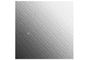
- 4 is an AFM photograph showing the structure of the upper surface of a second conductivity type cladding layer of a nitride semiconductor device according to an embodiment of the present disclosure.
- 4 is an SEM photograph showing the structure of the upper surface of a second conductivity type cladding layer of a nitride semiconductor device according to an embodiment of the present disclosure.
- 1 is an AFM photograph showing a structure of an upper surface of a second conductivity type cladding layer of a conventional nitride semiconductor device.
- 1 is a schematic plan view showing a configuration example of a nitride semiconductor device according to an embodiment of the present disclosure.
- 1 is a schematic cross-sectional view showing a configuration example of a nitride semiconductor device according to an embodiment of the present disclosure.
- 1 is a schematic cross-sectional view showing a configuration example of a nitride semiconductor device according to an embodiment of the present disclosure.
- 1 is a schematic cross-sectional view showing a configuration example of a nitride semiconductor device according to an embodiment of the present disclosure.
- the nitride semiconductor device according to this embodiment is, for example, a laser diode.
- the laser diode includes a nitride semiconductor substrate containing Al, and a semiconductor laminate disposed on the nitride semiconductor substrate.
- the semiconductor laminate includes a first-conductivity-type cladding layer containing a first-conductivity-type nitride semiconductor, a light-emitting layer disposed on the first-conductivity-type cladding layer and formed of a nitride semiconductor containing one or more quantum wells, and a second-conductivity-type cladding layer disposed on the light-emitting layer and formed of a second-conductivity-type nitride semiconductor containing Al.
- the surface of the second-conductivity-type cladding layer has a spiral-shaped step-terrace structure having terraces and steps other than linear in plan view.
- the nitride semiconductor substrate (hereinafter, sometimes referred to as substrate) includes a nitride semiconductor containing Al.
- the nitride semiconductor containing Al is, for example, AlN. That is, the substrate is preferably an AlN single crystal substrate.
- the nitride semiconductor containing Al is not limited to AlN, and may be, for example, AlGaN.
- the substrate is a nitride semiconductor single crystal substrate such as AlN or AlGaN
- the difference in lattice constant with the nitride semiconductor layer formed on the substrate becomes small, and the nitride semiconductor layer is grown in a lattice-matched system, thereby reducing threading dislocations.
- the threading dislocation density of the substrate is preferably 5 ⁇ 10 4 cm ⁇ 2 or less.
- the threading dislocation density is more preferably 1 ⁇ 10 3 cm ⁇ 2 or more and 1 ⁇ 10 4 cm ⁇ 2 or less.
- the substrate may be formed on a substrate of a different type so long as it contains a nitride semiconductor containing Al.
- AlN may be grown on a sapphire (Al 2 O 3 ) substrate.
- the layer mainly contains a nitride semiconductor means that the layer mainly contains a nitride semiconductor, but this expression also includes cases where other elements are included. Specifically, this expression also includes cases where the composition of this layer is slightly changed by adding a small amount of an element other than a nitride semiconductor (for example, a few percent or less of elements such as Ga (when Ga is not the main element), In, As, P, or Sb). In expressions regarding the composition of other layers, the wording "including” has a similar meaning. Furthermore, the small amount of elements contained is not limited to the above.
- the substrate preferably has a layer thickness of 100 ⁇ m or more and 600 ⁇ m or less.
- the surface orientation may be c-plane (0001), a-plane (11-20), m-plane (10-10), etc., with a c-plane (0001) substrate being more preferable.
- it may be formed on a surface inclined at some angle (for example, -4° to 4°, preferably -0.4° to 0.4°) from the normal direction of the c-plane (0001), but is not limited to this.
- a buffer layer may be formed on the substrate, i.e., between the substrate and the first conductive type cladding layer.
- the buffer layer is preferably formed on the entire surface of the substrate.
- a nitride semiconductor layer having small lattice constant differences and thermal expansion coefficient differences and few defects is formed on the buffer layer.
- the buffer layer is preferably a nitride semiconductor layer containing Al, and is formed of, for example, a nitride semiconductor such as AlN, AlGaN, etc.
- the buffer layer may also contain impurities such as C, Si, Fe, Mg, etc.
- the buffer layer has a thickness of, for example, several micrometers. Specifically, the thickness of the buffer layer is preferably greater than 10 nm and less than 10 ⁇ m. If the buffer layer is greater than 10 nm, the crystallinity of the nitride semiconductor such as AlN is increased. Also, if the buffer layer is less than 10 ⁇ m thick, cracks are less likely to occur in the buffer layer formed by crystal growth over the entire surface of the wafer.
- the first-conductivity-type cladding layer is formed on a substrate.
- the word “on” in the expression “the first-conductivity-type cladding layer is formed on a substrate” means that the first-conductivity-type cladding layer is formed on one side of the substrate.
- the above expression also includes a case where another layer exists between the substrate and the first-conductivity-type cladding layer.
- the word “on” has the same meaning in other relationships between layers.
- the expression “the second-conductivity-type cladding layer is formed on the first-conductivity-type waveguide layer described later with an electron blocking layer interposed therebetween is also included in the expression.
- the terms “first conductivity type” and “second conductivity type” refer to semiconductors exhibiting different conductivity types, and for example, when one is n-type conductivity, the other is p-type conductivity.
- the first conductive cladding layer is a layer of a nitride semiconductor containing Al and Ga.
- the first conductive cladding layer is formed of, for example, Al a Ga (1-a) N (0 ⁇ a ⁇ 1). This makes it possible to enhance the crystallinity of the light emitting layer and improve the light emitting efficiency when a material corresponding to the band gap energy of the deep ultraviolet region is formed as the light emitting layer.
- the nitride semiconductor constituting the first conductive cladding layer is preferably a mixed crystal of AlN and GaN.
- the first conductive cladding layer is formed of Al a Ga (1-a) N (0.65 ⁇ a ⁇ 0.9).
- the first conductivity type cladding layer may be a graded layer in which the Al composition increases with increasing distance from the substrate for the purpose of controlling the longitudinal conductivity, etc.
- the above-mentioned limitation on the Al composition may be the Al composition obtained by averaging the Al composition at positions in the first conductivity type cladding layer in the thickness direction over the thickness of the first conductivity type cladding layer.
- the first conductivity type cladding layer is an n-type conductive semiconductor layer, it may contain impurities such as P, As, Sb, and other Group V elements other than N, C, H, F, O, Mg, Si, etc., but the types of impurity elements are not limited to these.
- the impurity contained in the first conductivity type cladding layer is preferably Si, and the impurity concentration is preferably 5 ⁇ 10 18 cm -3 or more and 5 ⁇ 10 19 cm -3 or more.
- the resistivity of the first conductivity type cladding layer is preferably 1 ⁇ 10 ⁇ 3 ⁇ cm or more and 5 ⁇ 10 ⁇ 3 ⁇ cm or less, which allows efficient carrier injection.
- the first conductivity type cladding layer preferably has a layer thickness of 250 nm or more and 800 nm or less, and more preferably has a layer thickness of 300 nm or more and 450 nm or less.
- the light emitting layer is a layer of a nitride semiconductor containing Al and Ga.
- the nitride semiconductor contained in the light emitting layer is preferably a mixed crystal of, for example, AlN or GaN, and is formed, for example, of Al b Ga (1-b) N (0 ⁇ b ⁇ 1).
- the light emitting layer may contain impurities such as Group V elements other than N, such as P, As, Sb, and C, H, F, O, Mg, and Si, but the types of impurity elements are not limited to these.
- the light-emitting layer may have either a multiple quantum well structure or a single quantum well structure.
- the number of quantum well structures is preferably between 1 and 5.
- ⁇ which indirectly represents the potential fluctuation of the nitride semiconductor layer, is preferably 130 meV or more and 350 meV or less.
- the nitride semiconductor layer represented by such ⁇ may be not only the light emitting layer but also a first conductivity type waveguide layer or a second conductivity type waveguide layer described later.
- ⁇ of the light emitting layer, the first conductivity type waveguide layer, or the second conductivity type waveguide layer is 130 meV or more and 350 meV or less, recombination of localized carriers occurs efficiently, and the light emission efficiency can be improved.
- the “potential fluctuation of the nitride semiconductor layer” is an index for specifying the distribution state of Ga in the surface direction of the nitride semiconductor layer
- “ ⁇ indirectly expressing the potential fluctuation” is an index showing the deviation from the uniformity of the alloy in the surface direction of the nitride semiconductor layer.
- the possible values of the half-width of the emission spectrum also differ depending on the Al composition of the nitride semiconductor. Therefore, the potential fluctuation of the nitride semiconductor layer is evaluated using ⁇ , which expresses the deviation from the half-width of the emission spectrum in a uniform state at each Al composition.
- the thickness of the region where the Al concentration profile changes gradually at the interface between the well layer and the barrier layer in the light-emitting layer is preferably 0.3 nm or more and 0.6 nm or less. This improves carrier confinement and increases the emission intensity.
- the laser diode of this embodiment may include waveguide layers formed above and below the light emitting layer so as to sandwich the light emitting layer and having the effect of confining light emitted from the light emitting layer within the light emitting layer.
- the waveguide layers are preferably composed of two layers, a first conductive type waveguide layer disposed between the first conductive type cladding layer and the light emitting layer, and a second conductive type waveguide layer disposed between the second conductive type cladding layer and the light emitting layer.
- the laser diode of this embodiment may include, for example, a first-conductivity-type waveguide layer disposed between the first-conductivity-type cladding layer and the light-emitting layer to confine light in the light-emitting layer, and a second-conductivity-type waveguide layer disposed between the second-conductivity-type cladding layer and the light-emitting layer to confine light in the light-emitting layer.
- the waveguide layer is preferably a nitride semiconductor containing Al and Ga having a band gap with a higher energy than the light emitting layer.
- the waveguide layer preferably has an Al composition and a film thickness that increase the electric field intensity distribution of light present in the device and the overlap of the light emitting layer.
- the light emitting layer is Al b Ga (1-b) N (0 ⁇ b ⁇ 1) and the waveguide layer is Al c Ga (1-c) N (0 ⁇ c ⁇ 1), it is more preferable that b ⁇ c and c ⁇ b+0.05.
- the total thickness of the waveguide layers is preferably 70 nm or more and 150 nm or less.
- the waveguide layer may contain impurities such as P, As, Sb, and other Group V elements other than N, C, H, F, O, Mg, Si, etc., but the types of impurity elements are not limited to these.
- the impurity contained in the first conductivity type waveguide layer is preferably Si, and the impurity concentration is preferably 5 ⁇ 10 18 cm -3 or more and 5 ⁇ 10 19 cm -3 or less.
- the Al composition of each of the first conductivity type waveguide layer and the second conductivity type waveguide layer is preferably uniform in the film thickness direction, but is not limited to this.
- the Al composition of the second conductivity type waveguide layer may be higher than the Al composition of the first conductivity type waveguide layer.
- the film thickness of the second conductivity type waveguide layer may be thicker than the film thickness of the first waveguide.
- the second conductivity type cladding layer is formed on the light emitting layer and is a nitride semiconductor layer containing Al and Ga having second conductivity type conductivity.
- the second conductivity type cladding layer is formed of, for example, Al d Ga (1-d) N (0.1 ⁇ d ⁇ 1).
- the second conductivity type cladding layer is formed on the second conductivity type waveguide layer. This allows the second conductivity type cladding layer to easily lattice match with the light emitting layer or the waveguide layer, and makes it possible to suppress threading dislocation density.
- the second conductivity type cladding layer is not particularly limited as long as it has sufficient conductivity to inject carriers (electrons or holes) into the light-emitting layer and can increase the overlap between the electric field strength distribution of the optical mode present in the device and the light-emitting layer (i.e., increase the light confinement).
- the second conductivity type cladding layer may be, for example, p-type AlGaN doped with Mg.
- the second conductivity type cladding layer may also contain impurities such as P, As, Sb, and other group V elements other than N, C, H, F, O, Mg, and Si, but the types of impurity elements are not limited to these.
- the second conductivity type cladding layer is a compositionally graded layer formed of Al d Ga (1-d) N (0.1 ⁇ d ⁇ 1) in which the Al composition d decreases with increasing distance from the substrate as a whole, while in a portion of the second conductivity type cladding layer, the Al composition d increases with increasing distance from the substrate.
- the second conductive type cladding layer preferably has a composition gradient in which the Al composition d decreases in the range of 1 to 0.7 with increasing distance from the nitride semiconductor substrate side.
- the profile (gradient) of the Al composition d in the second conductive type cladding layer may decrease continuously or may decrease intermittently.
- the second conductive type cladding layer includes a part in which the Al composition d is the same (constant in the film thickness direction).
- the second conductive type cladding layer may include a part in which the Al composition d does not decrease (a part in which the Al composition d is constant or increases) in the direction away from the substrate.
- the thickness of the second conductive cladding layer is preferably 500 nm or less from the viewpoint of lattice matching. Moreover, from the viewpoint of optical confinement, it is more preferable that the thickness is 250 nm or more and 500 nm or less.
- the second-conductivity-type cladding layer has a composition gradient such that the Al composition d decreases with increasing distance from the substrate.
- a portion of the second-conductivity-type cladding layer is doped with impurities such as carbon or oxygen.
- the impurities are also doped into an interface gradient portion on the second-conductivity-type waveguide layer where the Al composition increases, for example, so that the concentration profile increases discontinuously at the start point of the composition gradient layer (the interface on the second-conductivity-type waveguide layer side).
- the second conductivity type cladding layer is often formed of a nitride semiconductor that is doped with almost no impurities for the purpose of suppressing the diffusion of impurities and improving injection efficiency, etc.
- impurities for the purpose of suppressing the diffusion of impurities and improving injection efficiency, etc.
- the second conductive type cladding layer has at least one region where the concentration profile of carbon or oxygen contained in the second conductive type cladding layer changes discontinuously as it moves away from the substrate.
- the impurity concentration profile has a region that is convex in the direction of increasing concentration.
- the concentration profile of carbon or oxygen in the second conductive type cladding layer slopes at a steep slope, improving the effect of improving the injection efficiency of carriers into the light-emitting layer, and the second conductive type cladding layer can achieve both the effect of suppressing deterioration of the second conductive type cladding layer and the effect of improving the injection efficiency of carriers into the light-emitting layer.
- the impurity concentration profile has a region that is convex in the direction in which the concentration increases, this is disadvantageous in terms of the efficiency of carrier injection into the light-emitting layer; however, depending on the thickness of the second cladding layer, providing a region in which the carbon or oxygen concentration profile has a steep slope can be advantageous overall in terms of the efficiency of carrier injection into the light-emitting layer.
- a region in which the concentration profile discontinuously decreases with increasing distance from the substrate (nitride semiconductor substrate) at at least one point refers to a region in which the impurity concentration in a certain region (the impurity concentration measured at a measurement point in that region) differs by a factor of two or more from the surrounding impurity concentration (the impurity concentration measured at a measurement point in an adjacent region).
- the impurity concentration profile changes abruptly.
- the second conductivity type cladding layer has a region P where the impurity concentration profile decreases discontinuously.
- the region P where the concentration profile decreases discontinuously is preferably present in a region from 1 nm to 110 nm from the substrate side of the second conductivity type cladding layer, and more preferably in a region from 5 nm to 110 nm. This makes it possible to suppress deterioration of the second conductivity type cladding layer without impeding the improvement of the efficiency of carrier injection into the light-emitting layer.
- the region of the second conductive type cladding layer closer to the substrate than the region P where the impurity concentration profile discontinuously decreases is preferably made of Al e Ga (1-e) N (0.8 ⁇ e ⁇ 1.0), which makes it possible to suppress deterioration of the second conductive type cladding layer without impeding the improvement of the efficiency of carrier injection into the light emitting layer.
- the carbon concentration in a region closer to the substrate than the region P where the impurity concentration profile decreases discontinuously is preferably 1 ⁇ 10 17 cm ⁇ 3 or more and 1 ⁇ 10 18 cm ⁇ 3 or less.
- the oxygen concentration in a region closer to the substrate than the region P where the impurity concentration profile decreases discontinuously is preferably 1 ⁇ 10 17 cm ⁇ 3 or more and 1 ⁇ 10 18 cm ⁇ 3 or less.
- the second conductivity type cladding layer has the composition discontinuous region Q, and the laser diode can achieve both the effect of suppressing deterioration of the second conductivity type cladding layer and the effect of improving the efficiency of carrier injection into the light emitting layer.
- Composition discontinuous region Q is preferably present in a region of 1 nm or more and 110 nm or less from the nitride semiconductor substrate side of the second conductivity type cladding layer, and more preferably in a region of 5 nm or more and 110 nm or less. That is, the start point of composition discontinuous region Q preferably coincides with the start point of region P.
- the composition discontinuous region Q has a composition gradient in which the Al composition d increases from 0.002 to 0.05 with increasing distance from the substrate.
- a layer that is effective in suppressing deterioration of the second conductive type cladding layer and a layer that is effective in improving the injection efficiency of carriers into the light emitting layer are formed. Therefore, it is possible to more effectively achieve both the effect of suppressing deterioration of the second conductive type cladding layer in the laser diode and the effect of improving the injection efficiency of carriers into the light emitting layer.
- the interface of the second conductivity type cladding layer on the substrate side preferably contains hydrogen at a concentration of 1 ⁇ 10 17 cm ⁇ 3 or more and 5 ⁇ 10 19 cm ⁇ 3 or less.
- At least a portion of the second conductivity type cladding layer preferably contains hydrogen at a higher concentration than other regions of the second conductivity type cladding layer.
- the second conductivity type cladding layer of the laser diode of this embodiment includes a region (the portion) partially containing a high concentration of hydrogen. This allows the laser diode to compensate for point defects and achieve both the effect of suppressing deterioration of the second conductivity type cladding layer and the effect of improving the efficiency of carrier injection into the light emitting layer.
- the region containing hydrogen at a higher concentration than other regions of the second conductive type cladding layer is preferably a region of 1 nm or more and 110 nm or less from the substrate side of the second conductive type cladding layer, and more preferably a region of 5 nm or more and 110 nm or less, which makes it possible to compensate for point defects and suppress deterioration of the second conductive type cladding layer without impeding the improvement of the efficiency of carrier injection into the light emitting layer.
- the half width of the hydrogen concentration profile in the region containing hydrogen at a higher concentration than other regions of the second conductivity type cladding layer is preferably 5 nm to 10 nm, which makes it possible to effectively compensate for point defects and improve the efficiency of carrier injection into the light emitting layer.
- the interface of the second conductivity type cladding layer on the substrate side may contain silicon at a concentration of 1 ⁇ 10 17 cm -3 or more and 5 ⁇ 10 19 cm -3 or less. At least a portion of the second conductivity type cladding layer may contain silicon at a higher concentration than other regions of the second conductivity type cladding layer.
- the region containing silicon at a higher concentration than other regions of the second conductivity type cladding layer is preferably a region 1 nm or more and 110 nm or less from the substrate side of the second conductivity type cladding layer, and more preferably a region 5 nm or more and 110 nm or less.
- the surface of the second conductive cladding layer as described above has a spiral step-terrace structure having terraces and steps other than linear in plan view, as shown in FIG. 2A.
- An example of the spiral step-terrace structure is a hexagonal shape with one side of the outline gradually becoming shorter.
- Other examples of the spiral step-terrace structure are a circular shape with a gradually shortened radius, or a mixed shape of a hexagon and a straight line with a gradually shortened side length.
- FIG. 3 shows a step-terrace structure having linear terraces and steps in plan view. This makes it possible to better achieve both the effect of suppressing deterioration of the second conductive cladding layer in the laser diode and the effect of improving the injection efficiency of carriers into the light emitting layer.
- FIG. 2A is an atomic force microscope (AFM) photograph showing the spiral step-terrace structure
- FIG. 2B is a scanning electron microscope (SEM) photograph showing the circular step-terrace structure.
- the spiral step-terrace structure provides a higher effect of improving the luminous efficiency of the second conductive type cladding layer. This is believed to be because Ga is segregated during the growth of the film with the spiral step-terrace structure, improving the current injection efficiency.
- the height of the spiral step-terrace structure is preferably 0.2 nm or more and 0.4 nm or less.
- the distribution density of the spiral step-terrace structure is preferably 1 ⁇ 10 7 cm ⁇ 2 or more and 5 ⁇ 10 8 cm ⁇ 2 or less. This makes it possible to obtain a further improved effect of suppressing deterioration of the second conductivity type cladding layer and to improve the current injection efficiency.
- the spiral step-terrace structure when a nitride semiconductor layer having a spiral step-terrace structure is formed and then a nitride semiconductor layer is formed by a conventional method to form a second conductive cladding layer, the spiral step-terrace structure also appears on the surface of the second conductive cladding layer. Therefore, by observing the surface shape of the second conductive cladding layer, the spiral step-terrace structure on the surface of the second conductive cladding layer can be confirmed. In addition, when a second conductive contact layer, which will be described later, is formed on the second conductive cladding layer, the spiral step-terrace structure does not appear on the surface of the second conductive contact layer.
- the laser diode according to this embodiment may have an interface slope portion on the light emitting layer (second conductivity type waveguide) that contains Al g Ga (1-g) N (0.1 ⁇ g ⁇ 1) and the Al composition g increases with increasing distance from the nitride semiconductor substrate.
- the interface slope portion As in this embodiment, the electric field is relaxed, and the degradation suppression effect is improved.
- the thickness of the inclined interface portion is preferably 2 nm to 5 nm, more preferably 2 nm to 3 nm, in which case the degradation suppression effect is further improved.
- the semiconductor laminate of the laser diode of this embodiment may further include a second-conductivity-type contact layer disposed on the second-conductivity-type cladding layer.
- the nitride semiconductor constituting the second-conductivity-type contact layer is preferably formed of, for example, GaN, AlN, or InN, or a mixed crystal containing these, and more preferably is a nitride semiconductor containing GaN.
- the second conductive type contact layer may contain impurities such as P, As, Sb, and other V group elements other than N, C, H, F, O, Mg, Si, and Be.
- the impurity contained in the second conductive type contact layer is preferably Mg.
- the concentration of Mg is preferably 8 ⁇ 10 19 cm -3 or more and 5 ⁇ 10 21 cm -3 or less, and more preferably 5 ⁇ 10 20 cm -3 or more and 5 ⁇ 10 21 cm -3 or less.
- the thickness of the second conductive contact layer is preferably 1 nm or more and 20 nm or less. The thinner the second conductive contact layer is, the more efficient the carrier injection into the light-emitting layer is, and the thicker the layer is, the more efficient the carrier injection is.
- the semiconductor laminate of the laser diode of this embodiment may further include an electron blocking layer above the light emitting layer, the electron blocking layer having a band gap larger than that of the light emitting layer.
- the electron blocking layer may be provided, for example, on the light emitting layer, or may be provided inside the second conductive type waveguide layer, between the second conductive type waveguide layer and the light emitting layer, or between the second conductive type waveguide layer and the second conductive type cladding layer.
- the thickness of the electron blocking layer is preferably 30 nm or less, and more preferably 20 nm or less, so that carriers (holes) can easily quantum-transport through the electron blocking layer.
- the laser diode can emit light or oscillate by injecting a current through a second electrode disposed on the second conductive type cladding layer and a first electrode disposed on the first conductive type cladding layer, where the first electrode is formed so as to be in electrical contact with the first conductive type cladding layer, and the second electrode is formed so as to be in electrical contact with the second conductive type cladding layer.
- the first electrode can be disposed, for example, on the back side of the substrate.
- the first electrode is also disposed on the first conductivity type cladding layer that is exposed by removing the layers above the first conductivity type cladding layer of the semiconductor laminate by, for example, chemical etching or dry etching.
- the first electrode is disposed on a region of the first conductivity type cladding layer that does not form a mesa structure.
- the first electrode is formed of a metal such as Al, Ti, Zr, Hf, V, Nb, Ta, Cr, Mo, W, Co, Rh, Ir, Ni, Pd, Pt, Cu, Ag, Au, Zr, or a mixed crystal thereof, or a conductive oxide such as ITO or Ga2O3 .
- the first electrode is formed of a metal such as Ni, Au, Pt, Ag, Rh, Pd, Pt, Cu, Al, Ti, Zr, Hf, V, Nb, Ta, Cr, Mo, W, Co, Ir, Zr, or a mixed crystal thereof, or a conductive oxide such as ITO or Ga2O3 .
- the second electrode is formed of a metal such as Al, Ti, Zr, Hf, V, Nb, Ta, Cr, Mo, W, Co, Rh, Ir, Ni, Pd, Pt, Cu, Ag, Au, Zr, or a mixed crystal thereof, or a conductive oxide such as ITO or Ga2O3 .
- the second electrode is formed of a metal such as Ni, Au, Pt, Ag, Rh, Pd, Pt, Cu, Al, Ti, Zr, Hf, V, Nb, Ta, Cr, Mo, W, Co, Ir, Zr, or a mixed crystal thereof, or a conductive oxide such as ITO or Ga2O3 .
- the arrangement area and shape of the first electrode and the second electrode are not limited as long as electrical contact is obtained with the first conductivity type clad layer and the second conductivity type clad layer (or the second conductivity type contact layer if a second conductivity type contact layer is provided).
- the laser diode which is the nitride semiconductor device of this embodiment, can be manufactured by singulating a nitride semiconductor stack manufactured through a process of forming each nitride semiconductor layer on a substrate.
- a method for manufacturing a nitride semiconductor stack and a method for manufacturing a laser diode as an example of a method for manufacturing a nitride semiconductor device will be described.
- the substrate is formed by a general substrate growth method such as a vapor phase growth method, such as a sublimation method or a hydride vapor phase epitaxy (HVPE) method, or a liquid phase growth method.
- a general substrate growth method such as a vapor phase growth method, such as a sublimation method or a hydride vapor phase epitaxy (HVPE) method, or a liquid phase growth method.
- Each layer of the semiconductor laminate layer formed on the substrate can be formed by, for example, a molecular beam epitaxy (MBE) method, a hydride vapor phase epitaxy (HVPE) method, or a metal organic chemical vapor deposition (MOCVD) method.
- MBE molecular beam epitaxy
- HVPE hydride vapor phase epitaxy
- MOCVD metal organic chemical vapor deposition
- the nitride semiconductor layer can be formed using, for example, an Al source containing trimethylaluminum (TMAl), a Ga source containing trimethylgallium (TMGa) or triethylgallium (TEGa), or the like, or a N source containing ammonia (NH 3 ).
- a semiconductor laminate layer is formed on the substrate. At this time, an organometallic gas is flowed into the semiconductor laminate layer formation space. First, a first conductivity type cladding layer containing a first conductivity type nitride semiconductor is formed on the substrate.
- a first conductivity type waveguide layer made of a nitride semiconductor such as AlGaN is formed on the first conductivity type cladding layer, and then a light emitting layer is formed from a nitride semiconductor (such as AlGaN) that includes one or more quantum wells.
- a second conductivity type waveguide layer made of a nitride semiconductor such as AlGaN is formed on the light emitting layer.
- the first conductivity type waveguide layer, the light emitting layer and the second conductivity type waveguide layer are preferably formed under conditions that satisfy ⁇ 2Tw+2050 ⁇ Vw ⁇ 2Tw+2350 (850° C. ⁇ Tw ⁇ 970° C.), where Tw is the wafer temperature and Vw is the reactor pressure.
- Tw is the wafer temperature
- Vw is the reactor pressure.
- a second conductivity type cladding layer is formed on the second conductivity type waveguide layer.
- the flow of the metal-organic gas is temporarily stopped to interrupt the growth of the nitride semiconductor layer, and the film formation conditions are changed.
- the flow of the metal organic gas is temporarily stopped again to interrupt the growth of the nitride semiconductor layer and the film formation conditions are changed.
- the wafer temperature is changed to 1030° C. to 1100° C.
- the reactor pressure is changed to 15 mbar to 350 mbar, and the flow of the metalorganic gas is resumed to form the remaining part of the second conductivity type cladding layer.
- the first conductivity type cladding layer, the first conductivity type waveguide layer, the light emitting layer, and the second conductivity type waveguide layer in the above manner, it is possible to increase the recombination rate of carriers and reduce point defects in each layer, thereby suppressing degradation and improving the light emitting efficiency. Furthermore, by setting the wafer temperature when forming a portion of the second conductivity type cladding layer lower than the wafer temperature when forming the remaining portion of the second conductivity type cladding layer, it is possible to form at least one region in which the carbon or oxygen concentration profile in the portion of the second conductivity type cladding layer and the remaining portion of the second conductivity type cladding layer discontinuously decreases with increasing distance from the substrate.
- the portion of the second conductivity type cladding layer can be formed to contain more carbon or oxygen than the remaining portion of the second conductivity type cladding layer. This makes it possible to achieve both suppression of deterioration and improvement of injection efficiency in the second conductivity type cladding layer. Furthermore, by setting the reactor pressure when forming a portion of the second conductivity type cladding layer lower than the reactor pressure when forming the remaining portion of the second conductivity type cladding layer, the portion of the second conductivity type cladding layer can be formed to contain more carbon or oxygen as an impurity compared to the remaining portion of the second conductivity type cladding layer.
- hydrogen and silicon are localized at the interface of the second-conductivity-type cladding layer on the substrate side.
- hydrogen gas (H 2 ) is used as the carrier gas
- hydrogen (H) is likely to be localized in the uppermost layer of the nitride semiconductor layer where the growth is interrupted (for example, the interface between the second-conductivity-type waveguide layer and the second-conductivity-type cladding layer and a part of the second-conductivity-type cladding layer).
- This allows the laser diode to further improve the effect of suppressing deterioration of the second-conductivity-type cladding layer and the effect of improving the efficiency of carrier injection into the light-emitting layer.
- the wafer temperature when forming a portion of the second conductivity type cladding layer is set lower than the wafer temperature when forming the remaining portion of the second conductivity type cladding layer, thereby forming at least one region in which the carbon or oxygen concentration profile in the portion of the second conductivity type cladding layer and the remaining portion of the second conductivity type cladding layer discontinuously decreases with increasing distance from the substrate, but the manufacturing method is not limited to this.
- the flow rate of the organometallic gas may be intentionally changed during the formation of the second conductivity type cladding layer to form a region in which the carbon or oxygen concentration profile discontinuously decreases with increasing distance from the substrate.
- an intermediate layer may be formed between the second conductive cladding layer and the second conductive waveguide layer using a nitride semiconductor such as AlGaN, a second conductive contact layer may be provided on the second conductive cladding layer using a nitride semiconductor including GaN, or an electron blocking layer may be formed above the light emitting layer.
- a nitride semiconductor such as AlGaN
- a second conductive contact layer may be provided on the second conductive cladding layer using a nitride semiconductor including GaN
- an electron blocking layer may be formed above the light emitting layer.
- Laser diodes are manufactured through a process of forming a semiconductor laminate by removing unnecessary portions of each layer of a semiconductor laminate formed on a substrate by etching (mesa structure forming process).
- the unnecessary portions of each layer of the semiconductor laminate can be removed by, for example, inductively coupled plasma (ICP) etching.
- ICP inductively coupled plasma
- unnecessary portions of each layer of the conductor laminate layer are removed by etching, thereby exposing a portion of the first conductivity type cladding layer.
- the laser diode may be manufactured through a process of forming electrodes.
- the electrodes such as the first electrode and the second electrode, may be formed by various methods of evaporating metal by an electron beam deposition (EB) method, such as resistance heating deposition, electron gun deposition, or sputtering, but are not limited to these methods.
- EB electron beam deposition
- Each electrode may be formed as a single layer or may be formed by laminating multiple layers.
- each electrode may be subjected to a heat treatment in an oxygen, nitrogen or air atmosphere after the metal layer is formed.
- the substrate on which the layers have been formed through the above-mentioned steps is divided into individual pieces by dicing to manufacture nitride semiconductor devices (laser diodes).
- a first electrode is formed on the surface of the first conductive cladding layer.
- the second electrode is formed on the top layer (e.g., the second conductive cladding layer) of a mesa structure that is a part of the semiconductor laminate.
- the formed electrode is alloyed by heating with a rapid thermal annealing (RTA) device, which is a heating process using an infrared lamp, or by laser annealing, which is a heating process using a laser pulse, to obtain contact with the semiconductor laminate.
- RTA rapid thermal annealing
- the method of alloying is not particularly limited as long as sufficient contact with the semiconductor laminate can be obtained.
- the carrier injection efficiency can be improved, and the emission intensity can be increased.
- the thickness of each layer constituting the laser diode can be measured by cutting out a predetermined cross section perpendicular to the substrate, observing this cross section with a transmission electron microscope (TEM), and using the length measurement function of the TEM.
- TEM transmission electron microscope
- a measurement method first, a cross section perpendicular to the main surface of the substrate of the laser diode is observed using a TEM.
- the observation width is set to a range of 2 ⁇ m or more in a direction parallel to the main surface of the substrate in a TEM image showing a cross section perpendicular to the main surface of the substrate of the laser diode.
- the thickness to this interface is observed in a continuous observation region with a width of 200 nm.
- the average value of the thickness of each layer included in this 200 nm wide observation region can be calculated from five points arbitrarily extracted from the above-mentioned observation width of 2 ⁇ m or more to obtain the layer thickness of each layer.
- the concentration of dopants and impurities contained in each layer constituting the laser diode can be measured by secondary ion mass spectrometry (SIMS).
- SIMS secondary ion mass spectrometry
- the concentration of dopants and impurities contained in each layer can be measured by SIMS after processing into a device, the measurement can be performed in a state where the electrodes are removed by chemical etching or physical polishing.
- the concentration of dopants and impurities contained in each layer can also be measured by sputtering from the substrate side where no electrodes are formed.
- the SIMS measurement is performed under the measurement conditions provided by Evans Analytical Group (EAG), Inc.
- a cesium (Cs) ion beam having an energy of 14.5 keV is used for sputtering the sample during the measurement.
- a method for measuring the atomic concentration in each layer constituting a laser diode includes reciprocal space mapping (RSM) using X-ray diffraction (XRD).
- RSM reciprocal space mapping
- XRD X-ray diffraction
- the lattice relaxation rate and Al composition relative to the underlayer can be obtained by analyzing reciprocal space mapping data in the vicinity of a diffraction peak obtained with an asymmetric plane as a diffraction plane.
- the diffraction plane include the (10-15) plane and the (20-24) plane.
- layers and regions that do not provide sufficient reflection intensity by XRD can be measured using X-ray photoelectron spectroscopy (XPS), energy dispersive X-ray spectroscopy (EDX), and electron energy-loss spectroscopy (EELS).
- XPS X-ray photoelectron spectroscopy
- EDX energy dispersive X-ray spectroscopy
- EELS electron energy-loss spectroscopy
- the composition of a sample is analyzed by measuring the energy lost when an electron beam passes through the sample.
- the energy loss spectrum of the intensity of the transmitted electron beam is measured and analyzed for a thin-sectioned sample used in TEM observations.
- the position of the peak that appears at an energy loss of around 20 eV changes depending on the composition of each layer, and the composition can be determined from the peak position.
- the Al composition of each layer is obtained by calculating the average value of the Al composition in an observation width of 200 nm from five points randomly selected from an observation area of 2 ⁇ m or more.
- the EDX measures and analyzes the characteristic X-rays generated by the electron beam in the thin-sectioned sample used in the above-mentioned TEM observation.
- the Al composition of each layer is obtained by calculating the average value of the Al composition in an observation width of 200 nm from five points randomly selected from an observation area of 2 ⁇ m or more.
- XPS depth direction evaluation is possible by performing XPS measurement while performing sputter etching using an ion beam.
- Ar+ is generally used for the ion beam
- other ion species such as Ar cluster ions can be used as long as they can be irradiated with the etching ion gun mounted on the XPS device.
- the XPS peak intensities of Al, Ga, and N are measured and analyzed to obtain the depth direction distribution of the Al composition of each layer.
- the laser diode can be polished at an angle so that a cross section perpendicular to the main surface of the substrate is enlarged and exposed, and the exposed cross section can be measured by XPS.
- the composition of each layer can be measured not only by XPS but also by Auger Electron Spectroscopy (AES). In this case, the composition can be measured by performing Auger Electron Spectroscopy on a cross section exposed by sputter etching or angled polishing. The composition of each layer can also be measured by SEM-EDX measurement of a cross section exposed by angled polishing.
- AES Auger Electron Spectroscopy
- Methods for measuring the surface shape of the second conductivity type cladding layer include a scanning electron microscope (SEM) and an atomic force microscope (AFM). Specifically, the surface of the second conductive type cladding layer is observed using a scanning electron microscope SU9000 manufactured by Hitachi High-Tech Corporation at an accelerating voltage of 30 kV. At this time, the surface shape of the second conductive type cladding layer can be clearly observed by setting the magnification to 10K to 50K. Under these conditions, the number of spiral step-terrace structures contained within the observation range is counted, and the value obtained by dividing the number by the area is taken as the density of the spiral step-terrace structures.
- SEM scanning electron microscope
- AFM atomic force microscope
- the step height of the spiral step-terrace structure on the surface of the second conductive type cladding layer can be measured by AFM. Specifically, the observation is performed using a scanning probe microscope manufactured by Hitachi High-Tech Corporation. When observing with the scanning probe microscope, the AFM mode is used to observe an area of 2 ⁇ m square. The step height can be obtained from the obtained AFM measurement.
- the laser diode according to the present disclosure can be applied to devices in, for example, the medical and life science fields, the environmental field, the industrial and manufacturing fields, the household appliances field, the agricultural field, and other fields.
- the laser diode can be applied to a drug or chemical synthesis/decomposition device, a liquid/gas/solid (container, food, medical equipment, etc.) sterilization device, a semiconductor cleaning device, etc., a surface modification device for film, glass, metal, etc., an exposure device for manufacturing semiconductors, FPD (Flat Panel Display), PCB (Printed Wiring Board), and other electronic products, a printing/coating device, an adhesive/sealing device, a transfer/molding device for film, pattern, mockup, etc., and a measurement/inspection device for banknotes, wounds, blood, chemical substances, etc.
- a drug or chemical synthesis/decomposition device e.g., a liquid/gas/solid (container, food, medical equipment, etc.) sterilization device, a semiconductor cleaning device, etc., a surface modification device for film, glass, metal, etc., an exposure device for manufacturing semiconductors, FPD (Flat Panel Display), PCB (Printed Wiring Board), and
- liquid sterilization equipment examples include, but are not limited to, automatic ice makers, ice trays and ice storage containers in refrigerators, water tanks for ice makers, freezers, ice makers, humidifiers, dehumidifiers, cold water tanks, hot water tanks and flow piping for water servers, freestanding water purifiers, portable water purifiers, water supply units, hot water heaters, wastewater treatment equipment, garbage disposers, toilet drain traps, washing machines, dialysis water sterilization modules, peritoneal dialysis connector sterilizers, disaster water storage systems, etc.
- gas sterilization devices include, but are not limited to, air purifiers, air conditioners, ceiling fans, floor or bedding vacuum cleaners, futon dryers, shoe dryers, washing machines, clothes dryers, indoor germicidal lamps, storage ventilation systems, shoe boxes, chests of drawers, etc.
- solid sterilization equipment include, but are not limited to, vacuum packing machines, belt conveyors, hand tool sterilization equipment for medical/dental use, barber shops/beauty salons, toothbrushes, toothbrush holders, chopstick cases, cosmetic pouches, drain covers, toilet spot cleaners, toilet lids, etc.
- the nitride semiconductor device according to this embodiment is, for example, a light emitting device.
- a case where the nitride semiconductor device is a light emitting device will be described.
- the light-emitting device includes a nitride semiconductor substrate containing Al, and a semiconductor laminate portion disposed on the nitride semiconductor substrate.
- the semiconductor laminate portion includes a first-conductivity-type cladding layer containing a first-conductivity-type nitride semiconductor, a light-emitting layer disposed on the first-conductivity-type cladding layer and formed of a nitride semiconductor containing one or more quantum wells, and a second-conductivity-type cladding layer disposed on the light-emitting layer and formed of a second-conductivity-type nitride semiconductor containing Al.
- the surface of the second-conductivity-type cladding layer has a spiral-shaped step-terrace structure having terraces and steps other than linear in plan view.
- the light emitting device of this embodiment differs from the laser diode of the first embodiment in that it does not include a first conductive type waveguide layer and a second conductive type waveguide layer.
- the second conductive type cladding layer may be used as a barrier layer.
- the light emitting device of this embodiment has a different configuration from the first conductive cladding layer of the laser diode of the first embodiment, so the first conductive cladding layer and the second conductive cladding layer of the light emitting device will be described in detail below. Note that the layers other than the first conductive type cladding layer, that is, the nitride semiconductor substrate, the buffer layer, and the light emitting layer, are similar to the layers described in the first embodiment, and therefore description thereof will be omitted.
- the first conductive type cladding layer is a nitride semiconductor layer containing Al and Ga.
- the first conductive type cladding layer is formed of, for example, Al a Ga (1-a) N (0 ⁇ a ⁇ 1), and is preferably formed of, for example, Al a Ga (1-a) N (0.7 ⁇ a ⁇ 1).
- the first conductivity type cladding layer is preferably made of an n-type semiconductor.
- the thickness T0 of the first conductivity type cladding layer is not less than 3300 ⁇ a ⁇ 2100 nm and not more than 15700 ⁇ a ⁇ 10100 nm (a is the proportion of Al atoms when the total number of group III atoms in the nitride semiconductor constituting the first conductivity type cladding layer is taken as 1).
- the resistivity of the first conductivity type cladding layer is preferably not less than 1 ⁇ 10 ⁇ 3 ⁇ cm and not more than 5 ⁇ 10 ⁇ 3 ⁇ cm. The rest of the configuration is similar to that of the first conductivity type cladding layer described in the first embodiment.
- ⁇ Second Conductive Type Cladding Layer> In the light-emitting device, instead of a second-conductivity-type cladding layer with a graded Al composition, an electron block layer with a constant Al composition is provided on the light-emitting layer, and a second-conductivity-type contact layer with a graded Al composition is provided on the electron block layer.
- the electron block layer and the second-conductivity-type contact layer with a graded Al composition together function as a cladding layer.
- the electron block layer and the second conductive type contact layer are regarded as a second conductive type cladding layer, the inflow of the organometallic gas is temporarily stopped before the growth of the electron block layer to interrupt the growth of the nitride semiconductor layer, and only a part of the electron block layer is grown at a low temperature.
- a light emitting device is obtained in which the concentration profile of carbon or oxygen decreases discontinuously, hydrogen is localized at the interface of the electron block layer on the light emitting layer side, and more impurities are contained in the electron block layer than in the past.
- the metalorganic gas after the growth of the electron blocking layer and before the growth of the second conductivity type contact layer to interrupt the growth of the nitride semiconductor layer, it becomes possible to impart hydrogen at a higher concentration to a region of the second conductivity type cladding layer (the layer combining the electron blocking layer and the second conductivity type contact layer) that is away from the nitride semiconductor substrate side by the thickness of the electron blocking layer than to other regions.
- the thickness of the electron blocking layer is preferably 10 nm or more and 15 nm or less.
- the region in which the concentration profile of carbon or oxygen contained in the electron blocking layer decreases discontinuously is preferably present in a region of 10 nm or more and 15 nm or less from the substrate side of the electron blocking layer.
- the light-emitting element according to this embodiment does not include a first conductivity type waveguide layer and a second conductivity type waveguide layer. This makes it difficult to evaluate ⁇ , which indirectly represents potential fluctuations. This is because, when attempting to evaluate ⁇ , which indirectly represents potential fluctuations, the quantized light-emitting layer is excited and a correct result cannot be obtained.
- a nitride semiconductor layer under the same conditions as in the first embodiment, it is possible to form a nitride semiconductor layer having ⁇ , which indirectly represents a similar potential fluctuation.
- Nitride semiconductor devices of the present embodiment will now be described in more detail with reference to Figures 4 to 7.
- the detailed configurations of the layers in the following examples are as described above.
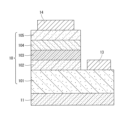
- FIG. 4 is a schematic cross-sectional view of a laser diode 1 as a first example.
- the laser diode 1 includes a substrate 11, a semiconductor laminate 10 disposed on the substrate, a first electrode 13, and a second electrode 14.
- the semiconductor laminate 10 includes a first conductivity type cladding layer 101 having an n-type conductivity, a first conductivity type waveguide layer 102, a light emitting layer 103, a second conductivity type waveguide layer 104, and a second conductivity type cladding layer 105 having a p-type conductivity.
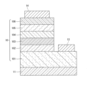
- FIG. 5 is a schematic cross-sectional view of a laser diode 2 as a second example.
- the laser diode 2 includes a substrate 11, a buffer layer 12, a semiconductor laminate 10 disposed on the substrate 11 (buffer layer 12), a first electrode 13, and a second electrode 14.
- the semiconductor laminate 10 includes a first conductivity type cladding layer 101 having an n-type conductivity, a first conductivity type waveguide layer 102, a light emitting layer 103, a second conductivity type waveguide layer 104, and a second conductivity type cladding layer 105 having a p-type conductivity. That is, the laser diode 2 differs from the laser diode 1 in that the laser diode 2 includes a buffer layer 12 .
- FIG. 6 is a schematic cross-sectional view of a laser diode 3 as a third example.
- the laser diode 3 includes a substrate 11, a buffer layer 12, a semiconductor laminate 10 disposed on the substrate, a first electrode 13, and a second electrode 14.
- the semiconductor laminate 10 includes a first conductivity type cladding layer 101 having an n-type conductivity type, a first conductivity type waveguide layer 102, a light emitting layer 103, a second conductivity type waveguide layer 104, a second conductivity type cladding layer 105 having a p-type conductivity type, and a contact layer 106.
- the laser diode 3 differs from the laser diode 1 in that the laser diode 3 includes a contact layer 106 .
- the laser diode of the present disclosure may have a configuration including the buffer layer 12 described in the second example and the contact layer 106 described in the third example.
- FIG. 7 is a schematic cross-sectional view of the light-emitting element 4, which is the first example.
- the light-emitting element 4 includes a substrate 11, a semiconductor laminate 10 disposed on the substrate, a first electrode 13, and a second electrode 14.
- the semiconductor laminate 10 includes a first conductive type cladding layer 101 having an n-type conductivity, a light-emitting layer 103, and a second conductive type cladding layer 105 having a p-type conductivity.
- an electron block layer and a second conductive type contact layer are provided to play the role of the second conductive type cladding layer 105.
- the light-emitting element 4 differs from the laser diode 1 in that it does not include the first-conductivity-type waveguide layer 102 and the second-conductivity-type waveguide layer 104.
- the light-emitting element 4 also differs from the laser diode 1 in that it is provided with an electron blocking layer and a second-conductivity-type contact layer that serves as the second-conductivity-type cladding layer 105.
- the light-emitting element of the present disclosure may have a configuration including the buffer layer 12 described in the second example.
- a nitride semiconductor device includes a nitride semiconductor substrate containing Al, and a semiconductor laminate disposed on the nitride semiconductor substrate.
- the semiconductor laminate includes a first-conductivity-type cladding layer containing a first-conductivity-type nitride semiconductor, a light-emitting layer disposed on the first-conductivity-type cladding layer and formed of a nitride semiconductor containing one or more quantum wells, and a second-conductivity-type cladding layer disposed on the light-emitting layer and formed of a second-conductivity-type nitride semiconductor containing Al.
- the surface of the second-conductivity-type cladding layer has a spiral-shaped step-terrace structure having terraces and steps other than linear in plan view. This makes it possible to more effectively suppress the deterioration of the second conductivity type cladding layer in the laser diode and to more effectively improve the efficiency of carrier injection into the light emitting layer.
- the height of the spiral step-terrace structure is preferably not less than 0.2 nm and not more than 0.4 nm. This further improves the current injection efficiency, and a higher effect of suppressing deterioration of the second conductivity type cladding layer can be obtained.
- the distribution density of the spiral step-terrace structure is preferably not less than 1 ⁇ 10 7 cm ⁇ 2 and not more than 5 ⁇ 10 8 cm ⁇ 2 . This further improves the current injection efficiency, and a higher effect of suppressing deterioration of the second conductivity type cladding layer can be obtained.
- a method for manufacturing a nitride semiconductor stack according to the present disclosure includes forming a first conductivity type cladding layer including a first conductivity type nitride semiconductor on a nitride semiconductor substrate including Al, forming a light emitting layer on the first conductivity type cladding layer using a nitride semiconductor including one or more quantum wells, forming a part of a second conductivity type cladding layer including a second conductivity type nitride semiconductor under conditions where the wafer temperature is from 900° C. to 1000° C. and the reactor pressure is from 15 mbar to 350 mbar, and forming a remaining part of the second conductivity type cladding layer under conditions where the wafer temperature is from 1030° C.
- the reactor pressure is from 15 mbar to 350 mbar, thereby forming a semiconductor stack on the nitride semiconductor substrate.
- the reactor pressure during the formation of a portion of the second conductivity type cladding layer is preferably 15 mbar or more and 100 mbar or less. This allows a portion of the second conductivity type cladding layer to be formed so as to contain more carbon or oxygen than the remaining portion of the second conductivity type cladding layer, thereby further improving the deterioration suppression effect and injection efficiency in the second conductivity type cladding layer.
- a nitride semiconductor stack it is preferable to flow an organometallic gas during the formation of the first conductivity type cladding layer, the light emitting layer, and the second conductivity type cladding layer, to temporarily stop the flow of the organometallic gas after the light emitting layer is formed and before forming a portion of the second conductivity type cladding layer, and to temporarily stop the flow of the organometallic gas after the portion of the second conductivity type cladding layer is formed and before forming the remaining portion of the second conductivity type cladding layer.
- the laser diode of the present disclosure will be described below with reference to examples and comparative examples, but the laser diode of the present disclosure is not limited to these examples.
- the substrate used was a (0001) AlN single crystal substrate having a thickness of 550 ⁇ m.
- an AlN layer which is a homoepitaxial layer, was formed on the substrate.
- the AlN layer was formed to a thickness of 500 nm in an environment at 1200° C.
- the ratio (V/III ratio) of the supply rate of the group III element source gas to the supply rate of the nitrogen source gas was set to 50.
- the growth rate of the AlN layer at this time was 0.5 ⁇ m/hr.
- Trimethylaluminum (TMAl) was used as the Al source.
- Ammonia (NH 3 ) was used as the N source.
- a first conductive cladding layer was formed on the substrate.
- the first conductive cladding layer was an n-type AlGaN layer (Al: 75%, i.e., an Al 0.75 Ga 0.25 N layer) using Si as a dopant impurity.
- the first conductive cladding layer was formed to a thickness of 400 nm under the conditions of a temperature of 1050° C., a reactor pressure of 50 mbar, and a V/III ratio of 4000.
- the growth rate of the first conductive cladding layer at this time was 0.4 ⁇ m/hr.
- Trimethylaluminum (TMAl) was used as the Al raw material.
- Triethylgallium (TEGa) was used as the Ga raw material.
- Ammonia (NH 3 ) was used as the N raw material.
- Monosilane (SiH 4 ) was used as the Si raw material.
- an n-type waveguide layer which is a first waveguide layer, was formed on the first conductive cladding layer.
- the n-type waveguide layer was an n-type AlGaN layer (Al: 63%, i.e., an Al0.63Ga0.37N layer) using Si as a dopant impurity.
- the n-type waveguide layer was formed to a thickness of 40 nm under the conditions of a temperature of 950°C, a reactor pressure of 300 mbar , and a V/III ratio of 4000.
- the growth rate of the n-type waveguide layer at this time was 0.35 ⁇ m/hr.
- Trimethylaluminum (TMAl) was used as the Al source
- triethylgallium (TEGa) was used as the Ga source
- ammonia (NH 3 ) was used as the N source.
- an emission layer was formed on the n-type waveguide layer.
- the emission layer was formed to have a multiple quantum well structure in which quantum well layers and barrier layers were stacked in two periods.
- the quantum well layer was an AlGaN layer (Al: 52%, i.e., an Al 0.52 Ga 0.48 N layer) having a thickness of 4.5 nm.
- the barrier layer was an AlGaN layer (Al: 63%, i.e., an Al 0.63 Ga 0.37 N layer) having a thickness of 6.0 nm.
- the light-emitting layer was formed at a temperature of 950° C., with a reactor pressure of 300 mbar and a V/III ratio of 4000.
- the growth rate of the quantum well layer was 0.18 ⁇ m/hr, and the growth rate of the barrier layer was 0.15 ⁇ m/hr.
- a p-type waveguide layer which is a second waveguide layer, was formed on the light emitting layer.
- the p-type waveguide layer was an AlGaN layer (Al: 63%, i.e., an Al 0.63 Ga 0.37 N layer) containing no dopant.
- the p-type waveguide layer was formed to a thickness of 70 nm under the conditions of a temperature of 950° C., a reactor pressure of 300 mbar, and a V/III ratio of 4000.
- the growth rate of the p-type waveguide layer at this time was 0.35 ⁇ m/hr.
- Trimethylaluminum (TMAl) was used as the Al raw material.
- Triethylgallium (TEGa) was used as the Ga raw material.
- the second conductive cladding layer was a composition gradient layer with an Al composition gradient.
- the layer (A) (a layer formed of the interface slope and a part of the second conductive type cladding layer) with an initial layer thickness of 72.5 nm and an Al composition of 0.63 ⁇ 1.0 ⁇ 0.95 was formed under conditions of a V/III ratio of 4000.
- the growth rate at this time was 0.3 to 0.5 ⁇ m/hr.
- the layer (A) is a layer formed of the interface slope and a part of the second conductive type cladding layer, and the 2.5 nm thick region of the 72.5 nm thick layer (A) with an Al composition of 0.63 ⁇ 1.0 is the "interface slope", and the remaining 70 nm thick region with an Al composition of 1.0 ⁇ 0.95 is the "part of the second conductive type cladding layer".
- the "interface slope” is also a region included in the second conductivity type cladding layer.
- the remaining layer (B) (a remaining part of the second conductive type cladding layer) with a thickness of 257.5 nm and an Al composition equivalent to 0.98 ⁇ 0.7 was formed under conditions of a V/III ratio of 4000.
- the growth rate at this time was 0.3 to 0.5 ⁇ m/hr.
- trimethylaluminum (TMAl) was used as the Al source throughout the experiment, and triethylgallium (TEGa) was used as the Ga source.
- TMAl trimethylaluminum
- TMGa triethylgallium
- a p-type contact layer which is a second conductive type contact layer, was formed on the second conductive type cladding layer.
- the p-type contact layer was formed of an AlGaN layer and a GaN layer.
- the GaN layer was formed of GaN (i.e., Al: 0%) having a thickness of 10 nm.
- the second conductive type contact layer was formed under the conditions of a temperature of 950° C., a reactor pressure of 150 mbar, and a V/III ratio of 3650.
- the growth rate of the second conductive type contact layer at this time was 0.2 ⁇ m/hr.
- the second conductive type contact layer was removed with SF6 gas, and the surface was observed.
- the surface shape had a spiral step-terrace structure based on a hexagon, with a step height of 0.3 nm and a step density of 5 ⁇ 10 7 cm -2 .
- the semiconductor laminate formed as described above was annealed in a N2 atmosphere at 700°C for 10 minutes or more to further reduce the resistance of the second conductive contact layer.
- a mesa structure was formed in which the first conductive cladding layer was exposed by dry etching using a gas containing Cl2 using ICP.
- the formed mesa structure had a length of 700 ⁇ m in the ⁇ 1-100> direction and a length of 40 ⁇ m in the ⁇ 11-20> direction, where the length of the mesa structure in the ⁇ 1-100> direction is the distance between the end faces of the resonator mirror in a plan view, and the length in the ⁇ 11-20> direction is the distance between the side faces of the mesa structure.
- Ni and Au were sequentially deposited in a rectangular shape elongated in the ⁇ 1-100> direction to form a plurality of electrode metal regions, which served as p-type second electrodes.
- the width of the second electrode was 5 ⁇ m, and the length was 600 ⁇ m or more.
- V, Al, Ni, Ti, and Au were sequentially deposited in a rectangular shape elongated in the ⁇ 1-100> direction to form a plurality of electrode metal regions, which served as n-type first electrodes.
- the first and second electrodes were annealed at 550° C.
- the substrate was divided into stripes by cleaving the electrode metal region in parallel to the ⁇ 11-20> direction multiple times to form individual laser diodes.
- the length of the mesa structure in the ⁇ 1-100> direction after division was 600 ⁇ m.
- Sample 26 had a spiral step-terrace based on a circular shape
- Sample 27 had a circular step-terrace with some corners
- Sample 28 had a spiral step-terrace structure based on a shape that was a mixture of a hexagon and straight lines
- Sample 29 had a straight step-terrace structure.
- ⁇ Sample 30> to ⁇ Sample 32> Laser diodes of Samples 30 to 32 were fabricated in the same manner as Sample 1, except that the reactor pressure during growth of the nitride semiconductor layer in forming a portion of the second conductivity type cladding layer on the substrate side was changed as shown in Table 2.
- the discontinuity at the discontinuous point of the Al composition and the concentration of carbon or oxygen contained in the second conductivity type cladding layer at this time were the values shown in Table 2, respectively.
- ⁇ Sample 33> to ⁇ Sample 35> Laser diodes of Samples 33 to 35 were fabricated in the same manner as Sample 1, except that the wafer temperature during growth of the nitride semiconductor layer when forming the remaining part of the second conductivity type cladding layer was changed as shown in Table 2.
- the discontinuity at the discontinuous point of the Al composition and the concentration of carbon or oxygen contained in the second conductivity type cladding layer at this time were the values shown in Table 2, respectively.
- Sample 43> ⁇ ⁇ Sample 44> Laser diodes of Samples 43 and 44 were fabricated in the same manner as Sample 1, except that the thickness of the compositionally graded layer formed between the second conductive type waveguide layer and the second conductive type cladding layer was changed as shown in Table 2.
- ⁇ Sample 45> to ⁇ Sample 49> Laser diodes of Samples 45 to 49 were formed in the same manner as Sample 1, except that the thickness of the region where the Al composition decreases in the portion of the second conductivity type cladding layer on the substrate side was changed to 30 nm, 5 nm, 2 nm, 110 nm, and 150 nm, respectively, and the thickness of the remaining portion of the second conductivity type cladding layer was changed so that the total film thickness of the second conductivity type cladding layer was 330 nm.
- the thickness of the portion of the second conductivity type cladding layer on the substrate side is the distance from the substrate side to the region where the Al composition becomes discontinuous or the carbon or oxygen concentration profile decreases discontinuously.
- ⁇ Sample 50> to ⁇ Sample 53> Laser diodes of Samples 50 to 53 were formed in the same manner as Sample 1, except that the hydrogen concentration in a portion of the second conductivity type cladding layer on the substrate side was changed by changing the growth interruption time.
- sample 56 A laser diode of sample 56 was formed in the same manner as sample 1, except that a predetermined amount of Ga was continued to be supplied during growth interruptions, and the second conductivity type cladding layer was formed so that there was no discontinuity in the Al composition at the interface between the portion of the second conductivity type cladding layer on the substrate side and the remaining portion.
- laser diodes with a second conductivity type cladding layer in which the growth of the nitride semiconductor layer is interrupted before and after forming a portion of the substrate side of the second conductivity type cladding layer, and the surface has a spiral step-terrace structure having terraces and steps other than linear in plan view have lower threshold voltages and oscillation thresholds overall and longer oscillation times than laser diodes of samples 27 and 29 that do not have such a spiral step-terrace structure. This confirmed that it is possible to both suppress deterioration of the cladding layer and improve the carrier injection efficiency.
Landscapes
- Physics & Mathematics (AREA)
- Condensed Matter Physics & Semiconductors (AREA)
- General Physics & Mathematics (AREA)
- Electromagnetism (AREA)
- Optics & Photonics (AREA)
- Geometry (AREA)
- Chemical & Material Sciences (AREA)
- Crystallography & Structural Chemistry (AREA)
- Semiconductor Lasers (AREA)
- Led Devices (AREA)
Abstract
Description
本開示の目的は、クラッド層の劣化抑制とキャリアの注入効率向上を両立可能な窒化物半導体積層体及び窒化物半導体素子の製造方法、並びに窒化物半導体素子を提供することにある。
なお、上述した発明の概要は、本開示にかかる発明の特徴の全てを列挙したものではない。
また、以下の説明では、「上」及び「下」は、必ずしも地面に対する鉛直方向を意味しない。つまり、「上」及び「下」の方向は、重力方向に限定されない。「上」及び「下」は、面、膜及び基板等における相対的な位置関係を特定する便宜的な表現に過ぎず、本発明の技術的思想を限定するものではない。例えば、紙面を180度回転すれば「上」が「下」に、「下」が「上」になることは勿論である。
本開示の第1の実施形態に係る窒化物半導体素子について説明する。本実施形態に係る窒化物半導体素子は、例えばレーザダイオードである。
以下、窒化物半導体素子がレーザダイオードである場合について説明する。
本実施形態に係るレーザダイオードは、Alを含む窒化物半導体基板と、窒化物半導体基板上に配置される半導体積層部と、を備えている。半導体積層部は、第1導電型の窒化物半導体を含む第1導電型クラッド層と、第1導電型クラッド層上に配置され、一つ以上の量子井戸を含む窒化物半導体で形成された発光層と、発光層上に配置され、第2導電型のAlを含む窒化物半導体で形成された第2導電型クラッド層と、を有している。第2導電型クラッド層の表面は、平面視で直線状以外のテラスと段差とを有する渦巻き状のステップテラス構造を有している。
以下、レーザダイオードの各層について詳細に説明する。
窒化物半導体基板(以下、基板と記載することがある)は、Alを含む窒化物半導体を含んでいる。Alを含む窒化物半導体は、例えばAlNである。すなわち、基板はAlN単結晶基板であることが好ましい。また、Alを含む窒化物半導体は、AlNに限定されず、例えばAlGaNであってよい。例えば、基板がAlN、AlGaN等の窒化物半導体単結晶基板である場合、基板の上側に形成される窒化物半導体層との格子定数差が小さくなり、窒化物半導体層を格子整合系で成長させることで貫通転位を少なくできる。
基板の貫通転位密度は、5×104cm-2以下であることが好ましい。特に、発光強度の向上および発振閾値電流の低減の観点から、貫通転位密度は1×103cm-2以上1×104cm-2以下であることがより好ましい。
なお、基板はAlを含む窒化物半導体を含んでいれば、異種基板上に形成されていてよい。たとえばサファイア(Al2O3)基板上にAlNが成長されていてもよい。
基板上、すなわち基板と第1導電型クラッド層との間には、バッファ層が形成されていてもよい。バッファ層は、基板の全面に形成されていることが好ましい。バッファ層を備えることにより、バッファ層上には格子定数差及び熱膨張係数差が小さく欠陥の少ない窒化物半導体層が形成される。
バッファ層は、Alを含んだ窒化物半導体層であることが好ましく、例えばAlN、AlGaN等の窒化物半導体で形成される。また、バッファ層には、C,Si,Fe、Mg等の不純物を含んでいても良い。
第1導電型クラッド層は、基板上に形成される。ここで、例えば「第1導電型クラッド層は基板上に形成される」という表現における「上に」という文言は、基板の一方の面上に第1導電型クラッド層が形成されることを意味する。また、基板と第1導電型クラッド層との間に別の層がさらに存在する場合も上述の表現に含まれる。その他の層同士の関係においても、「上の」という文言は、同様の意味を有する。例えば、後述する第1導電型導波路層上に電子ブロック層を介して第2導電型クラッド層が形成される場合も、「第2導電型クラッド層は第1導電型導波路層上に形成される」という表現に含まれる。
また、本実施形態の説明において、「第1導電型」および「第2導電型」は、それぞれ異なる導電型を示す半導体であることを意味し、例えば、一方がn型導電性である場合は、他方がp型導電性となる。
第1導電型クラッド層がn型導電性半導体層の場合は、P、As、Sb等のN以外のV族元素、C、H、F、O、Mg、Si等の不純物を含んでいてもよいが、不純物の元素の種類としてはこの限りではない。電気抵抗を低減する観点および原料の入手難易度の観点から、第1導電型クラッド層に含まれる不純物はSiであることが好ましく、不純物濃度は5×1018cm-3以上5×1019cm-3であることが好ましい。
また、第1導電型クラッド層の抵抗率は、1×10⁻³Ωcm以上5×10⁻³Ωcm以下であることが好ましい。これによりキャリア注入を効率よく行うことができる。
発光層は、AlおよびGaを含む窒化物半導体の層である。発光層が含む窒化物半導体は、高い発光効率を実現する観点から例えばAlN、GaNの混晶であることが好ましく、たとえばAlbGa(1-b)N(0<b<1)により形成される。発光層は、P、As、Sb等のN以外のV族元素、C、H、F、O、Mg、Si等の不純物を含んでいてよいが、不純物の元素の種類としてはこの限りではない。
ここで、「窒化物半導体層のポテンシャル揺らぎ」は、窒化物半導体層の面方向におけるGaの分布状態を特定するための指標であり、「ポテンシャル揺らぎを間接的に表すα」は窒化物半導体層の面方向における合金の均一性からの乖離を示す指標である。上述したαが30meV(程度)の場合、窒化物半導体層面方向においてGaが均一に分布している、すなわちAlとGaとが均一に並んでいることを示している。
このようなポテンシャル揺らぎは、窒化物半導体層の発光スペクトルの半価幅に現れる。すなわち、窒化物半導体層を構成する窒化物半導体が完全に均一な結晶に近づくほど発光スペクトルの半価幅は狭くなる。一方で、窒化物半導体のAl組成によっても発光スペクトルの半価幅の取りうる値は異なる。そこで、各Al組成における均一な状態における発光スペクトルの半価幅からの乖離を表現するαを用いて、窒化物半導体層のポテンシャル揺らぎを評価する。窒化物半導体層のAl組成xと、発光波長における発光スペクトルの半価幅FWHMとは、FWHM(meV)=αx+10meVの式で表現できる。このとき、αが大きいと、均一な状態から遠い、つまりGaなどが偏析や局在化しているといえる。
これにより、キャリアの閉じ込めを向上させ、発光強度を向上させることができる。
本実施形態のレーザダイオードは、レーザダイオードとしての光閉じ込めの観点から、発光層を挟み込むように発光層の上下に形成され、発光層から放出された光を発光層内に閉じ込める効果を有する導波路層を備えていても良い。導波路層は、第1導電型クラッド層と発光層との間に配置された第1導電型導波路層と、第2導電型クラッド層と発光層との間に配置された第2導電型導波路層との2層から構成されることが好ましい。
すなわち、本実施形態のレーザダイオードは、例えば、第1導電型クラッド層と発光層との間に配置されて、発光層へ光を閉じ込める第1導電型導波路層と、第2導電型クラッド層と発光層との間に配置されて、発光層へ光を閉じ込める第2導電型導波路層と、を備えていても良い。
また、光閉じ込めと、層抵抗の観点から、導波路層の総膜厚(第1導電型導波路層の膜厚と第2導電型導波路層の膜厚との合計膜厚)は70nm以上150nm以下であることが好ましい。
第2導電型クラッド層は、発光層上に形成され、第2導電型の導電性を有するAlおよびGaを含む窒化物半導体層である。第2導電型クラッド層は、例えばAldGa(1-d)N(0.1≦d≦1)により形成される。具体的には、第2導電型クラッド層は、第2導電型導波路層上に形成される。これにより、第2導電型クラッド層は、発光層または導波路層に対して格子整合が容易であり、貫通転位密度の抑制が可能となる。
第2導電型クラッド層は、窒化物半導体基板側から遠ざかるにつれてAl組成dが1から0.7の範囲で減少する組成傾斜を有することが好ましい。第2導電型クラッド層におけるAl組成dのプロファイル(傾斜)は、連続的に減少してもよいし、断続的に減少してもよい。ここで、「断続的に減少する」とは、第2導電型クラッド層の膜中の一部にAl組成dが同じ(膜厚方向に一定)になっている部分を含むことを意味する。つまり、第2導電型クラッド層には、基板から遠ざかる方向にAl組成dが減少しない部分(Al組成dが一定または増加する部分)が含まれていてもよい。
図1に示すように、第2導電型クラッド層は、基板から遠ざかるにつれてAl組成dが小さくなる様に組成傾斜している。第2導電型クラッド層の一部の領域では、炭素又は酸素等の不純物がドープされている。不純物は、例えば第2導電型導波路層上に設けられたAl組成が増加する界面傾斜部にもドープされ、当該組成傾斜層の始点(第2導電型導波路層側の界面)において濃度プロファイルが不連続に増加する。
従来、第2導電型クラッド層は、不純物の拡散を抑制して注入効率を向上させる目的などから、不純物がほとんどドープされていない窒化物半導体により形成されている場合が多い。しかしながら、第2導電型クラッド層のうちの一部に不純物を多く含むことにより、第2導電型クラッド層において劣化の抑制と注入効率の向上を両立することができる。
第2導電型クラッド層のうち、不純物の濃度プロファイルが不連続に減少する領域Pよりも基板側の領域における炭素の濃度は、1×1017cm-3以上1×1018cm-3以下であることが好ましい。同様に、第2導電型クラッド層のうち、不純物の濃度プロファイルが不連続に減少する領域Pよりも基板側の領域における酸素の濃度は、1×1017cm-3以上1×1018cm-3以下であることが好ましい。これにより、第2導電型クラッド層の劣化抑制に効果を奏する層と、発光層へのキャリアの注入効率向上に効果を奏する層とがそれぞれ良好に形成される。このため、レーザダイオードにおける第2導電型クラッド層の劣化抑制効果と、発光層へのキャリアの注入効率の向上効果とをより良好に両立することができる。
また、組成不連続領域Qは、基板から遠ざかるにつれてAl組成dが0.002以上0.05以下大きくなる組成傾斜を有していることが好ましい。組成不連続領域Qがこのような組成傾斜を有していることにより、第2導電型クラッド層の劣化抑制に効果を奏する層と、発光層へのキャリアの注入効率向上に効果を奏する層とがそれぞれ形成される。このため、レーザダイオードにおける第2導電型クラッド層の劣化抑制効果と、発光層へのキャリアの注入効率の向上効果とをより良好に両立することができる。
さらに、第2導電型クラッド層の他の領域よりも高い濃度で水素が含まれている領域における水素の濃度プロファイルの半価幅は、5nm以上10nm以下であることが好ましい。これにより、点欠陥を効果的に補償することができ、発光層へのキャリアの注入効率を向上させることができる。
このような第2導電型クラッド層は、従来よりも低温(のちに詳細に説明する)で成長させて形成することにより、直線状のステップテラス構造から渦巻き状のステップテラス構造に推移する。ここで、図2Aは、渦巻き状のステップテラス構造を示す原子間力顕微鏡(AFM:Atomic Force Microscopy)写真であり、図2Bは、円形状のステップテラス構造を示す走査電子顕微鏡(SEM:Scanning Electron Microscope)写真である。第2導電型クラッド層の表面に円状または直線状のステップテラス構造が形成されている場合に比較して、渦巻き状のステップテラス構造が形成されている場合はより高い第2導電型クラッド層の発光効率向上の効果が得られる。これは、渦巻き状のステップテラス構造の膜が成長する過程でGaが偏析して、電流注入効率が向上するためであると考えられる。
また、渦巻き状のステップテラス構造の分布密度は、1×107cm-2以上5×108cm-2以下であることが好ましい。
これにより、さらに高い第2導電型クラッド層の劣化抑制効果と電流注入効率の向上とが得られる。
本実施形態に係るレーザダイオードは、発光層(第2導電型導波路)上に、AlgGa(1-g)N(0.1≦g≦1)を含み、窒化物半導体基板から遠ざかるにつれてAl組成gが大きくなる界面傾斜部を有していてもよい。本実施形態のような界面傾斜部が設けられることにより、電解が緩和されて、劣化抑制効果が向上する。
また、界面傾斜部の膜厚は、2nm以上5nm以下であることが好ましく、2nm以上3nm以下であることが好ましい。この場合、劣化抑制効果がより向上する。
本実施形態のレーザダイオードの半導体積層部は、第2導電型クラッド層上に配置された第2導電型コンタクト層を更に備えていても良い。第2導電型コンタクト層を構成する窒化物半導体は、例えばGaN、AlNまたはInNおよび、それらを含む混晶で形成されることが好ましく、GaNを含む窒化物半導体であることがより好ましい。
本実施形態のレーザダイオードの半導体積層部は、発光層よりも上方に、バンドギャップが発光層より大きい電子ブロック層を更に有していても良い。電子ブロック層は、例えば発光層の上に設けてもよく、第2導電型導波路層の内部、第2導電型導波路層と発光層との間または第2導電型導波路層と第2導電型クラッド層との間に設けることもできる。
電子ブロック層の層厚は、電子ブロック層をキャリア(正孔)が量子貫通しやすいように、30nm以下であることが好ましく、20nm以下であることがより好ましい。
レーザダイオードは、第2導電型クラッド層上に配置された第2電極と、第1導電型クラッド層上に配置された第1電極によって電流を注入することにより発光または発振を行うことができる。このとき、第1電極は、第1導電型クラッド層と電気的に接触するように形成されており、第2電極は、第2導電型クラッド層と電気的に接触するように形成されている。
第1導電型クラッド層がp型クラッド層の場合、第1電極は、Ni、Au、Pt、Ag、Rh、Pd、Pt、Cu、Al、Ti、Zr、Hf、V、Nb、Ta、Cr、Mo、W、Co、Ir、Zr等の金属、これらの混晶、または、ITOもしくはGa2O3等の導電性酸化物等により形成される。
第2導電型クラッド層がp型クラッド層の場合、第2電極は、Ni、Au、Pt、Ag、Rh、Pd、Pt、Cu、Al、Ti、Zr、Hf、V、Nb、Ta、Cr、Mo、W、Co、Ir、Zr等の金属、これらの混晶、または、ITOもしくはGa2O3等の導電性酸化物等により形成される。
本実施形態の窒化物半導体素子であるレーザダイオードは、基板上に窒化物半導体層の各層を形成する工程を経て製造された窒化物半導体積層体を個片化して製造することができる。以下、窒化物半導体積層体の製造方法と、窒化物半導体素子の製造方法の一例としてレーザダイオードの製造方法とを説明する。
(基板の形成)
基板は、昇華法、ハイドライド気相成長(HVPE:Hydride Vapor Phase Epitaxy)法等の気相成長法および液相成長法等の一般的な基板成長法により形成される。
基板上に形成される半導体積層体層の各層は、例えば、分子線エピタキシー(MBE:Molecular Beam Epitaxy)法、ハイドライド気相成長(HVPE)法または有機金属気相成長(MOCVD:Metal Organic Chemical Vapor Deposition)法等により形成することができる。
ここで、基板上に形成された各層のうち窒化物半導体の層は、例えばトリメチルアルミニウム(TMAl)を含むAl原料、トリメチルガリウム(TMGa)またはトリエチルガリウム(TEGa)等を含むGa原料、もしくはアンモニア(NH3)を含むN原料を用いて形成することができる。
これにより、窒化物半導体層面方向においてGaが不均一に分布している発光層、を形成することができ。また、同様に、窒化物半導体層面方向においてGaが不均一に分布した第1導電型導波路及び第2導電型導波路を形成することができる。これによりキャリアを局在化することで再結合割合が高まり、発光効率を高めることができる。
まず、第2導電型クラッド層の一部を形成する前に有機金属ガスの流入を一時的に停止して窒化物半導体層の成長を中断させ、成膜条件を変更する。
続いて、ウエハ温度を900℃以上1000℃以下、リアクタ圧力を15mbar以上350mbar以下の条件に変更し、有機金属ガスの流入を再開させて、第2導電型の窒化物半導体により第2導電型クラッド層の一部を形成することが好ましい。
続いて、ウエハ温度を1030℃以上1100℃以下、リアクタ圧力を15mbar以上350mbar以下の条件に変更し、有機金属ガスの流入を再開させて、第2導電型クラッド層の残りの一部を形成する。
また、第2導電型クラッド層の一部を形成する際のウエハ温度を第2導電型クラッド層の残りの一部を形成する際のウエハ温度よりも低温にすることにより、第2導電型クラッド層の一部と、第2導電型クラッド層の残りの一部とにおける炭素または酸素の濃度プロファイルが基板から遠ざかるにつれて不連続に減少する領域を少なくとも1か所形成することができる。すなわち、第2導電型クラッド層の一部は、第2導電型クラッド層の残りの一部と比較して炭素または酸素を多く含むように形成することができる。これにより、第2導電型クラッド層において劣化の抑制と注入効率の向上を両立することができる。
また、第2導電型クラッド層の一部を形成する際のリアクタ圧力を、第2導電型クラッド層の残りの一部を形成する際のリアクタ圧力よりも低圧にすることにより、第2導電型クラッド層の一部が、第2導電型クラッド層の残りの一部と比較して不純物である炭素または酸素をより多く含むように形成することができる。
また、従来、第2導電型クラッド層がp型半導体層である場合、n型不純物となるシリコンを含まないことが好ましい。しかしながら、成長中断を行ってシリコンを積極的に導入し、第2導電型導波路層と第2導電型クラッド層との界面及び第2導電型クラッド層の層中の一部に原料やサセプタ由来のシリコンを局在させることにより、界面の点欠陥を補償して、劣化抑制効果を向上させることができる。
(メサ構造の形成)
レーザダイオードは、基板上に形成された半導体積層体層の各層の不要部分をエッチングによって除去することにより、半導体積層部を形成する工程(メサ構造形成工程)を経て製造される。半導体積層体層の各層の不要部分の除去は、例えば誘導結合型プラズマ(ICP)エッチング等で行うことができる。
メサ構造形成工程では、エッチングによって導体積層体層の各層の不要部分が除去されることで、第1導電型クラッド層の一部が露出される。
また、レーザダイオードは、電極を形成する工程を経て製造され得る。第1電極および第2電極等の電極は、例えば抵抗加熱蒸着、電子銃蒸着またはスパッタ等のように電子線蒸着(EB)法によって金属を蒸着させる種々の方法により形成されるが、これらの方法には限定されない。各電極は、単層で形成してもよく、複数層積層して形成してもよい。
また、各電極は、金属層の形成後に酸素、窒素または空気雰囲気等で熱処理が行われてもよい。
最後に、上述した工程を経て各層が形成された基板を、ダイシングにより個片へと分割して窒化物半導体素子(レーザダイオード)が製造される。
このように、本実施形態による窒化物半導体素子の製造方法により製造されたレーザダイオードによれば、キャリア注入効率を高めることができ、発光強度を高めることができる。
上述したレーザダイオードの物性等は、以下のようにして測定することができる。
レーザダイオードを構成する各層の層厚は、基板に垂直な所定断面を切り出して、この断面を透過型電子顕微鏡(TEM:Transmission Electron Microscope)により観察し、TEMの測長機能を使用することで測定できる。測定方法としては、先ず、TEMを用いて、レーザダイオードの基板の主面に対して垂直な断面を観察する。具体的には、例えば、レーザダイオードの基板の主面に対して垂直な断面を示すTEM画像内の、基板の主面に対して平行な方向において2μm以上の範囲を観察幅とする。この観察幅の範囲において、組成の異なる2層の界面にはコントラストが観察されるので、この界面までの厚さを、幅200nmの連続する観察領域で観察する。この200nm幅の観察領域内に含まれる各層の厚さの平均値を、上述した2μm以上の観察幅から任意に抽出した5箇所から算出することで、各層の層厚を得ることができる。
レーザダイオードを構成する各層に含まれるドーパントや不純物の濃度は、二次イオン質量分析法(SIMS:Secondary Ion Mass Spectrometry)により測定することができる。
各層に含まれるドーパントや不純物の濃度を、デバイスに加工された後にSIMSで測定する場合は、化学的なエッチングや物理研磨により電極を除去した状態で行うことができる。また、各層に含まれるドーパントや不純物の濃度は、電極が形成されていない基板側からスパッタして測定することもできる。
具体的には、エバンス・アナリティカル・グループ(EAG)社が提供する測定条件によりSIMS測定を実施する。測定時の試料のスパッタには、14.5keVのエネルギーを有したセシウム(Cs)イオンビームを用いる。
レーザダイオードを構成する各層に含まれる原子濃度を測定する方法としては、X線回折(XRD:X-Ray Diffraction)法による逆格子マッピング測定(RSM:Reciprocal Space Mapping)が挙げられる。具体的には、非対称面を回折面として得られる回折ピーク近傍の逆格子マッピングデータを解析することにより、下地に対する格子緩和率とAl組成が得られる。回折面としては、例えば(10-15)面や(20-24)面が挙げられる。
ポテンシャル揺らぎを間接的に表すαは、窒化物半導体層のAl組成xと発光波長における半価幅FWHMとを用いてFWHM(meV)=αx+10meVの式から算出される。具体的には窒化物半導体層にフォトルミネッセンス測定を実施して得られる発光スペクトルからFWHMを得る。また、窒化物半導体層のAl組成xを用いることでαが得られる。このとき、フォトルミネッセンス測定は励起する窒化物半導体層のバンドギャップよりもよりも波長の短い光源を用いる。例として213nmのYAGの3倍派レーザなどを用いる。サンプルを10K以下まで冷却しながら測定することで、より正確な値を得ることが可能になる。また、励起したい窒化物半導体層よりもバンドギャップの小さい層が存在する場合はエッチングなどによって除去することで特定の層を測定することができる。具体的には第1導電型導波路層の上に発光層が存在する場合、励起光によって量子化した発光層が励起されるため、発光層をエッチングにて除去してから第1導電型導波路層を測定することで正確な値が得られる。
第2導電型クラッド層の表面形状を測定する方法としては、走査電子顕微鏡(SEM:Scanning Electron Microscope)や原子間力顕微鏡法(AFM:Atomic Force Microscopy)が挙げられる。
第2導電型クラッド層表面は、具体的には、日立ハイテク社製の走査電子顕微鏡SU9000を用いて加速電圧30kVにて観察を行う。このとき、倍率を10K~50K倍にすることにより、第2導電型クラッド層の表面形状を明瞭に観察できる。この条件で観測範囲内に含まれる渦巻き状のステップテラス構造の数を計測し、面積で割り返した値を渦巻き状のステップテラス構造の密度とする。
第2導電型クラッド層の表面の渦巻き状のステップテラス構造の段差高さは、AFMによって測定することができる。具体的には、日立ハイテク社製の走査型プローブ顕微鏡を用いて観察を行う。走査型プローブ顕微鏡での観察時にAFMモードを使用して、2μm角の範囲を観察する。得られたAFM増からステップ高さを求めることができる。
本開示に係るレーザダイオードは、例えば、医療・ライフサイエンス分野、環境分野、産業・工業分野、生活・家電分野、農業分野、その他分野の装置に適用可能である。レーザダイオードは、薬品または化学物質の合成・分解装置、液体・気体・固体(容器、食品、医療機器等)殺菌装置、半導体等の洗浄装置、フィルム・ガラス・金属等の表面改質装置、半導体・FPD(Flat Panel Display)・PCB(Printed Wiring Board)・その他電子品製造用の露光装置、印刷・コーティング装置、接着・シール装置、フィルム・パターン・モックアップ等の転写・成形装置、紙幣・傷・血液・化学物質等の測定・検査装置に適用可能である。
固体殺菌装置(表面殺菌装置を含む)の例としては、真空パック器、ベルトコンベヤ、医科用・歯科用・床屋用・美容院用のハンドツール殺菌装置、歯ブラシ、歯ブラシ入れ、箸箱、化粧ポーチ、排水溝のふた、便器の局部洗浄器、便器フタ等が挙げられるが、この限りではない。
本開示の第2の実施形態に係る窒化物半導体素子について説明する。本実施形態に係る窒化物半導体素子は、例えば発光素子である。
以下、窒化物半導体素子が発光素子である場合について説明する。
本実施形態に係る発光素子は、Alを含む窒化物半導体基板と、窒化物半導体基板上に配置される半導体積層部と、を備えている。半導体積層部は、第1導電型の窒化物半導体を含む第1導電型クラッド層と、第1導電型クラッド層上に配置され、一つ以上の量子井戸を含む窒化物半導体で形成された発光層と、発光層上に配置され、第2導電型のAlを含む窒化物半導体で形成された第2導電型クラッド層と、を有している。第2導電型クラッド層の表面は、平面視で直線状以外のテラスと段差とを有する渦巻き状のステップテラス構造を有している。
また、本実施形態の発光素子は、第1の実施形態のレーザダイオードの第1導電型クラッド層と異なる構成を有する。このため、以下、発光素子の第1導電型クラッド層及び第2導電型クラッド層について詳細に説明する。
なお、第1導電型クラッド層以外の各層、すなわち窒化物半導体基板、バッファ層及び発光層は、第1の実施形態で説明した各層と同様であるため説明を省略する。
第1導電型クラッド層は、AlおよびGaを含む窒化物半導体の層である。第1導電型クラッド層は、例えばAlaGa(1-a)N(0<a<1)により形成されており、例えばAlaGa(1-a)N(0.7≦a≦1)により形成されていることが好ましい。
第1導電型クラッド層は、n型半導体により形成されていることが好ましい。
また、第1導電型クラッド層の膜厚T0は、3300×a-2100nm以上15700×a-10100nm以下である(aは、第1導電型クラッド層を構成する窒化物半導体のIII族原子の合計を1としたときのAl原子の割合)ことが好ましい。
さらに、第1導電型クラッド層の抵抗率は、1×10⁻³Ωcm以上5×10⁻³Ωcm以下であることが好ましい。
これ以外の構成は、第1の実施形態に記載の第1導電型クラッド層と同様の構成を有している。
発光素子では、Al組成が傾斜した第2導電型クラッド層ではなく、発光層上にAl組成が一定の電子ブロック層が設けられ、電子ブロック層の上にAl組成が傾斜した第2導電型コンタクト層が設けられている。この電子ブロック層とAl組成が傾斜した第2導電型コンタクト層とが、クラッド層の役目を果たしている。
このとき、電子ブロック層を従来よりも低温で成長させることで第1の実施形態にかかるレーザダイオードと同様に電子ブロック層及び第2導電型コンタクト層の劣化抑制効果と、発光層へのキャリアの注入効率の向上効果とを両立する効果が得られる。電子ブロック層と第2導電型コンタクト層とを第2導電型クラッド層とみなす場合、電子ブロック層の成長前に有機金属ガスの流入を一時的に停止して窒化物半導体層の成長を中断させて、電子ブロック層の一部のみを低温で成長させる。この結果、レーザダイオードの第2導電型クラッド層と同様に、炭素または酸素の濃度プロファイルが不連続に減少し、電子ブロック層の発光層側の界面に水素が局在し、電子ブロック層に従来より多くの不純物が含まれる発光素子が得られる。
また、電子ブロック層の成長後、第2導電型コンタクト層の成長の前に有機金属ガスの流入を一時的に停止して窒化物半導体層の成長を中断させることで、第2導電型クラッド層(電子ブロック層と第2導電型コンタクト層を合わせた層)の窒化物半導体基板側から電子ブロック層の厚みの分だけ離れた領域には他の領域よりも高い濃度で水素を含ませることが可能になる。
以下、図4から図7の各図を参照して、本実施形態の窒化物半導体素子をより具体的に説明する。なお、以下の各例の各層の詳細な構成は、上述した通りである。
図4は、第1の例であるレーザダイオード1の断面模式図である。図4に示すように、レーザダイオード1は、基板11と、基板上に配置される半導体積層部10と、第1電極13と、第2電極14とを備えている。半導体積層部10は、n型の導電型を有する第1導電型クラッド層101、第1導電型導波路層102、発光層103、第2導電型導波路層104、およびp型の導電型を有する第2導電型クラッド層105を備えている。
図5は、第2の例であるレーザダイオード2の断面模式図である。図5に示すように、レーザダイオード2は、基板11と、バッファ層12と、基板11(バッファ層12)上に配置される半導体積層部10と、第1電極13と、第2電極14とを備えている。半導体積層部10は、n型の導電型を有する第1導電型クラッド層101、第1導電型導波路層102、発光層103、第2導電型導波路層104、およびp型の導電型を有する第2導電型クラッド層105を備えている。
すなわち、レーザダイオード2は、バッファ層12を備えている点でレーザダイオード1と相違する。
図6は、第3の例であるレーザダイオード3の断面模式図である。図6に示すように、レーザダイオード3は、基板11と、バッファ層12と、基板上に配置される半導体積層部10と、第1電極13と、第2電極14とを備えている。半導体積層部10は、n型の導電型を有する第1導電型クラッド層101、第1導電型導波路層102、発光層103、第2導電型導波路層104、p型の導電型を有する第2導電型クラッド層105およびコンタクト層106を備えている。
すなわち、レーザダイオード3は、コンタクト層106を備えている点でレーザダイオード1と相違する。
なお、本開示のレーザダイオードは、第2の例に記載のバッファ層12及び第3の例に記載のコンタクト層106を備える構成であっても良い。
図7は、第1の例である発光素子4の断面模式図である。図7に示すように、発光素子4は、基板11と、基板上に配置される半導体積層部10と、第1電極13と、第2電極14とを備えている。半導体積層部10は、n型の導電型を有する第1導電型クラッド層101、発光層103、およびp型の導電型を有する第2導電型クラッド層105を備えている。なお、発光素子4では、電子ブロック層と第2導電型コンタクト層とが設けられて第2導電型クラッド層105の役割を果たしている。
すなわち、発光素子4は、第1導電型導波路層102および第2導電型導波路層104を備えていない点でレーザダイオード1と相違する。また、発光素子4は、電子ブロック層と第2導電型コンタクト層とが設けられて第2導電型クラッド層105の役割を果たす点でレーザダイオード1と相違する。
なお、本開示の発光素子は、第2の例に記載のバッファ層12を備える構成であっても良い。
上述した窒化物半導体素子は、以下の効果を有する。
これにより、レーザダイオードにおける第2導電型クラッド層の劣化抑制効果と、発光層へのキャリアの注入効率の向上効果とをより良好に両立することができる。
これにより、電流注入効率がより向上し、より高い第2導電型クラッド層の劣化抑制効果が得られる。
これにより、電流注入効率がより向上し、より高い第2導電型クラッド層の劣化抑制効果が得られる。
これにより、第2導電型クラッド層の一部は、第2導電型クラッド層の残りの一部と比較して炭素または酸素を多く含むように形成することができ、第2導電型クラッド層において劣化の抑制と注入効率の向上を両立することができる。
これにより、第2導電型クラッド層の一部が、第2導電型クラッド層の残りの一部と比較して炭素または酸素をより多く含むように形成することができ、第2導電型クラッド層における劣化抑制効果及び注入効率をより向上させることができる。
これにより、窒化物半導体を含む層の成長を一時的に中断させて水素やシリコンが第2導電型クラッド層の基板側の界面に局在化させ、第2導電型クラッド層の劣化抑制効果と、発光層へのキャリアの注入効率の向上効果とをさらに向上させることができる。
以下、本開示のレーザダイオードを実施例及び比較例により説明する。なお、本開示のレーザダイオードは、これら実施例に限定されない。
基板として厚さ550μmの(0001)面AlN単結晶基板を用いた。
次に、基板上に、ホモエピタキシャル層であるAlN層を形成した。AlN層は、1200℃の環境下において500nmの厚さで形成した。このとき、III族元素原料ガスの供給レートと窒素原料ガスの供給レートとの比率(V/III比)は50とした。このときのAlN層の成長レートは0.5μm/hrであった。また、Al原料としてトリメチルアルミニウム(TMAl)を用いた。また、N原料としてアンモニア(NH3)を用いた。
また、Al原料としてトリメチルアルミニウム(TMAl)を用いた。また、Ga原料としてトリエチルガリウム(TEGa)を用いた。また、N原料としてアンモニア(NH3)を用いた。
発光層は、950℃の温度で、リアクタ圧力を300mbarに設定し、V/III比を4000とした条件で形成した。このときの量子井戸層の成長レートは0.18μm/hrであった。また、バリア層の成長レートは0.15μm/hrであった。
第2導電型クラッド層を成長する前に、有機金属ガスの流入を一時的に停止させ、水素とNH3のみを照射した状態で950℃の温度で、リアクタ圧力を50mbarに設定した。最初の層厚72.5nm、Al組成が0.63→1.0→0.95に相当する層(A)(界面傾斜部と、第2導電型クラッド層の一部とで形成された層)をV/III比を4000とした条件で形成した。このときの成長レートは0.3~0.5μm/hrであった。ここで、層(A)は、界面傾斜部と、第2導電型クラッド層の一部とで形成された層であり、膜厚72.5nmの層(A)うち、Al組成が0.63→1.0の膜厚2.5nmの領域が「界面傾斜部」、Al組成が1.0→0.95の残りの膜厚70nmの領域が「第2導電型クラッド層の一部」である。また、「界面傾斜部」も第2導電型クラッド層に含まれる領域である。
また、全体を通して、Al原料としてトリメチルアルミニウム(TMAl)を用いた。また、Ga原料としてトリエチルガリウム(TEGa)を用いた。なお、上述した層(A)と層(B)の界面が、不純物の濃度プロファイルが急激に変化する領域P又は基板から遠ざかる方向においてAl組成が不連続な組成不連続領域Qに相当する。
第2導電型コンタクト層は、950℃の温度で、リアクタ圧力を150mbarに設定し、V/III比を3650とした条件で形成した。このときの第2導電型コンタクト層の成長レートは0.2μm/hrであった。
次に、第2導電型クラッド層(A)と(B)の界面ではAl組成に不連続点が観測され、(B)の開始組成は(A)よりも3%高かった。また(A)と(B)との界面では水素が5×1018cm-3、Siが5×1018cm-3観測された。この時の水素のピークのFWHMは7.5nmであった。同様に(A)では(B)よりも酸素と炭素が多く検出され(A)と(B)との界面で濃度プロファイルは不連続に変化していた。この時の酸素濃度と炭素濃度はそれぞれ、3×1017cm-3と3×1017cm-3であった。
また第2導電型コンタクト層をSF6ガスによって除去し、表面を観察した結果、表面形状は六角形を基調とする渦巻き状のステップテラス構造を有しており、ステップの高さは0.3nm、ステップ密度は5×107cm-2であった。
形成されたメサ構造は<1-100>方向の長さが700μmであり、<11-20>方向の長さが40μmであった。ここで、メサ構造の<1-100>方向の長さは平面視における共振器ミラー端面同士の間の距離であり、<11-20>方向の長さはメサ構造の側面同士の間の距離である。
さらに、電極金属領域内において、<11-20>方向に平行に複数回劈開させることによって、基板をストライプ状に分割し、個片化されたレーザダイオードを形成した。分割後のメサ構造の<1-100>方向の長さは600μmであった。
このようにして得られたレーザダイオードに対して電流注入による電流-端面発光強度測定を実施したところ、閾値電圧は8V、発振閾値電流は3kA/cm2であった。この時の発振時間は100秒であった。
第1導電型クラッド層を構成するSiをドーパント不純物として用いたn型AlGaN層のAl組成を表1に示すように変化させた以外はサンプル1と同様にしてサンプル2~サンプル4のレーザダイオードを形成した。
第1導電型クラッド層の膜厚を表1に示すように変化させた以外はサンプル1と同様にしてサンプル5~サンプル8のレーザダイオードを形成した。
発光層並びに第1導電型導波路および第2導電型導波路層形成時の窒化物半導体層成長時のウエハ温度及びリアクタ圧力を表1に示すように変化させた以外はサンプル1と同様にしてサンプル10~サンプル28のレーザダイオードを形成した。なお、表1の発光層の項目にて記載した成長温度及び成長圧力は、発光層並びに第1導波路層及び第2導波路層形成時の温度である。このときの第1導波路層のポテンシャル揺らぎを間接的に表すαは、それぞれ表1に示す値となった。
第2導電型クラッド層形成時の窒化物半導体層成長時のウエハ温度を表1および表2に示すように変化させた以外はサンプル1と同様にしてサンプル26~サンプル29のレーザダイオードを形成した。このときのAl組成の不連続点における不連続度と第2導電型クラッド層に含まれる炭素または酸素の濃度は、それぞれ表1に示す値となった。また各サンプルの表面を観察した結果、サンプル26は円形を基調とする渦巻き状のステップテラスが形成され、サンプル27は部分的に角のある円形状のステップテラスが形成され、サンプル28では六角形と直線が混ざった形状を基調とする渦巻き状のステップテラス構造が確認され、サンプル29では直線状のステップテラス構造が確認された。
第2導電型クラッド層の基板側の一部形成時の窒化物半導体層成長時のリアクタ圧力を表2に示すように変化させた以外はサンプル1と同様にしてサンプル30~サンプル32のレーザダイオードを形成した。このときのAl組成の不連続点における不連続度と第2導電型クラッド層に含まれる炭素または酸素の濃度は、それぞれ表2に示す値となった。
第2導電型クラッド層の残りの一部形成時の窒化物半導体層成長時のウエハ温度を表2に示すように変化させた以外はサンプル1と同様にしてサンプル33~サンプル35のレーザダイオードを形成した。このときのAl組成の不連続点における不連続度と第2導電型クラッド層に含まれる炭素または酸素の濃度は、それぞれ表2に示す値となった。
第2導電型クラッド層の残りの一部形成時の窒化物半導体層成長時のリアクタ圧力を表2に示すように変化させた以外はサンプル1と同様にしてサンプル36~サンプル38のレーザダイオードを形成した。このときのAl組成の不連続点における不連続度と第2導電型クラッド層に含まれる炭素または酸素の濃度は、それぞれ表2に示す値となった。
第2導電型クラッド層の残りの一部の厚さを変化させて、第2導電型クラッド層の全体の膜厚を表2に示すように変化させた以外はサンプル1と同様にしてサンプル39~サンプル42のレーザダイオードを形成した。このときのAl組成の不連続点における不連続度と第2導電型クラッド層に含まれる炭素または酸素の濃度は、それぞれ表2に示す値となった。
第2導電型導波路層と第2導電型クラッド層との間に形成された組成傾斜層の厚さを表2に示すように変化させた以外はサンプル1と同様にしてサンプル43~サンプル44のレーザダイオードを形成した。
第2導電型クラッド層の基板側の一部のうち、Al組成が減少する領域の厚さをそれぞれ30nm、5nm、2nm、110nm、150nmと変化させ、第2導電型クラッド層の残りの一部の厚さを第2導電型クラッド層の全体の膜厚が330nmになるように変化させた以外はサンプル1と同様にしてサンプル45~サンプル49のレーザダイオードを形成した。ここで、第2導電型クラッド層の基板側の一部の厚さは、Al組成が不連続となる、もしくは炭素又は酸素の濃度プロファイルが不連続に減少する領域の基板側からの距離となる。
成長中断時間を変化させることにより、第2導電型クラッド層の基板側の一部の水素濃度を変化させた以外はサンプル1と同様にしてサンプル50~サンプル53のレーザダイオードを形成した。
第2導電型クラッド層の基板側の一部を形成する前後で窒化物半導体層の成長中断を行なわなかった以外はサンプル1と同様にしてサンプル54~サンプル55のレーザダイオードを形成した。
成長中断時にGaを所定量供給し続け、第2導電型クラッド層の基板側の一部と残りの部分との界面にAl組成の不連続点がないように第2導電型クラッド層を形成した以外はサンプル1と同様にしてサンプル56のレーザダイオードを形成した。

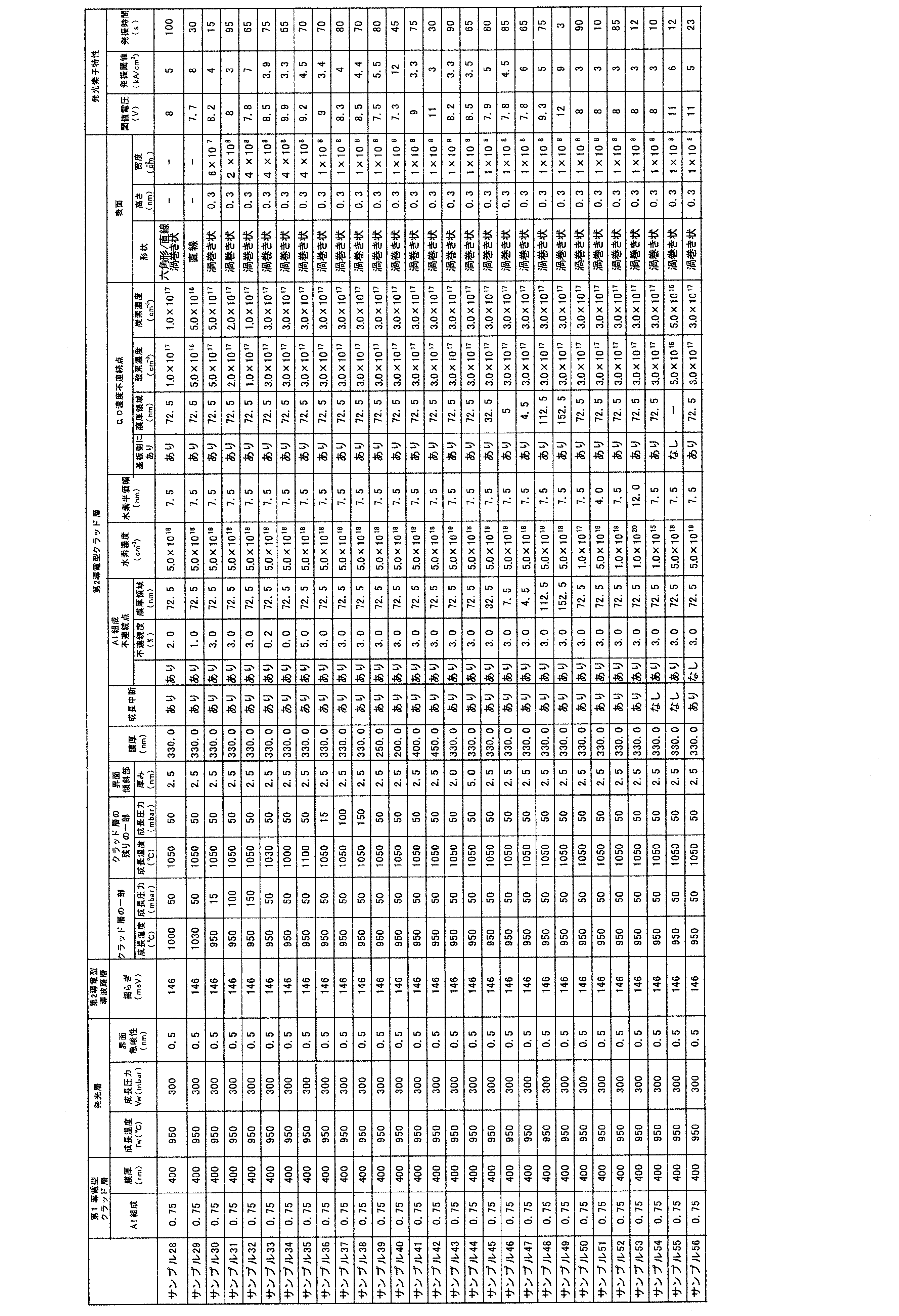
4 発光素子
10 半導体積層部
11 基板
12 バッファ層
13 第1電極
14 第2電極
101 第1導電型クラッド層
102 第1導電型導波路層
103 発光層
104 第2導電型導波路層
105 第2導電型クラッド層
106 コンタクト層
Claims (16)
- Alを含む窒化物半導体基板上に、第1導電型の窒化物半導体を含む第1導電型クラッド層を形成し、
前記第1導電型クラッド層上に、一つ以上の量子井戸を含む窒化物半導体により発光層を形成し、
ウエハ温度が900℃以上1000℃以下であり、リアクタ圧力が15mbar以上350mbar以下の条件で、第2導電型の窒化物半導体を含む第2導電型クラッド層の一部を形成し、
前記ウエハ温度が1030℃以上1100℃以下であり、リアクタ圧力が15mbar以上350mbar以下の条件で前記第2導電型クラッド層の残りの一部を形成して、前記窒化物半導体基板上に半導体積層部を形成する窒化物半導体積層体の製造方法。 - 前記第2導電型クラッド層の一部を形成する際の前記リアクタ圧力が15mbar以上100mbar以下である請求項1に記載の窒化物半導体積層体の製造方法。
- 前記第1導電型クラッド層、前記発光層及び前記第2導電型クラッド層の形成時に、有機金属ガスを流入させ、
前記発光層を形成した後、前記第2導電型クラッド層の一部を形成する前に前記有機金属ガスの流入を一時的に停止させ、
前記第2導電型クラッド層の一部を形成した後、前記第2導電型クラッド層の残りの一部を形成する前に、前記有機金属ガスの流入を一時的に停止させる請求項1又は2に記載の窒化物半導体積層体の製造方法。 - 請求項1から3のいずれか一項に記載の窒化物半導体積層体の製造方法により前記半導体積層部を形成したあと、
前記半導体積層部の各層の不要部分をエッチングによって除去し、
前記半導体積層部上に電極を形成し、
前記半導体積層部の角層が形成された前記窒化物半導体基板をダイシングにより個片へと分割する窒化物半導体素子の製造方法。 - Alを含む窒化物半導体基板と、
前記窒化物半導体基板上に配置される半導体積層部と、を備え、
前記半導体積層部は、
第1導電型の窒化物半導体を含む第1導電型クラッド層と、
前記第1導電型クラッド層上に配置され、一つ以上の量子井戸を含む窒化物半導体で形成された発光層と、
前記発光層上に配置され、第2導電型のAlを含む窒化物半導体で形成された第2導電型クラッド層と、を有し、
前記第2導電型クラッド層の表面は、平面視で直線状以外のテラスと段差とを有する渦巻き状のステップテラス構造を有している窒化物半導体素子。 - 前記渦巻き状のステップテラス構造の高さは、0.2nm以上0.4nm以下である請求項5に記載の窒化物半導体素子。
- 前記渦巻き状のステップテラス構造の分布密度は、1×107cm-2以上5×108cm-2以下である請求項5に記載の窒化物半導体素子。
- 前記窒化物半導体基板は、AlN単結晶基板である請求項5に記載の窒化物半導体素子。
- 前記第1導電型クラッド層は、AlaGa(1-a)N(0.65<a≦0.9)で形成されている請求項5に記載の窒化物半導体素子。
- 前記第1導電型クラッド層の厚さは、250nm以上800nm以下である、請求項5に記載の窒化物半導体素子。
- 前記第1導電型クラッド層と前記発光層との間に配置されて、前記発光層へ光を閉じ込める第1導電型導波路層と、
前記第2導電型クラッド層と前記発光層との間に配置されて、前記発光層へ光を閉じ込める第2導電型導波路層と、を備える、請求項5に記載の窒化物半導体素子。 - 前記第2導電型クラッド層上に配置され、GaNを含む窒化物半導体で形成された第2導電型コンタクト層を備え、
前記第2導電型クラッド層は、AldGa(1-d)N(0.1≦d≦1)を含み、前記窒化物半導体基板から遠ざかるにつれてAl組成dが小さくなる組成傾斜を有し、膜厚が500nm以下である請求項5に記載の窒化物半導体素子。 - 前記第2導電型クラッド層は、前記窒化物半導体基板側から遠ざかるにつれて前記Al組成dが1から0.7の範囲で減少する組成傾斜を有する請求項12に記載の窒化物半導体素子。
- 前記第2導電型クラッド層の膜厚は250nm以上400nm以下である請求項12又は9に記載の窒化物半導体素子。
- 前記第1導電型クラッド層の膜厚T0は、3300×a-2100nm以上15700×a-10100nm以下(aは、前記第1導電型クラッド層を構成する窒化物半導体のIII族原子の合計を1としたときのAl原子の割合)である請求項5に記載の窒化物半導体素子。
- 前記第1導電型クラッド層の抵抗率は、1×10⁻³Ωcm以上5×10⁻³Ωcm以下である請求項15に記載の窒化物半導体素子。
Priority Applications (3)
| Application Number | Priority Date | Filing Date | Title |
|---|---|---|---|
| JP2025511219A JPWO2024204635A1 (ja) | 2023-03-30 | 2024-03-28 | |
| CN202480023314.5A CN121058136A (zh) | 2023-03-30 | 2024-03-28 | 氮化物半导体层叠体和氮化物半导体元件的制造方法以及氮化物半导体元件 |
| DE112024001497.6T DE112024001497T5 (de) | 2023-03-30 | 2024-03-28 | Verfahren zum herstellen eines nitridhalbleiterstapels und nitridhalbleiterelements und nitridhalbleiterelement |
Applications Claiming Priority (2)
| Application Number | Priority Date | Filing Date | Title |
|---|---|---|---|
| JP2023-056152 | 2023-03-30 | ||
| JP2023056152 | 2023-03-30 |
Publications (1)
| Publication Number | Publication Date |
|---|---|
| WO2024204635A1 true WO2024204635A1 (ja) | 2024-10-03 |
Family
ID=92906867
Family Applications (1)
| Application Number | Title | Priority Date | Filing Date |
|---|---|---|---|
| PCT/JP2024/012872 Ceased WO2024204635A1 (ja) | 2023-03-30 | 2024-03-28 | 窒化物半導体積層体及び窒化物半導体素子の製造方法、並びに窒化物半導体素子 |
Country Status (4)
| Country | Link |
|---|---|
| JP (1) | JPWO2024204635A1 (ja) |
| CN (1) | CN121058136A (ja) |
| DE (1) | DE112024001497T5 (ja) |
| WO (1) | WO2024204635A1 (ja) |
Citations (3)
| Publication number | Priority date | Publication date | Assignee | Title |
|---|---|---|---|---|
| JP2009231745A (ja) * | 2008-03-25 | 2009-10-08 | Showa Denko Kk | Iii族窒化物半導体発光素子、iii族窒化物半導体発光素子の製造方法、及びランプ |
| WO2020121794A1 (ja) * | 2018-12-11 | 2020-06-18 | パナソニックセミコンダクターソリューションズ株式会社 | 窒化物系半導体発光素子及びその製造方法、並びに、窒化物系半導体結晶の製造方法 |
| WO2021090849A1 (ja) * | 2019-11-08 | 2021-05-14 | ヌヴォトンテクノロジージャパン株式会社 | 半導体発光素子、及び半導体発光素子の製造方法 |
-
2024
- 2024-03-28 WO PCT/JP2024/012872 patent/WO2024204635A1/ja not_active Ceased
- 2024-03-28 CN CN202480023314.5A patent/CN121058136A/zh active Pending
- 2024-03-28 JP JP2025511219A patent/JPWO2024204635A1/ja active Pending
- 2024-03-28 DE DE112024001497.6T patent/DE112024001497T5/de active Pending
Patent Citations (3)
| Publication number | Priority date | Publication date | Assignee | Title |
|---|---|---|---|---|
| JP2009231745A (ja) * | 2008-03-25 | 2009-10-08 | Showa Denko Kk | Iii族窒化物半導体発光素子、iii族窒化物半導体発光素子の製造方法、及びランプ |
| WO2020121794A1 (ja) * | 2018-12-11 | 2020-06-18 | パナソニックセミコンダクターソリューションズ株式会社 | 窒化物系半導体発光素子及びその製造方法、並びに、窒化物系半導体結晶の製造方法 |
| WO2021090849A1 (ja) * | 2019-11-08 | 2021-05-14 | ヌヴォトンテクノロジージャパン株式会社 | 半導体発光素子、及び半導体発光素子の製造方法 |
Also Published As
| Publication number | Publication date |
|---|---|
| CN121058136A (zh) | 2025-12-02 |
| JPWO2024204635A1 (ja) | 2024-10-03 |
| DE112024001497T5 (de) | 2026-03-05 |
Similar Documents
| Publication | Publication Date | Title |
|---|---|---|
| JP7560296B2 (ja) | 紫外線発光素子 | |
| JP2019110195A (ja) | 窒化物半導体発光素子 | |
| JP2020167321A (ja) | 窒化物半導体発光素子 | |
| JP7589940B2 (ja) | レーザダイオードの製造方法およびレーザダイオード | |
| JP7492885B2 (ja) | 紫外線発光素子 | |
| WO2024204634A1 (ja) | 窒化物半導体素子、窒化物半導体積層体の製造方法及び窒化物半導体素子の製造方法 | |
| WO2024204636A1 (ja) | 窒化物半導体素子、窒化物半導体積層体の製造方法、及び窒化物半導体素子の製造方法 | |
| JP2024143457A (ja) | 窒化物半導体素子及び窒化物半導体素子の製造方法 | |
| JP2024143415A (ja) | 窒化物半導体素子及び窒化物半導体素子の製造方法 | |
| JP2024143456A (ja) | 窒化物半導体素子及び窒化物半導体素子の製造方法 | |
| JP2021034509A (ja) | 紫外線発光素子 | |
| JP7825822B2 (ja) | 発光素子の製造方法および発光素子 | |
| JP7646147B2 (ja) | レーザダイオード | |
| JP7594257B2 (ja) | レーザダイオード | |
| JP7614607B2 (ja) | レーザダイオードの製造方法、レーザダイオード | |
| JP2025124236A (ja) | レーザダイオード | |
| JP7489269B2 (ja) | 紫外線発光素子 | |
| WO2023163230A1 (ja) | レーザダイオード | |
| JP2025126648A (ja) | 半導体デバイスの製造方法及び半導体デバイス | |
| JP7388859B2 (ja) | 窒化物半導体素子 | |
| JP2023125769A (ja) | レーザダイオード | |
| WO2024047917A1 (ja) | レーザダイオード | |
| CN121058136A (zh) | 氮化物半导体层叠体和氮化物半导体元件的制造方法以及氮化物半导体元件 | |
| JP7405554B2 (ja) | 紫外線発光素子 | |
| JP7678426B2 (ja) | 光デバイス |
Legal Events
| Date | Code | Title | Description |
|---|---|---|---|
| 121 | Ep: the epo has been informed by wipo that ep was designated in this application |
Ref document number: 24780733 Country of ref document: EP Kind code of ref document: A1 |
|
| ENP | Entry into the national phase |
Ref document number: 2025511219 Country of ref document: JP Kind code of ref document: A |
|
| WWE | Wipo information: entry into national phase |
Ref document number: 2025511219 Country of ref document: JP |
|
| WWE | Wipo information: entry into national phase |
Ref document number: 112024001497 Country of ref document: DE |
|
| WWP | Wipo information: published in national office |
Ref document number: 112024001497 Country of ref document: DE |
|
| 122 | Ep: pct application non-entry in european phase |
Ref document number: 24780733 Country of ref document: EP Kind code of ref document: A1 |