WO2024204632A1 - リフレクタ - Google Patents
リフレクタ Download PDFInfo
- Publication number
- WO2024204632A1 WO2024204632A1 PCT/JP2024/012860 JP2024012860W WO2024204632A1 WO 2024204632 A1 WO2024204632 A1 WO 2024204632A1 JP 2024012860 W JP2024012860 W JP 2024012860W WO 2024204632 A1 WO2024204632 A1 WO 2024204632A1
- Authority
- WO
- WIPO (PCT)
- Prior art keywords
- reflector
- conductor pattern
- reflection
- dielectric layer
- ghz
- Prior art date
- Legal status (The legal status is an assumption and is not a legal conclusion. Google has not performed a legal analysis and makes no representation as to the accuracy of the status listed.)
- Ceased
Links
Images


Classifications
-
- H—ELECTRICITY
- H01—ELECTRIC ELEMENTS
- H01Q—ANTENNAS, i.e. RADIO AERIALS
- H01Q15/00—Devices for reflection, refraction, diffraction or polarisation of waves radiated from an antenna, e.g. quasi-optical devices
- H01Q15/14—Reflecting surfaces; Equivalent structures
- H01Q15/148—Reflecting surfaces; Equivalent structures with means for varying the reflecting properties
-
- H—ELECTRICITY
- H01—ELECTRIC ELEMENTS
- H01Q—ANTENNAS, i.e. RADIO AERIALS
- H01Q15/00—Devices for reflection, refraction, diffraction or polarisation of waves radiated from an antenna, e.g. quasi-optical devices
- H01Q15/0006—Devices acting selectively as reflecting surface, as diffracting or as refracting device, e.g. frequency filtering or angular spatial filtering devices
- H01Q15/0086—Devices acting selectively as reflecting surface, as diffracting or as refracting device, e.g. frequency filtering or angular spatial filtering devices said selective devices having materials with a synthesized negative refractive index, e.g. metamaterials or left-handed materials
-
- H—ELECTRICITY
- H01—ELECTRIC ELEMENTS
- H01Q—ANTENNAS, i.e. RADIO AERIALS
- H01Q15/00—Devices for reflection, refraction, diffraction or polarisation of waves radiated from an antenna, e.g. quasi-optical devices
- H01Q15/14—Reflecting surfaces; Equivalent structures
Definitions
- the present invention relates to a reflector, and in particular to a reflector having a metasurface.
- high-frequency radio waves such as microwaves, millimeter waves, and terahertz waves in wireless communication enables high-speed, high-capacity communication.
- high-frequency radio waves such as 1 GHz to 10 THz have a tendency to travel in a very straight line, and the presence of an obstacle between the transmitting antenna and the receiving antenna means that the radio waves cannot reach the desired location, making communication impossible.
- Reflectors are used to improve the communication environment and communication area of mobile communications using high frequencies. Conventional reflectors have a specular reflective surface with an equal angle of incidence and reflection, so there is a limit to the reflection range. In order to expand the communication range, metareflectors with metasurfaces that reflect incident waves in the desired direction are being actively developed.
- Metal surface refers to an artificial surface that controls the transmission and reflection characteristics of incident electromagnetic waves. Metal patterns of about half the wavelength are arranged periodically, and the reflection characteristics are controlled to reflect the incident wave in the desired direction.
- a reflectarray has been proposed in which array elements are formed in divided areas on a substrate, and the gaps between the multiple patches that make up the array elements are different for each area (see, for example, Patent Document 1).
- reflectarrays with metasurfaces utilize the resonance phenomenon, when reflecting in a desired direction (hereafter also referred to as the "target direction") at a specified frequency, the reflection distance to the target and the beam diameter are inversely proportional. Therefore, as the reflection distance increases, there is a problem in that the beam diameter of the main lobe of the reflected wave in the target direction narrows. When the main lobe beam diameter narrows, the coverage area within the space within the reach of the radio waves is limited, and communication may become impossible.
- the present invention aims to provide a reflector that increases the beam diameter of the main lobe of the reflected wave toward the target.
- the reflector has a dielectric layer, a conductive layer formed on a first surface of the dielectric layer and including a plurality of conductor patterns that reflect an incident wave, and a ground layer formed on a second surface of the dielectric layer opposite the first surface, the conductor patterns are arranged in a predetermined direction, and among the plurality of conductor patterns, the standard deviation ⁇ of the difference between the center-to-center distance between a reference conductor pattern and an arbitrary conductor pattern and the ideal distance along the predetermined direction is 0.5 mm or more and 1.5 mm or less.
- the above configuration realizes a reflector that increases the beam diameter of the main lobe of the reflected wave toward the target.
- FIG. 2 is a diagram showing a basic configuration of a reflector according to the first embodiment.
- FIG. 13 is a diagram illustrating an example of a method for designing a conductor pattern.
- 4A to 4C are diagrams illustrating a design example of a reflector according to the first embodiment.
- 4A to 4C are diagrams illustrating a design example of a reflector according to the first embodiment.
- FIG. 4 is a diagram showing the reflection characteristics of a reflector according to the design of FIGS. 3A and 3B.
- FIG. 1 is a diagram showing the configuration of standard deviations in Examples and Comparative Examples.
- FIG. 6 is a diagram showing the reflection characteristics of the reflector designed in FIG. 5 .
- FIG. 6 is a diagram showing the reflection characteristics of the reflector designed in FIG. 5 .
- FIG. 2 is a diagram showing the reflection characteristics of a low dielectric constant reflector.
- FIG. 2 is a diagram showing the reflection characteristics of a low dielectric constant reflector.
- FIG. 2 is a diagram showing the reflection characteristics of a low dielectric constant reflector.
- FIG. 2 is a diagram showing the reflection characteristics of a high dielectric constant reflector.
- FIG. 2 is a diagram showing the reflection characteristics of a high dielectric constant reflector.
- FIG. 1 is a diagram showing the reflection range of a low dielectric constant reflector versus frequency.
- FIG. 2 is a diagram showing the reflection range of a high dielectric constant reflector versus frequency.
- FIG. 1 is a diagram showing the reflection range of a low dielectric constant reflector versus frequency.
- FIG. 1 is a diagram showing the relationship between the thickness of dielectric layers with different dielectric constants and the reflection bandwidth.
- FIG. 13 is a diagram showing the relationship between the thickness of dielectric layers having different dielectric constants and the reflection intensity.
- FIG. 2 is a diagram showing the configurations and characteristics of an example and a comparative example.
- FIG. 11 is a schematic diagram of a reflector according to a second embodiment.
- FIG. 13 is a diagram showing the results of a simulation in which the thickness and dielectric constant of a protective layer are changed.
- 1A and 1B are diagrams illustrating examples of use of a reflector according to an embodiment.
- FIG. 1 is a diagram showing an example of use of a normal reflector.
- the reflector 10 has a dielectric layer 11, a conductive layer 13 provided on a first surface 111 of the dielectric layer 11, and a ground layer 12 provided on a second surface 112 opposite to the first surface 111 of the dielectric layer 11.
- the conductive layer 13 includes an array of multiple conductor patterns 131 and functions as a reflecting surface of the reflector 10. This reflecting surface is a metasurface that reflects an incident wave at an angle (absolute value) different from the incident angle.
- the ground layer 12 forms a capacitance between the ground layer 12 and each conductor pattern 131, and the magnitude of the phase delay can be controlled for each conductor pattern 131.
- the conductive layer 13 and the ground layer 12 are not particularly limited as long as they are made of a material having electrical conductivity, but copper foil is preferable in terms of electrical conductivity, manufacturability, processability, material price, etc.
- the size and pitch of the conductor patterns 131 are set according to the desired reflection characteristics.
- Each conductor pattern 131 has a size sufficiently smaller than the wavelength used, and selectively reflects radio waves in the desired frequency band.
- the conductor patterns 131 control the phase of the reflection, and the reflected waves are superimposed to form a reflected beam BM in the desired direction.
- the wavelength of the incident radio wave is ⁇
- the pitch of the conductor pattern 131 i.e., the distance between the centers of adjacent conductor patterns 131
- the phases of the radio waves reflected by two adjacent conductor patterns 131 are ⁇ 1 and ⁇ 2, respectively
- the reflection angle is ⁇ .
- the phase difference ⁇ 1- ⁇ 2 is expressed by equation (1).
- n is an integer.
- ⁇ 1, ⁇ 2, and d may be designed so as to obtain the desired reflection angle ⁇ .
- the reflection angle ⁇ is set to a desired angle between the normal direction (0°) of the reflecting surface of the reflector 10 and the horizontal direction (90°), excluding 0° and 90°.
- the values of ⁇ 1 and ⁇ 2, which represent the reflection phase, can be controlled and changed by design parameters such as the wavelength ⁇ of the incident radio wave, the size (length x width) and pitch of the conductor pattern 131, and the thickness and dielectric constant of the reflector 10.
- the conductor pattern 131 may be designed by creating a graph of the length/phase characteristics shown in FIG. 2.
- the length/phase characteristics in FIG. 2 can be obtained by measuring the reflection pattern of the radio waves while changing the length L of the conductor pattern with the design parameters other than the length L (mm) fixed, and analyzing it using three-dimensional electromagnetic field simulation software.
- Length L is the length of conductor pattern 131 corresponding to the vibration direction of the radio wave, and as shown in Figure 3A, when conductor patterns 131a to 131g are cross patterns, each conductor pattern has the same vertical and horizontal lengths.
- a plurality of conductor patterns 131 of different sizes are arranged at a predetermined distance apart.
- the conductor patterns 131 are arranged in a line on a straight line l.
- the center points of the conductor patterns 131 are located on an arbitrary straight line.
- the conductor patterns 131 do not have to be arranged in a straight line, and may be arranged in a staggered pattern or other arrangement patterns in the arrangement direction.
- the "center point of a conductor pattern” means the center point of a circle inscribed in the contour of each conductor pattern when the conductor pattern is viewed in a plane.
- the distance between the center point of a reference conductor pattern and an arbitrary conductor pattern is called the "center-to-center distance".
- the center-to-center distance from the center point of the reference conductor pattern to the center point of the m-th conductor pattern counted from the reference conductor pattern may be expressed as "dm” or "dm'” using an arbitrary integer m of 1 or more.
- the first conductor pattern 131a from the left in FIG. 3A is taken as the reference conductor pattern, and the center-to-center distance of the first conductor pattern (the second conductor pattern 131b from the left in FIG.
- the ideal distance is represented as dm.
- the center-to-center distance between the first conductor pattern and the m-th conductor pattern formed on the first surface of the dielectric layer is defined as the "actual distance" of the m-th conductor pattern with respect to the ideal distance dm. In this specification, the actual distance is denoted as dm'.
- the absolute value of the difference between the actual distance dm′ and the ideal distance dm is
- of each conductor pattern other than the reference conductor pattern is 0.5 mm or more and 1.5 mm or less.
- the "beam diameter” is defined as the reflection angle range where the difference in intensity ⁇ from the peak intensity is 10 dB when the intensity distribution of the main lobe of the reflected wave is graphed with the reflection angle on the horizontal axis and the reflected wave intensity on the vertical axis.
- the reflector has a dielectric layer 11 with a relative dielectric constant of 2.0 or less.
- the frequency band of radio waves that are reflected in a predetermined direction can be expanded. Details of expanding the reflection frequency band will be described later with reference to FIG. 5 and subsequent figures.
- a dielectric material with a relative dielectric constant of 2.0 or less a fluorinated resin such as polytetrafluoroethylene, a combination of a fluorinated resin and an inorganic porous aggregate, other transparent porous resins, and the like can be used.
- a resin that is combined with the inorganic porous aggregate polytetrafluoroethylene, polystyrene, and the like are used.
- the inorganic porous aggregate is produced, for example, by the method described in JP 2017-171898 A.
- Figures 3A and 3B show a design example of the reflector 10 of the first embodiment.
- Figure 3A shows the arrangement of the conductor patterns 131a to 131h that make up the conductive layer 13.
- Figure 3B shows the size of each conductor pattern.
- the conductor patterns 131a to 131h are cross patterns with equal vertical and horizontal lengths.
- the size of each conductor pattern 131 is shown by the vertical or horizontal length L1 to L8.
- the incident wave has a wavelength ⁇ of 10.8 mm in the 28 GHz band, and the pitch of the conductor patterns 131a to 131h, i.e., the ideal center-to-center distance dm, is 5.35 mm for all of them.
- the arrangement of conductor patterns 131a to 131h aims for a reflection angle of -42°.
- the reflection angle in this case is the reflection angle when radio waves are incident perpendicularly on reflector 10, that is, the reflection angle with respect to the normal. If we calculate the phase difference " ⁇ 1 - ⁇ 2" when ⁇ is -42° based on the above formula (1), the phase difference is 120°.
- the size of conductor patterns 131a to 131h, that is, the lengths L1 to L8, are determined so that this phase difference can be obtained.
- the shape of the conductor pattern 131 is not limited to a cross pattern, and may be circles, ellipses, polygons, etc. of different sizes arranged at a predetermined period.
- the size of the conductor pattern 131 is preferably 2.0 to 5.0 mm long, but the size of the conductor pattern 131 is appropriately designed according to the frequency band. Radio waves of a frequency determined by the size and period of the conductor pattern 131 are selectively reflected.
- the frequency band selected by resonance is narrow, but by setting the relative dielectric constant of the dielectric layer 11 to 2.0 or less, the selected frequency band can be expanded to a bandwidth of 4 GHz or more, more preferably 6 GHz or more.
- the selected frequency bandwidth can change depending on the thickness of the dielectric layer 11 of the reflector 10, so a wideband reflector with a bandwidth per unit thickness (1 mm) of the reflector 10 exceeding 6.5 GHz/mm is realized.
- Figure 4 shows the reflection characteristics of the reflector 10 by Ref, designed in such a way that the standard deviation ⁇ of the absolute value of the difference between the actual distance dm' and the ideal distance dm,
- the horizontal axis is the reflection angle
- the vertical axis is the reflection intensity (dB).
- the main peak was observed in the -42° direction, and it was confirmed that the reflector 10 was able to control the reflection direction of the radio waves almost exactly as designed.
- the reflection intensity was analyzed by using Dassault Systèmes CST Studio Suite, which is a general-purpose three-dimensional electromagnetic field simulation software, and the reflection intensity for each angle was analyzed.
- the angle at which the reflection intensity peak appears is defined as the "reflection peak angle.”
- the reflection peak angle and beam diameter were evaluated as follows.
- ⁇ The beam diameter is larger than that of the REF, and the difference in the reflection peak angle with respect to the reflection peak angle of the REF is within ⁇ 2°.
- ⁇ The beam diameter is larger than that of the REF, but the reflection peak angle is shifted.
- ⁇ The beam diameter is smaller than that of the REF.
- the simulation results of the reflection characteristics of the reflector designed in Figure 5 are shown in Figures 6 and 7.
- the vertical axis of Figure 6 is the reflection intensity (unit: dB), and the horizontal axis is the reflection angle (unit: °).
- Figures 8A to 8C show the reflection characteristics of a low dielectric constant reflector for incident waves of different frequencies.
- the low dielectric constant reflector is a reflector of the embodiment, which is a reflector 10 using a dielectric layer 11 with a relative dielectric constant of 2.0 or less. In this example, a dielectric layer with a relative dielectric constant ⁇ of 1.88 is used.
- Figures 9A to 9C show the reflection characteristics of a high dielectric constant reflector for incident waves of different frequencies.
- the high dielectric constant reflector is a reflector using a dielectric layer with a relative dielectric constant exceeding 2.0.
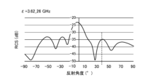
- the reflection spectra of 26 GHz, 28 GHz, and 31 GHz are calculated using a dielectric layer 11 with a relative dielectric constant ⁇ of 1.88.
- the reflection intensity on the vertical axis is shown as the scattering cross section (RCS: Radar Cross Section), which is an index of reflection ability.
- RCS Radar Cross Section
- Plane waves in the frequency bands of 26 GHz, 28 GHz, and 31 GHz are incident from the normal direction of the reflector, and the scattering cross section is analyzed for each angle using Dassault Systèmes CST Studio Suite, a general-purpose 3D electromagnetic field simulation software.
- ⁇ 1.88
- a peak appears in the reflection spectrum at a direction of 35° at all frequencies: 26 GHz, 28 GHz, and 31 GHz.
- the peak value is within the range of -25 dB ⁇ 2.5 dB, and a stable peak intensity is obtained at a target reflection angle of 35° over at least a 5 GHz frequency band.
- the main lobe with a reflection angle of 35° is clearly distinguished from the other side lobes, and it can be seen that the incident wave is reflected with good control in the targeted 35° direction.
- other peaks appear at 0° and -65°.
- the 0° peak is a reflection in the same direction as the incident wave, so it represents a loss.
- the -65° peak is a reflection in the opposite direction to the target 35°, and depending on the environment in which the reflector is used, this may result in a loss, or it may be an advantage in that it delivers radio waves in two directions at once.
- the relative dielectric constant ⁇ is changed to 3.62, and other conditions such as the conductor pattern are maintained the same as those of the reflector of Figures 8A to 8C.
- Materials with a relative dielectric constant of 3.62 include polyphenylene ether (PPE) and acrylic resin.
- Figures 9A to 9C directly represent the fact that in a metasurface that utilizes resonance, the reflection characteristics deteriorate as the frequency changes.
- the frequency characteristics are greatly improved.
- the frequency band of reflection can be expanded by lowering the dielectric constant of the dielectric layer 11 used in the reflector 10 to a certain extent.
- Figure 10A shows the reflection range of a low dielectric constant reflector
- Figure 10B shows the reflection range of a high dielectric constant reflector.
- the horizontal axis is the reflection angle
- the vertical axis is the frequency of the incident wave.
- the reflector model used has the same conductor pattern as Figure 3A formed on the surface of the dielectric layer.
- the relative dielectric constant ⁇ of the low dielectric constant reflector in Figure 10A is set to 1.88
- the relative dielectric constant ⁇ of the high dielectric constant reflector in Figure 10B is set to 3.62.
- a high reflection intensity (greater than -30 dB and less than -20 dB) is obtained from 24 GHz to 33 GHz.
- This reflection intensity is distributed in a range of ⁇ 10° from 35°, and in particular, in the range of 23° to 35°, a reflection intensity of greater than -30 dB and less than -20 dB is obtained over a frequency band of 10 GHz or more.
- the wide range of reflection frequency characteristics realizes high resistance to environmental changes.
- Fig. 11 shows the relationship between the thickness of the dielectric layer with different dielectric constants and the frequency band of reflection.
- Fig. 12 shows the relationship between the thickness of the dielectric layer with different dielectric constants and the reflection intensity.
- the thickness of the dielectric layer 11 is changed to 0.30 mm, 0.50 mm, and 0.75 mm.
- the conductor pattern 131 formed on the first surface 111 of the dielectric layer 11 is the same as that in Fig. 3A.
- the pattern configuration of the conductor is the same, but the relative dielectric constant ⁇ of the dielectric layer 11 is made different.
- a plane wave of 28 GHz is incident from the normal direction of the reflector, and the frequency band of reflection is analyzed.
- the bandwidth of the reflected wave is the frequency bandwidth attenuated by 3 dB from the peak value of the main lobe of the reflection.
- the thickness of the dielectric layer 11 When the thickness of the dielectric layer 11 is the same, the lower the relative dielectric constant ⁇ , the wider the reflection frequency band. Conversely, when realizing the same reflection frequency band, a material with a lower dielectric constant allows the reflector to be formed thinner.
- a reflector with ⁇ of 1.88 achieves a reflection frequency band exceeding 6.5 GHz, but a reflector with ⁇ of 3.62 can only cover a reflection frequency band of 4.5 GHz.
- the reflection frequency band As mentioned above, considering the frequency bands and peak shifts used in each country, it is desirable for the reflection frequency band to exceed 6 GHz in the frequency band between 24 GHz and 30 GHz. Interpolating the data points in Figure 11, it may be possible to achieve a reflection frequency band of 6 GHz by increasing the thickness of the dielectric layer 11, which has an ⁇ of 3.62, to about 1.2 m. However, in that case, the reflector will become thicker, reducing flexibility and limiting the range of application.
- the thickness of the dielectric layer 11 is changed to 0.25 mm, 0.30 mm, 0.50 mm, and 0.80 mm, and the peak intensity of the reflected wave is calculated.
- the relative dielectric constant ⁇ is 1.88
- a peak intensity exceeding -24 dB can be obtained by making the thickness of the dielectric layer 11 0.30 mm or more.
- ⁇ is 3.62
- the thickness of the dielectric layer 11 must be 0.5 mm to obtain the same level of peak intensity.
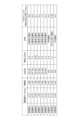
- FIG. 13 shows the configurations and characteristics of the examples and comparative examples.
- the configuration parameters are the type, thickness, relative dielectric constant, and porosity of the base material that constitutes the dielectric layer 11. The values of these parameters are variously changed.
- the reflector characteristics are the frequency band of reflection and the band per unit thickness.
- the conductor patterns 131 are the conductor patterns 131a to 131h in FIG. 3A, and the type and parameters of the dielectric layer 11 are changed.
- Wavelength of incident wave 10.7 mm (frequency 28 GHz) Incident wave frequency change range: 20 GHz to 35 GHz Incident angle of incident wave with respect to the normal direction of the reflector: 0 degrees
- First desired reflection angle ⁇ of the reflection spectrum with respect to the normal direction of the reflector 35 degrees
- Example 4 a fluorine porous substrate is used as the base material of the dielectric layer 11.
- the fluorine porous substrate is a combination of a fluorinated resin and an inorganic porous aggregate. Polytetrafluoroethylene is used as the fluorinated resin.
- the thickness of this dielectric substrate is 0.75 mm, the porosity is 33.2%, and the relative dielectric constant is 1.88.
- the reflection frequency band of the reflector obtained in Example 1 is 6.6 GHz, and the band per unit thickness (1 mm) is 8.8 GHz/mm.
- Example 5 In Example 5, a fluorine porous substrate is used as the base material of the dielectric layer 11.
- the thickness of this dielectric substrate is 0.75 mm, the porosity is 67.7%, and the relative dielectric constant is 1.50.
- the dielectric layer 11 is designed to have different porosities and relative dielectric constants by changing the aggregation density of the porous inorganic fine particles used in the fluorine porous substrate.
- the reflection frequency band of the reflector obtained in Example 5 is 7.1 GHz, and the band per unit thickness (1 mm) is 9.5 GHz/mm.
- Example 6 In Example 6, a fluorine porous substrate is used as the base material of the dielectric layer 11.
- the thickness of this dielectric substrate is 0.50 mm, the porosity is 33.0%, and the relative dielectric constant is 1.88.
- the dielectric layer 11 is designed to have a different porosity and relative dielectric constant by changing the aggregation density of the porous inorganic fine particles used in the fluorine porous substrate.
- the dielectric layer 11 is thinner than in Examples 4 and 5.
- the reflection frequency band of the reflector obtained in Example 6 is 4.55 GHz, and the band per unit thickness (1 mm) is 9.1 GHz/mm.
- Example 8 In Example 8, a fluorine porous substrate is used as the base material of the dielectric layer 11. The thickness of this dielectric substrate is 0.75 mm, the porosity is 22.5%, and the relative dielectric constant is 2.00. The aggregation density of the porous inorganic fine particles used in the fluorine porous substrate is controlled to design different porosities and relative dielectric constants.
- the reflection frequency band of the reflector obtained in Example 8 is 5.5 GHz, and the band per unit thickness (1 mm) is 7.3 GHz/mm.
- Example 9 a fluorine porous substrate is used as the base material of the dielectric layer 11.
- This dielectric base material has a thickness of 0.3 mm, a porosity of 33.0%, and a relative dielectric constant of 1.88.
- the thickness of the dielectric layer 11 is made thinner than that of Example 8.
- the reflection frequency band of the reflector obtained in Example 9 is 4.1 GHz, and the band per unit thickness (1 mm) is 13.7 GHz.
- Comparative Example 7 PPE is used as the substrate of the dielectric layer 11.
- the thickness of the PPE substrate is 0.75 mm, the porosity is 0.0%, and the relative dielectric constant is 3.62.
- the reflection frequency band of the reflector obtained in Comparative Example 7 is 4.5 GHz, and the band per unit thickness (1 mm) is 6.0 GHz/mm.
- the relative dielectric constant is high, and therefore the reflection frequency band is narrower.
- Comparative Example 8 a glass epoxy base material is used as the base material of the dielectric layer 11.
- This dielectric base material has a thickness of 0.75 mm, a porosity of 0.0%, and a relative dielectric constant of 5.00.
- the relative dielectric constant is higher than that of Comparative Example 7.
- the reflection frequency band of the reflector obtained in Comparative Example 8 is 3.7 GHz, and the band per unit thickness (1 mm) is 4.9 GHz/mm.
- the dielectric constant of the dielectric layer 11 is 2.0 or less, a wideband reflection characteristic exceeding 6.5 GHz, preferably exceeding 7.0 GHz, and more preferably exceeding 8.0 GHz per unit thickness of the reflector can be obtained.
- the thickness of the dielectric layer is thin and the dielectric constant is 1.88 or less, a frequency band of 8.8 GHz or more per unit thickness of the reflector is realized.
- a dielectric constant of 2.0 or less can be achieved with a porosity of about 20% for the dielectric layer 11.
- the thickness of the dielectric layer 11 can be designed appropriately depending on the application.
- the thickness of the dielectric layer 11 may be 0.3 mm or more and 1.0 mm or less. By making the thickness of the dielectric layer 11 0.3 mm or more, a highly robust reflector 10 can be obtained. Furthermore, if the thickness of the dielectric layer 11 is 1.0 mm or less, it is advantageous for reducing the weight in the design of a large reflector with a side length of about 1 m, and is excellent in terms of ease of construction and construction costs. Note that when the thickness is 0.3 mm, 1.0 mm, etc., it is assumed that the allowable manufacturing error is included.
- FIG. 14 is a schematic diagram of the reflector 20 of the second embodiment.
- the main parts of the reflector 20 are the same as those of the reflector 10 of the first embodiment, and a dielectric layer 21 with a relative dielectric constant of 2.0 or less is used.
- a conductive layer 23 including a predetermined conductor pattern 231 is formed on the first surface 211 of the dielectric layer 21, and a ground layer 22 is provided on the second surface 212.
- the conductor pattern 231 is designed so that the reflection direction of the main lobe for an incident wave in the 28 GHz band is tilted at a predetermined angle from the normal direction, and an example of this is the pattern shown in FIG. 3A. Below, the design was changed so that the target value of the reflection peak angle was set to "-43°", and analysis and evaluation were performed by simulation.
- a protective layer 24 is provided covering the conductive layer 23.
- An adhesive layer 26 is provided on the side of the ground layer 22.
- the adhesive layer 26 allows the reflector 20 to be attached to a desired location, such as a wall or ceiling.
- the protective layer 24 is transparent to incident waves of 24 GHz to 30 GHz. Transparent to incident waves means that the transmittance of the incident waves is 60% or more, preferably 70% or more, more preferably 80% or more, and even more preferably 90% or more.
- the protective layer 24 may be transparent to visible light.
- the protective layer 24 protects the conductor pattern 231 of the reflector 20 from deterioration or damage due to external factors, and provides excellent durability.
- the conductor pattern 231 of the reflector 20 is subject to oxidation deterioration over time due to contact with oxygen and moisture in the atmosphere, and the formation of the protective layer 24 is preferable from the viewpoint of weather resistance, particularly when used outdoors. Even indoors, the formation of the protective layer 24 is similarly preferable if the installation environment is one in which condensation is likely to occur.
- the protective layer 24 preferably has a thickness of 0.1 mm or more and 1.0 mm or less, and a relative dielectric constant of 2.0 or less.
- Conductor pattern pitch 5.35 mm
- Relative dielectric constant of protective layer 24 1.0 (Ref), 1.5, 2.0, 3.0, 5.0
- Thickness of protective layer 24 0.0 mm (Ref), 0.2 mm, 0.5 mm, 1.0 mm
- Five cross patterns of different sizes are used as the shape of the conductor pattern, and the reflection angle and reflection intensity are calculated by changing the thickness and relative dielectric constant of the protective layer 24 covering the conductor pattern.
- FIG. 15 The results of the simulation are shown in FIG. 15.
- "Ref” in the leftmost column of FIG. 15 shows a reference configuration in which the protective layer 24 is not provided.
- the thickness of the protective layer 24 is set to 0.0 mm and the relative dielectric constant is set to 1.0 because an air layer covers the conductor pattern.
- the unit of the reflection intensity of the reference configuration is (dB).
- "Reflection angle deviation” shows the rate of change (%) from the reflection angle of the reference configuration
- “reflection intensity loss” shows the rate of decrease (%) from the reflection intensity of the reference configuration.
- FIG. 15 shows that when the relative dielectric constant Dk is high, the reflection angle deviation and reflection intensity loss are large, and it is desirable for the relative dielectric constant Dk to be 2.0 or less. When the relative dielectric constant Dk is 1.5 or less, the reflection intensity loss is 5% or less, which is more favorable (evaluated as "S" in Figure 15). When the thickness of the protective layer 24 is large, the reflection angle deviation and reflection intensity loss are large, and it is desirable for the thickness of the protective layer 24 to be 0.1 mm or more and 1.0 mm or less.
- FIG. 16A shows an example of how the reflector 20 of the embodiment is used.
- FIG. 16B shows a comparison of an example of how a normal reflector is used.
- FIG. 16A shows how the reflector 10 or 20 of the embodiment is used.
- the reflector 10 or 20 of the embodiment is thin and flexible, and can be installed along an L-shaped bent passage, street, hallway, etc.
- a normal reflector RFL with a mirror-like reflective surface reflects perpendicularly incident radio waves back in the direction of incidence. For this reason, the reflector RFL must be installed at an oblique angle to the incident radio waves. If it is placed in a corner as in Figure 16B, the space cannot be used effectively. In contrast, the reflector 10 or 20 of the embodiment can reduce radio wave blind zones without taking up space or compromising the appearance.
- a dielectric layer a conductive layer formed on a first surface of the dielectric layer and including a plurality of conductor patterns that reflect incident waves; a ground layer formed on a second surface of the dielectric layer opposite to the first surface; having The conductor pattern is arranged in a plurality of patterns along a predetermined direction, Among the plurality of conductor patterns, a standard deviation ⁇ of a difference between a center-to-center distance between a reference conductor pattern and an arbitrary conductor pattern and an ideal distance on a straight line along the predetermined direction is 0.5 mm or more and 1.5 mm or less. Reflector.
- the center-to-center distance between the reference conductor pattern and the m-th conductor pattern at which the intensity of the reflected wave is strongest is defined as an ideal distance dm of the m-th conductor pattern
- a center-to-center distance between the reference conductor pattern and the m-th conductor pattern formed on the first surface of the dielectric layer is defined as an actual distance dm′ of the m-th conductor pattern
- the absolute value of the difference between the actual distance dm' and the ideal distance dm is
- of each conductor pattern other than the reference conductor pattern is 0.5 mm or more and 1.5 mm or less.
- Item 2. The reflector according to item 1. (Item 3) an adhesive layer provided on a surface of the ground layer opposite to the dielectric layer; Item 2. The reflector according to item 1, comprising: (Item 4) a protective layer covering the conductive layer; Item 2. The reflector according to item 1, further comprising: (Item 5) The protective layer has a thickness of 0.1 mm or more and 1.0 mm or less and a relative dielectric constant of 2.0 or less. The reflector according to item 4 (item 6) The thickness of the dielectric layer is 0.3 mm or more and 1.0 m or less. Item 2. The reflector according to item 1. (Item 7) The length of the conductor pattern is not less than 2.0 mm and not more than 5.0 mm. Item 2.
- the reflector according to item 1. (Item 8) The frequency band of reflection per unit thickness of the reflector is greater than 6.5 GHz/mm; Item 2. The reflector according to item 1. (Item 9) The dielectric layer is formed of a combination of a fluorinated resin and an inorganic porous aggregate, and the porosity of the dielectric layer is 20% or more. Item 9. The reflector according to any one of items 1 to 8.
Landscapes
- Physics & Mathematics (AREA)
- Electromagnetism (AREA)
- Aerials With Secondary Devices (AREA)
Priority Applications (4)
| Application Number | Priority Date | Filing Date | Title |
|---|---|---|---|
| CN202480019647.0A CN120898328A (zh) | 2023-03-31 | 2024-03-28 | 反射器 |
| EP24780730.8A EP4693745A1 (en) | 2023-03-31 | 2024-03-28 | Reflector |
| KR1020257031116A KR20250153234A (ko) | 2023-03-31 | 2024-03-28 | 리플렉터 |
| JP2025511217A JPWO2024204632A1 (https=) | 2023-03-31 | 2024-03-28 |
Applications Claiming Priority (2)
| Application Number | Priority Date | Filing Date | Title |
|---|---|---|---|
| JP2023-058657 | 2023-03-31 | ||
| JP2023058657 | 2023-03-31 |
Publications (2)
| Publication Number | Publication Date |
|---|---|
| WO2024204632A1 true WO2024204632A1 (ja) | 2024-10-03 |
| WO2024204632A9 WO2024204632A9 (ja) | 2025-04-10 |
Family
ID=92906854
Family Applications (1)
| Application Number | Title | Priority Date | Filing Date |
|---|---|---|---|
| PCT/JP2024/012860 Ceased WO2024204632A1 (ja) | 2023-03-31 | 2024-03-28 | リフレクタ |
Country Status (6)
| Country | Link |
|---|---|
| EP (1) | EP4693745A1 (https=) |
| JP (1) | JPWO2024204632A1 (https=) |
| KR (1) | KR20250153234A (https=) |
| CN (1) | CN120898328A (https=) |
| TW (1) | TW202448022A (https=) |
| WO (1) | WO2024204632A1 (https=) |
Citations (5)
| Publication number | Priority date | Publication date | Assignee | Title |
|---|---|---|---|---|
| JP2009207078A (ja) * | 2008-02-29 | 2009-09-10 | Mitsubishi Electric Corp | 反射板 |
| JP5177708B2 (ja) | 2010-08-27 | 2013-04-10 | 株式会社エヌ・ティ・ティ・ドコモ | リフレクトアレイ |
| JP2013115756A (ja) * | 2011-11-30 | 2013-06-10 | Ntt Docomo Inc | リフレクトアレー |
| JP2017171898A (ja) | 2016-03-18 | 2017-09-28 | 日東電工株式会社 | 絶縁樹脂材料、それを用いた金属層付絶縁樹脂材料および配線基板 |
| JP2023058657A (ja) | 2017-05-22 | 2023-04-25 | エフ. ホフマン-ラ ロシュ アーゲー | 処置用化合物及び組成物、並びにその使用方法 |
-
2024
- 2024-03-28 JP JP2025511217A patent/JPWO2024204632A1/ja active Pending
- 2024-03-28 KR KR1020257031116A patent/KR20250153234A/ko active Pending
- 2024-03-28 EP EP24780730.8A patent/EP4693745A1/en active Pending
- 2024-03-28 WO PCT/JP2024/012860 patent/WO2024204632A1/ja not_active Ceased
- 2024-03-28 CN CN202480019647.0A patent/CN120898328A/zh active Pending
- 2024-03-29 TW TW113112132A patent/TW202448022A/zh unknown
Patent Citations (5)
| Publication number | Priority date | Publication date | Assignee | Title |
|---|---|---|---|---|
| JP2009207078A (ja) * | 2008-02-29 | 2009-09-10 | Mitsubishi Electric Corp | 反射板 |
| JP5177708B2 (ja) | 2010-08-27 | 2013-04-10 | 株式会社エヌ・ティ・ティ・ドコモ | リフレクトアレイ |
| JP2013115756A (ja) * | 2011-11-30 | 2013-06-10 | Ntt Docomo Inc | リフレクトアレー |
| JP2017171898A (ja) | 2016-03-18 | 2017-09-28 | 日東電工株式会社 | 絶縁樹脂材料、それを用いた金属層付絶縁樹脂材料および配線基板 |
| JP2023058657A (ja) | 2017-05-22 | 2023-04-25 | エフ. ホフマン-ラ ロシュ アーゲー | 処置用化合物及び組成物、並びにその使用方法 |
Non-Patent Citations (1)
| Title |
|---|
| See also references of EP4693745A1 |
Also Published As
| Publication number | Publication date |
|---|---|
| TW202448022A (zh) | 2024-12-01 |
| WO2024204632A9 (ja) | 2025-04-10 |
| JPWO2024204632A1 (https=) | 2024-10-03 |
| EP4693745A1 (en) | 2026-02-11 |
| CN120898328A (zh) | 2025-11-04 |
| KR20250153234A (ko) | 2025-10-24 |
Similar Documents
| Publication | Publication Date | Title |
|---|---|---|
| JP7745656B2 (ja) | リフレクタ | |
| Kundu et al. | Design and analysis of printed lossy capacitive surface-based ultrawideband low-profile absorber | |
| Kakhki et al. | Millimeter-wave beam-tilting Vivaldi antenna with gain enhancement using multilayer FSS | |
| US8164506B2 (en) | Electromagnetic absorber using resistive material | |
| Razi et al. | A novel design of Fabry-Perot antenna using metamaterial superstrate for gain and bandwidth enhancement | |
| KR100976858B1 (ko) | 저 레이더 반사면적의 평면 패치 안테나와 평면 패치어레이 안테나 | |
| JP7140825B2 (ja) | アンテナユニット、アンテナユニット付き窓ガラス及び整合体 | |
| KR20220043213A (ko) | 빔 형성 시스템을 위한 메타 구조의 무선 인프라구조 | |
| Libi Mol et al. | An ultrathin microwave metamaterial absorber with enhanced bandwidth and angular stability | |
| Hou et al. | Broadband and broad-angle dielectric-loaded RCS reduction structures | |
| Panda et al. | Wideband and high gain tuning fork shaped monopole antenna using high impedance surface | |
| Melouki et al. | Performance enhancement of an ultra‐wideband antenna using a compact topology optimized single frequency selective surface‐layer as a reflector | |
| JPWO2023140193A5 (https=) | ||
| Das et al. | A wideband high gain conformal self-decoupled multiport antenna for 5G millimeter wave communications | |
| Li et al. | Absorption-transmission-diffusion-type radar cross section reduction metasurfaces based on frequency selective absorber and polarization conversion chessboard structure | |
| Danesh et al. | Wide-incidence angle and polarisation insensitive transparent metasurface for 5g outdoor to indoor coverage enhancement | |
| Karagianni et al. | Atmospheric effects on EM propagation and weather effects on the performance of a dual band antenna for WLAN communications | |
| WO2024204632A1 (ja) | リフレクタ | |
| WO2024204610A1 (ja) | リフレクタ | |
| Chatterjee et al. | A Monolayer Frequency‐Selective Surface for Wideband Shielding Application with Adequate Out‐of‐Band Separation and Angular Stability | |
| Yu et al. | Dual wideband, polarization, angle-insensitive diffusion electromagnetic surfaces for radar cross section reduction | |
| Hou et al. | A dielectric-loaded FSS-based radome design with an adjustable RCS reduction band | |
| Mahyoub et al. | Evaluation of the Efficiency of the Metamaterial in the Development of Microstrip patch Antennas using LTCC Technology | |
| TW202501888A (zh) | 反射器、輥體、輥體之製造方法 | |
| Li et al. | A FSS of hybrid combined elements for dual-band operations |
Legal Events
| Date | Code | Title | Description |
|---|---|---|---|
| 121 | Ep: the epo has been informed by wipo that ep was designated in this application |
Ref document number: 24780730 Country of ref document: EP Kind code of ref document: A1 |
|
| ENP | Entry into the national phase |
Ref document number: 2025511217 Country of ref document: JP Kind code of ref document: A |
|
| WWE | Wipo information: entry into national phase |
Ref document number: 2025511217 Country of ref document: JP |
|
| ENP | Entry into the national phase |
Ref document number: 1020257031116 Country of ref document: KR Free format text: ST27 STATUS EVENT CODE: A-0-1-A10-A15-NAP-PA0105 (AS PROVIDED BY THE NATIONAL OFFICE) |
|
| WWE | Wipo information: entry into national phase |
Ref document number: 202480019647.0 Country of ref document: CN |
|
| WWP | Wipo information: published in national office |
Ref document number: 1020257031116 Country of ref document: KR |
|
| WWE | Wipo information: entry into national phase |
Ref document number: 2024780730 Country of ref document: EP |
|
| NENP | Non-entry into the national phase |
Ref country code: DE |
|
| WWP | Wipo information: published in national office |
Ref document number: 202480019647.0 Country of ref document: CN |
|
| ENP | Entry into the national phase |
Ref document number: 2024780730 Country of ref document: EP Effective date: 20251031 |
|
| ENP | Entry into the national phase |
Ref document number: 2024780730 Country of ref document: EP Effective date: 20251031 |
|
| ENP | Entry into the national phase |
Ref document number: 2024780730 Country of ref document: EP Effective date: 20251031 |
|
| ENP | Entry into the national phase |
Ref document number: 2024780730 Country of ref document: EP Effective date: 20251031 |
|
| ENP | Entry into the national phase |
Ref document number: 2024780730 Country of ref document: EP Effective date: 20251031 |
|
| ENP | Entry into the national phase |
Ref document number: 2024780730 Country of ref document: EP Effective date: 20251031 |
|
| ENP | Entry into the national phase |
Ref document number: 2024780730 Country of ref document: EP Effective date: 20251031 |
|
| ENP | Entry into the national phase |
Ref document number: 2024780730 Country of ref document: EP Effective date: 20251031 |
|
| WWP | Wipo information: published in national office |
Ref document number: 2024780730 Country of ref document: EP |